

SONY HCD-RG270 Service Manual
HCD-GX355/GX555/
RG270/RG475/RG575
SERVICE MANUAL
Ver. 1.2 2005.05
HCD-GX355 is the amplifier, CD play er, tape dec k
and tuner section in MHC-GX355.
HCD-GX555 is the amplifier, CD play er, tape dec k
and tuner section in MHC-GX555.
HCD-RG270 is the amplifier, CD play er , tape deck
and tuner section in MHC-RG270.
HCD-RG475 is the amplifier, CD play er , tape deck
and tuner section in MHC-RG475S.
HCD-RG575 is the amplifier, CD play er , tape deck
and tuner section in MHC-RG575S.
Model Name Using Similar Mechanism NEW
CD CD Mechanism Type
Section
TAPE Model Name Using Similar Mechanism NEW
Section Tape Transport Mechanism T ype CWM43FF13
Base Unit Name BU-F1BD81C (Except Mexican model)/BU-F1BD84 (Mexican model)
Optical Pick-up Block Name KSM-215DCP
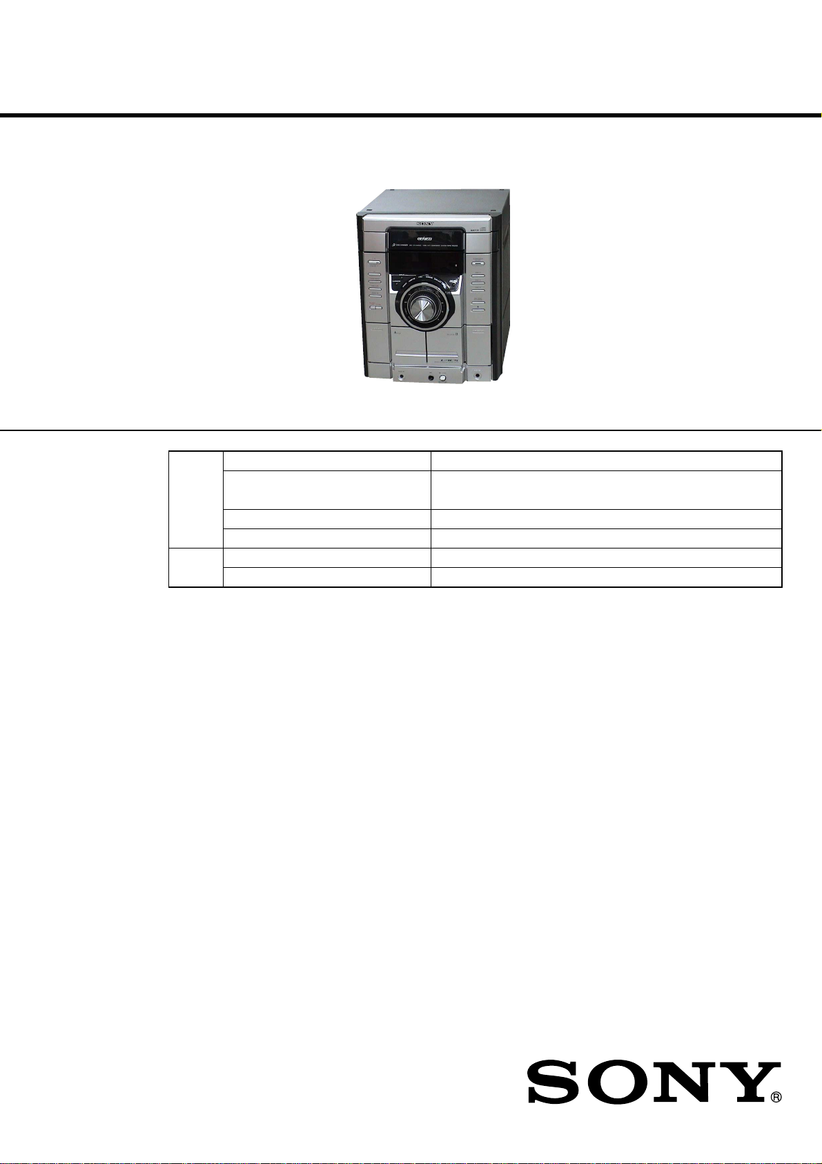
Photo: HCD-RG575
CDM74KFS-F1BD81C (Except Mexican model)/
CDM74KFS-F1BD84 (Mexican model)
US Model
Canadian Model
HCD-GX355/GX555
AEP Model
UK Model
Australian Model
HCD-RG270/RG475
E Model
HCD-RG270/RG475/RG575
Amplifier section
AUDIO POWER SPECIFICATIONS
(HCD-GX555/GX355 USA model only)
HCD-GX555
POWER OUTPUT AND TOTAL HARMONIC
DISTORTION:
With 6 ohm loads, both channels driven, from
120 – 10,000 Hz: rated 145 watts per channel
minimum RMS power, with no more than 10%
total harmonic distortion fro m 250 mill iwatts to
rated output.
HCD-GX355
POWER OUTPUT AND TOTAL HARMONIC
DISTORTION:
With 6 ohm loads, both channels driven, from
120 – 10,000 Hz: rated 150 watts per channel
minimum RMS power, with no more than 10%
total harmonic distortion fro m 250 mill iwatts to
rated output.
SPECIFICATIONS
North American model:
HCD-GX555
Front speaker
Continuous RMS power output (reference):
145 + 145 watts (6 ohms at
1 kHz, 10% THD)
Total harmonic distortion less than 0.07% (6 ohms at
1kHz, 80 W)
Sub woofer
Continuous RMS power output (reference):
170 watts (6 ohms at
80 Hz, 10% THD)
Total harmonic distortion less than 0.07% (6 ohms at
80 Hz, 90 W)
HCD-GX355
Continuous RMS power output (reference):
150 + 150 watts (6 ohms at
1 kHz, 10% THD)
Total harmonic distortion less than 0.07% (6 ohms at
1kHz, 80 W)
European and Russian models:
HCD-RG475
Front speaker
DIN power output (rated): 110 + 110 watts (6 ohms at
Continuous RMS power output (reference):
Music power output (reference):
Sub woofer
DIN power output (rated): 130 watts (6 ohms at
Continuous RMS power output (reference):
Music power output (reference):
HCD-RG270
DIN power output (rated): 80 + 80 watts (6 ohms at
Continuous RMS power output (reference):
Music power output (reference):
1kHz, DIN)
140 + 140 watts (6 ohms at
1kHz, 10% THD)
280 + 280 watts (6 ohms at
1kHz, 10% THD)
80 Hz, DIN)
160 watts (6 ohms at
80 Hz, 10% THD)
320 watts (6 ohms at
80 Hz, 10% THD)
1kHz, DIN)
100 + 100 watts (6 ohms at
1kHz, 10% THD)
200 + 200 watts (6 ohms at
1kHz,
10% THD)
– Continued on next page –
9-879-533-03
2005E05-1
© 2005.05
COMPACT DISC DECK RECEIVER
Sony Corporation
Personal Audio Group
Published by Sony Engineering Corporation

HCD-GX355/GX555/RG270/RG475/RG575
Other models :
HCD-RG575
The following measured at AC 120, 127, 220, 240 V
50/60 Hz
Front speaker
DIN power output (rated): 100 + 100 watts (6 ohms at
1kHz, DIN)
Continuous RMS power output (reference):
125 + 125 watts (6 ohms at
1kHz, 10% THD)
Sub woofer
DIN power output (rated): 120 watts (6 ohms at
80 Hz, DIN)
Continuous RMS power output (reference):
150 watts (6 ohms at
80 Hz, 10% THD)
HCD-RG475
Front speaker
The following measured at AC 120, 127, 220, 240 V
50/60 Hz
DIN power output (rated): 100 + 100 watts (6 ohms at
1kHz, DIN)
Continuous RMS power output (reference):
120 + 120 watts (6 ohms at
1kHz, 10% THD)
Sub woofer
DIN power output (rated): 120 watts (6 ohms at
80 Hz, DIN)
Continuous RMS power output (reference):
150 watts (6 ohms at
80 Hz, 10% THD)
HCD-RG270
The following measured at AC 120, 127, 220, 240 V
50/60 Hz
DIN power output (rated): 100 + 100 watts (6 ohms at
1kHz, DIN)
Continuous RMS power output (reference):
125 + 125 watts (6 ohms at
1kHz, 10% THD)
Inputs
AUDIO IN (stereo mini jack):
voltage 250 mV,
impedance 47 kilohms
MIC (phone jack) (Latin American model onl y) :
sensitivity 1 mV,
impedance 10 kilohms
Outputs
PHONES (stereo mini jack):
accepts headphones of
8ohms or more
VIDEO OUT (phono jack) (Mexican model only):
max. output level 1Vp-p,
unbalanced, Sync
negative, load impedance
75 ohms
SPEAKER: accepts impedance of 6 to
16 ohms
SUBWOOFER OUT (HCD-GX555/RG575/
RG475 only): accepts impedance of 6 to
16 ohms
CD player section
System Compact disc and digit al
Laser Diode Properties Emission duration:
*This output is the value measurement at a dist ance o f
200mm from the objective lens surf ace on the
Optical Pick-up Block with 7mm ape rture.
Frequency response 2 Hz – 20 kHz (±0.5 dB)
Signal-to-noise ratio More than 90 dB
Dynamic range More than 90
audio system
continuous
Laser Output*:
Less than 44.6µW
dB
Tape deck section
Recording system 4-track 2-channel, stereo
Frequency response 50 – 13,000 Hz (±3 dB),
using Sony TYPE I
cassettes
Tuner section
FM stereo, FM/AM superheterodyne tuner
FM tuner section
Tuning range
North American model: 87.5 – 108.0 MHz
Other models: 87.5 – 108.0 MHz
Antenna FM lead antenna
Antenna terminals 75 ohms unbalanced
Intermediate frequency 10.7 MHz
AM tuner section
Tuning range
Pan-American models: 530 – 1,710 kHz
European, Russian and Saudi Arabian mode ls:
Other models: 530 – 1,710 kHz
Antenna AM loop antenna
Intermediate frequency 450 kHz
(100 kHz step)
(50 kHz step)
(with the tuning interval
set at 10 kHz)
531 – 1,710 kHz
(with the tuning interval
set at 9 kHz)
531 – 1,602 kHz (with the
tuning interval set at
9kHz)
(with the tuning interval
set at 10 kHz)
531 – 1,602 kHz
(with the tuning interval
set at 9 kHz)
General
Power requirements
North American model: 120 V AC, 60 Hz
European and Russian models:
Australian model: 230 – 240 V AC, 50/60 Hz
Argentine model: 220 V AC, 50/60 Hz
Mexican model: 127 V AC, 60 Hz
Saudi Arabian model: 120 – 127, 220 or
Other models: 120 V, 220 V or
Power consumption
USA model:
HCD-GX555: 285 watts
HCD-GX355: 210 watts
Canadian model:
HCD-GX555: 380 VA
HCD-GX355: 290 VA
European and Russian models:
HCD-RG475: 300 watts
HCD-RG270: 190 watts
Other models:
HCD-RG575: 300 watts
HCD-RG475: 300 watts
HCD-RG270: 210 watts
Dimensions (w/h/d) (excl. speakers)
Mass (excl. speakers)
North American models:
HCD-GX555: Approx. 10.5 kg
HCD-GX355: Approx. 10.0 kg
Canadian model:
HCD-GX555: Approx. 10.5 kg
HCD-GX355: Approx. 10.0 kg
European and Russian models:
HCD-RG475: Approx. 10.5 kg
HCD-RG270: Approx. 8.7 kg
Other models:
HCD-RG575: Approx. 10.5 kg
HCD-RG475: Approx. 10.5 kg
HCD-RG270: Approx. 10.0 kg
Design and specifications are subject to change
without notice.
230 V AC, 50/60 Hz
230 – 240 V AC, 50/60 Hz
Adjustable with voltag e
selector
230 – 240 V AC, 50/60 Hz
Adjustable with voltag e
selector
0.25 watts (at the Power
Saving Mode)
0.25 watts (at the Power
Saving Mode)
Approx. 280 × 325
430 mm
2
HCD-GX355/GX555/RG270/RG475/RG575
r
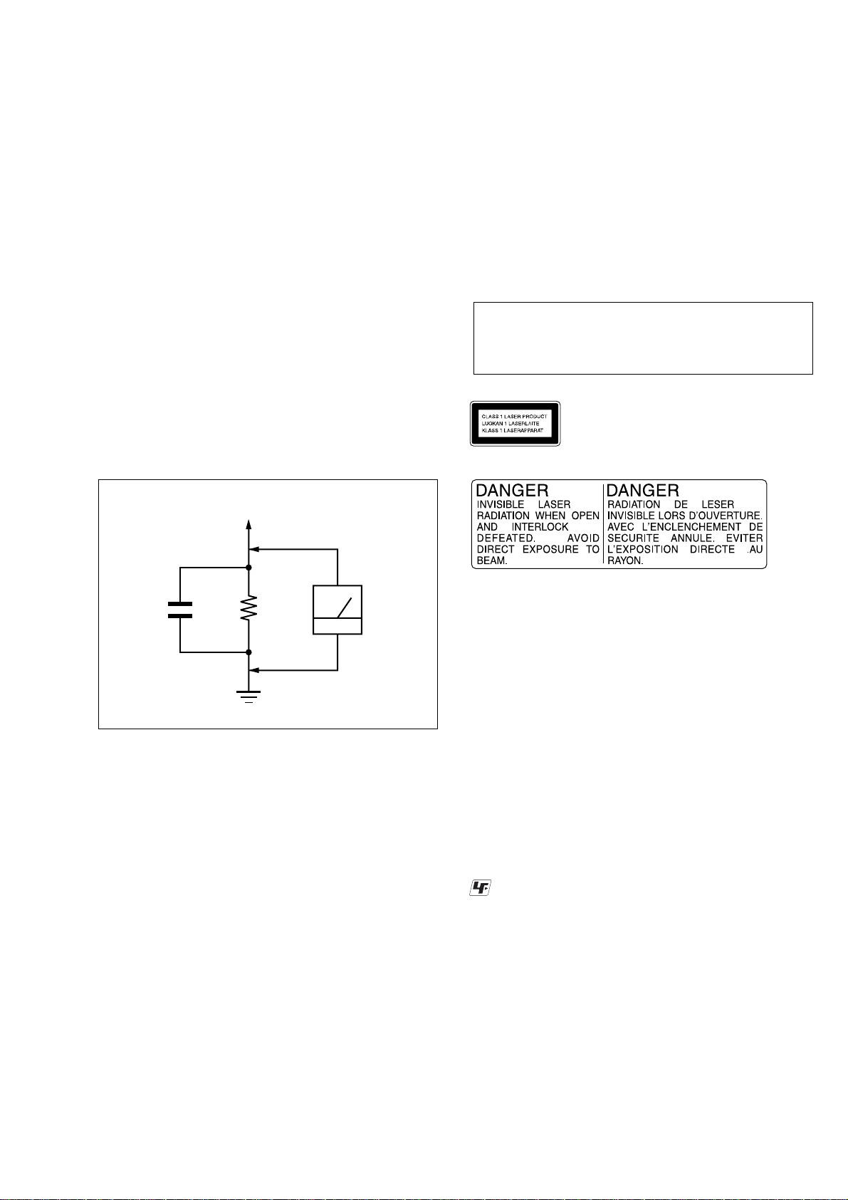
SAFETY CHECK-OUT
After correcting the original service problem, perform the following
safety check before releasing the set to the customer:
Check the antenna terminals, metal trim, “metallized” knobs, screws,
and all other exposed metal parts for AC leakage.
Check leakage as described below.
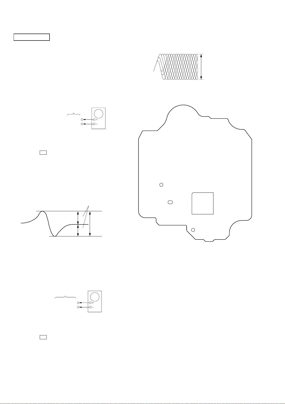
LEAKAGE TEST
The AC leakage from any exposed metal part to earth ground and
from all exposed metal parts to any exposed metal part having a
return to chassis, must not exceed 0.5 mA (500 microamperes.).
Leakage current can be measured by any one of three methods.
1. A commercial leakage tester, such as the Simpson 229 or RCA
WT -540A. Follow the manuf acturers’ instructions to use these
instruments.
2. A battery-operated A C milliammeter . The Data Precision 245
digital multimeter is suitable for this job.
3. Measuring the voltage drop across a resistor by means of a
VOM or battery-operated AC voltmeter . The “limit” indication
is 0.75 V, so analog meters must have an accurate low-voltage
scale. The Simpson 250 and Sanwa SH-63Trd are examples
of a passive VOM that is suitable. Nearly all battery operated
digital multimeters that have a 2 V A C range are suitable. (See
Fig. A)
To Exposed Metal
Parts on Set
Notes on chip component replacement
• Never reuse a disconnected chip component.
• Notice that the minus side of a tantalum capacitor may be
damaged by heat.
Flexible Circuit Board Repairing
• Keep the temperature of the soldering iron around 270 ˚C
during repairing.
• Do not touch the soldering iron on the same conductor of the
circuit board (within 3 times).
• Be careful not to apply force on the conductor when soldering
or unsoldering.
CAUTION
Use of controls or adjustments or performance of procedures
other than those specified herein may result in hazardous radiation
exposure.
This appliance is classified as
a CLASS 1 LASER product.
This marking is located on the
rear exterior.
AC
0.15 µF
1.5 k
Ω
Earth Ground
voltmete
(0.75 V)
Fig. A. Using an AC voltmeter to check AC leakage.
SAFETY-RELATED COMPONENT WARNING!!
COMPONENTS IDENTIFIED BY MARK 0 OR DOTTED LINE
WITH MARK 0 ON THE SCHEMATIC DIAGRAMS AND IN
THE PARTS LIST ARE CRITICAL TO SAFE OPERATION.
REPLACE THESE COMPONENTS WITH SONY PARTS WHOSE
PART NUMBERS APPEAR AS SHOWN IN THIS MANU AL OR
IN SUPPLEMENTS PUBLISHED BY SONY.
ATTENTION AU COMPOSANT AYANT RAPPORT
LES COMPOSANTS IDENTIFIÉS P AR UNE MARQ UE 0 SUR
LES DIAGRAMMES SCHÉMATIQUES ET LA LISTE DES
PIÈCES SONT CRITIQUES POUR LA SÉCURITÉ DE
FONCTIONNEMENT. NE REMPLACER CES COM- POSANTS
QUE PAR DES PIÈCES SONY DONT LES NUMÉROS SONT
DONNÉS DANS CE MANUEL OU DANS LES SUPPLÉMENTS
PUBLIÉS PAR SONY.
À LA SÉCURITÉ!
UNLEADED SOLDER
Boards requiring use of unleaded solder are printed with the leadfree mark (LF) indicating the solder contains no lead.
(Caution: Some printed circuit boards may not come printed with
the lead free mark due to their particular size)
: LEAD FREE MARK
Unleaded solder has the following characteristics.
• Unleaded solder melts at a temperature about 40 ˚C higher
than ordinary solder.
Ordinary soldering irons can be used but the iron tip has to be
applied to the solder joint for a slightly longer time.
Soldering irons using a temperature regulator should be set to
about 350 ˚C.
Caution: The printed pattern (copper foil) may peel away if
the heated tip is applied for too long, so be careful!
• Strong viscosity
Unleaded solder is more viscou-s (sticky, less prone to flow)
than ordinary solder so use caution not to let solder bridges
occur such as on IC pins, etc.
• Usable with ordinary solder
It is best to use only unleaded solder but unleaded solder may
also be added to ordinary solder.
3

HCD-GX355/GX555/RG270/RG475/RG575
Ver. 1.1
TABLE OF CONTENTS
1. SERVICING NOTES ............................................... 5
2. GENERAL ................................................................... 6
3. DISASSEMBLY
3-1. Disassembly Flow ........................................................... 8
3-2. Case (Top) ....................................................................... 9
3-3. Door (CD)........................................................................ 9
3-4. Front Panel Section ......................................................... 10
3-5 Mechanical Deck (CWM43FF13) ................................... 10
3-6. CD Mechanism Deck (CDM74KFS-F1BD81C (Except
MX model)/CDM74KFS-F1BD84 (MX model)) ........... 11
3-7. Back Panel Section .......................................................... 11
3-8. MAIN Board.................................................................... 12
3-9. BD Board/CD Board ....................................................... 12
3-10. DRIVER Board, SW Board............................................. 13
3-11. Optical Pick-up (KSM-215DCP) .................................... 13
3-12. SENSOR Board ............................................................... 14
3-13. MOTOR (TB) Board ....................................................... 14
3-14. MOTOR (LD) Board ....................................................... 15
4. TEST MODE.............................................................. 16
5. ELECTRICAL ADJUSTMENT............................ 20
6. DIAGRAMS
6-1. Block Diagram – CD SERVO Section – ........................ 21
6-2. Block Diagram – AUDIO/VIDEO Section – ................. 22
6-3. Block Diagram – AMP Section –................................... 23
6-4. Block Diagram
– PANEL, POWER SUPPLY Section – .......................... 24
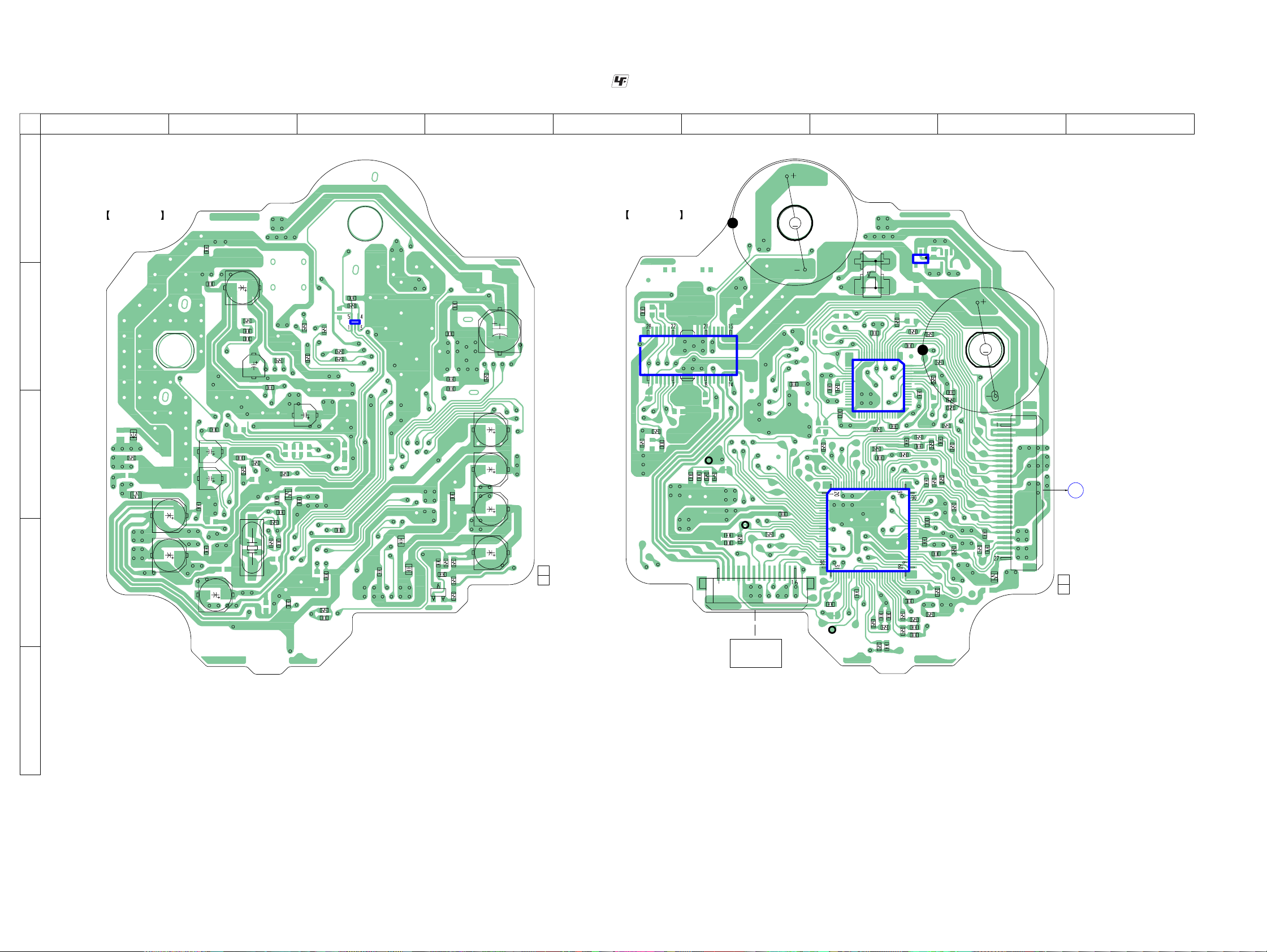
6-5. Printed Wiring Board
– CD Board – (Except MX model) ................................. 26
6-6. Schematic Diagram
– CD Board – (Except MX model) ................................. 27
6-7. Printed Wiring Board – BD Board – (MX model) ......... 28
6-8. Schematic Diagram – BD Board – (MX model) ............ 29
6-9. Printed Wiring Boards – CHANGER Section –............. 30
6-10. Schemtic Diagram – CHANGER Setion –..................... 31
6-11. Printed Wiring Board – MAIN Board – ......................... 32
6-12. Schematic Diagram – MAIN Board (1/3) – ................... 33
6-13. Schematic Diagram – MAIN Board (2/3) – ................... 34
6-14. Schematic Diagram – MAIN Board (3/3) – ................... 35
6-15. Printed Wiring Board – POWER Board – ...................... 36
6-16. Schematic Diagram –POWER Board –.......................... 37
6-17. Printed Wiring Board – SUB WOOFER Board –
(GX555/RG475/RG575 only) ......................................... 38
6-18. Schematic Diagram – SUB WOOFER Board –
(GX555/RG475/RG575 only) ......................................... 39
6-19. Printed Wiring Boards
– AUDIO, MIC, HEADPHONE Boards – ...................... 40
6-20. Schematic Diagram
– AUDIO, MIC, HEADPHONE Boards – ...................... 41
6-21. Printed Wiring Boards – CD-G Section –
(MX model only)............................................................. 42
6-22. Schematic Diagram – CD-G Section –
(MX model only)............................................................. 43
6-23. Printed Wiring Board – PANEL Section (1/2) ............... 44
6-24. Printed Wiring Board – PANEL Section (2/2) ............... 45
6-25. Schematic Diagram – PANEL Section (1/2) .................. 46
6-26. Schematic Diagram – PANEL Section (2/2) .................. 47
6-27. Printed Wiring Boards – TRANS Section – ................... 48
6-28. Schematic Diagram – TRANS Section – ....................... 49
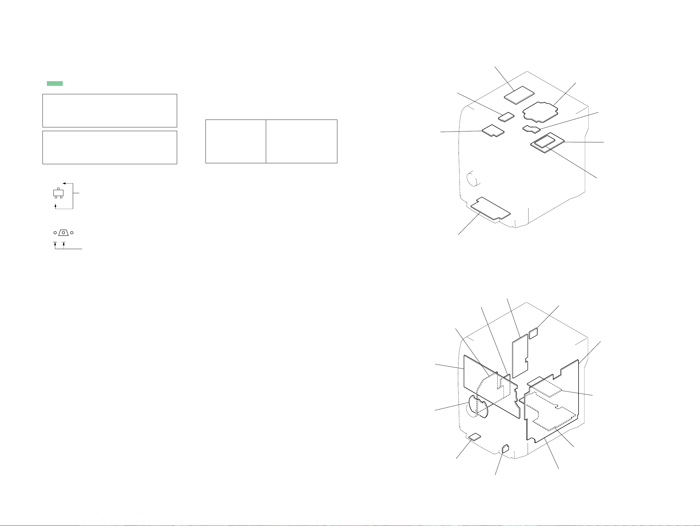
7. EXPLODED VIEWS
7-1. Overall Section ................................................................ 66
7-2. Back Panel Section .......................................................... 67
7-3. Front Panel Section ......................................................... 68
7-4. Key Section ..................................................................... 69
7-5. Chassis Section................................................................ 70
7-6. Transformer Section ........................................................ 71
7-7. CD Mechanism Deck Section-1
(CDM74KFS-F1BD81C) (Except MX model)/
(CDM74KFS-F1BD84) (MX model).............................. 72
7-8. CD Mechanism Deck Section-2
(CDM74KFS-F1BD81C) (Except MX model)/
(CDM74KFS-F1BD84) (MX model).............................. 73
8. ELECTRICAL PARTS LIST................................ 74
• Abbreviation
MX: Mexican model
4
HCD-GX355/GX555/RG270/RG475/RG575
l
SECTION 1
SERVICING NOTES
Ver. 1.1
NOTES ON HANDLING THE OPTICAL PICK-UP
BLOCK OR BASE UNIT
The laser diode in the optical pick-up block may suffer electrostatic
break-down because of the potential difference generated by the
charged electrostatic load, etc. on clothing and the human body.
During repair, pay attention to electrostatic break-down and also
use the procedure in the printed matter which is included in the
repair parts.
The flexible board is easily damaged and should be handled with
care.
NOTES ON LASER DIODE EMISSION CHECK
The laser beam on this model is concentrated so as to be focused on
the disc reflective surface by the objective lens in the optical pickup block. Therefore, when checking the laser diode emission,
observe from more than 30 cm away from the objective lens.
LASER DIODE AND FOCUS SEARCH OPERATION
CHECK
Carry out the “S curve check” in “CD section adjustment” and check
that the S curve waveforms is output three times.
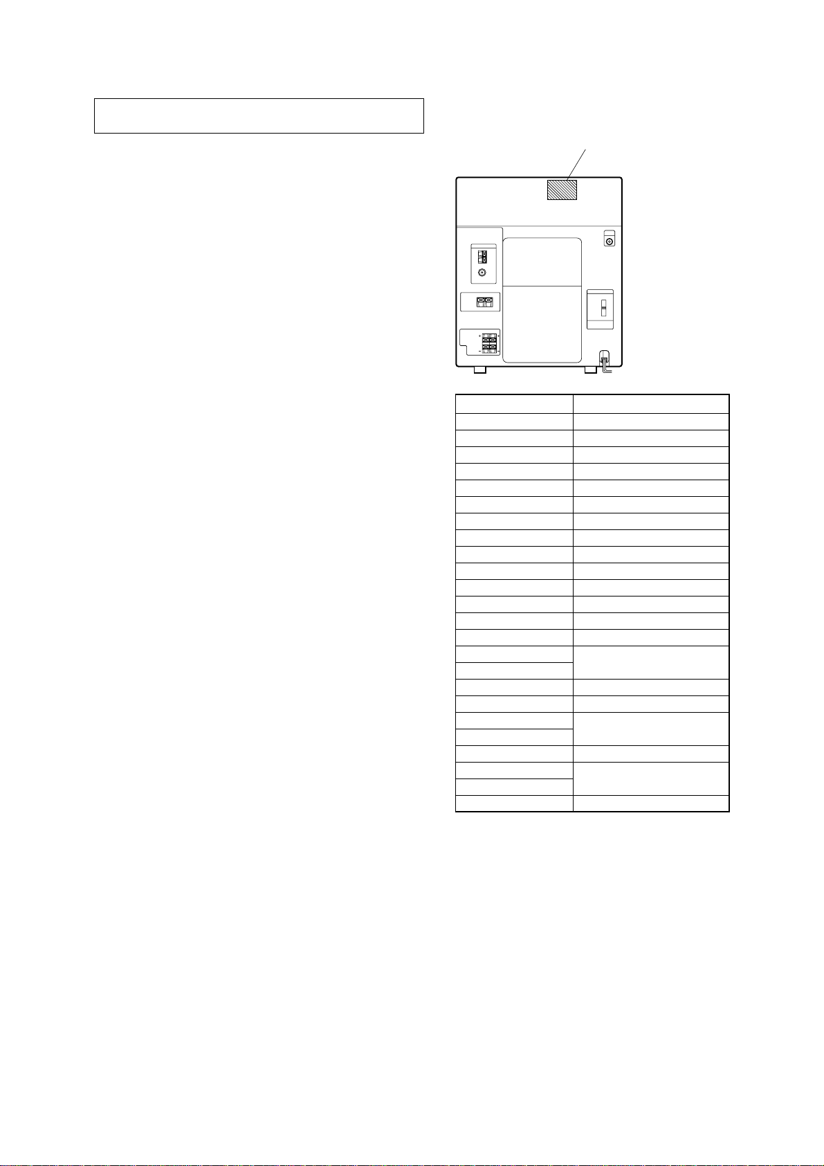
• MODEL IDENTIFICATION
– Back Panel –
Model number labe
Label indication Model
2-348-857-01 CA GX355: CND
2-560-970-01 U GX555: US
2-560-971-01 CA GX555: CND
2-560-972-01 CED RG475: AEP, UK, EE, RU
2-560-974-01 E3 RG475: E3
2-560-975-01 AU RG475: AUS
2-560-979-01 U GX355: US
2-560-980-01 CED RG270: AEP, UK, EE, RU
2-560-982-01 E3 RG270: E3
2-560-982-11 E2 RG270: E2
2-560-983-01 EA3 EA
2-560-984-01 SP2 RG475: SP
2-560-985-01 AU RG270: AUS
2-560-986-01 E51 RG270: E51
2-560-987-01 MX4
2-560-987-11 MX4
2-560-988-01 AR RG270: AR
2-560-995-01 SP2 RG575: SP
2-580-005-01 E2
2-580-005-11 E3
2-580-007-01 E51 RG575: E51
2-580-008-01 MX4
2-580-008-11 MX4
2-580-009-01 AR RG575: AR
RG270: MX
RG575: E2
RG575: MX
• Abbreviation
AR : Argentine model
AUS: Australian model
CND : Canadian model
E2 : 120V AC Area in E model
E3 : 240V AC Area in E model
E51 : Chilean and Peruvian models
EA : Saudi Arabia model
EE : East European model
MX : Mexican model
RU : Russian model
SP : Singapore model
5
HCD-GX355/GX555/RG270/RG475/RG575
123456789q
SECTION 2
GENERAL
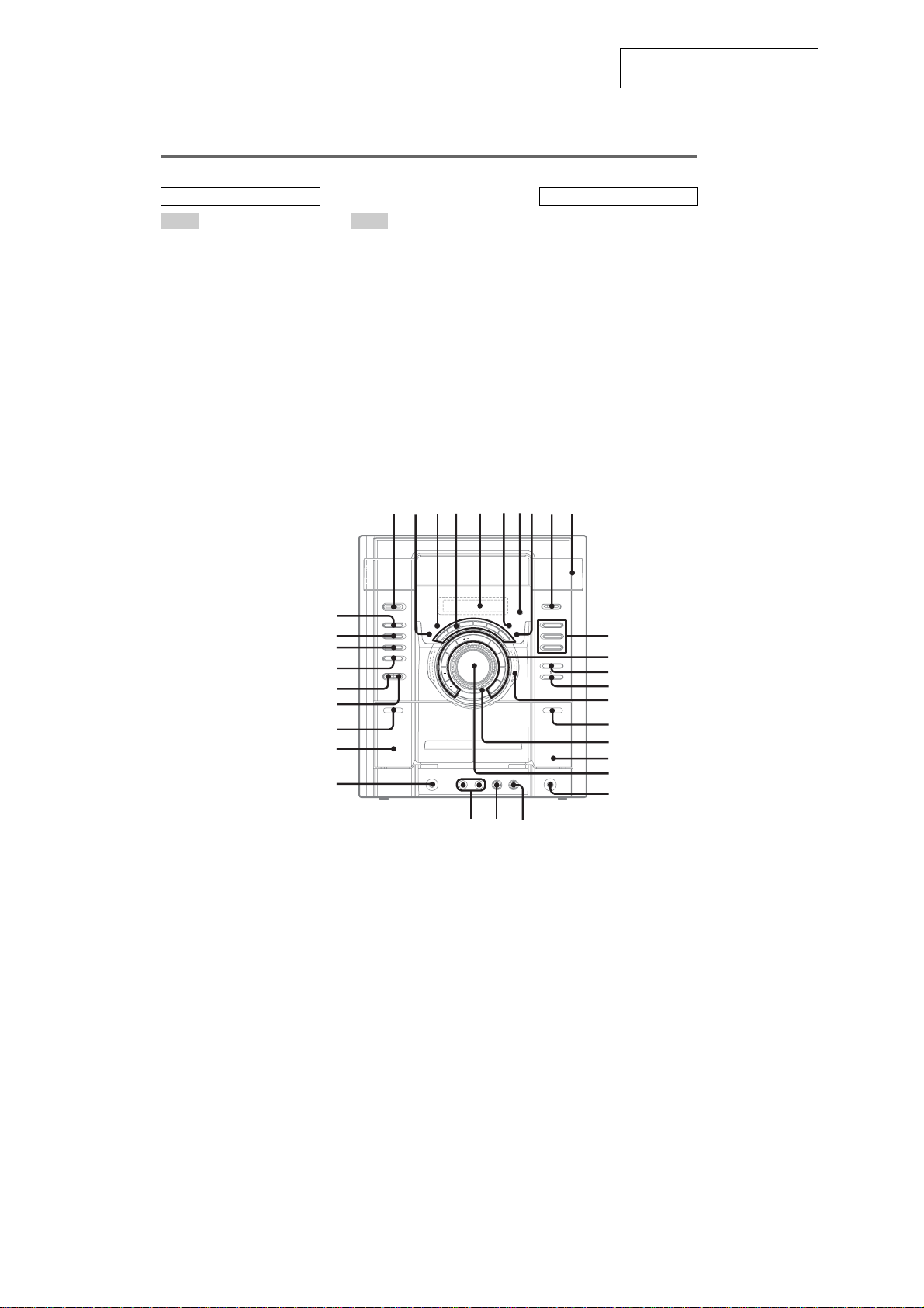
• Location of Controls
Main unit
ALPHABETICAL ORDER
A – O P – Z
ALBUM +/– qs
AUDIO IN wl
AUDIO IN jack wf
CD es
CD SYNC wj
Deck A wg
Deck B qk
DISC 1 – 3 qa
DISC SKIP/EX-CHANGE qd
Disc tray 0
DISPLAY 3
Display window 5
ECHO LEVEL
EFFECT ON/OFF 4
ENTER 4
EQ BAND qs
GROOVE 4
ILLUMINATION 2
MIC jack
MIC LEVEL
MULTIPLEX
Operation Dial
(– EQ +/l L/
– TUNING +) qj
2)
wd
2)
ws
1)
1)
6
wa
P FILE 4
PHONES jack w;
PLAY MODE 8
Power illuminator qg
PRESET EQ 4
REC PAUSE/START wl
Remote sensor 7
SUBWOOFER ON/OFF
SURROUND 4
TA P E A/B e;
TUNER/BAND ea
TUNING MODE 8
VOLUME control ql
es
ea
e;
wl
wk
wj
wh
wg
wf
This section is extracted from
instruction manual.
NS
3)
9
BUTTON DESCRIPTIO
?/1 (power) 1
X (pause) qs
x (stop) qs
M (fast forward) qs
N (play) qs
m (rewind) qs
Z (eject) qf
PUSH Z (deck B) (eject) qh
Z PUSH (deck A) (eject) wh
1)
Mexican model only
2)
Latin American model only
(Mexican model comes with
2microphone jacks)
3)
HCD-GX555/RG575/
RG475 only
;
L
l
j
A
H
S
s
B
qa
qs
qd
qf
qg
qh
qj
qk
ql
w;
6
wd
ws
wa
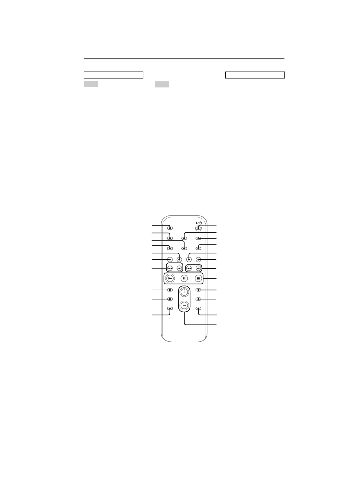
Remote control
HCD-GX355/GX555/RG270/RG475/RG575
ALPHABETICAL ORDER
A – E
ALBUM + qa
ALBUM – qd
CD qk
CLEAR qg
CLOCK/TIMER SELECT 2
CLOCK/TIMER SET 3
DISC SKIP q;
DISPLAY wa
ENTER 9
EQ qf
F – Z
FM MODE 4
FUNCTION 6
PLAY MODE w;
REPEAT 4
SLEEP ws
TAPE qj
TUNER BAND 5
TUNER MEMORY ql
TUNING MODE w;
VOLUME +/– qs
ws
wa
w;
ql
qk
qj
qh
BUTTON DESCRIPT
?/1 (power) 1
m/M (rewind/fast forward)
7
N (play) 8
X (pause) 8
x (stop) 8
+/– (tuning) qh
./> (go back/go forward)
qh
IONS
1
2
3
4
5
6
7
qg
qf
qd
8
9
q;
qa
qs
7
HCD-GX355/GX555/RG270/RG475/RG575
Ver. 1.1
SECTION 3
DISASSEMBLY
• This set can be disassembled in the order shown below.
3-1. DISASSEMBLY FLOW
SET
3-2. CASE (TOP)
(Page 9)
3-3. DOOR (CD)
(Page 9)
3-4. FRONT PANEL SECTION
(Page 10)
3-6. CD MECHANISM DECK
(CDM74KFS-F1BD81C (EXCEPT MX MODEL)/
CDM74KFS-F1BD84 (MX MODEL))
(Page 11)
3-7. BACK PANEL SECTION
(Page 11)
3-8. MAIN BOARD
(Page 12)
3-9. BD BOARD/
CD BOARD
(Page 12)
3-10. DRIVER BAORD,
3-5. MECHANICAL DECK
(CWM43FF13)
(Page 10)
3-11. OPTICAL PICK-UP
(KSM-215DCP)
(Page 13)
SW BOARD
(Page 13)
3-12. SENSOR BOARD
(Page 14)
3-13. MOTOR (TB) BOARD
(Page 14)
3-14. MOTOR (LD) BOARD
(Page 15)
8
Note: Follow the disassembly procedure in the numerical order given.
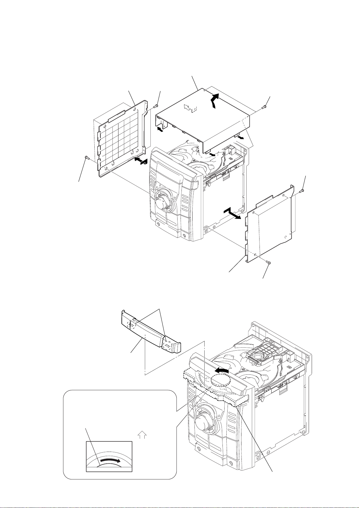
3-2. CASE (TOP)
0
5
6
case (side-R)
two screws (B3)
HCD-GX355/GX555/RG270/RG475/RG575
case (top)
7
two screws
8
4
three screws
(case 3 TP2)
3-3. DOOR (CD)
9
3
two claws
9
3
case (side-R)
8
1
three screws
(case 3 TP2)
2
two screws (B3)
4
door (CD)
–BOTTOM VIEW–
CD mechanism deck
1
Turn the pulley in the direction of the arrow.
Front panel side
2
Pull-out the disc tray.
9
HCD-GX355/GX555/RG270/RG475/RG575
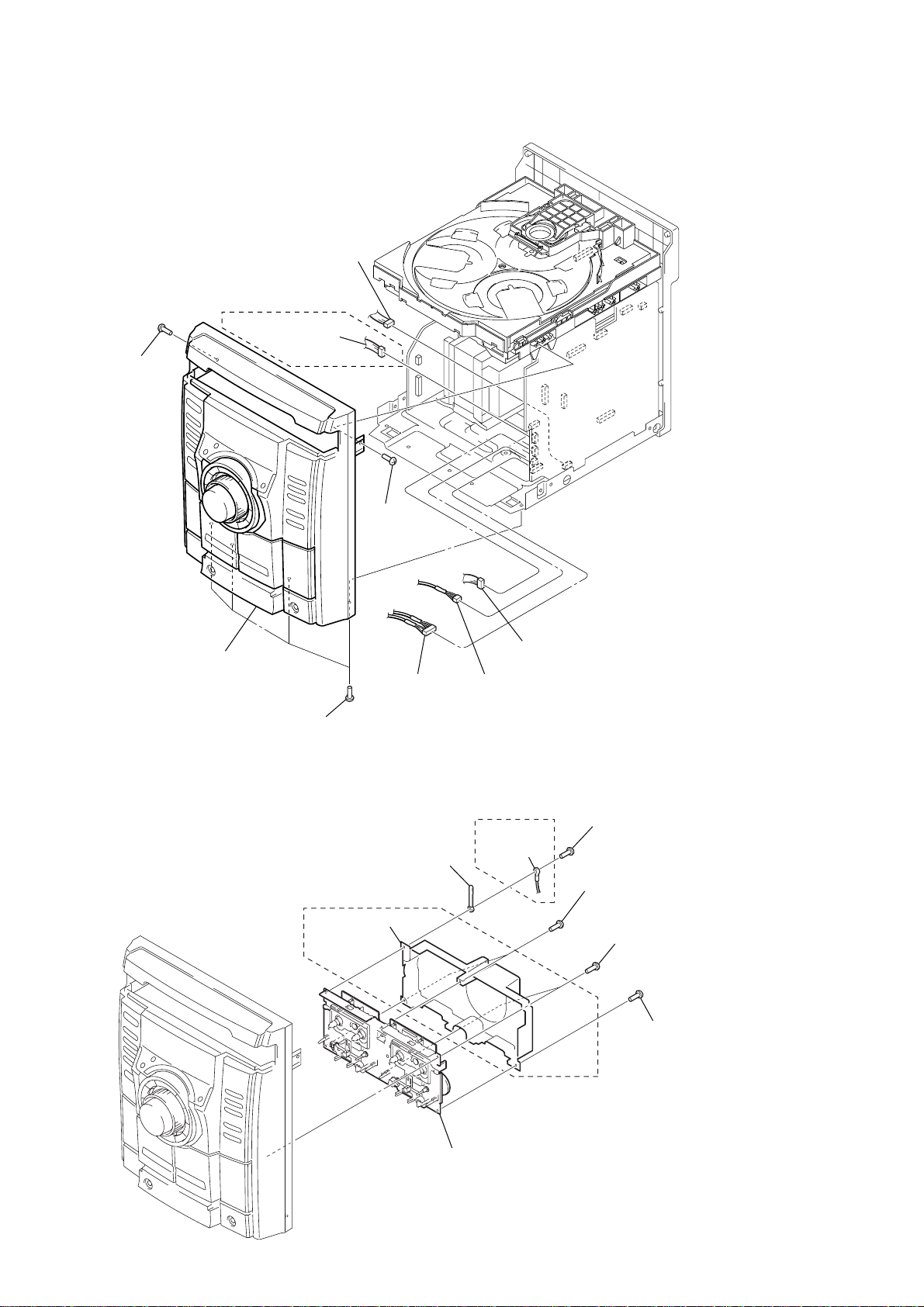
3-4. FRONT PANEL SECTION
•
Abbreviation
AR : Argentina model
E2 : 120V AC Area in E model
E51 : Chilean and Peruvian models
MX : Mexican model
1
connector
(CN061)
(E2, E51, AR, MX)
5
connector
(CN066)
8
screw (B3)
9
front panel section
6
four screws (B3)
3-5. MECHANICAL DECK (CWM43FF13)
•
Abbreviation
MX : Mexican model
(MX)
7
cover (TCM)
7
screw
(B3)
2
3
connector
(CN203)
coating clip
4
connector (CN065)
3
connector (CN201)
(except MX)
2
harness
1
screw
(2.6
5
two screws
(2.6
×
8)
×
8)
4
two screws
(2.6
×
8) (except MX)
(2.6 × 10) (MX)
10
8
mecanical deck
(CWM43FF13)
6
screw
(2.6 × 8)
HCD-GX355/GX555/RG270/RG475/RG575
3-6. CD MECHANISM DECK
(CDM74KFS-F1BD81C (EXCEPT MX MODEL)/CDM74KFS-F1BD84 (MX MODEL))
7
CD mechanism deck
(MX)
6
connector
(CN1004)
2
(CDM74KFS-F1BD81C (except MX)/CDM74KFS-F1BD84 (MX))
1
three screws (B3)
5
wire (flat type)
(13 core) (CN331)
Ver. 1.1
(MX)
3
wire (flat type) (13 core) (CN701)
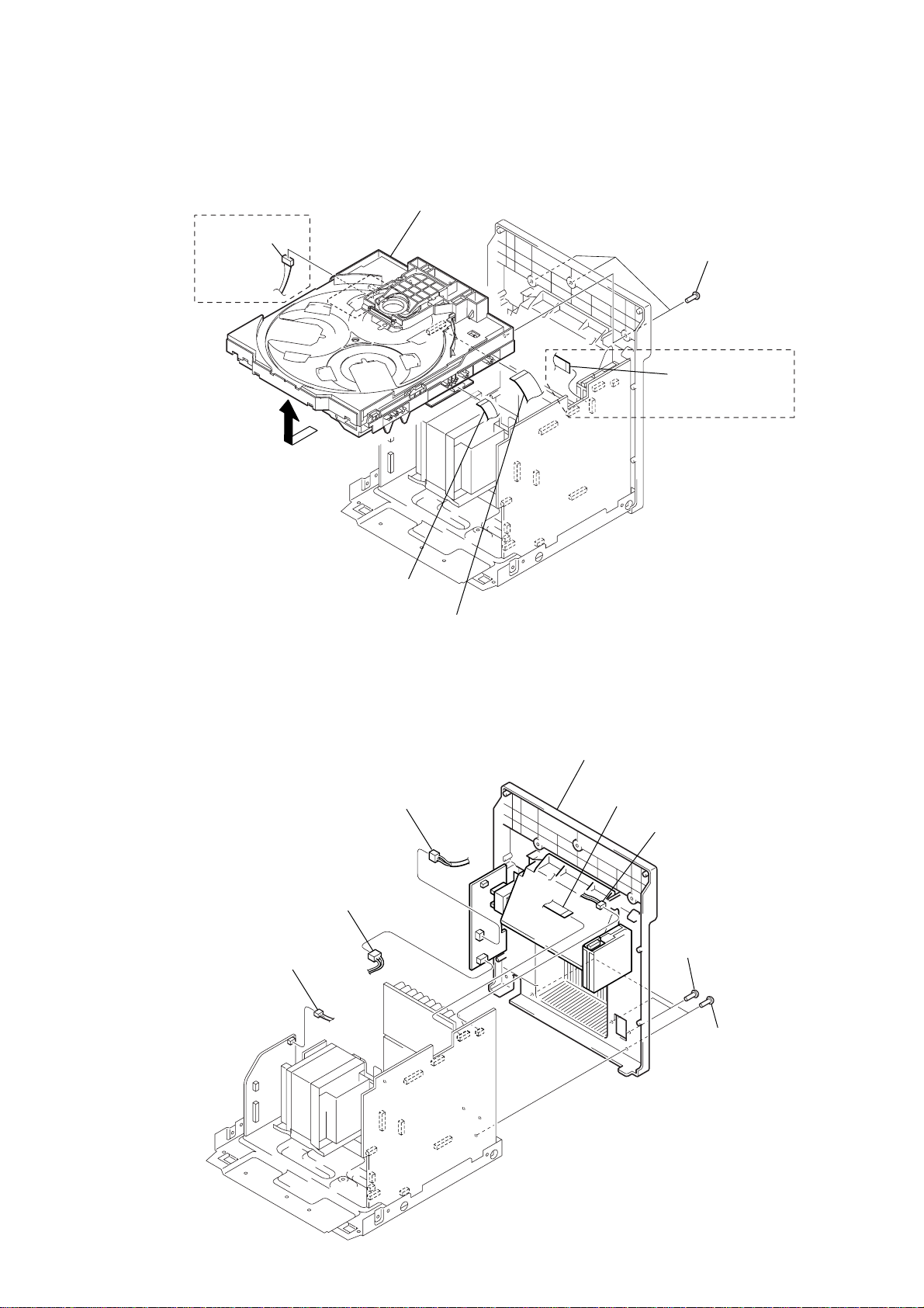
3-7. BACK PANEL SECTION
2
connector
(CN903)
1
connector
(CN906)
4
wire (flat type) (27 core) (CN201) (Except MX)
wire (flat type) (31 core) (CN201) (MX)
3
connector
(CN901)
•
Abbreviation
MX : Mexican model
8
back panel section
4
wire (flat type) (15 core)
(CN381)
5
connector
(CN041)
6
two screws (B3)
7
two screws (B3)
11
HCD-GX355/GX555/RG270/RG475/RG575
)
3-8. MAIN BOARD
5
MAIN board
4
connector
(CN441)
MAIN
board
1
connector
(CN907)
3-9. BD BOARD/CD BOARD
•
Abbreviation
MX : Mexican model
3
Remove soldering from the four points.
2
connector
(CN905)
3
two screws (B3)
2
screw
(+BVTP 2.6
4
BD
board (MX)/
CD
board (except MX)
1
× 8
)
wire (flat type) (16 core) (CN101
12
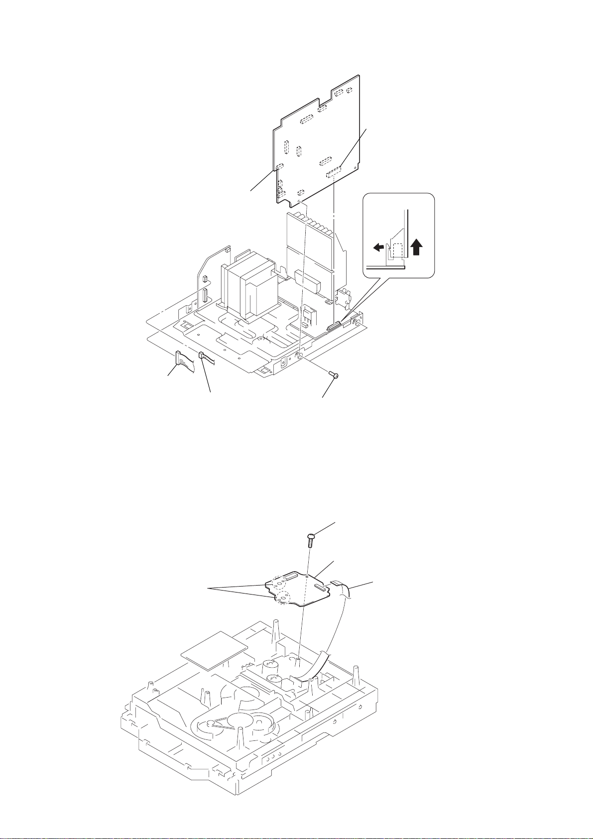
3-10. DRIVER BOARD, SW BOARD
1
two
screws
(+BTTP (M2.6))
4
DRIVER
board
2
wire (flat type) 5p (CN702)
HCD-GX355/GX555/RG270/RG475/RG575
Ver. 1.1
3
connector
4p (CN703)
5
screw
(+BTTP (M2.6))
6
SW board
3-11. OPTICAL PICK-UP (KSM-215DCP)
•
Abbreviation
MX : Mexican model
8
7
(insulator)
6
(+PTPWH M2.6)
2
h
older (213) ASSY
qf
optical pick-up
(KSM-215DCP)
two
insulators
two
coil springs
two floating
screw
9
1
floating
(+PTPWH M2.6)
5
two
insulators
4
two
coil springs
(insulator)
3
two floating
(+PTPWH M2.6)
qs
wire
(flat type)
(CN101)
qd
B
D board (MX)/
C
D board (except MX)
screw
screw
qa
Remove the four solderings of motor.
0
s
crew (+BVTP 2.6x 8)
13
HCD-GX355/GX555/RG270/RG475/RG575
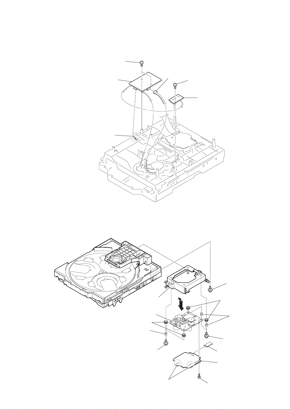
3-12. SENSOR BOARD
1
floating
screw
8
(+BTTP (M2.6))
screw
ear (geneva)
s
crew
2
t
ray
(+PTPWH M2.6)
6
floating
(+PTPWH M2.6)
7
g
0
SENSOR board
9
connector
(
CN731)
3
b
elt (table)
4
floating
(+PTPWH M2.6)
5
screw
p
ulley (table)
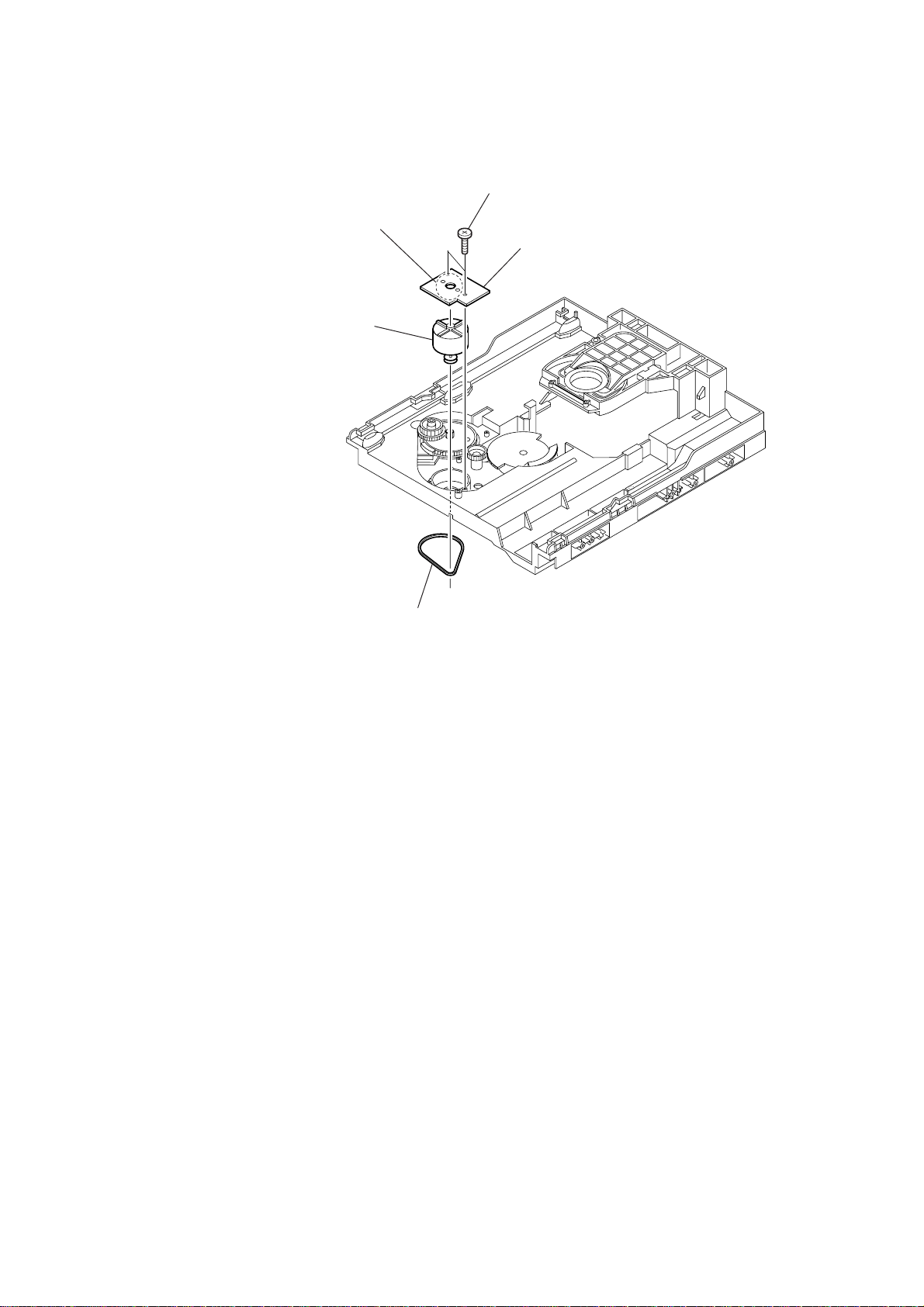
3-13. MOTOR (TB) BOARD
2
stopper
4
1
stopper
5
t
able motor assy (M741)
3
wire (flat type) 5 core (CN742)
7
MOTOR (TB) board
6
Remove the two solderings of motor.
14
5
two
screws
(+BTTP (M2.6))
3-14. MOTOR (LD) BOARD
4
Remove the two solderings of motor.
5
l
oading motor assy (M751)
HCD-GX355/GX555/RG270/RG475/RG575
2
two
screws
(+BTTP (M2.6))
3
MOTOR (LD) board
1
b
elt (loading)
15

HCD-GX355/GX555/RG270/RG475/RG575
[ --- EQ + ]
Ll
SECTION 4
TEST MODE
MC COLD RESET
The cold reset clears all data including preset data stored in the
RAM to initial conditions. Execute this mode when returning the
set to the customer.
Procedure:
1. Press three buttons of x , [ILLUMINATION] and [DISC 1]
simultane-ously.
2. The message “COLD RESET” is displayed on the fluorescent
indicator tube momentarily, then becomes standby states.
AM TUNING INTERVAL CHANGE-OVER
(Except AEP, UK, East European, Russian models)
A step of AM tuning interval can be changed over between 9 kHz
and 10 kHz.
Procedure:
1. Press the I/1 button to turn the power on.
2. Press the [TUNER/BAND] button to select “AM”.
3. Press the I/1 button to turn the power off.
4. Press two buttons of [PLAY MODE/TUNING MODE] and I/1
simultaneously.
5. The message “AM 9K STEP” or “ AM 10K STEP” is displayed
on the fluorescent indicator tube, and thus the channel step is
changed over.
CD SHIP (LOCK) MODE
This mode moves the optical pick-up to the position durable to
vibration. Use this mode when returning the set to the customer
after repair.
Procedure:
1. Press the I/1 button to turn the power on.
2. Press the [CD] button to select “CD”.
3. Press two buttons of [CD] and [POWER] simultaneously.
4. The message “LOCK” is displayed on the fluorescent indicator
tube, and the CD ship mode is set.
AMP TEST MODE
This mode is used to display the parameter of amplifier IC and
display the VACS status.
Procedure:
1. Press the I/1 button to turn the power on.
2. Press three buttons of x , [ILLUMINATION] and [PRESET EQ]
simultaneously.
3. When the AMP test mode is activated, the message “AMP
TEST IN” is displayed on the fluorescent indicator tube
momentarily, then amplif ier adjustment mode is displayed on
the fluorescent indicator tube.
4. Press the [DISPLAY] button to changed over between VACS
status display mode and the amplifier IC parameter display
mode.
5. In this mode, press the [GROOVE] button to changed over
DBFB on/off, and “DBFB ON” or “DBFB OFF” is displayed
on the fluorescent indicator tube.
6. In this mode, press the [SURROUND] button to changed over
surround on/off, and “SURROUND ON” or “SURROUND
OFF” is displayed on the fluorescent indicator tube.
7. In this mode, press the [EQ BAND] button to enter the equalizer
adjustment mode.
In the equalizer adjustment mode, press the [EQ BAND] button
to change over the adjustment band as LO W/MID/HIGH. And
turn the
each bands.
8. To release the amplifier IC parameter display mode or equalizer
adjustment mode, press the I/1 button to the power off.
knob to adjust the equalizer level of
CD SHIP (LOCK) MODE & COLD RESET
This mode is used to perform CD chip (lock) mode and cold reset
simultaneously.
Procedure:
1. Press the I/1 button to turn the power on.
2. Press the [CD] button to select “CD”.
3. Press three buttons of x , [CD] and [DISPLAY] simultaneously .
4. The message “COLD RESET” is displayed on the fluorescent
indicator tube momentarily, then becomes standby states.
CD TRAY LOCK MODE
This mode is used to unable to take sample disc out of tray in the
shop.
Procedure:
1. Press the I/1 button to turn the power on.
2. Press the [CD] button to select “CD”.
3. Load a disc and press two buttons of x and Z for 5 seconds.
4. The message “LOCKED” is displayed on the fluorescent
indicator tube and the CD tray is locked. (Even if pressing
the Z button, the message “LOCKED” is displayed on the
fluorescent indicator tube and the CD tray is locked)
5. To release this mode, press two buttons of x and Z for 5
seconds.
6. The message “UNLOCKED” is displayed on the fluorescent
indicator tube and the CD tray is unlocked.
16
HCD-GX355/GX555/RG270/RG475/RG575
AGING MODE
This mode can be used for operation check of CD section and tape
deck section.
CD section and tape deck section work in parallel.
If an error occurred:
The aging operation stops only an error occurred sections and display
then status.
If no error occurs:
The aging operation continues repeatedly.
Procedure:
1. Press the I/1 button to turn the power on.
2. Press the [CD] button to select “CD”.
3. Load three discs and insert two tape to the deck A and B.
4. Press three buttons of x , [ILLUMINATION] and [DISC SKIP/EX-
CHANGE] simultaneously.
5. Aging operations of CD and tape are started at the same time.
6. To release this mode, press the I/1 button to turn the power
off or press the function buttons to change the function.
1. Display at the Aging Mode
Display operating state of CD section and tape deck section
alternately.
If an error occurred, stop display which that section.
2. CD Section
The sequence during the aging mode is following as below.
Display at the aging mode is the same as the normal operation.
Aging mode sequence (CD section) :
3. Tape Deck Section
The sequence during the aging mode is following as below.
If an error occurred, stop display that step.
Aging mode sequence (tape deck section) :
Rewind the tape A and B
“TAPE AAG-1 or TAPE BAG-2”
Shut off
FWD play the tape A
“TAPE AAG-3”
2 minutes
Rewind the tape A
“TAPE AAG-6”
Shut off
FWD play the tape B
“TAPE BAG-3”
2 minutes
Rewind the tape B
“TAPE BAG-6”
Shut off
Start (from disc 1)
Disc chucking
TOC read
Play first track for 2 seconds
Play last track for 2 seconds
EX-change open/close
Open the disc tray
Disc skip
Close the tray
Change the next disc.
Note: “TAPE *AG-*” is display of each step.
PANEL TEST MODE
This mode is used to check the fluorescent indicator tube, LEDs
and buttons.
Procedure:
1. Press the I/1 button to turn the power on.
2. Press three buttons of x , [ILLUMINATION] and [GROOVE]
simultaneously.
3. Fluorescent indicator tube and LEDs are all turned on.
4. Press two buttons of [ALBUM ---] and [ENTER] simultaneously,
mode is changed over.
5. In the key check mode, press each key , the defined key number
of every each key list is displayed on the fluorescent indicator
tube.
6. In the key count check mode, “KEYCNT 0” is displayed on
the fluorescent indicator tube. Each time a key is pressed, “K”
value increases. Howe ver , once a key is pressed, it is no longer
taken into account.
7. In the headphone input check mode, connect the headphone,
the message “H_P ON” is displayed on the fluorescent
indicator tube, and disconnect the headphone, the message
“H_P OFF” is displayed on the fluorescent indicator tube.
8. In the volume check mode, “VOLUME FLAT” is displayed
on the fluorescent indicator tube. Turn the [MASTER
VOLUME] knob clockwise, the message “VOLUME UP”
is displayed on the fluorescent indicator tube momentarily
and turn the [MASTER VOLUME] knob counterclockwise,
the message “VOLUME DOWN” is displayed on the
fluorescent indicator tube momentarily.
17
HCD-GX355/GX555/RG270/RG475/RG575
MC TEST MODE
This mode is used to check operations of microprocessor.
Procedure:
1. Press the I/1 button to turn the power on.
2. Press three buttons of x , [ILLUMINATION] and [DISC 3]
simultane-ously.
3. When the MC test mode is activated, VACS level is displayed
on the fluorescent indicator tube momentarily.
4. Turn the
[ --- EQ + ]
Ll
knob clockwise, the message
“ALL EQ MAX” is displayed on the fluorescent indicator
tube momentarily and turn the
[ --- EQ + ]
Ll
knob
counter-clockwise, the message “ALL EQ MIN” is
displayed on the fluorescent indicator tube momentarily.
5. Press the [PRESET EQ] button, the message “ ALL EQ FLAT”
is displayed on the fluorescent indicator tube momentarily.
6. Turn the [MASTER VOLUME] knob clockwise, the message
“VOLUME MAX” is displayed on the fluorescent indicator
tube momentarily and turn the [MASTER VOLUME] knob
counterclockwise, the message “VOLUME MIN” is displayed
on the fluorescent indicator tube momentarily.
7. Press the [GROOVE] button to changed over VACS on/off.
8. When the [CD SYNC] key is pressed with the test tape (AMS-
100, AMS-110A) in the deck, number of space between tunes
is counted, then if AMS-110A is set, “OK” is displayed on the
fluorescent indicator tube and if AMS-100 is set, “NG” is
displayed on the fluorescent indicator tube.
9. Press the I/1 button to release from this mode, then cold reset
is performed.
VERSION DISPLAY MODE
This mode is used to check the model, destination and software
version.
Procedure:
1. Press the I/1 button to turn the power on.
2. Press three buttons of x , [ILLUMINATION] and [DISC 2]
simultane-ously.
3. When this mode is activated, model and destination is displayed
on the fluorescent indicator tube.
4. Press the [DISPLAY] button to changed ov er between software
version and year, month, day of the software creation display
mode and model and destination display mode.
5. To release this mode, press three buttons of x , [ILLUMI
NATION] and [DISC 2] simultaneously.
CD ERROR CODE DISPLAY MODE
This mode can be used for error code display of CD section.
Procedure:
1. Press the I/1 button to turn the power on.
2. Press the [CD] key to select “CD”.
3. Press three buttons of x , [CD] and [DISC 1] simultaneously.
4. When this mode is activated, mechanism deck error code is
displayed on the fluorescent indicator tube.
5. Press the [GROOVE] button to changed over between optical
pick-up error code display mode and mechanism deck error
code mode.
6. Turn the
[ --- EQ + ]
history.
7. To release this mode, press the I/1 button to turn the power
off.
Ll
knob to change o ver display of error
1. Mechanism Deck Error Code Mode
When this mode is entered, mechanism deck error code is displayed
with the 10-character format on the fluorescent indicator tube.
The first digit from the left indicates:
The first digit from the left indicates which mode the error history
is. In the mechanism deck error code mode, “M” is displayed on
the fluorescent indicator tube.
The second digit from the left indicates:
(Error history number display)
The second digit from the left indicates which order the error history
is. “1” indicates the latest error history, and each time the number
increases by one, the error history goes back to one-previous error.
The third and 4th digit from the left indicates:
(Error status display)
The third and 4th digit from the left indicates which error status is
indicated.
Display Status
00 No error
08 Table operation time-out (Table does not mov e to the target
position within the specified time)
16 In the chucking down operation, the operation was retried
by the maximum number of times but the operation could
not be completed
17 In the chucking up and down operation, the reverse
recovery processing was attempted but it could not be
recovered
18 In the chucking up operation, the operation was retried by
the maximum number of times but the operation could not
be completed
20 Loading operation time-out (Table does not move to the
target position within the specified time)
22 As the chuck was in the ex-open status at the initialization,
the closing was attempted but could not be completed
The 5th and 6th digit from the left indicates:
(Present status display)
The 5th and 6th digit from the left indicates which operating status
when an error occurred is indicated.
Display Status
01 Open completion status
02 From open status, the movement to c hucking down position
is under way
03 From chucking down position, the open operation is under
way
04 Chucking down completion status
10 The chucking down operation is under way
11 The chucking up operation is under way
12 Close completion status
13 From close status, the ex-open operation is under way
14 From ex-open status, the close operation is under way
18 Ex-pen completion status
18
HCD-GX355/GX555/RG270/RG475/RG575
The 7th and 8th digit from the left indicates:
(Motor status display)
The 7th and 8th digit from the left indicates which motor output
status when an error occurred is indicated.
Display Status
× 0 No table motor output
× 1Table motor forward output
× 2Table motor backward output
× 3Table motor break output
0 × No loading motor output
1 × Loading motor forward output
2 × Loading motor backward output
3 × Loading motor break output
The 9th and 10 th digit from the left indicates:
(Tray status display)
The 9th and 10th digit from the left indicates which target processing
when an error occurred is indicated.
Display Status
01 Open operation
12 Close operation
18 Ex-open operation
2. Optical Pick-up Error Code Mode
When this mode is entered, optical pick-up error code is displayed
with the 8-character format on the fluorescent indicator tube.
The first digit from the left indicates:
The first digit from the left indicates which mode the error history
is. In the optical pick-up error code mode, “D” is displayed on the
fluorescent indicator tube.
The second digit from the left indicates:
(Error history No. display)
The second digit from the left indicates which order the error history
is. “1” indicates the latest error history, and each time the number
increases by one, the error history goes back to one-previous error .
The 5th and 6th digit from the left indicates:
(Error step display)
The 5th and 6th digit from the left indicates which processing when
a trouble occurred
Display Contents
01 Power OFF in progress
02 Initialize in progress
03 Oscillation stopping
04 From oscillation stop, oscillation starting
05 Stopping
06 Stop operation is under way
07 Start operation in progress
08 TOC read in progress
09 Search operation is under way
0A Playback operation is under way
0B Pause operation is under way
0C Playback manual search operation is under way
0D Pause manual search operation is under way
0E —
The 7th and 8th digit from the left indicates:
The 7th and 8th digit from the left indicates which operation in
progress when a trouble occurred. (Step of each processing of the
5th and 6th digits is indicated)
5 REPEAT LIMIT CANCEL MODE
Number of repeat for CD playback is 5 times when the repeat mode
is “REPEAT”. This mode is used to enables CD to repeat playback
for limitless times.
Procedure:
1. Press the I/1 button to turn the power on.
2. Press the [CD] button to select “CD”.
3. Press three buttons of x , [CD] and [PLAY MODE/TUNING
MODE] simultaneously.
4. The message “LIMIT OFF” is displayed on the fluorescent
indicator tube momentarily, CD repeat 5 limit is cancelled.
The third and 4th digit from the left indicates:
(Error status display)
The third and 4th digit from the left indicates which error status is
indicated.
Display Status
01 Not focused (TOC read without a disc)
02 GFS NG (TOC read with a disc chucked)
03 Start operation time-over
04 Defocused continuously (Defocused during TOC reading)
05 Q code not entered for specified time
06 Tracking not turned ON
07 Blank disc (Blank disc TOC read)
19
HCD-GX355/GX555/RG270/RG475/RG575
e
p
p
SECTION 5
ELECTRICAL ADJUSTMENTS
CD SECTION
Note:
1. CD Block is basically designed to operate without adjustment.
Therefore, check each item in order given.
2. Use YEDS-18 (3-702-101-01) unless otherwise indicated.
3. Use an oscilloscope with more than 10MΩ impedance.
4. Clean the object lens by an applicator with neutral detergent when the
signal level is low than specified value with the following checks.
• Abbreviation
MX: Mexican model
S-CURVE CHECK
CD board (except MX)
BD board (MX)
TP(FE)
TP(VC)
Procedure:
1. Connect an oscilloscope to TP (FE) and TP (VC) on the CD
board (except MX) or BD board (MX).
2. Press the I/1 button to turn the power on.
3. Load the disc (YEDS-18) and actuate the focus search. (In
consequence of open and close the disc tray, actuate the focus
search)
4. Confirm that the oscilloscope waveform (S-curve) is
symmetrical between A and B. And conf irm peak to peak level
within 3 ± 0.5 Vp-p.
oscilloscop
RF signal waveform
VOLT/DIV : 200mV
TIME/DIV : 500ns
level : 1.3
±
0.3 Vp-
– CD BOARD (Conductor Side) (except MX) –
– BD BOARD (Conductor Side) (MX) –
TP
(VC)
S-curve waveform
symmetry
A
within 3
±
0.5 Vp-
B
Note: • Try to measure several times to make sure than the ratio of A : B
or B : A is more than 10 : 7.
• Take sweep time as long as possible and light up the brightness
to obtain best waveform.
Connecting Location: CD board (except MX)
BD board (MX)
RFAC LEVEL CHECK
CD board (except MX)
BD board (MX)
TP(RFACO)
TP(VC)
Procedure:
1. Connect an oscilloscope to TP (RFACO) and TP (VC) on the
CD board (except MX) or BD board (MX).
2. Press the I/1 button to turn the power on.
3. Load the disc (YEDS-18) and playback.
4. Confirm that oscilloscope waveform is clear and check if RF A C
signal level is correct or not.
Note: Clear RFAC signal waveform means that the shape “ ◊ ” can be clearly
distinguished at the center of the waveform.
oscilloscope
TP
(FE)
IC101
TP
(RFACO)
Connecting Location: CD board (except MX)
BD board (MX)
20
SECTION 6
DIAGRAMS
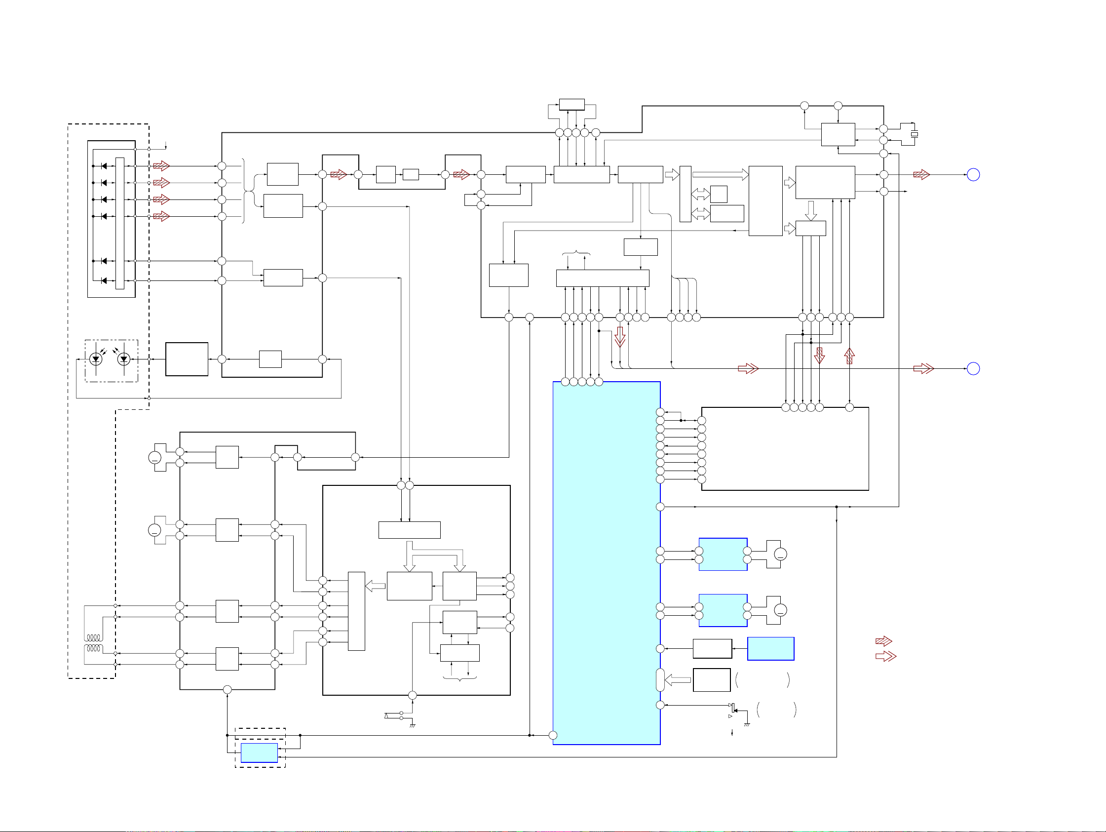
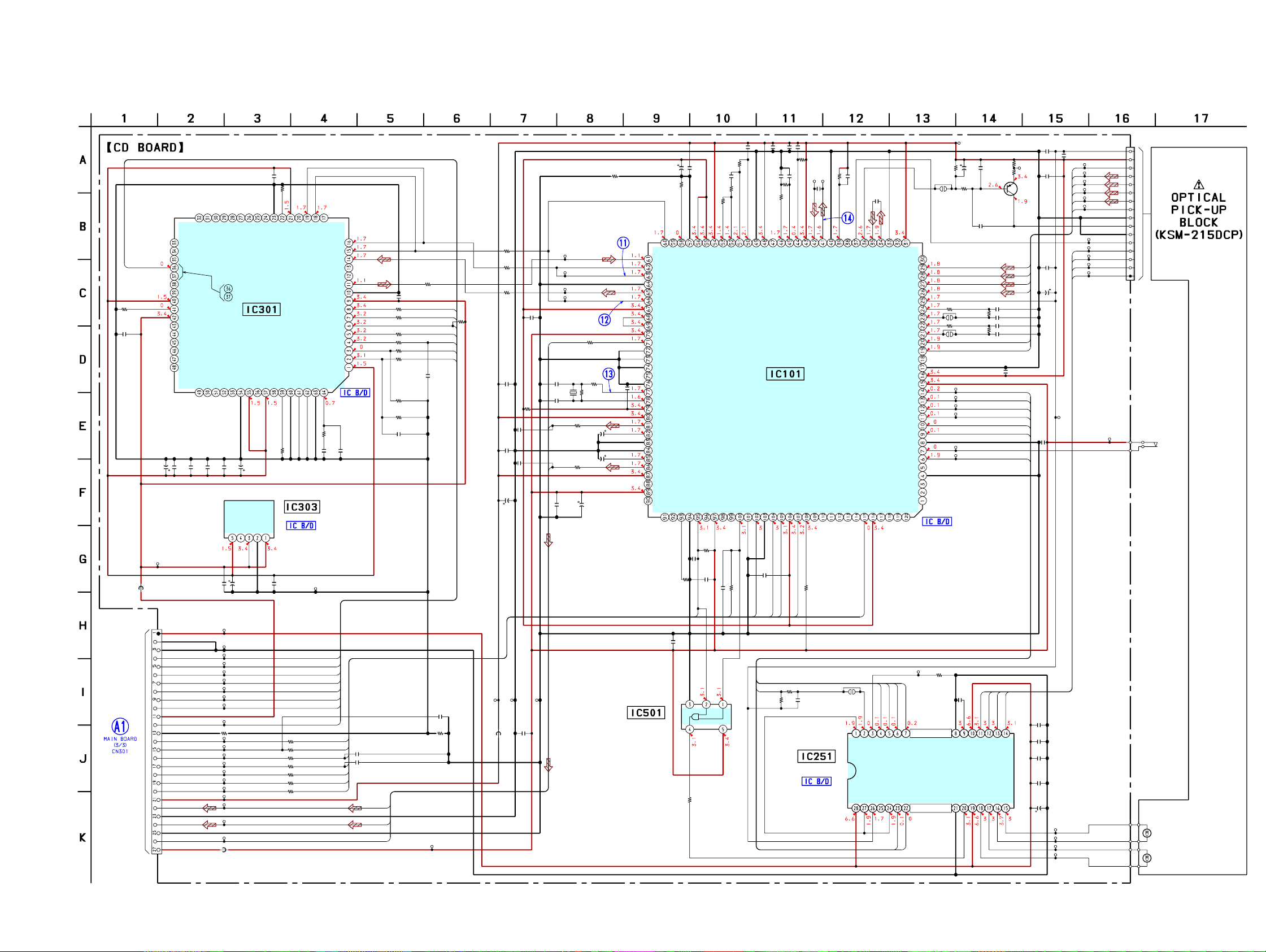
6-1. BLOCK DIAGRAM – CD SERVO Section –
HCD-GX355/GX555/RG270/RG475/RG575
Ver. 1.1
DETECTOR
A
B
C
D
F
E
OPTICAL PICK-UP
BLOCK
(KSM-215DCP)
LASER DIODE
PD
I-V AMP
LD
CD +3V
AUTOMATIC
POWER
CONTROL
Q10
CD DSP
IC101 (1/2) (EXCEPT MX)
IC101 (1/2) (MX)
A
26
B
27
C
28
D
29
F
20
E
19
LD
36
SUMMING
AMP
FOCUS
ERROR
TRACKING
ERROR AMP
APC LD
AMP
RF
AMP
AC_
SUM
FEO
TEO
EQ_
IN
34
24
22
PD
37
RFAC
35
VCA
RFACO
EQ
41
42
45
46
RFACI
ASYI
ASYO
DIGITAL
CLV
PROCESSOR
MDP
6
ASYMMETRY
CORRECTOR
XRST
100
FILTER
51 53
FILI
PCO
FILO
CLTV
DIGITAL PLL
TO SERVO AUTO
SEQUENCER
CPU INTERFACE
DATA
CLOCK
XLAT
31
33 45
32 19
1125052
XPCK
SCOR
SENS
SBSO
98 99115107102 105 104 110 111
SCOR
SBSO
EFM
DEMODULATOR
SUBCODE
PROCESSOR
SQCK
SQSO
EXCK
96 97
EXCK
WFCK
WFCK
XUGF
INTERNAL BUS
GFS
EMPH
68
113
32K
RAM
ERROR
CORRECTOR
D/A
DIGITAL
INTERFACE
117 93
C4M
GENERATOR
D/A
CONVERTER
SELECTOR
LRCK
BCK
PCMD
63 66 65
XTSL
CLOCK
LRCKI
BCKI
62 60 61
PCMDI
XTAO
XTAI
XTACN
AOUT1
AOUT2
77
78
95
81
86
R-CH
X171
16.9344MHz
SCOR, SBSO,
EXCK, WFCK
CD-L
A
B
(Page 22)
(Page 22)
2-AXIS
DEVICE
(TRACKING)
(FOCUS)
M101
(SPINDLE)
M102
(SLED)
O-XLT
I-SCOR
47
O-CD-CLK
O-CD-DATA
SYSTEM CONTROLLER
O-XRST
I-CD-SENS
IC901 (1/4)
MOTOR/COIL DRIVE
IC251 (EXCEPT MX)
IC251 (MX)
CH4OUTF
16
M
M
15
17
18
14
13
12
11
CH4OUTF
CH3OUTF
CH3OUTR
CH1OUTF
CH1OUTR
CH2OUTF
CH2OUTR
MOTOR
DRIVE
MOTOR
DRIVE
DRIVE
DRIVE
MUTE
COIL
COIL
20
CH4IN
CH3FIN
CH3RIN
CH1FIN
CH1RIN
CH2FIN
CH2RIN
(MX)
SWITCHING
IC501
(EXCEPT MX)
OPIN+
24
23
21
4
5
5
7
OPOUT
27
9
10
11
12
13
14
2
CD DSP
IC101 (2/2) (EXCEPT MX)
IC101 (2/2) (MX)
SFDR
SRDR
TFDR
TRDR
FFDR
FRDR
PWM GENERATOR
FOCUS/TRACKING/SLED
S101
(LIMIT)
21 23
FEI
TEI
A/D
CONVERTER
FOCUS/
TRACKING/SLED
SERVO DSP
SSTP
7
MIRR,
DFCT, FOK
DETECTOR
SERVO
INTERFACE
SERVO AUTO
SEQUENCER
TO CPU INTERFACE
FOK
MIRR
DFCT
COUT
SCLK
3
1
2
119
108
I-MP3-DI
O-MP3-DATA
O-MP3-CLK
O-MP3-CS
I-MP3-ACK
I-MP3-REQ
O-MP3-LP
O-MP3-RESET
O-MP3-STB
O-XTCN
I-E-1 – I-E-3
29
30
28
39
40
43
44
38
42
34
49O-LM-F
48O-LM-R
51O-TM-F
50O-TM-R
73I-CD-NUMBER-SENS
56I-OPEN-SW
52 – 54
MIDIO
6
MICK
7
MICS
4
MIACK
8
PO11/BUCK/AD14
36
MILP
5
RESET
2
3
STANDBY
LOADING MOTOR DRIVE
IC701
7 FIN
9 RIN
TABLE MOTOR DRIVE
IC712
7 FIN
9 RIN
LEVEL SHIFT
Q731
ROTARY
ENCODER
S711
ADDRESS DETECT
OPEN
CLOSE
4OUT1
2OUT2
4OUT1
2OUT2
TABLE ADDRESS
SENSOR
IC731
DISC TRAY
OPEN/CLOSE
DETECT
M
M
S751
16
19
18 14
SBSY/BCKIB
SFSY/LRCKIB
M751
(LOADING)
M741
(TABLE)
15
SDI0
BCKIA
LRCKIA
MP3 DECODER
IC301 (EXCEPT MX)
IC301 (MX)
11
SDO0
• Abbreviation
MX : Mexican model
• R-ch is omitted due to same as L-ch.
• SIGNAL PATH
: CD PLAY
: VIDEO
HCD-GX355/GX555/RG270/RG475/RG575
2121
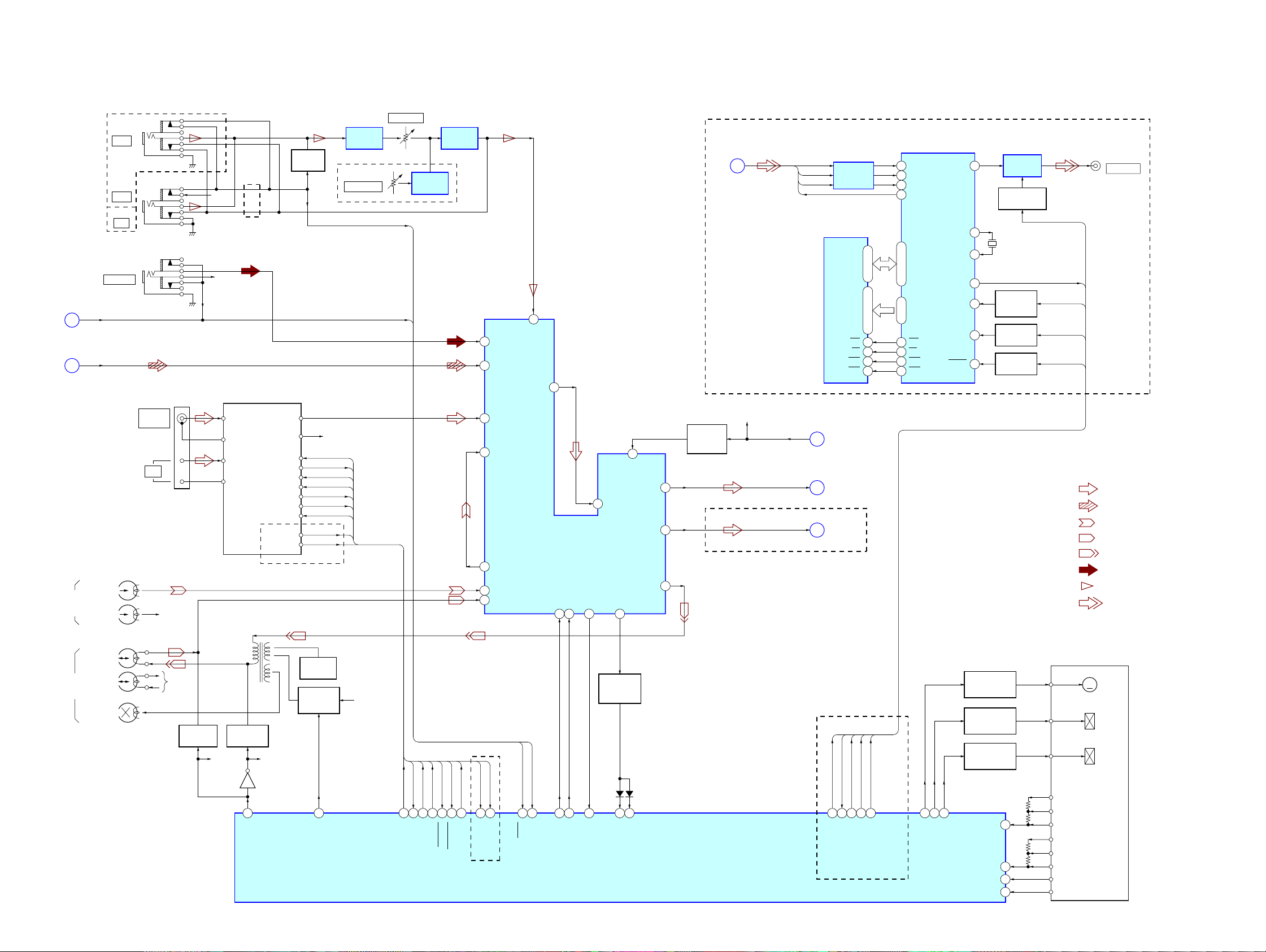
HCD-GX355/GX555/RG270/RG475/RG575
Ver. 1.1
6-2. BLOCK DIA GRAM – A UDIO/VIDEO Section –
(Page 23)
(Page 21)
E
A
HP1
(PB)
(DECK-A)
(MX)
JK801
MIC 1
JK802
MIC 2
JK802
MIC
(E2, E51, AR)
J751
AUDIO IN
HP IN
CD-L
L-CH
R-CH R-CH
FM 75Ω
COAXIAL
AM
+9V
(E2, E51, AR)
R-CH
FM/AM TUNER PACK
FM ANT
ANT GND
AM ANT
ANT GND
LC72121 DI
LC72121 DO
LC72121 CLK
LC72121 CE
BIAS OSC
L201
TUNER-L
TUNER-R
TUNED
STEREO
TU MUTE
RDS DATA
RDS CLK
MUTING
Q801
TU-MUTING
(AEP, UK, EE)
R-CH
CLK
TUNED
STEREO
R-D
R-C
MIC AMP
IC801 (1/2)
ECHO LEVEL
DO
DI
CE
VR851
MIC LEVEL
MIC IN
HP/AUX IN
VR801
ECHO AMP
IC802
MIC AMP
IC801 (2/2)
(MX)
63
1
61
3
7
9
11
MD L
CD L
TUNER L
TAPE L
PB OUT1
TAPE A1
TAPE B1
58
MIC
TONE OUT1
37
36
INPUT SELECT,
TONE CONTROL,
ELECTRICAL VOLUME
IC101
SI
AMS OUT
SC
19
40
18
VIN1
SAOUT1
55
35
BBIN1
VOL OUT1
SW OUT
REC OUT1
(MX)
DBFB
VOL OUT1
SW OUT
SBSO
WFCK
SCOR
EXCK
G
C
D
SCHMIT
TRIGGER
IC1005
D-RAM
IC1002
DQ1 – DQ4
A0 – A7
WE
OE
RAS
CAS
(Page 23)
(Page 23)
(Page 23)
1, 2, 24, 259 – 12, 14 – 17
3
22
4
23
B
(Page 21)
R-CH
FEED BACK
SWITCH
Q141
33
25
(GX555/RG475/RG575)
CD GRAPHICS
DECODER
IC1001
6
VIDEO AMP
VIDEO MUTING
X1002
14.31818 MHz
NTSC/PAL
SWITCH
Q1001
LEVEL SHIFT
Q1005, 1009
LEVEL SHIFT
Q1002, 1006
3
5
4
2
25, 27, 29, 3015 – 22
13
28
14
26
DATA
SFSY
SBSY
CLCK
VD0 – VD3
VA0 – VA 7
WE
OE
RAS
CAS
VOUT
XO1
GDET
DEN
MUTE
RESET
44
5960XI1
37
52
54
• Abbreviation
AR : Argentine model
E2 : 120V AC Area in E model
E51 : Chilean and Peruvian models
EE : East European model
MX : Mexican model
• R-ch is omitted due to same as L-ch.
IC1006
Q1010
J803
VIDEO OUT
VMUTE
CDG-DET
CDG/_BGC
MUTE_DATA
CDG-RST
• SIGNAL PATH
: TUNER
: CD PLAY
: TAPE PLAY (DECK-A)
: TAPE PLAY (DECK-B)
: REC
: AUX IN
15
: MIC
: VIDEO
L-CH
HRPE1
(REC/PB/ERASE)
(DECK-B)
R-CH R-CH
ERASE
PB MUTING
Q209
R-CH
REC MUTING
Q205, 207
HCD-GX355/GX555/RG270/RG475/RG575
Q203
90
O-REC/PB
R-CH
BIAS OSC
Q201
REC BIAS
SWITCH
Q231, 232
91
O-BIAS
+9V
DI
DO
CLK
66
65
67
I-LC72121-DI
O-LC72121-DO
O-LC72121-CLK
CE
TUNED
STEREO
68
69
70
I-TUNED
I-STEREO
O-LC72121-CE
R-D
TU-MUTING
71
72
O-ST-MUTE
(AEP, UK, EE)
R-C
18
I-RDS-CLK
I-RDS-DATA
MIC IN
HP/AUDIO IN
82
81
I-MIC
I-HP/AUDIO IN
1
2
92
O-BD3401-CLK
O-BD3401-DATA
BAND-PASS
FILTER
Q111, 112
D923 D921
93
94
I-VACS
I-STREAM
I-TAPE-AMS
SYSTEM CONTROLLER
IC901 (2/4)
2222
(MX)
VMUTE
63
60
O-VMUTE
CDG-DET
CDG/_BGC
59
I-CDG-DET
I-CDG-BGC
MUTE_DATA
57
CDG-RST
58
0-CDG-RST
I-CDG-MUTE-DATA
86
85
O-MOTOR
87
O-B-SOL
O-A-SOL
CAPSTAN/REEL
MOTOR DRIVE
Q341, 342
PLUNGER DRIVE
(DECK-A)
Q345, 346
PLUNGER DRIVE
(DECK-B)
Q343, 344
I-TAPE-A-STAT
I-TAPE-B-STAT
I-REEL-A
I-REEL-B
TAPE MECHANISM
DECK BLOCK
MM
(CAPSTAN/REEL)
(DECK-A)
(DECK-B)
A-HALF
A-MODE
88
89
83
84
REC (REW)
B-HALF
B-MODE
REC (FWD)
A-PHOTO
B-PHOTO
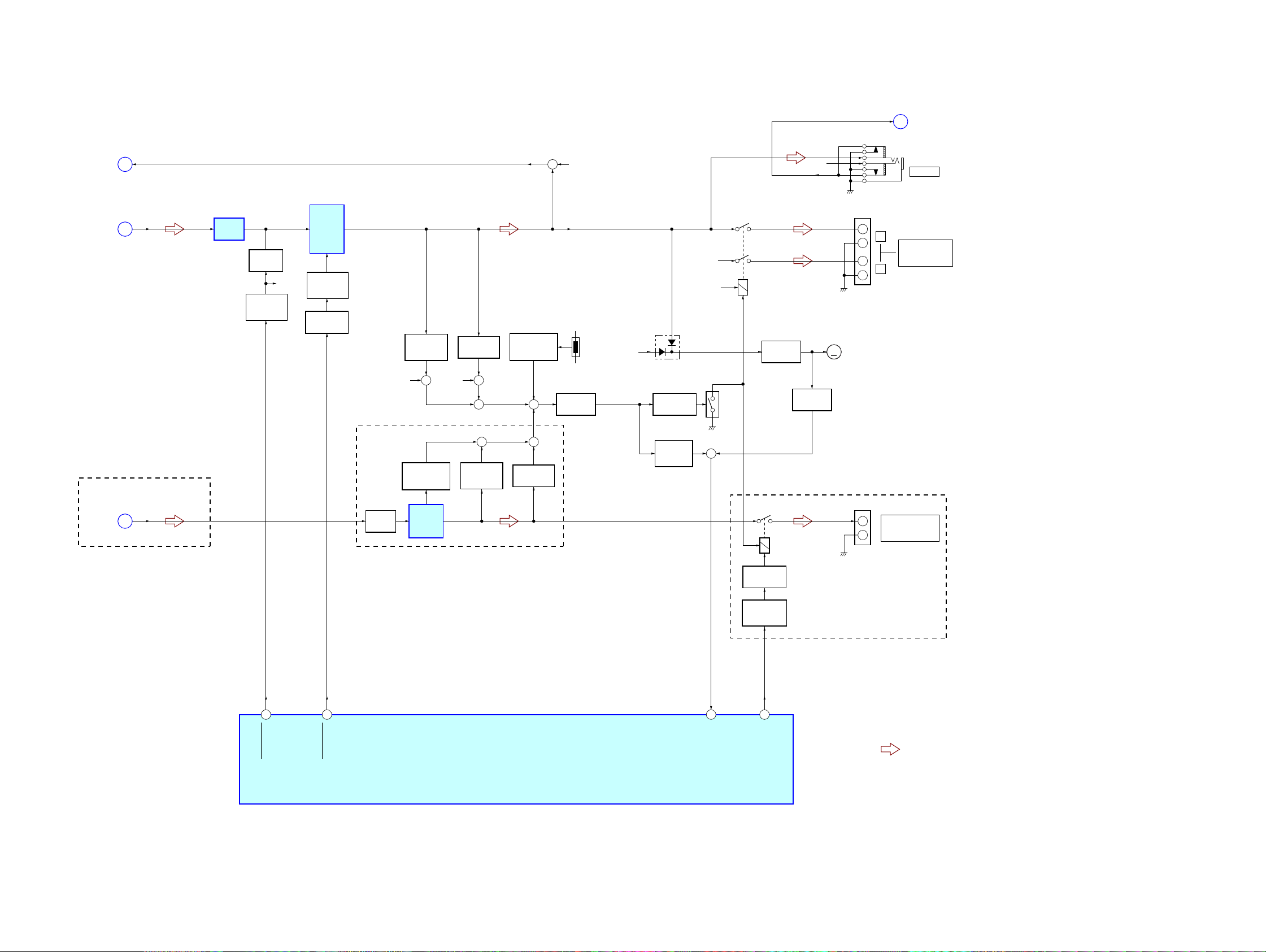
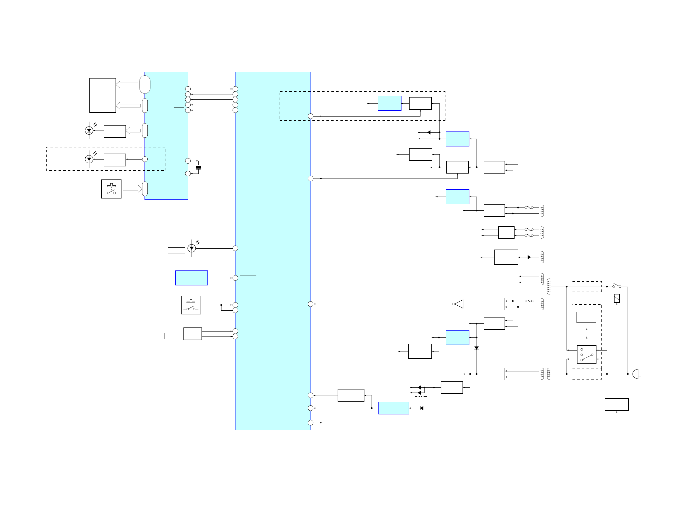
6-3. BLOCK DIAGRAM – AMP Section –
HCD-GX355/GX555/RG270/RG475/RG575
(Page 22)
(Page 22)
(GX555/RG475/RG575)
G
C
D
(Page 22)
DBFB
VOL OUT1
SW OUT
BUFFER
IC251
MUTING
Q251
MUTING
CONTROL
Q261
R-CH
POWER
AMP
IC441
STANDBY
SWITCH
Q489
AMP ON/OFF
Q933
OVER LOAD
DETECT
R-CH
(GX555/RG475/RG575)
TEMPERATURE
DETECT
Q503, 507
BUFFER
Q271
Q441
+
POWER
AMP
IC501
R-CH
DC DETECT
Q481, 482
+
+
+
OVER LOAD
DETECT
Q501
TEMPERATURE
DETECT
Q483, 484
+
+
DC DETECT
Q505, 506
+
PROTECTOR
R-CH
TH441
Q485
R-CH
D035
RELAY DRIVE
Q486
PROTECT
DETECT
Q487
R-CH
RY B+
RELAY SWITCH
Q488
+
RY441
FAN ON/OFF
Q044
RY501
R-CH
FAN DETECT
Q045
HP IN
JK441
+
–
+
–
M001
MM
(FAN)
JK501
+
–
(Page 22)
E
PHONES
L
FRONT SPEAKER
IMPEDANCE
USE 6 – 16Ω
R
SUB WOOFER OUT
IMPEDANCE
USE 6 – 16Ω
J701
23
O-SYS-MUTE
24
O-STK-MUTE
SYSTEM CONTROLLER
IC901 (3/4)
95
I-PROTECTOR
RELAY DRIVE
Q502
SUB WOOFER
ON/OFF
Q274
25
O-SWR
(GX555/RG475/RG575)
• R-ch is omitted due to same as L-ch.
• SIGNAL PATH
: TUNER
HCD-GX355/GX555/RG270/RG475/RG575
2323
HCD-GX355/GX555/RG270/RG475/RG575
Ver. 1.1
6-4. BLOCK DIAGRAM – PANEL, POWER SUPPLY Section –
D601 – 606
(FRONT PANEL LED)
(GX555/RG475/RG575)
D608
(FRONT PANEL LED)
FLUORESCENT
S611 – 617,
S621 – 626,
S631 – 638,
S641 – 648,
SW601
FL701
INDICATOR
TUBE
LED DRIVE
Q601 – 606
LED DRIVE
Q608
FL/LED DRIVER
S1 – S21
61 – 67
45 – 58,
G1 – G13
68 – 80
STREAN LED1
– STREAN LED6
26 – 31
32
SW LED
KEY1 – KEY4
19 – 22
IC701
SO1
X2
X1
D611
STANDBY
SYSTEM CONTROLLER
IC901 (4/4)
• Abbreviation
E2 : 120V AC Area in E model
E3 : 240V AC Area in E model
E51 : Chilean and Peruvian models
EA : Saudi Arabia model
MX : Mexican model
MAIN POWER
TRANSFORMER
PT901
F907
F904
F905
D908
D301, 302
RY B+
+9V
(MX)
+9V
REGULATOR
IC021
B+ SWITCH
Q041, 042
+9V
REGULATOR
IC011
+16V
AMP B+
AMP B–
VP
RECT
D021 – 024
RECT
D011 – 014
REGULATOR
RECT
D401
B–
Q902
9
8SI1
7SCK1
16CE
6RESET
4
X701
4.19MHz
3
36 I-VFD-DATA
35 O-VFD-DATA
37 O-VFD-CLK
4 O-VFD-CE
3 O-VFD-RESET
22
O-STBY-LED
O-CDG-POWER
O-FRONT-SP-RELAY
CDG +5V
61
27
+5V
REGULATOR
IC1003
FAN B+
B+ SWITCH
Q1007, 1008
M+7V
M+9V
REGULATOR
Q043
S601, 602
S660
VOLUME
REMOTE CONTROL
RECEIVER
IC610
ROTARY
ENCODER
I-SIRCS-IN
7
74 I-KEY0
97 I-POWER, DISPLAY
6 I-VOL-A
21 I-VOL-B
I-AC-PULSE
I-RESET
I-AC-CUT
O-POWER-RELAY
VF1
VF2
20
+3.3V
MP3 +1.5V
12
5
26
RESET SWITCH
Q901
VREF, VDD
VOLTAGE DETECT
IC902
+1.5V
REGULATOR
IC303 (EXCEPT MX)
IC303 (MX)
D902
VCC
D903
Q902
UNREG
+3.3V
REGULATOR
IC006
EVER +10V
REGULATOR
Q903, 904
D007, 008
D001 – 004
D006
D902 – 905
RECT
RECT
RECT
F906
SUB POWER
TRANSFORMER
PT902
(EXCEPT E2, E3, E51, EA)
(E2, E3, E51, EA)
S901
VOLTAGE
SELECTOR
240V
220V
120V
(EXCEPT E2, E3, E51, EA)
RY901
RELAY DRIVE
Q002
W001
(AC IN)
HCD-GX355/GX555/RG270/RG475/RG575
2424
HCD-GX355/GX555/RG270/RG475/RG575
d
Ver. 1.1
• Note For Printed Wiring Boards and Schematic Diagrams
Note on Printed Wiring Board:
• X : parts extracted from the component side.
• Y : parts extracted from the conductor side.
• f : internal component.
• : Pattern from the side which enables seeing.
(The other layers' patterns are not indicated.)
Caution:
Pattern face side: Parts on the pattern face side seen from
(Conductor Side) the pattern face are indicated.
Parts face side: Parts on the parts face side seen from
(Component Side) the parts face are indicated.
Caution:
Pattern face side: Parts on the pattern face side seen from
(Side B) the pattern face are indicated.
Parts face side: Parts on the parts face side seen from
(Side A) the parts face are indicated.
• Indication of transistor
C
Q
B
B
E
Q
CE
These are omitted.
These are omitted.
Note on Schematic Diagram:
• All capacitors are in µF unless otherwise noted. (p: pF)
50 WV or less are not indicated except for electrolytics
and tantalums.
• All resistors are in Ω and 1/
specified.
• f : internal component.
• 2 : nonflammable resistor.
• 5 : fusible resistor.
• C : panel designation.
Note:
The components identified by mark 0 or dotted
line with mark 0 are critical for safety.
Replace only with part
number specified.
• A : B+ Line.
• B : B– Line.
• Voltages and waveforms are dc with respect to ground
under no-signal conditions.
– CD/BD Section –
no mark :CD PLAY
– CD-G Section –
no mark : CD-G PLAY
– Other Sections –
no mark : FM
(): CD PLAY
〈〈 〉〉 : TAPE PLAY
[]: T APE REC
∗ : Impossible to measure
• Voltages are tak en with a V OM (Input impedance 10 MΩ).
Voltage variations may be noted due to normal production tolerances.
• Waveforms are taken with a oscilloscope.
Voltage variations may be noted due to normal production tolerances.
• Circled numbers refer to waveforms.
• Signal path.
F : TUNER (FM/AM)
E : TAPE PLAY (DECK A)
d : TAPE PLAY (DECK B)
G : REC
J : CD PLAY
f : AUX IN
N : MIC
L : VIDEO
• Abbreviation
AR : Argentine model
AUS: Australian model
CND : Canadian model
E2 : 120 V AC Area in E model
E3 : 240 V AC Area in E model
E51 : Chilean and Peruvian models
EA : Saudi Arabia model
EE : East European model
MX : Mexican model
RU : Russian model
SP : Singapore model
4
W or less unless otherwise
Note:
Les composants identifiés par
une marque 0 sont critiques
pour la sécurité.
Ne les remplacer que par une
pièce portant le numéro
spécifié.
• Circuit Boards Location
SW board
MOTOR (LD) board
MIC board
(E2, E51, MX)
TRANSFORMER board
PANEL board
VOL board
CD-G board (MX)
SUB TRANS board
AC1 board
BD board (MX)/
CD board (EXCEPT MX)
SENSOR board
DRIVER board
MOTOR (TB) boar
VIDEO OUT board (MX)
MAIN board
SUB WOOFER board
(GX555/RG475/RG575)
HCD-GX355/GX555/RG270/RG475/RG575
POWER board
AUDIO IN board
HEADPHONE board
MAIN board
2525
HCD-GX355/GX555/RG270/RG475/RG575
Ver. 1.1
6-5. PRINTED WIRING BOARD – CD Board – (Except MX model)
1 2 3 4 5 6 7 8 9
A
CD BOARD
(COMPONENT SIDE)
R121
C123
C195
R352
R353
C501
R501
B
C
D
FB301
R201
R205
C201
C203
C302
C303
C305
C210
R313
C315
C316
C314
C312
R162
165
R
171
X
405
R
351
R
R354
R302
C308
R191
173
R
C174
C196
C172
R172
171
171
C
R
C134
C125
C318
C184
C183
C182
C209
C151
• See page 25 for Circuit Boards Location.
C255
IC501
C257
C258
C259
C14
C10
C15
11
12
R
C18
R
C11
C16
R13
Q10
R10
E
C260
R253
C116
C12
C13
C17
1-860-502-
: Uses unleaded solder.
CD BOARD
(CONDUCTOR SIDE)
C252
IC251
R252
C251
TP (VC)
113
C
R
113
C112
C111
114
R
TP (FE)
PICK-UP BLOCK
112
R
CN101
OPTICAL
(KSM-215DCP)
C114
251
R
13
(13)
C320
C115
R111
M101
(SPINDLE)
M
S101
(LIMIT)
R411
C307
C309
C122
TP (RFACO)
C306
17
307
R
IC301
32
R303
R407
IC101
C124
R132
C163
IC303
13
54
R404
R403
R419
C313
116
4833
C310
C212
R163
132
133
C
C
141
R
143
R133
R
131
C131
R
R301
64
R306
49
R409
C211
C143
R142
C141
C142
C311
C317
R305
R402
R401
213
C
410
R
408
R
412
C194
R
406
R
182
R
C181
C162
181
C161
151
R
R203
R
161
R
M102
M
(SLED)
186
C
R204
C185
CN201
CN202
1-860-502-
MAIN BOARD
A1
CN301
(Page 32)
13
(13)
E
HCD-GX355/GX555/RG270/RG475/RG575
2626
HCD-GX355/GX555/RG270/RG475/RG575
Ver. 1.1
6-6. SCHEMATIC DIAGRAM – CD Board – (Except MX model)
R307
C307
10k
0.1
MP3REQ
R303
100k
C310
0.1
(Page 35)
FB301
C314
TP433
MP3VDD
WE/SDO1
SDO2
CS/RAS/
PO12
AD15/CAS/
PIO7/BUS3/IO7
SDO3/OE
PO9/AD12
PO08/AD11
VDDM
SRMSTB
VDDT
AD10
AD9
AD8
PO07/AD7
PO06/AD6
PO05
AD5/
47
4V
CN201
27P
M+7V
M-GND
M-GND
MP3-STB
MP3-REQ
MP3-ACK
MP3-CLK
MP3-DIO
MP3-LP
MP3-CS
MP3(3.3V)
MP3-RST
MP3-GND
SCOR
CD-SENS
CD-CLK
XLT
CD-DATA
XRST
XTCN
AVDD(3.3V)
R-CH
A-GND
L-CH
D-GND
DOUT
DVDD(3.3V)
PIO6/FI3/BUS2/IO7
PIO4/FI1/BUS0/IO4
PIO5/FI2/BUS1/IO5
PO11/BUCK/AD14
PO10/CCE/AD13
AD0/PO00
AD1/PO01
AD3/PO03
AD2/PO02
AD4/PO04
C312C313
C311 C309
0.10.1
0.1 0.1
VOUT
C305 TP422
C302 C303
220
0.1 0.1
4V
TP186
TP187
TP401
TP402
TP403
TP404
TP405
TP406
TP407
TP408
R205
TP417
TP416
TP415
TP414
TP413
TP412
TP419
TP434
TP410
TP411
TP409
R204
PIO3/IO3
PIO2/IO2
MP3 DECODER
TC94A34FG-002
VDD
VSS
C308
47
4V
STBY
NC
MVDD
MGND
MP3STB
MP3REQ
MIACK
MICK
MIDIO
MILP
MICS
MP3RST
0
SCOR
SENS
CLK
XLT
DATA
XRST
XTCN
AVDD
ROUT
LOUT
DOUT
PIO0/SDI2/IO0
PIO1/SDI3/IO1
IC301
VDDX
CKO/PO13/AD16
R306
VIN
GND
VSS
IRQ/FIO
XO
0
CKI/CLOCK/
XI
+1.5V REGULATOR
VDD
VSSX
IC303
BH15FB1WG
R411
R410
R409
R408
R407
R406
R412
TXO
TEST
SBSY/BCKIB
SFSY/LRCKIB
VSSP
MIMD
MP3GND
MP3STB
MP3REQ
MIACK
MIDIO
MP3RST
100
100
100
100
100
100
100
SDI1/
DATA
LRCKIA
BCKIA
SDI0
LRCKO
BCKO
SDO0
MICK
MILP
MICS
STANBY
VCOI
CLOCK
XTACN
MIACK
RESET
R313
VSS
VDDT
MICK
MIDIO
MILP
MICS
VDDP
220
C316C315
0.00220.1
SCOR
C212
SENS
22p
XLT
C211
DATA
220p
XRST
AOUT2
AOUT1
C306
R405
R404
R419
R403
R402
R401
R301
100k
R305
100k
C317
0.01
DOUT
• See page 50 for Waveforms. • See page 50 for IC Block Diagrams.
C142
C151
R203
0
R354
100
R352
100
R351
100
0.1
MIACK
100
MICK
100
MIDIO
MILP
100
MICS
100
MP3STB
100
MP3RST
100
C318
0.01
C213
22p
C320
0
TP435
DVDD
R353
100
10k
R302
R201
AVDD
TP436
C161
0.1
C181
0.1
0
R173
C185
470p
C182
0.1
C186
470p
C201
100
10V
AGND
TP420
C209
0.01
DOUT
C171 R171
22p 470
C172
27p
AOUT1
AOUT2
DGND
TP421
TP427
PCMDI
TP103
LRCK
TP104
PCMD
TP105
BCK
R161
100
C174X171
R172
1M
C183
R181
22
100
6.3V
C184
R182
22
100
6.3V
C203
C162
100
0.1
10V
BCKI
PCMDI
LRCKI
LRCK
VSS
PCMD
BCK
VDD
EMPH
EMPHI
IOVDD2
DOUT
TEST
TEST1
IOVSS2
NC
0.116.9344MHz
XVSS
XTAO
XTAI
XVDD
AVDD1
AOUT1
VREFL
AVSS1
AVSS2
VREFR
AOUT2
AVDD2
NC
IOVDD0
RMUT
LMUT
C501
IC501
TC7S08FU
C143
100
0.1
10V
R151
0
NC
DDCR
XTSL
NC
R165
0
0.1
R501
100
C141
R141
4.7k
AVSS5
VRSEN
AVDD5
DD
DDVROUT
SQCK
SQSO
IOVSS0
XTACN
R162
47k
C210
0.1
C194
0.1
N
C
TA
X
GND
VCCSWITCHING
100p
C133
0.01
R133
180k
R132
10k
VCTL
AVSS3
VSS
DATA
C196
0.1
A
T
T
A
L
X
D
MDP
C131
C125 R121
R131C134
0.1 15k
1M0.1
TP125
0.47
C132
BIAS
ASYI
ASYO
VPCO
CXD3059AR
XLAT
K
C
O
L
C
CD DSP
AVDD3
IC101
SCLK
SENS
VDD
CLOCK
R191
S
N
E
S
MOTOR/COIL
DRIVE
IC251
BA5947FM
TP
RFACI
(RFACO)
330p
C124
RFACI
AVSS4
RFACO
FCK
XUGF
W
ATSK
0
C122C123
0.10.1
LD
PD
NC
_IN
RFC
EG
VDD
SCOR
C2PO
GFS
XPCK
R
O
C
S
JPO004C251R252R251
MDP6800p22k10k
SW
PINO
OPIN+
OUTVREF
OPOUT
PREVCC
R
D
F
T
AC_SUM
C4M
R
D
R
T
CH1FIN
CH4CAPA
PDSENS
DCK
W
1RIN
CH
CH4IN
NC
AVDD4
RFDCO
D
C
B
A
VC
FEO
FEI
TEO
TEI
F
E
NC
AVSS0
AVDD0
IOVDD1
FRDR
FFDR
TRDR
TFDR
SRDR
SFDR
IOVSS1
SSTP
MDP
LOCK
VSS
FOK
DFCT
MIRR
COUT
NC
R
R
D
D
FR
FF
CH2FIN
CH2RIN
CH3FIN
CH3RIN
R
R
D
R
FD
S
S
1500p
R143
3.3k
0.1
1k
R142
FILI
PCO
FILO
CLTV
SYSM
XRST
EXCK
SBSO
0.1
100
C163
R163
T
S
R
X
JPO10 R11
APC 0
R253TP418
10kGAIN_SW
C259
0.1
TP423
IOP1
C17
220
4V
R111
1k
(FE)
TP
R113
1k
JPO103
TP428
TP429
TP430
TP431
TP425
TP432
GND
CNF4
MUTE
GND
AUTOMATIC
C18
1000p
R112
TEI
R114
FRDR
FFDR
TRDR
TFDR
SW+
MDP
F-
VCC
POW
VCC
POW
2SB1690K
POWER
CONTROL
2OUTR
CH
CH3OUTR
C16R12
F+T+T
1100k
Q10
15k
15k
TF
CH2OU
CH3OUTF
+
R13
R10
3.3
C111
C112
C113
C114
C115
0.1
T-
CH1OUTR
CH4OUTF
FRDR
FFDR
TRDR
TFDR
SRDR
SFDR
CH1OUTF
CH4OUTR
3300p
3300p
1
TP424
IOP2
D
C
B
A
470p
470p
F
E
MDP
C15
C10
0.1
10
E
C11
10
D
A
B
C
F
TP102
F+
C14
0.1
T-
C116
C195
0.1
C258
0.1
C257
0.1
C252
0.1
C255
0.1
C260
220
10V
F-
100
10V
TP
(VC)
SP-
TP250
SP+
TP251
SL+
TP252
SL-
TP253
VC
VCC
E
TP10
E
D
TP11
D
A
TP12
A
B
TP13
B
C
TP14
C
F
AGND
F
LD
VR
PD
TP15
PD
F+
TP16
F+
T+
TP17
F-
T-
TP18
T-
F-
TP19
F-
CN101
16P
TP426
SW-
S101
(LIMIT)
M101
(SPINDLE)
M102
(SLED)
HCD-GX355/GX555/RG270/RG475/RG575
2727
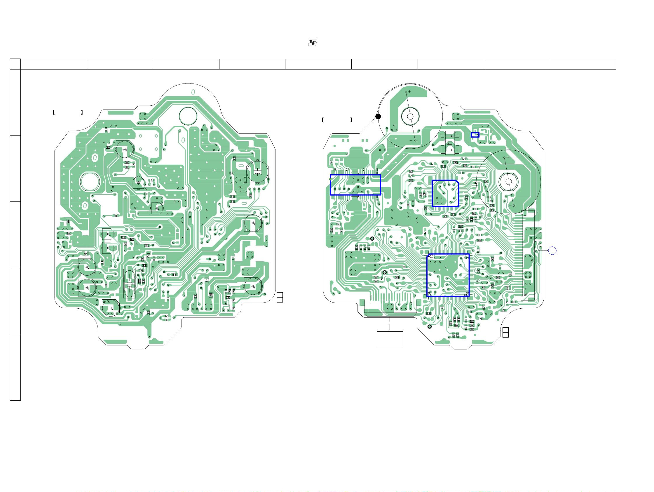
HCD-GX355/GX555/RG270/RG475/RG575
6-7. PRINTED WIRING BOARD – BD Board – (MX model only)
1 2 3 4 5 6 7 8 9
A
BD BOARD
(COMPONENT SIDE)
R162
C314
C174
R313
R302
C312
C308
R191
R173
C196
C172
R172
171
171
C
R
C134
C195
C125
R121
C123
D
B
C
FB301
R205
R201
C201
C203
C182
C184
C183
C303
C302
C209
C151
C318
X171
C305
C210
C315
C316
165
R
• See page 25 for Circuit Boards Location.
C255
C257
C260
C258
C259
C10
C15
C18
C11
C16
E
Q10
R253
C116
C14
12
11
R
R
C17
R13
R10
1-864-566-
: Uses unleaded solder.
M101
M
C320
R353
R354
R352
(SPINDLE)
C307
R351
17
R307
32
C309
R411
C122
TP (RFACO)
C306
16
IC301
124
C
S101
(LIMIT)
C310
R303
R407
IC101
132
R
R404
1
4833
R133
131
R
C133
R163
C163
C313
131
C
R405
64
49
R419
C132
13
IC303
54
R403
R301
R306
R406
R412
R408
R203
C213
C162
C194
C181
C161
R151
R401
1-864-566-
C317
R305
R402
R182
R161
C186
R181
R204
R423
11
(11)
C311
R410
R409
C211
C212
C143
141
R
R142
C141
143
R
C142
M102
M
(SLED)
CN201
C185
421
R
R422
A2
MAIN BOARD
CN301
(Page 32)
BD BOARD
(CONDUCTOR SIDE)
C251
IC251
C114
112
R
R111
CN101
OPTICAL
(KSM-215DCP)
C115
C113
113
R
TP (VC)
114
R
C112
C111
TP (FE)
PICK-UP BLOCK
C252
252
R
251
R
11
(11)
E
HCD-GX355/GX555/RG270/RG475/RG575
2828
 Loading...