

Page 1
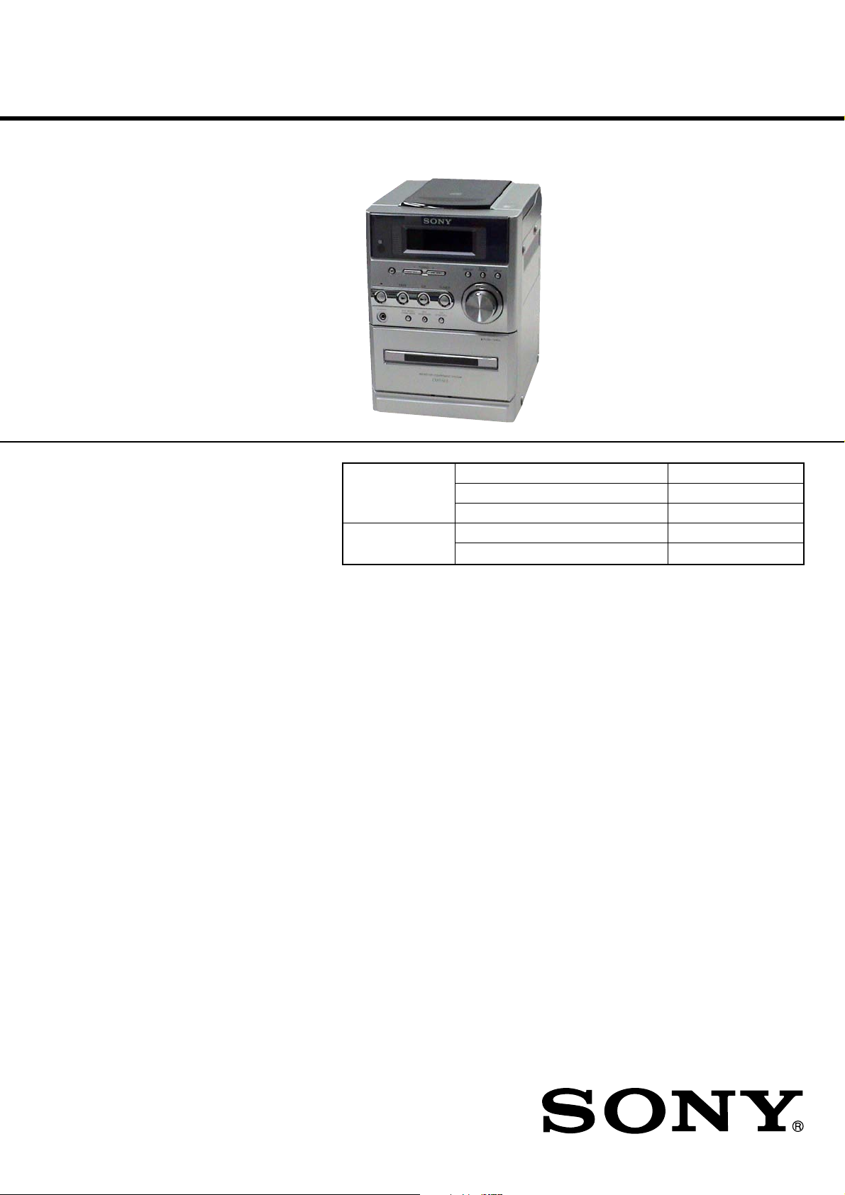
HCD-NE3
SERVICE MANUAL
Ver. 1.1 2005.07
• HCD-NE3 is the amplifier, CD player, tape deck
and tuner section in CMT-NE3.
CD Section Base Unit Name BU-K7BD80B
TAPE Section
US Model
Canadian Model
AEP Model
UK Model
E Model
Austr alian Model
Model Name Using Similar Mechanism NEW
Optical Pick-up Name KSM-213EDP/C2NP
Model Name Using Similar Mechanism NEW
Tape T ransport Mechanism Type CMAL5Z220A
AUDIO POWER SPECIFICATIONS
POWER OUTPUT AND TOTAL HARMONIC
DISTORTION:
(US model)
With 6 ohm loads, both channels driven, from
120-10,000 Hz; rated 13 watts per channel
minimum RMS power, with no more than 10%
total harmonic distortion from 250 milliwatts to
rated output.
Main unit
Amplifier section
North American model:
Continuous RMS power output (reference):
European model:
DIN power output (rated): 11 + 11 W (6 ohms at 1
Continuous RMS power output (reference):
Music power output (reference):
Other models:
The following measured at AC 230 V or AC 120 V, 50/
60 Hz
DIN power output (rated): 11 + 11 W
Continuous RMS power output (reference):
15 + 15 W
(6 ohms at 1 kHz, 10%
THD)
kHz, DIN)
15 + 15W (6 ohms at 1
kHz, 10% THD)
25 + 25 W
(6 ohms at 1 kHz, DIN)
15 + 15 W
(6 ohms at 1 kHz, 10%
THD)
SPECIFICATIONS
Inputs
MD (phono jacks): Sensitivity 450 mV,
Outputs
PHONES: Accepts headphones with
SPEAKER: Accepts impedance of 6 to
CD player section
Laser Semiconductor laser
Frequency response 20 Hz – 20 kHz
Wavelength 780 – 790 nm
Tape deck section
Recording system 4-track 2-channel, stereo
Frequency response 50 – 13,000 Hz (±3 dB),
impedance 47 kilohms
an impedance of 8 ohms or
more
16 ohms.
(λ=780 nm)
Emission duration:
continuous
using Sony TYPE I
cassettes
Tuner section
FM stereo, FM/AM superheterodyne tuner
FM tuner section
Tuning range 87.5 – 108.0 MHz
Antenna FM lead antenna
Antenna terminals 75 ohms unbalanced
Intermediate frequency 10.7 MHz
AM tuner section
US, Canadian, Mexican and Argentina models:
AEP and UK models: 531 – 1,602 kHz
Other models: 530 – 1,710 kHz
Antenna AM loop antenna, external
Intermediate frequency 450 kHz
530 – 1,710 kHz
(with the tuning interval
set at 10 kHz)
531 – 1,710 kHz
(with the tuning interval
set at 9 kHz)
(with the tuning interval
set at 9 kHz)
(with the tuning interval
set at 10 kHz)
531 – 1,602 kHz
(with the tuning interval
set at 9 kHz)
antenna terminal
General
Power requirements
US, Canadian and Mexican models:
AEP and UK models: 230 V AC, 50/60 Hz
Australian model: 230 – 240 V AC, 50/60 Hz
Argentina and Korean models:
Taiwanese model: 120 V AC, 50/60 Hz
Saudi Arabian model: 120 – 127/220 V AC, 50/
Other models: 110 – 120 V or 220 – 240 V
Power consumption 45 W
Dimensions (w/h/d) Approx. 164 × 230.5 × 263
Mass Approx. 3.7 kg
Supplied accessories Remote Commander (1)
Design and specifications are subject to change
without notice.
120 V AC, 60 Hz
220 V AC, 60 Hz
60 Hz
AC, 50/60 Hz
Adjustable with voltage
selector
mm incl. projecting parts
and controls
R6 (size AA) batteries (2)
AM loop antenna (1)
FM lead antenna (1)
9-877-693-02 Sony Corporation
2005G05-1 Personal Audio Group
© 2005.07 Published by Sony Engineering Corporation
COMPACT DISC DECK RECEIVER
Page 2
HCD-NE3
r
Notes on chip component replacement
•Never reuse a disconnected chip component.
• Notice that the minus side of a tantalum capacitor may be damaged by heat.
Flexible Circuit Board Repairing
•Keep the temperature of the soldering iron around 270 ˚C during repairing.
• Do not touch the soldering iron on the same conductor of the
circuit board (within 3 times).
• Be careful not to apply force on the conductor when soldering
or unsoldering.
CAUTION
Use of controls or adjustments or performance of procedures
other than those specified herein may result in hazardous radiation exposure.
The following caution label is located inside the unit.
This appliance is classified
CLASS 1 LASER PRODUCT
LUOKAN 1 LASER LAITE
KLASS 1 LASER APPARAT
as a CLASS 1 LASER
product.
This label is located on the
rear exterior.
SAFETY CHECK-OUT
After correcting the original service problem, perform the following safety check before releasing the set to the customer:
Check the antenna terminals, metal trim, “metallized” knobs,
screws, and all other exposed metal parts for AC leakage.
Check leakage as described below.
LEAKAGE TEST
The AC leakage from any exposed metal part to earth ground and
from all exposed metal parts to any exposed metal part having a
return to chassis, must not exceed 0.5 mA (500 microamperes.).
Leakage current can be measured by any one of three methods.
1. A commercial leakage tester, such as the Simpson 229 or RCA
WT -540A. Follo w the manufacturers’ instructions to use these
instruments.
2. A battery-operated AC milliammeter. The Data Precision 245
digital multimeter is suitable for this job.
3. Measuring the voltage drop across a resistor by means of a
VOM or battery-operated AC voltmeter. The “limit” indication is 0.75 V, so analog meters must have an accurate lowvoltage scale. The Simpson 250 and Sanwa SH-63T rd are examples of a passive VOM that is suitable. Nearly all battery
operated digital multimeters that have a 2 V A C range are suitable. (See Fig. A)
To Exposed Metal
Parts on Set
UNLEADED SOLDER
Boards requiring use of unleaded solder are printed with the leadfree mark (LF) indicating the solder contains no lead.
(Caution: Some printed circuit boards may not come printed with
the lead free mark due to their particular size)
: LEAD FREE MARK
Unleaded solder has the following characteristics.
• Unleaded solder melts at a temperature about 40 ˚C higher than
ordinary solder.
Ordinary soldering irons can be used but the iron tip has to be
applied to the solder joint for a slightly longer time.
Soldering irons using a temperature regulator should be set to
about 350 ˚C.
Caution: The printed pattern (copper foil) may peel away if the
heated tip is applied for too long, so be careful!
• Strong viscosity
Unleaded solder is more viscou-s (sticky, less prone to flow)
than ordinary solder so use caution not to let solder bridges occur such as on IC pins, etc.
• Usable with ordinary solder
It is best to use only unleaded solder but unleaded solder may
also be added to ordinary solder.
SAFETY-RELATED COMPONENT WARNING!!
COMPONENTS IDENTIFIED BY MARK 0 OR DOTTED
LINE WITH MARK 0 ON THE SCHEMATIC DIAGRAMS
AND IN THE PARTS LIST ARE CRITICAL TO SAFE
OPERATION. REPLACE THESE COMPONENTS WITH
SONY PARTS WHOSE PART NUMBERS APPEAR AS
SHOWN IN THIS MANUAL OR IN SUPPLEMENTS PUBLISHED BY SONY.
AC
1.5 k
0.15 µF
Fig. A. Using an AC voltmeter to check AC leakage.
ATTENTION AU COMPOSANT AYANT RAPPORT
À LA SÉCURITÉ!
LES COMPOSANTS IDENTIFIÉS P AR UNE MARQUE 0
SUR LES DIAGRAMMES SCHÉMA TIQUES ET LA LISTE
DES PIÈCES SONT CRITIQUES POUR LA SÉCURITÉ
DE FONCTIONNEMENT. NE REMPLACER CES COMPOSANTS QUE PAR DES PIÈCES SONY DONT LES
NUMÉROS SONT DONNÉS DANS CE MANUEL OU
DANS LES SUPPLÉMENTS PUBLIÉS PAR SONY.
Ω
Earth Ground
voltmete
(0.75 V)
2
Page 3

TABLE OF CONTENTS
1. SERVICING NOTES ................................................ 4
2. GENERAL
Location of Controls ....................................................... 6
3. DISASSEMBLY
3-1. Disassembly Flow ........................................................... 8
3-2. Rear Cabinet .................................................................... 8
3-3. Top Panel Assy ................................................................ 9
3-4. Front Panel Assy ............................................................. 9
3-5. Base Unit (BU-K7BD80B) ............................................. 10
3-6. Mechanical Deck ............................................................. 10
3-7. MAIN Board ................................................................... 11
3-8. AMP Board ..................................................................... 11
4. TEST MODE.............................................................. 12
5. ELECTRICAL CHECK .......................................... 14
6. DIAGRAMS
6-1. Block Diagram – CD SERVO Section – ....................... 15
6-2. Block Diagram – MAIN Section – ................................ 16
6-3. Note for Printed Wiring Boards
and Schematic Diagrams ................................................ 17
6-4. Printed Wiring Board – BD Board – ............................. 18
6-5. Schematic Diagram – BD Board – ................................ 19
6-6. Printed Wiring Boards – MAIN Section – .................... 20
6-7. Schematic Diagram – MAIN Section – ......................... 21
6-8. Printed Wiring Boards – AMP Section –....................... 22
6-9. Schematic Diagram – AMP Section – ........................... 23
6-10. Printed Wiring Boards – PANEL Section – .................. 24
6-11. Schematic Diagram – PANEL Section –....................... 25
6-12. Printed Wiring Board – POWER Board –..................... 26
6-13. Schematic Diagram – POWER Board –........................ 27
HCD-NE3
7. EXPLODED VIEWS
7-1. Panel Section ................................................................... 32
7-2. Front Panel Assy-1 .......................................................... 33
7-3. Front Panel Assy-2 .......................................................... 34
7-4. Top Panel Assy ................................................................ 35
8. ELECTRICAL PARTS LIST ............................... 36
3
Page 4
HCD-NE3
SECTION 1
SER VICING NOTES
NOTES ON HANDLING THE OPTICAL PICK-UP
BLOCK OR BASE UNIT
The laser diode in the optical pick-up block may suffer electrostatic break-down because of the potential difference generated
by the charged electrostatic load, etc. on clothing and the human
body.
During repair, pay attention to electrostatic break-down and also
use the procedure in the printed matter which is included in the
repair parts.
The flexible board is easily damaged and should be handled with
care.
NOTES ON LASER DIODE EMISSION CHECK
The laser beam on this model is concentrated so as to be focused
on the disc reflective surface by the objective lens in the optical
pick-up block. Therefore, when checking the laser diode emission, observe from more than 30 cm away from the objectiv e lens.
• MODEL IDENTIFICATION
– Rear Cabinet –
Power Voltage Indication
MODEL Pow er V oltage Incdication
US, Canadian, Mexican and
models
AEP and UK models AC: 230 V - 50/60 Hz 45 W
Australian model AC: 230 – 240 - 50/60 Hz 45 W
Argentina and Korean models AC: 220 V - 60 Hz 45 W
Taiwan model AC: 120 V 50/60 Hz 45 W
Saudi Arabia model
Other models
AC: 120 V 60 Hz 45 W
AC: 120 – 127/220 V
50/60 Hz 45 W
AC: 110 – 120/220 – 240 V
50/60 Hz 45 W
NOTE ON LEADING THE WIRE (FLAT TYPE)
• In order to separate wire (flat type) from no shield portion of TC wire, stick filament tapes, as shown in a figure.
TC wire (no shield portion)
main board
filament tape
wire (flat type)
4
Page 5
SERVICE POSITION
– BD board –
HCD-NE3
BD board
– TCM block –
– AMP board –
TCM block
AMP board
5
Page 6
HCD-NE3
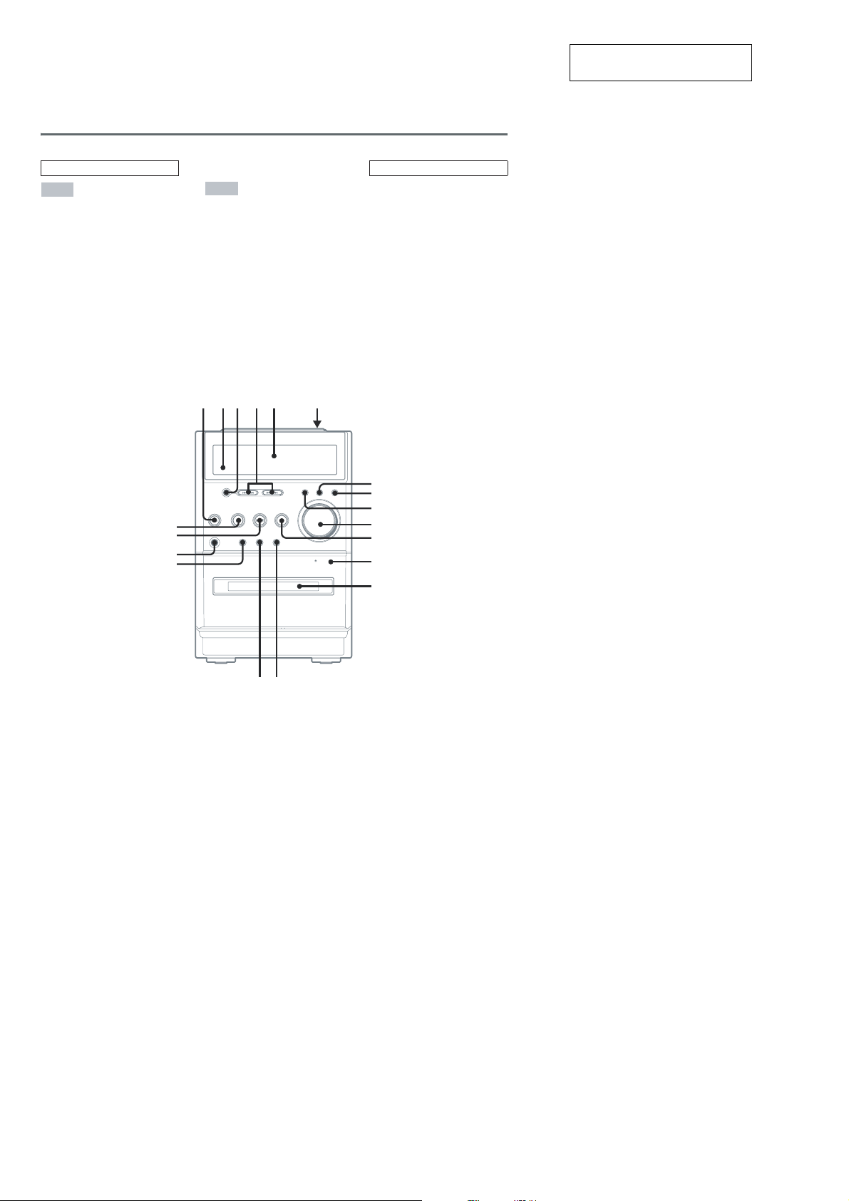
• LOCATION OF CONTROLS
Main unit
ALPHABETICAL ORDER
A – O
BASS/TREBLE 8
Cassette compartment qf
CD SYNCHRO qg
DISPLAY 0
Displaywindow 5
DSGX 9
P – Z
PHONES jack qk
PLAY MODE qj
Remote sensor 2
TUNER/BAND qs
TUNING +/− 4
TUNING MODE qj
VOLUME qa
12345 6
SECTION 2
GENERAL
BUTTON DESCRIPTIONS
?/1 (power) 1
.m/M> (skip back/
skip forward,rewind/fast
forward) 4
x (stop) 3
z RECPAUSE/START qh
CD/NX(play/pause) ql
TAPE/N(play) w;
Z PUSHOPEN/CLOSE (CD
open/close) 6
Z PUSHOPEN (tape open/close)
qd
This section is extracted from
instruction manual.
w;
ql
qk
qj
8
9
0
qa
qs
qd
qf
qgqh
6
Page 7
HCD-NE3
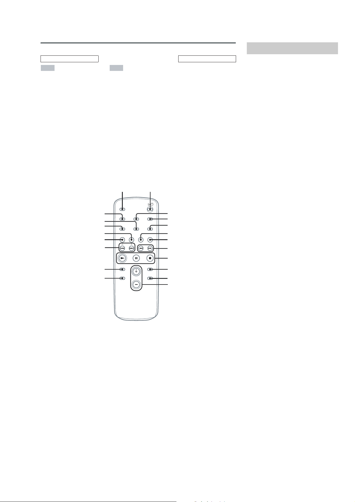
Remote control
ALPHABETICAL ORDER
A – O P – Z
CD qh
CLEAR qd
CLOCK/TIMER SELECT 2
CLOCK/TIMERS ET 3
DISPLAY ql
ENTER 9
EQ qs
FM MODE 4
FUNCTION 6
PLAY MODE qk
REPEAT 4
SLEEP w;
TAPE qg
TUNER/BAND 5
TUNER MEMORY qj
TUNING MODE qk
VOLUME +/− 0
ql
qk
qj
qh
qg
qf
CMT-NE3
w; 1
BUTTON DESCRIPTIONS
?/1 (power) 1
m/M (rewind/fast forward)
7
./> (go back/go forward)
qf
x (stop) 8
X (pause) 8
N (play) 8
+/− (tuning) qf
2
3
4
5
6
7
8
Setting the clock
Use buttons on the remote for the operation.
1
Press ?/1 to turn on the system.
2
Press CLOCK/TIMER SET.
3
Press ./> repeatedly to set the
hour.
4
Press ENTER.
5
Press ./> repeatedly to set the
minute.
6
Press ENTER.
The clock starts working.
To adjust the clock
1
Press CLOCK/TIMER SET.
2
Press ./> until “CLOCK” appears,
then press ENTER.
3
Do the same procedures as step 3 to 6
above.
Note
The clock is not displayed in Power Saving Mode.
qd
9
qs
0
* Button does not function with this model.
*
7
Page 8
HCD-NE3
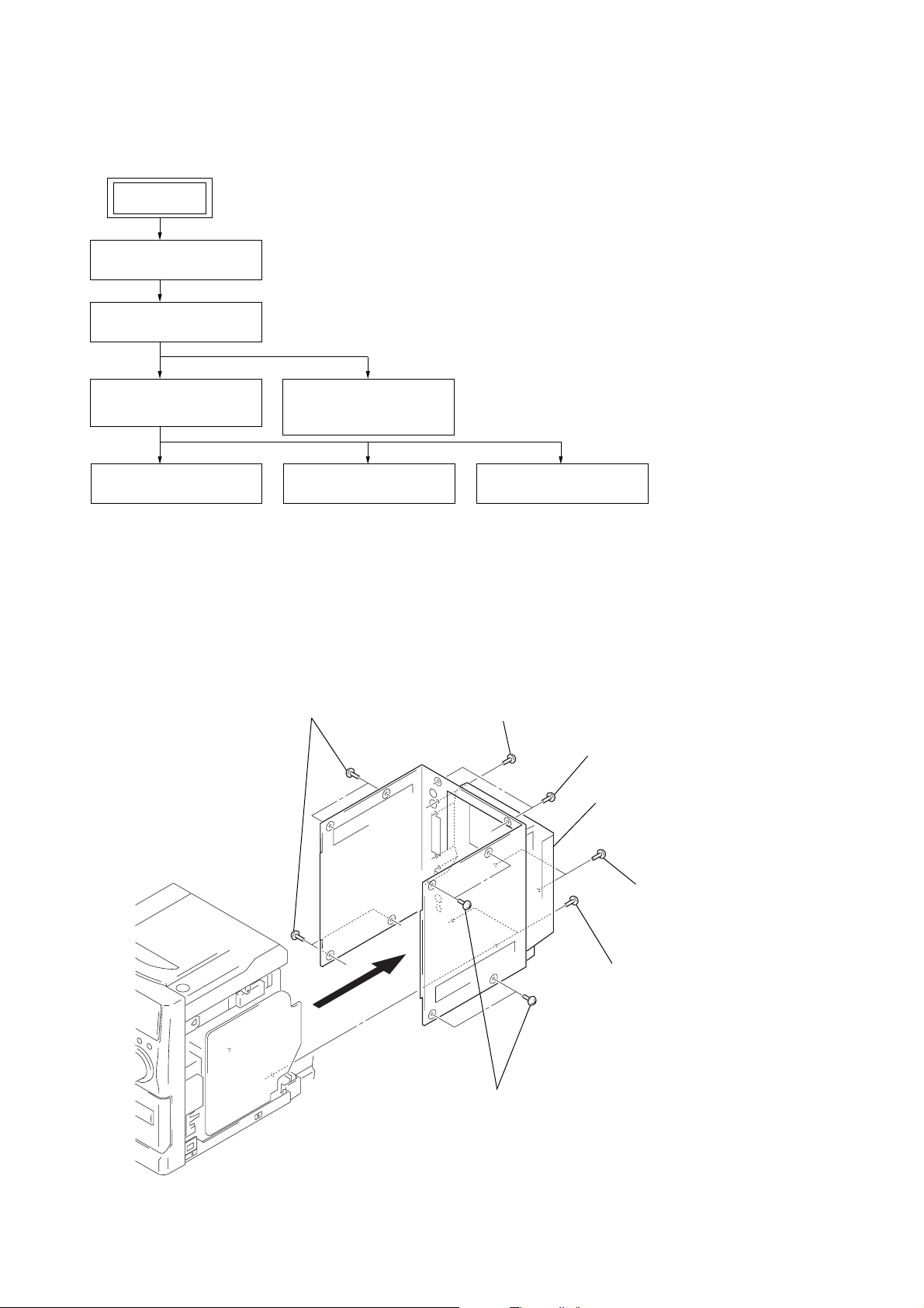
• This set can be disassembled in the order shown below.
3-1. DISASSEMBLY FLOW
SET
3-2. REAR CABINET
(Page 8)
3-3. TOP PANEL ASSY
(Page 9)
SECTION 3
DISASSEMBLY
3-4. FRONT PANEL ASSY
(Page 9)
3-6. MECHANICAL DECK
(Page 10)
Note: Follow the disassembly procedure in the numerical order given.
3-5. BASE UNIT
(BU-K7BD80B)
(Page 10)
3-7. MAIN BOARD
(Page 11)
3-2. REAR CABINET
1
four screws
(BVTP3 × 8)
3-8. AMP BOARD
4
five screws
(BVTP3
(Page 11)
×
10)
3
two screws
(BVTP3
7
×
10)
rear cabinet
6
two screws
(BVTP3 × 10)
5
two screws
(BVTP3 × 10)
2
four screws
(BVTP3 × 8)
8
Page 9
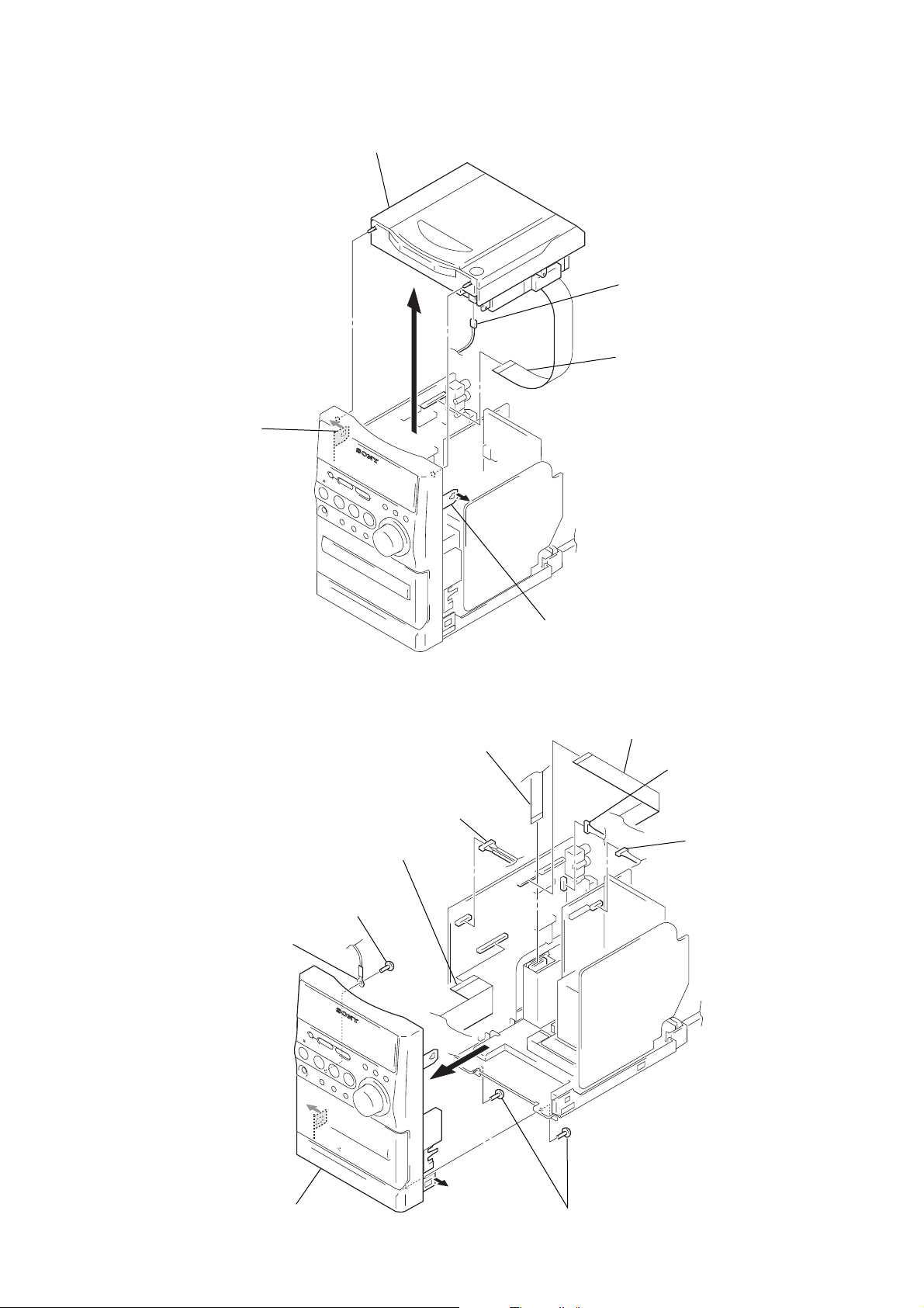
r
3-3. TOP PANEL ASSY
6
top panel assy
5
connector
(S820)
HCD-NE3
2
claw
3-4. FRONT PANEL ASSY
1
3
q;
wire (flat type) (11 core)
5
connector
(CN301)
wire (flat type) (19 core)
(CN302)
1
4
claw
2
wire (flat type) (8 core)
(CN303)
wire (flat type) (17 core)
(CN305)
3
connector
(CN309)
4
connecto
(CN501)
qs
harness
qd
qa
screw (2.6 × 10)
8
flont panel assy
7
9
6
two screws
(BVTP3
×
10)
9
Page 10
HCD-NE3
)
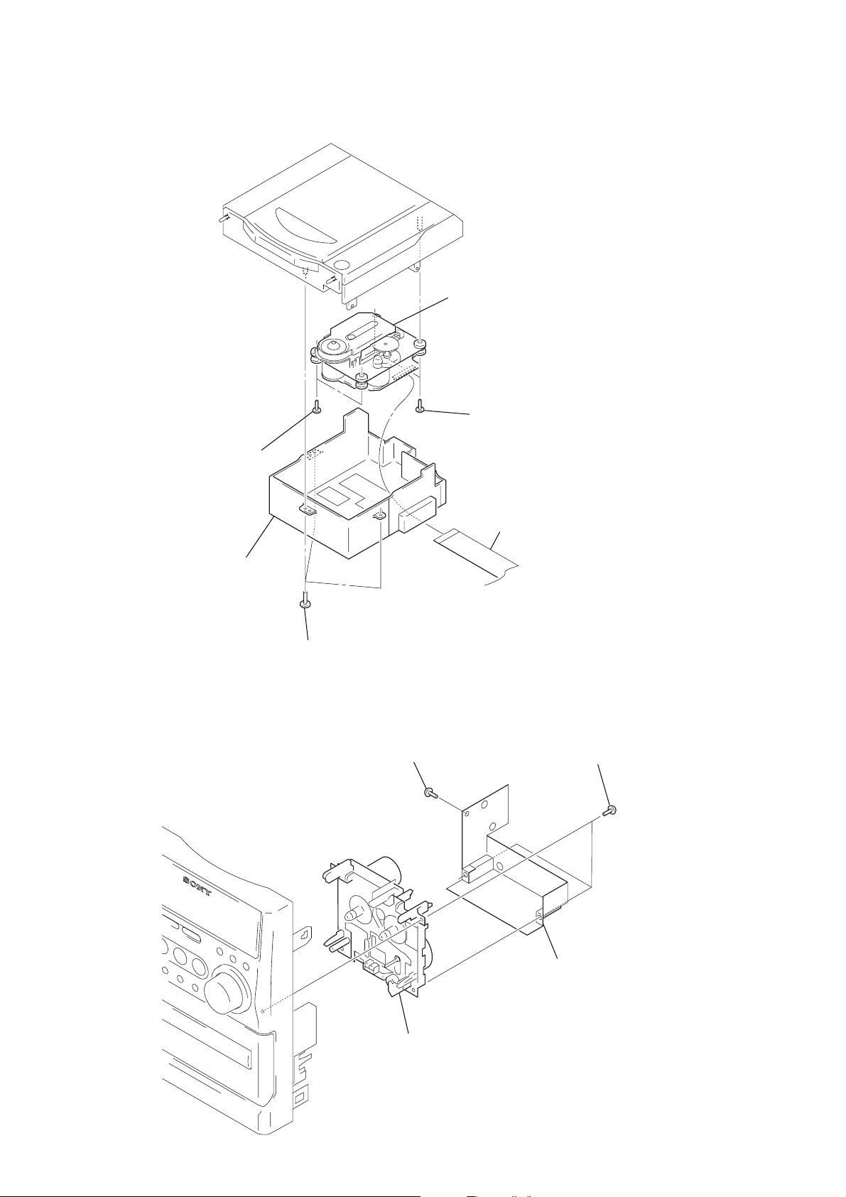
3-5. BASE UNIT (BU-K7BD80B)
5
two screws
×
10)
(2.6
6
base unit
(BU-K7BD80B)
4
two screws
(2.6
×
10)
2
CD cover
3-6. MECHANICAL DECK
1
three screws
(BVTP2.6
×
8)
2
screw
(BVTT2.6
3
wire (flat type) (17core)
(CN201)
1
three screws
×
10)
×
6)
(2.6
10
4
mechanical deck
3
shield (TC
Page 11
3-7. MAIN BOARD
)
4
two screws
(BVTP3 × 10)
6
5
main board
tuner (FM/AM)
1
connector (CNB308)
3
connector (CNB307
HCD-NE3
3-8. AMP BOARD
4
AMP board
2
connector (CN902)
3
two screws
(BVTP3
×
10)
1
connector (CNB308)
2
connector (CNB307)
11
Page 12
HCD-NE3
SECTION 4
TEST MODE
COLD RESET
* The cold reset clears all data including preset data stored in
the RAM to initial conditions. Execute this mode when returning the set to the customer.
Procedure:
1. Press the I/1 button to turn the power on.
2. While pressing the x button, press the I/1 button and turn
the [VOLUME] knob in the counter-clock wise.
3. The message “RESET” is displayed and the set is reset.
PANEL TEST
* All segments of liquid crystal display are tested, and the ver-
sion and released date of the micro computer are displayed.
Procedure:
1. Press the I/1 button to turn the power on.
2. While pressing the [DISPLAY] button, press the I/1 button
and turn the [VOLUME] knob in the counter-clock wise.
Then all segments of liquid crystal display are turned on.
3. Press the [DSGX] button, the version and released date of the
micro computer are displayed.
example of display:
1209 V100
Version of micro computer
(In this case, version 100)
released date of micro computer
(In this case, released of December 9)
4. Press the [BASS/TREBLE] button, the model name and destination are displayed.
example of display:
N3 NA
destination
(In this case, North-American model)
model name
(In this case, HCD-NE3)
5. To exit from this mode, perform the “COLD RESET”.
CD ERROR CODE DISPLAY MODE
• When this mode is entered, optical pick-up error code is dis-
played with the 8-character format on the liquid crystal display.
Procedure:
1. Press the I/1 button to turn the power ON.
2. Press the CD N X button to select “CD”.
3. While pressing the [DISPLAY] button, press the [PLAY/MODE/
TUNING MODE] and turn the [VOLUME] knob in the counter-
clockwise.
4. When this mode is activated, CD error code is displayed on
the liquid crystal display.
5. Press the TUNING + M > and TUNING – . m buttons,
error history No. is changed.
The first digit from the left indicates:
The first digit from the left indicates which mode the error history
is. “D” is displayed on the liquid crystal display.
The second digit from the left indicates:
(Error history No. display)
The second digit from the left indicates which order the error history is. “0” indicates the latest error history, and each time the
number increases by one, the error history goes back to one-previous error.
The third and 4th digit from the left indicates:
(Error status display)
The third and 4th digit from the left indicates which error status is
indicated.
Display Status
01 Not focused (TOC read without a disc)
02 GFS NG (TOC read with a disc chucked)
03 Start operation time-over
04 Defocused continuously (Defocused during TOC
reading)
05 Q code not entered for specified time
06 Tracking not turned ON
07 Blank disc (Blank disc TOC read)
The 5th and 6th digit from the left indicates:
(Error step display)
The 5th and 6th digit from the left indicates which processing when
a trouble occurred
Display Contents
01 SHIP in progress
02 Power OFF in progress
03 Power ON in progress
04 Initialize in progress
05 Oscillation stopping
06 From oscillation stop, oscillation starting
07 Stopping
08 Stop operation is under way
09 Start operation in progress
0A TOC read in progress
0B Search operation is under way
0C Playback operation is under way
0D Pause operation is under way
0E Playback manual search operation is under way
0F Pause manual search operation is under way
The 7th and 8th digit from the left indicates:
The 7th and 8th digit from the left indicates which operation in
progress when a trouble occurred. (Step of each processing of the
5th and 6th digits is indicated)
5 REPEAT LIMIT CANCEL MODE
• Number of repeat for CD playback is 5 times when the repeat
mode is “REPEAT”. This mode is used to enables CD to repeat
playback for limitless times.
Procedure:
1. Press the I/1 button to turn the power ON.
2. Press the CD N X button to select “CD”.
3. While pressing the x button, press the [PLAY MODE/TUN-
ING MODE] and turn the [VOLUME] knob in the counter-
clockwise.
4. The message “NO LIMIT” is displayed on the liquid crystal
display momentarily, CD repeat 5 limit is cancelled.
12
Page 13

TUNER STEP CHANGE-OVER
* Either the 9 kHz step or 10 kHz step can be selected for the
AM channel step.
Procedure:
1. Set the FUNCTION to AM, and press the I/1 button to turn
the power off.
2. While depressing the TUNING + M > button, press
the I/1 button.
3. The message “9K STEP” or “10K STEP” is displayed on the
liquid crystal display, and thus the channel step is changed
over.
HCD-NE3
13
Page 14
HCD-NE3
SECTION 5
ELECTRICAL CHECK
Note:
1. CD Block is basically constructed to operate without
adjustment.
2. Use YEDS-18 disc (3-702-101-01) unless otherwise indicated.
3. Use an oscilloscope with more than 10 MΩ impedance.
4. Clean the object lens by an applicator with neutral detergent
when the signal level is low than specified value with the
following checks.
5. Check the focus bias check when optical block is replaced.
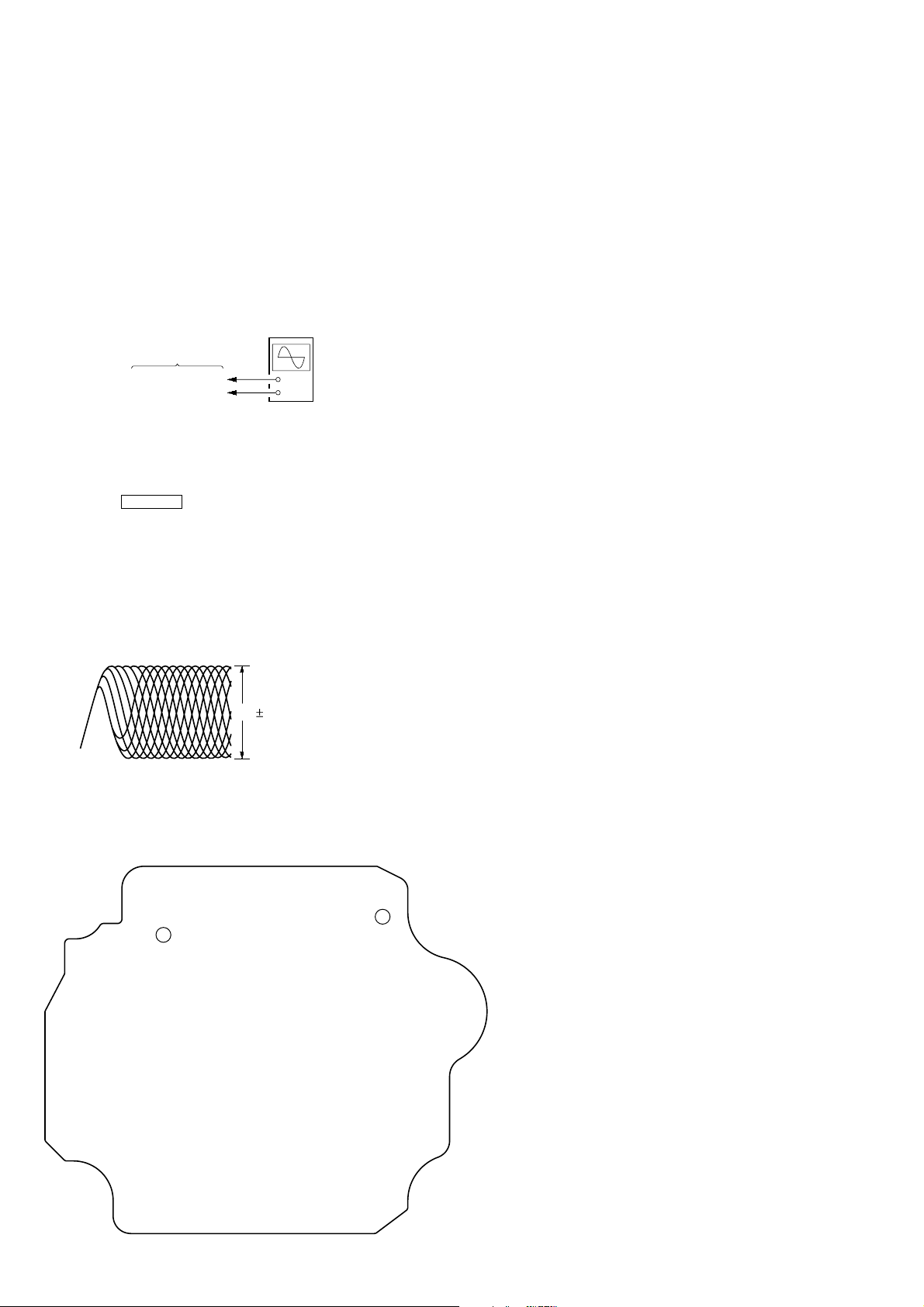
FOCUS BIAS CHECK
oscilloscope
(DC range)
BD board
TP012 (RFACO)
TP013 (VC)
+
–
Procedure :
1. Connect the oscilloscope to TP012 (RF A CO) and TP013 (VC)
on the BD board.
2. Insert the disc (YEDS-18). (Part No. : 3-702-101-01)
3. Press the CD N X button.
4. Confirm that the oscilloscope waveform is as shown in the
figure below. (eye pattern)
A good eye pattern means that the diamond shape (◊) in the
center of the waveform can be clearly distinguished.
• RF signal reference waveform (eye pattern)
VOLT/DIV: 0.2 V (with the 10: 1 probe in use.)
TIME/DIV: 500 ns
1.1
0.2 Vp-p
When observing the eye pattern, set the oscilloscope
for AC range and raise vertical sensitivity.
Checking Location:
– BD BOARD (Conductor Side) –
TP012
(RFACO)
14
TP013
(VC)
Page 15

SECTION 6
DIAGRAMS
6-1. BLOCK DIAGRAM – CD SERVO Section –
HCD-NE3
DETECTOR
A
B
C
D
F
E
OPTICAL PICK-UP
BLOCK
(KSM-213EDP)
LASER DIODE
PD
I-V AMP
LD
D +3.3V
AUTOMATIC
POWER
CONTROL
Q10
FILTER
CD DSP
IC101 (1/2)
A
25
B
26
C
27
D
28
F
19
E
18
LD
34
SUMMING
FOCUS
ERROR
TRACKING
ERROR AMP
APC LD
AMP
AMP
RF
AMP
AC_
SUM
FEO
TEO
EQ_
IN
32
23
21
PD
35
RFAC
33
VCA
RFACO
EQ
38
39
42
43
RFACI
ASYI
ASYO
DIGITAL
CLV
PROCESSOR
MDP
6
ASYMMETRY
CORRECTOR
93
XRST
48 50
FILI
PCO
FILO
CLTV
DIGITAL PLL
TO SERVO AUTO
SEQUENCER
CPU INTERFACE
DATA
CLOK
XLAT
6
8 9
1054749
XPCK
DEMODULATOR
SUBCODE
PROCESSOR
EXCK
SCOR
SENS
SBSO
SQSO
89 90
91 9210810095 98 97 103 104
7 27
EFM
SQCK
WFCK
XUGF
INTERNAL BUS
GFS
EMPH
64
106
32K
RAM
ERROR
CORRECTOR
D/A
DIGITAL
INTERFACE
110 86
C4M
GENERATOR
D/A
CONVERTER
SELECTOR
LRCK
BCK
PCMD
59 62 61
XTSL
CLOCK
LRCKI
BCKI
58 56 57
PCMDI
XTAO
XTAI
XTACN
AOUT1
AOUT2
72
73
88
76
81
R-CH
X171
16.9344MHz
CD
(Page 16)
A
2-AXIS
DEVICE
(TRACKING)
(FOCUS)
M101
(SPINDLE)
M102
(SLED)
CD XLT
CD CLK
CD SENS
CD DATA
MOTOR/COIL DRIVE
IC251
CH4OUTF
16
M
M
15
17
18
14
13
12
11
CH4OUTR
CH1OUTF
CH1OUTR
CH2OUTF
CH2OUTR
CH3OUTF
CH3OUTR
MOTOR
DRIVE
MOTOR
DRIVE
DRIVE
DRIVE
MUTE
COIL
COIL
20
CH4IN
CH3FIN
CH3RIN
CH1FIN
CH1RIN
CH2FIN
CH2RIN
OPIN+
24
23
22
4
5
6
7
OPOUT
27
9
10
11
12
13
14
2
CD DSP
IC101 (2/2)
SFDR
SRDR
TFDR
TRDR
FFDR
FRDR
FOCUS/TRACKING/SLED
20 22
CONVERTER
TRACKING/SLED
SERVO DSP
PWM GENERATOR
S101
(LIMIT)
FEI
TEI
A/D
FOCUS/
SSTP
7
MIRR,
DFCT, FOK
DETECTOR
SERVO
INTERFACE
SERVO AUTO
SEQUENCER
TO CPU INTERFACE
FOK
MIRR
DFCT
COUT
SCLK
SYSTEM CONTROLLER
3
1
2
112
101
CD XRST
5
CD SCOR
IC801 (1/2)
CD XTXCN
3
• R-ch is omitted due to same as L-ch.
• SIGNAL PATH
: CD PLAY
1515
Page 16

HCD-NE3
6-2. BLOCK DIAGRAM – MAIN Section –
J303
L
MD
(Page 15)
ANTENNA
A
FM 75Ω
COAXIAL
AM
R
CD
FM/AM TUNER PACK
FM ANT
TU-LCH
TU-RCH
ANT GND
AM ANT
ANT GND
TU-DI
TU-DO
TU-CL
TU-CE
TUNED
STEREO
MUTE
R-CH
STEREO
TU-MUTING
R-CH
CLK
TUNED
AUX-L
19
18
OUT-L
CD-L
21
TU-L
23
DO
DI
CE
INPUT SELECT,
ELECTRICAL VOLUME
IC302
REC-O-L
28
R-CH
POWER
AMP
IC501
J301
PHONES
+
• R-ch is omitted due to same as L-ch.
• SIGNAL PATH
: TUNER
+
–
+
–
L
R
J302
SPEAKER
IMPEDANCE
USE 6 – 16Ω
: CD PLAY
: TAPE PLAY
: REC
: AUX IN
HRPE301
(REC/PB/ERASE)
TAPE MECHANISM
DECK BLOCK
MOTOR 9V
MM
(CAPSTAN/REEL)
(DECK-A)
SOL 9V
PACK
REC
PLAY SW
FWD SW
L-CH
R-CH R-CH
ERASE
CAPSTAN/REEL
MOTOR DRIVE
Q804, 805
PLUNGER
DRIVE
Q802, 803
FL801
FLUORESCENT
INDICATOR TUBE
REMOTE CONTROL
RECEIVER
IC802
Q326 – 332
93
TA MOTOR
96
TA SOL
24
TA-SW
TA PLAY SW
91
TA END SW
92
53 – 45
79 – 56,
LCD COM0 – 3
83 – 86
RMC
29
REC/PB
SWITCH
SEG1 – 33
DO
32
DI
30
TU DO
CLK
34
TU DI
CE
35
TU CLK
TA-L
2
BIAS OSC
T301
TUNED
STEREO
TU-MUTING
36
37
33
TU CE
TU MUTE
TU TUNED
TU STEREO
BACK LIGHT ON
97
LED DRIVE
Q808
D701 – 703
(LCD BACK LIGHT)
BIAS OSC
Q344, 345
REC BIAS
SWITCH
Q346 – 348
95
94
TA BIAS
TA REC/PLAY
SYSTEM CONTROLLER
ST/BY
39
LED DRIVE
Q806
D806
(STANDBY)
CONT
13
B +10V
28
IC801 (2/2)
S801 – 813
(FRONT PANEL KEYS)
X801
32.768kHz
13 12
F DATA
(CD LID OPEN/CLOSE DETECT)
VOLUME
XT2
16 15
XT1
S820
ROTARY
ENCODER
RV801
X802
10MHz
CF2
98
CF1
99
AMP STBY
AMP MUTE
4 CD OPEN
22 VOL ENCODER
KEY0,
KEY1
25, 26
DC
DETECT
Q342, 343
D307
+
AC
DETECT
Q333, 338
18
I POWER MONITOR
MAIN POWER
TRANSFORMER
T902
D920, 921
TO
POWER AMP
+3.3V
Q801
REGULATOR
Q317
SYS +3.3V
VM +10V
SYS +3.1V
SYS +3.2V
D809
D810
REGULATOR
+3.3V
REGULATOR
Q339
VOLTAGE
DETECT
IC803
+7V
IC306
D +3.3V
M +7V
2CD ON
23I POWER DOWN
11RESET
1PWR ON
RESET SWITCH
AMP B+
AMP B–
B+ SWITCH
Q319, 320
REGULATOR
+3.9V
REGULATOR
Q312 – 314
+10V
IC305
RECT
D918, 919
RECT
D916, 917
RECT
D913, 914
RECT
D907 – 910
D923, 924D922
SUB POWER
TRANSFORMER
T901
(EXCEPT E, E51, EA, SP)
(E, E51, EA, SP)
VOLTAGE
SELECTOR
S901
(EXCEPT E, E51, EA, SP)
MAIN POWER
RELAY DRIVE
Q311, 315
RY901
(AC IN)
1616
Page 17

HCD-NE3
6-3. NOTE FOR PRINTED WIRING BOARDS AND SCHEMATIC DIAGRAMS
Note on Printed Wiring Board:
• X : parts extracted from the component side.
• Y : parts extracted from the conductor side.
f
•
• : Pattern from the side which enables seeing.
(The other layers' patterns are not indicated.)
Caution:
Pattern face side: Parts on the pattern face side seen from
(Conductor Side) the pattern face are indicated.
Parts face side: Parts on the parts face side seen from
(Component Side) the parts face are indicated.
• Indication of transistor.
: internal component.
C
Q
B
E
B
B
These are omitted.
Q
CE
Q
CE
These are omitted.
These are omitted.
Note on Schematic Diagram:
• All capacitors are in µF unless otherwise noted. pF: µµF
50 WV or less are not indicated except for electrolytics
and tantalums.
• All resistors are in Ω and 1/
specified.
f
•
• 2 : nonflammable resistor.
• 5 : fusible resistor.
• C : panel designation.
• A : B+ Line.
• B : B– Line.
•Voltages and waveforms are dc with respect to ground
•Voltages are taken with a VOM (Input impedance 10 MΩ).
•Waveforms are taken with a oscilloscope.
• Circled numbers refer to waveforms.
• Signal path.
•Abbreviation
: internal component.
Note:
The components identified by mark 0 or dotted
line with mark 0 are critical for safety.
Replace only with part
number specified.
under no-signal conditions.
– CD Board –
no mark : CD PLAY
– Other Sections –
no mark : TUNER
(): CD PLAY
〈〈 〉〉 : TAPE PLAY
{ } : REC
Voltage variations may be noted due to normal production tolerances.
Voltage variations may be noted due to normal production tolerances.
F : TUNER
J : CD PLAY
E : TAPE PLAY
j : REC
f : AUX IN
AR : Argentina model
AUS: Australian model
CND : Canadian model
E51 : Chiliean and Peruvian models
EA : Saudi Arabia model
KR : Korean model
MX : Mexican model
SP : Singapore model
TW : Taiwan model
4
Note:
Les composants identifiés par
une marque 0 sont critiques
pour la sécurité.
Ne les remplacer que par une
pièce portant le numéro
spécifié.
W or less unless otherwise
• Circuit Boards Location
CONTROL board
HP board
BACK LIGHT board
MAIN board
BD board
AMP board
POWER board
TUNER unit
1717
Page 18

HCD-NE3
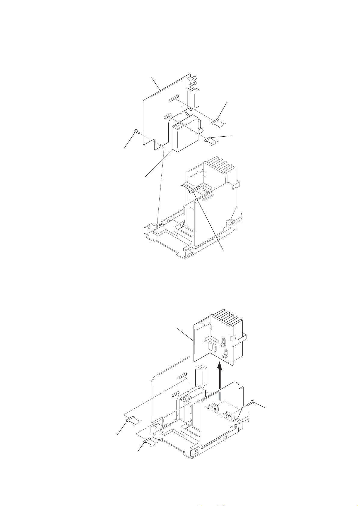
6-4. PRINTED WIRING BOARD – BD Board – • See page 17 for Circuit Boards Location. :Uses unleaded solder.
BD BOARD
C151
JW119
R202
R161
C142
R151
C143
JW123
R141
X101
R172
C172
JW124
R142
C161
C162
C171
JW125
R412
C117
R131
C131
C132
R133
C133
JW120
56
57
C174
R173
C141
R201
R143
R171
JW118
R132
R181
C182
JW103
(RFACO)
C185
JW128
JW127
TP012
C183
C201
R121
C124
C184
C123
JW114
C122
C125
IC101
C194
C181
R182
C186
JW126
JR110
C202
C203
JR104
R162
R406
2829
8584
C210
JR108
C163
R204
R407
R408
C211
R111
JW115
R113
C115
C164
JR103
C212
R409
C195
JW132
JW131
JW134
R410
C170
R12
R112
C112
C204
JW133
JR101
R114
112
JR102
JR109
C111
1
C160
C259
JR107
JW116
R252
C258
C17
C113
C114
JW117
R251
C251
C252
C257
R11
C18
JR106
14
C16
1
7
8
JW113
Q10
E
CN101
JW106
JW105
JW104
IC251
M102
(SLED)
M
R13
C116
R10
JR105
16
15
C15
2
1
28
22
21
15
JW112
JW111
JW110
JW108
JW107
C10
C14
JW109
(LIMIT)
S101
C11
JR111
TP013
(VC)
JW101
JW102
OPTICAL
PICK-UP
BLOCK
(KSM-213EDP)
M101
(SPINDLE)
M
1-861-620-
12
(12)
R411
CN201
A
MAIN BOARD
CN305
C213
(Page 20)
1818
Page 19

6-5. SCHEMATIC DIAGRAM – BD Board – • See page 28 for IC Block Diagrams. • See page 28 for Waveforms.
CN201
(Page 21)
17P
XTACN
AGND
DOUT
AVDD
LOUT
AGND
ROUT
DGND
DVDD
XRST
DATA
XLT
CLK
SENS
SCOR
MGND(7V)
M+7V
XTACN
TP29
DOUT
TP31
R161
100
TP32
R201
LOUT
TP33
AGND
TP30
ROUT
TP34
DGND
TP35
TP36
TP37
TP38
TP41
TP42
TP44
R204
DVDD
XRST
DATA
XLT
TP39
CLK
TP40
SENS
SCOR
MGND(7V)
TP43
M+7V
100
R411
C258
0.1
AVDD
C203
C202
C213
22p
R412 R162
0
JR110
0.1
100
100
100
100
100
C163
R406
R407
R408
R409
R410
C211
220p
C212
22p
100 47k
C210
0.1
0
JR104
0
JR103
C164
0.1
C160
0
0.1
JR102
C195
0.1
TRDR
TFDR
C194
0.1
RMUT
LMUT
XTSL
IOVSS0
XTACN
SQSO
SQCK
SBSO
EXCK
XRST
SYSM
DATA
VSS
XLAT
CLOK
VDD
SENS
SCLK
ATSK
WFCK
XUGF
XPCK
GFS
C2PO
SCOR
VDD
C4M
WDCK
COUT
MIRR
C259
0.1
FRDR
FFDR
F-
F+T+T+T-T-
IOVDD0
DFCT
C186 C185
470p 470p
100
C184 C183
220
10V
R182
AOUT2
AVDD2
VSS
FOK
R252C251
22k6800p
VREFR
LOCK
AVSS2
MDP
0.1
100
220
10V
R181
XVDD
VREFL
AVSS1
AOUT1
AVDD1
TFDR
SRDR
SFDR
IOVSS1
SSTP
TFDR
SRDR
SFDR
TP016
SSTP
R251
10k
C162
220
0.1
10V
C174R173
0.10
C171
22p
X101
27p
16.9344MHz
R172
1M
C172
R171
470
XTAI
XTAO
XVSS
IOVSS2
CD DSP
IC101
CXD3058AR
IOVDD1
FRDR
FFDR
TRDR
FRDR
FFDR
TRDR
C115
0.1
TES1
AVDD0
TEST
AVSS0
C201
C182 C181
220
0.1 0.1
10V
C161
0.1
VSS
BCK
VDD
DOUT
EMPH
PCMD
EMPHI
IOVDD2
A
VC
FEO
TEO
F
E
FEI
TEI
E
F
JPO003
JR107
0
C112C113
470p3300p
ABBCC
JPO002
HCD-NE3
C151
220
10V
C143
PCMDI
LRCK
BCKI
LRCKI
DDCR
AVSS5
DDVRSEN
DDVROUT
AVDD5
PCO
FILI
FILO
CLTV
AVSS3
VCTL
VPCO
ASYO
ASYI
BIAS
AVDD3
RFACI
RFACO
AVSS4
RFC
PD
LD
EQ_IN
AC_SUM
PDSENS
RFDCO
AVDD4
D
C
B
D
R111R113
1k1k
C111C114 R114 R112
3300p470p 15k 15k
C122
JR109
0
C116
C10C14
220
100.1
10V
PD
0.1
R133 C133
R132
180k 0.01
10k
1M 100p
R131 C131
TP012
0.1
R151
0
R202
0
C141R142R141
0.11k4.7k
JPO001
RFACO
R143
3.3k
C132
R121
C123
C125
0.1
C142
1500p
C117
0.1
TP46
C16
1
Q10
2SB1690K
AUTOMATIC
POWER CONTROL
C15
0.1
E
D
A
F
JR106
PD
F+
F-
IOP1
R13
1
TP45
IOP2
R10
3.3
CN101
VC
TP013
TOP1
TP27
E
TP014
D
TP17
A
TP18
B
TP19
TP20
TP015
0
TP28
TP21
TP22
TP23
TP24
TP25
TP26
0
C
JR108
F
LD
AGND
PD
F+
T+
T-
F-
16P
VC
VCC
E
D
A
B
C
F
AGND
LD
VR
PD
F+
T+
T-
F-
C17
0.47
220
10V
R12
C124
100k
330p
15k
0.1
JR111
R11
0
C18
1000p
JR105
0
0
C11
10
MOTOR/COIL
DRIVE
IC251
BA5947FM
S101
(LIMIT)
C252
0.1
SRDR
SFDR
JR101
JPO004
C257
0.1
0
C170
220
16V
The components identified by mark 0 or dotted
line with mark 0 are critical for safety.
Replace only with part number specified.
M101
(SPINDLE)
M102
(SLED)
Les composants identifiés par une marque 0 sont
critiques pour la sécurité. Ne les remplacer que
par une pièce portant le numéro spécifié.
1919
Page 20

HCD-NE3
6-6. PRINTED WIRING BOARDS – MAIN Section – • See page 17 for Circuit Boards Location. :Uses unleaded solder.
• Semiconductor
Location
Ref. No. Location
D301 K-14
D302 B-13
D303 G-8
D304 I-9
D305 C-11
D306 C-10
D307 K-13
D308 M-10
D310 L-10
D317 K-12
D318 B-10
D321 E-5
D322 D-5
IC302 C-12
IC305 K-6
IC306 K-7
Q311 M-11
Q312 L-10
Q313 L-10
Q314 L-9
Q315 K-13
Q317 F-8
Q319 G-7
Q320 F-7
Q326 C-14
Q327 C-13
Q328 B-14
Q329 B-13
Q330 B-13
Q331 B-14
Q332 B-15
Q333 K-12
Q338 K-14
Q339 I-9
Q342 F-10
Q343 E-9
Q344 H-13
Q345 I-13
Q346 E-12
Q347 G-12
Q348 G-12
1 2 3 4 5 6 7 8 9 10 11 12 13 14 15 16
JW307
C134
JW314
1
JW318
C346
C135
C310
D
C333
AMP BOARD
CN502
JW308
C234
R128
R132
CNB301
C309
R305
C315
C317
C311
R304
C235
1
C218
R228
R231
C118
R131
JW321
R317
Q319
JW377
BD BOARD
A
JW302
JW309
C352
C353
R370
R373
CN201
JW383
C319
C318
C316
CN305
C232
C322
C132
9
R372
CNB308
R371
D322
D321
R359
JW315
JW316
A
B
C
D
J303
L
MD
R
C
HP BOARD
CNB501
(Page 22)
E
L
F
J302
SPEAKER
IMPEDANCE
USE 8 – 16Ω
G
R
H
(CHASSIS)
+
–
–
+
MAIN BOARD
C226
R237
R236
C370
C227
C127
R137
C126
C119
C221
C121
C219
L101
JW310
JW311
L201
R136
JW120
FB317
C323
C308
3
CN309
1
FB301
JW301
C321
JW312
JW304
JW313
I
POWER BOARD
E
CN902
(Page 26)
CONTROL BOARD
F
CNB303
(Page 24)(Page 22)(Page 18)
CN303
JW324
R232
C233
JW325
JW326
JW378
JW379
CNB307
R224
JW338
JW322
JW327
JW339
C329
JW380
JW381
R243
C133
R143
JW320
R124
C332
C331
E
R348
Q320
E
16
JW319
8
JW340
D303
JW328
E
JW329
Q317
R318
JW382
FB302
C330
C115
C215
JW331
R332
JW369
C305
JW332
E
JW341
D304
Q343
JW355
Q339
R352
R223
JW333
JW323
JW360
JW361
JW362
JW363
E
C345
C213
JW334
E
Q342
JW357
JW358
C335
C214
JW335
JW370
C351
R358
C302
R123
C114
JW371
R301
D318
JW336
JW354
JW359
JW337
D306
R220
R125
C301
C113
R222
R121
R225
R303
R302
R120
JW356
R320
C108
JW342
C208
D305
IC302
JW343
C136
CN302
R221
R118
C116
C216
JW366
JW367
JW368
R122
C320
C207
C206
R119
R126
JW364
JW365
R207
C117
JW353
R219
C236
R353
C328
C358
R360
C357
C204
R206 R106
R205
R105
C203 C103
114
2815
C210
R211
R217
R117
R116
R218
C217
R226
JW352
R368
R363
R361
R204
R212
R216
E
R213
Q347
R209
R109
Q348
C362
C104
C356
Q346
R107
R366
R365
R202
R103
R203
R214
R215
C212
C106
E
C202
JW344
C211
E
R104
C110
R367
JW384
C107
Q344
Q345
C355
R113
C361
C109
R111
R112
C111
C112
S
GDSGDSG
1
C102
R102
Q327
E
JW346
C209
JW349
R115
R114
C354
C360
R364
R362
E
E
D302
C312
Q330Q329 Q328
CN301
JW345
JW348
R208
R108
JW351
R100
R319
D
C201
Q326
C101
R101
Q331
T301
E
R200
C313
7
E
JW350
R201
C314
654
123
Q332
JW347
E
1
7
B
CONTROL
BOARD
CNB302
(Page 24)
HRPE301
(REC/PB/ERASE)
L-CH
R-CH
ERASE
J
1
CN307 CN306
C307
K
1133
IC305
133
C306
IC306
1-861-729-
11
(11)
REG BOARD
L
M
C324
Q314
R324
R325
Q313
JW372
C326
R326
Q312
Q311
C350
C336
D317
R321
R315
E
Q333
E
Q315
R350
JW375
JW376
R351
R336
D307
D301
Q338
E
1-861-724-11(11)
R327
R349
R323
D310
R322
EEE
D308
JW373
E
N
2020
Page 21

6-7. SCHEMATIC DIAGRAM – MAIN Section – • See page 28 for IC Block Diagram. • See page 28 for Waveforms.
R225 C232
0.22
50V
OUT-L
TRE-R
470
6.3V
KTA1266-GR
-AT
KRC102M-AT
R125
R126 C136
R226 C236
0.47
50V
68k
R122
OUT-R
BASS-L
VDD
CONT
15k
R302
MTZJ-T-77
Q327
KTA1504
R366
22k
Q348
22k 4.7 50V
C132
22k
4.7 50V
22k 10 50V
22k 10 50V
R223R123
2.2k2.2k
C214C213C114C113
0.47
0.22
50V
50V
R222
68k
BASS-R
INPUT SELECT,
ELECTRICAL
VOLUME
VEE
IC302
BD3881FV
D318R301
1SS133T-7747k
D305C302
C301
10p
-4.3C
C313
100
16V
R320
4.7k
Q331
KRA303
-RTK
R368
10k
C362C361
10
50V
TU LCH
TU RCH
C115
4.7
50V
C215
4.7
50V
R352
470
2SC2001TP
R360 R361
5.6 5.6
R143C133
8.2k0.047
R124
15k
R224
15k
R243C233
8.2k0.047
R231 R228 R128R131
1.2k 1.2k 1.2k1.2k
C218
0.033
D317
1SS133T-77
JW323
10UH
Q338
KRC402-RTK
D301
1SS133T-77
Q344
-LK
Q344,345
BIAS OSC
C305
470
6.3V
C355
0.015
L-CH
R-CH
ERASE
(Page 25)
MD
HRPE301
(REC/PB/ERASE)
R
L
(CHASSIS)
CN302
19P
TU-RCH
TU GND
TU-LCH
TU 10V
TA 10V
TA GND
TA BIAS
REC/PB
F DATA
A-MUTE
P-CONT
AMP-STBY
AMP-MUTE
I POWER MONITOR
AC-DET
3.3V(MAIN)
GND
GND
3.9V(SUB)
R136
10k
C117
220p
4.7k
J303
2P
C370
CN301
7P
470p
C126
R137
C127
220p
4.7k
470p
C226
R237
C227
R236
10k
0.1
TU RCH
TU LCH
TU 10V
TA 10V
TA GND
AC-DET
JW120
FB317
470p
470p
C109
C209
0.1
15k
15k
R108
R208
C101
68p
R101
12k
C314
0.01
FB302
0.0012
C217
0.0012
C216 C116
C111
C112
C212
C211
0.0033
0.0047
0.0047
R215
3.3k
470
R113
1800p
C102
T301
BIAS OSC
R114
R112
33k
R111
2.2k
C110
RECO-L
NF-L
C103
100p
R203
470
R106
5.6k
39k
1800p
R104
47
R202
C202
Q330
2SK2158
-T2B
Q329
2SK2158
-T2B
Q328
2SK2158-T2B
R115
3.3k
R109
2.2k
R209
2.2k
R103
470
39k
R102
C201
68p
R201
12k
R200R100
180180
0.0033
2.2k
RECO-R
NF-R
C106
0.022
R205
Q326-332
C312
220p
R217
8.2k
8.2k
R216
R116
TU-L
TU-R
PB0-R
PBO-L
390k
C107
C206
R107
0.022
150k
R206
5.6k
R207
150k
D302
1SS133T
-77
2SD1387-34
R364
6.8k
2.2k
R117
6.8k
R218
CD-R
VOLI-L
50V
2.2
Q346 Q347
-TP
C360
10
50V
560
560
470
R213
R214
33k
R212
180p
2.2k
R211
180p
C210
NF-L
NF-R
TA-L
TA-R
C203
100p
R105
390k
R204
47
C204C104
100
100
10V
10V
REC/PB SWITCH
S
S
R319
1M
S
Q346-348
REC BIAS
SWITCH
C354
2.2
50V
470p 470p
1.8k
1.8k
2.2k
2.2k
R219
R119
R221
R121
10k
10k
6.8k
R220
R120
R118
CD-L
AUX-L
AUX-R
VOLI-R
GND
TRE-L
50V
2.2
C207
C108
C208
0.0033
0.0033
R303
10k
Q332
KRA303
-RTK
Q326
KTA1504
R367
2.2k
R365
2.2k
47
16V
C119
0.01
C219
0.01
C121
0.1
C221
L201
0.1
L101
C235
10 50V
R132
R232
1k
C234
0.0022
R358
Q342
2SC1623-T1
-L5L6
R351
10k
C336 C346
22
50V
C356
0.0068
R362
18k
Q345
2SC2001TP-LK
1k
C118
C134
0.033
0.0022
D306
MTZJ-T-77
-4.3C
56k
Q343
2SC1623-T1
-L5L6
Q342,343
DC DETECT
Q311,315
MAIN POWER
RELAY DRIVE
R336
4.7k
Q333,338
AC DETECT
Q333
KRC402-RTK
R350
10k
0.0068
C358
0.018
C357
R363
18k
D303
MTZJ-T-77-3.9B
KTC3205Y
REGULATOR
R318
470
10V
C330
100
+3.3V
C135
10
50V
R370
10k
R371
10k
C352
2200
R359
1.5k
1000
16V
C351
100
25V
D322
1SS133T
-77
D307
1SS133T
-77
R321
100k
R315
1k
Q315
KRC402-RTK
Q317
10V
2200
C332
0.01
C331
M+7V
REG07-OUT
KTA1273Y
KRC402
REG07-IN
C324
220
16V
Q319
-AT
R348
1k
Q320
-RTK
R323 C326 R325
R322
1.5k
B+ SWITCH
35V
R372
82k
C333C309
220
50V
D321
1SS133T
-77
R373
10k
D310
MTZJ-T-77
-4.3C
Q312-314
+3.9V
REGULATOR
1k 0.0022 100k
R317
Q339
47k
KTC3203Y
CD ON
+3.3V
REGULATOR
D304
C345
MTZJ-T-77
10
-3.9B
50V
Q319,320
1SS133T-77
KTA1271Y-ATKTA1271Y-AT
KTC3203YKTC3203Y
D308
Q314Q311
R324
2.2k
Q313Q312
R326R327R349
100k10k56k
R332
C335
0.01
TA GND
1k
2200
16V
16V
470
C328
REG07-GND
HCD-NE3
J302
4P
L
SPEAKER
IMPEDANCE
USE 8-16
R
LP221
(CHASSIS)
SP OUT(R)
GND
SP OUT(L)
CN309
3P
CNB308
9P
R
AGND
L
AMP-MUTE
AMP-STBY
PROTECT
-B
GND
+B
CNB307
REG07-OUT
REG07-GND
REG07-IN
C323
2200
25V
AC-DET
M+7V
C318
CD ON
100p
C317
100p
C319
100p
C311
100p
C316
100p
C315
100p
FB301
C308
0.1
SCOR
SENS
CLOK
XLT
DATA
XRST
XTACN
C310
0.1
C322
0.001
C321
0.001
C329
1000
6.3V
R353
10
0.01
C320
TU 10V
TA 10V
6P
C353
2200
35V
SCOR
SENS
CLOK
XLT
DATA
XRST
XTACN
R305
100
R304
1k
M+7V
MGND(7V)
SCOR
SENS
CLK
XLT
DATA
XRST
DVDD
DGND
ROUT
AGND
LOUT
AVDD
DOUT
AGND
XTACN
SCOR
SENS
CLOK
XLT
DATA
XRST
XTACN
CD ON
(Page 23)
(Page 23)
+7V REGULATOR
CN306
3P
+10V REGULATOR
CN307
3P
-B
GND
+B
14V
SUB +B
PROTECT
RELAY ON
AC-DET
CNB301
8P
CN305
17P
CN303
8P
IC306
BA07T
IO
G
IC305
TA7810S
IO
G
(Page 27)
(Page 19)
(Page 25)
C306
0.1
C307
0.1
The components identified by mark 0 or dotted
line with mark 0 are critical for safety.
Replace only with part number specified.
Les composants identifiés par une marque 0 sont
critiques pour la sécurité. Ne les remplacer que
par une pièce portant le numéro spécifié.
2121
Page 22

HCD-NE3
6-8. PRINTED WIRING BOARDS – AMP Section – • See page 17 for Circuit Boards Location. :Uses unleaded solder.
MAIN BOARD
D
CNB308
AMP BOARD
(Page 20)
HP BOARD
MAIN BOARD
C
CN309
(Page 20)
CN501
R517
R519
JW509
R518
R520
JW508
9
14
C512
R516
C511
C514
C513
C509
JW510
CN502
R515
C510
1
J301
PHONES
C521
C520
CNB501
1
7
1-861-728-
11
(11)
(CHASSIS)
2
10
14
IC501
JW504
JW503
1
5
C505
C501
15
EP903
R509
JW501
R504
JW506
R507
JW511
R503
JW512
R508
C507
C516
C506
JW502
C503
JW505
JW507
R511
R506
R501
JW513
R512
R505
R502
R514
1-861-726-
11
(11)
2222
Page 23

6-9. SCHEMATIC DIAGRAM – AMP Section –
CN502
9P
+B
GND
-B
PROTECT
AMP-STBY
AMP-MUTE
(Page 21)
L
AGND
R
R501
HCD-NE3
R515
10k
R514
10k
R507
C506
47
25V
R506
R508
1k
R502
47k
C503
25V
R503
680
47
C507
0.1
R505
47k
1k
680
R512
33k
C516
100
16V
R511
33k
C509 C510
220
220
35V
35V
2.2
C512
C511 C513
R517
56k
R518
47k
R516
2.2
C514
1
11
R519
330
R520
330
1
EP903
CN501
SP OUT(R)
HP OUT(R)
HP OUT(L)
SP OUT(L)
4P
R509C505
R504C501
47k100p
47k100p
POWER AMP
IC501
LM1876TF
(CHASSIS GND)
(Page 21)
CNB501
7P
SP OUT(R)
HP OUT(R)
HP OUT(L)
SP OUT(L)
SP OUT(R)
GND
SP OUT(L)
J301
PHONES
C521C520
10000p10000p
The components identified by mark 0 or dotted
line with mark 0 are critical for safety.
Replace only with part number specified.
Les composants identifiés par une marque 0 sont
critiques pour la sécurité. Ne les remplacer que
par une pièce portant le numéro spécifié.
2323
Page 24

HCD-NE3
6-10. PRINTED WIRING BOARDS – PANEL Section – • See page 17 for Circuit Boards Location. :Uses unleaded solder.
• Semiconductor
Location
Ref. No. Location
D701 C-1
D702 B-1
D703 B-1
D801 H-9
D806 G-13
D807 G-3
D808 I-3
D809 F-12
D810 F-11
D811 F-11
D812 F-11
IC801 D-7
IC802 D-13
IC803 H-4
Q801 G-4
Q802 H-10
Q803 H-10
Q804 H-11
Q805 H-10
Q806 H-13
Q808 C-4
1 2 3 4 5 6 7 8 9 10 11 12 13 14 15
A
B
C
D
BACK LIGHT
BOARD
1
R712
R711
2
D703
R710
R709
D702
R708
R707
D701
1-861-730-11(11)
CD LID OPEN/CLOSE
CNB807
D701 – 703
LCD BACK
LIGHT
S820
DETECT
E
F
G
H
I
J
CONTROL BOARD
Q808
CNB806
1
2
R704
CNB804
R801
1
2
R832
R882
S813
DSGX
Q801
R806
R892
D807
C826
IC803
C816
3
1
D808
JW815
R703
BASS/TREBLE
R863
JW871
C823
R894
R893
C825
R878
ROTALY ENCODER
3
S812
R816
RV801
VOLUME
C829
C824
C828
JW807
1
R879
C832
JW804
JW801
JW805
JW802
JW808
JW809
JW810
JW811
JW812
JW813
R895
JW803
JW806
S811
DISPLAY
JW814
CNB801
37
R835
R834
X801
C805
C813
JW850
R870
R874
R869
JW845
JW816
R871
TAPE MECHANISM
DECK BLOCK
SUPPLIED WITH THE
ASSEMBLED BLOCK
R839
X802
R862
C834
JW817
R833
R838
100
JW868
1
C830
R702
C801
C802
R705
(EXCEPT US, CND)
C812
JW849
JW819
JW870
C804
JW818
R706
C827
JW820
R890
R891
81
R809
R813
R812
R876
R701
(US, CND)
(EXCEPT AEP, UK)
JW821
S804
TUNER
BAND
JW822
80
IC801
30 31
R815
R811
R814
R875
(EXCEPT SP, TW, KR, AUS)
JW825
R855
JW823
S805
CD SYNCHRO
LCD801
LIQUID CRYSTAL DISPLAY
51
50
R840
R810
R818
JW828
R856
JW826
R861
S810
TUNE +
JW829
C803
R827
R826
R825
R824
R822
JW832
R831
C811
JW830
JW824
S806
REC PAUSE/START
JW863
R837
R823
JW833
CNB302
JR107
JW859
JW861
JW869
C815
S808
JW846
JW844
JW867
JW865
JR106
JR109
R881
JR101
JW848
C809
R805
R804
R803
IC802
C810
CNB303
JR105
D806
(STANDBY)
Q806
S801 – 813
C831
13
R887
S801
1-861-725-11(11)
B
MAIN
BOARD
CN302
(Page 20)
FM/AM
TUNER
PACK
SUPPLIED
WITH THE
ASSEMBLED
BLOCK
F
MAIN
BOARD
CN303
(Page 20)
FM 75Ω
(COAXIAL)
AM
ANTENNA
JR102
JR103
837
JW
R836
R898
R897
JW835
JW834
R860
D801
JW831
R854
S803
CD
R857
R820
JW836
Q802
JR104
JW827
E
R884
R883
JW855
JW856
JW838
S809
TUNE –
Q805
Q803
S807
PLAY MODE
JW839
R859
JW840
JW864
Q804
E
JW842
JW847
S802
TAPE
C814
JW857
R885
D811
JW858
L801
R886
R853
D812
CNB802
JW860
D810
JW843
JW866
D809
JW862
R858
JW853
R851
R852
2424
Page 25

6-11. SCHEMATIC DIAGRAM – PANEL Section – • See page 28 for Waveforms. • See page 30 for IC Pin Function Description.
SEG6
SEG5
SEG4
SEG3
SEG2
SEG1
SEG7
SEG6
SEG5
SEG4
SEG3
SEG2
SEG1
R832
47k
ANTENNA
FM 75Ω
COAXIAL
AM
FM/AM
TUNER PACK
SUPPLIED WITH
THE ASSEMBLED
BLOCK
(Page 21)
TAPE MECHANISM
DECK BLOCK
SUPPLIED WITH
THE ASSEMBLED
BLOCK
CNB802
CNB303
CNB801
11P
8P
7P
PLAY SW
REC
PACK
MOTOR 9V
SOL9V
COM GND
END SW
MUTE
TU-RCH
TU GND
TU-LCH
STEREO
TUNED
TU 10V
TU-CE
TU-DI
TU-DO
TU-CL
CD ON
XTACN
XRST
DATA
XLT
CLOK
SENS
SCOR
TU RCH
TU GND
TU LCH
TU 10V
R833R851R858
47k3.3k3.3k
BIAS3
25
S808
0.1
33
37
36
35
32
30
34
2
3
5
6
9
8
7
27
S809
C815
TUNE -
R860
330
S810
TUNE +
R861
470
S811
DISPLAY
R862
680
S812
BASS/TREBLE
R863
1k
S813
DSGX
R871
10k
S801
S802
TAPE
S803
S804
TUNER
BAND
S805
CD SYNCHRO
S806
REC PAUSE/START
S807
PLAY MODE
26
R852R859
220220
R853
330
CD
R854
470
R855
680
R856
1k
R857
1.5k
C813C832
0.10.01
C804
0.01
R869
10k
92
91
R834
47k
COM0
COM1
COM2
COM3
R835
47k
100
91
R838
92
93
R839
94
95
96
97
98
99
100
24
R870 R874 C834
10k 10k 0.1
D801
1SS133T-77
C811
22
16V
100
Q802,803
PLUNGER
96
DRIVE
LCD BIAS2
LCD BIAS1
LCD COM0
LCD COM1
LCD COM2
LCD COM3
NC
NC
VSS3
VDD3
TA PLAY SW
TA END SW
TA MOTOR
TA REC/PLAY
TA BIAS
TA SOL
BACK LIGHT ON
AMP STBY
AMP MUTE
AU MUTE
PWR ON
Q803
KRC402-RTK
R884
SEG1
2
1
Q802
KTA1271Y-AT
1k
SEG1
CD ON
SEG2
3
SEG3
SEG2
CD XTXCN
100
R801
4
SEG4
SEG3
CD OPEN
5
SEG4
CD XRST
SEG5
100
R803
6
93
SEG6
SEG5
CD DATA
100
R804
7
SEG6
CD SENS
SEG8
SEG7
SEG7
CD CLK
100
R805
8
9
KTA1271Y-AT
R883
47k
KRC402-RTK
SEG9
SEG8
CD XLT
1k
R806
11
(EXCEPT US,CND)
Q804
Q805
TA GND
HCD-NE3
LCD801
LIQUID CRYSTAL DISPLAY
3
COM0
COM1
COM2
COM
SEG33
SEG32
SEG31
SEG30
SEG29
SEG28
SEG27
SEG26
SEG25
SEG24
SEG23
SEG22
SEG21
SEG20
SEG19
SEG18
SEG17
SEG16
SEG15
SEG14
SEG13
SEG12
SEG11
SEG10
SEG9
SEG8
SEG7
CNB806
R882
100k
R881
C809
0.01
D811R890
TU RCH
TU GND
TU LCH
TU 10V
TA 10V
TA GND
95
94
28
100
1
98
99
18
AC DET
4
100
2P
BLT-
BLT+
C814
0.1
OPEN/CLOSE
GND
D810
1SS133T-77
10µH
L801
D809
1SS133T-77
R894
22k
Q801
KTC3875
RESET
SWITCH
SEG8
SEG23
SEG22
SEG21
SEG20
SEG19
SEG18
SEG17
SEG16
SEG15
SEG14
SEG13
SEG12
SEG11
SEG10
SEG9
NC
0.1
C830
C801
SEG10
RESET
32.768KHz
X801
SEG12
SEG11
XT2
XT1
22p
C802
20p
R706
3.3k
R705
27k
R886
1k
SEG14
SEG13
SYSTEM CONTROLLER
IC801
LC877456C-53K5-E
CF1
VSS1
390k
R702
Q804,805
CAPSTAN/REEL
MOTOR DRIVE
C827
R885
47k
SEG15
CF2
C812
0.01
10
16V
R701
33k
SEG17
SEG16
ER MONITOR
VDD1
I POW
X802
10MHz
220k
R809
18
(US,CND)
(EXCEPT AEP,UK)
SEG18
NC
TA 10V
SEG19
NC
100
R812
SEG21
SEG20
AREA
VOL ENCODER
47k
22k
R814
R813
22
23
(EXCEPT SP,TW,KR,AUS)
R875
*
R876
*
SEG23
SEG22
N
ER DOW
TA-SW
I POW
100
R815
24
R887
470
SLR-342VRT32
(STANDBY)
4.7k
KRC402-RTK
C803
SEG25
SEG24
VSS2
VDD2
SEG24
KEY0
KEY1
CD SCOR
100
100
100
R818
R810
R811
26
25
27
28
R879
10k
C828
0.01
* R875
0
(AEP,UK)
1k
(E,E51,EA,MX,AR)
2.2k
(US,CND)
*0R876
(SP,TW,KR,AUS)
(US,CND,E,E51,EA,MX,AR)
D806
Q806
LED DRIVE
0.01
SEG27
SEG26
SEG27
SEG26
SEG25
TU STEREO
F DATA
TU DI
RMC
100
56k
R822
R820
30
29
ROTALY ENCODER
VOLUME
39
SEG28
SEG29
SEG30
SEG31
SEG32
SEG33
CD LED
TU LED
TA LED
MD LED
TU TUNED
TU CLK
TU MUTE
ST/BY
TU CE
TU DO
KTC3875
LED DRIVE
NC
NC
NC
Q808
R895
10k
R816RV801
22k
R878
10k
C829 C831
0.01 220p
C824
47
6.3V
22
C816
0.1
AC DET
VOLTAGE DETECT
M62703SL-TP
R704
100k
SEG28
SEG29
SEG30
SEG31
SEG32
SEG33
R827
100
R826
100
R825
100
R831
100
R824
100
R823
100
R840
47k
29
D808 R891
1SS133T-77 4.7k
IC803
OGI
R703
10k
97
C823
470
6.3V
C805
0.01
39
R837
4.7k
37
36
R836
35
4.7k
34
R898
33
100k
32
R897
100k
REMOTE CONTROL RECEIVER
IC802
RPM7240-H9
RV
G
C810
22
6.3V
D812
1SS133T-77
C826
R892
0.1
47k
C825 D807 R893
0.1 1SS133T-77 47k
1SS133T-77220
COM0
COM1
COM2
COM3
SEG33
SEG32
SEG31
SEG30
SEG29
SEG28
SEG27
SEG26
SEG25
SEG24
SEG23
SEG22
SEG21
SEG20
SEG19
SEG18
SEG17
SEG16
SEG15
SEG14
SEG13
SEG12
SEG11
SEG10
SEG9
TU-RCH
TU GND
TU-LCH
TU 10V
TA 10V
TA GND
TA BIAS
REC/PB
F DATA
AU-MUTE
POWER ON
AMP-STBY
AMP-MUTE
I POWER MONITOR
AC-DET
3.3V(MAIN)
GND
GND
3.9V(SUB)
CNB804
2P
11
23
CNB807
D701-703
(LCD BACK LIGHT)
D701
SELS6B14CS-TP5
2P
CNB302
D702
SELS6B14CS-TP5
D703
SELS6B14CS-TP5
19P
R707
120
R708
120
R709
120
R710
120
R711
120
R712
120
(Page 21)
S820
CD LID
OPEN/CLOSE
DETECT
2525
Page 26

HCD-NE3
6-12. PRINTED WIRING BOARD – POWER Board – • See page 17 for Circuit Boards Location. :Uses unleaded solder.
• Semiconductor
Location
Ref. No. Location
D906 F-4
D907 E-5
D908 E-5
D909 E-4
D910 E-4
D911 D-4
D912 E-5
D913 D-5
D914 E-5
D916 E-5
D917 D-5
D918 E-6
D919 D-6
D920 E-5
D921 E-5
D922 F-5
D923 E-4
D924 F-5
A
B
1 2 3 4 5 6
POWER BOARD
(EXCEPT E, E51, EA, SP)
JW906
T902
MAIN POWER
TRANSFORMER
JW909
JW907
(EXCEPT E, E51, EA, SP)
VOLTAGE
-2
220 – 240V 110 – 120V (E, E51, SP)
220 – 240V 120 – 127V (EA)
-1
SELECTOR
S901
(E, E51, EA, SP)
∗
NOT REPLACEABLE:
∗
BUILT IN TRANSFORMER
JW904
C
D
E
JW908
C908
D919
D918
C907
1-861-727-
11
(11)
R905
C914
D911
C915
JW903
C902
D914
D910
D913
D909
C910
C912
D924
D922
C909
JW910
JW911
R902
D921
C911
CN902
C901
D907
D908
D917
C906
R901
C905
D916
D920
D912
18
T901
SUB POWER
TRANSFORMER
JW901
JW912
C913
LF901
RY901
CN901
12
R903
F
(US, CND)
R910
C903
R904
D923
D906
R906
(AC IN)
2626
E
MAIN BOARD
CNB301
(Page 20)
Page 27

6-13. SCHEMATIC DIAGRAM – POWER Board –
C907
0.022
D918
1N5401M
D916
1N5401M
C905
0.022
HCD-NE3
T902
MAIN POWER
TRANSFORMER
(Page 21)
CN902
8P
-B
GND
+B
14V
SUB +B
PROTECT
RELAY ON
AC-DET
D920
1SS133T-77
D921
1SS133T-77
C910
0.022
C912
0.022
R901
47k
R902
47k
C908
0.022
D913
1N4002B
D914 D912
1N4002B 1N4002B
D919
1N5401M
D911 C909
1N4002B 0.022
R903
3.3M
(US,CND)
D917
1N5401M
C911
0.022
C906
0.022
C901C902
0.10.1
C903
D906
1SS133T-77
0.1
R910
0.15
NOT REPLACEABLE:*
BUILT IN TRANSFORMER
C913
0.01
RY901
JW907
(EXCEPT E,E51,EA,SP)
110-120V 220-240V
(E,E51,EA,SP)
-1 -2
S901
VOLTAGE SELECTOR
(E,E51,SP)
220-240V120-127V
(EA)
LF901
CN901
2P
909
JW
(EXCEPT E,E51,EA,SP)
(AC IN)
D922
RB441Q-40T-77
C914
25V
D909
1SS133T-77
D910
1SS133T-77
47
R906 R904
*
2.2k
1SS133T-77
D923
R905
2.2k
D924
1SS133T-77
D907
1SS133T-77
D908
1SS133T-77
*
1k
1.2k
R906
(US,CND,AEP,UK,KR)
(EXCEPT US,CND,AEP,UK,KR)
C915
0.1
T901
SUB POWER
TRANSFORMER
The components identified by mark 0 or dotted
line with mark 0 are critical for safety.
Replace only with part number specified.
Les composants identifiés par une marque 0 sont
critiques pour la sécurité. Ne les remplacer que
par une pièce portant le numéro spécifié.
2727
Page 28

HCD-NE3
• Waveforms
– BD Board –
1 IC101 w; (TEI) (CD Play mode)
Approx.
400 mVp-p
2 IC101 ws (FEI) (CD Play mode)
Approx.
200 mVp-p
3 IC101 ek (RFACO) (CD Play mode)
0.6 Vp-p
4 IC101 us (XTAO) (CD Play mode)
– MAIN Board –
qa T301 4 (REC mode)
13
µ
s
qs Q344 (Collector) (REC mode)
13
µ
s
150 Vp-p
15 Vp-p
– CONTROL Board –
wa IC801 qd (XT2)
30.5
µ
s
ws IC801 qh (CF2)
100 ns
3 Vp-p
2.9 Vp-p
• IC Block Diagrams
– BD Board –
IC101 CXD3058AR
MIRR
DFCT
FOK
VSS
LOCK
MDP
SSTP
IOVSS1
SFDR
SRDR
TFDR
TRDR
FFDR
FRDR
IOVDD1
AVDD0
AVSS0
TEO
FEO
1
2
3
4
5
6
7
8
9
10
11
12
13
14
15
16
17
18
E
19
F
20
TEI
21
22
FEI
23
24
VC
MIRR
DFCT
FOK
VC
COUT
112
111
SERVO
INTERFACE
PWM
GENERATOR
SERVO
DSP
A/D
CONVERTER
TE
FE
WDCK
110
C4M
WFCK
ATCK
C2PO
XPCK
XUGF
SCOR
GFS
107
105
104
106
VDD
109
108
SCLK
103
102
101
DIGITAL
CLV
100
SENS
VDD
SEQUENCER
CORRECTOR
CLOK
SERVO
AUTO
ERROR
VSS
XLAT
CPU INTERFACE
INTERFACE
DATA
D/A
XRST
SYSM
COVERTER
D/A
32k
RAM
EXCK
89
90
919798
929394959699
88
CLOCK
GENERATOR
DIGITAL OUT
SELECTOR
87
85
86
84
RMUT
83
IOVDD0
82
AVDD2
81
LPF
LPF
80
79
78
77
76
75
74
73
72
71
70
69
68
67
66
65
64
63
62
61
60
59
AOUT2
VREFR
AVSS2
AVSS1
VREFL
AOUT1
AVDD1
XVDD
XTAI
XTAO
XVSS
IOVSS2
TES1
TEST
DOUT
IOVDD2
EMPHI
EMPH
VDD
BCK
PCMD
VSS
LRCK
LMUT
XTSL
IOVSS0
XTACN
SQSO
SQCK
SBSO
59 ns
3.4 Vp-p
EFM
44
VPCO
45
46
VCTL
DEMODULATOR
DIGITAL
PLL
48
47
49
FILI
FILO
CLTV
AVSS3
DC/DC
CONVERTER
53
52
DDVROUT
54
AVSS5
DDVRSEN
55
56
DDCR
51
50
PCO
AVDD5
BCKI
58
LRCKI
57
PCMDI
25
A
26
B
27
C
28
D
29
30
AVDD4
SUM
31
RFDCO
32
PDSENS
AC_SUM
ATT
33
34LD35
EQ_IN
APC
SUB CODE
PROCESSOR
ASYNMMETRY
EQ
AMP
36
38
37
PD
RFC
AVSS4
RFACO
CORRECTOR
39
40
RFACI
41
AVDD3
42
BIAS
ASYI
43
ASYO
2828
Page 29

IC251 BA5947FM
PREVCC
OPOUT
OUTVREF
28
26
27
CH4CAPA
25
24
CH4IN
23
CH3FIN
22
CH3RIN
HCD-NE3
GND
MUTE
POWVCC
CH3OUTF
CH3OUTR
CH4OUTF
CH4OUTR
20
21
18
19
16
17
15
–
+
1
2
3
OPIN+
SW
OPIN–
– MAIN Board –
IC302 BD3881FV
+
–
INTERFACE
4
CH1FIN
5
CH1RIN
INTERFACE
INTERFACE
6
CH2FIN
7
CH2RIN
MUTING
10
POWVCC
D
11
CH2OUTR
VREF
9
8
GND
VREFIN
D
D
12
CH2OUTF
D
LEVEL SHIFT
D D
13
CH1OUTR
DD
14
CH1OUTF
REC1O27REC1N
28
1
2
PB1P3PB2P
PB1N
REC2N25REC2O24INC223INC122INB221INB120INA219INA1
26
VOLUME
VOLUME
4
PB2N
5
PB2O
6
PB1O
7
VOLIN18VOLIN2
OUT117BAS116OUT215BAS2
18
BASS
TREBLE
9
GND
10
TRE1
TREBLE
11
TRE2
BASS
12
LOGIC
CONTROL
13
VDD
CONT
14
VEE
29
Page 30

HCD-NE3
• IC Pin Function Description
CONTROL BOARD IC801 LC877456C-53K5-E (SYSTEM CONTROLLER)
Pin No. Pin Name I/O Description
1
2
3 CD XTXCN O
4 CD OPEN I CD lid open/close detection switch input terminal
5 CD XRST O
6 CD DATA O Serial data output to the CD DSP
7 CD SENS I Internal status (SENSE) signal input from the CD DSP
8 CD CLK O Serial data transfer clock signal output to the CD DSP
9
10
11 RESET I
12
13
14
15 CF1 I
16 CF2 O
17 VDD1 —
18
19, 20
21
22
23
24 TA-SW
25, 26
27
28
29 RMC I
PWR ON O
CD ON O
CD XLT
NC
XT1 I Sub system clock input terminal (32.768 kHz)
XT2 O Sub system clock output terminal (32.768 kHz)
VSS1 — Ground terminal
I POWER
MONITOR
NC
AREA I Model destination setting terminal
VOL ENCODER
I POWER DOWN
KEY1, KEY0 I Front panel key input terminal (A/D input)
CD SCOR
F DATA
Power relay drive signal output terminal “H”: on
Power on/off control signal output for the CD mechanism section
Oscillation circuit control signal output to the CD DSP
“H”: auto oscillation, “L”: oscillation off
Reset signal output to the CD DSP
O
Serial data latch pulse output to the CD DSP
—
Not used
Reset signal input from the reset switch “L”: reset For several hundreds msec. after the power
supply rises, “L” is input, then it changes to “H”
Main system clock input terminal (10 MHz)
Main system clock output terminal (10 MHz)
Power supply terminal (+3.2V)
I
Power monitor input terminal
—
Not used
I Dial pulse input of the rotary encoder (for VOLUME control)
I
Power down detection signal input terminal “L”: power down, normally : “H”
I Cassette in/out detect switch signal input from the tape mechanism deck “L”: cassette in
I
Subcode sync (S0+S1) detection signal input from the CD DSP
O
Serial data output to the electrical volume
Remote control signal input from the remote control receiver
30 TU DI I Serial data input from the FM/AM tuner unit
31
32 TU DO O Serial data output to the FM/AM tuner unit
33 TU MUTE O Tuner muting on/off control signal output to the FM/AM tuner unit
34 TU CLK O serial data transfer clock signal output to the FM/AM tuner unit
35 TU CE O Chip enable signal output to the FM/AM tuner unit
36 TU TUNED I Tuning detection signal input from the FM/AM tuner unit
37 TU STEREO I FM stereo detection signal input from the FM/AM tuner unit
38
39
40
NC
NC
ST/BY O
MD LED O
—
Not used
—
Not used
LED drive signal output terminal
LED drive signal output terminal
30
Page 31

Pin No. Pin Name I/O Description
HCD-NE3
41
42
43
44
45 to 53 SEG33 to SEG25 O Segment drive signal output to the fluorescent indicator tube
54
55 VSS2 — Ground terminal
56 to 79 SEG24 to SEG1 O Segment drive signal output to the fluorescent indicator tube
80 BIAS3 I
81 LCD BIAS2 I
82 LCD BIAS1 I
83 to 86
87, 88 NC
89 VSS3 — Ground terminal
90 VDD3 —
91 TA PLAY SW I PLAY switch signal input from the tape mechanism deck
92 TA END SW I END switch signal input from the tape mechanism deck
93 TA MOTOR
94
95
96
97
98
99
TA LED O
TU LED O
CD LED O
NC
VDD2 —
LCD COM0 to
LCD COM3
TA REC/PLAY O
TA BIAS O
TA SOL O
BACK LIGHT ON
AMP STBY O
AMP MUTE
LED drive signal output terminal
LED drive signal output terminal
LED drive signal output terminal
—
Not used
Power supply terminal (+3.1V)
Power supply output for the liquid crystal display bias
Power supply output for the liquid crystal display bias
Power supply output for the liquid crystal display bias
O Common drive signal output to the liquid crystal display (D621)
—
Not used
Power supply terminal (+3.1V)
O
Capstan/reel motor on/off control signal output terminal “H”: motor on
Recording/playback selection signal output terminal “H”: playback mode, “L”: recording mode
Recording bias on/off selection signal output terminal “H”: bias on, “L”: bias off
Trigger plunger on/off control signal output terminal “H”: plunger on
O
LED drive signal output terminal for the LCD back light
Standby control signal output to the power amplifier
O Tuner muting on/off control signal output to the power amplifier
100 AU MUTE O Line muting on/off control signal output terminal Not used
31
Page 32

HCD-NE3
SECTION 7
EXPLODED VIEWS
NOTE:
• -XX and -X mean standardized parts, so they
may have some difference from the original
one.
• Color Indication of Appearance Parts
Example:
KNOB, BALANCE (WHITE) . . . (RED)
•Abbreviation
AR : Argentina model
AUS: Australian model
CND : Canadian model
↑↑
Parts Color Cabinet's Color
E51 : Chilean and Peruvian model
EA : Saudi Arabia model
KR : Korea model
7-1. PANEL SECTION
not supplied
#1
3
• Items marked “*” are not stocked since they
are seldom required for routine service. Some
delay should be anticipated when ordering
these items.
• The mechanical parts with no reference number in the exploded views are not supplied.
• Accessories are given in the last of the electrical parts list.
MX : Mexican model
SP : Singapore model
TW : Taiwan model
6
top panel assy
#8
not supplied
(REG board) (1/2)
not supplied
8
The components identified by mark
0 or dotted line with mark 0 are
critical for safety.
Replace only with part number
specified.
Les composants identifiés par une
marque 0 sont critiquens pour la
sécurité.
Ne les remplacer que par une pièce
portant le numéro spécifié.
#1
#1
#8
#8
#1
#1
#8
2
front panel assy-1
#1
#1
not supplied
(REG board) (2/2)
Ref. No. Part No. Description Remark
1 A-1055-614-A POWER BOARD, COMLETE (E, E51, SP)
1 A-1056-003-A POWER BOARD, COMLETE (AR, AUS)
1 A-1056-266-A POWER BOARD, COMLETE (MX, TW)
1 A-1056-495-A POWER BOARD, COMLETE (EA)
1 A-1056-526-A POWER BOARD, COMLETE (KR)
1 A-4750-273-A POWER BOARD, COMLETE (AEP, UK)
1 A-4751-335-A POWER BOARD, COMLETE (US, CND)
2 A-4750-277-A AMP BOARD, COMPLETE
3 A-4750-275-A MAIN BOARD, COMPLETE
4 3-703-244-00 BUSHING (2104), CORD
05 1-775-790-12 CORD, POWER (AUS)
05 1-769-079-23 CORD, POWER (KR)
05 1-769-744-52 CORD, POWER (AEP, UK, E51, SP)
05 1-696-570-21 CORD, POWER (EA)
05 1-783-531-22 CORD, POWER (US, CND)
05 1-829-387-11 CORD, POWER (AR)
05 1-827-226-11 CORD, POWER (E, MX)
05 1-827-597-31 CORD, POWER (TW)
#1
#1
not supplied
#8
#1
5
4
#5
10
#8
7
9
T902
Ref. No. Part No. Description Remark
6 1-693-625-11 TUNER (FM/AM) (US, CND)
6 1-693-628-11 TUNER (FM/AM)
6 1-693-629-11 TUNER (FM/AM) (AEP, UK, KR)
7 4-246-784-01 FOOT RUBBER
8 4-253-221-01 CABINET, REAR
9 3-701-748-00 CLAMP
10 1-500-386-11 FILTER, CLAMP (FERRITE CORE)
0 T902 1-443-246-11 TRANSFORMER, POWER
0 T902 1-443-245-11 TRANSFORMER, POWER (AEP, UK)
0 T902 1-443-244-11 TRANSFORMER, POWER (US, CND)
0 T902 1-443-396-11 TRANSFORMER, POWER (EA)
0 T902 1-443-397-11 TRANSFORMER, POWER (KR)
#1 7-685-647-79 SCREW +BVTP 3X10 TYPE2 N-S
#8 7-685-646-79 SCREW +BVTP 3X8 TYPE2 N-S
#5 7-685-661-14 SCREW +BVTP 4X12 TYPE2 N-S
1
(E, E51, EA, MX, SP, TW, AR, AUS)
(E, E51, MX, SP, TW, AR, AUS)
32
Page 33

front panel assy-2
not supplied
(HP board)
not supplied
(back light board)
not supplied
not supplied
not supplied
not supplied
not supplied
not supplied
51
55
54
57
57
57
7-2. FRONT PANEL ASSY-1
HCD-NE3
Ref. No. Part No. Description Remark
51 4-253-222-01 KNOB, VOLUME
54 A-1055-611-A CONTROL BOARD, COMPLETE (SP)
54 A-1056-204-A CONTROL BOARD, COMPLETE (E, E51, AR)
54 A-1056-001-A CONTROL BOARD, COMPLETE (TW, AUS)
54 A-1056-250-A CONTROL BOARD, COMPLETE (MX)
Ref. No. Part No. Description Remark
54 A-1056-524-A CONTROL BOARD, COMPLETE (KR)
54 A-4750-270-A CONTROL BOARD, COMPLETE (AEP, UK)
54 A-4751-333-A CONTROL BOARD, COMPLETE (US, CND)
55 3-921-725-01 SCREW (2.6X10), +PWH
57 4-951-620-11 SCREW (2.6X10), +BVTP
54 A-1056-496-A CONTROL BOARD, COMPLETE (EA)
33
Page 34

HCD-NE3
7-3. FRONT PANEL ASSY-2
106
107
108
not supplied
103
101
102
104
109
105
#6
not supplied
112
111
111
111
not supplied
110
Ref. No. Part No. Description Remark
101 X-4956-276-1 LID, CASS ASSY (X)
102 4-245-034-01 SPRING (CASSETTE)
103 4-245-018-01 HOLDER (CASSETTE)
104 4-238-631-01 TAPE SPRING
105 4-246-784-01 FOOT RUBBER
106 X-2022-201-1 PANEL ASSY, FRONT
(E, E51, EA, MX, SP, TW, AR, AUS)
106 X-4956-274-1 PANEL ASSY, FRONT (AEP, UK, KR)
34
Ref. No. Part No. Description Remark
106 X-4956-277-1 PANEL ASSY, FRONT (US, CND)
107 4-231-841-01 SPRING (HEART CAM-B)
108 4-231-825-01 CAM (B), HEART
109 4-224-104-41 DAMPER
110 1-796-352-41 DECK, MECHANICAL (CMAL5Z220A)
111 4-951-620-11 SCREW (2.6X10), +BVTP
112 3-701-748-00 CLAMP
#6 7-685-862-09 SCREW +BVTT 2.6X6 (S)
Page 35

HCD-NE3
Ver. 1.1
7-4. TOP PANEL ASSY
159
156
160
157
158
168
155
161
S820
153
not supplied
151
S101
169
Ref. No. Part No. Description Remark
151 3-921-725-01 SCREW (2.6X10), +PWH
153 3-931-379-31 RUBBER, VIBRATION PROOF (GREEN)
154 3-931-379-21 RUBBER, VIBRATION PROOF (RED)
155 4-242-171-01 DAMPER 150 N
156 4-246-193-01 HOLDER, CHUCK A
170
154
167
154
153
151
163
166
not supplied
not supplied
The components identified by
mark 0 or dotted line with
mark 0 are critical for safety.
Replace only with part number specified.
Ref. No. Part No. Description Remark
161 4-245-015-31 CABINET (TOP) (EXCEPT US, CND)
163 1-827-991-11 WIRE (FLAT TYPE) (16 CORE)
166 A-4751-032-A BD BOARD, COMPLETE
0 167 8-820-221-01 OPTICAL PICK-UP KSM-213EDP/C2NP
168 4-248-711-11 SPRING (CD)
Les composants identifiés par une
marque 0 sont critiques pour la
sécurité.
Ne les remplacer que par une pièce
portant le numéro spécifié.
157 4-249-238-01 MAGNET (18-30-5)
158 4-246-192-01 BASE, CHUCK N
159 X-4956-278-1 CD ASSY, LID
160 4-246-191-11 PLATE, MAGNET
161 4-245-015-21 CABINET (TOP) (US, CND)
169 4-951-620-01 SCREW (2.6X8), +BVTP
170 4-247-493-01 COVER, CD
S101 1-771-853-11 SWITCH, DETECTION (LIMIT)
S820 1-692-960-11 SWITCH, PUSH (1KEY)
(CD LID OPEN/CLOSE DETECT)
35
Page 36

HCD-NE3
AMP
BACK LIGHT BD
SECTION 8
ELECTRICAL PARTS LIST
NOTE:
• Due to standardization, replacements in the
parts list may be different from the parts specified in the diagrams or the components used
on the set.
• -XX and -X mean standardized parts, so they
may have some difference from the original
one.
• RESISTORS
All resistors are in ohms.
METAL: Metal-film resistor.
METAL OXIDE: Metal oxide-film resistor.
F: nonflammable
•Abbreviation
AR : Argentina model
AUS: Australian model
CND : Canadian model
Ref. No. Part No. Description Remark Ref. No. Part No. Description Remark
A-4750-277-A AMP BOARD, COMPLETE
C501 1-162-927-11 CERAMIC CHIP 100PF 5% 50V
C503 1-126-947-11 ELECT 47uF 20% 35V
C505 1-162-927-11 CERAMIC CHIP 100PF 5% 50V
C506 1-126-947-11 ELECT 47uF 20% 35V
C507 1-107-826-11 CERAMIC CHIP 0.1uF 10% 16V
C509 1-126-949-11 ELECT 220uF 20% 35V
C510 1-126-949-11 ELECT 220uF 20% 35V
C511 1-136-177-00 FILM 1uF 5% 50V
C512 1-136-177-00 FILM 1uF 5% 50V
C513 1-136-177-00 FILM 1uF 5% 50V
C514 1-136-177-00 FILM 1uF 5% 50V
C516 1-126-933-11 ELECT 100uF 20% 16V
CN501 1-564-507-11 PLUG, CONNECTOR 4P
E51 : Chilean and Peruvian model
EA : Saudi Arabia model
KR : Korea model
********************
< CAPACITOR >
< CONNECTOR >
• Items marked “*” are not stocked since they
are seldom required for routine service.
Some delay should be anticipated when ordering these items.
• SEMICONDUCTORS
In each case, u: µ, for example:
uA. . : µA. . uPA. . : µPA. .
uPB. . : µPB. . uPC. . : µPC. .
uPD. . : µPD. .
• CAPACITORS
uF: µF
• COILS
uH: µH
MX : Mexican model
SP : Singapore model
TW : Taiwan model
R518 1-216-841-11 METAL CHIP 47K 5% 1/10W
0 R519 1-215-889-00 METAL OXIDE 330 5% 2W F
0 R520 1-215-889-00 METAL OXIDE 330 5% 2W F
************************************************************
BACK LIGHT BOARD
****************
< LED >
D701 8-719-075-50 LED SELS6B14C-TP5 (LCD BACK LIGHT)
D702 8-719-075-50 LED SELS6B14C-TP5 (LCD BACK LIGHT)
D703 8-719-075-50 LED SELS6B14C-TP5 (LCD BACK LIGHT)
< RESISTOR >
R707 1-216-810-11 METAL CHIP 120 5% 1/10W
R708 1-216-810-11 METAL CHIP 120 5% 1/10W
R709 1-216-810-11 METAL CHIP 120 5% 1/10W
R710 1-216-810-11 METAL CHIP 120 5% 1/10W
R711 1-216-810-11 METAL CHIP 120 5% 1/10W
The components identified by mark
0 or dotted line with mark 0 are
critical for safety.
Replace only with part number
specified.
Les composants identifiés par une
marque 0 sont critiquens pour la
sécurité.
Ne les remplacer que par une pièce
portant le numéro spécifié.
< EARTH TERMINAL >
EP903 1-537-770-21 TERMINAL BOARD, GROUND
< IC >
IC501 8-759-333-24 IC LM1876TF
< RESISTOR >
R501 1-216-821-11 METAL CHIP 1K 5% 1/10W
R502 1-216-841-11 METAL CHIP 47K 5% 1/10W
R503 1-216-819-11 METAL CHIP 680 5% 1/10W
R504 1-249-437-11 CARBON 47K 5% 1/4W
R505 1-216-841-11 METAL CHIP 47K 5% 1/10W
R506 1-216-821-11 METAL CHIP 1K 5% 1/10W
R507 1-216-833-11 METAL CHIP 10K 5% 1/10W
R508 1-216-819-11 METAL CHIP 680 5% 1/10W
R509 1-249-437-11 CARBON 47K 5% 1/4W
R511 1-216-839-11 METAL CHIP 33K 5% 1/10W
R512 1-216-839-11 METAL CHIP 33K 5% 1/10W
R514 1-216-833-11 METAL CHIP 10K 5% 1/10W
0 R515 1-216-373-81 METAL OXIDE 2.2 5% 2W F
0 R516 1-216-373-81 METAL OXIDE 2.2 5% 2W F
R517 1-216-842-11 METAL CHIP 56K 5% 1/10W
R712 1-216-810-11 METAL CHIP 120 5% 1/10W
************************************************************
A-4751-032-A BD BOARD, COMPLETE
******************
< CAPACITOR >
C10 1-165-989-11 CERAMIC CHIP 10uF 10% 6.3V
C11 1-165-989-11 CERAMIC CHIP 10uF 10% 6.3V
C14 1-164-360-11 CERAMIC CHIP 0.1uF 16V
C15 1-164-360-11 CERAMIC CHIP 0.1uF 16V
C16 1-115-156-11 CERAMIC CHIP 1uF 10V
C17 1-126-923-11 ELECT 220uF 20% 16V
C18 1-162-964-11 CERAMIC CHIP 0.001uF 10% 50V
C111 1-162-967-11 CERAMIC CHIP 0.0033uF 10% 50V
C112 1-164-315-11 CERAMIC CHIP 470PF 5% 50V
C113 1-162-967-11 CERAMIC CHIP 0.0033uF 10% 50V
C114 1-164-315-11 CERAMIC CHIP 470PF 5% 50V
C115 1-164-360-11 CERAMIC CHIP 0.1uF 16V
C116 1-126-923-11 ELECT 220uF 20% 16V
C117 1-164-360-11 CERAMIC CHIP 0.1uF 16V
C122 1-107-826-11 CERAMIC CHIP 0.1uF 10% 16V
C123 1-107-826-11 CERAMIC CHIP 0.1uF 10% 16V
C124 1-162-959-11 CERAMIC CHIP 330PF 5% 50V
36
Page 37

HCD-NE3
BD CONTROL
Ref. No. Part No. Description Remark
C125 1-164-360-11 CERAMIC CHIP 0.1uF 16V
C131 1-162-927-11 CERAMIC CHIP 100PF 5% 50V
C132 1-125-891-11 CERAMIC CHIP 0.47uF 10% 10V
C133 1-162-970-11 CERAMIC CHIP 0.01uF 10% 25V
C141 1-107-826-11 CERAMIC CHIP 0.1uF 10% 16V
C142 1-162-965-11 CERAMIC CHIP 0.0015uF 10% 50V
C143 1-164-360-11 CERAMIC CHIP 0.1uF 16V
C151 1-126-923-11 ELECT 220uF 20% 16V
C160 1-164-360-11 CERAMIC CHIP 0.1uF 16V
C161 1-164-360-11 CERAMIC CHIP 0.1uF 16V
C162 1-164-360-11 CERAMIC CHIP 0.1uF 16V
C163 1-164-360-11 CERAMIC CHIP 0.1uF 16V
C164 1-164-360-11 CERAMIC CHIP 0.1uF 16V
C170 1-126-934-11 ELECT 220uF 20% 16V
C171 1-162-919-11 CERAMIC CHIP 22PF 5% 50V
C172 1-162-920-11 CERAMIC CHIP 27PF 5% 50V
C174 1-164-360-11 CERAMIC CHIP 0.1uF 16V
C181 1-164-360-11 CERAMIC CHIP 0.1uF 16V
C182 1-164-360-11 CERAMIC CHIP 0.1uF 16V
C183 1-126-923-11 ELECT 220uF 20% 16V
C184 1-126-923-11 ELECT 220uF 20% 16V
C185 1-164-315-11 CERAMIC CHIP 470PF 5% 50V
C186 1-164-315-11 CERAMIC CHIP 470PF 5% 50V
C194 1-164-360-11 CERAMIC CHIP 0.1uF 16V
C195 1-164-360-11 CERAMIC CHIP 0.1uF 16V
C201 1-126-923-11 ELECT 220uF 20% 16V
C202 1-164-360-11 CERAMIC CHIP 0.1uF 16V
C203 1-126-923-11 ELECT 220uF 20% 16V
C210 1-107-826-11 CERAMIC CHIP 0.1uF 10% 16V
C211 1-164-230-11 CERAMIC CHIP 220PF 5% 50V
C212 1-162-919-11 CERAMIC CHIP 22PF 5% 50V
C213 1-162-919-11 CERAMIC CHIP 22PF 5% 50V
C251 1-162-969-11 CERAMIC CHIP 0.0068uF 10% 25V
C252 1-164-360-11 CERAMIC CHIP 0.1uF 16V
C257 1-164-360-11 CERAMIC CHIP 0.1uF 16V
C258 1-164-360-11 CERAMIC CHIP 0.1uF 16V
C259 1-164-360-11 CERAMIC CHIP 0.1uF 16V
Ref. No. Part No. Description Remark
JR111 1-216-296-11 SHORT CHIP 0
< TRANSISTOR >
Q10 6-550-363-01 TRANSISTOR 2SB1690KT146
< RESISTOR/FERRITE BEAD >
R10 1-216-791-11 METAL CHIP 3.3 5% 1/10W
R11 1-216-864-11 SHORT CHIP 0
R12 1-216-845-11 METAL CHIP 100K 5% 1/10W
R13 1-218-446-11 METAL CHIP 1 5% 1/10W
R111 1-216-821-11 METAL CHIP 1K 5% 1/10W
R112 1-216-835-11 METAL CHIP 15K 5% 1/10W
R113 1-216-821-11 METAL CHIP 1K 5% 1/10W
R114 1-216-835-11 METAL CHIP 15K 5% 1/10W
R121 1-216-835-11 METAL CHIP 15K 5% 1/10W
R131 1-216-857-11 METAL CHIP 1M 5% 1/10W
R132 1-216-833-11 METAL CHIP 10K 5% 1/10W
R133 1-216-848-11 METAL CHIP 180K 5% 1/10W
R141 1-216-829-11 METAL CHIP 4.7K 5% 1/10W
R142 1-216-821-11 METAL CHIP 1K 5% 1/10W
R143 1-216-827-11 METAL CHIP 3.3K 5% 1/10W
R151 1-216-864-11 SHORT CHIP 0
R161 1-216-809-11 METAL CHIP 100 5% 1/10W
R162 1-216-841-11 METAL CHIP 47K 5% 1/10W
R171 1-216-817-11 METAL CHIP 470 5% 1/10W
R172 1-216-857-11 METAL CHIP 1M 5% 1/10W
R173 1-216-295-00 SHORT CHIP 0
R181 1-216-809-11 METAL CHIP 100 5% 1/10W
R182 1-216-809-11 METAL CHIP 100 5% 1/10W
R201 1-500-445-21 FERRITE, EMI (SMD) (2012)
R202 1-216-864-11 SHORT CHIP 0
R204 1-500-445-21 FERRITE, EMI (SMD) (2012)
R251 1-216-833-11 METAL CHIP 10K 5% 1/10W
R252 1-216-837-11 METAL CHIP 22K 5% 1/10W
R406 1-216-809-11 METAL CHIP 100 5% 1/10W
R407 1-216-809-11 METAL CHIP 100 5% 1/10W
< CONNECTOR >
CN101 1-793-907-11 CONNECTOR, FFC/FPC 16P
CN201 1-568-860-11 SOCKET, CONNECTOR 17P
< IC >
IC101 8-752-425-11 IC CXD3058AR
IC251 6-705-808-01 IC BA5947FM
< SHORT >
JR101 1-216-296-11 SHORT CHIP 0
JR102 1-216-296-11 SHORT CHIP 0
JR103 1-216-296-11 SHORT CHIP 0
JR104 1-216-296-11 SHORT CHIP 0
JR105 1-216-296-11 SHORT CHIP 0
JR106 1-216-296-11 SHORT CHIP 0
JR107 1-216-296-11 SHORT CHIP 0
JR108 1-216-864-11 SHORT CHIP 0
JR109 1-216-296-11 SHORT CHIP 0
JR110 1-216-296-11 SHORT CHIP 0
R408 1-216-809-11 METAL CHIP 100 5% 1/10W
R409 1-216-809-11 METAL CHIP 100 5% 1/10W
R410 1-216-809-11 METAL CHIP 100 5% 1/10W
R411 1-216-809-11 METAL CHIP 100 5% 1/10W
R412 1-216-809-11 METAL CHIP 100 5% 1/10W
< VIBRATOR >
X101 1-579-280-11 VIBRATOR, CRYSTAL (16.9344MHz)
************************************************************
A-1055-611-A CONTROL BOARD, COMPLETE (SP)
A-1056-001-A CONTROL BOARD, COMPLETE (TW, AUS)
A-1056-204-A CONTROL BOARD, COMPLETE (E, E51, AR)
A-1056-250-A CONTROL BOARD, COMPLETE (MX)
A-1056-496-A CONTROL BOARD, COMPLETE (EA)
A-1056-524-A CONTROL BOARD, COMPLETE (KR)
A-4750-270-A CONTROL BOARD, COMPLETE (AEP, UK)
A-4751-333-A CONTROL BOARD, COMPLETE (US, CND)
************************
4-245-030-01 HOLDER (LCD)
4-245-801-01 SHEET (LCD)
37
Page 38

HCD-NE3
CONTROL
Ref. No. Part No. Description Remark
4-248-365-01 SHEET (PLATE)
4-248-366-01 SHEET (LIGHT)
< CAPACITOR >
C801 1-164-160-11 CERAMIC CHIP 20PF 5% 50V
C802 1-162-919-11 CERAMIC CHIP 22PF 5% 50V
C803 1-107-726-91 CERAMIC CHIP 0.01uF 10% 16V
C804 1-107-726-91 CERAMIC CHIP 0.01uF 10% 16V
C805 1-107-726-91 CERAMIC CHIP 0.01uF 10% 16V
C809 1-107-726-91 CERAMIC CHIP 0.01uF 10% 16V
C810 1-124-222-91 ELECT 22uF 20% 6.3V
C811 1-124-234-00 ELECT 22uF 20% 16V
C812 1-107-726-91 CERAMIC CHIP 0.01uF 10% 16V
C813 1-107-826-11 CERAMIC CHIP 0.1uF 10% 16V
C814 1-107-826-11 CERAMIC CHIP 0.1uF 10% 16V
C815 1-107-826-11 CERAMIC CHIP 0.1uF 10% 16V
C816 1-107-826-11 CERAMIC CHIP 0.1uF 10% 16V
C823 1-104-655-91 ELECT 470uF 20% 6.3V
C824 1-124-589-11 ELECT 47uF 20% 16V
C825 1-107-826-11 CERAMIC CHIP 0.1uF 10% 16V
C826 1-107-826-11 CERAMIC CHIP 0.1uF 10% 16V
C827 1-126-157-11 ELECT 10uF 20% 16V
C828 1-107-726-91 CERAMIC CHIP 0.01uF 10% 16V
C829 1-107-726-91 CERAMIC CHIP 0.01uF 10% 16V
C830 1-107-826-11 CERAMIC CHIP 0.1uF 10% 16V
C831 1-164-230-11 CERAMIC CHIP 220PF 5% 50V
C832 1-107-726-91 CERAMIC CHIP 0.01uF 10% 16V
C834 1-107-826-11 CERAMIC CHIP 0.1uF 10% 16V
< CONNECTOR >
CNB302 1-784-780-11 CONNECTOR, FFC 19P
CNB303 1-691-040-31 CONNECTOR, FFC 8P
CNB801 1-568-826-11 CONNECTOR, FFC 7P
CNB802 1-568-830-11 CONNECTOR, FFC 11P
< DIODE >
D801 8-719-991-33 DIODE 1SS133T-77
D806 8-719-060-44 DIODE SLR-342VRT32
D807 8-719-991-33 DIODE 1SS133T-77
D808 8-719-991-33 DIODE 1SS133T-77
D809 8-719-991-33 DIODE 1SS133T-77
D810 8-719-991-33 DIODE 1SS133T-77
D811 8-719-991-33 DIODE 1SS133T-77
D812 8-719-991-33 DIODE 1SS133T-77
< IC >
IC801 6-804-383-01 IC LC877456C-53K5-E
IC802 6-600-309-01 IC RPM7240-H9
IC803 8-759-532-64 IC M62703SL-TP
< SHORT >
JR101 1-216-864-11 SHORT CHIP 0
JR102 1-216-864-11 SHORT CHIP 0
JR103 1-216-864-11 SHORT CHIP 0
JR104 1-216-864-11 SHORT CHIP 0
JR105 1-216-864-11 SHORT CHIP 0
JR106 1-216-864-11 SHORT CHIP 0
JR107 1-216-864-11 SHORT CHIP 0
Ref. No. Part No. Description Remark
JR109 1-216-864-11 SHORT CHIP 0
< COIL >
L801 1-410-509-11 INDUCTOR 10uH
< LIQUID CRYSTAL DISPLAY >
LCD801 1-805-530-11 DISPLAY PANEL, LIQUID CRYSTAL
< TRANSISTOR >
Q801 8-729-034-51 TRANSISTOR KTC3875
Q802 8-729-037-13 TRANSISTOR KTA1271Y
Q803 8-729-054-16 TRANSISTOR KRC402-RTK
Q804 8-729-037-13 TRANSISTOR KTA1271Y
Q805 8-729-054-16 TRANSISTOR KRC402-RTK
Q806 8-729-054-16 TRANSISTOR KRC402-RTK
Q808 8-729-034-51 TRANSISTOR KTC3875
< RESISTOR >
R701 1-216-839-11 METAL CHIP 33K 5% 1/10W
(US, CND)
R702 1-216-852-11 METAL CHIP 390K 5% 1/10W
R703 1-216-833-11 METAL CHIP 10K 5% 1/10W
R704 1-216-845-11 METAL CHIP 100K 5% 1/10W
R705 1-216-838-11 METAL CHIP 27K 5% 1/10W
(EXCEPT US, CND)
R706 1-216-827-11 METAL CHIP 3.3K 5% 1/10W
(EXCEPT US, CND)
R801 1-216-809-11 METAL CHIP 100 5% 1/10W
R803 1-216-809-11 METAL CHIP 100 5% 1/10W
R804 1-216-809-11 METAL CHIP 100 5% 1/10W
R805 1-216-809-11 METAL CHIP 100 5% 1/10W
R806 1-216-821-11 METAL CHIP 1K 5% 1/10W
R809 1-216-849-11 METAL CHIP 220K 5% 1/10W
R810 1-216-809-11 METAL CHIP 100 5% 1/10W
R811 1-216-809-11 METAL CHIP 100 5% 1/10W
R812 1-216-809-11 METAL CHIP 100 5% 1/10W
R813 1-216-837-11 METAL CHIP 22K 5% 1/10W
R814 1-216-841-11 METAL CHIP 47K 5% 1/10W
R815 1-216-809-11 METAL CHIP 100 5% 1/10W
R816 1-216-837-11 METAL CHIP 22K 5% 1/10W
R818 1-216-809-11 METAL CHIP 100 5% 1/10W
R820 1-216-842-11 METAL CHIP 56K 5% 1/10W
R822 1-216-809-11 METAL CHIP 100 5% 1/10W
R823 1-216-809-11 METAL CHIP 100 5% 1/10W
R824 1-216-809-11 METAL CHIP 100 5% 1/10W
R825 1-216-809-11 METAL CHIP 100 5% 1/10W
R826 1-216-809-11 METAL CHIP 100 5% 1/10W
R827 1-216-809-11 METAL CHIP 100 5% 1/10W
R831 1-216-809-11 METAL CHIP 100 5% 1/10W
R832 1-216-833-11 METAL CHIP 10K 5% 1/10W
R833 1-216-841-11 METAL CHIP 47K 5% 1/10W
R834 1-216-841-11 METAL CHIP 47K 5% 1/10W
R835 1-216-841-11 METAL CHIP 47K 5% 1/10W
R836 1-216-829-11 METAL CHIP 4.7K 5% 1/10W
R837 1-216-829-11 METAL CHIP 4.7K 5% 1/10W
R838 1-216-809-11 METAL CHIP 100 5% 1/10W
R839 1-216-809-11 METAL CHIP 100 5% 1/10W
38
Page 39

HCD-NE3
CONTROL HP MAIN
Ref. No. Part No. Description Remark
R840 1-216-841-11 METAL CHIP 47K 5% 1/10W
R851 1-216-827-11 METAL CHIP 3.3K 5% 1/10W
R852 1-216-813-11 METAL CHIP 220 5% 1/10W
R853 1-216-815-11 METAL CHIP 330 5% 1/10W
R854 1-216-817-11 METAL CHIP 470 5% 1/10W
R855 1-216-819-11 METAL CHIP 680 5% 1/10W
R856 1-216-821-11 METAL CHIP 1K 5% 1/10W
R857 1-216-823-11 METAL CHIP 1.5K 5% 1/10W
R858 1-216-827-11 METAL CHIP 3.3K 5% 1/10W
R859 1-216-813-11 METAL CHIP 220 5% 1/10W
R860 1-216-815-11 METAL CHIP 330 5% 1/10W
R861 1-216-817-11 METAL CHIP 470 5% 1/10W
R862 1-216-819-11 METAL CHIP 680 5% 1/10W
R863 1-216-821-11 METAL CHIP 1K 5% 1/10W
R869 1-216-833-11 METAL CHIP 10K 5% 1/10W
R870 1-216-833-11 METAL CHIP 10K 5% 1/10W
R871 1-216-833-11 METAL CHIP 10K 5% 1/10W
R874 1-216-833-11 METAL CHIP 10K 5% 1/10W
R875 1-216-821-11 METAL CHIP 1K 5% 1/10W
(E, E51, EA, MX, AR)
R875 1-216-825-11 METAL CHIP 2.2K 5% 1/10W
(US, CND)
R875 1-216-864-11 SHORT CHIP 0 (AEP, UK)
R876 1-216-829-11 METAL CHIP 4.7K 5% 1/10W
(US, CND, E, E51, EA, MX, AR)
Ref. No. Part No. Description Remark
S808 1-786-050-21 SWITCH, KEY BOARD (x)
S809 1-786-050-21 SWITCH, KEY BOARD (TUNE – . m)
S810 1-786-050-21 SWITCH, KEY BOARD (TUNE + M >)
S811 1-786-050-21 SWITCH, KEY BOARD (DISPLAY)
S812 1-786-050-21 SWITCH, KEY BOARD (BASS/TREBLE)
S813 1-786-050-21 SWITCH, KEY BOARD (DSGX)
< VIBRATOR >
X801 1-760-252-12 VIBRATOR, CRYSTAL (32.768kHz)
X802 1-795-004-21 VIBRATOR, CERAMIC (10MHz)
************************************************************
HP BOARD
*********
< CAPACITOR >
C520 1-127-876-21 CERAMIC 0.01uF 10% 50V
C521 1-127-876-21 CERAMIC 0.01uF 10% 50V
< JACK >
J301 1-793-829-11 JACK, HEADPHONE (PHONES)
************************************************************
R876 1-216-864-11 SHORT CHIP 0 (SP, TW, KR, AUS)
R878 1-216-833-11 METAL CHIP 10K 5% 1/10W
R879 1-216-833-11 METAL CHIP 10K 5% 1/10W
R881 1-247-807-31 CARBON 100 5% 1/4W
R882 1-216-845-11 METAL CHIP 100K 5% 1/10W
R883 1-216-841-11 METAL CHIP 47K 5% 1/10W
R884 1-216-821-11 METAL CHIP 1K 5% 1/10W
R885 1-216-841-11 METAL CHIP 47K 5% 1/10W
R886 1-216-821-11 METAL CHIP 1K 5% 1/10W
R887 1-216-817-11 METAL CHIP 470 5% 1/10W
R890 1-216-813-11 METAL CHIP 220 5% 1/10W
R891 1-216-829-11 METAL CHIP 4.7K 5% 1/10W
R892 1-216-841-11 METAL CHIP 47K 5% 1/10W
R893 1-216-841-11 METAL CHIP 47K 5% 1/10W
R894 1-216-837-11 METAL CHIP 22K 5% 1/10W
R895 1-216-833-11 METAL CHIP 10K 5% 1/10W
R897 1-216-845-11 METAL CHIP 100K 5% 1/10W
R898 1-216-845-11 METAL CHIP 100K 5% 1/10W
< ROTARY ENCODER >
RV801 1-418-632-11 ENCODER, ROTARY (12 TYPE) (VOLUME)
< SWITCH >
S801 1-786-050-21 SWITCH, KEY BOARD (I/1)
S802 1-786-050-21 SWITCH, KEY BOARD (TAPE N)
S803 1-786-050-21 SWITCH, KEY BOARD (CD NX)
S804 1-786-050-21 SWITCH, KEY BOARD (TUNER, BAND)
S805 1-786-050-21 SWITCH, KEY BOARD (CD SYNCHRO)
S806 1-786-050-21 SWITCH, KEY BOARD (z REC PAUSE/START)
S807 1-786-050-21 SWITCH, KEY BOARD (PLAY MODE)
A-4750-275-A MAIN BOARD, COMPLETE
*********************
< CAPACITOR >
C101 1-162-925-11 CERAMIC CHIP 68PF 5% 50V
C102 1-162-977-11 CERAMIC CHIP 0.0018uF 10% 50V
C103 1-162-927-11 CERAMIC CHIP 100PF 5% 50V
C104 1-104-665-11 ELECT 100uF 20% 25V
C106 1-164-227-11 CERAMIC CHIP 0.022uF 10% 25V
C107 1-126-961-11 ELECT 2.2uF 20% 50V
C108 1-162-967-11 CERAMIC CHIP 0.0033uF 10% 50V
C109 1-162-962-11 CERAMIC CHIP 470PF 10% 50V
C110 1-164-218-11 CERAMIC CHIP 180PF 5% 50V
C111 1-162-967-11 CERAMIC CHIP 0.0033uF 10% 50V
C112 1-162-968-11 CERAMIC CHIP 0.0047uF 10% 50V
C113 1-126-957-11 ELECT 0.22uF 20% 50V
C114 1-126-959-11 ELECT 0.47uF 20% 50V
C115 1-126-963-11 ELECT 4.7uF 20% 50V
C116 1-162-962-11 CERAMIC CHIP 470PF 10% 50V
C117 1-164-730-11 CERAMIC CHIP 0.0012uF 10% 50V
C118 1-164-677-11 CERAMIC CHIP 0.033uF 10% 16V
C119 1-107-726-91 CERAMIC CHIP 0.01uF 10% 16V
C121 1-107-826-11 CERAMIC CHIP 0.1uF 10% 16V
C126 1-162-960-11 CERAMIC CHIP 220PF 10% 50V
C127 1-162-962-11 CERAMIC CHIP 470PF 10% 50V
C132 1-126-963-11 ELECT 4.7uF 20% 50V
C133 1-130-491-00 MYLAR 0.047uF 5% 50V
C134 1-162-966-11 CERAMIC CHIP 0.0022uF 10% 50V
C135 1-126-964-11 ELECT 10uF 20% 50V
C136 1-126-964-11 ELECT 10uF 20% 50V
C201 1-162-925-11 CERAMIC CHIP 68PF 5% 50V
C202 1-162-977-11 CERAMIC CHIP 0.0018uF 10% 50V
C203 1-162-927-11 CERAMIC CHIP 100PF 5% 50V
39
Page 40

HCD-NE3
MAIN
Ref. No. Part No. Description Remark
C204 1-104-665-11 ELECT 100uF 20% 25V
C206 1-164-227-11 CERAMIC CHIP 0.022uF 10% 25V
C207 1-126-961-11 ELECT 2.2uF 20% 50V
C208 1-162-967-11 CERAMIC CHIP 0.0033uF 10% 50V
C209 1-162-962-11 CERAMIC CHIP 470PF 10% 50V
C210 1-164-218-11 CERAMIC CHIP 180PF 5% 50V
C211 1-162-967-11 CERAMIC CHIP 0.0033uF 10% 50V
C212 1-162-968-11 CERAMIC CHIP 0.0047uF 10% 50V
C213 1-126-957-11 ELECT 0.22uF 20% 50V
C214 1-126-959-11 ELECT 0.47uF 20% 50V
C215 1-126-963-11 ELECT 4.7uF 20% 50V
C216 1-162-962-11 CERAMIC CHIP 470PF 10% 50V
C217 1-164-730-11 CERAMIC CHIP 0.0012uF 10% 50V
C218 1-164-677-11 CERAMIC CHIP 0.033uF 10% 16V
C219 1-107-726-91 CERAMIC CHIP 0.01uF 10% 16V
C221 1-107-826-11 CERAMIC CHIP 0.1uF 10% 16V
C226 1-162-960-11 CERAMIC CHIP 220PF 10% 50V
C227 1-162-962-11 CERAMIC CHIP 470PF 10% 50V
C232 1-126-963-11 ELECT 4.7uF 20% 50V
C233 1-130-491-00 MYLAR 0.047uF 5% 50V
C234 1-162-966-11 CERAMIC CHIP 0.0022uF 10% 50V
C235 1-126-964-11 ELECT 10uF 20% 50V
C236 1-126-964-11 ELECT 10uF 20% 50V
C301 1-162-915-11 CERAMIC CHIP 10PF 0.5PF 50V
C302 1-104-655-91 ELECT 470uF 20% 6.3V
C305 1-104-655-91 ELECT 470uF 20% 6.3V
C308 1-107-826-11 CERAMIC CHIP 0.1uF 10% 16V
C309 1-126-767-11 ELECT 1000uF 20% 16V
C310 1-127-888-21 CERAMIC 0.1uF 10% 50V
C311 1-128-809-11 CERAMIC 100PF 5% 50V
C312 1-162-960-11 CERAMIC CHIP 220PF 10% 50V
C313 1-126-933-11 ELECT 100uF 20% 16V
C314 1-137-150-11 FILM 0.01uF 5% 100V
C315 1-128-809-11 CERAMIC 100PF 5% 50V
C316 1-162-927-11 CERAMIC CHIP 100PF 5% 50V
C317 1-128-809-11 CERAMIC 100PF 5% 50V
C318 1-162-927-11 CERAMIC CHIP 100PF 5% 50V
C319 1-162-927-11 CERAMIC CHIP 100PF 5% 50V
C320 1-107-726-91 CERAMIC CHIP 0.01uF 10% 16V
C321 1-115-416-11 CERAMIC CHIP 0.001uF 5% 25V
C322 1-115-416-11 CERAMIC CHIP 0.001uF 5% 25V
C323 1-126-943-11 ELECT 2200uF 20% 25V
C324 1-126-934-11 ELECT 220uF 20% 16V
C326 1-162-966-11 CERAMIC CHIP 0.0022uF 10% 50V
C328 1-126-935-11 ELECT 470uF 20% 16V
C329 1-126-916-11 ELECT 1000uF 20% 6.3V
C330 1-104-665-11 ELECT 100uF 20% 25V
C331 1-107-726-91 CERAMIC CHIP 0.01uF 10% 16V
C332 1-126-927-11 ELECT 2200uF 20% 10V
C333 1-126-969-11 ELECT 220uF 20% 50V
C335 1-107-726-91 CERAMIC CHIP 0.01uF 10% 16V
Ref. No. Part No. Description Remark
C354 1-126-961-11 ELECT 2.2uF 20% 50V
C355 1-130-485-00 MYLAR 0.015uF 5% 50V
C356 1-130-481-00 MYLAR 0.0068uF 5% 50V
C357 1-130-481-00 MYLAR 0.0068uF 5% 50V
C358 1-130-486-00 MYLAR 0.018uF 5% 50V
C360 1-126-964-11 ELECT 10uF 20% 50V
C361 1-126-947-11 ELECT 47uF 20% 35V
C362 1-126-964-11 ELECT 10uF 20% 50V
C370 1-107-826-11 CERAMIC CHIP 0.1uF 10% 16V
< CONNECTOR >
CN302 1-784-780-11 CONNECTOR, FFC 19P
CN303 1-691-040-31 CONNECTOR, FFC 8P
CN305 1-784-778-11 CONNECTOR, FFC 17P
CN309 1-564-506-11 PLUG, CONNECTOR 3P
CNB307 1-564-509-11 PLUG, CONNECTOR 6P
* CNB308 1-564-512-11 PLUG, CONNECTOR 9P
< DIODE >
D301 8-719-991-33 DIODE 1SS133T-77
D302 8-719-991-33 DIODE 1SS133T-77
D303 8-719-109-72 DIODE RD3.9ESB2
D304 8-719-109-72 DIODE RD3.9ESB2
D305 8-719-983-20 DIODE MTZJ-T-77-4.3C
D306 8-719-983-20 DIODE MTZJ-T-77-4.3C
D307 8-719-991-33 DIODE 1SS133T-77
D308 8-719-991-33 DIODE 1SS133T-77
D310 8-719-983-20 DIODE MTZJ-T-77-4.3C
D317 8-719-991-33 DIODE 1SS133T-77
D318 8-719-991-33 DIODE 1SS133T-77
D321 8-719-991-33 DIODE 1SS133T-77
D322 8-719-991-33 DIODE 1SS133T-77
< FERRITE BEAD >
FB301 1-412-473-21 INDUCTOR (SMALL TYPE)
FB302 1-412-473-21 INDUCTOR (SMALL TYPE)
FB317 1-500-445-21 FERRITE, EMI (SMD) (2012)
< IC >
IC302 6-702-895-01 IC BD3881FV
< JACK >
J302 1-536-708-81 TERMINAL BOARD, PUSH (4P)
(SPEAKER IMPEDANCE USE 8-16Ω)
J303 1-778-940-11 JACK 2P (MD)
< CAPACITOR/COIL >
JW120 1-107-826-11 CERAMIC CHIP 0.1uF 10% 16V
JW323 1-410-509-11 INDUCTOR 10uH
< COIL >
C336 1-126-965-11 ELECT 22uF 20% 50V
C345 1-126-964-11 ELECT 10uF 20% 50V
C346 1-126-768-11 ELECT 2200uF 20% 16V
C351 1-104-665-11 ELECT 100uF 20% 25V
C352 1-126-953-11 ELECT 2200uF 20% 35V
C353 1-126-953-11 ELECT 2200uF 20% 35V
40
L101 1-422-009-13 COIL, AIR-CORE
L201 1-422-009-13 COIL, AIR-CORE
< TRANSISTOR >
Q311 8-729-037-13 TRANSISTOR KTA1271Y
Q312 8-729-036-86 TRANSISTOR KTC3203Y-AT
Page 41

HCD-NE3
MAIN
Ref. No. Part No. Description Remark
Q313 8-729-036-86 TRANSISTOR KTC3203Y-AT
Q314 8-729-037-13 TRANSISTOR KTA1271Y
Q315 8-729-054-16 TRANSISTOR KRC402-RTK
Q317 8-729-028-54 TRANSISTOR KTC3205
Q319 8-729-040-76 TRANSISTOR KTA1273-Y-AT
Q320 8-729-054-16 TRANSISTOR KRC402-RTK
Q326 8-729-034-50 TRANSISTOR KTA1504
Q327 8-729-034-50 TRANSISTOR KTA1504
Q328 8-729-045-62 FET 2SK2158-T2B
Q329 8-729-045-62 FET 2SK2158-T2B
Q330 8-729-045-62 FET 2SK2158-T2B
Q331 8-729-054-03 TRANSISTOR KRA303-RTK
Q332 8-729-054-03 TRANSISTOR KRA303-RTK
Q333 8-729-054-16 TRANSISTOR KRC402-RTK
Q338 8-729-054-16 TRANSISTOR KRC402-RTK
Q339 8-729-036-86 TRANSISTOR KTC3203Y-AT
Q342 8-729-120-28 TRANSISTOR 2SC1623-L5L6
Q343 8-729-120-28 TRANSISTOR 2SC1623-L5L6
Q344 8-729-142-46 TRANSISTOR 2SC2001-LK
Q345 8-729-142-46 TRANSISTOR 2SC2001-LK
Q346 8-729-801-93 TRANSISTOR 2SD1387-3
Q347 8-729-037-03 TRANSISTOR KTA1266GR-AT
Q348 8-729-036-58 TRANSISTOR KRC102M-AT
< RESISTOR >
R100 1-216-812-11 METAL CHIP 180 5% 1/10W
R101 1-216-834-11 METAL CHIP 12K 5% 1/10W
R102 1-216-840-11 METAL CHIP 39K 5% 1/10W
R103 1-216-817-11 METAL CHIP 470 5% 1/10W
R104 1-216-805-11 METAL CHIP 47 5% 1/10W
R105 1-216-852-11 METAL CHIP 390K 5% 1/10W
R106 1-216-830-11 METAL CHIP 5.6K 5% 1/10W
R107 1-216-847-11 METAL CHIP 150K 5% 1/10W
R108 1-216-835-11 METAL CHIP 15K 5% 1/10W
R109 1-216-825-11 METAL CHIP 2.2K 5% 1/10W
R111 1-216-825-11 METAL CHIP 2.2K 5% 1/10W
R112 1-216-839-11 METAL CHIP 33K 5% 1/10W
R113 1-216-817-11 METAL CHIP 470 5% 1/10W
R114 1-216-818-11 METAL CHIP 560 5% 1/10W
R115 1-216-827-11 METAL CHIP 3.3K 5% 1/10W
R116 1-216-832-11 METAL CHIP 8.2K 5% 1/10W
R117 1-216-825-11 METAL CHIP 2.2K 5% 1/10W
R118 1-218-867-11 METAL CHIP 6.8K 0.5% 1/10W
R119 1-216-824-11 METAL CHIP 1.8K 5% 1/10W
R120 1-216-833-11 METAL CHIP 10K 5% 1/10W
R121 1-216-825-11 METAL CHIP 2.2K 5% 1/10W
R122 1-216-843-11 METAL CHIP 68K 5% 1/10W
R123 1-216-825-11 METAL CHIP 2.2K 5% 1/10W
R124 1-216-835-11 METAL CHIP 15K 5% 1/10W
R125 1-216-837-11 METAL CHIP 22K 5% 1/10W
R126 1-216-837-11 METAL CHIP 22K 5% 1/10W
R128 1-216-822-11 METAL CHIP 1.2K 5% 1/10W
R131 1-216-822-11 METAL CHIP 1.2K 5% 1/10W
R132 1-216-821-11 METAL CHIP 1K 5% 1/10W
R136 1-216-833-11 METAL CHIP 10K 5% 1/10W
R137 1-216-829-11 METAL CHIP 4.7K 5% 1/10W
R143 1-216-832-11 METAL CHIP 8.2K 5% 1/10W
R200 1-216-812-11 METAL CHIP 180 5% 1/10W
Ref. No. Part No. Description Remark
R201 1-216-834-11 METAL CHIP 12K 5% 1/10W
R202 1-216-840-11 METAL CHIP 39K 5% 1/10W
R203 1-216-817-11 METAL CHIP 470 5% 1/10W
R204 1-216-805-11 METAL CHIP 47 5% 1/10W
R205 1-216-852-11 METAL CHIP 390K 5% 1/10W
R206 1-216-830-11 METAL CHIP 5.6K 5% 1/10W
R207 1-216-847-11 METAL CHIP 150K 5% 1/10W
R208 1-216-835-11 METAL CHIP 15K 5% 1/10W
R209 1-216-825-11 METAL CHIP 2.2K 5% 1/10W
R211 1-216-825-11 METAL CHIP 2.2K 5% 1/10W
R212 1-216-839-11 METAL CHIP 33K 5% 1/10W
R213 1-216-817-11 METAL CHIP 470 5% 1/10W
R214 1-216-818-11 METAL CHIP 560 5% 1/10W
R215 1-216-827-11 METAL CHIP 3.3K 5% 1/10W
R216 1-216-832-11 METAL CHIP 8.2K 5% 1/10W
R217 1-216-825-11 METAL CHIP 2.2K 5% 1/10W
R218 1-218-867-11 METAL CHIP 6.8K 0.5% 1/10W
R219 1-216-824-11 METAL CHIP 1.8K 5% 1/10W
R220 1-216-833-11 METAL CHIP 10K 5% 1/10W
R221 1-216-825-11 METAL CHIP 2.2K 5% 1/10W
R222 1-216-843-11 METAL CHIP 68K 5% 1/10W
R223 1-216-825-11 METAL CHIP 2.2K 5% 1/10W
R224 1-216-835-11 METAL CHIP 15K 5% 1/10W
R225 1-216-837-11 METAL CHIP 22K 5% 1/10W
R226 1-216-837-11 METAL CHIP 22K 5% 1/10W
R228 1-216-822-11 METAL CHIP 1.2K 5% 1/10W
R231 1-216-822-11 METAL CHIP 1.2K 5% 1/10W
R232 1-216-821-11 METAL CHIP 1K 5% 1/10W
R236 1-216-833-11 METAL CHIP 10K 5% 1/10W
R237 1-216-829-11 METAL CHIP 4.7K 5% 1/10W
R243 1-216-832-11 METAL CHIP 8.2K 5% 1/10W
R301 1-216-841-11 METAL CHIP 47K 5% 1/10W
R302 1-216-835-11 METAL CHIP 15K 5% 1/10W
R303 1-216-833-11 METAL CHIP 10K 5% 1/10W
R304 1-216-821-11 METAL CHIP 1K 5% 1/10W
R305 1-216-809-11 METAL CHIP 100 5% 1/10W
R315 1-216-821-11 METAL CHIP 1K 5% 1/10W
R317 1-216-841-11 METAL CHIP 47K 5% 1/10W
R318 1-216-817-11 METAL CHIP 470 5% 1/10W
R319 1-216-857-11 METAL CHIP 1M 5% 1/10W
R320 1-216-829-11 METAL CHIP 4.7K 5% 1/10W
R321 1-216-845-11 METAL CHIP 100K 5% 1/10W
R322 1-216-823-11 METAL CHIP 1.5K 5% 1/10W
R323 1-216-821-11 METAL CHIP 1K 5% 1/10W
R324 1-216-825-11 METAL CHIP 2.2K 5% 1/10W
R325 1-216-845-11 METAL CHIP 100K 5% 1/10W
R326 1-216-845-11 METAL CHIP 100K 5% 1/10W
R327 1-216-833-11 METAL CHIP 10K 5% 1/10W
R332 1-216-821-11 METAL CHIP 1K 5% 1/10W
R336 1-216-829-11 METAL CHIP 4.7K 5% 1/10W
R348 1-216-821-11 METAL CHIP 1K 5% 1/10W
R349 1-216-842-11 METAL CHIP 56K 5% 1/10W
R350 1-216-833-11 METAL CHIP 10K 5% 1/10W
R351 1-216-833-11 METAL CHIP 10K 5% 1/10W
R352 1-249-413-11 CARBON 470 5% 1/4W
0R353 1-212-958-00 FUSIBLE 10 5% 1/2W F
R358 1-216-842-11 METAL CHIP 56K 5% 1/10W
The components identified by
mark 0 or dotted line with
mark 0 are critical for safety.
Replace only with part number specified.
Les composants identifiés par une
marque 0 sont critiques pour la
sécurité.
Ne les remplacer que par une pièce
portant le numéro spécifié.
41
Page 42

HCD-NE3
MAIN POWER REG
Ref. No. Part No. Description Remark
R359 1-260-330-11 CARBON 1.5K 5% 1/2W
0 R360 1-219-787-17 FUSIBLE 5.6 5% 1/4W F
0 R361 1-219-787-17 FUSIBLE 5.6 5% 1/4W F
R362 1-216-836-11 METAL CHIP 18K 5% 1/10W
R363 1-216-836-11 METAL CHIP 18K 5% 1/10W
R364 1-218-867-11 METAL CHIP 6.8K 0.5% 1/10W
R365 1-216-825-11 METAL CHIP 2.2K 5% 1/10W
R366 1-216-837-11 METAL CHIP 22K 5% 1/10W
R367 1-216-825-11 METAL CHIP 2.2K 5% 1/10W
R368 1-216-833-11 METAL CHIP 10K 5% 1/10W
R370 1-216-833-11 METAL CHIP 10K 5% 1/10W
R371 1-216-833-11 METAL CHIP 10K 5% 1/10W
R372 1-216-844-11 METAL CHIP 82K 5% 1/10W
R373 1-216-833-11 METAL CHIP 10K 5% 1/10W
< TRANSFORMER >
T301 1-423-980-11 TRANSFORMER, BIAS OSCILLATION
************************************************************
A-1055-614-A POWER BOARD, COMPLETE (E, E51, SP)
A-1056-003-A POWER BOARD, COMPLETE (AR, AUS)
A-1056-266-A POWER BOARD, COMPLETE (MX, TW)
A-1056-495-A POWER BOARD, COMPLETE (EA)
A-1056-526-A POWER BOARD, COMPLETE (KR)
A-4750-273-A POWER BOARD, COMPLETE (AEP, UK)
A-4751-335-A POWER BOARD, COMPLETE (US, CND)
***********************
< CAPACITOR >
C901 1-136-165-00 FILM 0.1uF 5% 50V
C902 1-136-165-00 FILM 0.1uF 5% 50V
C903 1-136-165-00 FILM 0.1uF 5% 50V
C905 1-161-055-00 CERAMIC 0.022uF 10% 50V
C906 1-161-055-00 CERAMIC 0.022uF 10% 50V
C907 1-161-055-00 CERAMIC 0.022uF 10% 50V
C908 1-161-055-00 CERAMIC 0.022uF 10% 50V
C909 1-161-055-00 CERAMIC 0.022uF 10% 50V
C910 1-161-055-00 CERAMIC 0.022uF 10% 50V
C911 1-161-055-00 CERAMIC 0.022uF 10% 50V
C912 1-161-055-00 CERAMIC 0.022uF 10% 50V
0 C913 1-113-925-11 CERAMIC 0.01uF 20% 250V
C914 1-126-947-11 ELECT 47uF 20% 35V
C915 1-136-497-81 FILM 0.1uF 5% 50V
(EA, MX, TW)
C915 1-136-165-00 FILM 0.1uF 5% 50V
(EXCEPT EA, MX, TW)
Ref. No. Part No. Description Remark
D911 8-719-063-79 DIODE 1N4002B
D912 8-719-063-79 DIODE 1N4002B
D913 8-719-063-79 DIODE 1N4002B
D914 8-719-063-79 DIODE 1N4002B
D916 8-719-046-47 DIODE 1N5401TM
D917 8-719-046-47 DIODE 1N5401TM
D918 8-719-046-47 DIODE 1N5401TM
D919 8-719-046-47 DIODE 1N5401TM
D920 8-719-991-33 DIODE 1SS133T-77
D921 8-719-991-33 DIODE 1SS133T-77
D922 8-719-050-84 DIODE RB441Q-40T-77
D923 8-719-991-33 DIODE 1SS133T-77
D924 8-719-991-33 DIODE 1SS133T-77
< LINE FILTER >
0 LF901 1-402-663-11 TRANSFORMER, LINE FILTER (LFT)
< RESISTOR >
R901 1-249-437-11 CARBON 47K 5% 1/4W
R902 1-249-437-11 CARBON 47K 5% 1/4W
0 R903 1-219-237-51 CARBON 3.3M 5% 1/2W F
(US, CND)
R904 1-249-421-11 CARBON 2.2K 5% 1/4W
R905 1-249-421-11 CARBON 2.2K 5% 1/4W
R906 1-249-417-11 CARBON 1K 5% 1/4W
(US, CND, AEP, UK, KR)
R906 1-249-418-11 CARBON 1.2K 5% 1/4W
(EXCEPT US, CND, AEP, UK, KR)
R910 1-219-120-11 FUSIBLE 0.15 5% 1/4W
< RELAY >
0 RY901 1-755-276-11 RELAY, POWER
< SWITCH >
0 S901 1-571-309-11 SWITCH (VOLTAGE DETECT) (E, E51, EA, SP)
< TRANSFORMER >
0 T901 1-439-772-11 TRANSFORMER, POWER
(EXCEPT US, CND, AEP, UK, KR)
0 T901 1-439-779-11 TRANSFORMER, POWER (AEP, UK, KR)
0 T901 1-439-781-11 TRANSFORMER, POWER (US, CND)
************************************************************
REG BOARD
*********
< CONNECTOR >
* CN901 1-793-660-11 PIN, CONNECTOR (PC BOARD) 3P
* CN902 1-564-511-11 PLUG, CONNECTOR 8P
(EXCEPT EA, MX, TW, KR)
* CN902 1-564-710-11 PIN, CONNECTOR (SMALL TYPE) 8P
(EA, MX, TW, KR)
< DIODE >
D906 8-719-991-33 DIODE 1SS133T-77
D907 8-719-991-33 DIODE 1SS133T-77
D908 8-719-991-33 DIODE 1SS133T-77
D909 8-719-991-33 DIODE 1SS133T-77
D910 8-719-991-33 DIODE 1SS133T-77
42
< CAPACITOR >
C306 1-164-156-11 CERAMIC CHIP 0.1uF 25V
C307 1-164-156-11 CERAMIC CHIP 0.1uF 25V
< IC >
IC305 8-759-231-57 IC TA7810S
IC306 8-759-450-49 IC BA07T
************************************************************
The components identified by
mark 0 or dotted line with
mark 0 are critical for safety.
Replace only with part number specified.
Les composants identifiés par une
marque 0 sont critiques pour la
sécurité.
Ne les remplacer que par une pièce
portant le numéro spécifié.
Page 43

HCD-NE3
Ref. No. Part No. Description Remark
MISCELLANEOUS
**************
0 5 1-696-570-21 CORD, POWER (EA)
0 5 1-775-790-12 CORD, POWER (AUS)
0 5 1-769-079-23 CORD, POWER (KR)
0 5 1-769-744-52 CORD, POWER (AEP, UK, E51, SP)
0 5 1-783-531-22 CORD, POWER (US, CND)
0 5 1-829-387-11 CORD, POWER (AR)
0 5 1-827-226-11 CORD, POWER (E, MX)
0 5 1-827-597-31 CORD, POWER (TW)
6 1-693-625-11 TUNER (FM/AM) (US, CND)
6 1-693-628-11 TUNER (FM/AM)
(E, E51, EA, MX, SP, TW, AR, AUS)
6 1-693-629-11 TUNER (FM/AM) (AEP, UK, KR)
10 1-500-386-11 FILTER, CLAMP (FERRITE CORE)
110 1-796-352-41 DECK, MECHANICAL (CMAL5Z220A)
163 1-827-991-11 WIRE (FLAT TYPE) (16 CORE)
0 167 8-820-221-01 OPTICAL PICK-UP KSM-213EDP/C2NP
0 T902 1-443-245-11 TRANSFORMER, POWER (AEP, UK)
0 T902 1-443-244-11 TRANSFORMER, POWER (US, CND)
0 T902 1-443-396-11 TRANSFORMER, POWER (EA)
0 T902 1-443-397-11 TRANSFORMER, POWER (KR)
0 T902 1-443-246-11 TRANSFORMER, POWER
(E, E51, SP, TW, AR, AUS)
Ref. No. Part No. Description Remark
S101 1-771-853-11 SWITCH, DETECTION (LIMIT)
S820 1-692-960-11 SWITCH, PUSH (1KEY)
************************************************************
ACCESSORIES
************
0 1-569-008-32 ADAPTOR, CONVERSION (E51, SP)
0 1-770-019-11 ADAPTOR, CONVERSION PLUG 3P (UK)
(CD LID OPEN/CLOSE DETECT)
The components identified by
mark 0 or dotted line with
mark 0 are critical for safety.
Replace only with part number specified.
Les composants identifiés par une
marque 0 sont critiques pour la
sécurité.
Ne les remplacer que par une pièce
portant le numéro spécifié.
43
Page 44

HCD-NE3
REVISION HISTORY
Clicking the version allows you to jump to the revised page.
Also, clicking the version at the upper right on the revised page allows you to jump to the next revised
page.
Ver. Date Description of Revision
1.0 2004.03 New
1.1 2005.07 Addition of Part No. for Ref. No. 170 on EXPLODED VIEWS (SPM-05124)
 Loading...