

Page 1
HCD-GX90D/RV800D
SERVICE MANUAL
Ver 1.0 2002. 09
• HCD-GX90D/RV800D are the tuner, deck, DVD
and amplifier section in MHC-GX90D/RV800D.
This system incorporates Dolby* Digital, Pro Logic
Surround, DTS**, and the DTS Digital Surround
System.
* Manufactured under license from Dolby
Laboratories.
“Dolby”, “Pro Logic”, and the double-D symbol
are trademarks of Dolby Laboratories.
**Manufactured under license from Digital Theater
Systems, Inc. “DTS” and “DTS Digital Surround”
are registered trademarks of Digital Theater
Systems, Inc.
Amplifier section
North American model:
HCD-GX90D
Continuous RMS power output (reference)
Front speaker: 60 + 60 watts
Center speaker: 45 watts (8 ohms at 1 kHz,
Rear speaker: 40 + 40 watts
Sub woofer: 55 watts (4 ohms at 1 kHz,
Total harmonic distortion less than 0.07%
European model:
HCD-RV800D
DIN power output
Front speaker: 45 + 45 watts
Center speaker: 33 watts
Rear speaker: 30 watts
Sub woofer:
Continuous RMS power output (reference)
Front speaker: 60 + 60 watts
Center speaker: 45 watts (8 ohms at 1 kHz,
Rear speaker: 40 + 40 watts
(6 ohms at 1 kHz, 10%
THD)
10% THD)
(6 ohms at 1 kHz, 10%
THD)
10% THD)
(6 ohms at 1 kHz, 70 W)
(6 ohms at 1 kHz, DIN)
(8 ohms at 1 kHz, DIN)
(6 ohms at 1 kHz, DIN)
38 watts
(4 ohms at 1 kHz, DIN)
(6 ohms at 1 kHz, 10%
THD)
10% THD)
(6 ohms at 1 kHz, 10%
THD)
Sub woofer: 55 watts
Music power output (reference)
Front speaker: 120 + 120 watts
Center speaker: 90 watts (8 ohms at 1 kHz,
Rear speaker: 80 + 80 watts
Sub woofer: 110 watts
COMPONENT VIDEO OUT:
PHONES (stereo mini jack):
Front speaker: accepts impedance of 6 to
Rear speaker accepts impedance of
Center speaker accepts impedance of
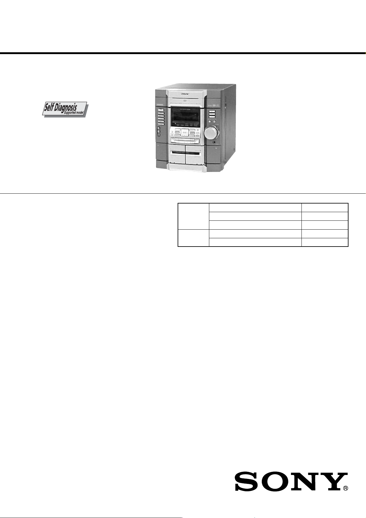
Photo : HCD-R V800D
DVD
Section
Tape deck
Section
SPECIFICATIONS
(4 ohms at 1 kHz, 10%
THD)
(6 ohms at 1 kHz, 10%
THD)
10% THD)
(6 ohms at 1 kHz, 10%
THD)
(4 ohms at 1 kHz, 10%
THD)
Y: 1 Vp-p, 75 ohms
P
B
accepts headphones of
8 ohms or more
16 ohms
24 ohms
24 ohms
MINI HI-FI COMPONENT SYSTEM
US Model
Canadian Model
AEP Model
UK Model
Model Name Using Similar Mechanism NEW
DVD Mechanism Type
Base Unit Name DVBU17
Model Name Using Similar Mechanism NEW
Tape T ransport Mechanism T ype CWM43RR-01
Sub woofer speaker accepts impedance of
Disc player section
System Compact disc and digital
Laser Semiconductor laser
Wavelength 780 – 790 nm
Frequency response DVD (PCM 48 kHz):
, PR: 0.7 Vp-p, 75 ohms
Video color system format
CD OPTICAL DIGITAL OUT
(Square optical connector jack, rear panel)
Wavelength 660 nm
Output Level –18 dBm
— Continued on next page —
CDM58D-DVBU17
12 to 16 ohms
audio and video system
(DVD: λ=650 nm,
CD: λ=780 nm)
Emission duration:
continuous
2 Hz – 22 kHz (±1 dB)
CD: 2 Hz – 20 kHz
(±1 dB)
NTSC, PAL
HCD-GX90D
HCD-RV800D
9-874-118-01
2002I1600-1
© 2002.09
Sony Corporation
Home Audio Company
Published by Sony Engineering Corporation
Page 2
HCD-GX90D/RV800D
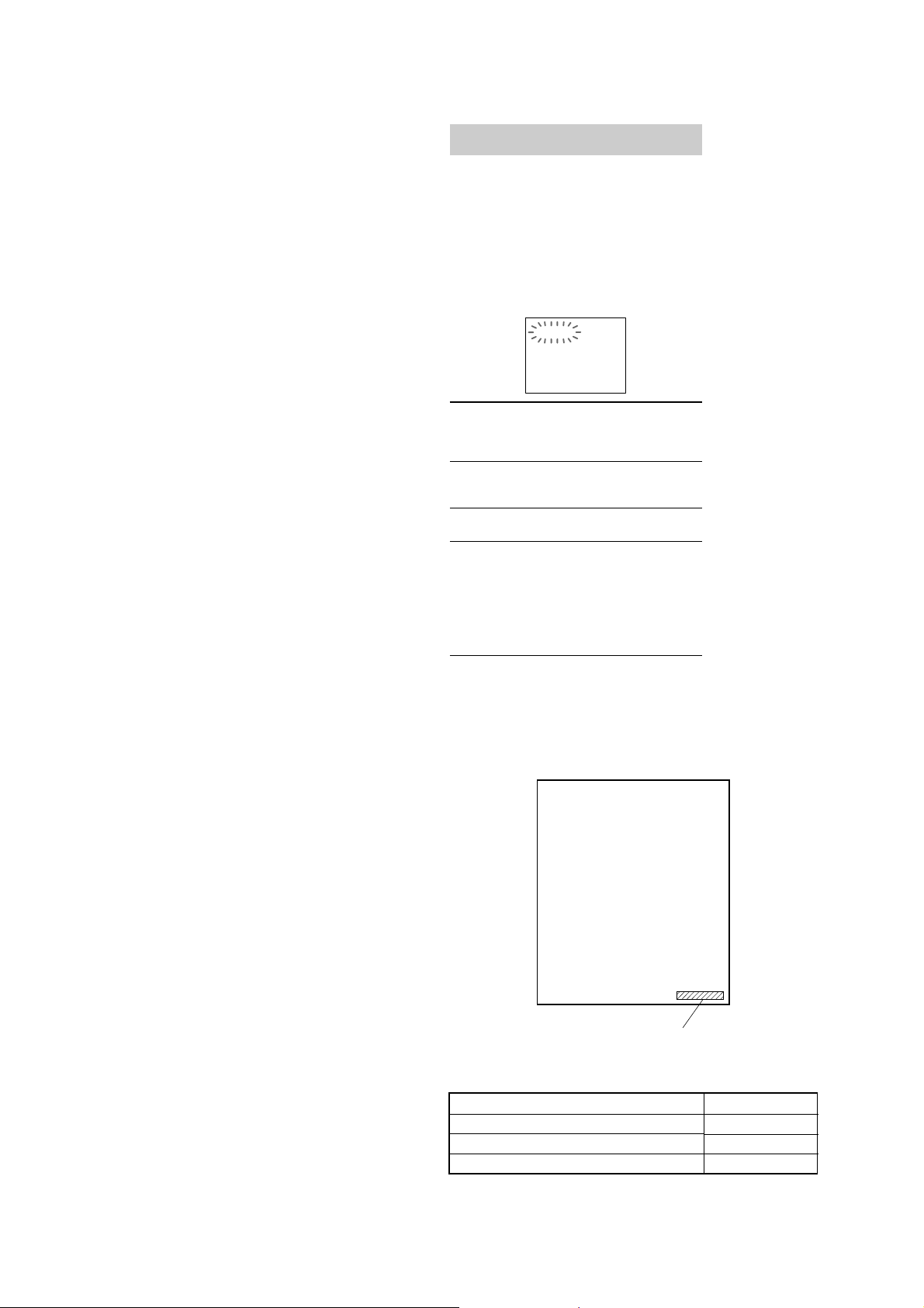
Self-diagnosis function
(When letters/numbers appear in the
display)
When the self-diagnosis function is activated to
prevent the system from malfunctioning, a fivecharacter service number (e.g., C 13 00) with a
combination of a letter and digits appears on
the screen. In this case, check the following
table.
C:13:00
First three
characters of
the service
number
Cause and/or
corrective
action
C 13 The disc is dirty.
, Clean the disc with a soft cloth
(see page 70).
C 31
The disc is not inserted correctly.
, Re-insert the disc correctly.
To prevent a malfunction, the
system has performed the selfdiagnosis function.
, Contact your nearest Sony
dealer or local authorized Sony
service facility and give the
5-character service number.
Example: E 61 10
E XX
(XX is a number)
Tape deck section
Recording system 4-track 2-channel stereo
Frequency response 40 – 13,000 Hz (±3 dB),
Tuner section
FM stereo, FM/AM superheterodyne tuner
FM tuner section
Tuning range 87.5 – 108.0 MHz
Antenna FM lead antenna
Antenna terminals 75 ohm unbalanced
Intermediate frequency 10.7 MHz
AM tuner section
Tuning range
Pan-American models: 530 – 1,710 kHz
European models: 531 – 1,602 kHz (with the
Antenna AM loop antenna
Antenna terminals External antenna terminal
Intermediate frequency 450 kHz
General
Power requirements
North American model: 120 V AC, 60 Hz
European model: 230 V AC, 50/60 Hz
Power consumption
North American model:
HCD-GX90D 270 watts
European model:
HCD-RV800D 270 watts
Dimensions (w/h/d)
HCD-GX90D
HCD-RV800D Approx. 280 × 325 ×
Mass
HCD-GX90D Approx. 11.1 kg
HCD-RV800D Approx. 11.3 kg
Design and specifications are subject to change
without notice.
using Sony TYPE I
cassette
(with the interval set at
10 kHz)
531 – 1,710 kHz
(with the interval set at
9 kHz)
interval set at 9 kHz)
0.25 watts (in Power
Saving Mode)
Approx. 280 × 325 ×
368 mm
370 mm
MODEL IDENTIFICATION
— BACK PANEL —
2
US model
Canadian model
AEP, UK model
MODEL
Parts No.
PARTS No.
4-240-189-0s
4-240-189-1s
4-240-189-2s
Page 3
NOTES ON HANDLING THE OPTICAL PICK-UP
BLOCK OR BASE UNIT
The laser diode in the optical pick-up block may suffer electrostatic
break-down because of the potential difference generated by the
charged electrostatic load, etc. on clothing and the human body.
During repair, pay attention to electrostatic break-down and also
use the procedure in the printed matter which is included in the
repair parts.
The flexible board is easily damaged and should be handled with
care.
NOTES ON LASER DIODE EMISSION CHECK
The laser beam on this model is concentrated so as to be focused on
the disc reflective surface by the objective lens in the optical pickup block. Therefore, when checking the laser diode emission,
observe from more than 30 cm away from the objective lens.
Laser component in this product is capable
of emitting radiation exceeding the limit for
Class 1.
HCD-GX90D/RV800D
TABLE OF CONTENTS
1. GENERAL ·········································································· 4
2. DISASSEMBLY································································ 6
2-1. Case (Top) ····································································· 7
2-2. Lid (DVD)·····································································7
2-3. Front Panel Section······················································· 8
2-4. DVD Mechanism Deck (CDM58D-DVBU17)············· 8
2-5. Tape Mechanical Deck (CWM43RR-01) ····················· 9
2-6. PANEL Board, SUB PANEL Board,
REMOTE Board ························································· 10
2-7. Cassette Holder ··························································· 11
2-8. SUB TRANSFORMER Board, Back Panel,
DC Fan (M961)··························································· 11
2-9. TRANSFORMER Board, MAIN Board····················· 12
2-10. FRONT AMP Board, SURROUND Board,
REG Board·································································· 12
2-11. VIDEO Board, MB Board ·········································· 13
2-12. RF Board, DRIVER Board ········································· 13
2-13. Optical Pick-up ··························································· 14
2-14. MOTOR Board, DIODE Board, SENSOR Board ······ 14
3. TEST MODE ···································································· 15
4. MECHANICAL ADJUSTMENTS ····························· 18
5. ELECTRICAL ADJUSTMENTS ······························· 19
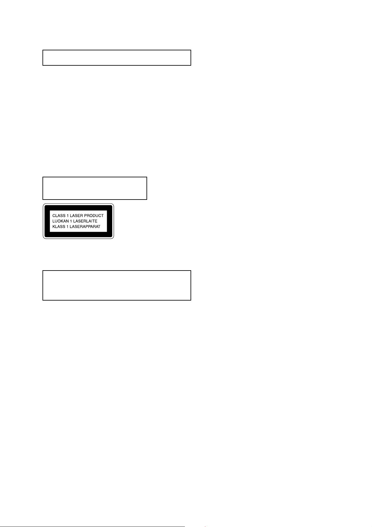
This appliance is classified as a CLASS 1 LASER product. The
CLASS 1 LASER PRODUCT MARKING is located on the rear
exterior.
CAUTION
Use of controls or adjustments or performance of procedures
other than those specified herein may result in hazardous radiation
exposure.
Notes on chip component replacement
•Never reuse a disconnected chip component.
• Notice that the minus side of a tantalum capacitor may be
damaged by heat.
Flexible Circuit Board Repairing
•Keep the temperature of soldering iron around 270˚C
during repairing.
• Do not touch the soldering iron on the same conductor of the
circuit board (within 3 times).
• Be careful not to apply force on the conductor when soldering
or unsoldering.
ATTENTION AU COMPOSANT AYANT RAPPORT
À LA SÉCURITÉ!
LES COMPOSANTS IDENTIFÉS P AR UNE MARQUE 0 SUR LES
DIAGRAMMES SCHÉMA TIQUES ET LA LISTE DES PIÈCES SONT
CRITIQUES POUR LA SÉCURITÉ DE FONCTIONNEMENT. NE
REMPLACER CES COMPOSANTS QUE PAR DES PIÈSES SONY
DONT LES NUMÉROS SONT DONNÉS DANS CE MANUEL OU
DANS LES SUPPÉMENTS PUBLIÉS PAR SONY.
SAFETY-RELATED COMPONENT WARNING!!
COMPONENTS IDENTIFIED BY MARK 0 OR DOTTED LINE WITH
MARK 0 ON THE SCHEMATIC DIAGRAMS AND IN THE PARTS
LIST ARE CRITICAL TO SAFE OPERATION. REPLACE THESE
COMPONENTS WITH SONY PARTS WHOSE PART NUMBERS
APPEAR AS SHOWN IN THIS MANUAL OR IN SUPPLEMENTS
PUBLISHED BY SONY .
6. DIAGRAMS······································································ 21
6-1. Block Diagrams – DVD DSP Section – ···················· 21
– DVD SYS Section – ···················· 22
– Tuner Section –····························23
– Main Section –····························· 24
6-2. Circuit Boards Location·············································· 25
6-3. Printed Wiring Board – RF Board – ··························· 26
6-4. Schematic Diagram – RF Board – ······························ 27
6-5. Printed Wiring Board – MB Board (Side A) – ··········· 28
6-6. Printed Wiring Board – MB Board (Side B) – ··········· 29
6-7. Schematic Diagram – MB Board (1/6) – ···················· 30
6-8. Schematic Diagram – MB Board (2/6) – ···················· 31
6-9. Schematic Diagram – MB Board (3/6) – ···················· 32
6-10. Schematic Diagram – MB Board (4/6) – ···················· 33
6-11. Schematic Diagram – MB Board (5/6) – ···················· 34
6-12. Schematic Diagram – MB Board (6/6) – ···················· 35
6-13. Printed Wiring Board – TC Board – ··························· 36
6-14. Schematic Diagram – TC Board –······························ 37
6-15. Printed Wiring Board – Main Section – ····················· 38
6-16. Schematic Diagram – Main Section (1/3) – ··············· 39
6-17. Schematic Diagram – Main Section (2/3) – ··············· 40
6-18. Schematic Diagram – Main Section (3/3) – ··············· 41
6-19. Printed Wiring Board – VIDEO Board – ···················· 42
6-20. Schematic Diagram – VIDEO Board –·······················43
6-21. Printed Wiring Board – FRONT AMP Board –··········44
6-22. Schematic Diagram – FRONT AMP Board – ············ 45
6-23. Printed Wiring Board – SURROUND Board – ·········· 46
6-24. Schematic Diagram – SURROUND Board – ············· 47
6-25. Printed Wiring Board – Panel Section – ····················· 48
6-26. Schematic Diagram – Panel Section (1/2) – ··············· 49
6-27. Schematic Diagram – Panel Section (2/2) – ··············· 50
6-28. Schematic Diagram – Sensor Section –······················ 51
6-29. Printed Wiring Board – Sensor Section – ··················· 51
6-30. Printed Wiring Board – TRANSFORMER Board –··· 52
6-31. Schematic Diagram – TRANSFORMER Board – ····· 53
6-32. Printed Wiring Board
– SUB TRANSFORMER Board – ····························· 54
6-33. Schematic Diagram
– SUB TRANSFORMER Board – ····························· 55
6-34. IC Pin Function Descriptions······································ 56
7. EXPLODED VIEWS ······················································ 67
7-1. Main Section ······························································· 67
7-2. Front Panel Section····················································· 68
7-3. Chassis Section ··························································· 69
7-4. DVD Mechanism Deck Section
(CDM58D-DVBU17) ················································· 70
8. ELECTRICAL PARTS LIST ······································· 71
3
Page 4
HCD-GX90D/RV800D
Main unit
SECTION 1
GENERAL
This section is extracted from
instruction manual.
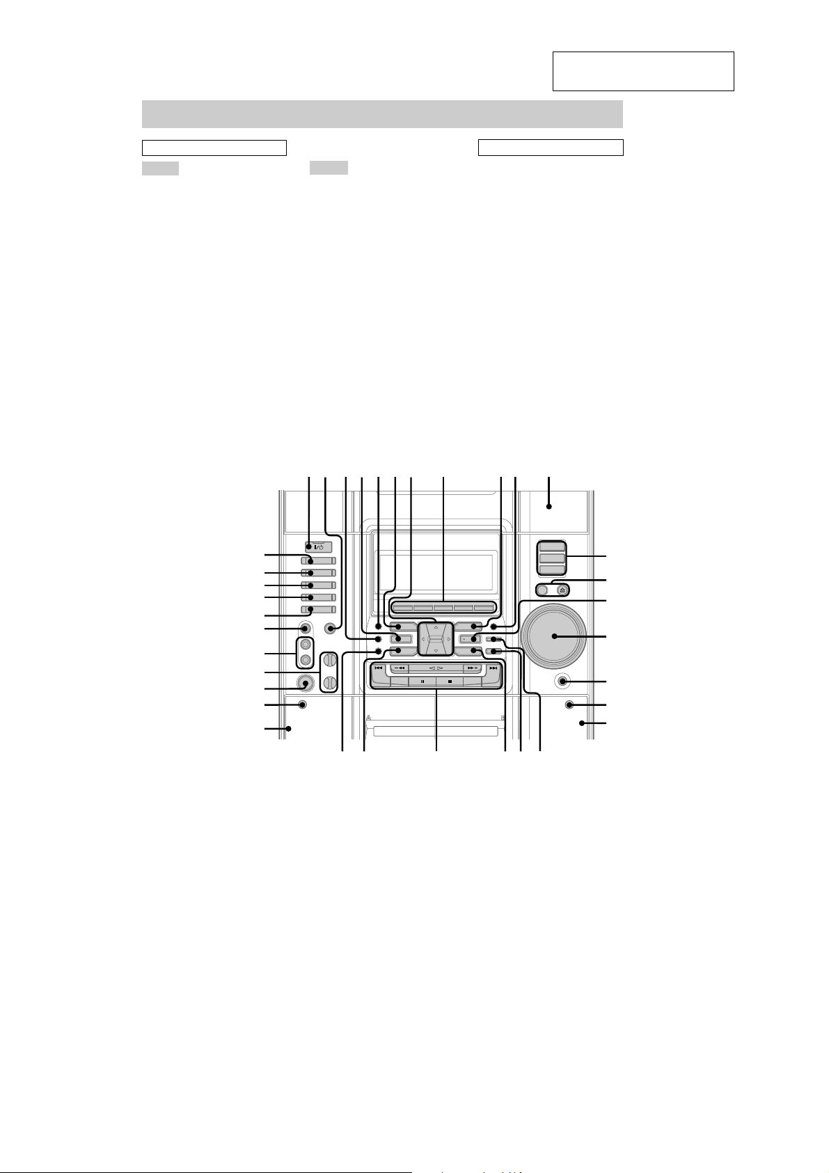
ALPHABETICAL ORDER
A – J
ALBUM+/– ws (19, 20, 26)
AUDIO jacks wl (61)
CD SYNC ql (48, 50)
Deck A wg (47)
Deck B qk (47, 48, 49, 50, 58)
DIRECTION 8 (47, 48, 50, 58)
DISC 1 – 3 qs (18, 19, 20)
DISC SKIP/EX-CHANGE qd (17,
19, 22)
Disc tray qa (17)
DISPLAY 8 (45, 53, 54, 55)
DVD eg (18, 20, 26, 27, 36, 48,
49)
DVD DISPLAY q; (18, 23, 24,
34, 36, 37, 38, 41, 55)
DVD MENU 8 (26)
DVD TOP MENU 8 (26)
ECHO LEVEL control*
EFFECT ON/OFF 4 (51, 52)
ENTER qf (16, 18, 20, 23, 24, 26,
27, 34, 36, 37, 38, 43, 46, 49,
50, 52, 55, 57, 59)
FM MODE 8 (45)
GAME ea (56, 61)
GAME EQ wd (51)
GAME MIXING wf (56)
GROOVE 3 (51)
1
wk (58)
BUTTON DESCRIPTIONS
K – Z
KARAOKE PON*12 (57)
MD (VIDEO)*
MIC jack*
MIC LEVEL control*
MOVIE EQ 9 (51)
MUSIC EQ 6 (51)
P FILE wa (52)
PHONES jack qh
PLAY MODE 8 (18, 20, 49)
PTY*
REC PAUSE/START w; (48, 50,
58)
REPEAT 8 (23)
SURROUND*
TAPE A/B ed (47, 48, 58)
TUNER MEMORY 8 (43)
TUNER/BAND ef (43, 44)
VIDEO jack e; (61)
VIDEO (MD)*
VOLUME control qg (33, 53, 59)
4
8 (46)
3
wj (57)
2
es (62)
5
5 (53)
6
es (62)
3
wk (57)
?/1 (power) 1
v/V/b/B 7
Z OPEN/CLOSE qd
Z PUSH (deck B) qj
– m/M + ws
hH ws
./> ws
X ws
x ws
Z PUSH (deck A) wh
1
MHC-RV900D (except for
*
Latin American model) and
RV600D/RV600DJ (except
for Latin American model)
only
2
except for MHC-GX90D
*
3
*
MHC-RV900D and RV600D/
RV600DJ only
4
*
European model only
5
MHC-RV600D/RV600DJ only
*
6
*
MHC-GX90D only
12 34567 098qa
eg
ef
ed
es
ea
e;
wl
wk
wj
wh
wg
qs
qd
qf
qg
qh
qj
qk
wswdwf
qlw;wa
4
Page 5
HCD-GX90D/RV800D
Remote control
ALPHABETICAL ORDER
A – M
ALBUM +/– wd wl (19, 20, 26)
AMP MENU wa (57)
ANGLE w; (37)
AUDIO ed (35)
CLEAR qf (20, 22, 24, 25, 31)
CLOCK/TIMER SELECT 2
(51, 60)
CLOCK/TIMER SET 3 (16, 50,
59)
DISC +/– wg wj (19, 20, 22)
DISPLAY qa (45, 53, 54, 55)
DVD rs (18, 20, 21, 26, 27, 28,
36, 48, 49)
DVD DISPLAY qd (18, 23, 24,
34, 36, 37, 38, 41, 55)
DVD MENU ef (26)
DVD SETUP ek (28, 33, 40)
DVD TOP MENU ef (26)
EFFECT ON/OFF es (51, 52)
ENTER wk (16, 18, 20, 21, 23,
24, 26, 27, 28, 33, 34, 36, 37,
38, 40, 43, 46, 49, 50, 52, 55,
57, 59)
GAME 8 (56, 61)
GAME EQ e; (51)
GAME MIXING 0 (56)
GROOVE es (51)
MD (VIDEO) 9 (62)
MOVIE EQ e; (51)
MULTI ROOM* ea
MUSIC EQ e; (51)
12345
rf
rd
rs
ra
r;
el
ek
ej
eh
eg
ef
ed
es
ea
e;
wl
N – Z
NEXT eh (18, 27)
Number buttons qs (19, 27, 39,
40, 42, 49)
P FILE ws (52)
PLAY MODE r; (18, 20, 21, 49)
PRESET +/– eh (43, 44)
PREV eh (18, 27)
REPEAT el (23)
RETURN O ej (27, 39, 41)
SCAN/SLOW
SLEEP 1 (59)
SUBTITLE ql (38)
SURROUND es (53)
TAPE rd (47, 48)
TUNER/BAND ra (43, 44)
TUNING +/– eg (43, 45)
TV ?/1 4 (15)
TV CH +/– rf (15)
TV/VIDEO 7 (15)
TV VOL +/– 6 (15)
VOL +/– wf (33, 53, 59)
BUTTON DESCRIPTIONS
?/1 (power) 5
x qg
nN qh
X qj
M/m/</, wh
m eg
M eg
. eh
> eh
* This button does not function.
/ qk (19)
6
7
8
9
0
qa
qs
qd
qf
qg
qh
qj
qk
ql
w;
wa
ws
wd
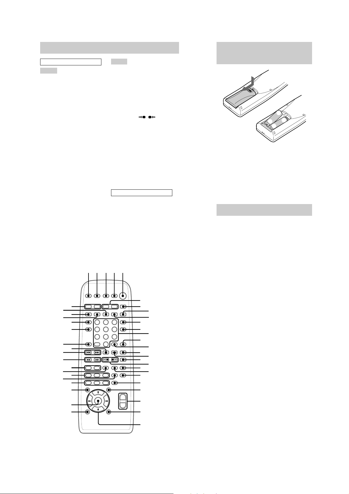
Inserting two R6 (size AA)
batteries into the remote
e
E
E
e
Tip
With normal use, the batteries should last for about
six months. When the remote no longer operates the
system, replace both batteries with new ones.
Note
If you do not use the remote for a long period of time,
remove the batteries to avoid possible damage from
battery leakage.
Setting the clock
1
Press ?/1 to turn on the system.
2
Press CLOCK/TIMER SET on the
remote.
3
Press M or m on the remote repeatedly
to set the hour.
4
Press , on the remote.
The minute indication flashes.
5
Press M or m on the remote repeatedly
to set the minute.
6
Press ENTER.
The clock starts working.
To adjust the clock
1
Press CLOCK/TIMER SET on the remote.
2
Press M or m on the remote repeatedly to
select “CLOCK SET”, then press ENTER.
3
Do the same procedures as step 3 to 6
above.
Note
The clock settings are canceled when you disconnect
the power cord or if a power failure occurs.
wk
wj
wf
wg
wh
5
Page 6
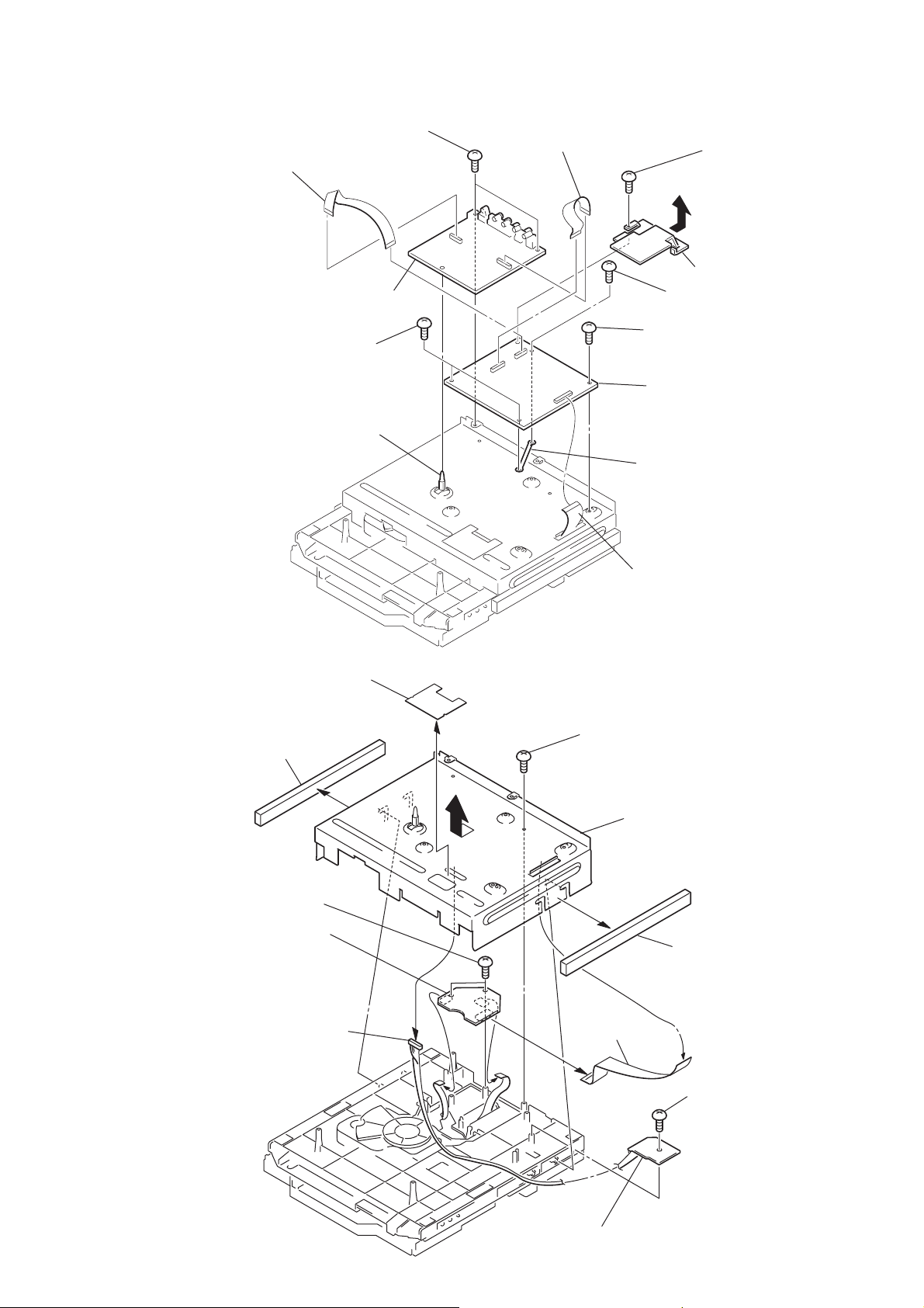
HCD-GX90D/RV800D
SECTION 2
DISASSEMBLY
• The equipment can be removed using the following procedure.
FRONT PANEL SECTION
SET
CASE (TOP)
DVD LID
TAPE MECHANISM DECK
(CWM43RR-01)
PANEL BOARD, SUB PANEL BOARD,
REMOTE BOARD
CASSETTE HOLDER
DVD
MECHANISM DECK BLOCK
SUB TRANSFORMER BOARD,
BACK PANEL, DC FAN (M961)
TRANSFORMER BOARD,
MAIN BOARD
FRONT AMP BOARD,
SURROUND AMP BOARD,
REG BOARD
Note : Follow the disassembly procedure in the numerical order given.
VIDEO BOARD, MB BOARD
RF BOARD, DRIVER BOARD
OPTICAL PICK-UP
MOTOR BOARD, DIODE BOARD,
TRAY, SENSOR BOARD
6
Page 7
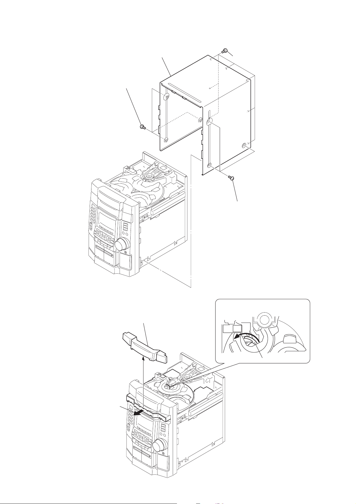
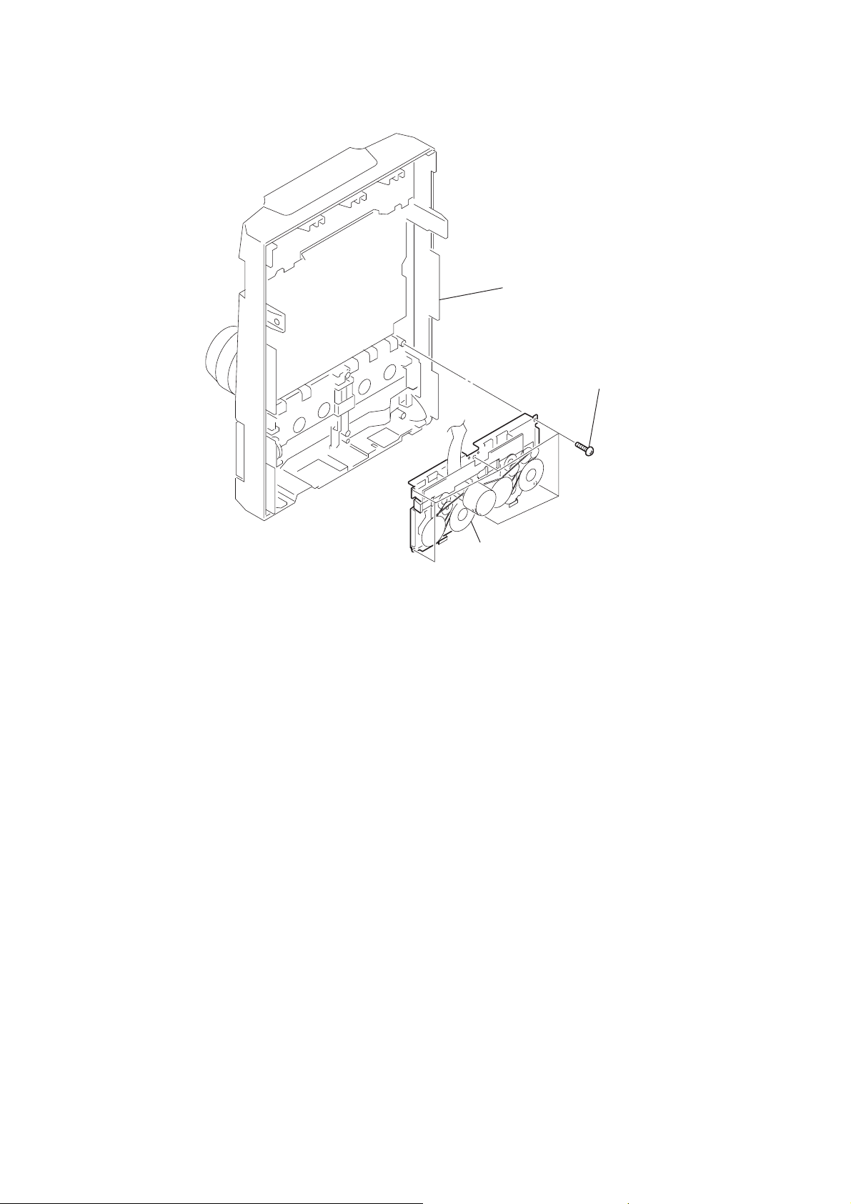
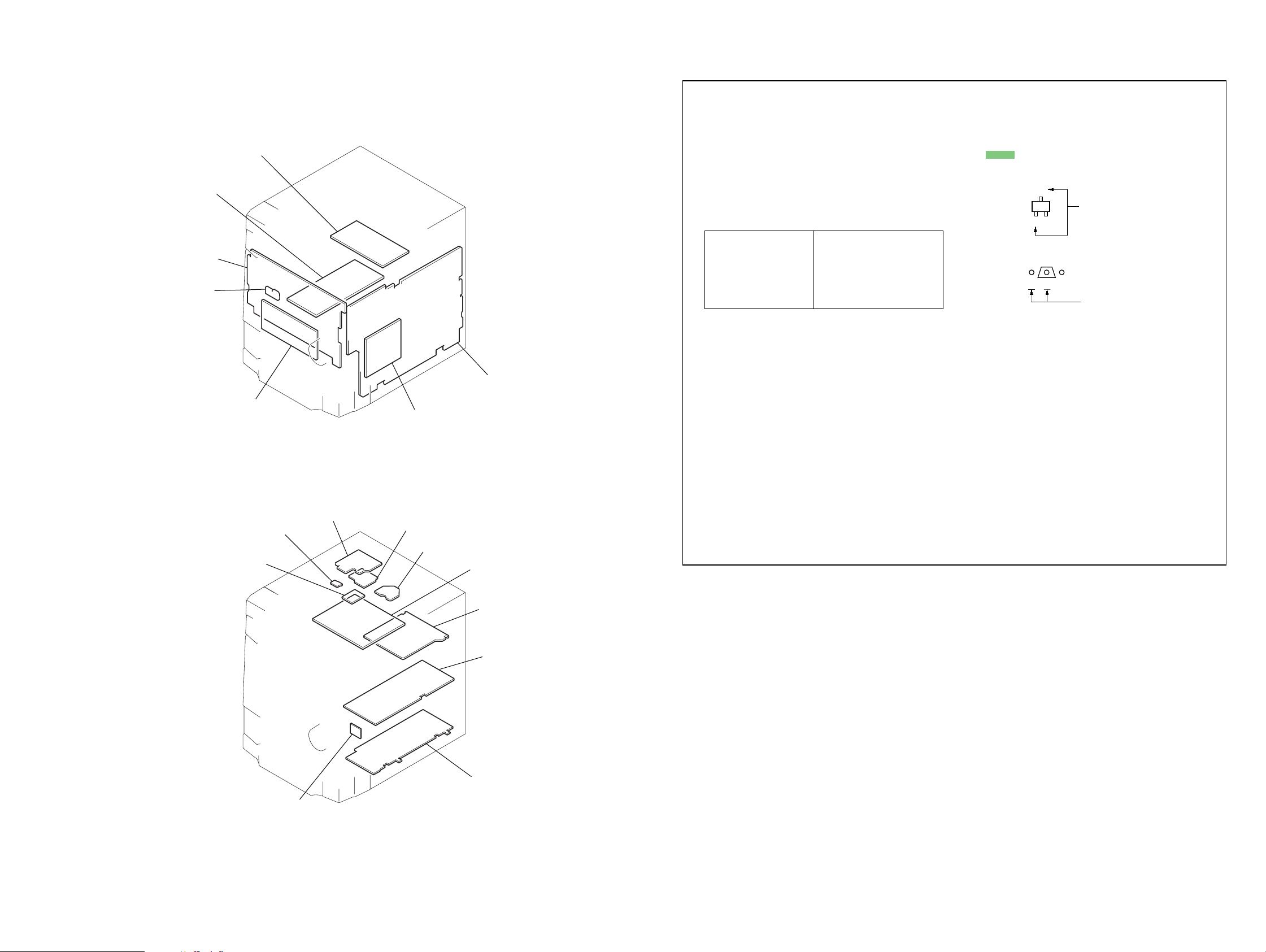
Note: Follow the disassembly procedure in the numerical order given.
)
2-1. Case (Top)
2
three screws (case 3 TP2)
4
case
HCD-GX90D/RV800D
3
seven screws (BVTT 3
×
6
2-2. Lid (DVD)
4
lid (DVD)
3
1
three screws (case 3 TP2)
DVD mechanism deck (CDM58D-DVBU17)
1
T
urn the pulley to the direction of arrow.
pulley
2
Pull-out the disc tray.
7
Page 8
HCD-GX90D/RV800D
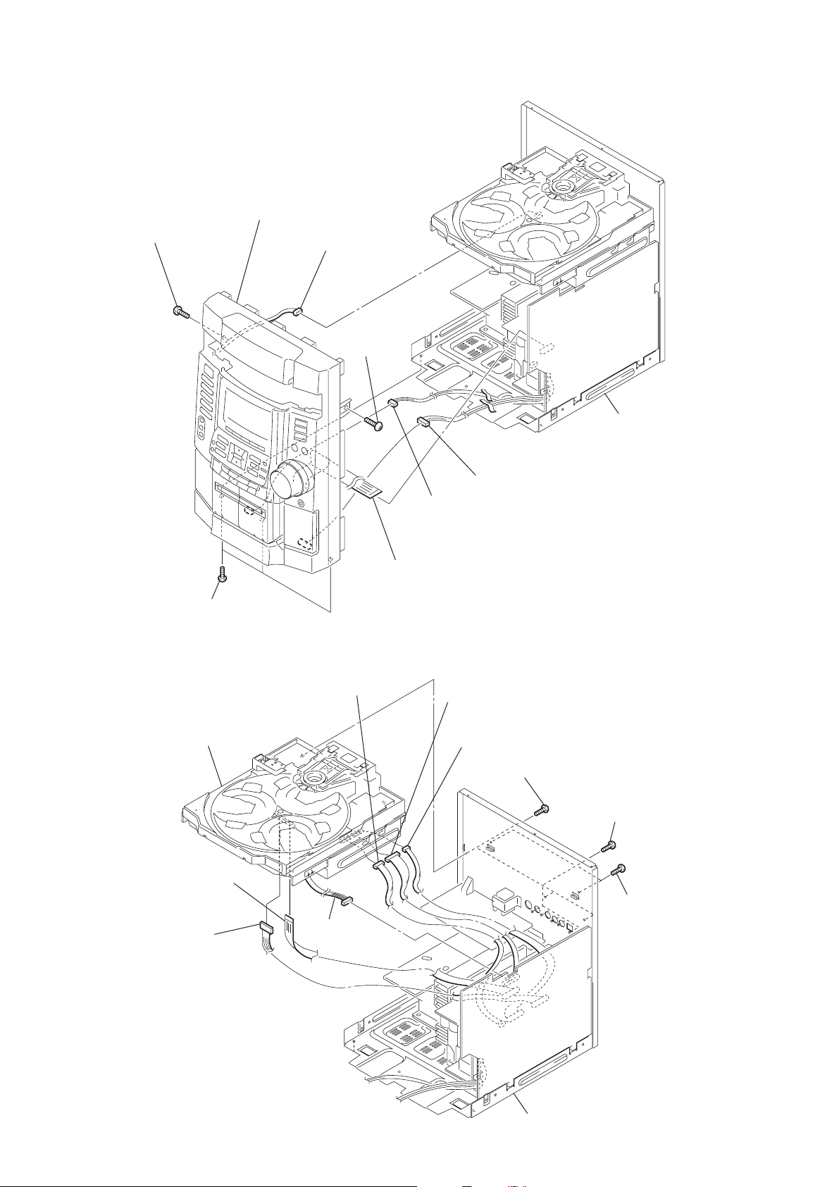
2-3. Front Panel Section
4
screw (BVTP 3
×
8
front panel section
8)
1
connector (CN502)
3
screw
(BVTP 3
×
8)
chassis section
5
three screws (BVTP 3
×
8)
2-4. DVD Mechanism Deck (CDM58D-DVBU17)
4
connector (CN103)
0
DVD mechanism deck
(CDM58D-DVBU17)
2
flat type wire (CN104)
6
connector (CN602)
2
flat type wire (CN605)
5
connector (CN505)
6
connector (CN508)
7
connector (CN603)
7
three
screws (BVTP 3
×
8)
9
five
screws
(BVTP 3
×
8)
8
two
screws
×
8)
1
connector (CN103)
3
connector
(CN709)
(BVTP 3
chassis section
8
Page 9
)
2-5. Tape Mechanical Deck (CWM43RR-01)
panel section
1
six
screws (BVTP 2.6
HCD-GX90D/RV800D
×
8
2
tape mechanism deck
(CWM43RR-01)
9
Page 10
HCD-GX90D/RV800D
2-6. PANEL Board, SUB PANEL Board, REMOTE Board
1
volume knob
6
two claws
front panel
qf
SUB PANEL board
5
qs
four screws
(BVTP 2.6
two claws
×
8)
9
REMOTE board
8
connector (CN1006)
3
five screws
(BVTP 2.6
×
8)
2
Remove the
three solderings
10
qd
two screws
(BVTP 2.6
×
8)
qa
connector (CN1002)
0
connector (CN1003)
4
six screws
(BVTP 2.6
×
8)
7
PANEL board
Page 11
)
2-7. Cassette Holder
8
cassette, holder (R)
4
cassette, holder (L)
6
HCD-GX90D/RV800D
3
cassette door, spring (B)
2
1
5
7
cassette door, spring (A)
2-8. SUB TRANSFORMER Board, Back Panel, DC Fan (M961)
qf
back panel
1
connector (CN901)
2
connector (CN902)
qa
SUB TRANSFORMER board
3
connector (CN903)
0
three
(BVTP 3
screws
panel section
×
8)
7
(BVTP 3
two
screws
5
(BVTP 3
6
(BVTP 3
8
(BVTP 3
×
8)
qs
two
screws
(BVTP 3
five
screws
×
three
screws
×
two
screws
×
×
8)
8
8)
8)
chassis section
qd
dc fan (M961)
4
connector (CN704)
9
four
screws
(BVTP 3
×
8)
11
Page 12
HCD-GX90D/RV800D
)
2-9. TRANSFORMER Board, MAIN Board
0
(BVTP 3
6)
two
6
TRANSFORMER board
4
two
screws
(BV 4
3
connector
(CN913)
2
connector
(CN915)
1
connector
(CN914)
5
two
(BV 4
×
8)
9
two
screws
(BVTT 3
screws
×
8)
×
screws
×
qa
qs
two claws
cover (heat sink)
8
three
(BVTT 3
screws
qg
×
6)
qj
SURROUND board and
FRONT AMP board assy
TC board
qd
connector (CN609)
qf
connector (CN608
8)
2-10.FRONT AMP Board, SURROUND Board, REG Board
4
bracket (PWB)
heat sink assy
2
bracket (PWB)
1
two
screws
×
(BVTP 3
8)
3
three
(BVTP 3
screws
×
8)
qh
qs
SURROUND board
MAIN board
9
four
screws
(BVTP 3
7
connector (CN302)
7
two
screws
(BVTP 3
8
two
screws
(BVTP 3
×
16)
×
×
8)
8)
12
6
REG board
5
s
crew
(BVTP 3
×
8)
qd
FRONT AMP board
0
five
screws
(BVTP 3
×
qa
two
screws
(BVTP 3
8)
×
16)
Page 13
)
)
2-11.VIDEO Board, MB Board
1
flat type wire (CN501,CN202)
9
(BVTP 3
4
PWB holder
two
screws
3
two
screws
(BVTP 3
5
VIDEO board
×
8)
×
HCD-GX90D/RV800D
2
8)
flat type wire
(CN503,CN302)
qs
(BVTP 3
8
screw
(BVTP 3
qf
MB board
qd
bracket (AL)
7
screw
(BVTP 3
0
qa
heat sink (DVD
screw
×
×
6)
×
6)
8)
2-12.RF Board, DRIVER Board
7
cushion (DVD)
two
screws (PTP 2.6
qa
qs
RF board
×
12)
2
cushion (A)
3
1
screw
(BVTP 3
8
6
flat type wire (CN501)
×
8)
bracket (DVD)
6
cushion (DVD)
5
connector
0
9
4
flat type wire
qf
DRIVER board
qd
screw (BVTP 2.6
×
8
13
Page 14
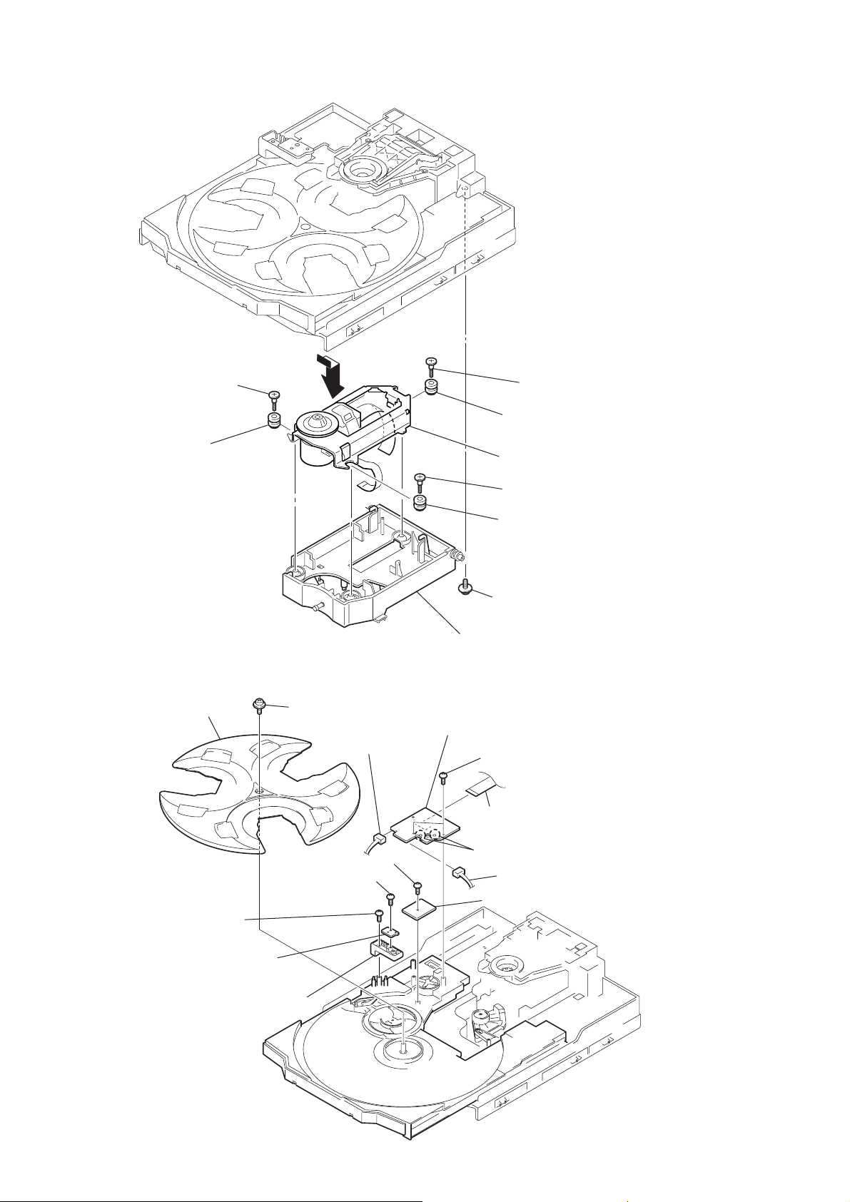
HCD-GX90D/RV800D
)
2-13.Optical Pick-up
3
6
step
screw (L)
insulator
2
2-14.MOTOR Board, DIODE Board, SENSOR Board
qa
qs
tray (DVD)
screw (PTPWH 2.6
5
connector (CN723)
×
4
step
screw (L)
7
insulator
9
optical pick-up
5
step
screw (L)
8
insulator
1
floating
screw (PTPWH M2.6
0
holder (DBU1) assy
8)
6
MOTOR board
1
two
screws (BVTP 2.6
×
8)
14
9
screw (BVTP 2.6
×
8)
8
DIODE board
0
qd
screw (BVTP 2.6
7
screw (BVTP 2.6
bracket (sensor)
×
×
3
flat type wire (CN721)
2
8)
8)
Remove the two solderings of motor.
4
connector (CN722)
qf
SENSOR board
Page 15
SECTION 3
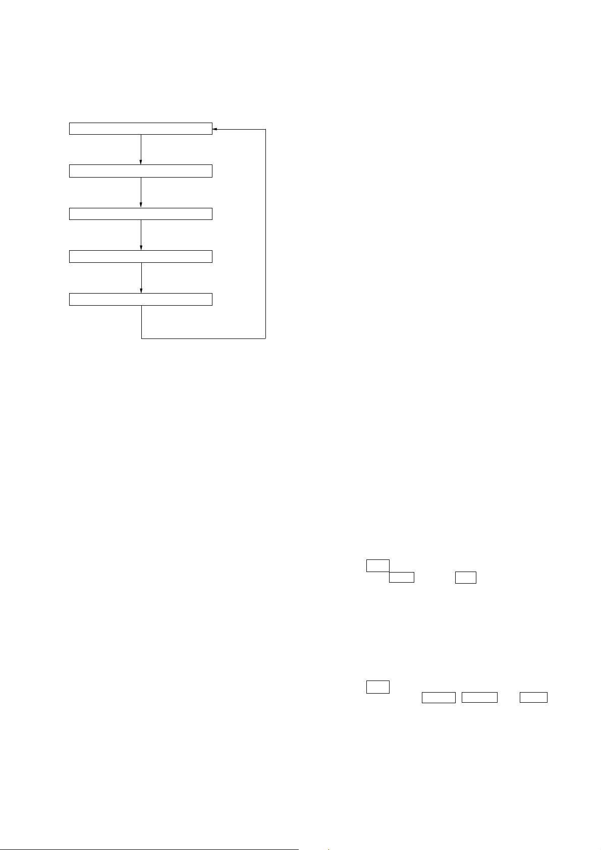
TEST MODE
HCD-GX90D/RV800D
[Cold Reset]
• The cold reset clears all data including preset data stored in the
RAM to initial conditions. Execute this mode when returning
the set to the customer.
Procedure:
1. Press three buttons x , ENTER , and ?/1 simultaneously.
2. The fluorescent indicator tube display “COLD RESET” and
the set is reset.
[Hot Reset]
1. Press three buttons x , GAME EQ , and DISPLAY simulta-
neously.
2. The fluorescent indicator tube becomes blank instantaneously,
and the set is reset
[T uner Step Change] (Except for European and Middle Eastern
models)
•A step of AM channels can be changed ov er between 9 kHz and
10 kHz.
Procedure:
1. Press `/1 button to turn the set ON.
2. Select the function “TUNER”, and press TUNER/BAND button
to select the BAND “AM”.
3. Press `/1 button to turn the set OFF.
4. Press ENTER and `/1 buttons simultaneously, and the display
of fluorescent indicator tube changes to “AM 9 k STEP” or
“AM 10 k STEP”, and thus the channel step is changed over.
[VIDEO/MD Function Change]
• Change of function VIDEO or MD ( also the input le vel changes).
Procedure:
1. Press `/1 button to turn the set ON.
2. Press VIDEO (MD) and `/1 buttons simultaneously, and the
display of fluorescent indicator tube changes to “MD” or
“VIDEO”, and thus the channel step is changed over.
3. Press `/1 button to turn the set OFF.
[GC Test Mode]
•This mode is used to check the FL tube, LED, keyboard, volume and phones.
Procedure:
1. Press three buttons x , GAME EQ , and DISC 2 simulta-
neously.
2. LEDs and fluorescent indicator tube are all turned on.
3. Press simultaneously the two buttons of GAME EQ and DISC
2 . Whenever these tw o buttons are pressed simultaneously , the
mode changes from Key check, Ke y count c heck, Headphones
input check and Volume check in this order.
4. When the Key check mode is entered, the display shows the
indication of “KEY 0 0 0”.
The keys that are assigned to the respective channels of the ke y
entry signal lines (KEY0, KEY1, KEY2) that are input to IC001
Display Controller on the panel board, are checked. While you
press the button, the number that corresponds to the key shown
in the table below, is displayed in the location of the
corresponding channel. (The ?/1 and DISPLAY buttons are
not included in these channels.)
Display
1DVD X DISC 1
2 TUNER/BAND x DISC 2
3TAPE A/B ALBUM + DISC 3
4 VIDEO (MD) >Z OPEN/CLOSE
5 GAME M +
6— g G
7DVD MENU – m
8 GAME EQ ALBUM –
9 MUSIC EQ . CD SYNC
10
11 GAME MIXING V P FILE
12 GROOVE B ENTER
13 — v MOVIE EQ
14 — — DVD DISPLAY
Left Center Right
(KEY0) (KEY1) (KEY2)
EX-CHANGE
TUNER MEMORY
PLAY MODE
DVD TOP MENU
EFFECT ON/OFF
b
PAUSE/START
DISC SKIP/
FM MODE
REPEAT
DIRECTION
REC
5. When the Key count check mode is entered, the display shows
the indication of “KEY 0 1”.
Whenever the button is pressed, number in the first digit
increments. (RV90D: 38) At the same time, only when the key
is being pressed, the KEY channel is displayed in the second
digit. (KEY0: 1, KEY1: 2, KEY2: 3)
(The buttons that are already pressed once and the buttons of
?/1 and DISPLAY are not counted.)
6. When the Headphones input check mode is entered, the display
shows the indication of “H_P OFF” or “H_P ON” depending
on the PHONES jack status.
7. When the Volume check mode is entered, the display shows the
indication of “VOLUME FLAT” or “VOLUME DOWN” or
“VOLUME UP” depending on the VOLUME status.
8. You can exit the Test Mode when you press the GAME EQ
and DISC 2 buttons simultaneously.
15
Page 16
HCD-GX90D/RV800D
[MC Test Mode]
•This mode is used to check operations of the respective sections
of Amplifier, Tuner , and Tape.
Procedure:
•To enter MC Test Mode
1. Press `/1 button to turn on the set.
2. Press the three buttons of x , GAME EQ and DISC 3 simul-
taneously.
* Check of Amplifier
Initial settings: Input , GAME
EQ , FLAT
Mode , MUSIC
VA CS , OFF
Output channel switching:
MUSIC key: L , LR , R through
MOVIE key: L , SL R , SR through
GAME key:L , L, SL, C R , R, SR, SW through
TOOL MODE key: L , CR , SW through
1. When VOLUME control knob is turned clockwise even
slightly, the sound volume increases to is maximum and a
message “VOLUME MAX” appears for two seconds, then the
display returns to the original display.
2. When VOLUME control knob is tuned counter-clockwise
even slightly, the sound v olume decreases to its minimum and a
message “VOLUME MIN” appears for two seconds, then the
display returns to the original display.
3. When you press the v button, the message “GEQ MAX” is
displayed and the entire band of the graphic equalizer is set to
the maximum level.
4. When you press the V button, the message “GEQ MIN” is
displayed and the entire band of the graphic equalizer is set to
the minimum level.
5. When you press the b , B or P FILE button, the message
“GEQ FLT” is displayed and the entire band of the graphic
equalizer is set to the center level.
6. Whenever you press the ENTER button, it toggles between
“VACS ON” and “VAC OFF” so that you can switch ON or
OFF of VACS.
*To return to normal mode again.
1. When you want to exit this mode, press `/1 button.
2. The cold reset is enforced at the same time.
[Aging Mode]
This mode can for operation check of tape deck section.
• If an error occurred:
The aging operation stops and display then status.
• If no error occurs:
The aging operation continues repeatedly.
Procedure:
1. Press the DVD button to select the function “DVD”.
2. Load the tapes into the decks A and B respectively.
3. Set a disk in “DISK1” tray.
4. Press the PLA Y MODE button to set the “ALL DISCS” mode,
and press the REPEAT button to “REPEAT” off.
5. Press three buttons of x , GAME EQ , and DISC SKIP/EX-
CHANGE simultaneously.
6. The florescent indicator tube display “AGING”, aging mode
start.
7. To exit from the aging mode, operate the cold reset.
•The sequence during the aging mode is following as below.
• If an error occurred, stop display that step.
Aging mode sequence (Tape deck section):
Rewind the tape A
“T APE A A G-1”
Shut off
Rewind the tape B
“T APE A A G-2”
Shut off
FWD play the tape A
“T APE A A G-3”
2 minutes
Fast forward the tape A
“T APE A A G-4”
Shut off or 20 seconds
RVS play the tape A
“T APE A A G-5”
2 minutes
Rewind the tape A
“T APE A A G-6”
Shut off
16
FWD play the tape B
“TAPE B AG-3”
2 minutes
Fast forward the tape B
“TAPE B AG-4”
Shut off or 20 seconds
RVS play the tape B
“TAPE B AG-5”
2 minutes
Rewind the tape B
“TAPE B AG-6”
Shut off
Page 17
HCD-GX90D/RV800D
[DVD Service Mode]
•The sequence during the aging mode is following as below.
Aging mode sequence (DVD section):
Tray Turn
Disc 1 Chucking
TOC Read
Track 1 Play
2 seconds
Last Track Play
2 seconds
Error History Display
1. BD Error History Display
11 digits are displayed after the D character.
Example of display : D00209010100
1st digit : Indicates the error history number.
0 is the latest error
2nd to 3rd digits : Indicates details of the problem.
01 : Cannot focus
02 : GFS NG
03 : Start time over
04 : Focus deviates continuously
05 : Q code absent for some time
4th to 5th digits : Processing when problems occur
01 : Currently SHIP processing
02 : Currently POWER OFF processing
03 : Currently initializing
04 : Currently stopping
05 : Currently STOP operation processing
06 : Currently start processing
07 : Currently TOC reading
08 : Currently searching
09 : Currently playing
0A : Currently pausing
0B : Currently PLAY manual searching
0C : Cur rently PAUSE manual searching
6th to 7th digits : Operations currently performed for problems
which have occurred
8th to 9th digits : Rotation speed of DISC when problems occur
01 : x1 speed
02 : x2 speed
10th to 11th digits : Fixed at 00
2. CDM Error History <CDM58D Error History Display>
11 digits are displayed after the M character.
Example of display : M0FF400220000
1st digit : Indicates the error history number.
0 is the latest error
2nd to 3rd digits : Indicates the details of the problem.
01 : Initialization table is currently rotating 1
02 : Initialization table is currently rotating 2
03 : Initialization table is currently rotating 3
04 : Currently DISC SKIP in OPEN mode
05 : CLOSE table is currently rotating
06 : Chucking table is currently rotating
07 : Currently performing SHIP operations
08 : Currently performing release operations
09 : Currently performing POWER OFF
operations
4th to 5th digits : Processing when problems occur
01 : Currently performing SHIP operations
02 : Currently performing POWER OFF
operations
03 : Currently initializing
04 : Currently performing release operations
05 : Currently in chuck stop state
06 : Currently performing CLOSE operations
07 : Currently performing exchange CLOSE
operations
08 : Currently performing OPEN operations
09 : Currently performing OPEN POP UP
operations
0A: Currently performing exchange OPEN
operations
6 to 7th digits : Operations currently performed for problems
which have occurred
8th to 9th digits : Targets of processing when problems occur
Same as 4th to 5th digits
10th to 11th digits : Fixed at 00
[DVD and CD Ship Mode (No Memory Clear)]
•This mode moves the position to the position durable to vibration Use this mode when returning the set to the customer after
repair.
Procedure:
1. Press `/1 button to turn the set ON.
2. Press three DVD button and
3. After the “STANBY” display blinks six times, a message
“LOCK” is displayed on the fluorescent indicator rube, and the
DVD ship mode is set.
[DVD and CD Ship Mode (Memory Clear)]
•This mode moves the pickup to the position durable to vibration. Use this mode when returning the set to the customer after
repair.
Procedure:
1. Press
2. Press three buttons ENTER , DISC 1 , and DVD button
simultaneously.
3. After the “STANDBY” display blinks six times, a message
“LOCK” is displayed on the fluorescent indicator tube, and the
DVD ship mode is set.
button to turn the set ON.
`/1
button simultaneously.
`/1
17
Page 18
HCD-GX90D/RV800D
SECTION 4
MECHANICAL ADJUSTMENTS
[REPEAT 5 LIMIT OFF MODE]
•This mode is used to enable infinite repetitions.
Normally, the number of repetitions allowed is 5.
Procedure:
1. Press
2. Set the function “DVD”.
3. Press three burtons x , MUSIC EQ and DISC 2 is simulta-
neously.
4. Infinite repetitions is enabled.
5. This state is maintained ( memorized ) until COLD RESET is
executed.
button to turn ON the power supply.
`/1
Precaution
1. Clean the following parts with a denatured alcohol-moistened
swab:
record/playback heads pinch rollers
erase head rubber belts
capstan idlers
2. Demagnetize the record/playback head with a head
demagnetizer.
3. Do not use a magnetized screwdriver for the adjustments.
4. After the adjustments, apply suitable locking compound to the
parts adjusted.
5. The adjustments should be performed with the rated power
supply voltage unless otherwise noted.
Torque Measurement
Mode
FWD
FWD
back tension
REV
REV
back tension
FF/REW
FWD tension
REV tension
Torque meter
CQ-102C
CQ-102C
CQ-102RC
CQ-102RC
CQ-201B
CQ-403A
CQ-403R
Meter reading
3.06 N • m to 6.96 N • m
31 to 71 g • cm
(0.43 – 0.98 oz • inch)
0.19 N • m to 0.58 N • m
2 to 6 g • cm
(0.02 – 0.08 oz • inch)
3.06 N • m to 6.96 N • m
31 to 71 g • cm
(0.43 – 0.98 oz • inch)
0.19 N • m to 0.58 N • m
2 to 6 g • cm
(0.02 – 0.08 oz • inch)
6.96 N • m to 14.02 N • m
71 to 143 g • cm
(0.98 – 1.99 oz • inch)
9.80 N • m
100 g or more
(3.53 oz or more)
9.80 N • m
100 g or more
(3.53 oz or more)
18
Page 19
SECTION 5
r
MAIN
board
CN607
set
test tape
P-4-A100
(10 kHz, –10 dB)
pin
7
oscilloscope
L-CH
R-CH
V
H
waveform of oscilloscope
in phase 45°90°135°180
°
good
wrong
pin
6
pin
5
L
R
forward
reverse
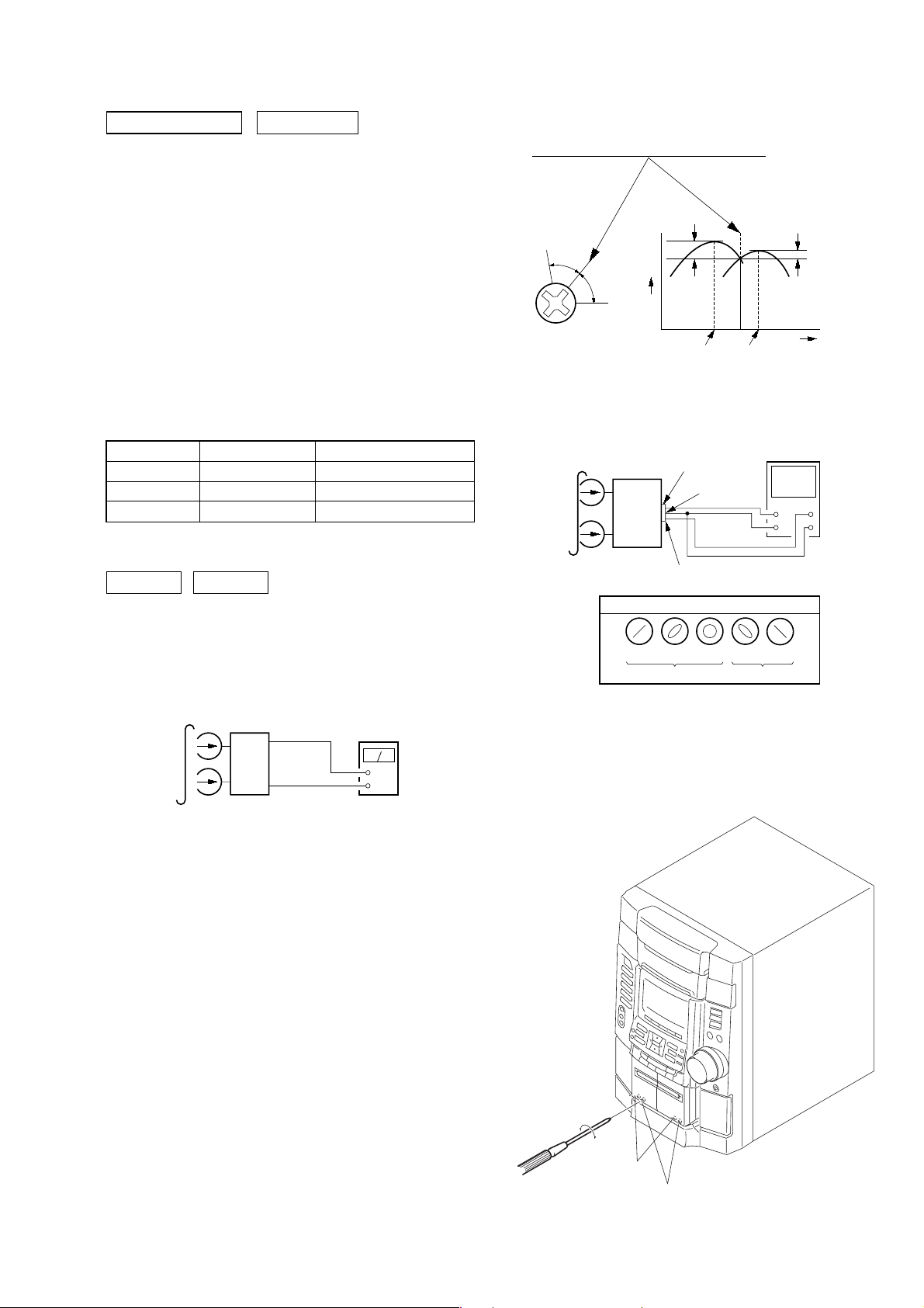
ELECTRICAL ADJUSTMENTS
HCD-GX90D/RV800D
DECK SECTION
0 dB=0.775 V
1. Demagnetize the record/playback head with a head
demagnetizer.
2. Do not use a magnetized screwdriver for the adjustments.
3. After the adjustments, apply suitable locking compound to the
parts adjust.
4. The adjustments should be performed with the rated power
supply voltage unless otherwise noted.
5. The adjustments should be performed in the order given in this
service manual. (As a general rule, playback circuit adjustment
should be completed before performing recording circuit
adjustment.)
6. The adjustments should be performed for both L-CH and RCH.
7. Switches and controls should be set as follows unless otherwise
specified.
•Test Tape
Tape Signal Used for
P-4-A100 10 kHz, –10 dB Azimuth Adjustment
WS-48B 3 kHz, 0 dB Tape Speed Adjustment
P-4-L300 315 Hz, 0 dB Level Adjustment
Record/Playback Head Azimuth Adjustment
DECK A DECK B
2. Turn the adjustment screw and check output peaks. If the peaks
do not match for L-CH and R-CH, turn the adjustment screw
so that outputs match within 1dB of peak.
Output
level
within
1dB
L-CH
peak
R-CH
peak
within
1dB
Screw
position
L-CH
peak
Screw
position
R-CH
peak
3. Mode: Playback
Note: Perform this adjustments for both decks
Procedure:
1. Mode: Playback
test tape
P-4-A100
(10 kHz, –10 dB)
set
main board
CN607
Pin
5
(L-CH)
7
(R-CH)
Pin
main board
CN607
6
(GND)
Pin
level mete
+
–
4. After the adjustments, apply suitable locking compound to the
pats adjusted.
Adjustment Location: Playback Head (Deck A).
Record/Playback/Erase Head (Deck B).
19
Page 20
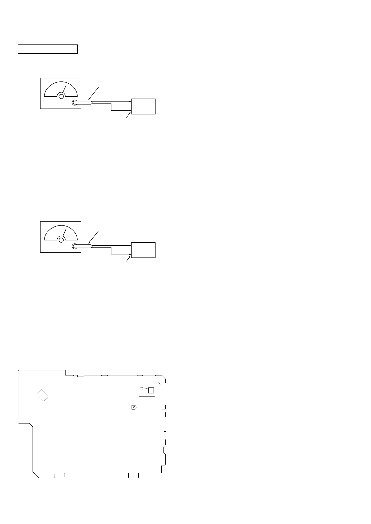
HCD-GX90D/RV800D
TUNER SECTION
FM Tuned Level Adjustment
FM RF SSG
Ω
coaxial
75
set
Carrier frequency : 98 MHz
Modulation : AUDIO 1 kHz, 75 kHz
deviation (100%)
Output level : 25 dB (at 75
Ω
open)
Procedure:
1. Supply a 25 dB 98 MHz signal from the ANTENN A terminal.
2. Tune the set to 98 MHz.
3. Adjust R V11 to the point (moment) when the TUNED indicator
will change from going off to going on.
Adjustment Location: MAIN board
FM ANTENNA terminal
(TM1)
Null Adjustment
FM RF SSG
75 Ω coaxial
set
Carrier frequency : 98 MHz
Modulation : AUDIO 1 kHz, 75 kHz
deviation (100%)
Output level : 60 dB (at 75 Ω open)
FM ANTENNA terminal
(TM1)
Procedure:
1. Supply a 60 dB 98 MHz signal from the ANTENN A terminal.
2. Tune the set to 98 MHz.
3. Measure voltage between pin 22 and pin 3 of IC 11. Adjust
T11 ubtil the voltage becomes 0 V.
Adjustment Location: MAIN board
Adjustment Location
[MAIN BOARD] Component side
IC1104
T11
NULL
IC11
TM1
112
24 13
20
RV11
FM TUNED LEVEL
Page 21
6-1. Block Diagrams – DVD DSP Section –
OPTICAL PICK-UP
BLOCK
(KHM-240AAA)
RF
A
B
C
D
E
F
VC
Q001
+5V
SPDL+
SPDL-
SLA+
SLASLB+
SLB-
LD
DRIVE
Q002
LD
DRIVE
Q901
40 XTAL
41 EXTAL
SPINDLE
MOTOR
SLED
MOTOR
DVDLD
CDLD
LD GND
VCC
GND
FCS+
FCS-
TRK+
TRK-
M
M
INLIM
PD
SW
X901
20MHz
IC001
DVD/CD RF AMP
1
DVDRFP
A23
B2
4
C25
6
D2
A12
B
11
C10
9
D
CD A16
CD B
15
CD C
14
13
CD D
17
CD F
18
CD E
VC
20
21
DVD LD
22
CD LD
23
DVDPD
24
CDPD
IC501
MOTOR/COIL DRIVE
36
DO1+
37
DO1-
DO2+
34
DO2-
35
DO5+27
DO5-28
IN6+47
IN6-46
DO3+
32
31
DO3DO4+
30
29
DO4-
TSDM
76
73
63
TSDM
LDSEL
MUTE5
SPON
IN1+
IN1-
IN2+
IN2-
IN5-
OUT5
IN3-
IN4-
MUTE12
MUTE34
19202122
60
MUTE 2D
HCD-GX90D/RV800D
SECTION 6
DIAGRAMS
SYS-RESET
D+3.3V
DOUT
LRCK
PCMD
IEC958
DATA3
DATA2
DATA1
DATA0
BCK-ZIBA
LRCK-ZIBA
CDSEL
MREQ
768FS
WIDE
HAD0-15
HA1-3
I2C-CL
I2C-DA
XRSTCD
3 1
IC903
EEPROM
5 SDA
SCL
6
WP
7
BCK
XCK
ML
MC
MDI
V
C
Y
CB/R
CR/B
49-47,45-40,38-36
IC907
REG
A
B
55,54,52,51,
34,33,31
26 CE
11 WE
28 OE
CLOCK GENERATOR
3 27M
10
13
C
D
D+5V
MAIN
SECTION
(Page 24)
MAIN
SECTION
(Page 24)
IC215
ADDRESS LATCH
LE
29 56
IC205
RAM
A0-A7,
A9-A18,
A20,A21
DQ0-DQ15
IC906
33M
33M
DVD SYS
SECTION
(Page 22)
MAIN
SECTION
(Page 24)
• Signal Path
: DVD
: DIGITAL OUT
2,3,5,6,8-10
12-17,19-21,
23,24,26
1-7,10,13,
16-25,48
29-36,
38-45
7XTI
8XTI
HA4-22
HA1-3
HA1-8,
HA10-19
HA21,22
HAD0-15
X902
27MHz
IC509
CD DECODER
SERVO DSP
64
SCLK
8
13
71
SCLK CD
GFS
COUT22FOK24LOCK
19
30
GFS CD
COUT CD
DOUT
PCMD
SBSO
SCOR
WDCK
74
FOK CD
XTAI
75
LOCK CD
RFIN
117
SPIN
45
SCK DSD
LRCK
163
MDAT
160
BCLK
158
SBIN
148
EXCK
147
WFCK
151
C2PO
155
SCOR
150
GSCOR
146
MDIN2
137
SPO
135
APE0
107
D0-D7 A0-A7
172-176
1,2,4
8 8
14-21
D0-D7
65LRCK
66
67BCK
79
80EXCK
10WFCK
14C2PO
15
17
IC703(1/2)
AMP
25MDP
71
IC703(2/2)
AMP
64
26
JIT
SCOR
57RFAC
MIRR
27MIRR
40FE
39TE
PI/CE
42MNTR
SDEN
48SDEN
DATA RF
47SDATA
CLK RF
46SCLK
LDON
26LDON
FFDR
48
FRDR
1
TFDR
3
TRDR
4
13
14
45OUT6
7
10
44
43
SLED B
SLED A
62
82
28
FG
LDON
2
83
SDATA RF
SDCLK RF
8
SDEN
7
66
FCS JMP 1
FCS JMP 2
65TE67FE29
RI
61
MIRR
SLED
50 RFAC
20 MIRR
39 FE
40 SE
41 TE
43 RFDC
33
FFDR
34 FRDR
31
TFDR
32
TRDR
5
29
7
IC503
AMP
SFDR
6
30
SRDR
26
31
SSTP
76
52
INLIM
SQSO77SQCK
54
SQCK
SQSO
MUTE
XRST
MD2
4
3
2
63
49 27 50 9 72
59
98
3
XDRST
MUTE CD
DOCTRL/ISBTEST
DATA5XLAT6CLOK7SENS
LAT CD
DATA CD
CLOK CD
SENS CD
IC701
DVD DECODER
HDB0-HDB8
5,7,
9-14
85
89-96
A0-A7
44,41,39,35
32,30,27,24,26
XDCK
XSRQ
MD0-MD15
MA0-MA9
XMWR
XRAS RAS
XOE OE
XCAS
XTL1
MNT1
GFS
XRD17XWR18XCS19XINT020XINT1
84
XRD
12
XWR
21
22
XCS DVD
INIT0 DVD23INIT1 DVD
164
25
46XSAK
48
53
66-69,71,
73-75,
96,97,99,
101,102,
104-106
79,80,
82-87,
89,91
76
95
171
92
109
XRST
XRST
FCOMP L
16
10
58
GFS DVD
6
41-49
21-24,
27-32
MNT1
2-10,
17
1878
3394
34
35
IC202
SDRAM
DQ0-DQ31
A0-A9,A10/AP,NC
IC706
SDRAM
I/O0-I/O15
A0-A9
WE
UCAS
LCAS
CONTROLLER
8
2,4,5,7,
8,10,11,13,
74,76,77,79,
80,82,83,85,
31,33,34,36,
37,39,40,42,
45,47,48,50,
51,53,54,56
25-27
60-66
24,21
16,71,28,59
WE
17
18 52
19 51
20 49
22 48
23 47
IC901
MECHANISM
177-174
171-168,182
32
12
4
62,73,86,97
IC203
EEPROM
WC
DO
IC904
FF
CKQ
3 1
CLR
6
4
SDEN
179
SDCLK
183
SDREQ
178
57-60
64-71
75-78
81-84
88-95
99-102
42-33
45,46
53
MWE
MCASCAS
MRASRAS
MCS0CS
BA0BS0
BA1BS1
188 DRVRDY
8
6
5DI
4SK
3CS
1R/B
Q201
IC902
GATE
2
1
IC206
DVD SYSTEM PROCESSOR
SDDATA0-SDDATA7,
SDERROR
MD0-MD31
MA0-MA11
MDQM0-MDQM3MDQM0-MDQM3
HAD0-HAD15
184 HIRQ1DRVIRQ
185 DRVCLKSCK ZIVA
186 DRVTXSO ZIVA
187 DRVRXSI ZIVA
157 CS EEPROM
158 WC EEPROM
36
35
34
33
32
CS ZIVA
37
HA1-HA3
191 RST SPCRST
116 HIRQ2
38
DRVRDY
VDAC 4
22,19-14,
2,207,206
XIN
161 I2C DAI2C SIO78160 I2C CLI2C SCL79202 RESET
SDA EEP
SCL EEP
WP EEP
11-3
Q903
Q904
156IEC958
155GPIO4(4)
154GPIO4(3)
151GPIO4(2)
150GPIO4(1)
149BCK
148LRCK
147XCK
109CDSEL
110MREQ
115ML
114MC
113MDI
131VDAC 0
128VDAC 1
125VDAC 2
122VDAC 3
119
107VS
190ALE
195HCS0
139
100
25WEH.UDS
27HEL.LDS
5
99
2121
Page 22
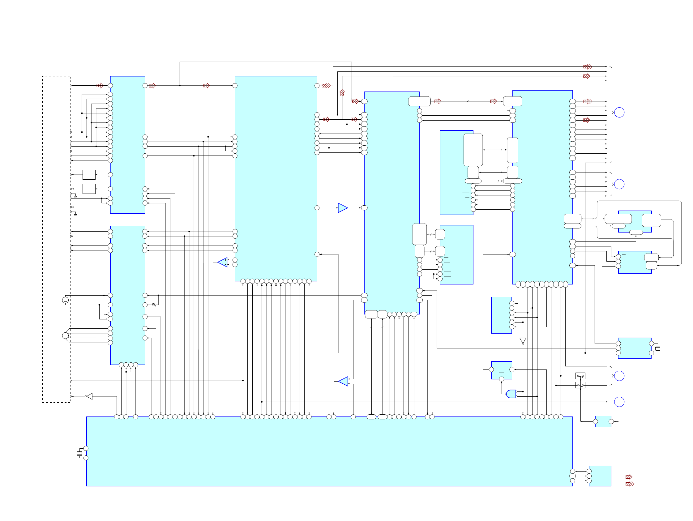
HCD-GX90D/RV800D
– DVD SYS Section –
MAIN
SECTION
(Page 24)
S1002-1014
FUNCTION
KEY
S1022-1034
FUNCTION
KEY
S1042-1055
FUNCTION
KEY
S1081
ENCODER
VOLUME
F
HP
X1101
5MHz
IC1001
DISPLAY CONTROL
22 KEY0
KEY1
21
20 KEY2
13 VOL1A
14 VOL1B
3X1
4X2
17
HEADPHONE
ENTER
SEG1-33
26
27GAME-MIXING
28GAME-LED
29MD/VIDEO
30TAPE
31TUNER
32CD/DVD
16DECODE-LED
9S-OUT
8S-IN
7S-CLK
6RESET
33-58
61-67
68-80G1-13
Q1004-1008
Q1010-1012
LED
DRIVER
Q1001-1003
GRID
DRIVER
D1001-1005
D1007-1009
FL1001
FLUORESCENT
INDICATOR
TUBE
DVD DSP
SECTION
(Page 21)
IC1002
1110
56
34
IR
S1062
DISPLAY
S1061
POWER
REMOTE
CONTROL
RECIEVER
C
1312
98
12
IC1003
I2C-CL
I2C-DA
SYS-RESET
X800
32.768kHz
X801
16MHz
IC1104(3/3)
MASTER CONTROL
73 DISPLAY KEY
74 3POWER KEY POWER
CD/DVD POWER
4 SIRCS
29 IIC-CLK
30 IIC-DATA
41 SYS-RESET
S-IN
100
S-OUT
1
S-CLK
2
M-RESET
42
10 XC-IN
11 XC-OUT
13 X-OUT
15 X-IN
Q1009
LED
DRIVER
34
40SYS-POWER
40STB-RELAY
12RESET
18ACCUT
RESET
SWITCH
Q714
Q706
D1006
POWER
D+5V
(DVD)
+5V
DVD+12V
GC+5V
IC704
REG
IC706
REG
IC703
RESET
M+9V
A+12V
D+4V
IC921
REG
12
4
AC3
AC4
IC901
REG
Q901
RELAY
DRIVE
F914
F915
F916
F917
F918
F919
VF
D902-905
13
IC922
REG
13
IC923
REG
13
IC934
REG
13
IC932
REG
13
Q723-725
SWITCH
13
Q715-716
SWITCH
13
IC705
REG
1
5
Q717
13
UNREG+20V
VP
UNREG+12V
+VH
-VH
+VL
-VL
Q971
REG
EVER+4V
D271
D371
D732
D911
D733
T911
POWER TRANSFORMER
T901
SUB TRANSFORMER
F913
RY901
AC
IN
2222
Page 23
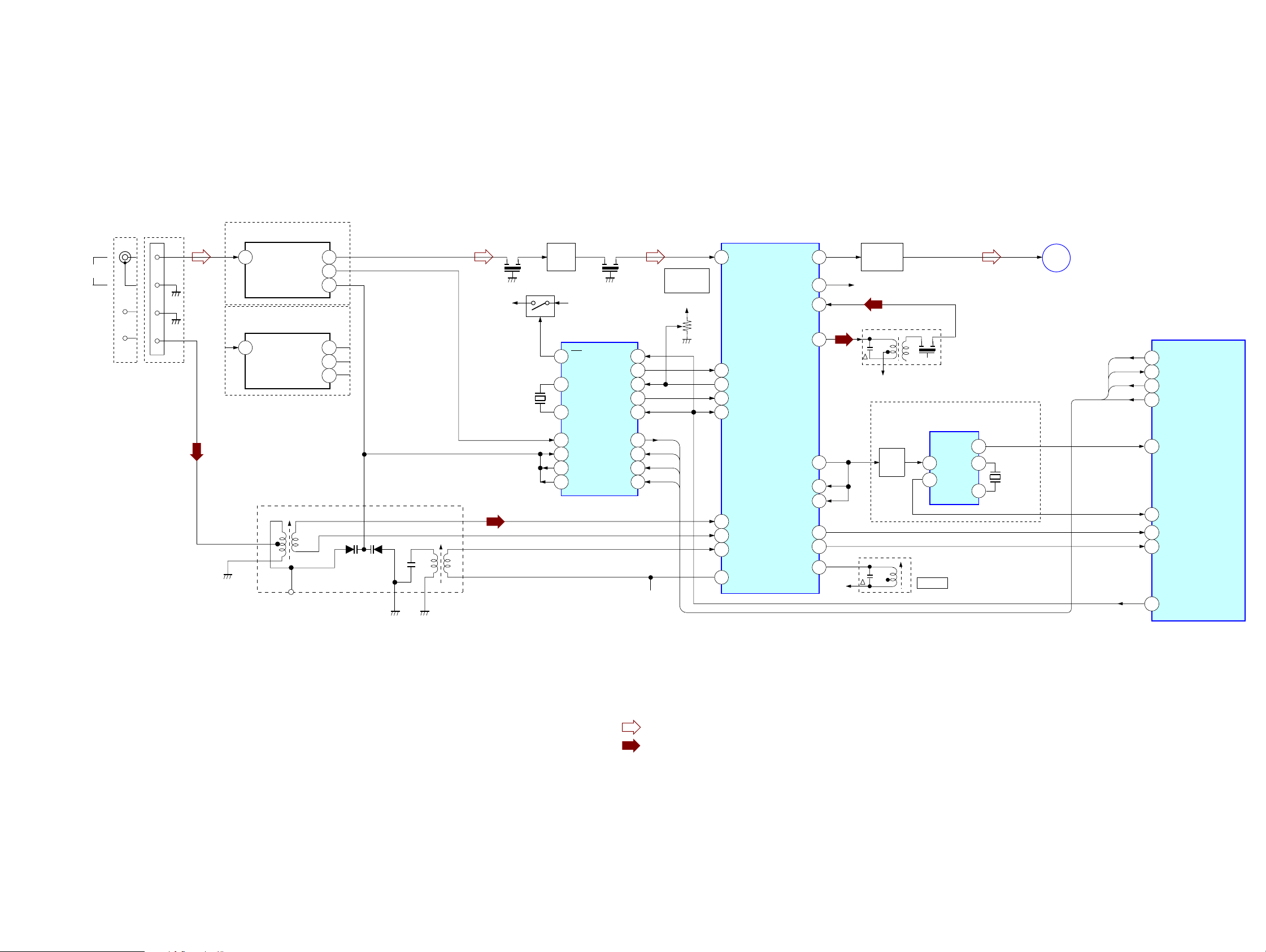
– Tuner Section –
TM1
TM1
(AEP, UK)
FM 75Ω
G
AM
( EXCEPT AEP,UK)
FE3(AEP,UK)
1
ANT IN
OSC OUT
FE2
(EXCEPT AEP,UK)
8
ANT IN
2
11
49
IF OUT
IF OUT
F OUT
VT
VT
7
8
5
1
3
4
RB41
10
HCD-GX90D/RV800D
AM/FM IF MPX
Q1
CF1 CF2
+B
(FE2,3)
X51
4.5MHz
1
3
8
7
6
Q2
RF IF
AMP
10
1
22
16
20
19
18
A+12V
FM
XIN
XOUT
FM OSC
AOUT
AIN
PD
PLL
IC51
IF IN
AM OSC
FM
CL
CE
12
7
15
9VCO STOP
8IF REQ
6DO
4DI
5
3
A+12V
1
FM TUNED
LEVEL
A+12V
RV11
11
24
12
10
DO
DI
CL
CE
21
22
23
9
IC11
FM IF
AM MIX OUT
AM/FM
OSC FM
VCO STOP
IF REQ MUTE
DECORDER
PLL IN OUT
DECORDER
AM RF IN
AFC
AM OSC
VCC
L OUT
R OUT
AM IF IN
IN
TUNED
STEREO
FM-DET
13
14
4
2
18
17
16
6
7
8
A+12V
R-CH
AMP
Q11
A+12V
AMP
Q81
IFT11
T11
4
2
NULL
IC81
DECODER
INT
DATA
16
13
14
L-CH
AEP,UK
X801
4.332MHz
E
MAIN
SECTION
(Page 24)
DI
DO
CL
CE
MASTER CONTROL
IC1104(1/3)
26
ST-DOUT
27
ST-DIN
28
ST-CLK
ST-CE
25
20
RDS-INT
21
RDS-DATA
TUNED
24
STEREO
23
22
ST MUTE
• RCH is omitted due to same as LCH
• Signal Path
: FM
: AM
2323
Page 24
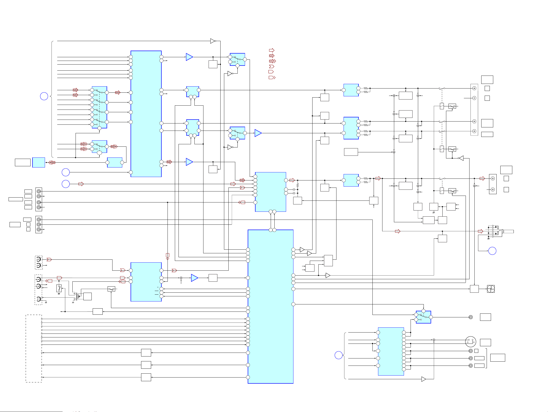
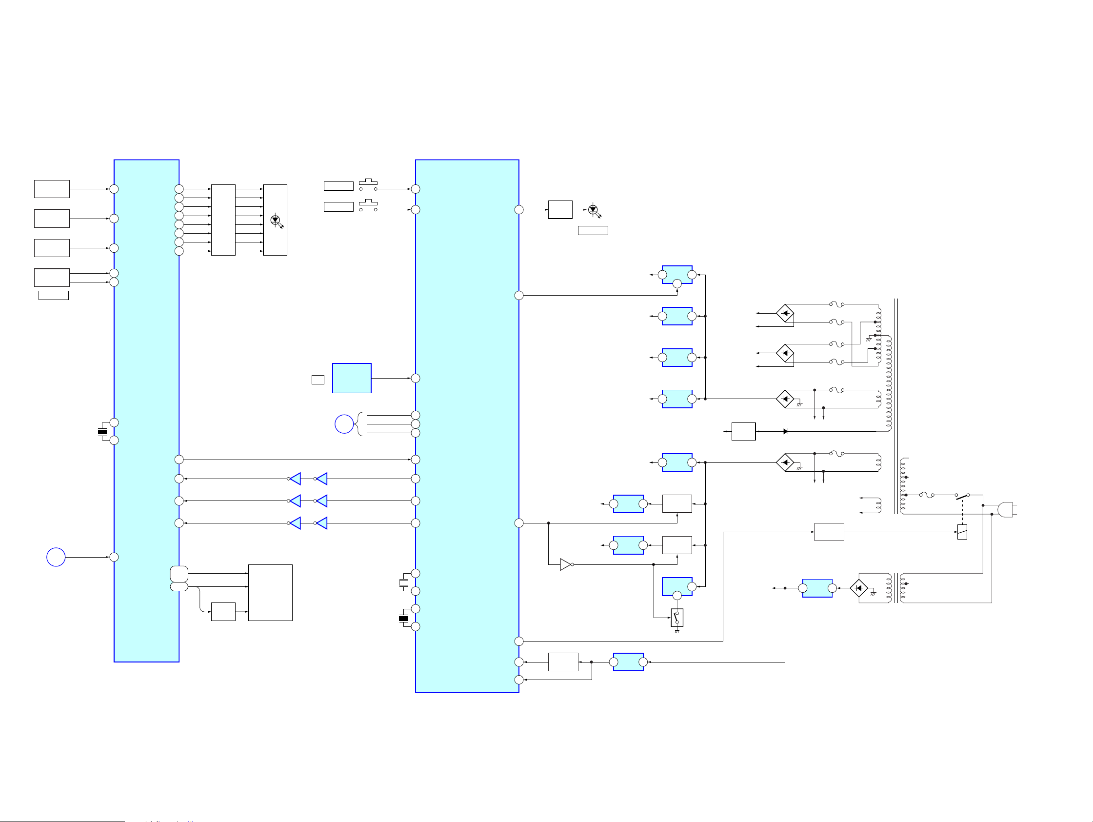
HCD-GX90D/RV800D
– Main Section –
DIGITAL OUT
OPTICAL
VIDEO(MD)
INPUT
IN L
IN R
OUT L
OUT R
VIDEO
REC/PB
HEAD
ERASE
HEAD
L
R
HEAD
DVD DSP
SECTION
(Page 21)
IC501
OPTICAL
DIGITAL
J1001
DECK-A
PB
DECK-B
TC BLOCK
B SHUT
A SHUT
B PLAY
A PLAY
B HALF
A HALF
B REC REV
B REC FWD
CAP M+
A TRG M+
OUT
J101
MREQ
IC302
D/A CONVERTER
MDI
MC
ML
DATA1
DATA2
DATA3
IC305
TUNER
T601
DIGITAL AUDIO SELECTOR
13
14
10
11
OPTICAL OUT SELECTOR
12
Q601
BIAS
OSC
3
2
6
5
IC303
5
Q608,609
SWITCH
12
4
9
7
1
8
1,2
4 TIMING
Q602,603
IC504
DATA0
R-CH
R-CH
R-CH
DVD DSP
SECTION
(Page 21)
TUNER
SECTION
(Page 23)
R-CH
R-CH
Q604
Q605
R-CH
PCMD
BCK-ZIBA
BCK
LRCK-ZIBA
LRCK
XCK
768FS
IEC958
DOUT
CDSEL
D
E
XRSTCD
A
TC12V
1
34 MDI
35 MC
36 ML
45 DATA1
46 DATA2
47 DATA3
DATA4
31
BCK
40
41
LRCK
38
SCKI
37 RST
REC/PB AMP
32 A-IN(L)
34 B-IN(L)
21 REC-OUT(L)
Q615,616
CAP M
DRIVE
Q617,618
B TRIG
DRIVE
Q613,614
A TRIG
DRIVE
IC601
14VOUT1
13VOUT2
RCH
12 1
11VOUT4
RCH
10VOUT5
9VOUT6
16VOUT7
20VOUT8
RCH
26PB-OUT(L)
28EQ-OUT(L)
24REC-IN(L)
13A/B
14MUTE ON/OFF
15REC.MUTE OFF/ON
R-CH
IC506
BUFFER
IC510
EVR
4 5
IC509
EVR
1
8 7
4 5
IC505
BUFFER
IC303
AMS AMP
Q110
IC105
SWITCH
4
3
Q107
Q106
2
10
11
15
10
IC104
SWITCH
13
DVD
TUNER
TC
LINE
GAME
IC1104(2/3)
MASTER CONTORL
56
SURR-SW
31 VOL-CLK
33 VOL-DATA2
32 VOL-DATA1
72 AMS-IN
76
PB-A/B
78
PB-MUTE
79
REC-MUTE
75 BAIS
77 TC-RELAY
B-SHUT81
A-SHUT
80
B-PLAY71
70
A-PLAY
69
B-HALF
68
A-HALF
B-REC.REV
67
B-REC.FWD
66
65
CAP M-CONT
61
B-TRIGB TRG M+
60
A-TRIG
MUTE
Q106
2VOUT3
2
MUTE
Q108
Q610,611
AMS
DET
• RCH is omitted due to same as LCH
• Signal Path
IC101
BUFFER
IC102
SOUND CONTROLLER
42 SUR1
3 INA1
4 INB1
5 INC1
6 IND1
7 INEX1
8RECB1
DATA
21 22
5 7
M61519-DATA
: FM
: DVD
: DIGITAL OUT
: PB(DECK A)
: PB(DECK B)
: REC(DECK B)
18LOUT
17
BBB1
16
BBA1
CLOCK
REAR/CEN
M61519-CLOCK
MUTE
IC300
POWER AMP
10
15
11
MUTE
Q155
Q154
MUTE
Q104
MUTE
Q103
MUTE
DBFB
SW
Q101
Q719
Q721
52
51SW-MUTE
83LINE-MUTE
D734,735
AC4
84STK-MUTE
87REAR-RELAY
88FRONT-RELAY
50FNN
55VIDEO-SW
DET
Q702,703,707
LINE
AC
MUTE
Q701
DVD DSP
SECTION
(Page 21)
POWER AMP
1
15
TH301,Q316,317
OVERHEAT
POWER AMP
15
B
IC302
DET
IC201
V
C
Y
CB/R
CR/B
WIDE
6
7
10
11
10
11
DBFB
DET
RCH
4 V-IN
2 C-IN
6 Y-IN
12 CY-IN
14
CB-IN
16
CR-IN
RCH
RCH
IC503
VIDEO BUFFER
V-OUT.B
C-OUT
Y-OUT.B
CY-OUT.B 25
CB-OUT.B 22
CR-OUT.B 19
Q351
OVERLOAD
DET
Q341
OVERLOAD
DET
Q441
OVERLOAD
DET
Q251
OVERLOAD
DET
30V-OUT.A
31
33
27Y-OUT.A
28
24CY-OUT.A
21CB-OUT.A
18CR-OUT.A
Q236,237
VIDEO SELECTOR
DC
DET
1
3
Q501,502
RCH
RCH
Q233,234
PROTECT
2
IC502
Q235
DET
RELAY
SW
7
RY381
RY382
RY281
MUTE
HP
MUTE
D230,231
Q232
Q152
Q381
Q382
Q281,282
AC
DET
RCH
+VL
+VL
Q384
+VH
AC3
C
Y
TM400
FAN
SW
RCH
RCH
R CH
Q713,
Q708-710
S VIDEO
Y
PB/C
B
PR/C
R
REAR
SPEAKER
L
R
CENTER
SPEAKER
WOOFER
HP
J503
VIDEO
OUT
J502
OUT
TM201
F
FAN
J501
COMPONENT
VIDEO OUT
FRONT
SPEAKER
DVD SYS
SECTION
(Page 22)
L
R
J1101
PHONES
2424
Page 25
6-2. Circuit Boards Location
HCD-GX90D/RV800D
THIS NOTE IS COMMON FOR PRINTED WIRING BOARDS AND SCHEMATIC DIAGRAMS.
(In addition to this, the necessary note is printed in each b lock.)
SUB TRANSFORMER board
TRANSFORMER board
PANEL board
REMOTE board
SUB PANEL board
SENSOR board
DIODE board
MOTOR board
TC board
DRIVER board
RF board
MAIN board
MB board
Note on Schematic Diagram:
• All capacitors are in µF unless otherwise noted. pF: µµF
50 WV or less are not indicated except for electrolytics
and tantalums.
• All resistors are in Ω and 1/
specified.
f
•
• 5 : fusible resistor.
• C : panel designation.
• A : B+ Line.
• B : B– Line.
• H : adjustment for repair.
•Voltages and waveforms are dc with respect to ground
•Voltages are taken with a VOM (Input impedance 10 MΩ).
•Waveforms are taken with a oscilloscope.
• Circled numbers refer to waveforms.
• Signal path.
•Abbreviation
: internal component.
Note:
The components identified by mark 0 or dotted
line with mark 0 are critical for safety.
Replace only with part
number specified.
under no-signal (detuned) conditions.
Voltage variations may be noted due to normal produc-
tion tolerances.
Voltage variations may be noted due to normal production tolerances.
F : FM
f : AM
E : PB (DECK A)
d : PB (DECK B)
G : REC (DECK B)
c : digital out
g : MD (VIDEO)
CND : Canadian model
4
W or less unless otherwise
Note:
Les composants identifiés par
une marque 0 sont critiques
pour la sécurité.
Ne les remplacer que par une
piéce portant le numéro
spécifié.
Note on Printed Wiring Boards:
• X : parts extracted from the component side.
• : Pattern from the side which enables seeing.
• Indication of transistor.
C
B
B
Q
E
CE
These are omitted.
These are omitted.
REG board
VIDEO board
SURROUND board
FRONT AMP board
2525
Page 26
HCD-GX90D/RV800D
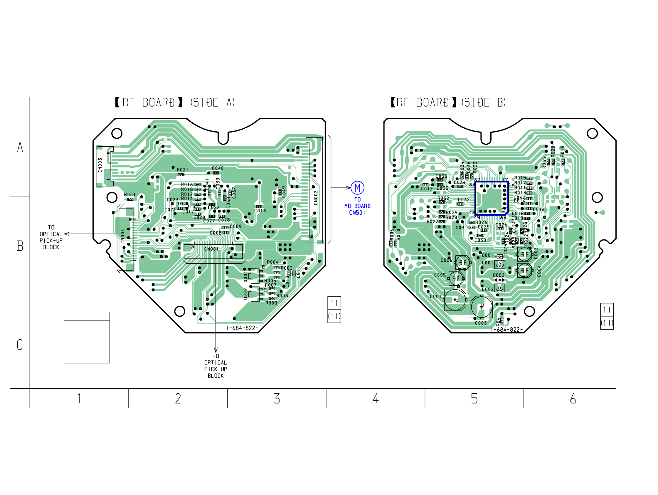
6-3. Printed Wiring Board – RF Board –
• See page 25 for Circuit Boards Location.
• Semiconductor
Location
Ref. No. Location
D001 B-5
D002 B-5
IC001 A-5
Q001 C-3
Q002 C-3
IC001
(Page 28)
2626
Page 27
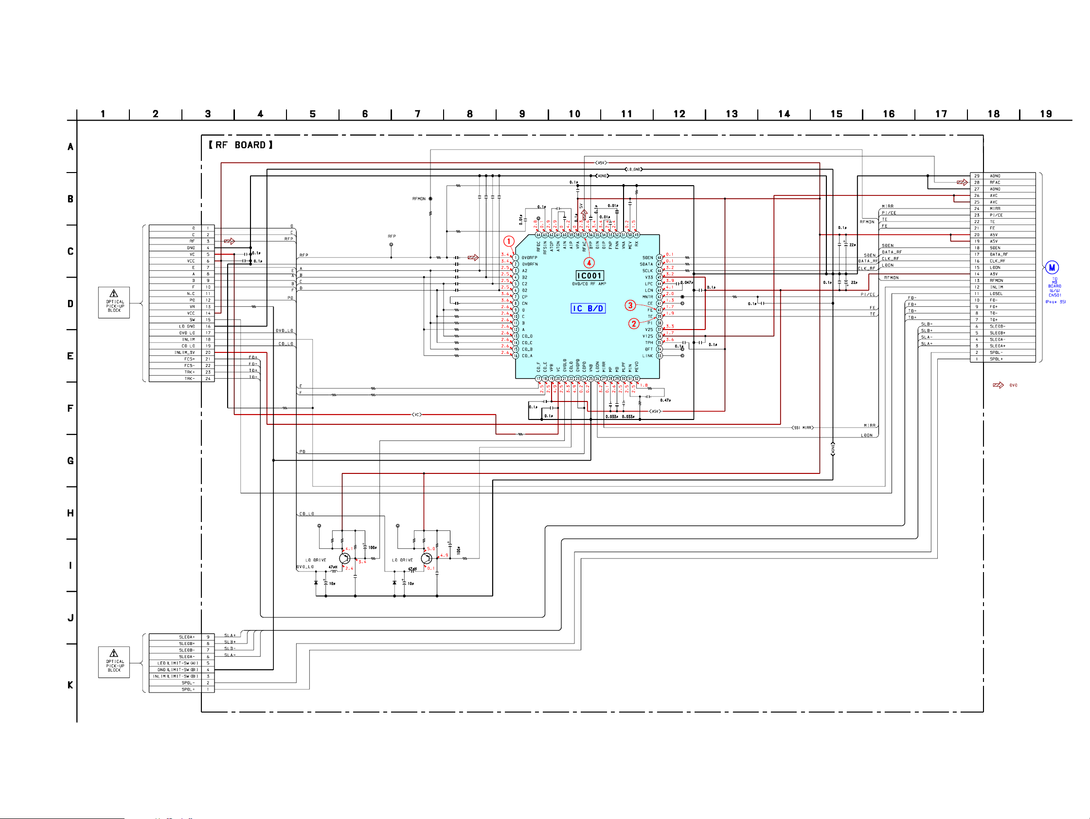
HCD-GX90D/RV800D
6-4. Schematic Diagram – RF Board –
CN001
24P
• See page 55 for Wavefoms. • See page 64 for IC Block Diagrams.
R023
JL005
C008
B
C009
B
R001
100 E
JL007
820
CH
R024
0
5600p B
5600p B
2200p B
2200p B
2200p B
2200p B
180p CH
0
0
0
0
0
0
0
0
22p
C020
R025
100
C019
C018
220
R022
C017
C016
C015
C014
C042
R014
R013
R012
R011
R018
R017
R016
R015
CN002
29P
C027
B
CH
CH
CH
22p
22p
22p
C023
C022
C021
C025
B
B
JL004
C024
B
C028
B
C026
IC001
CXD1881AR
C031
R026
1000p
12k
CH
C030
C029
B
E
B
C013
B
C006
R027
0
R028
0
R029
0
C032
C033
B
JL006
JL003
C034
B
JL002
JL001
B
C049
R032
100
B
C035
B
10V
C005
C012
10V
B
CN003
0
R035
00
R041
1k
9P
R019 R020
R005
47k
33
R003
Q001 Q002
2SB1132-T100-QR 2SB1132-T100-QR
L001
C010
1000p
C002 C004
D001 D002
1SS355TE-17 1SS355TE-17
CH
16V 16V
IOP1IOP2
C001
6.3V
R006
470
C041
B
C040
B
R021
0
R009
47k
33
R008R004
3333
R007
L002
1000p
6.3V
C003
R010
470
C011
CH
C039 C038
R033
0
B
C036
C037
R034
330p
10M
CH
2727
Page 28
HCD-GX90D/RV800D
6-5. Printed Wiring Board – MB Board (Side A) –
• See page 25 for Circuit Boards Location.
CN501
IC701
IC215
IC206
(Page 26)
IC904
IC902
IC906
TH
EXCEPT
TH
IC509
• Semiconductor
Location
Ref. No. Location
D301 E-3
IC901
X902
D302 E-3
IC206 C-1
IC215 C-2
IC302 E-3
IC303 D-2
IC509 B-4
IC701 B-1
IC901 C-3
IC902 C-3
IC904 C-3
IC906 D-3
Q903 E-4
Q904 E-4
IC303
(Page 42)
(Page 38)
IC302
(Page 38)
(Page 42)
2828
Page 29
HCD-GX90D/RV800D
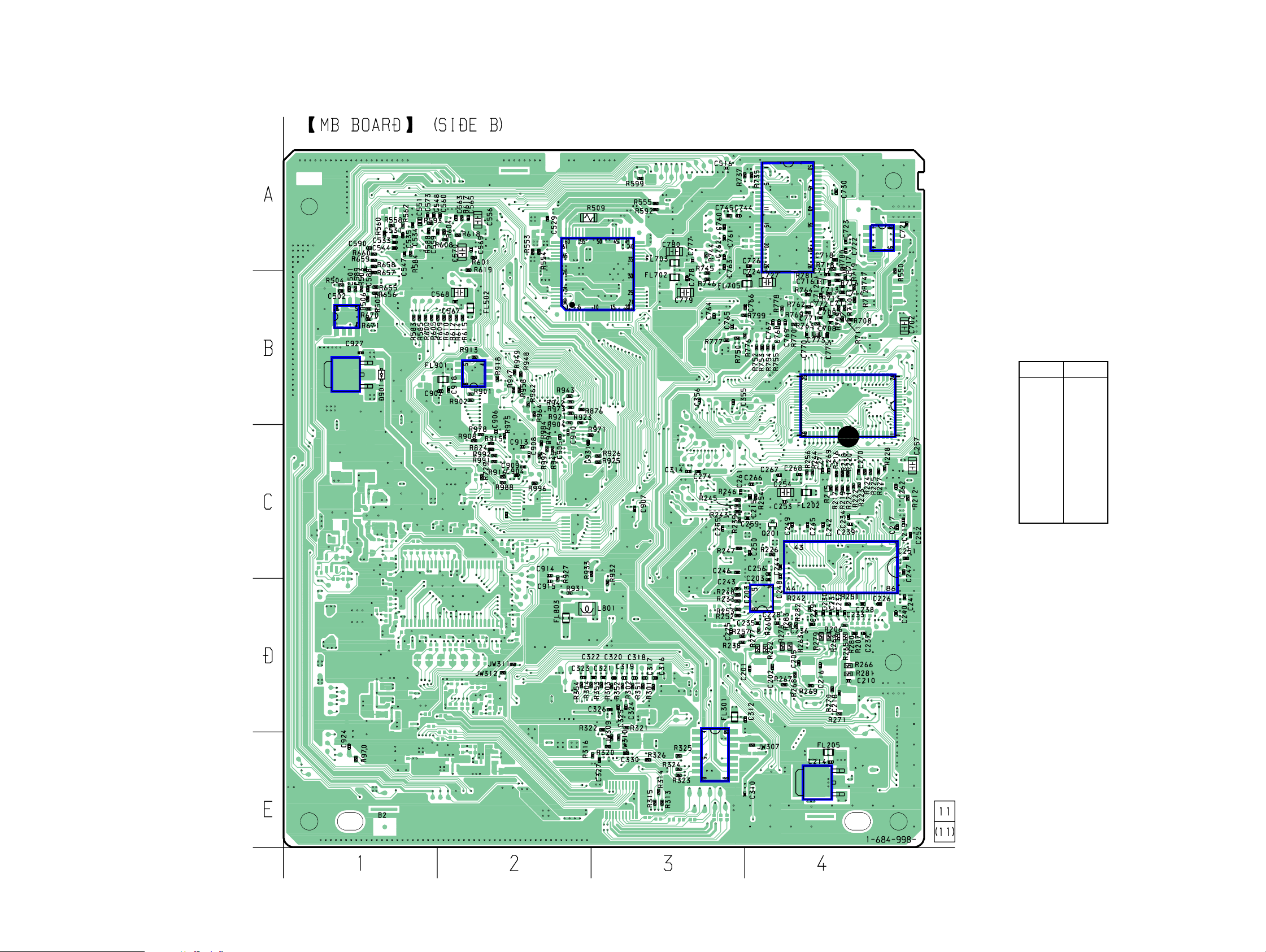
6-6. Printed Wiring Board – MB Board (Side B) –
IC503
• See page 25 for Circuit Boards Location.
IC907
IC903
IC706
IC703
IC501
• Semiconductor
Location
Ref. No. Location
D901 B-1
TH
IC203
IC205
IC202
IC202 C-4
IC203 D-4
IC205 B-4
IC210 E-4
IC305 E-3
IC501 B-3
IC503 B-1
IC703 A-4
IC706 A-4
IC903 B-2
IC907 B-1
2929
IC305
IC210
Page 30

HCD-GX90D/RV800D
6-7. Schematic Diagram – MB Board (1/6) –
• See page 58 for IC Pin Function Description.
IC703(2/2)
NJM3404AM-TE2
R544
100k
C523
1500p
FL706
POWER-EMIS
FL704
POWER-EMIS
R767
47k
C774
R765
0.0047
22k
B
C729
10 10V
R702
0
FL703
POWER-EMIS
B
R799
0
C781
100 4V
R764
C771
0.047
R545
B
C780 C777
R755
0
100k
R540
10k
R541
100k
R538C521
100k1500p B
R701
0
10
0.1
10V
F
POWER-EMIS
C776
0.1 F
SL703
C772
0.1 F
1M
C773
0.47
B
R762
R759
0
R758
0
R757
0
R756
R766
0
R763
8.2k
CL791
R777
R550
0
B
C701
C705
100
0.01
4V
FL701
POWER-EMIS
FL702
C779
10 10V
R769
2.2k
22k
0
R754
0
R753
0
R752
0
C766
100p
R750
10k
0
C778
0.1
F
C775
0.1
F
C770
0.1
F
R770
0
C769
0.1
F
R778
100k
C768
0.1
F
C767
0.1
F
CL787
CL786
CL785
R776
CH
C765
0.1
0
F
TP701
ER-EMIS
TP703
C715
R700
0.0015
8.2k
B
R725
1.8k
R724
1k
IC703(1/2)
C703
0.1
B
C706
C702
R707
0.1
10
100
F
10V
B
C709
0.01
470k
0.1
F
C708
R708
R709
150k
C711
0.01 B
C712
100p
CH
R712
R710
10k
R711
2.2k
10k
10k
R713
CL703
C752
0.1
R714
10k
NJM3404AM-TE2
R781
F
F
0.1
0.1
33k
C714
C713
10k
R747
R715
R721
R720
0
R716
33k
R748
33k
1k
C717
B
0.01 B
CL701
R718
10k
0.47
F
0
C716
100k
0.1
R780
100
R717
C718
1k
R719
IC701
CXD1882R
R726
C720 C721
0.1 B 0.1 F
100k
F
0.1
C722
FL705
POW
B
R727
3.3k
C727
0.1
10
R728
10k
F
0.1
C723
C724
10V
C728
0.1 F
IC706
MSM51V18165F -60TSKR1
C725 C726
0.1 F 0.1 F
C730
0.1 F
R730
22
C740
R731
0.1 F
22
C741
0.1 F
R732
10k
C742
0.1 F
R771
10k
R773
10k
C743
0.1 F
R735
10k
R774
10k
R737
10k
R779
10k
R784
10k
0.1 F
C744
22
R741
R742
22
C745
0.1 F
R743
22
CL777
22
R744
0.1
F
C763C764
0.1
F
R746
C762
0.1
F
R745
47k
47k
C761
C760
0.1
0.1
F
F
3030
Page 31

HCD-GX90D/RV800D
6-8. Schematic Diagram – MB Board (2/6) –
C793
220
4V
C791
100
6.3V
JL901
JL906
JL907
JL902
CN905
11P
JL903
JL904
JL905
JL920
• See page 61 for IC Pin Function Description. • See page 55 for Wavefoms.
FL901
POWER-EMIS
C901
IC907
C926
220
4V
2SK1828TE85L
IC903
BR24C08F-E2
C927
0.01
F
Q904
R913
10k
C918
0.01
F
Q903
2SK1828TE85L
100 4V
C902
0.01
F
R958
22
22
R918
0
R919
0
R949
0
R948
0
D901
1SS355TE
C925
22
16V
R970
0
F
C924
0.01
R947
R962
CL969
CL968
10k
R964
10k
22
R901
22
R902
R943
0
0
0
100
100
100
R876
R973
R910
R942
R921
100
R940
C906
0.01 F
IC901
CXP973064-224R
C910
0.01
F
X901
20MHz
10k
R978
0
R971
R729
0
R805
0
22
22
22
2.2k
R906
R905
R907
2.2k
R912
R911
F
0.01
100
100
C905
R930
R929
R904
10k
100
100
100
R926
R925
R928
R935
4.7k
Q901
DTC114TE-TL
JL956
JL958
JL957
CL934
IC906
IC902
TC7S32FU
0
R991
CL924
0
R992
100
R915
0
R824
C904
C903
100
0.01
C909
4V
F
100p
0
R988
R994
0
R995
0
0
R996
R997
0
R998
R920
100
R990
0
R922
22
R944
10k
R945
10k
R923
220
FL908
POWER-EMIS
R916
1k
C908
100p
R917
1k
C913
33000p
B
0
R984
10k
R908
10k
R975
10k
TE85L
IC904
TC7W74FU
(TE12R)
CL801
R931
47
C915
9p
X902
C914
27MHz
9p
100 4V
C916
C907
0.01
C917
0.01
F
L801
F
FL803
POWER-EMIS
SM8707GV-G-E2
R932
47
CL825
R933
47
R927
1M
CN901
JL954
JL959
JL955
JL950
JL951
JL952
JL953
7P
JL922
JL923
JL921
JL924
CN906
13P
3131
Page 32

HCD-GX90D/RV800D
6-9. Schematic Diagram – MB Board (3/6) –
CN202
17P
JL209
JL208
R267
JL212
4.7k
4.7k
4.7k
R250
0
R258
R232
R238
0
100
CL348
R259
CL347
4.7k
R260
R257
C235
0.01
F
CL343
CL345
CL346
CL342
CL341
C225
C228
0.1
0.01
F
F
CL340
CL338
0
C201
0
R277
75
R262
75
C236
0.01
R283
F
180
1k
R282
0
R272
0
R206
JL207
R268
0
R269
0
C202
C205
0
0
R279
R278
75
75
R264
R263
75
75
C230 C231 C232 C233
C229
0.01F0.01F0.01F0.01
0.01
F
0
0
R274
R273
JL206
R270
0
R271
0
C216
0
R265
75
0
R275
JL205
C218
0
JL204
R281R280
7575
R266
75
C237
0.01
F
0
R276
F
CL322
CL323
CL324
CL208
JL203
JL202
JL201
JL210
JL211
Q201
DTC114TE-TL
R253
4.7k
R252
4.7k
R233
R239
47k
C246
0.01
F
R242
0
C250
0.01
IC203
BR9040F
C203
0.01 F
C256 C259
0.01
F
F
R240
0
C255
0.01
F
R254
0
10k
R248
4.7k
C243
0.01
F
IC206
R226
4.7k
R247
4.7k
0.01
F
R245
10k
C215
0.01
F
C261
0.01
F
ZIVA-5P-BO
C240
0.01
F
C241
0.01
F
C247
0.01
F
C251
0.01 F
C252
0.01
F
C260
0.01
F
R212
22
C262
0.01
F
FL204
33
33
33
33
C264
D201
1SS355TE
IC210
FL205
C212C213
C214
0.01
F
100
0.01
4V
F
10
10V
C265
0.01
F
R229
R230
33
C266
0.01
F
C267
0.01
33
R231
33
F
4.7k
R244
4.7k
R256
C268
0.01
F
C271
0.01
F
33
33
33
R215
R217
R216
R218
C269 C270
0.01
F
33
33
33
R219
R220
R222
R221
33
R224
R223
R225
0.01
F
R228
R227
33
33
3232
Page 33

6-10.Schematic Diagram – MB Board (4/6) –
HCD-GX90D/RV800D
IC202
MT48LC4M32B2-7
C217
0.01
F
C219
0.01
F
C226
0.01
F
C234
0.01
F
C238
0.01
C239
0.01
F
F
R251
10k
C242
0.01
F
C244
0.01
F
C245
0.01
F
C248
0.01
F
C249
0.01
F
C253
C254
FL202
C314
C274
0.01
F
9
0
4
5
3
3
L
L
C
C
0.01
F 0.01
1
5
3
L
C
4
2
3
5
5
3
3
L
L
C
C
7
5
6
5
5
5
5
3
3
3
3
L
L
L
L
C
C
C
C
8
0
9
5
6
5
3
3
3
L
L
L
C
C
C
IC215
SN74ALVCH16841
DGGR
2
1
6
6
3
3
L
L
C
C
C315
F
3
4
5
6
6
6
3
3
3
L
L
L
C
C
C
8
7
6
6
3
L
C
9
6
6
6
3
3
3
L
L
L
C
C
C
0.01
10
10V
F
FL203
C257
C258
10
0.01
10V
F
IC205
R213
0
C263
R261
0
R249
0
R214
0
0.01
C204
0.01 F
F
1
2
3
8
9
8
8
3
3
L
L
C
C
5
6
8
8
8
8
8
3
3
3
3
3
L
L
L
L
L
C
C
C
C
C
C356
0.01
F
4
7
8
0
9
8
8
7
8
3
3
3
3
37
L
L
L
L
L
C
C
C
C
C
4
5
7
6
7
7
7
7
3
3
3
3
L
L
L
L
C
C
C
C
C355
0.01
F
1
3
2
0
7
7
3
37
37
L
L
L
L3
C
C
C
C
3333
Page 34

HCD-GX90D/RV800D
6-11.Schematic Diagram – MB Board (5/6) –
CN302
23P
JL301
JL302
JL303
JL304
JL305
JL306
JL307
JL308
JL309
JL310
JL311
JL312
JL313
• See page 63 for IC Block Diagrams.
FL302
C302
0.01
F
C303
10
16V
D302
1SS355TE
R307
10
1SS355TE
C316
R301
100p
220
CH
R351
C317
220
100p
CH
R302
C318
0.01
220
B
C319
R352
0.01
220
B
C320
R303
0.01
220
B
R353
C321
0.01
220
B
R304
C322
0.01
220
B
R354
C323
0.01
220
B
JW303
FL303
C308
D301
0.01
F
C307
100
6.3V
0
304
0
JW
JW312
0
100p
C310
IC303
SN74HC00ANSR
R326
22
100
R315
R313
100
100
R314
JW307
C324
0.1
16V
F
C325
0.1
16V
F
C327
0.1
16V
F
R320
22
R321
22
R322
22
SL301
SL302
IC302
PCM1608
C326
0.1
C328
100
6.3V
FL301
C311
0.1
F
C312
100p
CH
IC305
SN74HC157ANSR
0
R323R324
2222
22
R325
JW309
0
CN304
2P
3434
Page 35

HCD-GX90D/RV800D
6-12.Schematic Diagram – MB Board (6/6) –
CN501
29P TO RFAMP
TP511
TP512
TP509
TP510
JL500
JL544
JL537
JL536
JL535
JL531
JL530
JL529
JL527
JL526
JL525
JL524
JL523
JL522
JL501
JL502
JL511
JL512
JL509
JL510
JL503
JL504
JL505
JL506
JL507
JL508
• See page 63 for IC Block Diagrams.
C592
10
16V
R592
0
C516
0.0022
R599
1k
R555
0
JL547
CL505
MNT0
CL504
MNT1
CL503
MNT2
CL502
MNT3
CL501
GND
0
0
R583
C522
0.1 B
R536
R537
10k
68k
F
10V
10
0.01
C517
C518
IC503
NJM3404AM-TE2
C502
0.01
C501
0.01
R504
R503
47k
47k
R505
47k
R506
47k
R507
0
SL501
SL502
R561
R560
1k
R558
47k
1k
R569
0
10k
R670
10k
R671
C545
10 10V
C543
0.1 F
1k
R655
C588
0.0022 B
C589
0.0022 B
B
B
C533
0.047
0.0022
C531
R562
1k
C534
0.022
B
0.0022
0.0022
1k
R656
1k
R657
1k
R658
1k
R659
1k
R660
C590
B
R578
0
R577
0
C544
C535
0.1
B
B
R585
IC509
CXD3068Q
10k
33k
R593
100k
R588
R584
C548
0.01
B
C547
0.1
F
C551 C573
0.47B100p
CH
B
0.0033
C553
C560
0.0015 B
R587
0
0
0
0
0
0
0
R600
R605
1k
R604
0
R614
R615
R609
R610
R612
C565
10k
R608
0.1
B
B
CH
C559
0.1
1M
R603
100p
3.3k
R613
C563
C558
C556
C561
100
10
0.1
4V
10V
FL502
PWR-EMIS
C567
0.1
F
C568
10V
10
R630
10k
0
R623
0
R622
CL508
CL507
CL506
R629
0
R619
0
R618
470k
R617
1M
FL501
PWR-EMIS
F
0
R628
0
R627
0
R626
330
R625
C570
10
R601
10V
10k
C569
0.1
F
R543
R547
0
JL521
C526
22
16V
C527
0.01 F
R509
0
C529
0.01 F
C528
22 16V
R597
0
R510
150k
R511
150k
0
0
R553
R554
IC501
FAN8035L
C525
0.01
F
R580
33k
10k
R589
B
C504
33000p
R513
56k
C503
33000p B
R581
C519
0.01
B
R512
56k
0
12k
R579
8.2k
C514
R533
0.01
33k
B
R532
0
C512
R529
0.01
33k
B
R528
0
C510
0.001
B
R527
2.2k
R522
4.7k
C509
330p
B
R586
200k
C506
330p
R516
4.7k
B
R535
R534
0
56k
R531
R530
0
56k
R525
10k
R524
10k
R521
100k
R523
10k
R519
100k
R520
10k
C508
0.001
R517
2.2k
B
3535
Page 36

HCD-GX90D/RV800D
6-13.Printed Wiring Board – TC Board –
• See page 25 for Circuit Boards Location.
IC601
• Semiconductor
Location
Ref. No. Location
IC303 C-3
IC601 B-2
Q601 D-2
Q602 D-2
Q603 D-2
Q604 C-2
Q605 C-2
Q606 C-2
Q607 C-2
Q608 C-3
Q609 D-3
Q610 C-4
Q611 C-4
IC303
(Page 38)
(Page 38)
3636
Page 37

6-14.Schematic Diagram – TC Board –
C628
680p
C662
0.01
C625
2.2
R630
R629
50V
5.6k
5.6k
C624
2.2
50V
C657
2.2 50V
R626
R627
1k
50V
C623
2.2
HCD-GX90D/RV800D
10k
C622
0.0015
C620C621
2.2 50V1
50V
R624
C619
0
4700p
R623
2.2k
R622
22k
C617
2.2 50V
C618
R621
0.0022
12k
CN602
CN603
8P
SAN
SAN
R636
C637
1 50V
R659
4.7k
27k
C627
C636
0.015
C626
47 16V
C630
16V
Q604
2SC2785
47
Q605
R658
4.7k
2SC2785
T601
R637
560
C601
0.01
C602
R601
R602
2.2
5.6k
5.6k
50V
HA12237F
C638
0.022
Q603
2SC2785
IC601
C603
2.2
50V
2SB1116
Q602
C604
R604
1k
50V
2.2
R605
R638
R620
22k
C609
2.2 50V
R610
R692
C608
R608
10k
C658
4700p
0
16V
100
R689
R609
22k
2.2k
1k
R662
1k
R663
C605
50V
10k
10k
1
R691
C607
2.2 50V
C606
0.0015
C656
2.2 50V
Q608
2SB1116
10k
10k
R660
Q609
2SC2785
C655
4.7 50V
R639
4.7k
R606
4.7k
C615
100
16V
R618
220
R617
4.7k
R616
4.7k
R615
4.7k
50V
25V
47k
R612
C611
22
R611
12k
C610
10k
10k
R631
C659
100
16V
C612
10
0.0022
C660
R613
25V
47k
R614
C613
22
R661
100
IC303(2/2)
NJM4565M(TE2)
R664
1M
22p
47k
C661 C663
0.1 0.1
R665
10k
R666
10k
JW651
IC303(1/2)
NJM4565M(TE2)
C664
50V
10
R667
CN608
7P
CN609
7P
22k
R669
C665
16V
47
Q611
BA1L3Z
22k
R670
Q610
2SC2785
R668
4.7k
10k
680p
C629
3P
C632
680p
Q606
2SC2785
C631
680p
Q607
2SC2785
Q601
2SC2001
C633
0.0047
C635
0.015
47 16V
3737
Page 38

HCD-GX90D/RV800D
6-15.Printed Wiring Board – Main Section –
A
B
IC1104
C
(Page 48)
D
• See page 25 for Circuit Boards Location.
(Page 42)
(Page 42)
IC105
(Page 51)
IC703
(Page 28)
(Page 28)
IC51
IC11
RV800D
IC81
E
IC705
IC102
IC706
F
IC704
G
IC101
IC104
H
(Page 36)
(Page 36)
(Page 44)
(Page 52)
(Page 44)
1234567891011
• Semiconductor Location
Ref. No. Location Ref. No. Location Ref. No. Location Ref. No. Location Ref. No. Location Ref. No. Location Ref. No. Location Ref. No. Location Ref. No. Location Ref. No. Location Ref. No. Location Ref. No. Location
D41 C-11
D51 B-7
D51 D-9
D102 H-3
D103 E-4
D105 F-3
D107 F-3
D109 F-3
D111 F-2
D112 G-2
D113 G-4
D114 F-4
D115 F-4
D609 E-3
D610 E-3
D611 D-3
D703 G-10
D704 B-6
D705 B-6
D706 C-5
D707 B-5
D708 C-4
D709 C-5
D710 C-5
D711 C-5
D712 D-6
D714 B-6
D716 H-10
D717 H-10
D720 F-8
D721 F-7
D722 E-5
D723 E-6
D724 E-6
D725 B-6
D726 B-7
D727 B-7
D729 G-6
D730 F-8
D731 F-8
D732 G-10
D733 G-9
D734 F-9
D735 F-8
D804 C-5
IC11 C-10
IC51 B-8
IC81 D-9
IC101 G-3
IC102 F-5
IC104 G-4
IC105 D-5
IC703 B-6
IC705 E-7
IC706 E-8
IC1104 C-3
Q1 B-9
Q2 B-7
Q11 C-9
Q12 C-9
Q81 D-8
Q101 E-4
Q102 D-10
Q103 G-5
Q106 G-3
Q107 D-5
Q151 G-4
Q152 D-10
Q153 G-5
Q613 E-3
Q614 E-3
Q615 E-3
Q616 E-3
Q617 E-3
Q618 E-3
Q701 C-5
Q702 C-5
Q703 C-6
Q704 C-6
Q705 C-6
Q706 B-6
Q707 D-6
Q708 H-10
Q709 H-10
Q710 H-10
Q711 E-10
Q712 E-10
Q713 G-10
Q714 F-7
Q715 F-8
Q716 F-8
Q717 F-7
Q718 B-5
Q719 C-6
3838
Ref. No. Location
Q720 C-7
Q721 C-6
Q722 E-11
Page 39

HCD-GX90D/RV800D
R69
R64 R62
TP3 TP4
TP2
TP1
C39
C40
R63
C42
FE2
C1
C3
C4
C5
C11
C12
C13
C14
C15
C16
C19
C23
C25
C27
C28
C29
C30
C31
C32
C35
C36
C41
C43
C46
C51
C52
C53
C54
C56
C57
C59
C60
C61
C62
C63
C69
D41 IC11
JR2
JR4
JR5
JR15
Q1
Q2
R3
R5
R6
R7
R8
R10
R12
R14
R15
R16
R18
R19
R22
R23
R25
R26
R27
R28
R29
R30
R31
R41
R42
R43
R55
R56
R58
R59
R60
R61
R65
R66
R67
R68
RB41
RV11
T11
TM1
X51
R17
R20
IFT11
IC51
CF1 CF2
C24
R13
C17
C18
C58
JR1
R4
JR12
JR6
JR10
C7
JR19
C21
C20
Q11
Q12
D51
FE3
JR13
JR11
R1
C2
JR14
L41
C49C48
C26
C83
C85
D81
C88
R88
R84
R82
R81
R83
IC81
C86
C82
C87
C89
C91
C90
X81
R86
C84
C92
Q81
L81
C22
C81
R85
R87
R21
R24
JR7
C95
4.7k
4.7k 4.7k
47000p
47000p
4.7k
9p
0.01 F
47
16V
0.01
F
0.01
F
0.01
F
47
16V
0.01
F
0.01
F
0.01
F
47
16V
1
50V
0.1
10
50V
0.01
F
4.7
50V
0.01
3.3
50V
0.01
F
4.7
50V
47
16V
4.7
50V
0.022
B
0.01
F
0.01
F
27p
CH
27p
CH
0.001 B
0.001 B
0.01
F
47
16V
0.01
F
47
16V
0.01
F
0.47
50V
0.01 F
0.01 F
DA204K LA1845
0
0
0
0
2SC1674
BN1A4M
47
680
330
680
1k
270
10k
270
68k
22k
3.3k
10k
2.2k
100k
100
2.2k
100k
220k
220k
3.3k
0
10k
100k
33k
10k
22k
100
2.2k
2.2k
100
100
10k
10k
1k
22k
4.5MHz
22k
3.3k
LC72121
4.7
50V
3.3k
0.47
50V
1
50V
2.2
50V
0
47
0
0
0
0.01
F
0
0.015
0.015
2SC2603TP
2SC2603TP
1SS355TE
0
0
0
0.01
0
33p33p
10
50V
2.2
50V
1SS355
2.2
50V
4.7k
470
100k
100k
1k
BU1924
0.01
330p
560p
0.01
56p
56p
47
0.01
0.01
2SC2603
4700p
B
560p
0
4.7k
0
0.1
*
*
*
6-16.Schematic Diagram – Main Section (1/3) –
• See page 66 for IC Block Diagrams. • See page 55 for Wavefoms.
3939
Page 40

HCD-GX90D/RV800D
6-17.Schematic Diagram – Main Section (2/3) –
Q102
2SC3623ATP
C104
100p
J101
CN101
3P
CN102
13P
CN105
11P
CN104
13P
R106
50V
100k
CH
C155
R156
100p
100k
50V
CH
R104
1k
R105
0.001 50V B
100k
R155
0.001 50V B
100k
C120
0.1
R159
1k
FB250FB242
Q152
2SC3623ATP
C119
C153
R132
1000p
1k
R128
R127 C130
1k
C131
1000p
C132
R131
1k
C129
C123
1000p
C128
1000p
1k 10 50V
C106
R109
10
1k
50V
R107
4.7k
C157
10
R157
50V
4.7k
1k
R158
C133
10 50V
R112
100k
R133
10k
C134
10 50V
10 50V
R129
100k
R130
100k
C827
0.1
C826
0.1
0.1
C821
IC102
M61519FPD61G
C101
100
10V
C152 C154
10
10
50V
50V1050V
C103
C118
10
10
50V
50V
C105
MF
50V
10
50V
0.022
C158
0.022
50V
MF
C124
10
10
R101
50V
50V
2.2k
C172
10
50V
R147
10k
C161
C162
R151
2.2k
C109C108
0.022
50V
MF
R111
10k
C112
0.0047
10
50V
50V
MF
R152
10k
50V
0.047
C159
0.022
C110
0.047
50V
MF
10
50V
R162
MF
680
C163
C160
C164 C165C166C168
10
0.22MF0.22
50V
50V
MF
0.0047
MF
C114 C115
C113
0.22MF0.22
10
MF
50V
R102
C111
680
50V
MF
25V
C117
0.1
R154
47k
Q151
2SC2785TP
R153
10k
R122
1k
D816
1SS355
D115
1SS355TE
D817
1SS355
C121
470p
R121
1k
D114
1SS355TE
10k
R103
R110
47k
Q101
2SC2785TP
C116
100
16V
C170
0.47
50V
R180
10k
C180
0.047
C176
2.2
50V
C127
2.2
50V
JR104
22K
(EL)
IC104
TC74HC4052AFT
IC105
R174
22k
R116
22k
R179
R178
(EL)
TC74HC4052AFT
100k
1SS355TE
1M
R193
3.9k
R176
150k
D111
R160
1SS355TE
1.5k
C140
820p
R175
47k
R161
470k
C151
R177
C150
0.22
50V
R138
100k
C138
10
50V
✽
R139
120k
0.22
470k
50V
CN706
30P
D103
1SS355TE
D112
1SS355TE
R141
1.5k
C148
0.47
50V
C149
0.047
R142
47k
R140
470k
C139
0.22
50V
C135
100
16V
R134
47
R192
10k
R194
3.9k
R163
2.2k
R117
2.2k
D113
R183
22k
Q153
2SC3623ATP
Q103
2SC3623ATP
C173
0.1
C169
100 16V
R184
22k
R185
22k
Q107
C171
BA1F4M
0.1
R171
4.7k
R123
4.7k
R191
10k
Q106
BA1F4M
R137
100k
R146
22k
D105
1SS355TE
C136
100
16V
R143
1.5k
C147
0.033
C144
2200p
R145
47k
R144
470k
C142 C145
0.22
50V
R188
10k
R189
12k
R148
1.5k
C143
0.22
50V
C141
0.01
R150
47k
D107 D109
1SS355TE 1SS355TE
R149
470k
0.22
50V
IC101(1/2)
NJM4565M(TE2)
R190
100k
IC101(2/2)
NJM4565M(TE2)
D102
UDZ-TE-17-6.2B
C183
CN703
3P SAN
4040
Page 41

HCD-GX90D/RV800D
6-18.Schematic Diagram – Main Section (3/3) –
k
1
124
R
R125
NOT USED
100k
CN709
10P
TP224
TP223
TP222
TP221
TP220
TP219
51
CN607
7P
CN606
7P
CN701
2P
C824
0.1
R675
10k
R676
47k
R677
10k
R678
10k
R679
47k
R680
10k
R681
10k
R682
10k
CN605
Q718
2SC2785
FB206
0UH
R756
100
C825
0.1
R757
470
C829
0.1
Q613
2SB1116
JR689
0
R684
680
R683
1k
D609
1SS355TE
JR691
0
13P
Q614
BA1A4M
D715
1SS355
Q712
BA1A4M
JR674
1SS355TE
D611
0
JR690
0
Q616
2SB1068TE
C125
0.001
C822
0.1
R773
15
R686
680
R685
1k
Q615
BA1A4M
1SS355TE
• See page 56 for IC Pin Function Description. • See page 55 for Wavefoms.
Q720
BN1F4M
R763
0
R764
47k
100
R878
100
R879
100
R880
100
R881
100
R882
R883
10k
100
R884
100
R886
100
R887
100
R888
100
R889
100
R890
100
R894
R896
BN1F4M
3.3k
C812
10
50V
C811
0.01
FB803
0
Q701
R706
1k
R707
47k
R771
10k
Q711
Q722
BA1A4M
2SA1175
R772
10k
Q617
2SB1116
R688R687
6801k
D610
BA1A4M
Q618
R765
10k
C813
0.001
4
01
81
C
0.0
R895
4.7k
R897
✽
R898
✽
100
R800
0
1
.01
JW805
C8
0
0
R899
100
Q702 Q703
BN1F4M BN1F4M
R710
3.3k
k
00
1
C775
47
9
10k
16V
70
BP
R
08
7
R
Q719
BN1F4M
R760
1k
C777 C772
47
16V
R761
BP
47k
R876
10k
R877
R873
100
10k
R801
R803
100
100
R802
100
k
22
C774
2.2
50V
726
BP
R
Q721
BN1F4M
R766
R769
1k
4.7k
47
R770
16V
R762
BP
10k
R807
100
R805
100
R804
100
Q704
BA1F4M
R767
4.7k
47k
10k
R871
R875
R872
R869
100
100
100
R874
R870
R868
100
100
100
0
8K
03
k
.1
8
09
0
80
0
C
8
.76
X
33
R
32
8
8
0
80
80
100
R
JR
C802
C801
18p
18p
R727
1k
Q705
2SC2785TP
R729
1k
C779
47
R768
16V
10k
BP
R867
R864 R857
100
100 100
R866
100
C809
470
6.3V
C808
0.01
IC1104
M30620MCN-A04FP
0
12
8
4.7k
R
k
810
11
8
R
10
R
16M
0
801
01
X
FB8
C805
470
6.3V
R730
10k
2SC2785TP
D704
1SS355TE
R814
100
C828
0.1
Q706
R743
47k
R736
47k
C823
0.1
FB802
0
802
JR
C713
0.1
MF
D735
R755
1SS355TE
C791
4.7
50V
R855
R853
100
100
R856
R854
100
k
1
92
8
R
0k
820
1
R
R822
100
R823
M62703SL-TP
R824 R826
100 100
100
R744
D705
1SS355TE
IC703
R852
100
100
R851
10k
R850
150k
R833
CN801
4P
R829
10k
R828
D708
1SS355TE
10k
R901
10k
1SS355TE
1SS355TE
D709
1SS355TE
1SS355TE
R745
470
R827
R825
100
100
D710
D711
4.7k
C715
10
50V
R849
100
R847
R848
100
22k
R846
100
R845
R844
10k
100
R843
R842
10k
100
C807
R841
0.001
100
R840
100
C806
0.01
R839
10k
R838
R837
100
R836
10k
100
R834
100
R835
R858
100
R830
10k
100
R832
560
R831
560
560
5TE
04
8
35
D
S
1S
1SS355TE
D706
D707
1SS355TE
D712
BN1A4M
Q707
CN804
2P
BA1F4M
FB701
C730
C731
470
2200
6.3V
10V
FB702
Q708
TP705
0
0.022
91
8
C
R891
47k
9
0
1
821
8
100
10
R
R
0
00
1
803
7
JR
81
R
R816
R818
100
10k
TP710
C714
0.1
MF
EPT701
TP702
D3SBA20
C733
100
10V
1SS355TE
6.8k
D733
D3SBA20
C740
10000
25V
D732
C738
6800
35V
Q717
BA1A4M
TA7805S
D703
C719
2.2
50V
D725 D726 D727
11ES2 11ES2 11ES2
D722 D723 D724
11ES2 11ES2 11ES2
IC705
SI-8033JF
L702
IC706
Q709
2SC2785TP
R746
4.7k
R747
4.7
47k
50V
C739
R753
22k
D734
R754
1SS355TE
C752
0.01
PET
C753
0.01
PET
C734
0.01
C729
10
50V
11EQS04
59
10k
R7
D721
D720
11EQS04
C732
0.1
11ES2
D714
R748 R749 R750
220k 22k 22k
UDZSTE-176.2B
Q710
2SC2785TP
22k
PET
C735
0.01
PET
2SA1115TP
2SA1175TP
1SS355TE1SS355TE
D716
D729
11EQS04
Q716
Q715
D730D731
R934
10k
UDZSTE-176.2B
CN702
3P
R752
10k
R751
22k
C728 C725
10
3300
50V
6.3V
Q714
BA1A4M
C726Q713
0.0222SD2525(TP)
C724
C723
0.022
0.01
D717
CN708
10P
CN707
15P
TP707
CN705
15P
CN803
4P
IC704
TA7805S
C816C815
0.1
0.1
50V
50V
R776
10k
CN802
TP701
CN704
3P
Q723
2SB1013
4
QS0
E
11
28
2SA1175
D7
4P
k
10
774
R
Q724
R775
22k
Q725
BA1A4M
4141
Page 42

HCD-GX90D/RV800D
6-19.Printed Wiring Board – VIDEO Board –
• See page 25 for Circuit Boards Location.
IC506
IC505
IC510
IC509
• Semiconductor
Location
Ref. No. Location
D502 D-5
D503 E-3
D504 E-2
D505 E-2
D506 E-5
D507 E-3
D508 E-5
D509 E-4
D510 E-4
D511 E-2
D512 E-2
D513 D-4
D514 E-3
D515 C-5
D516 C-5
D517 C-5
D518 E-5
D519 E-5
D561 C-3
IC504
IC501
IC503
IC502
IC501 E-1
IC502 D-5
IC503 D-2
IC504 C-1
IC505 B-3
IC506 B-3
IC509 A-4
IC510 B-3
Q104 A-2
Q105 A-2
Q106 B-1
Q107 B-1
Q108 B-2
Q109 B-2
Q110 A-1
Q154 A-2
Q155 A-2
Q501 C-3
Q502 D-3
Q503 D-3
4242
Page 43

HCD-GX90D/RV800D
6-20.Schematic Diagram – VIDEO Board –
CN505
13P
J502
J503
• See page 65 for IC Block Diagrams.
CN508
3P
CN103
7P
C562
0.1
FB513
0UH
C521
C518
0.1
220 10V
C526
0.1
EP502
L502
MTZJ-6.8B
R564
47k
SN74HC1G04DBVR
D508
IC504
FB506
MTZJ-6.8B
MTZJ-6.8B
0
CN502
TOTX141
2P
TP513
IC501
J501
3P
C506
R186
R188
JW515
0
Q155
2SC3623ATP
R172
2.2k
R115
2.2k
R165
2.2k
R124
2.2k
R113
Q110
BN1F4M
C561
0.01
R191
0
R192
R193
47k
10k
FB504
0
FB505
0
C523
1000 10V
D506
R502
MTZJ-6.8B
JW519
D518
D519
10k
0
C524
10 50V
2.2k
C181
16V
BP
470k
R563
C527
0.01
D509
MTZJ-6.8B
D510
MTZJ-6.8B
D511
MTZJ-6.8B
MTZJ-6.8B
D512
D514
MTZJ-6.8B 0
R501
75
C520
100p
2SC3623ATP
MTZJ-6.8B
D507
MTZJ-6.8B
Q105
R562
100
D513
D505
MTZJ-6.8B
MTZJ-6.8B
D503
MTZJ-6.8B
D504
EP501
R168
2.2k
R118
2.2k
R167
2.2k
Q154
2SC3623ATP
Q104
2SC3623ATP
R510
100k
R507
100k
R513
100k
D561
1SS133T
FB503
0
FB502
FB501
2.2k
R187
2.2k
2SC3623
R184
2.2k
R183
2.2k
R585 R583 R581
47k 47k 47k
R561
100
0
R503
470
R504
47k
C517
100p
2.2k
Q109
2SC3623
Q108
R185
2.2k
R182
2.2k
Q107
2SC3623
Q106
2SC3623
R181
2.2k
C502
10
50V
C512
10
50V
C514
10
50V
C511
10
50V
R582
R580R584
4.7k
4.7k4.7k
IC502
NJM2244M
10
50V
R509
100k
R508
100k
C503
10
50V
C510
10
50V
R512
100k
R551
100k
C501
10
50
M62429P
D515
1SS133T
D516
1SS133T
D517
1SS133T
JW518
0
IC510
IC509
M62429P
C567
0.1
C555
0.1
C554
10
50V
R521
R522
R523
R524
75
R505
-TE2
D502
1SS133
R514
0
C519
C522
0.01
47 10V
IC505(1/2)
NJM2100M
IC505(2/2)
NJM2100M
IC506(1/2)
NJM2100M
IC506(2/2)
NJM2100M
C516
R526
2.2k
0.1
C515
R506
10
2.2k
50V
L501
75
R520
C542
0.1
100 10V
C530
75
22 25V
C529
100 10V
C532
75
22 25V
C531
100 10V
C536
75
22 25V
C533
100 10V
C544
22 25V
C543
100 10V
C545
75
22 25V
C546
R590
10k
Q503
BN1A4M
R593
R592
10k
10k
0.0012
0.0012
R591
10k
C552
C551
C553
0.0047
R527 R528 R529
1.5k 1.5k 10k
C550
0.0047
IC503
MM1568
Q502
BN1A4M
Q501
BA1L4M
R525
C534
C535
100 10V
C505
10
50V
R530R531R532
10k1.5k1.5k
TP507
C525
10
50V
C509
10
50V
R537
10k
TP508
R538
10k
JW513
JW514
CN503
23P
CN501
17P
0
0
TP511
TP512
C507
10 50V
C504
10
50V
C565
TP509
10
50V
C513
10
50V
TP510
C508
10
50V
JW509
10k
0.1
C537
1 50V
C538
1 50V
C549
1 50V
150V
C548
1 50V
C539
1 50V
C547
C540
0.01
22 25V
C541
4343
Page 44

HCD-GX90D/RV800D
6-21.Printed Wiring Board – FRONT AMP Board –
• See page 25 for Circuit Boards Location.
IC201
IC921
IC922
IC923
IC934
IC932
(Page 52)
• Semiconductor Location
Ref. No. Location Ref. No. Location Ref. No. Location
D201 B3
D221 B6
D230 C3
D231 C3
D251 B4
D271 B9
D281 B-3
D291 B-5
IC201 A-4
IC921 A-6
IC922 A-6
IC923 A-7
IC932 A-8
IC934 A-7
Q201 B-3
Q221 A-6
Q222 B-6
Q223 B-6
Q231 D-3
Q232 D-3
Q233 C-2
Q234 D-2
Q235 C-2
Q236 D-2
Q237 D-2
Q251 B-4
Q281 C-2
Q282 C-2
(Page 38)
(Page 46)
4444
(Page 38)
Page 45

6-22.Schematic Diagram – FRONT AMP Board –
IC201
STK402-070S
HCD-GX90D/RV800D
CN206
IC932
V
0
1
4
93
0
C
47
IC934
TA7805S
V
0
1
8
93
C
70
4
IC923
JW933
0
15P
4
k
2
1
9
R
TA7812S
V
16
6
92
0
C
0
1
IC922
TA7809S
V
10
4
2
9
0
C
0
10
IC921
PQ12RF21
0V
5
3
93
C
0.1
V
50
7
3
9
C
.1
0
V
5
50
2
9
C
0.1
C201
R201
✽
V
50
23
9
C
0.1
V
V
6
0
1
2
5
2
21
9
9
0
C
C
.1
00
0
1
JW245
0
JW244
0
JW243
0
1k
2
0
0p
02
2
8
2
C
6
R
2
p
5
0
2
8
6
C
R251
1k
C251
✽
3
0
0p
2
2
C
2
7k
4
R204
3
0
0
47k
7
2
2
R
C204
✽
C254
✽
0
53
7
2
2
R
2
k
5
7
2
4
R
p
3
0
5
2
22
C
k
FR
0
1
20
W
2
9
/4
8
1
R
1
0
2
2
R
C
1
C216
0.01
R254
47k
R211
100 1/4W FR
R261
100
1/4W
FR
Q223
2SC1841T
k
V
33
50
2
22
8
0
C
22
10
C258
22 63V
R
3V
6
2
2
k
5
1
T
33
7
1
2
S
2
S
R
1
1
22
D
R205
0.22
2W
C206
0.068
R210
1/2W
Q221
0.068
2SA988TP
MF
C207
MF
10
R225
1
00V
2
1
2
C
7
4
1SS133T
60
0
1
2
R
7
8
5
2
C
0.06
8
56
2
C
0.06
1
k
22
.2
R
2
R222
Q222
22k
68k
W
/2
1
F
M
F
M
2SC1841TP
6
k
R223
4
22
k
2
10k
5.6
0
R
2
1
R
D291
Q281
2SA1175TP
R289
10k
7
k
8
2
10
R
R290
10k
R206
0.22
2W
7
k
1
20
R
Q201
2SC1841TP
8
k
0
2
15
R
3T
1
3
9
0
k
1
0
2
0
2
S
0
D
R
1
1S
R259
100k
T
Q251
3
1
3
2SC1841TP
1
25
S
D
S
1
8
k
5
25
1
R
R256
7
0.22
k
5
1
2
2W
R
R255
0.22
2W
8
k
8
2
47
R
Q282
2SC1841TP
C273
2200
50V
CN202
C274
2200
50V
R280
220
2W
D271
D5SBA204101
2P
EH-L
RY281
24V
D281
1SS133T
C271
0.1
100V
1
k
7
0
2
R
10
C272
0.1
k
72
0
2
R
10
47k
6
28
R
100V
L281
R281
10
1/2W
L282
k
47
R282
5
10
8
1/2W
2
R
4
0
1
28
83
10
R
2
/2W
R
1
1
.1
283
28
0
0.1
C
C
282
0.1
284
0.1
C
C
CN271
4P
SCN
TM201
4P
1/2W
C286
0.01
C285
0.01
CN201
B-TO-B
JW247
15P
D231
1SS133T
D230
1SS133T
C231
10
50V
Q231 Q232
2SC2785TP 2SC2785TP
R230
4.7k
R231
4.7k
Q233
2SC2785TP
R233
4.7k
V
6
50
3
k
3
0
3
2
1
2
R
C
.2
2
R237
10k
Q235
Q234
2SC2785TP
4
2
3
2k
2
23
2
R
C
2SA988TP
R235
V
0
33k
1
0
0
1
Q236
2SC2785TP
Q237
2SC2785TP
V
10
4
23
0
C
10
R239 R240
47k 56k
CN203
6P
4545
Page 46

HCD-GX90D/RV800D
6-23.Printed Wiring Board – SURROUND Board –
• See page 25 for Circuit Boards Location.
IC302
IC300
(Page 52)
• Semiconductor Location
Ref. No. Location Ref. No. Location
D301 B-7
D341 B-5
D351 B-6
D371 C-2
D381 C-8
D382 B-8
D391 B-4
D441 B-4
D491 B-4
IC300 A-6
IC302 A-4
Q301 B-6
Q316 B-4
Q317 B-4
Q341 B-5
Q351 B-6
Q381 D-7
Q383 D-7
Q384 D-6
Q441 B-3
(Page 42)
(Page 44)
4646
Page 47

6-24.Schematic Diagram – SURROUND Board –
C303
C306
C307
C343
C346
C347
C353
C356
C357
C371
C372
C373
C374
C381
C382
C383
C384
C385
C386
D301
D341
D351
D371
D381
D382
D391
D491
L381
L382
L383
Q317
Q341
Q381
Q383
Q384
R301
R302
R304
R305
R306
R307
R308
R309
R310
R311
R315
R316
R317
R318
R319
R320
R331
R332
R333
R341
R342
R344
R345
R346
R347
R348
R349
R350
R351
R352
R354
R355
R356
R357
R358
R359
R360
R361
R371
R372
R381
R382
R383
R385
R386
R390
R391
R394
R395
R396
R397
R399
RY381
RY382
TH301
NO371
CN301
R343
C342
C352
C302
C308
C358
Q316
Q301
Q351
CN302
C444
C441
C388
C390
TM400
R400
C400
C401
L384
R384
R334
C447
C446
R450
R449
Q441
D441
R448
R447
R445
R446
R443
R444
C443
R442
C442
R414
R420
R419
C408
C458
R461
R411
IC302
IC300
R303
C304
C354
R353
C351
C341
C344
C301
220p
0.1
0.1
220p
0.1
0.1
220p
0.1
0.1
0.01
50V
0.01
50V
2200
42V
2200
42V
0.1
0.1
0.1
0.1
0.1
0.1
1SS133T
1SS133T
1SS133T
D5SBA204101
1SS133T
1SS133T
1SS133T
1SS133T
2SC2785TP
2SC1841T
2SA1175TP-HFE
2SA1175TP-HFE
BA1A4M
10K/10K
1k
47k
47k
0.22
0.22
1k
15k
100k
10
100 1/4W FR
22k
100k
100k
47k
10k
1
1/4W
FR
47k
56k
68k
1k
47k
47k
0.22
0.22
1k
15k
100k
10
1k
47k
47k
0.22
0.22
1k
15k
100k
10
100 1/4W FR
100k
100k
1.5k
1/2W
1.5k
1/2W
1.5k
1/2W
10
10
10k
10
220
10k
22k
1k
220
7P
680
0.0022
0.0022
0.0022
100
50V
100
50V
2SC1841TP
2SC1841TP
2SC1841TP
6P
0.1
0.1
10
0.1
0.1
1.5k
1/2W
82k
0.1
0.1
10
100k
2SC1841T
1SS133T
15k
1k
0.22
0.22
1k
47k
220p
47k
220p
1k
1
1/4W
FR
10k
100
50V
100
50V
100 1/4W FR
100 1/4W FR
STK402-040
STK402-040
680
680
✽
✽
✽
✽
✽
✽
✽
✽
HCD-GX90D/RV800D
4747
Page 48

HCD-GX90D/RV800D
6-25.Printed Wiring Board – Panel Section –
A
B
C
• See page 25 for Circuit Boards Location.
IC1002
80
1
60
61
IC1001
20 21
IC1003
41
40
KARAOKE
PON
D
(Page 38)
(Page 42)
E
F
• Semiconductor Location
Ref. No. Location Ref. No. Location Ref. No. Location
D1002 C-9
D1003 C-9
D1004 B-9
G
D1005 B-9
D1006 A-9
D1007 A-6
D1008 C-9
D1010 B-8
D1102 E-2
D1103 E-2
D1151 C-6
IC1001 B-6
IC1002 C-4
Q1001 B-3
Q1002 C-3
Q1003 C-3
Q1004 E-5
Q1005 C-8
Q1006 C-8
Q1007 B-8
Q1008 B-8
Q1009 B-8
Q1010 B-3
Q1011 C-7
Q1012 E-5
Q1151 E-3
Q1152 E-3
H
12345678910
4848
Page 49

HCD-GX90D/RV800D
6-26.Schematic Diagram – Panel Section (1/2) –
CN1001
2P
AMP-L
J1001
S1081
EP1103
EP1102
EP1104
CN1101
1SS133T
D1104
30P
D1105
1SS133T
JW1005
JW1006
FB1003
0
0.1
C1163
0
0
• See page 55 for Wavefoms.
C1035
R1015
100p
C1037
0.001
C1038
0.001
10 50V
C1039
10 50V
C1040
10 50V
C1156
R1019
R1020
47k
47k
R1035
2.2k
R1021
2.2k
R1100
100
R1099
100
R1101
100
R1017
R1018
10k
1k
1k
R1080
100k
C1162
Q1001Q1002Q1003
BA1L3ZBA1L3ZBA1L3Z
JW1007 JW1008 JW1009 JW1010
R1078R1079
100k100k
D1010
1SS133T
Q1009
BN1A4M
D1006
R1092
470
R1096
1k
0.1
HL-30105Q2AT
RED
HL-30105Q2IT
S1061
S1062
000 0
D1008
HL-30105Q2AT
Q1011
BA1A4M
FB1001
6.3V
C1032
100
HL-30105Q2AT
0
C1031
D1004
0.01
D1003
HL-30105Q2AT
SN74AHCT04NSR
Q1010
BA1A4M
IC1002
C1030
0.001
SELS5923C
Q1005Q1006Q1007Q1008
BA1A4MBA1A4MBA1A4MBA1A4M
D1007
SEL6E10C
R1093
82
2.2k
R1097
3.3k
R1098
D1005
D1002
R1091
TP1005
C1008
C1012
100p
100p
100p
100p
100p
C1011
C1009
C1010
C1028
2.2
R1082
R1083
R1084
50V
R1081
C1027
100p
C1020
2.2
50V
X1101
5MHz
1k
100
C1023
100
100p
C1024
100
100p
R1086
100
100
R1087
C1019
R1089
100p
R1085
10k
R1088
R1090
C1018
C1022
0.022
C1025
10k
10k
100p
100p
100p
100p
C1015
C1014
100p
C1016
C1017
C1013
C1021
0.01
TP1006
100p
TP1007
TP1008
TP1009
1k
C1005
0.01
100p
220
FL1001
IC1001
-059-BB
IC1003
NJL74H400A
CN1006
R1156
EP1101
C1151
680
C1160
10
50V
R1158
1k
R1157
1k
680
R1155
C1158
10
50V
0.01
FB1004
Q1152
2SC3623ATP
Q1151
2SC3623ATP
R1154
47 1/2W
R1153
47
0
C1153
47 6.3V
R1152
0
JW1011
FB1005
C1161
0.1
D1151
R1151
47
47
1SS133T
15k
R1036
R1056
15k
100
100
100
100
100
100
R1016
C1002
47 50V
C1001
15k
0.01
C1004
C1007
100
6.3V
0.01
0.01
C1003
R1061
R1062
C1006
0.01
R1063
R1064
R1065
R1066
100
R1067
C1159
10
50V
C1157
10
50V
J1101
D1102
1SS133T
D1103
1SS133T
3P
4949
Page 50

HCD-GX90D/RV800D
6-27.Schematic Diagram – Panel Section (2/2) –
R1009 R1012 R1013
R1010 R1011
4.7k 15k 22k6.8k 10k
S1009
S1010
S1011
S1012
S1013
CN1003 CN1005
3P 3P
CN1002
4P
Q1012
BA1A4M
Q1004
BA1A4M
CN1004
R1023 R1024 R1025 R1026 R1027 R1028 R1029 R1032 R1033 R1034R1022
680 1k 1.5k 1.5k 2.2k 3.3k 4.7k 15k 22k 33k470 6.8k 10k
S1022
S1023
S1024
S1025
S1026
S1027
R1050 R1051
D1009
HL-30105Q2IT
4P
R1052 R1053 R1054
S1050
S1051
R1095 R1106
1k 220
15k 22k 33k6.8k 10k 68k
S1052
D1001
HL-30105QGT
S1053
R1055
S1054
S1055
S1028
R1030 R1031
S1029
S1030
S1031
S1032
S1033
S1034
S1042
R1003 R1004 R1005 R1006 R1007 R1008R1002
680 1k 1.5k 1.5k 2.2k 3.3k470
S1002
R1043 R1044 R1045 R1046 R1047 R1048 R1049R1042
680 1k 1.5k 1.5k 2.2k 3.3k 4.7k470
S1043
S1003
S1044
S1004
S1005
S1045
S1006
S1046
S1007
S1047
S1008
S1048
S1049
5050
Page 51

HCD-GX90D/RV800D
6-28.Schematic Diagram – Sensor Section –
D731
SIR-34ST3FK
R712
1k
Q712
PT483F1
Q711,712
TBL ADDRESS SENS
R711
1k
R714
10k
Q711
DTC114ESA
C712
0.1
S711
BU UP/DOWN SW
• See page 65 for IC Block Diagrams.
CN731
CN723
2P
R713
10k
CN711
D+5V
BU UP/DOWN SW
TBL ADDRESS SENS
DGND
CN722
4PM
M721
TURN MOTOR
C721
0.01
R721
IC701
BA6956AN
OUT2
VREF
OUT1
VCC
VM
MOTOR DRIVE
RNF
GND
FIN
RIN
IC B/D
D701
MTZJ-3.9A
R702
47
330
R701
C702
50V
10
CN701
10P
MGND
MTR CNT2
MTR CNT1
M+7V
D+5V
OPEN SW
CLOSE SW
BU UP/DOWN SW
TBL ADDRESS SENS
DGND
MAIN
BOARD(3/3)
CN709
(Page 41)
S701
OPEN/CLOSE SW
CN721
8P
680
OPEN SW
CLOSE SW
BU UP/DOWN SW
TBL ADDRESS SENS
MTR+
MTR-
D+5V
DGND
CN702
8PM
6-29.Printed Wiring Board – Sensor Section –
1
2
SENSOR BOARD
1
A
R714
JW712
JW713
CN711
E
4
Q711
R712
R713
B
C712
R711
E
Q712
C
S711
BU UP/DOWN
SW
1-682-792-
DIODE BOARD
1
2
C
D731
1-682-793-
CN731
• See page 25 for Circuit Boards Location.
3 4 5 6 7
MOTOR BOARD
11
(11)
11
(11)
CN723
JW725
724
JW
R721
JW
1-682-791-
726
JW722
CN721
JW
CN722
723
JW721
11
(11)
OPEN/CLOSE SW
C721
M721
M
S701
DRIVER BOARD
C703
R702
1
C704
IC701
C702
C701
JW701
R701
1-682-790-
CN702
JW705
JW704
JW703
JW702
9
D701
CN701
U
11
(11)
TO
MAIN
BOARD
CN709
(Page 38)
8
5151
Page 52

HCD-GX90D/RV800D
6-30.Printed Wiring Board – TRANSFORMER Board –
• See page 25 for Circuit Boards Location.
(Page 38)
(Page 54)
(Page 44)
(Page 54)
(Page 46)
5252
Page 53

6-31.Schematic Diagram – TRANSFORMER Board –
CN913
CN915
HCD-GX90D/RV800D
3P
T911
F914
✽
6.3A
F916
4P
F915
6.3A
F917
✽
JW923
0
CN911
2P
CN914
10P
F918
100
R915
F919
6.3A
R914
10k
100
R916
✽
D913
RD4.7F-T7B1
C913
100
50V
R917 C929
10 1 50V
2SA1932
Q971
R913
10k
D912
11ES2-NTA2B
C912
1
50V
TZJ-T-72-33C
M
D911
C911
100
63V
C930
1 50V
R911
0.68
1/4W
JW920
R918
3.3M
C915
0.1
W604
CN912
3P
5353
Page 54

HCD-GX90D/RV800D
6-32.Printed Wiring Board – SUB TRANSFORMER Board –
• See page 25 for Circuit Boards Location.
(Page 52)
• Semiconductor
Location
Ref. No. Location
D901 A-5
D902 C-4
D903 C-4
D904 C-4
D905 C-4
IC901 B-5
Q901 B-4
(Page 52)
IC901
5454
Page 55

HCD-GX90D/RV800D
p
p
p
p
p
6-33.Schematic Diagram – SUB TRANSFORMER Board –
CN903
CN902
2P
Q901
2SC2785TP
IC901
3P
10k
R903
C903
16V
11ES2-NTA2B
C902
16V
D903
11ES2-NTA2B
11ES2-NTA2B
11ES2-NTA2B
D905
D904
F913
5A
R904
0
T901D902
C904
0.1
JW907
JW905
C901
• Wavef orms
– MB Board –
1
IC906 8 XTO
4.2Vp-p
27MHz
2
IC906 q; SO2
3.4Vp-p
34MHz
3
IC906 qd SO3
3.4Vp-p
RY901
6V
0.01
JW903
1SS133T-72
902
D901
JW
CN901
2P
4
34MHz
IC906 3 MO1
3.4Vp-p
34MHz
– VIDEO Board –
1
IC503 ed C-OUT
H
2
IC503 e;ea VOUT A, B
H
3
IC503 wjwk YOUT A,B
4
IC503 wfwg
1.6Vp-p
2.4Vp-p
2.0Vp-p
H
CY-OUT A, B
2.0Vp-p
H
– RF Board –
1
IC001 1 DVD RFP
0.2V/div
100nsec/div
2
IC001 el TE
0.5V/div
1msec/div
3
IC001 r; FE
0.1V/div
1msec/div
4
IC001 tj RFAC
0.5V/div
100nsec/div
0.7Vp-
1.8Vp-
0.3Vp-p
1.2Vp-p
– MAIN Board –
1
IC1104 qa
32.768kHz
2
IC1104 qd
16MHz
3
IC51 ws XOUT
4.5MHz
SUB, CLOCK-OUT
2.9Vp-
SYSTEM, CLOCK-OUT
2.6Vp-p
2.7Vp-p
IC901 r; XTAL5
3.6Vp-p
20MHz
5
IC503 waws
6
IC503 qkql
CB-OUT A, B
H
CR-OUT A, B
H
1.4Vp-p
1.4Vp-
– PANEL Board –
1
IC001 3 X1
5MHz
5.4Vp-
5555
Page 56

HCD-GX90D/RV800D
6-34.IC Pin Function Descriptions
• IC1104 M30620MCN-A04FP (MAIN Board)
Pin No.
1
2
3
4
5
6
7
8
9
10
11
12
13
14
15
16
17
18
19
20
21
22
23
24
25
26
27
28
29
30
31
32
33
34
35
36
37
38
39
40
41
42
43
44
45
46
Pin Name
S-OUT
S-CLK
POWER-LED
SIRCS
M61519-DAT
NO-USE
M61519-CLK
EXT.BUS-INPUT
PROCESSOR.
MODE-SW
SUB.CLOCK-IN
SUB.CLOCK-OUT
RESET
SYSTEM.CLOCK.
OUT (16M)
VSS
SYSTEM.CLOCK.
IN(16M)
VCC
PULL.UP
(EVER3.3V)
AC-CUT
NO-USE
RDS-INT
RDS-DATA
ST-MUTE
STEREO
TUNED
ST-CE
ST-DOUT
ST-DIN
ST-CLK
IIC-CLK
IIC-DAT
PCM-LAT
PCM-CLK
PCM-DIN
PCM-DOUT
NO-USE
NO-USE
NO-USE
NO-USE
NO-USE
SYS-POWER
SYS-RESET
M-RESET
SN74HC157
LOAD-IN
LOAD-OUT
OPEN
I/O
O
SERIAL OUT
I/O
SERIAL CLOCK
O
STANDBY-LED ON(L)/OFF(H)
I
SIRCS INPUT
I/O
M61519FP DATA
—
CD MUTE(Active=L)
O
M61519FP CLOCK
I
EXT BUS INPUT with selector input
I
PROCESSOR MODE SWITCH
I
SUB CLOCK IN
O
SUB CLOCK OUT
I
SYSTEM RESET
O
SYSTEM CLOCK OUT(16MHz)
—
GND
I
SYSTEM CLOCK IN(16MHz)
—
VCC
I
PULL UP(EVER +3.3V)
I
AC CUT ON(L)/OFF(H)
—
Not used
I
RDS INTEGER(active:L, only CE distination)
I
RDS DATA(active:L, only CE distination)
O
MUTE ON(H)/OFF(L)
I
STEREO IN(L)/OFF(H)
I
TUNED IN(L)/OFF(H)
O
CHIP ENABLE
O
DAT A OUT
I
DATA IN
O
CLOCK
O
II2 SDA Pull up
O
II2 SCL Pull up
O
M62429FP(A/B)-CLK
O
M62429FP(B)-OUT(For REAR L/R VOLUME)
I
M62429FP(A)-OUT(For CENTERÅESUB WOFFER VOLUME)
O
MB OPTICAL OUT MUTE ON(L)/OFF(H)
O
VMP DATA OUT(Not used)
I
VMP DATA IN(Not used)
O
VMP CLOCK(Not used)
I
VMP REQUEST(Not used)
O
VMP OK(H)(Not used)
O
VMP/MB POWER ON(H)/OFF(L)
O
VMP/MB RESET
O
To OTHER uCOM’s RESET
I
DAC MUTE REQUEST from ZiVA ON(L)/OFF(H)(Not used)
O
LOAD IN ON(H)/OFF(L)
O
LOAD OUT ON(H)/OFF(L)
I
OPEN SW
Description
Pin No.
47
48
49
50
51
52
53
54
55
56
57
58
59
60
61
62
63
64
65
66
67
68
69
70
71
72
73
74
75
76
77
78
79
80
81
82
83
84
85
86
87
88
89
90
91
92
93
94
Pin Name
CLOSE
UP/DOWN SW
T-SENS
FNN
SW-MUTE
REAR/CEN
MUTE
DAC MUTE
VIDEO-MUTE
VIDEO-SW
SURR-SW
SUR1
SUR2
SUR3
A-TRG
B-TRG
VCC
NO-USE
VSS
CAPM-CONT
B-REC.FWD
B-REC.REV
A-HALF
B-HALF
A-PLAY
B-PLAY
AMS-IN
DISPLAY-KEY
POWER-KEY
BIAS
PB-A/B
TC-RELAY
PB-MUTE
REC-MUTE
A-SHUT-IN
B-SHUT-IN
LINEOUT-
MUTE
LINE-MUTE
STK-MUTE
PROTECT
STB-RELAY
REAR-RELAY
FRONT-RELAY
SP1
SP2
SP3
SP4
MODEL-IN
SPEC-IN
I/O
I
CLOSE SW
I
BU UP/DOWN SW
I
TABLE SENSOR
O
FAN ON(500msec H)/OFF(L)
O
SUB WOFFER MUTE ON(L)/OFF(H)
O
REAR/CENTER SPEAKER MUTE ON(L)/OFF(H)
O
DAC(AK4382) MUTE ON(L)/OFF(H)
O
VIDEO MUTE ON(VCD: H/DVD:L)/OFF(VCD:L/DVD:H)
I
VIDEO SW VCDÅEDVD(L)/OTHER(H)
I
VCD REAR LINK : DVD SURR SW 2ch(H)/5.1ch(L)
O
VCD LA2615 CTRL : DVD MIC IN IN(L)/OUT(H)(Not used)
O
LA2615 CONTROL(Not used)
O
LA2615 CONTROL(Not used)
O
TRIGGER OUT ON(H)/OFF(L)
O
TRIGGER OUT ON(H)/OFF(L)
—
VCC
—
Not used
—
GND
O
CAPSTAN MOTOR ON(H)/OFF(L)
I
TCM-B FWD REC SW IN(active L)
I
TCM-B REV REC SW IN(active L)
I
TCM-A HALF IN(active L)
I
TCM-B HALF IN(active L)
I
TCM-A PLAY SW IN(active L)
I
TCM-B PLAY SW IN(active L)
I
No Music(L)/ Music(H)
I
DISPLAY KEY (active: L)
I
POWER KEY(active: L)
O
BIAS ON(H)/OFF(L)
O
A(H)/B(L) SELECT
O
REC(L)/OTHER(H)
O
PBMUTE ON(L)/OFF(H)
O
RECMUTE ON(L)/OFF(H)
I
REEL PULSE
I
REEL PULSE
O
LINEOUT(MD/VIDEO) MUTE ON(L)/OFF(H)
O
TA LINE MUTE ON(L)/OFF(H)
O
STK MUTE ON(L)/OFF(H)
O
PRO TECT ON(L)/OFF(H)
O
STANDBY RELAY ON(H)/OFF(L)
O
DVD5.1ch REAR SPEAKER RELAY ON(H)/OFF(L)
O
FRONT SPEAKER RELAY ON(H)/OFF(L)
O
SPEANA 1/METER L(GY0-VCD)
O
SPEANA 2/METER R(GY0-VCD)
O
SPEANA 3
O
SPEANA 4
I
MODEL IN
I
SPEC IN
Description
5656
Page 57

HCD-GX90D/RV800D
Pin No.
95
96
97
98
99
100
Pin Name
VACS-IN
AVSS
NO-USE
V.REF
AVCC
S-IN
I/O
—
—
—
—
I
I
Description
VACS IN
GND
Not used
AV Referense
AVCC
SERIAL IN
57
Page 58

HCD-GX90D/RV800D
• IC701 CXD1882R (MB Board)
Pin No.
1, 2
3
4
5
6
7
8
9 to 14
15
16
17
18
19
20, 21
22
23
24
25
26
27
28
29
30
31
32
33
34
35
36
37
38
39
40
41
42
43
44
45
46
47
48
49
50
51
52
53
54
55
56
Pin Name
D5, D6
VSS
D7
A0
VDD
A1
VDD5V
A2 to A7
VSS
XWAIT
XRD
XWR
XCS
XINT0, XINT1
VDD
XHRS
HDB7
VSS
HDB8
HDB6
VDDS
HDB9
HDB5
HDBA
HDB4
VSS
HDBB
HDB3
VDD
HDBC
VDDS
HDB2
HDBD
HDB1
VSS
HDBE
HDB0
HDBF
XSAK
VDDS
XDCK
XSHD
VDD
REDY
VSS
XSRQ
HINT
XS16
HA1
I/O
I/O
Two-way data bus with the mechanism controller
—
Ground terminal (digital system)
I/O
Two-way data bus with the mechanism controller
I
Address signal input from the mechanism controller
—
Power supply terminal (+3.3V) (digital system)
I
Address signal input from the mechanism controller
—
Power supply terminal (+5V)
I
Address signal input from the mechanism controller
—
Ground terminal (digital system)
O
Wait signal output terminal Not used
I
Read strobe signal input from the mechanism controller
I
Write strobe signal input from the mechanism controller
I
Chip select signal input from the mechanism controller
O
Interrupt signal output to the mechanism controller
—
Power supply terminal (+3.3V) (digital system)
I
Not used
O
Stream data signal output to the DSD decoder and DVD system processor
—
Ground terminal (digital system)
O
Error flag signal output to the DSD decoder and DVD system processor
O
Stream data signal output to the DSD decoder and DVD system processor
—
Power supply terminal (+5V) (digital system)
O
Not used
O
Stream data signal output to the DSD decoder and DVD system processor
O
Not used
O
Stream data signal output to the DSD decoder and DVD system processor
—
Ground terminal (digital system)
O
Not used
O
Stream data signal output to the DSD decoder and DVD system processor
—
Power supply terminal (+3.3V) (digital system)
O
Not used
—
Power supply terminal (+5V) (digital system)
O
Stream data signal output to the DSD decoder and DVD system processor
O
Not used
O
Stream data signal output to the DSD decoder and DVD system processor
—
Ground terminal (digital system)
O
Not used
O
Stream data signal output to the DSD decoder and DVD system processor
O
Not used
O
Serial data effect flag signal output to the DSD decoder and DVD system processor
—
Power supply terminal (+5V) (digital system)
O
Serial data transfer clock signal output to the DSD decoder and DVD system processor
O
Header flag signal output to the DSD decoder
—
Power supply terminal (+3.3V) (digital system)
O
Not used
—
Ground terminal (digital system)
DVD mode: Serial data request signal input from the DVD system processor
I
SACD mode: Serial data request signal input from the DSD decoder
O
Not used
O
Not used
I
Not used
Description
58
Page 59

HCD-GX90D/RV800D
Pin No.
57
58
59, 60
61
62, 63
64
65
66 to 69
70
71
72
73 to 75
76
77
78
79, 80
81
82 to 87
88
89
90
91
92
93
94
95
96, 97
98
99
100
101, 102
103
104 to 106
107
108
109
110
111
112
113, 114
115
116
117
118, 119
120
121
122, 123
124
125
126, 127
Pin Name
XPDI
VDDS
HA0, HA2
VSS
HCS0, HCS1
VDD
DASP
MDB0 to MDB3
VSS
MDB4
VDD5V
MDB5 to MDB7
XMWR
VDD
XRAS
MA0, MA1
VSS
MA2 to MA7
VDD
MA8
VSS
MA9
MNT1
MNT2
XMOE
XCAS
MDB8, MDB9
VSS
MDBA
VDD
MDBB, MDBC
VDD5V
MDBD to MDBF
GFS
VSS
APEO
VDD
DASYO
GNDA5
ASF1, AFS2
DASYI
RFDCC
RFIN
VCCA5, VCCA4
VCOR1
VCOIN
GNDA4, GNDA3
LPF5
VC1
LPF2, LPF1
I/O
I/O
Not used
—
Power supply terminal (+5V) (digital system)
I
Not used
—
Ground terminal (digital system)
I
Not used
—
Power supply terminal (+3.3V) (digital system)
I/O
Not used
I/O
Two-way data bus with the D-RAM
—
Ground terminal (digital system)
I/O
Two-way data bus with the D-RAM
—
Power supply terminal (+5V)
I/O
Two-way data bus with the D-RAM
O
Write enable signal output to the D-RAM
—
Power supply terminal (+3.3V) (digital system)
O
Row address strobe signal output to the D-RAM
O
Address signal output to the D-RAM
—
Ground terminal (digital system)
O
Address signal output to the D-RAM
—
Power supply terminal (+3.3V) (digital system)
O
Address signal output to the D-RAM
—
Ground terminal (digital system)
O
Address signal output to the D-RAM
O
EEPROM ready signal output to the mechanism controller
O
Operation clock signal output for PSP physical disc mark detection to DSD decoder
O
Output enable signal output to the D-RAM
O
Column address strobe signal output to the D-RAM
I/O
Two-way data bus with the D-RAM
—
Ground terminal (digital system)
I/O
Two-way data bus with the D-RAM
—
Power supply terminal (+3.3V) (digital system)
I/O
Two-way data bus with the D-RAM
—
Power supply terminal (+5V)
I/O
Two-way data bus with the D-RAM
O
Guard frame sync signal output to the mechanism controller
—
Ground terminal (digital system)
O
Absolute phase error signal output
—
Power supply terminal (+3.3V) (digital system)
O
RF binary signal output
—
Ground terminal (analog system)
—
Filter connected terminal for selection the constant asymmetry compensation
I
Analog signal input after integrated from the RF binary signal
I
Input terminal for adjusting DC cut high-pass filter for RF signal Not used
I
RF signal input from the DVD/CD RF amplifier
—
Power supply terminal (+3.3V) (analog system)
—
VCO oscillating range setting resistor connected terminal
I
VCO input terminal
—
Ground terminal (analog system)
O
Signal output from the operation amplifier from PLL loop filter
I
Middle point voltage (+1.65V) input terminal
I
Inverted signal input to the operation amplifier from PLL loop filter
Description
59
Page 60

HCD-GX90D/RV800D
Pin No.
128, 129
130
131
132
133, 134
135
136
137
138
139
140
141
142
143
144
145
146
147
148
149
150
151
152
153
154
155
156
157
158
159
160
161
162
163
164
165
166
167
168
169
170
171
172 to 176
Pin Name
VCCA3, VCCA2
PDO
PDHVCC
FDO
GNDA2, GNDA1
SPO
VC2
MDIN2
MDIN1
VCCA1
CLVS
VSS
MDSOUT
VDD
MDPOUT
DEFECT
GSCOR
EXCK
SBIN
VSS
SCOR
WFCK
VDD5V
XRCI
VDDS
C2PO
VDD
DBCK
BCLK
DDAT
MDAT
VSS
DLRC
LRCK
XRST
IFS0
IFS1
XTAL
VSS
XTA2
XTA1
VDD
D0 to D4
I/O
—
Power supply terminal (+3.3V) (analog system)
O
Signal output from the charge pump for phase comparator
I
Middle point voltage input terminal for RF PLL
O
Signal output from the charge pump for frequency comparator
—
Ground terminal (analog system)
O
Spindle motor control signal output
I
Middle point voltage (+1.65V) input terminal
I
Spindle motor servo drive signal input
I
MDP input terminal
—
Power supply terminal (+3.3V) (analog system)
O
Control signal output for selection the spindle control filter constant at CLVS
—
Ground terminal (digital system)
O
Frequency error output terminal of internal CLV circuit
—
Power supply terminal (+3.3V) (digital system)
O
Phase error output terminal of internal CLV circuit
I
Defect signal input terminal Not used
I
Guard subcode sync (S0+S1) detection signal input from the digital signal processor
O
Subcode serial data reading clock signal output to the digital signal processor
I
Subcode serial data input from the digital signal processor
—
Ground terminal (digital system)
I
Subcode sync (S0+S1) detection signal input from the digital signal processor
I
Write frame clock signal input from the digital signal processor
—
Power supply terminal (+5V)
I
RAM overflow signal input terminal Not used
—
Power supply terminal (+5V) (digital system)
I
C2 pointer signal input from the digital signal processor
—
Power supply terminal (+3.3V) (digital system)
O
Bit clock signal (2.8224 MHz) output terminal Not used
I
Bit clock signal (2.8224 MHz) input from the digital signal processor
O
PCM data output terminal Not used
I
Serial data input from the digital signal processor
—
Ground terminal (digital system)
O
L/R sampling clock signal (44.1 kHz) output terminal Not used
I
L/R sampling clock signal (44.1 kHz) input from the digital signal processor
I
Reset signal input from the mechanism controller “L”: reset
I
Interface selection signal input terminal Fixed at “L” in this set
I
Interface selection signal input terminal Fixed at “H” in this set
I
33.8688 MHz clock signal input terminal
—
Ground terminal (digital system)
O
System clock output terminal (33.8688 MHz)
I
System clock input terminal (33.8688 MHz)
—
Power supply terminal (+3.3V) (digital system)
I/O
Two-way data bus with the mechanism controller
Description
60
Page 61

• IC901 CXP973064-224R (MB Board)
HCD-GX90D/RV800D
Pin No.
1
2
3
4
5
6
7
8
9
10
11
12
13
14 to 21
22
23
24
25
26
27
28
29
30
31
32
33
34
35
36
37
38
39
40
41
42
43, 44
45
46
47
48
49
50
51
52
53
54
55
56
Pin Name
EEP SO
SDEN
DOCTRL/
ISBTEST
EEP WC
EEP SI
EEP RDY
FCS JMP 1
FCS JMP 2
SENS CD
LOAD +
LOAD –
XCS DVD
VSS
D0 to D7
INIT0 DVD
INIT1 DVD
SCK DSD
XRST DVD
SCOR
LAT CD
LD ON
MIRR
COUT CD
INLIM
CS ZIVA
SI ZIVA
SO ZIVA
SCK ZIVA
DRVIRQ
DRVRDY
RST
VSS
XTAL
EXTAL
VDD
SLED A, SLED B
JIT OFFSET
SDOUT DSD
SDIN DSD
READY DSD
DATA CD
CLOK CD
XMSLAT
SQSO
MUTE DSD
SQCK
VSS
TRAY IN
I/O
O
Not used
O
Serial data enable signal output to DVD/CD RF amplifier
Digital out on/off control signal output to the digital signal processor
O
“L”: digital out off, “H”: digital out on
O
Not used
I/O
Two-way data bus with the EEPROM
I
EEPROM ready signal input from the DVD decoder
O
Focus jump 1 signal output to the motor/coil driver
O
Focus jump 2 signal output to the motor/coil driver
I
Internal status (SENSE) signal input from the digital signal processor
O
Loading motor drive signal (loading in direction) output terminal Not used
O
Loading motor drive signal (loading out direction) output terminal Not used
O
Chip select signal output to the DVD decoder
—
Ground terminal (digital system)
I/O
Two-way data bus with the DVD decoder
I
Interrupt signal input from the DVD decoder
I
Interrupt signal input from the DVD decoder
O
Serial data transfer clock signal output to the DSD decoder
O
Reset signal output to the DVD decoder “L”: reset
I
Subcode sync (S0+S1) detection signal input from the digital signal processor
O
Serial data latch pulse signal output to the digital signal processor
Laser diode on/off control signal output to the DVD/CD RF amplifier
O
“L”: laser diode off, “H”: laser diode on
I
Mirror signal input from the digital signal processor
I
Numbers of track counted signal input from the digital signal processor
I
Detection signal input from limit in switch The optical pick-up is inner position when “H”
O
Chip select signal output to the DVD system processor
I
Serial data input from the DVD system processor
O
Serial data output to the DVD system processor
O
Serial data transfer clock signal output to the DVD system processor
O
Interrupt request signal output to the DVD system processor
O
Ready signal output to the DVD system processor
I
System reset signal input from the DVD system processor “L”: reset
—
Ground terminal (digital system)
I
System clock input terminal (20 MHz)
O
System clock output terminal (20 MHz)
—
Power supply terminal (+3.3V) (digital system)
O
Sled motor drive signal output
O
Output terminal for offset adjustment of APEO (z/.pin of DVD decoder)
O
Serial data output to the DSD decoder
I
Serial data input from the DSD decoder
I
Ready signal input from the DSD decoder “L”: ready
O
Serial data output to the digital signal processor
O
Serial data transfer clock signal output to the digital signal processor
O
Serial data latch pulse signal output to the DSD decoder
I
Subcode Q data input from the digital signal processor
O
Muting on/off control signal output to the DSD decoder “H”: muting on
O
Subcode Q data reading clock signal output to the digital signal processor
—
Ground terminal (digital system)
I
Disc tray in detection signal input terminal Not used
Description
61
Page 62

HCD-GX90D/RV800D
Pin No.
57
58
59
60
61
62
63
64
65
66
67
68
69
70
71
72
73
74
75
76
77
78
79
80
81
82
83
84
85
86
87
88
89 to 96
97
98
99
100
Pin Name
TRAY OUT
GFS DVD
MUTE CD
MUTE 2D
SLED
FG
SP ON
JIT
TE
PI
FE
AVSS
AVREF
AVDD
GFS CD
SCLK CD
TSD
FOK CD
LOCK CD
LDSEL
SACD/DVD
I2C SIO
IIC-CLK
RXD
TXD
SDCLK RF
SDATA RF
XWR
XRD
(PWE)
VDD
VSS
A0 to A7
DSAVE
XDRST
EEP WP
EEP CLK
I/O
I
Disc tray out detection signal input terminal Not used
I
Guard frame sync signal input from the DVD decoder
O
Muting on/off control signal output to the digital signal processor “H”: muting on
O
Muting on/off control signal output to the motor/coil driver “H”: muting on
I
Sled motor servo drive PWM signal input terminal
I
Spindle motor control signal input
O
Muting on/off control signal output to the motor/coil driver “H”: muting on
I
Jitter signal input
I
Tracking error signal input from the DVD/CD RF amplifier
I
Pull in signal input from the DVD/CD RF amplifier
I
Focus error signal input from the DVD/CD RF amplifier
—
Ground terminal (for A/D converter)
I
Reference voltage input terminal (for A/D converter)
—
Power supply terminal (+3.3V) (for A/D converter)
I
Guard frame sync signal input from the digital signal processor
O
SENSE serial data reading clock signal output to the digital signal processor
O
Thermal shut down signal output to the motor/coil driver
I
Focus OK signal input from the digital signal processor
I
GFS is sampled by 460 Hz “H” input when GFS is “H”
O
Laser diode selection signal output
O
SACD/DVD selection signal output “L”: DVD, “H”: SACD
I/O
Communication data bus with the DVD system processor and system controller
Communication data reading clock signal input or transfer clock signal output with the DVD
I/O
system processor and system controller
I
Serial data input from the RS-232C (for check)
O
Serial data output to the RS-232C (for check)
O
Serial data transfer clock signal output to the DVD/CD RF amplifier
I/O
Two-way data bus with the DVD/CD RF amplifier
O
Write strobe signal output to the DVD decoder
O
Read strobe signal output to the DVD decoder
—
Not used
—
Power supply terminal (+3.3V) (digital system)
—
Ground terminal (digital system)
O
Address signal output to the DVD decoder
O
Motor/coil driver power save control signal output terminal Not used
O
Reset signal output to the digital signal processor and DSD decoder “L”: reset
O
Write protect signal output to the EEPROM
O
Clock signal output to the EEPROM
Description
62
Page 63

• IC Block Diagrams
– MB Board –
IC302 PCM1608Y/2K
RST
SCKI
SCKO
BCK
LRCK
TEST
VDD
DGND
DATA1
DATA2
DATA3
ZEROA
HCD-GX90D/RV800D
ZERO8
DATA4
MLMCMDI
MDO
36 35 34 33
OVER SAMPLING
ZERO DETECT
FUNCTION
CONTROL
INTERFACE
4X/8X
DIGITAL
FILTER
WITH
FUNCTION
CONTROLLER
37
SYSTEM
38
39
40
41
42
43
44
45
46
47
48
CLOCK
MANAGER
SERIAL
INPUT
INTERFACE
32 31 30
ZERO7
ENHANCED
MULTI-
LEVEL
DELTA-
SIGMA
MOJULE
NC
VCC1
29 28 27 26 25
DAC LPF
DAC LPF
DAC LPF
DAC LPF
DAC LPF
DAC LPF
DAC LPF
DAC LPF
AGND1
VCC2
AGND2
24
VCC3
23
AGND3
22
VCC4
21
AGND4
20
VOUT8
19
AGND6
18
VCC5
17
AGND5
16
VOUT7
15
VCOM
14
VOUT1
13
VOUT2
IC509 CXD3068Q
1 2 3 4 5 6 7 8 9 10 11 12
NC
ZERO1/GPO1
ZERO2/GPO2
FSTO
CAM
RFAC
ASYI
ASYO
ASYE
BIAS
XPCK
FILO
FILI
PCO
CLTV
DP
M
LOCK
I
M
PW
SENS
DATA
XLAT
CLOK
SCOR
SBSO
EXCK
SCSY
SQSO
SQCK
RFDC
CE
TE
SE
FE
VC
IGEN
ZERO3/GPO3
ZERO4/GPO4
XTAO
XTAI
CLOCK
GENERATOR
ASYM
CORRECTOR
DIGITAL
PLL
DIGITAL
CLV
CPU
INTERFACE
OPAM
ANALOG SW
XTSL
METRY
P
V16M
ZERO5/GPO5
ZERO6/GPO6
VCTL
VPCO
A/D
CONVERTER
DEM
PH
EM
GFS
XUGF
EFM
ODURATOR
SERVO
AUTO
INTERFACE
FCK
W
SUB CODE
PROCESSOR
TRACKING
NC
ERROR
CORRECTOR
SERVO
INTERFACE
IRR
M
DFCT
FOK
SERVO DSP
FOCUS
SERVO
SERVO
SLED
SERVO
32K
RAM
SERVO BLOCK
GENERATOR
M
PW
TRACKING PW
DCK
C2PO
LRCK
W
D/A
INTERFACE
DIGITAL
FOCUS PW
GENERATOR
GENERATOR
SLED PW
GENERATOR
D
PCM
OUT
M
VOUT6
VOUT5
VOUT4
BCK
MUTE
M
M
VOUT3
TES1
TEST
XRST
M
DOUT
SOUT
SOCK
XOLT
SCLK
COUT
SSTP
ATSK
M
DFCT
FOK
FFDR
FRDR
TFDR
TRDR
SFDR
SRDR
D2
IRR
ADIO
63
Page 64

HCD-GX90D/RV800D
– RF Board –
IC001 CXD1881AR
RFDC
RFSIN
64 63 62 61 60 59 58 57 5156
ATOP
ATON
AIN
AIP
VPA
RFAC
BYP
DIN
DIP
55 54 53 52 50 49
FNP
FNN
VNA
MEV
RX
DVDRFP
DVDRFN
CD D
CD C
CD B
CD A
CONTROL
SIGNALS
TO EACH
BLOCK
CE ATT
CEPOL
GCA
GCA
GCA
GCA
GCA
GCAGCA
FROM
S-PORT
HOLDEN
COMPA-
RATOR
–
+
INPUT
IMPEDANCE
FROM S-PORT
2
INPUT
BUFFER
FAST ATTACK
AGC CHARGE
PUMP
3
LPF ATT
POL SEL
BUFFER
TE
RST
3
SEL
SINK CURRENT
FROM S-PORT
SERIAL
PORT
REGISTER
V33 FOR
OUTPUT
BUFFER
PI
FE
TE
CE
V25
V125
V25/3
FOR SERVO
OUTPUT
V25/2
LINKEN
AGCO
MNTR
CONTROL
GCASEL
2
AGC
HOLD
PH
BOTTOM
ENVELOPE
PH
MUX
48
SDEN
SDATA
47
SCLK
46
V33
45
LCP
44
LCN
43
MNTR
42
41
CE
FE
40
TE
39
PI
38
V25
37
V125
36
TPH
35
DFT
34
LINK
33
INPUT
SEL
ATT
4
PROGRAMMABLE
DIFFERENTIATOR
AGCO
+
–
––
GCA
4
FROM
S-PORT
CD/DVD
IMPEDANCE
+
+
INTERNAL
FDGHG
EQUALIZER
FILTER
TOPHOLD
TOPHOLD
–
+
CP/CN
LOW
GCALPF
HYSTERESISTER
& OFFSET
FROM S-PORT
DETECTOR
DETECTOR
–
+
DUAL APC
INPUT
BIAS
INPUT
IMPEDANCE
SEL
+
–
SIGDET
PHASE
PHASE
A+D
+
+
+
+
B+C
B+D
+
+
SUM
AMP
+
+
A+C
2
CLAMP &
ENVELOPE
2
+
+
AGC
LEVEL
DAC
APC SEL
DVD/CD
1
2
A2
3
B2
4
C2
5
D2
6
CP
7
CN
8
D
9
C
10
B
11
A
12
13
14
15
16
IMPEDANCE
BUFFER
GCA
FROM
S-PORT
MUX
CD/DVD
MUX ATT
2
INPUT
SEL
EQ
3
FROM
S-PORT
D
C
B
A
COMPARATOR
3
VC
GCA
3
FROM
S-PORT
GCA
W/LPF
3
FROM
S-PORT
GCA
GCA
3
FROM
FROM
S-PORT
S-PORT
VCI FOR SERVO INPUT
VC = VPB/2
LD H/L
FROM S-PORT
4
FROM S-PORT
OFFSET
CANSEL
FROM
S-PORT
BCA
DET
MIRR
COMPARATOR
PEAK/BOTTOM
HOLD
OUTPUT
INHIBIT
–
+
GCALPF
SUBGCAMUX GCALPF
CEFDB
5
FULL WAVE
RECTIFER
OFFSET
CANSEL
FROM
S-PORT
OFFSET
CANSEL
FROM
S-PORT
OFFSET
CANSEL
FROM
S-PORT
TOP
HOLD
2
FROM
S-PORT
INPUT GAIN
FROM S-PORT
4
5
6
DAC
2
64
17
18 19 20 21 22 24 2523 26 27 28 29 31 3230
CD F
CD E
VPB
VC
CDLD
DVDLD
DVDPD
CDPD
VNB
LDON
MIRR
MP
MB
MLPF
MIN
MEVO
Page 65

– VIDEO Board –
IC502 NJM2244M-TE2
HCD-GX90D/RV800D
IC509, IC510 M62429P
1
VIN1
2
SW1
3
VIN2
4
SW2
IC503 MM1568
VCC1
1
BIAS
CIN
2
MUTE1
3
CLAMP
VIN
4
YC MIX
5
CLAMP
YIN
6
BIAS
7
BIAS
GND1
8
NC
9
GND1
10
NC
11
CYIN
12
CLP
13
CLAMP
CbIN
14
MUTE2
15
CrIN
16
GND2
17
BIAS
BIAS
4dB
4dB
BIAS
BIAS
4dB
4dB
4dB
LPF
LPF
LPF
75 Ω
DRIVER
+
LPF
LPF
LPF
8 GND
7 VOUT
6V+
5 VIN3 (MUTE)
2dB4dB
2dB
2dB
2dB
2dB
2dB
75Ω
DRIVER
75Ω
DRIVER
75Ω
DRIVER
75Ω
DRIVER
75Ω
DRIVER
75Ω
DRIVER
VIN2 VOUT2 VCC CLOCK
8
VR 2
VOL AMP 2
VOL AMP 1
VR 1
1
VIN1 VOUT1 GND DATA
VCC2
34
COUT
33
32
GND2
VOUT
31
30
VSAG
29
GND2
YOUT
28
27
YSAG
26
GND2
CYOUT
25
24
CYSAG
23
GND2
CbOUT
22
21
CbSAG
20
GND2
19
CrOUT
18
CrSAG
7
REF AMP
2 3 4
VREF
6
LOGIC
CONTROL
5
– DRIVER Board –
IC701 BA6956AN
TSD
CONTROL LOGIC
1 2 3 4 5 6 7 8 9
VREF
OUT2
RNF
OUT1
VM
VCC
FIN
GND
RIN
65
Page 66

HCD-GX90D/RV800D
– MAIN Board –
IC11 LA1845
21222324
ALC
BUFF
AM
OSC
AM
MIX
AM
PF.AMP
AGC
20 19 18 17 16 15 14 13
DEOODER
ANTI-BIRDIE
PILOT
CANCEL
AM
AM
IF
DET
LEVEL
DET
S-CURVE
FM
FM
IF
DET
1 2 3 4 5 6 7 8 9 10
AM/FM
IF
BUFF
REG GND
COMP
TUNING
DRIVE
P-DET
ø
304kHz
IC51 LC72121
VCO
V
CC
STEREO
SW
FF
38kFF19k
FF
19k
PILOT
0
DET
1211
π
2
66
Page 67

NOTE:
d
• -XX, -X mean standardized parts, so they may
have some differences from the original one.
• Items marked “*” are not stocked since they
are seldom required for routine service. Some
delay should be anticipated when ordering these
items.
7-1. Main Section
SECTION 7
EXPLODED VIEWS
• The mechanical parts with no reference number
in the exploded views are not supplied.
•Abbreviation
CND : Canadian model
HCD-GX90D/RV800D
The components identified by mark 0 or
dotted line with mark 0 are critical for safety.
Replace only with part number specified.
Les composants identifiés par une marque
0 sont critiques pour la sécurité.
Ne les remplacer que par une pièce portant
le numéro spécifié.
1
2
front panel section
#1
not supplied
#1
#1
#1
#1
#1
#1
not supplied
#1
F913
5
3
#1
4
a
#1
#1
#1
1
2
DVD mechanism deck
section(CDM58D-DVBU17)
#1
#1
M961
not supplied
7
#1
8
not
supplied
not
supplied
not supplied
#1
#1
a
not supplie
9
11
#1
chassis section
Ref. No. Part No. Description Remarks Ref. No. Part No. Description Remarks
1 3-363-099-31 SCREW (CASE 3 TP2)
2 3-363-099-01 SCREW (CASE 3 TP2)
3 4-240-183-11 CASE
4 4-240-161-01 LID (DVD)(GX90D)
4 4-240-161-11 LID (DVD)(RV800D)
5 A-4676-704-A SUB TRANSFORMER BOARD, COMPLETE
(GX90D)
5 A-4676-705-A SUB TRANSFORMER BOARD, COMPLETE
(RV800D)
6 1-696-656-11 WIRE (FLAT TYPE)(13 CORE)
7 4-240-168-01 CUSHION (B)
8 4-240-167-01 CUSHION (A)
9 A-4676-702-A VIDEO BOARD, COMPLETE
10 A-4676-713-A MB BOARD, COMPLETE (GX90D)
10 A-4676-714-A MB BOARD, COMPLETE (RV800D)
11 3-378-109-12 CUSHION, SARANET
12 1-775-204-11 WIRE (FLAT TYPE)(23 CORE)
13 1-824-235-11 WIRE (FLAT TYPE)(17 CORE)
0 F913 1-533-453-11 FUSE, GLASS TUBE (DIA. 5)(5A/125V)(GX90D)
0 F913 1-533-472-11 FUSE, GLASS TUBE (DIA. 5)(T5AL/250V)
M961 1-763-072-11 FAN, DC
#1 7-685-646-79 SCREW BVTP 3X8 TYPE2 TT (B)
#2 7-685-871-01 SCREW BVTT 3X6 (S)
10
#1
#1
#2
#1
#1
6
12
not
supplied
(RV800D)
#1
13
67
Page 68

HCD-GX90D/RV800D
7-2. Front Panel Section
64
not supplied
59
62
FL1001
65
66
67
67
67
67
not
supplied
54
60
53
72
55
72
56
not supplied
52
51
59
63
not supplied
57
61
58
71
70
67
68
69
Ref. No. Part No. Description Remarks Ref. No. Part No. Description Remarks
51 X-4954-697-1 PANEL ASSY, FRONT (GX90D:US)
51 X-4954-698-1 PANEL ASSY, FRONT (GX90D:CND)
51 X-4954-699-1 PANEL ASSY, FRONT (RV800D)
52 4-225-252-01 CUSHION (FOOT)
53 4-238-619-01 CASS WINDOW (L)
54 4-240-162-01 HOLDER (L), CASSETTE
55 4-238-620-01 CASS WINDOW (R)
56 4-240-163-01 HOLDER (R), CASSETTE
57 4-234-019-21 VOLUME KNOB
58 4-234-015-01 VOL KNOB RING
59 4-224-104-41 DAMPER
60 4-241-795-01 SPRING (TC L)
61 4-241-794-01 SPRING (TC R)
62 4-231-836-01 SPRING (HEART CAM-A)
63 4-231-841-02 SPRING (HEART CAM-B)
64 4-963-404-22 EMBLEM (5-A), SONY
65 4-240-174-01 HOLDER, FL TUBE
66 A-4729-731-A REMOTE MBOARD, COMPLETE
67 4-951-620-01 SCREW (2.6X8), +BVTP
68 1-824-236-11 WIRE (FLAT TYPE)(13 CORE)
69 1-796-487-21 DECK, MECHANICAL (CWM43RR-01)
70 A-4676-681-A PANEL BOARD, COMPLETE (GX90D)
70 A-4676-682-A PANEL BOARD, COMPLETE (RV800D)
71 A-4676-700-A SUB PANEL BOARD, COMPLETE
72 4-238-631-01 TAPE SPRING
FL1001 1-518-820-11 INDICATOR TUBE, FLUORESCENT
68
Page 69

7-3. Chassis Section
not supplied
not supplied
not supplied
not supplied
not supplied
not supplied
T911
not supplied
not supplied
not supplied
not supplied
#2
#1
#2
#1
#1
#1
#4
#4
#1
#1
#2
#1
#1
#1
101
102
102
104
103
106
a
a
b
b
107
108
109
110
111
105
not supplied
F919
F918
F915
F914
F916
F917
HCD-GX90D/RV800D
Ref. No. Part No. Description Remarks Ref. No. Part No. Description Remarks
101 A-4676-687-A TRANSFORMER BOARD, COMPLETE
101 A-4676-688-A TRANSFORMER BOARD, COMPLETE
101 A-4676-689-A TRANSFORMER BOARD, COMPLETE (RV800D)
102 4-900-386-01 SCREW
103 A-4729-730-A REG BOARD, COMPLETE
104 A-4676-710-A SURROUND BOARD, COMPLETE (GX90D)
104 A-4676-711-A SURROUND BOARD, COMPLETE (RV800D)
105 1-500-763-11 CORE, FERRITE (CLAMP FILTER)
106 A-4676-696-A FRONT AMP BOARD, COMPLETE (GX90D)
106 A-4676-697-A FRONT AMP BOARD, COMPLETE (RV800D)
107 A-4676-686-A TC BOARD, COMPLETE
108 A-4676-673-A MAIN BOARD, COMPLETE (GX90D)
108 A-4676-674-A MAIN BOARD, COMPLETE (RV800D)
109 4-225-252-01 CUSHION (FOOT)
0 110 1-757-933-11 CORD, POWER (GX90D)
0 110 1-777-071-83 CORD, POWER (RV800D)
111 3-703-244-00 BUSHING (2104), CORD
0 F914 1-533-454-11 FUSE, GLASS TUBE (DIA. 5)(6.3A/125V)
0 F914 1-533-472-11 FUSE, GLASS TUBE (DIA. 5)(T5AL/250V)
0 F915 1-533-454-11 FUSE, GLASS TUBE (DIA. 5)(6.3A/125V)
(GX90D:US)
(GX90D:CND)
(GX90D)
(RV800D)
(GX90D)
0 F915 1-533-472-11 FUSE, GLASS TUBE (DIA. 5)(6.3A/125V)
0 F916 1-533-454-11 FUSE, GLASS TUBE (DIA. 5)(6.3A/125V)
0 F916 1-533-473-11 FUSE, GLASS TUBE (DIA. 5)(6.3A/250V)
0 F917 1-533-454-11 FUSE, GLASS TUBE (DIA. 5)(6.3A/125V)
0 F917 1-533-473-11 FUSE, GLASS TUBE (DIA. 5)(6.3A/250V)
0 F918 1-533-454-11 FUSE, GLASS TUBE (DIA. 5)(6.3A/125V)
0 F918 1-533-473-11 FUSE, GLASS TUBE (DIA. 5)(6.3A/250V)
0 F919 1-533-453-11 FUSE, GLASS TUBE (DIA. 5)(5A/125V)(GX90D)
0 F919 1-533-471-11 FUSE, GLASS TUBE (DIA. 5)(T4AL/250V)
0 T911 1-437-787-11 TRANSFORMER, POWER (GX90D)
0 T911 1-437-788-11 TRANSFORMER, POWER (RV800D)
#1 7-685-646-79 SCREW BVTP 3X8 TYPE2 TT (B)
#2 7-685-871-01 SCREW BVTT 3X6 (S)
#4 7-685-650-79 SCREW BVTP 3X16 TYPE2 IT-3
The components identified by
mark 0 or dotted line with mark
0 are critical for safety.
Replace only with part number
specified.
Les composants identifiés par
une marque 0 sont critiques
pour la sécurité.
Ne les remplacer que par une
pièce portant le numéro spécifié.
(RV800D)
(GX90D)
(RV800D)
(GX90D)
(RV800D)
(GX90D)
(RV800D)
(RV800D)
69
Page 70

HCD-GX90D/RV800D
7-4. DVD Mechanism Deck Section (CDM58D-DVBU17)
156
157
158
159
161
151
162
163
151
172
164
155
154
190
158
173
not
supplied
152
151
158
160
158
176
175
179
185
177
165
178
166
176
175
176
175
172
183
182
#5
Ref. No. Part No. Description Remarks Ref. No. Part No. Description Remarks
151 4-218-254-21 SCREW (M2.6) +PTPWH
152 4-231-187-01 CAM (RELAY)
154 X-4954-616-1 LEVER (CHANGE 2) ASSY
155 4-236-286-01 TRAY (DVD)
156 4-933-134-51 SCREW (+PTPWH 2.6X8)
157 1-682-791-11 MOTOR BOARD
158 4-218-253-31 SCREW (M2.6) +BTTP
159 1-791-983-12 WIRE (FLAT TYPE) (8 CORE)
160 1-682-792-11 SENSOR BOARD
161 1-682-790-11 DRIVER BOARD
162 X-4953-283-2 CAM (U/D) ASSY
163 4-231-186-01 LEVER (EX)
164 4-231-190-01 LEVER (LIFTER)
165 4-233-594-01 PULLEY (B) (DVD), CHUCKING
70
166 X-4954-450-1 PULLEY (240) ASSY
172 4-985-672-01 SCREW (+PTPWH M2.6), FLOATING
173 1-682-793-11 DIODE BOARD
175 3-053-847-31 INSULATOR
176 4-981-923-01 SCREW (M), STEP
0 177 1-477-263-11 PICK UP UNIT
178 3-053-844-01 YOKE
179 X-4954-777-1 HOLDER (DBU1) ASSY
181 A-4728-690-A RF BOARD, COMPLETE
182 1-775-263-11 WIRE (FLAT TYPE) (29 CORE)
183 1-824-106-11 CABLE, FLEXIBLE FLAT (24 CORE)
185 4-231-176-01 CHASSIS
190 A-4735-097-A TABLE SUB ASSY
#5 7-685-533-19 SCREW +BTP 2.6X6 TYPE2 N-S
The components identified by
mark 0 or dotted line with mark
0 are critical for safety.
Replace only with part number
specified.
181
Les composants identifiés par
une marque 0 sont critiques
pour la sécurité.
Ne les remplacer que par une
pièce portant le numéro spécifié.
Page 71

HCD-GX90D/RV800D
SECTION 8
ELECTRICAL PARTS LIST
NOTE:
• Due to standardization, replacements in the
parts list may be different from the parts
specified in the diagrams or the components
used on the set.
• -XX, -X mean standardized parts, so they may
have some difference from the original one.
• Items marked “*” are not stocked since they
are seldom required for routine service. Some
delay should be anticipated when ordering
these items.
• CAPACITORS:
uF: µF
Ref. No. Part No. Description Remarks Ref. No. Part No. Description Remarks
1-682-793-11 DIODE BOARD
************
• RESISTORS
All resistors are in ohms.
METAL: metal-film resistor
METAL OXIDE: Metal Oxide-film resistor
F: nonflammable
• COILS
uH: µH
•Abbreviation
CND : Canadian model
When indicating parts by reference number,
please include the board name.
C208 1-128-551-11 ELECT 22uF 20.00% 63V
C216 1-162-306-11 CERAMIC 0.01uF 30.00% 16V
• SEMICONDUCTORS
In each case, u: µ, for example:
uA...: µA... , uPA... , µPA... ,
uPB... , µPB... , uPC... , µPC... ,
uPD..., µPD...
The components identified by mark 0 or
dotted line with mark 0 are critical for safety.
Replace only with part number specified.
Les composants identifiés par une marque
0 sont critiques pour la sécurité.
Ne les remplacer que par une pièce portant
le numéro spécifié.
DIODE DRIVER
FRONT AMP
< DIODE >
D731 8-719-082-30 DIODE SIR-34ST3FK
************************************************************
1-682-790-11 DRIVER BOARD
*************
< CAPACITOR >
C702 1-126-964-51 ELECT 10uF 20.00% 50V
< CONNECTOR >
CN701 1-785-336-11 PIN, CONNECTOR (LIGHT ANGLE) 10P
CN702 1-785-550-11 CONNECTOR, FFC/FPC 8P
< DIODE >
D701 8-719-983-68 DIODE MTZJ-T-72-3.9A
< IC >
IC701 8-759-598-69 IC BA6956AN
< RESISTOR >
R701 1-249-411-11 CARBON 330 5% 1/4W
R702 1-249-401-11 CARBON 47 5% 1/4W F
************************************************************
A-4676-696-A FRONT AMP BOARD, COMPLETE (GX90D)
**********************************
A-4676-697-A FRONT AMP BOARD, COMPLETE (RV800D)
***********************************
7-685-646-79 SCREW +BVTP 3X8 TYPE2 TT (B)
< CAPACITOR >
C221 1-128-562-11 ELECT 47uF 20.00% 100V
C222 1-126-968-11 ELECT 100uF 20.00% 50V
C231 1-126-964-11 ELECT 10uF 20.00% 50V
C232 1-104-665-11 ELECT 100uF 20.00% 10V
C233 1-126-961-11 ELECT 2.2uF 20.00% 50V
C234 1-104-665-11 ELECT 100uF 20.00% 10V
C251 1-128-582-11 ELECT 10uF 20.00% 100V
(GX90D)
C251 1-126-964-11 ELECT 10uF 20.00% 50V
(RV800D)
C252 1-162-292-31 CERAMIC 680PF 10% 50V
C253 1-162-286-21 CERAMIC 220PF 10.00% 50V
C254 1-128-552-51 ELECT 47uF 20.00% 63V
(GX90D)
C254 1-126-967-11 ELECT 47uF 20.00% 50V
(RV800D)
C256 1-136-495-11 FILM 0.068uF 5.00% 50V
C257 1-136-495-11 FILM 0.068uF 5.00% 50V
C258 1-128-551-11 ELECT 22uF 20.00% 63V
C271 1-137-749-11 MYLAR 0.1uF 100V
C272 1-137-749-11 MYLAR 0.1uF 100V
C273 1-135-832-21 ELECT 2200uF 20% 50V
C274 1-135-832-21 ELECT 2200uF 20% 50V
C281 1-136-165-00 FILM 0.1uF 5.00% 50V
C282 1-136-165-00 FILM 0.1uF 5.00% 50V
C283 1-136-165-00 FILM 0.1uF 5.00% 50V
C284 1-136-165-00 FILM 0.1uF 5.00% 50V
C285 1-162-306-11 CERAMIC 0.01uF 30.00% 16V
C286 1-162-306-11 CERAMIC 0.01uF 30.00% 16V
C921 1-126-956-91 ELECT 0.1uF 20.00% 50V
C922 1-126-767-11 ELECT 1000uF 20.00% 16V
C923 1-126-956-91 ELECT 0.1uF 20.00% 50V
C924 1-126-926-11 ELECT 1000uF 20.00% 10V
C925 1-126-956-91 ELECT 0.1uF 20.00% 50V
C201 1-128-582-11 ELECT 10uF 20.00% 100V
(GX90D)
C201 1-126-964-11 ELECT 10uF 20.00% 50V
(RV800D)
C202 1-162-292-31 CERAMIC 680PF 10% 50V
C203 1-162-286-21 CERAMIC 220PF 10.00% 50V
C204 1-128-552-51 ELECT 47uF 20.00% 63V
(GX90D)
C204 1-126-967-11 ELECT 47uF 20.00% 50V
(RV800D)
C206 1-136-495-11 FILM 0.068uF 5.00% 50V
C207 1-136-495-11 FILM 0.068uF 5.00% 50V
C926 1-126-933-11 ELECT 100uF 20.00% 16V
C933 1-126-956-91 ELECT 0.1uF 20.00% 50V
C934 1-126-935-11 ELECT 470uF 20.00% 10V
C937 1-126-956-91 ELECT 0.1uF 20.00% 50V
C938 1-126-935-11 ELECT 470uF 20.00% 10V
< CONNECTOR >
CN201 1-573-829-11 CONNECTOR, BOARD TO BOARD 15P
CN202 1-564-505-11 PLUG, CONNECTOR 2P
CN206 1-573-829-11 CONNECTOR, BOARD TO BOARD 15P
71
Page 72

HCD-GX90D/RV800D
FRONT AMP MAIN
Ref. No. Part No. Description Remarks Ref. No. Part No. Description Remarks
< DIODE >
D201 8-719-991-33 DIODE 1SS133T-77
D221 8-719-991-33 DIODE 1SS133T-77
D230 8-719-991-33 DIODE 1SS133T-77
D231 8-719-991-33 DIODE 1SS133T-77
D251 8-719-991-33 DIODE 1SS133T-77
D271 8-719-510-68 DIODE D5SBA204101
D281 8-719-991-33 DIODE 1SS133T-77
D291 8-719-991-33 DIODE 1SS133T-77
< IC >
IC201 8-749-016-93 IC STK402-070S
IC921 8-759-518-68 IC PQ12RF21
IC922 8-759-701-59 IC TA7809S
IC923 8-759-231-58 IC TA7812S
IC932 6-701-760-01 IC UPC3504AHF
IC934 8-759-231-53 IC TA7805S
< COIL >
L281 1-422-009-13 COIL, AIR-CORE
L282 1-422-009-13 COIL, AIR-CORE
R226 1-249-426-11 CARBON 5.6K 5% 1/4W
R227 1-249-431-11 CARBON 15K 5% 1/4W
R228 1-249-435-11 CARBON 33K 5% 1/4W
R230 1-249-425-11 CARBON 4.7K 5% 1/4W F
R231 1-249-425-11 CARBON 4.7K 5% 1/4W F
R233 1-249-425-11 CARBON 4.7K 5% 1/4W F
R234 1-249-433-11 CARBON 22K 5% 1/4W
R235 1-249-435-11 CARBON 33K 5% 1/4W
R236 1-249-429-11 CARBON 10K 5% 1/4W
R237 1-249-429-11 CARBON 10K 5% 1/4W
R239 1-249-437-11 CARBON 47K 5% 1/4W
R240 1-249-438-11 CARBON 56K 5% 1/4W
R251 1-249-417-11 CARBON 1K 5% 1/4W F
R252 1-249-437-11 CARBON 47K 5% 1/4W
R253 1-249-410-11 CARBON 270 5% 1/4W F
R254 1-249-437-11 CARBON 47K 5% 1/4W
0 R255 1-245-235-21 METAL 0.22 10% 2W
0 R256 1-245-235-21 METAL 0.22 10% 2W
R257 1-249-417-11 CARBON 1K 5% 1/4W F
R258 1-249-431-11 CARBON 15K 5% 1/4W
R259 1-249-441-11 CARBON 100K 5% 1/4W
R260 1-260-076-11 CARBON 10 5% 1/2W
< TRANSISTOR >
Q201 8-729-140-84 TRANSISTOR 2SC1841TP-PAFAEA
Q221 8-729-140-82 TRANSISTOR 2SA988TP-PAFAEA
Q222 8-729-140-84 TRANSISTOR 2SC1841TP-PAFAEA
Q223 8-729-140-84 TRANSISTOR 2SC1841TP-PAFAEA
Q231 8-729-119-78 TRANSISTOR 2SC2785TP-HFE
Q232 8-729-119-78 TRANSISTOR 2SC2785TP-HFE
Q233 8-729-119-78 TRANSISTOR 2SC2785TP-HFE
Q234 8-729-119-78 TRANSISTOR 2SC2785TP-HFE
Q235 8-729-140-82 TRANSISTOR 2SA988TP-PAFAEA
Q236 8-729-119-78 TRANSISTOR 2SC2785TP-HFE
Q237 8-729-119-78 TRANSISTOR 2SC2785TP-HFE
Q251 8-729-140-84 TRANSISTOR 2SC1841TP-PAFAEA
Q281 8-729-119-76 TRANSISTOR 2SA1175TP-HFE
Q282 8-729-140-84 TRANSISTOR 2SC1841TP-PAFAEA
< RESISTOR >
R201 1-249-417-11 CARBON 1K 5% 1/4W F
R202 1-249-437-11 CARBON 47K 5% 1/4W
R203 1-249-410-11 CARBON 270 5% 1/4W F
R204 1-249-437-11 CARBON 47K 5% 1/4W
0 R205 1-245-235-21 METAL 0.22 10% 2W
0 R206 1-245-235-21 METAL 0.22 10% 2W
R207 1-249-417-11 CARBON 1K 5% 1/4W F
R208 1-249-431-11 CARBON 15K 5% 1/4W
R209 1-249-441-11 CARBON 100K 5% 1/4W
R210 1-260-076-11 CARBON 10 5% 1/2W
0 R211 1-212-881-11 FUSIBLE 100 5% 1/4W
R219 1-249-429-11 CARBON 10K 5% 1/4W
0 R220 1-202-972-61 FUSIBLE 1 5% 1/4W
R221 1-249-421-11 CARBON 2.2K 5% 1/4W F
R222 1-249-433-11 CARBON 22K 5% 1/4W
R223 1-249-429-11 CARBON 10K 5% 1/4W
R224 1-249-429-11 CARBON 10K 5% 1/4W
R225 1-249-439-11 CARBON 68K 5% 1/4W
72
0 R261 1-212-881-11 FUSIBLE 100 5% 1/4W
R271 1-249-441-11 CARBON 100K 5% 1/4W
R272 1-249-441-11 CARBON 100K 5% 1/4W
0 R280 1-215-888-00 METAL OXIDE 220 5% 2W
R281 1-260-076-11 CARBON 10 5% 1/2W
R282 1-260-076-11 CARBON 10 5% 1/2W
R283 1-260-076-11 CARBON 10 5% 1/2W
R284 1-260-076-11 CARBON 10 5% 1/2W
R285 1-249-437-11 CARBON 47K 5% 1/4W
R286 1-249-437-11 CARBON 47K 5% 1/4W
R287 1-249-429-11 CARBON 10K 5% 1/4W
R288 1-249-437-11 CARBON 47K 5% 1/4W
R289 1-249-429-11 CARBON 10K 5% 1/4W
R290 1-249-429-11 CARBON 10K 5% 1/4W
R903 1-249-429-11 CARBON 10K 5% 1/4W
R924 1-249-417-11 CARBON 1K 5% 1/4W F
< RELAY >
RY281 1-515-920-11 RELAY
< TERMINAL >
TM201 1-694-677-12 TERMINAL BOARD (4P) (FRONT SPEAKER)
************************************************************
A-4676-673-A MAIN BOARD, COMPLETE (GX90D)
A-4676-674-A MAIN BOARD, COMPLETE (RV800D)
C1 1-162-974-11 CERAMIC CHIP 0.01uF 50V
C2 1-162-974-11 CERAMIC CHIP 0.01uF 50V
C3 1-126-947-11 ELECT 47uF 20.00% 16V
C4 1-162-974-11 CERAMIC CHIP 0.01uF 50V
The components identified by
mark 0 or dotted line with mark
0 are critical for safety.
Replace only with part number
specified.
****************************
*****************************
< CAPACITOR >
(RV800D)
Les composants identifiés par
une marque 0 sont critiques
pour la sécurité.
Ne les remplacer que par une
pièce portant le numéro spécifié.
Page 73

HCD-GX90D/RV800D
MAIN
Ref. No. Part No. Description Remarks Ref. No. Part No. Description Remarks
C5 1-162-974-11 CERAMIC CHIP 0.01uF 50V
C7 1-162-974-11 CERAMIC CHIP 0.01uF 50V
C11 1-162-974-11 CERAMIC CHIP 0.01uF 50V
C12 1-126-947-11 ELECT 47uF 20.00% 16V
C13 1-162-974-11 CERAMIC CHIP 0.01uF 50V
C14 1-162-974-11 CERAMIC CHIP 0.01uF 50V
C15 1-162-974-11 CERAMIC CHIP 0.01uF 50V
C16 1-126-947-11 ELECT 47uF 20.00% 16V
C17 1-126-959-11 ELECT 0.47uF 20.00% 50V
C18 1-126-960-11 ELECT 1uF 20.00% 50V
C19 1-126-960-11 ELECT 1uF 20.00% 50V
C20 1-162-995-11 CERAMIC CHIP 0.022uF 50V
C21 1-162-995-11 CERAMIC CHIP 0.022uF 50V
C22 1-162-968-11 CERAMIC CHIP 0.0047uF 10% 50V
C23 1-164-156-11 CERAMIC CHIP 0.1uF 25V
C24 1-126-963-11 ELECT 4.7uF 20.00% 50V
C25 1-126-964-11 ELECT 10uF 20.00% 50V
C26 1-162-963-11 CERAMIC CHIP 680PF 10% 50V
(GX90D)
C26 1-162-961-11 CERAMIC CHIP 330PF 10% 50V
(RV800D)
C27 1-162-974-11 CERAMIC CHIP 0.01uF 50V
C28 1-126-963-11 ELECT 4.7uF 20.00% 50V
C29 1-162-974-11 CERAMIC CHIP 0.01uF 50V
C30 1-126-962-11 ELECT 3.3uF 20.00% 50V
C31 1-162-974-11 CERAMIC CHIP 0.01uF 50V
C32 1-126-963-11 ELECT 4.7uF 20.00% 50V
C35 1-126-947-11 ELECT 47uF 20.00% 16V
C36 1-126-963-11 ELECT 4.7uF 20.00% 50V
C39 1-164-361-11 CERAMIC CHIP 0.047uF 16V
C40 1-164-361-11 CERAMIC CHIP 0.047uF 16V
C41 1-164-227-11 CERAMIC CHIP 0.022uF 10% 25V
C42 1-162-940-11 CERAMIC CHIP 9PF 0.5PF 50V
C43 1-162-974-11 CERAMIC CHIP 0.01uF 50V
C46 1-162-974-11 CERAMIC CHIP 0.01uF 50V
C48 1-162-947-11 CERAMIC CHIP 33PF 5% 50V
(RV800D)
C49 1-162-947-11 CERAMIC CHIP 33PF 5% 50V
(RV800D)
C51 1-162-920-11 CERAMIC CHIP 27PF 5% 50V
C52 1-162-920-11 CERAMIC CHIP 27PF 5% 50V
C53 1-162-964-11 CERAMIC CHIP 0.001uF 10% 50V
C54 1-162-964-11 CERAMIC CHIP 0.001uF 10% 50V
C56 1-162-974-11 CERAMIC CHIP 0.01uF 50V
C57 1-126-947-11 ELECT 47uF 20.00% 16V
C58 1-126-961-11 ELECT 2.2uF 20.00% 50V
C59 1-162-974-11 CERAMIC CHIP 0.01uF 50V
C60 1-126-947-11 ELECT 47uF 20.00% 16V
C61 1-162-974-11 CERAMIC CHIP 0.01uF 50V
C62 1-126-959-11 ELECT 0.47uF 20.00% 50V
C63 1-162-974-11 CERAMIC CHIP 0.01uF 50V
C69 1-162-974-11 CERAMIC CHIP 0.01uF 50V
C81 1-164-363-11 CERAMIC CHIP 560PF 5.00% 50V
(RV800D)
C82 1-162-959-11 CERAMIC CHIP 330PF 5% 50V
(RV800D)
C83 1-126-964-11 ELECT 10uF 20.00% 50V
(RV800D)
C84 1-162-974-11 CERAMIC CHIP 0.01uF 50V
(RV800D)
C85 1-126-961-11 ELECT 2.2uF 20.00% 50V
(RV800D)
C86 1-162-974-11 CERAMIC CHIP 0.01uF 50V
(RV800D)
C87 1-164-363-11 CERAMIC CHIP 560PF 5.00% 50V
(RV800D)
C88 1-126-961-11 ELECT 2.2uF 20.00% 50V
(RV800D)
C89 1-162-974-11 CERAMIC CHIP 0.01uF 50V
(RV800D)
C90 1-162-924-11 CERAMIC CHIP 56PF 5.00% 50V
(RV800D)
C91 1-162-924-11 CERAMIC CHIP 56PF 5.00% 50V
(RV800D)
C92 1-162-974-11 CERAMIC CHIP 0.01uF 50V
(RV800D)
C95 1-164-159-21 CERAMIC 0.1uF 50V
C101 1-126-382-11 ELECT 100uF 20.00% 10V
C103 1-126-964-11 ELECT 10uF 20.00% 50V
C104 1-162-927-11 CERAMIC CHIP 100PF 5% 50V
C105 1-126-795-11 ELECT 10uF 20.00% 50V
C106 1-126-964-11 ELECT 10uF 20.00% 50V
C107 1-126-795-11 ELECT 10uF 20.00% 50V
C108 1-136-157-00 FILM 0.022uF 5.00% 50V
C109 1-136-157-00 FILM 0.022uF 5.00% 50V
C110 1-136-161-00 FILM 0.047uF 5.00% 50V
C111 1-130-479-00 MYLAR 0.0047uF 5% 50V
C112 1-126-795-11 ELECT 10uF 20.00% 50V
C113 1-126-795-11 ELECT 10uF 20.00% 50V
C114 1-136-169-00 FILM 0.22uF 5.00% 50V
C115 1-136-169-00 FILM 0.22uF 5.00% 50V
C116 1-126-933-11 ELECT 100uF 20.00% 16V
C117 1-164-156-11 CERAMIC CHIP 0.1uF 25V
C118 1-126-795-11 ELECT 10uF 20.00% 50V
C119 1-162-964-11 CERAMIC CHIP 0.001uF 10% 50V
C120 1-164-156-11 CERAMIC CHIP 0.1uF 25V
C121 1-162-962-11 CERAMIC CHIP 470PF 10% 50V
C123 1-162-964-11 CERAMIC CHIP 0.001uF 10% 50V
C124 1-126-795-11 ELECT 10uF 20.00% 50V
C125 1-162-964-11 CERAMIC CHIP 0.001uF 10% 50V
(RV800D)
C127 1-115-872-11 ELECT 2.2uF 20.00% 50V
C128 1-162-964-11 CERAMIC CHIP 0.001uF 10% 50V
C129 1-126-964-11 ELECT 10uF 20.00% 50V
C130 1-126-964-11 ELECT 10uF 20.00% 50V
C131 1-162-964-11 CERAMIC CHIP 0.001uF 10% 50V
C132 1-162-964-11 CERAMIC CHIP 0.001uF 10% 50V
C133 1-126-964-11 ELECT 10uF 20.00% 50V
C134 1-126-964-11 ELECT 10uF 20.00% 50V
C135 1-126-382-11 ELECT 100uF 20.00% 16V
C136 1-126-382-11 ELECT 100uF 20.00% 16V
C138 1-126-795-11 ELECT 10uF 20.00% 50V
C139 1-115-868-11 ELECT 0.22uF 20.00% 50V
C140 1-164-733-11 CERAMIC CHIP 820PF 10.00% 50V
C141 1-162-974-11 CERAMIC CHIP 0.01uF 50V
C142 1-115-868-11 ELECT 0.22uF 20.00% 50V
C143 1-115-868-11 ELECT 0.22uF 20.00% 50V
C144 1-162-966-11 CERAMIC CHIP 0.0022uF 10% 50V
73
Page 74

HCD-GX90D/RV800D
MAIN
Ref. No. Part No. Description Remarks Ref. No. Part No. Description Remarks
C145 1-115-868-11 ELECT 0.22uF 20.00% 50V
C147 1-136-159-00 FILM 0.033uF 5.00% 50V
C148 1-115-870-11 ELECT 0.47uF 20.00% 50V
C149 1-165-176-11 CERAMIC CHIP 0.047uF 10.00% 16V
C150 1-115-868-11 ELECT 0.22uF 20.00% 50V
C151 1-115-868-11 ELECT 0.22uF 20.00% 50V
C152 1-126-964-11 ELECT 10uF 20.00% 50V
C153 1-162-964-11 CERAMIC CHIP 0.001uF 10% 50V
C154 1-126-795-11 ELECT 10uF 20.00% 50V
C155 1-162-927-11 CERAMIC CHIP 100PF 5% 50V
C156 1-126-795-11 ELECT 10uF 20.00% 50V
C157 1-126-964-11 ELECT 10uF 20.00% 50V
C158 1-136-157-00 FILM 0.022uF 5.00% 50V
C159 1-136-157-00 FILM 0.022uF 5.00% 50V
C160 1-136-161-00 FILM 0.047uF 5.00% 50V
C161 1-130-479-00 MYLAR 0.0047uF 5% 50V
C162 1-126-795-11 ELECT 10uF 20.00% 50V
C163 1-126-795-11 ELECT 10uF 20.00% 50V
C164 1-136-169-00 FILM 0.22uF 5.00% 50V
C165 1-136-169-00 FILM 0.22uF 5.00% 50V
C166 1-126-795-11 ELECT 10uF 20.00% 50V
C168 1-126-795-11 ELECT 10uF 20.00% 50V
C169 1-126-382-11 ELECT 100uF 20.00% 16V
C170 1-115-870-11 ELECT 0.47uF 20.00% 50V
C171 1-107-826-11 CERAMIC CHIP 0.1uF 10.00% 16V
C172 1-126-756-91 ELECT 0.1uF 20.00% 50V
C173 1-164-156-11 CERAMIC CHIP 0.1uF 25V
C176 1-115-872-11 ELECT 2.2uF 20.00% 50V
C180 1-165-176-11 CERAMIC CHIP 0.047uF 10.00% 16V
C183 1-162-974-11 CERAMIC CHIP 0.01uF 50V
(GX90D)
C183 1-162-964-11 CERAMIC CHIP 0.001uF 10% 50V
(RV800D)
C713 1-136-165-00 FILM 0.1uF 5.00% 50V
C714 1-136-165-00 FILM 0.1uF 5.00% 50V
C715 1-126-964-11 ELECT 10uF 20.00% 50V
C719 1-126-963-11 ELECT 4.7uF 20.00% 50V
C723 1-162-974-11 CERAMIC CHIP 0.01uF 50V
C724 1-162-995-11 CERAMIC CHIP 0.022uF 50V
C725 1-126-917-11 ELECT 3300uF 20.00% 6.3V
C726 1-162-995-11 CERAMIC CHIP 0.022uF 50V
C728 1-126-964-11 ELECT 10uF 20.00% 50V
C779 1-107-701-11 ELECT 47uF 20.00% 16V
C791 1-126-963-11 ELECT 4.7uF 20.00% 50V
C801 1-162-918-11 CERAMIC CHIP 18PF 5.00% 50V
C802 1-162-918-11 CERAMIC CHIP 18PF 5.00% 50V
C803 1-164-156-11 CERAMIC CHIP 0.1uF 25V
C805 1-126-935-11 ELECT 470uF 20.00% 6.3V
C806 1-162-974-11 CERAMIC CHIP 0.01uF 50V
C807 1-162-964-11 CERAMIC CHIP 0.001uF 10% 50V
C808 1-162-974-11 CERAMIC CHIP 0.01uF 50V
C809 1-126-935-11 ELECT 470uF 20.00% 6.3V
C810 1-162-974-11 CERAMIC CHIP 0.01uF 50V
C811 1-162-974-11 CERAMIC CHIP 0.01uF 50V
C812 1-126-964-11 ELECT 10uF 20.00% 50V
C813 1-162-964-11 CERAMIC CHIP 0.001uF 10% 50V
C814 1-162-964-11 CERAMIC CHIP 0.001uF 10% 50V
C821 1-164-159-21 CERAMIC 0.1uF 50V
C822 1-164-159-21 CERAMIC 0.1uF 50V
C823 1-164-156-11 CERAMIC CHIP 0.1uF 25V
C824 1-164-156-11 CERAMIC CHIP 0.1uF 25V
C825 1-164-159-21 CERAMIC 0.1uF 50V
C826 1-164-159-21 CERAMIC 0.1uF 50V
C827 1-164-159-21 CERAMIC 0.1uF 50V
C828 1-164-159-21 CERAMIC 0.1uF 50V
C829 1-164-159-21 CERAMIC 0.1uF 50V
C891 1-162-995-11 CERAMIC CHIP 0.001uF 10% 50V
< FILTER >
CF1 1-760-023-11 FILTER, CERAMIC (GX90D)
CF1 1-795-426-11 FILTER, CERAMIC (RV800D)
CF2 1-760-023-11 FILTER, CERAMIC (GX90D)
CF2 1-795-426-11 FILTER, CERAMIC (RV800D)
< CONNECTOR >
CN104 1-779-281-11 CONNECTOR,FFC (LIF (NON-ZIF)) 13P
CN605 1-784-774-11 CONNECTOR, FFC 13P
* CN701 1-564-517-11 PLUG, CONNECTOR 2P
* CN704 1-564-518-11 PLUG, CONNECTOR 3P
CN705 1-573-847-11 CONNECTOR, BOARD TO BOARD 15P
CN706 1-793-766-11 CONNECTOR, BOARD TO BOARD 30P
CN707 1-573-847-11 CONNECTOR, BOARD TO BOARD 15P
CN801 1-506-469-11 PIN, CONNECTOR 4P
C729 1-126-964-11 ELECT 10uF 20.00% 50V
C730 1-124-518-11 ELECT 470uF 20.00% 6.3V
C731 1-126-927-11 ELECT 2200uF 20.00% 10V
C732 1-164-156-11 CERAMIC CHIP 0.1uF 25V
C733 1-126-382-11 ELECT 100uF 20.00% 10V
C734 1-130-483-00 MYLAR 0.01uF 5% 50V
C735 1-130-483-00 MYLAR 0.01uF 5% 50V
C738 1-119-939-51 ELECT 6800uF 20.00% 35V
C739 1-126-961-11 ELECT 2.2uF 20.00% 50V
C740 1-111-235-61 ELECT 10000uF 20.00% 25V
C752 1-130-483-00 MYLAR 0.01uF 5% 50V
C753 1-130-483-00 MYLAR 0.01uF 5% 50V
C772 1-107-701-11 ELECT 47uF 20.00% 16V
C774 1-109-953-11 ELECT 2.2uF 20.00% 50V
C775 1-107-701-11 ELECT 47uF 20.00% 16V
C777 1-107-701-11 ELECT 47uF 20.00% 16V
74
< DIODE >
D41 8-719-914-42 DIODE DA204K-T-146
D51 8-719-988-61 DIODE 1SS355TE-17
D81 8-719-988-61 DIODE 1SS355TE-17 (RV800D)
D102 8-719-069-56 DIODE UDZSTE-176.2B
D103 8-719-988-61 DIODE 1SS355TE-17
D105 8-719-988-61 DIODE 1SS355TE-17
D107 8-719-988-61 DIODE 1SS355TE-17
D109 8-719-988-61 DIODE 1SS355TE-17
D111 8-719-988-61 DIODE 1SS355TE-17
D112 8-719-988-61 DIODE 1SS355TE-17
D113 8-719-988-61 DIODE 1SS355TE-17
D114 8-719-988-61 DIODE 1SS355TE-17
D115 8-719-988-61 DIODE 1SS355TE-17
D609 8-719-988-61 DIODE 1SS355TE-17
D610 8-719-988-61 DIODE 1SS355TE-17
Page 75

HCD-GX90D/RV800D
MAIN
Ref. No. Part No. Description Remarks Ref. No. Part No. Description Remarks
D611 8-719-988-61 DIODE 1SS355TE-17
D703 8-719-988-61 DIODE 1SS355TE-17
D704 8-719-988-61 DIODE 1SS355TE-17
D705 8-719-988-61 DIODE 1SS355TE-17
D706 8-719-988-61 DIODE 1SS355TE-17
D707 8-719-988-61 DIODE 1SS355TE-17
D708 8-719-988-61 DIODE 1SS355TE-17
D709 8-719-988-61 DIODE 1SS355TE-17
D710 8-719-988-61 DIODE 1SS355TE-17
D711 8-719-988-61 DIODE 1SS355TE-17
IC81 8-759-541-48 IC BU1924 (RV800D)
IC101 8-759-710-97 IC NJM4565M (TE2)
IC102 6-702-422-11 IC M61519FPD61G
IC104 8-759-833-99 IC TC74HC4052AFT (EL)
IC105 8-759-833-99 IC TC74HC4052AFT (EL)
IC703 8-759-532-64 IC M62703SL-TP
IC705 6-700-813-01 IC SI-8033JF
IC706 8-759-231-53 IC TA7805S
IC1104 6-801-342-01 IC M30620MCN-A04FP
D712 8-719-988-61 DIODE 1SS355TE-17
D714 8-719-200-82 DIODE 11ES2-TB5
D715 8-719-988-61 DIODE 1SS355TE-17
D716 8-719-069-56 DIODE UDZSTE-176.2B
D717 8-719-069-56 DIODE UDZSTE-176.2B
D720 8-719-085-36 DIODE 11EQS04-TB5
D721 8-719-085-36 DIODE 11EQS04-TB5
D722 8-719-200-82 DIODE 11ES2-TB5
D723 8-719-200-82 DIODE 11ES2-TB5
D724 8-719-200-82 DIODE 11ES2-TB5
D725 8-719-200-82 DIODE 11ES2-TB5
D726 8-719-200-82 DIODE 11ES2-TB5
D727 8-719-200-82 DIODE 11ES2-TB5
D729 8-719-085-36 DIODE 11EQS04-TB5
D730 8-719-988-61 DIODE 1SS355TE-17
D731 8-719-988-61 DIODE 1SS355TE-17
D732 8-719-028-23 DIODE D3SBA20-4101
D733 8-719-028-23 DIODE D3SBA20-4101
D734 8-719-988-61 DIODE 1SS355TE-17
D735 8-719-988-61 DIODE 1SS355TE-17
D804 8-719-988-61 DIODE 1SS355TE-17
D809 8-719-988-61 DIODE 1SS355TE-17
D810 8-719-988-61 DIODE 1SS355TE-17
D811 8-719-988-61 DIODE 1SS355TE-17
D816 8-719-988-61 DIODE 1SS355TE-17
D817 8-719-988-61 DIODE 1SS355TE-17
< TERMINAL >
EPT701 1-537-771-21 TERMINAL BOARD, GROUND
< FERRITE BEAD >
FB206 1-500-445-21 FERRITE 0UH
FB242 1-410-397-21 FERRITE BEAD INDUCTOR
FB250 1-410-397-21 FERRITE BEAD INDUCTOR
FB701 1-412-473-51 INDUCTOR 0UH
FB702 1-412-473-51 INDUCTOR 0UH
FB801 1-500-445-21 FERRITE 0UH
FB802 1-216-864-11 METAL CHIP 0 5% 1/10W
FB803 1-216-864-11 METAL CHIP 0 5% 1/10W
< IFT >
IFT11 1-435-848-12 TRANSFORMER,IF (CERAMIC FILTER)
< JACK >
J101 1-816-918-11 JACK, PIN 4P (VIDEO (MD))
< JUMPER RESISTOR >
JR1 1-216-864-11 METAL CHIP 0 5% 1/10W
JR2 1-216-864-11 METAL CHIP 0 5% 1/10W
JR3 1-216-864-11 METAL CHIP 0 5% 1/10W
JR4 1-216-864-11 METAL CHIP 0 5% 1/10W
JR5 1-216-864-11 METAL CHIP 0 5% 1/10W
JR6 1-216-864-11 METAL CHIP 0 5% 1/10W
(GX90D)
JR7 1-216-864-11 METAL CHIP 0 5% 1/10W
JR10 1-216-864-11 METAL CHIP 0 5% 1/10W
(GX90D)
JR11 1-216-864-11 METAL CHIP 0 5% 1/10W
(RV800D)
JR12 1-216-864-11 METAL CHIP 0 5% 1/10W
(GX90D)
JR13 1-216-864-11 METAL CHIP 0 5% 1/10W
(RV800D)
JR14 1-216-864-11 METAL CHIP 0 5% 1/10W
(RV800D)
JR15 1-216-864-11 METAL CHIP 0 5% 1/10W
JR19 1-216-864-11 METAL CHIP 0 5% 1/10W
(GX90D)
JR104 1-249-433-11 CARBON 22K 5% 1/4W
JR674 1-216-864-11 METAL CHIP 0 5% 1/10W
JR689 1-216-864-11 METAL CHIP 0 5% 1/10W
JR690 1-216-864-11 METAL CHIP 0 5% 1/10W
JR691 1-216-864-11 METAL CHIP 0 5% 1/10W
JR802 1-216-864-11 METAL CHIP 0 5% 1/10W
(GX90D)
JR803 1-216-864-11 METAL CHIP 0 5% 1/10W
(GX90D)
JR808 1-216-864-11 METAL CHIP 0 5% 1/10W
< JUMPER RESISTOR >
< FRONT END >
FE2 1-693-478-11 FRONT END (FM3 GANGS) (GX90D)
FE3 1-693-496-11 FRONT END (4 GANG) (RV800D)
< IC >
IC11 8-759-828-33 IC LA1845
IC51 6-702-258-01 IC LC72121
JW1 1-216-864-11 METAL CHIP 0 5% 1/10W
JW100 1-216-864-11 METAL CHIP 0 5% 1/10W
JW128 1-216-864-11 METAL CHIP 0 5% 1/10W
JW164 1-216-864-11 METAL CHIP 0 5% 1/10W
JW310 1-216-864-11 METAL CHIP 0 5% 1/10W
JW805 1-216-864-11 METAL CHIP 0 5% 1/10W
75
Page 76

HCD-GX90D/RV800D
MAIN
Ref. No. Part No. Description Remarks Ref. No. Part No. Description Remarks
< COIL >
L41 1-412-957-11 INDUCTOR 33uH (RV800D)
L81 1-412-963-11 INDUCTOR 100uH (RV800D)
L702 1-419-253-11 INDUCTOR 100uH
< TRANSISTOR >
Q1 8-729-178-63 TRANSISTOR 2SC1674-K
Q2 8-729-422-57 TRANSISTOR BN1A4M-TP
Q11 8-729-620-05 TRANSISTOR 2SC2603TP-EF
Q12 8-729-620-05 TRANSISTOR 2SC2603TP-EF
Q81 8-729-620-05 TRANSISTOR 2SC2603TP-EF (RV800D)
Q101 8-729-119-78 TRANSISTOR 2SC2785TP-HFE
Q102 8-729-141-30 TRANSISTOR 2SC3623ATP-LK
Q103 8-729-141-30 TRANSISTOR 2SC3623ATP-LK
Q106 8-729-900-36 TRANSISTOR BA1F4M-TP
Q107 8-729-900-36 TRANSISTOR BA1F4M-TP
Q151 8-729-119-78 TRANSISTOR 2SC2785TP-HFE
Q152 8-729-141-30 TRANSISTOR 2SC3623ATP-LK
Q153 8-729-141-30 TRANSISTOR 2SC3623ATP-LK
Q613 8-729-140-04 TRANSISTOR 2SB1116-TP-LK
Q614 8-729-116-02 TRANSISTOR BA1A4M-TP
Q615 8-729-116-02 TRANSISTOR BA1A4M-TP
Q616 8-729-116-59 TRANSISTOR 2SB1068TP
Q617 8-729-140-04 TRANSISTOR 2SB1116-TP-LK
Q618 8-729-116-02 TRANSISTOR BA1A4M-TP
Q701 8-729-900-63 TRANSISTOR BN1F4M-TP
Q702 8-729-900-63 TRANSISTOR BN1F4M-TP
Q703 8-729-900-63 TRANSISTOR BN1F4M-TP
Q704 8-729-900-36 TRANSISTOR BA1F4M-TP
Q705 8-729-119-78 TRANSISTOR 2SC2785TP-HFE
Q706 8-729-119-78 TRANSISTOR 2SC2785TP-HFE
Q707 8-729-422-57 TRANSISTOR BN1A4M-TP
Q708 8-729-900-36 TRANSISTOR BA1F4M-TP
Q709 8-729-119-78 TRANSISTOR 2SC2785TP-HFE
Q710 8-729-119-78 TRANSISTOR 2SC2785TP-HFE
Q711 8-729-116-02 TRANSISTOR BA1A4M-TP
Q712 8-729-116-02 TRANSISTOR BA1A4M-TP
Q713 8-729-026-68 TRANSISTOR 2SD2525 (TP)
Q714 8-729-116-02 TRANSISTOR BA1A4M-TP
Q715 8-729-119-76 TRANSISTOR 2SA1175TP-HFE
Q716 8-729-119-76 TRANSISTOR 2SA1115TP-EF
Q717 8-729-116-02 TRANSISTOR BA1A4M-TP
Q718 8-729-620-05 TRANSISTOR 2SC2603TP-EF
Q719 8-729-900-63 TRANSISTOR BN1F4M-TP
Q720 8-729-900-63 TRANSISTOR BN1F4M-TP
Q721 8-729-900-63 TRANSISTOR BN1F4M-TP
Q722 8-729-119-76 TRANSISTOR 2SA1175TP-HFE
R12 1-216-833-11 METAL CHIP 10K 5% 1/10W
R13 1-216-827-11 METAL CHIP 3.3K 5% 1/10W
R14 1-216-814-11 METAL CHIP 270 5% 1/10W
R15 1-216-843-11 METAL CHIP 68K 5% 1/10W
R16 1-216-837-11 METAL CHIP 22K 5% 1/10W
R17 1-216-837-11 METAL CHIP 22K 5% 1/10W
R18 1-216-827-11 METAL CHIP 3.3K 5% 1/10W
R19 1-216-833-11 METAL CHIP 10K 5% 1/10W
R20 1-216-827-11 METAL CHIP 3.3K 5% 1/10W
R21 1-216-821-11 METAL CHIP 1K 5% 1/10W
(GX90D)
R21 1-216-819-11 METAL CHIP 680 5% 1/10W
(RV800D)
R22 1-216-825-11 METAL CHIP 2.2K 5% 1/10W
R23 1-216-845-11 METAL CHIP 100K 5% 1/10W
R24 1-216-821-11 METAL CHIP 1K 5% 1/10W
(GX90D)
R24 1-216-819-11 METAL CHIP 680 5% 1/10W
(RV800D)
R25 1-216-809-11 METAL CHIP 100 5% 1/10W
R26 1-216-825-11 METAL CHIP 2.2K 5% 1/10W
R27 1-216-845-11 METAL CHIP 100K 5% 1/10W
R28 1-216-849-11 METAL CHIP 220K 5% 1/10W
R29 1-216-849-11 METAL CHIP 220K 5% 1/10W
R30 1-216-827-11 METAL CHIP 3.3K 5% 1/10W
R31 1-216-864-11 METAL CHIP 0 5% 1/10W
R41 1-216-833-11 METAL CHIP 10K 5% 1/10W
R42 1-216-845-11 METAL CHIP 100K 5% 1/10W
R43 1-216-839-11 METAL CHIP 33K 5% 1/10W
R55 1-216-833-11 METAL CHIP 10K 5% 1/10W
R56 1-216-837-11 METAL CHIP 22K 5% 1/10W
R58 1-216-809-11 METAL CHIP 100 5% 1/10W
R59 1-216-825-11 METAL CHIP 2.2K 5% 1/10W
R60 1-216-825-11 METAL CHIP 2.2K 5% 1/10W
R61 1-216-809-11 METAL CHIP 100 5% 1/10W
R62 1-216-829-11 METAL CHIP 4.7K 5% 1/10W
R63 1-216-829-11 METAL CHIP 4.7K 5% 1/10W
R64 1-216-829-11 METAL CHIP 4.7K 5% 1/10W
R65 1-216-809-11 METAL CHIP 100 5% 1/10W
R66 1-216-833-11 METAL CHIP 10K 5% 1/10W
R67 1-216-833-11 METAL CHIP 10K 5% 1/10W
R68 1-216-821-11 METAL CHIP 1K 5% 1/10W
R69 1-216-829-11 METAL CHIP 4.7K 5% 1/10W
R81 1-216-845-11 METAL CHIP 100K 5% 1/10W
(RV800D)
R82 1-216-845-11 METAL CHIP 100K 5% 1/10W
(RV800D)
R83 1-216-821-11 METAL CHIP 1K 5% 1/10W
(RV800D)
< RESISTOR >
R1 1-216-864-11 METAL CHIP 0 5% 1/10W
R3 1-216-805-11 METAL CHIP 47 5% 1/10W
R4 1-216-805-11 METAL CHIP 47 5% 1/10W
R5 1-216-819-11 METAL CHIP 680 5% 1/10W
R6 1-216-815-11 METAL CHIP 330 5% 1/10W
R7 1-216-819-11 METAL CHIP 680 5% 1/10W
R8 1-216-821-11 METAL CHIP 1K 5% 1/10W
R10 1-216-814-11 METAL CHIP 270 5% 1/10W
76
R84 1-216-817-11 METAL CHIP 470 5% 1/10W
(RV800D)
R85 1-216-864-11 METAL CHIP 0 5% 1/10W
(RV800D)
R86 1-216-805-11 METAL CHIP 47 5% 1/10W
(RV800D)
R87 1-216-829-11 METAL CHIP 4.7K 5% 1/10W
(RV800D)
R88 1-216-829-11 METAL CHIP 4.7K 5% 1/10W
(RV800D)
Page 77

HCD-GX90D/RV800D
MAIN
Ref. No. Part No. Description Remarks Ref. No. Part No. Description Remarks
R101 1-216-825-11 METAL CHIP 2.2K 5% 1/10W
R102 1-216-819-11 METAL CHIP 680 5% 1/10W
R103 1-216-833-11 METAL CHIP 10K 5% 1/10W
R104 1-216-821-11 METAL CHIP 1K 5% 1/10W
R105 1-216-845-11 METAL CHIP 100K 5% 1/10W
R106 1-216-845-11 METAL CHIP 100K 5% 1/10W
R107 1-216-829-11 METAL CHIP 4.7K 5% 1/10W
R109 1-216-821-11 METAL CHIP 1K 5% 1/10W
R110 1-216-841-11 METAL CHIP 47K 5% 1/10W
R111 1-216-833-11 METAL CHIP 10K 5% 1/10W
R112 1-216-833-11 METAL CHIP 10K 5% 1/10W
R116 1-216-837-11 METAL CHIP 22K 5% 1/10W
R117 1-216-825-11 METAL CHIP 2.2K 5% 1/10W
R121 1-216-821-11 METAL CHIP 1K 5% 1/10W
R122 1-216-821-11 METAL CHIP 1K 5% 1/10W
R123 1-216-829-11 METAL CHIP 4.7K 5% 1/10W
R127 1-216-821-11 METAL CHIP 1K 5% 1/10W
R128 1-216-821-11 METAL CHIP 1K 5% 1/10W
R129 1-216-845-11 METAL CHIP 100K 5% 1/10W
R130 1-216-845-11 METAL CHIP 100K 5% 1/10W
R131 1-216-821-11 METAL CHIP 1K 5% 1/10W
R132 1-216-821-11 METAL CHIP 1K 5% 1/10W
R133 1-216-833-11 METAL CHIP 10K 5% 1/10W
R134 1-216-805-11 METAL CHIP 47 5% 1/10W
R137 1-216-845-11 METAL CHIP 100K 5% 1/10W
R138 1-216-845-11 METAL CHIP 100K 5% 1/10W
R139 1-216-846-11 METAL CHIP 120K 5% 1/10W
R140 1-216-853-11 METAL CHIP 470K 5% 1/10W
R141 1-216-823-11 METAL CHIP 1.5K 5% 1/10W
R142 1-216-841-11 METAL CHIP 47K 5% 1/10W
R143 1-216-823-11 METAL CHIP 1.5K 5% 1/10W
R144 1-216-853-11 METAL CHIP 470K 5% 1/10W
R145 1-216-841-11 METAL CHIP 47K 5% 1/10W
R146 1-216-837-11 METAL CHIP 22K 5% 1/10W
R147 1-216-847-11 METAL CHIP 10K 5% 1/10W
R148 1-216-823-11 METAL CHIP 1.5K 5% 1/10W
R149 1-216-853-11 METAL CHIP 470K 5% 1/10W
R150 1-216-841-11 METAL CHIP 47K 5% 1/10W
R151 1-216-825-11 METAL CHIP 2.2K 5% 1/10W
R152 1-216-833-11 METAL CHIP 10K 5% 1/10W
R153 1-216-833-11 METAL CHIP 10K 5% 1/10W
R154 1-216-841-11 METAL CHIP 47K 5% 1/10W
R155 1-216-845-11 METAL CHIP 100K 5% 1/10W
R156 1-216-845-11 METAL CHIP 100K 5% 1/10W
R157 1-216-829-11 METAL CHIP 4.7K 5% 1/10W
R158 1-216-821-11 METAL CHIP 1K 5% 1/10W
R159 1-216-821-11 METAL CHIP 1K 5% 1/10W
R160 1-216-823-11 METAL CHIP 1.5K 5% 1/10W
R161 1-216-853-11 METAL CHIP 470K 5% 1/10W
R162 1-216-819-11 METAL CHIP 680 5% 1/10W
R163 1-216-825-11 METAL CHIP 2.2K 5% 1/10W
R171 1-216-829-11 METAL CHIP 4.7K 5% 1/10W
R174 1-216-837-11 METAL CHIP 22K 5% 1/10W
R175 1-216-841-11 METAL CHIP 47K 5% 1/10W
R176 1-216-847-11 METAL CHIP 150K 5% 1/10W
R177 1-216-853-11 METAL CHIP 470K 5% 1/10W
R178 1-216-857-11 METAL CHIP 1M 5% 1/10W
R179 1-216-845-11 METAL CHIP 100K 5% 1/10W
R180 1-216-833-11 METAL CHIP 10K 5% 1/10W
R183 1-216-837-11 METAL CHIP 22K 5% 1/10W
R184 1-216-837-11 METAL CHIP 22K 5% 1/10W
R185 1-216-837-11 METAL CHIP 22K 5% 1/10W
R188 1-216-833-11 METAL CHIP 10K 5% 1/10W
R189 1-216-834-11 METAL CHIP 12K 5% 1/10W
R190 1-216-845-11 METAL CHIP 100K 5% 1/10W
(RV800D)
R191 1-216-833-11 METAL CHIP 10K 5% 1/10W
R192 1-216-833-11 METAL CHIP 10K 5% 1/10W
R193 1-216-828-11 METAL CHIP 3.9K 5% 1/10W
R194 1-216-828-11 METAL CHIP 3.9K 5% 1/10W
R675 1-216-833-11 METAL CHIP 10K 5% 1/10W
R676 1-216-841-11 METAL CHIP 47K 5% 1/10W
R677 1-216-833-11 METAL CHIP 10K 5% 1/10W
R678 1-216-833-11 METAL CHIP 10K 5% 1/10W
R679 1-216-841-11 METAL CHIP 47K 5% 1/10W
R680 1-216-833-11 METAL CHIP 10K 5% 1/10W
R681 1-216-833-11 METAL CHIP 10K 5% 1/10W
R682 1-216-833-11 METAL CHIP 10K 5% 1/10W
R683 1-216-821-11 METAL CHIP 1K 5% 1/10W
R684 1-216-819-11 METAL CHIP 680 5% 1/10W
R685 1-216-821-11 METAL CHIP 1K 5% 1/10W
R686 1-216-819-11 METAL CHIP 680 5% 1/10W
R687 1-216-821-11 METAL CHIP 1K 5% 1/10W
R688 1-216-819-11 METAL CHIP 680 5% 1/10W
R706 1-216-821-11 METAL CHIP 1K 5% 1/10W
R707 1-216-841-11 METAL CHIP 47K 5% 1/10W
R708 1-216-833-11 METAL CHIP 10K 5% 1/10W
R709 1-216-845-11 METAL CHIP 100K 5% 1/10W
R710 1-216-827-11 METAL CHIP 3.3K 5% 1/10W
R726 1-216-837-11 METAL CHIP 22K 5% 1/10W
R727 1-216-821-11 METAL CHIP 1K 5% 1/10W
R729 1-216-821-11 METAL CHIP 1K 5% 1/10W
R730 1-216-833-11 METAL CHIP 10K 5% 1/10W
R736 1-216-841-11 METAL CHIP 47K 5% 1/10W
R743 1-216-841-11 METAL CHIP 47K 5% 1/10W
R744 1-216-829-11 METAL CHIP 4.7K 5% 1/10W
R745 1-216-817-11 METAL CHIP 470 5% 1/10W
R746 1-216-829-11 METAL CHIP 4.7K 5% 1/10W
R747 1-216-841-11 METAL CHIP 47K 5% 1/10W
R748 1-216-849-11 METAL CHIP 220K 5% 1/10W
R749 1-216-837-11 METAL CHIP 22K 5% 1/10W
R750 1-216-837-11 METAL CHIP 22K 5% 1/10W
R751 1-216-837-11 METAL CHIP 22K 5% 1/10W
R752 1-216-833-11 METAL CHIP 10K 5% 1/10W
R753 1-218-867-11 METAL CHIP 6.8K 5% 1/10W
R754 1-216-837-11 METAL CHIP 22K 5% 1/10W
R755 1-216-837-11 METAL CHIP 22K 5% 1/10W
R756 1-216-809-11 METAL CHIP 100 5% 1/10W
R757 1-216-817-11 METAL CHIP 470 5% 1/10W
R759 1-216-833-11 METAL CHIP 10K 5% 1/10W
R760 1-216-821-11 METAL CHIP 1K 5% 1/10W
R761 1-216-841-11 METAL CHIP 47K 5% 1/10W
R762 1-216-833-11 METAL CHIP 10K 5% 1/10W
R763 1-216-864-11 METAL CHIP 0 5% 1/10W
R764 1-216-841-11 METAL CHIP 47K 5% 1/10W
R765 1-216-833-11 METAL CHIP 10K 5% 1/10W
77
Page 78

HCD-GX90D/RV800D
MAIN
Ref. No. Part No. Description Remarks Ref. No. Part No. Description Remarks
R766 1-216-821-11 METAL CHIP 1K 5% 1/10W
R767 1-216-841-11 METAL CHIP 47K 5% 1/10W
R768 1-216-833-11 METAL CHIP 10K 5% 1/10W
R769 1-216-829-11 METAL CHIP 4.7K 5% 1/10W
R770 1-216-829-11 METAL CHIP 4.7K 5% 1/10W
R771 1-216-833-11 METAL CHIP 10K 5% 1/10W
R772 1-216-833-11 METAL CHIP 10K 5% 1/10W
R773 1-216-799-11 METAL CHIP 15 5% 1/10W
R800 1-216-809-11 METAL CHIP 100 5% 1/10W
R801 1-216-809-11 METAL CHIP 100 5% 1/10W
R802 1-216-809-11 METAL CHIP 100 5% 1/10W
R803 1-216-809-11 METAL CHIP 100 5% 1/10W
R804 1-216-809-11 METAL CHIP 100 5% 1/10W
R805 1-216-809-11 METAL CHIP 100 5% 1/10W
R807 1-216-809-11 METAL CHIP 100 5% 1/10W
R808 1-216-809-11 METAL CHIP 100 5% 1/10W
R809 1-216-851-11 METAL CHIP 330K 5% 1/10W
R810 1-216-864-11 METAL CHIP 0 5% 1/10W
R811 1-216-833-11 METAL CHIP 10K 5% 1/10W
R812 1-216-829-11 METAL CHIP 4.7K 5% 1/10W
R814 1-216-809-11 METAL CHIP 100 5% 1/10W
(RV800D)
R816 1-216-809-11 METAL CHIP 100 5% 1/10W
(RV800D)
R817 1-216-809-11 METAL CHIP 100 5% 1/10W
R818 1-216-833-11 METAL CHIP 10K 5% 1/10W
R819 1-216-809-11 METAL CHIP 100 5% 1/10W
R820 1-216-833-11 METAL CHIP 10K 5% 1/10W
R821 1-216-809-11 METAL CHIP 100 5% 1/10W
R822 1-216-809-11 METAL CHIP 100 5% 1/10W
R823 1-216-809-11 METAL CHIP 100 5% 1/10W
R824 1-216-809-11 METAL CHIP 100 5% 1/10W
R825 1-216-809-11 METAL CHIP 100 5% 1/10W
R826 1-216-809-11 METAL CHIP 100 5% 1/10W
R827 1-216-809-11 METAL CHIP 100 5% 1/10W
R828 1-216-833-11 METAL CHIP 10K 5% 1/10W
R829 1-216-833-11 METAL CHIP 10K 5% 1/10W
R830 1-216-818-11 METAL CHIP 560 5% 1/10W
R831 1-216-818-11 METAL CHIP 560 5% 1/10W
R832 1-216-818-11 METAL CHIP 560 5% 1/10W
R833 1-216-809-11 METAL CHIP 100 5% 1/10W
R834 1-216-809-11 METAL CHIP 100 5% 1/10W
R835 1-216-833-11 METAL CHIP 10K 5% 1/10W
R836 1-216-809-11 METAL CHIP 100 5% 1/10W
R837 1-216-833-11 METAL CHIP 10K 5% 1/10W
R838 1-216-809-11 METAL CHIP 100 5% 1/10W
R839 1-216-833-11 METAL CHIP 10K 5% 1/10W
R851 1-216-833-11 METAL CHIP 10K 5% 1/10W
R852 1-216-809-11 METAL CHIP 100 5% 1/10W
R853 1-216-809-11 METAL CHIP 100 5% 1/10W
R854 1-216-809-11 METAL CHIP 100 5% 1/10W
R855 1-216-809-11 METAL CHIP 100 5% 1/10W
R856 1-216-809-11 METAL CHIP 100 5% 1/10W
R857 1-216-809-11 METAL CHIP 100 5% 1/10W
R858 1-216-809-11 METAL CHIP 100 5% 1/10W
R864 1-216-809-11 METAL CHIP 100 5% 1/10W
R866 1-216-809-11 METAL CHIP 100 5% 1/10W
R867 1-216-809-11 METAL CHIP 100 5% 1/10W
R868 1-216-809-11 METAL CHIP 100 5% 1/10W
R869 1-216-809-11 METAL CHIP 100 5% 1/10W
R870 1-216-809-11 METAL CHIP 100 5% 1/10W
R871 1-216-833-11 METAL CHIP 10K 5% 1/10W
R872 1-216-809-11 METAL CHIP 100 5% 1/10W
R873 1-216-833-11 METAL CHIP 10K 5% 1/10W
R874 1-216-809-11 METAL CHIP 100 5% 1/10W
R875 1-216-809-11 METAL CHIP 100 5% 1/10W
R876 1-216-833-11 METAL CHIP 10K 5% 1/10W
R877 1-216-809-11 METAL CHIP 100 5% 1/10W
R878 1-216-809-11 METAL CHIP 100 5% 1/10W
R879 1-216-809-11 METAL CHIP 100 5% 1/10W
R880 1-216-809-11 METAL CHIP 100 5% 1/10W
R881 1-216-809-11 METAL CHIP 100 5% 1/10W
R882 1-216-809-11 METAL CHIP 100 5% 1/10W
R883 1-216-833-11 METAL CHIP 10K 5% 1/10W
R884 1-216-809-11 METAL CHIP 100 5% 1/10W
R886 1-216-809-11 METAL CHIP 100 5% 1/10W
R887 1-216-809-11 METAL CHIP 100 5% 1/10W
R888 1-216-809-11 METAL CHIP 100 5% 1/10W
R889 1-216-809-11 METAL CHIP 100 5% 1/10W
R891 1-216-841-11 METAL CHIP 47K 5% 1/16W
R892 1-216-821-11 METAL CHIP 1K 5% 1/16W
R890 1-216-809-11 METAL CHIP 100 5% 1/10W
R894 1-216-809-11 METAL CHIP 100 5% 1/10W
R895 1-216-829-11 METAL CHIP 4.7K 5% 1/10W
R896 1-216-827-11 METAL CHIP 3.3K 5% 1/10W
R897 1-216-825-11 METAL CHIP 2.2K 5% 1/10W
(GX90D)
R897 1-216-864-11 METAL CHIP 0 5% 1/10W
(RV800D)
R898 1-216-829-11 METAL CHIP 4.7K 5% 1/10W
(GX90D)
R899 1-216-809-11 METAL CHIP 100 5% 1/10W
R901 1-216-833-11 METAL CHIP 10K 5% 1/10W
R934 1-216-833-11 METAL CHIP 10K 5% 1/10W
R840 1-216-809-11 METAL CHIP 100 5% 1/10W
R841 1-216-809-11 METAL CHIP 100 5% 1/10W
R842 1-216-809-11 METAL CHIP 100 5% 1/10W
R843 1-216-833-11 METAL CHIP 10K 5% 1/10W
R844 1-216-809-11 METAL CHIP 100 5% 1/10W
R845 1-216-833-11 METAL CHIP 10K 5% 1/10W
R846 1-216-809-11 METAL CHIP 100 5% 1/10W
R847 1-216-809-11 METAL CHIP 100 5% 1/10W
R848 1-216-837-11 METAL CHIP 22K 5% 1/10W
R849 1-216-809-11 METAL CHIP 100 5% 1/10W
R850 1-216-847-11 METAL CHIP 150K 5% 1/10W
78
< COMPOSITION CIRCUIT BLOCK >
RB41 1-234-575-11 ENCAPSULATED COMPONENT
< RESISTOR >
RR190 1-216-845-11 METAL CHIP 100K 5% 1/10W
(GX90D)
< VARIABLE RESISTOR >
RV11 1-241-765-11 RES, ADJ, CARBON 22K
Page 79

HCD-GX90D/RV800D
MAIN MB
Ref. No. Part No. Description Remarks Ref. No. Part No. Description Remarks
< TRANSFORMER >
T11 1-435-792-11 TRANSFORMER, DISCRIMINATOR
< TERMINAL >
TM1 1-694-555-22 TERMINAL BOARD (4P) (GX90D)
TM1 1-694-556-22 TERMINAL BOARD (ANT.PAL) (RV800D)
C251 1-164-947-11 CERAMIC CHIP 0.01uF 50V
C252 1-164-947-11 CERAMIC CHIP 0.01uF 50V
C253 1-164-947-11 CERAMIC CHIP 0.01uF 50V
C254 1-117-370-11 CERAMIC CHIP 10uF 10V
C255 1-164-947-11 CERAMIC CHIP 0.01uF 50V
C256 1-164-947-11 CERAMIC CHIP 0.01uF 50V
C257 1-117-370-11 CERAMIC CHIP 10uF 10V
< VIBRATOR >
X51 1-760-549-31 VIBRATOR, CRYSTAL 4.5 MHz
X81 1-579-900-21 VIBRATOR, CRYSTAL 4.332 MHz (RV800D)
X800 1-567-098-41 VIBRATOR, CRYSTAL 32.768 kHz
X801 1-781-107-21 VIBRATOR, SERAMIC 16 MHz
************************************************************
A-4676-713-A MB BOARD, COMPLETE (GX90D)
***************************
A-4676-714-A MB BOARD, COMPLETE (RV800D)
****************************
< CAPACITOR >
C201 1-218-990-11 SHORT CHIP 0
C202 1-218-990-11 SHORT CHIP 0
C203 1-164-947-11 CERAMIC CHIP 0.01uF 50V
C204 1-164-947-11 CERAMIC CHIP 0.01uF 50V
C205 1-218-990-11 SHORT CHIP 0
C212 1-126-209-11 ELECT CHIP 100uF 20.00% 4V
C213 1-164-947-11 CERAMIC CHIP 0.01uF 50V
C214 1-164-947-11 CERAMIC CHIP 0.01uF 50V
C215 1-164-947-11 CERAMIC CHIP 0.01uF 50V
C216 1-218-990-11 SHORT CHIP 0
C217 1-164-947-11 CERAMIC CHIP 0.01uF 50V
C218 1-218-990-11 SHORT CHIP 0
C219 1-164-947-11 CERAMIC CHIP 0.01uF 50V
C225 1-107-820-11 CERAMIC CHIP 0.1uF 16V
C226 1-164-947-11 CERAMIC CHIP 0.01uF 50V
C228 1-164-947-11 CERAMIC CHIP 0.01uF 50V
C229 1-164-947-11 CERAMIC CHIP 0.01uF 50V
C230 1-164-947-11 CERAMIC CHIP 0.01uF 50V
C231 1-164-947-11 CERAMIC CHIP 0.01uF 50V
C232 1-164-947-11 CERAMIC CHIP 0.01uF 50V
C233 1-164-947-11 CERAMIC CHIP 0.01uF 50V
C234 1-164-947-11 CERAMIC CHIP 0.01uF 50V
C235 1-164-947-11 CERAMIC CHIP 0.01uF 50V
C236 1-164-947-11 CERAMIC CHIP 0.01uF 50V
C237 1-164-947-11 CERAMIC CHIP 0.01uF 50V
C238 1-164-947-11 CERAMIC CHIP 0.01uF 50V
C239 1-164-947-11 CERAMIC CHIP 0.01uF 50V
C240 1-164-947-11 CERAMIC CHIP 0.01uF 50V
C241 1-164-947-11 CERAMIC CHIP 0.01uF 50V
C242 1-164-947-11 CERAMIC CHIP 0.01uF 50V
C243 1-164-947-11 CERAMIC CHIP 0.01uF 50V
C244 1-164-947-11 CERAMIC CHIP 0.01uF 50V
C245 1-164-947-11 CERAMIC CHIP 0.01uF 50V
C246 1-164-947-11 CERAMIC CHIP 0.01uF 50V
C247 1-164-947-11 CERAMIC CHIP 0.01uF 50V
C248 1-164-947-11 CERAMIC CHIP 0.01uF 50V
C249 1-164-947-11 CERAMIC CHIP 0.01uF 50V
C250 1-164-947-11 CERAMIC CHIP 0.01uF 50V
C258 1-164-947-11 CERAMIC CHIP 0.01uF 50V
C259 1-164-947-11 CERAMIC CHIP 0.01uF 50V
C260 1-164-947-11 CERAMIC CHIP 0.01uF 50V
C261 1-164-947-11 CERAMIC CHIP 0.01uF 50V
C262 1-164-947-11 CERAMIC CHIP 0.01uF 50V
C263 1-164-947-11 CERAMIC CHIP 0.01uF 50V
C264 1-117-370-11 CERAMIC CHIP 10uF 10V
C265 1-164-947-11 CERAMIC CHIP 0.01uF 50V
C266 1-164-947-11 CERAMIC CHIP 0.01uF 50V
C267 1-164-947-11 CERAMIC CHIP 0.01uF 50V
C268 1-164-947-11 CERAMIC CHIP 0.01uF 50V
C269 1-164-947-11 CERAMIC CHIP 0.01uF 50V
C270 1-164-947-11 CERAMIC CHIP 0.01uF 50V
C271 1-164-947-11 CERAMIC CHIP 0.01uF 50V
C274 1-164-947-11 CERAMIC CHIP 0.01uF 50V
C302 1-164-947-11 CERAMIC CHIP 0.01uF 50V
C303 1-124-779-00 ELECT CHIP 10uF 20% 16V
C307 1-126-206-11 ELECT CHIP 100uF 20% 6.3V
C308 1-164-947-11 CERAMIC CHIP 0.01uF 50V
C310 1-164-874-11 CERAMIC CHIP 100PF 5.00% 50V
C311 1-107-820-11 CERAMIC CHIP 0.1uF 16V
C312 1-164-874-11 CERAMIC CHIP 100PF 5.00% 50V
C314 1-164-947-11 CERAMIC CHIP 0.01uF 50V
C315 1-164-947-11 CERAMIC CHIP 0.01uF 50V
C316 1-164-874-11 CERAMIC CHIP 100PF 5.00% 50V
C317 1-164-874-11 CERAMIC CHIP 100PF 5.00% 50V
C318 1-164-943-11 CERAMIC CHIP 0.01uF 10.00% 16V
C319 1-164-943-11 CERAMIC CHIP 0.01uF 10.00% 16V
C320 1-164-943-11 CERAMIC CHIP 0.01uF 10.00% 16V
C321 1-164-943-11 CERAMIC CHIP 0.01uF 10.00% 16V
C322 1-164-943-11 CERAMIC CHIP 0.01uF 10.00% 16V
C323 1-164-943-11 CERAMIC CHIP 0.01uF 10.00% 16V
C324 1-107-820-11 CERAMIC CHIP 0.1uF 16V
C325 1-107-820-11 CERAMIC CHIP 0.1uF 16V
C326 1-107-820-11 CERAMIC CHIP 0.1uF 16V
C327 1-107-820-11 CERAMIC CHIP 0.1uF 16V
C328 1-126-206-11 ELECT CHIP 100uF 20% 6.3V
C355 1-164-947-11 CERAMIC CHIP 0.01uF 50V
C356 1-164-947-11 CERAMIC CHIP 0.01uF 50V
C501 1-164-943-11 CERAMIC CHIP 0.01uF 10.00% 16V
C502 1-164-943-11 CERAMIC CHIP 0.01uF 10.00% 16V
C503 1-127-772-81 CERAMIC CHIP 33000PF 10% 10V
C504 1-127-772-81 CERAMIC CHIP 33000PF 10% 10V
C506 1-164-934-11 CERAMIC CHIP 330PF 10.00% 50V
C508 1-164-937-11 CERAMIC CHIP 0.001uF 10.00% 50V
C509 1-164-934-11 CERAMIC CHIP 330PF 10.00% 50V
C510 1-164-937-11 CERAMIC CHIP 0.001uF 10.00% 50V
C512 1-164-943-11 CERAMIC CHIP 0.01uF 10.00% 16V
C514 1-164-943-11 CERAMIC CHIP 0.01uF 10.00% 16V
C516 1-164-939-11 CERAMIC CHIP 0.0022uF 10.00% 50V
79
Page 80

HCD-GX90D/RV800D
MB
Ref. No. Part No. Description Remarks Ref. No. Part No. Description Remarks
C517 1-117-370-11 CERAMIC CHIP 10uF 10V
C518 1-164-947-11 CERAMIC CHIP 0.01uF 50V
C519 1-164-943-11 CERAMIC CHIP 0.01uF 10.00% 16V
C521 1-164-938-11 CERAMIC CHIP 0.0015uF 10.00% 50V
C522 1-125-777-11 CERAMIC CHIP 0.1uF 10.00% 6.3V
C523 1-164-938-11 CERAMIC CHIP 0.0015uF 10.00% 50V
C525 1-164-947-11 CERAMIC CHIP 0.01uF 50V
C526 1-126-395-11 ELECT 22uF 20% 16V
C527 1-164-947-11 CERAMIC CHIP 0.01uF 50V
C528 1-126-395-11 ELECT 22uF 20% 16V
C529 1-164-947-11 CERAMIC CHIP 0.01uF 50V
C531 1-119-923-81 CERAMIC CHIP 0.047uF 10.00% 10V
C533 1-164-939-11 CERAMIC CHIP 0.0022uF 10.00% 50V
C534 1-107-819-11 CERAMIC CHIP 0.022uF 10.00% 16V
C535 1-164-939-11 CERAMIC CHIP 0.0022uF 10.00% 50V
C543 1-107-820-11 CERAMIC CHIP 0.1uF 16V
C544 1-125-777-11 CERAMIC CHIP 0.1uF 10.00% 10V
C545 1-117-370-11 CERAMIC CHIP 10uF 10V
C547 1-107-820-11 CERAMIC CHIP 0.1uF 16V
C548 1-164-943-11 CERAMIC CHIP 0.01uF 10.00% 16V
C551 1-125-891-11 CERAMIC CHIP 0.47uF 10.00% 10V
C553 1-164-940-11 CERAMIC CHIP 0.0033uF 10.00% 16V
C556 1-117-370-11 CERAMIC CHIP 10uF 10V
C558 1-126-209-11 ELECT CHIP 100uF 20.00% 4V
C559 1-125-777-11 CERAMIC CHIP 0.1uF 10.00% 10V
C560 1-164-938-11 CERAMIC CHIP 0.0015uF 10.00% 50V
C561 1-107-820-11 CERAMIC CHIP 0.1uF 16V
C563 1-164-874-11 CERAMIC CHIP 100PF 5.00% 50V
C565 1-125-777-11 CERAMIC CHIP 0.1uF 10.00% 10V
C567 1-107-820-11 CERAMIC CHIP 0.1uF 16V
C568 1-117-370-11 CERAMIC CHIP 10uF 10V
C569 1-107-820-11 CERAMIC CHIP 0.1uF 16V
C570 1-117-370-11 CERAMIC CHIP 10uF 10V
C573 1-164-874-11 CERAMIC CHIP 100PF 5.00% 50V
C588 1-164-939-11 CERAMIC CHIP 0.0022uF 10.00% 50V
C589 1-164-939-11 CERAMIC CHIP 0.0022uF 10.00% 50V
C590 1-164-939-11 CERAMIC CHIP 0.0022uF 10.00% 50V
C592 1-124-779-00 ELECT CHIP 10uF 20% 16V
C701 1-126-209-11 ELECT CHIP 100uF 20.00% 4V
C702 1-117-370-11 CERAMIC CHIP 10uF 10V
C703 1-125-777-11 CERAMIC CHIP 0.1uF 10.00% 6.3V
C705 1-164-943-11 CERAMIC CHIP 0.01uF 10.00% 16V
C706 1-107-820-11 CERAMIC CHIP 0.1uF 16V
C708 1-164-943-11 CERAMIC CHIP 0.01uF 10.00% 16V
C709 1-107-820-11 CERAMIC CHIP 0.1uF 16V
C711 1-164-943-11 CERAMIC CHIP 0.01uF 10.00% 16V
C712 1-164-874-11 CERAMIC CHIP 100PF 5.00% 50V
C713 1-107-820-11 CERAMIC CHIP 0.1uF 16V
C714 1-107-820-11 CERAMIC CHIP 0.1uF 16V
C715 1-164-938-11 CERAMIC CHIP 0.0015uF 10.00% 50V
C716 1-125-891-11 CERAMIC CHIP 0.47uF 10.00% 10V
C717 1-164-943-11 CERAMIC CHIP 0.01uF 10.00% 16V
C718 1-107-820-11 CERAMIC CHIP 0.1uF 16V
C720 1-125-777-11 CERAMIC CHIP 0.1uF 10.00% 10V
C721 1-107-820-11 CERAMIC CHIP 0.1uF 16V
C722 1-107-820-11 CERAMIC CHIP 0.1uF 16V
C723 1-107-820-11 CERAMIC CHIP 0.1uF 16V
C724 1-107-820-11 CERAMIC CHIP 0.1uF 16V
C725 1-107-820-11 CERAMIC CHIP 0.1uF 16V
C726 1-107-820-11 CERAMIC CHIP 0.1uF 16V
C727 1-117-370-11 CERAMIC CHIP 10uF 10V
C728 1-125-777-11 CERAMIC CHIP 0.1uF 10.00% 10V
C729 1-117-370-11 CERAMIC CHIP 10uF 10V
C730 1-107-820-11 CERAMIC CHIP 0.1uF 16V
C740 1-107-820-11 CERAMIC CHIP 0.1uF 16V
C741 1-107-820-11 CERAMIC CHIP 0.1uF 16V
C742 1-107-820-11 CERAMIC CHIP 0.1uF 16V
C743 1-107-820-11 CERAMIC CHIP 0.1uF 16V
C744 1-107-820-11 CERAMIC CHIP 0.1uF 16V
C745 1-107-820-11 CERAMIC CHIP 0.1uF 16V
C752 1-107-820-11 CERAMIC CHIP 0.1uF 16V
C760 1-107-820-11 CERAMIC CHIP 0.1uF 16V
C761 1-107-820-11 CERAMIC CHIP 0.1uF 16V
C762 1-107-820-11 CERAMIC CHIP 0.1uF 16V
C763 1-107-820-11 CERAMIC CHIP 0.1uF 16V
C764 1-107-820-11 CERAMIC CHIP 0.1uF 16V
C765 1-107-820-11 CERAMIC CHIP 0.1uF 16V
C766 1-164-874-11 CERAMIC CHIP 100PF 5.00% 50V
C767 1-107-820-11 CERAMIC CHIP 0.1uF 16V
C768 1-107-820-11 CERAMIC CHIP 0.1uF 16V
C769 1-107-820-11 CERAMIC CHIP 0.1uF 16V
C770 1-107-820-11 CERAMIC CHIP 0.1uF 16V
C771 1-119-923-81 CERAMIC CHIP 0.047uF 10.00% 10V
C772 1-107-820-11 CERAMIC CHIP 0.1uF 16V
C773 1-125-891-11 CERAMIC CHIP 0.47uF 10.00% 10V
C774 1-164-941-11 CERAMIC CHIP 0.0047uF 10.00% 16V
C775 1-107-820-11 CERAMIC CHIP 0.1uF 16V
C776 1-107-820-11 CERAMIC CHIP 0.1uF 16V
C777 1-107-820-11 CERAMIC CHIP 0.1uF 16V
C778 1-107-820-11 CERAMIC CHIP 0.1uF 16V
C779 1-117-370-11 CERAMIC CHIP 10uF 10V
C780 1-117-370-11 CERAMIC CHIP 10uF 10V
C781 1-126-209-11 ELECT CHIP 100uF 20.00% 4V
C791 1-126-206-11 ELECT CHIP 100uF 20% 6.3V
C793 1-126-246-11 ELECT CHIP 220uF 20% 4V
C901 1-126-209-11 ELECT CHIP 100uF 20.00% 4V
C902 1-164-947-11 CERAMIC CHIP 0.01uF 50V
C903 1-126-209-11 ELECT CHIP 100uF 20.00% 4V
C904 1-164-947-11 CERAMIC CHIP 0.01uF 50V
C905 1-164-947-11 CERAMIC CHIP 0.01uF 50V
C906 1-164-947-11 CERAMIC CHIP 0.01uF 50V
C907 1-164-947-11 CERAMIC CHIP 0.01uF 50V
C908 1-164-874-11 CERAMIC CHIP 100PF 5.00% 50V
C909 1-164-874-11 CERAMIC CHIP 100PF 5.00% 50V
C910 1-164-947-11 CERAMIC CHIP 0.01uF 50V
C913 1-127-772-81 CERAMIC CHIP 33000PF 10% 10V
C914 1-164-849-11 CERAMIC CHIP 9PF 0.50PF 50V
C915 1-164-849-11 CERAMIC CHIP 9PF 0.50PF 50V
C916 1-126-209-11 ELECT CHIP 100uF 20.00% 4V
C917 1-164-947-11 CERAMIC CHIP 0.01uF 50V
C918 1-164-947-11 CERAMIC CHIP 0.01uF 50V
C924 1-164-947-11 CERAMIC CHIP 0.01uF 50V
C925 1-126-395-11 ELECT 22uF 20% 16V
C926 1-126-246-11 ELECT CHIP 220uF 20% 4V
C927 1-164-947-11 CERAMIC CHIP 0.01uF 50V
80
Page 81

HCD-GX90D/RV800D
MB
Ref. No. Part No. Description Remarks Ref. No. Part No. Description Remarks
< CONNECTOR >
CN201 1-784-364-21 CONNECTOR, FFC/FPC 4P
CN202 1-784-376-11 CONNECTOR, FFC/FPC 17P
CN302 1-793-991-11 CONNECTOR, FFC/FPC 23P
* CN304 1-770-469-21 PIN, CONNECTOR (PC BOARD) 2P
CN501 1-784-836-21 CONNECTOR,FFC (LIF (NON-ZIF)) 29P
* CN902 1-764-177-11 PIN, CONNECTOR (SMD)(1.5mm) 7P
CN905 1-794-032-21 PIN, CONNECTOR (PC BOARD) 11P
CN906 1-793-989-21 CONNECTOR, FFC/FPC 13P
IC904 8-759-083-94 IC TC7W74FU (TE12R)
IC906 6-700-407-01 IC SM8707GV-G-E2
IC907 8-759-583-47 IC uPC2933T-E2
< JUMPER RESISTOR >
JW303 1-218-990-11 SHORT CHIP 0
JW304 1-218-990-11 SHORT CHIP 0
JW307 1-218-990-11 SHORT CHIP 0
JW309 1-218-990-11 SHORT CHIP 0
JW312 1-218-990-11 SHORT CHIP 0
< DIODE >
D201 8-719-988-61 DIODE 1SS355TE-17
D301 8-719-988-61 DIODE 1SS355TE-17
D302 8-719-988-61 DIODE 1SS355TE-17
D901 8-719-988-61 DIODE 1SS355TE-17
< FILTER >
FL202 1-234-177-21 FERRITE 0UH
FL203 1-234-177-21 FERRITE 0UH
FL204 1-234-177-21 FERRITE 0UH
FL205 1-234-177-21 FERRITE 0UH
FL301 1-234-177-21 FERRITE 0UH
FL302 1-234-177-21 FERRITE 0UH
FL303 1-234-177-21 FERRITE 0UH
FL501 1-234-177-21 FERRITE 0UH
FL502 1-234-177-21 FERRITE 0UH
FL701 1-234-177-21 FERRITE 0UH
FL702 1-234-177-21 FERRITE 0UH
FL703 1-234-177-21 FERRITE 0UH
FL704 1-234-177-21 FERRITE 0UH
FL705 1-234-177-21 FERRITE 0UH
FL706 1-234-177-21 FERRITE 0UH
FL803 1-234-177-21 FERRITE 0UH
FL901 1-234-177-21 FERRITE 0UH
FL908 1-234-177-21 FERRITE 0UH
< COIL >
L801 1-412-031-11 INDUCTOR CHIP 47uH
< TRANSISTOR >
Q201 8-729-929-26 TRANSISTOR DTC114TE-TL
Q901 8-729-929-26 TRANSISTOR DTC114TE-TL
Q903 8-729-025-28 TRANSISTOR 2SK1828TE85L
Q904 8-729-025-28 TRANSISTOR 2SK1828TE85L
< RESISTOR >
R206 1-218-990-11 SHORT CHIP 0
R212 1-208-643-11 RES-CHIP 22 5% 1/16W
R213 1-218-990-11 SHORT CHIP 0
R214 1-218-990-11 SHORT CHIP 0
R215 1-218-935-11 RES-CHIP 33 5% 1/16W
R216 1-218-935-11 RES-CHIP 33 5% 1/16W
R217 1-218-935-11 RES-CHIP 33 5% 1/16W
R218 1-218-935-11 RES-CHIP 33 5% 1/16W
R219 1-218-935-11 RES-CHIP 33 5% 1/16W
R220 1-218-935-11 RES-CHIP 33 5% 1/16W
R221 1-218-935-11 RES-CHIP 33 5% 1/16W
R222 1-218-935-11 RES-CHIP 33 5% 1/16W
R223 1-218-935-11 RES-CHIP 33 5% 1/16W
R224 1-218-935-11 RES-CHIP 33 5% 1/16W
R225 1-218-935-11 RES-CHIP 33 5% 1/16W
< IC >
IC202 6-702-368-01 IC MT48LC4M32B2-7
IC203 8-759-668-01 IC BR9040F-D-E2
IC205 6-802-148-01 IC MBM29DL324BE90TN-GY5D (GX90D)
IC205 6-802-153-01 IC MR27V3202F-8TTPZ020 (RV800D)
IC206 6-700-404-01 IC ZIVA-5P-B0
IC210 6-700-398-01 IC uPC2918T-E1
IC215 6-700-437-01 IC SN74ALVCH16841DGGR
IC302 6-702-007-01 IC PCM1608Y/2K
IC303 8-759-927-46 IC SN74HC00ANSR
IC305 8-759-672-86 IC SN74HC157ANSR
IC501 6-702-157-01 IC FAN8035L
IC503 8-759-701-40 IC NJM3404AM-TE2
IC509 8-752-408-73 IC CXD3068Q
IC701 8-752-412-43 IC CXD1882R
IC703 8-759-701-40 IC NJM3404AM-TE2
IC706 8-759-564-30 IC MSM51V18165F-60TSKR1
IC706 6-701-134-01 IC IS41LV16100-60TT (ISSI)
IC901 8-752-933-58 IC CXP973064-224R
IC902 8-759-058-64 IC TC7S32FU-TE85L
IC903 8-759-640-41 IC BR24C08F-E2
R226 1-218-961-11 RES-CHIP 4.7K 5% 1/16W
R227 1-218-935-11 RES-CHIP 33 5% 1/16W
R228 1-218-935-11 RES-CHIP 33 5% 1/16W
R229 1-218-935-11 RES-CHIP 33 5% 1/16W
R230 1-218-935-11 RES-CHIP 33 5% 1/16W
R231 1-218-935-11 RES-CHIP 33 5% 1/16W
R232 1-218-990-11 SHORT CHIP 0
R233 1-218-965-11 RES-CHIP 10K 5% 1/16W
R238 1-218-941-81 RES-CHIP 100 5% 1/16W
R239 1-218-973-11 RES-CHIP 47K 5% 1/16W
R240 1-218-990-11 SHORT CHIP 0
R242 1-218-990-11 SHORT CHIP 0
R244 1-218-961-11 RES-CHIP 4.7K 5% 1/16W
R245 1-218-965-11 RES-CHIP 10K 5% 1/16W
R247 1-218-961-11 RES-CHIP 4.7K 5% 1/16W
R248 1-218-961-11 RES-CHIP 4.7K 5% 1/16W
R249 1-218-990-11 SHORT CHIP 0
R250 1-218-990-11 SHORT CHIP 0
R251 1-218-965-11 RES-CHIP 10K 5% 1/16W
R252 1-218-961-11 RES-CHIP 4.7K 5% 1/16W
R253 1-218-961-11 RES-CHIP 4.7K 5% 1/16W
R254 1-218-990-11 SHORT CHIP 0
81
Page 82

HCD-GX90D/RV800D
MB
Ref. No. Part No. Description Remarks Ref. No. Part No. Description Remarks
R256 1-218-961-11 RES-CHIP 4.7K 5% 1/16W
R257 1-218-961-11 RES-CHIP 4.7K 5% 1/16W
R258 1-218-961-11 RES-CHIP 4.7K 5% 1/16W
R259 1-218-961-11 RES-CHIP 4.7K 5% 1/16W
R260 1-218-961-11 RES-CHIP 4.7K 5% 1/16W
R261 1-218-990-11 SHORT CHIP 0
R262 1-218-285-11 METAL CHIP 75 5% 1/10W
R263 1-218-285-11 METAL CHIP 75 5% 1/10W
R264 1-218-285-11 METAL CHIP 75 5% 1/10W
R265 1-218-285-11 METAL CHIP 75 5% 1/10W
R266 1-218-285-11 METAL CHIP 75 5% 1/10W
R267 1-218-990-11 SHORT CHIP 0
R268 1-218-990-11 SHORT CHIP 0
R269 1-218-990-11 SHORT CHIP 0
R270 1-218-990-11 SHORT CHIP 0
R271 1-218-990-11 SHORT CHIP 0
R272 1-216-864-11 METAL CHIP 0 5% 1/10W
R273 1-216-864-11 METAL CHIP 0 5% 1/10W
R274 1-216-864-11 METAL CHIP 0 5% 1/10W
R275 1-216-864-11 METAL CHIP 0 5% 1/10W
R276 1-216-864-11 METAL CHIP 0 5% 1/10W
R277 1-218-285-11 METAL CHIP 75 5% 1/10W
R278 1-218-285-11 METAL CHIP 75 5% 1/10W
R279 1-218-285-11 METAL CHIP 75 5% 1/10W
R280 1-218-285-11 METAL CHIP 75 5% 1/10W
R281 1-218-285-11 METAL CHIP 75 5% 1/10W
R282 1-208-683-11 METAL CHIP 1K 0.5% 1/16W
R283 1-208-869-11 METAL CHIP 180 0.5% 1/16W
R284 1-218-953-11 RES-CHIP 1K 5% 1/16W
R285 1-218-953-11 RES-CHIP 1K 5% 1/16W
R301 1-218-945-11 RES-CHIP 220 5% 1/16W
R302 1-218-945-11 RES-CHIP 220 5% 1/16W
R303 1-218-945-11 RES-CHIP 220 5% 1/16W
R304 1-218-945-11 RES-CHIP 220 5% 1/16W
R307 1-208-635-11 RES-CHIP 10 5% 1/16W
R313 1-218-941-81 RES-CHIP 100 5% 1/16W
R314 1-218-941-81 RES-CHIP 100 5% 1/16W
R315 1-218-941-81 RES-CHIP 100 5% 1/16W
R320 1-208-643-11 RES-CHIP 22 5% 1/16W
R321 1-208-643-11 RES-CHIP 22 5% 1/16W
R322 1-208-643-11 RES-CHIP 22 5% 1/16W
R323 1-208-643-11 RES-CHIP 22 5% 1/16W
R324 1-208-643-11 RES-CHIP 22 5% 1/16W
R325 1-208-643-11 RES-CHIP 22 5% 1/16W
R326 1-208-643-11 RES-CHIP 22 5% 1/16W
R350 1-218-990-11 SHORT CHIP 0
R351 1-218-945-11 RES-CHIP 220 5% 1/16W
R352 1-218-945-11 RES-CHIP 220 5% 1/16W
R353 1-218-945-11 RES-CHIP 220 5% 1/16W
R354 1-218-945-11 RES-CHIP 220 5% 1/16W
R503 1-218-973-11 RES-CHIP 47K 5% 1/16W
R504 1-218-973-11 RES-CHIP 47K 5% 1/16W
R505 1-218-973-11 RES-CHIP 47K 5% 1/16W
R506 1-218-973-11 RES-CHIP 47K 5% 1/16W
R507 1-218-990-11 SHORT CHIP 0
R509 1-216-296-11 SHORT CHIP 0
R510 1-218-979-11 RES-CHIP 150K 5% 1/16W
R511 1-218-979-11 RES-CHIP 150K 5% 1/16W
R512 1-218-974-11 RES-CHIP 56K 5% 1/16W
R513 1-218-974-11 RES-CHIP 56K 5% 1/16W
R516 1-218-961-11 RES-CHIP 4.7K 5% 1/16W
R517 1-218-957-11 RES-CHIP 2.2K 5% 1/16W
R519 1-218-977-11 RES-CHIP 100K 5% 1/16W
R520 1-218-965-11 RES-CHIP 10K 5% 1/16W
R521 1-218-977-11 RES-CHIP 100K 5% 1/16W
R522 1-218-961-11 RES-CHIP 4.7K 5% 1/16W
R523 1-218-965-11 RES-CHIP 10K 5% 1/16W
R524 1-218-965-11 RES-CHIP 10K 5% 1/16W
R525 1-218-965-11 RES-CHIP 10K 5% 1/16W
R527 1-218-957-11 RES-CHIP 2.2K 5% 1/16W
R528 1-218-990-11 SHORT CHIP 0
R529 1-218-971-11 RES-CHIP 33K 5% 1/16W
R530 1-218-974-11 RES-CHIP 56K 5% 1/16W
R531 1-218-990-11 SHORT CHIP 0
R532 1-218-990-11 SHORT CHIP 0
R533 1-218-971-11 RES-CHIP 33K 5% 1/16W
R534 1-218-974-11 RES-CHIP 56K 5% 1/16W
R535 1-218-990-11 SHORT CHIP 0
R536 1-218-965-11 RES-CHIP 10K 5% 1/16W
R537 1-218-975-11 RES-CHIP 68K 5% 1/16W
R538 1-218-977-11 RES-CHIP 100K 5% 1/16W
R540 1-218-965-11 RES-CHIP 10K 5% 1/16W
R541 1-218-977-11 RES-CHIP 100K 5% 1/16W
R543 1-218-990-11 SHORT CHIP 0
R544 1-218-977-11 RES-CHIP 100K 5% 1/16W
R545 1-218-977-11 RES-CHIP 100K 5% 1/16W
R547 1-218-990-11 SHORT CHIP 0
R550 1-218-990-11 SHORT CHIP 0
R553 1-218-990-11 SHORT CHIP 0
R554 1-218-990-11 SHORT CHIP 0
R555 1-218-990-11 SHORT CHIP 0
R558 1-218-973-11 RES-CHIP 47K 5% 1/16W
R560 1-218-953-11 RES-CHIP 1K 5% 1/16W
R561 1-218-953-11 RES-CHIP 1K 5% 1/16W
R562 1-218-953-11 RES-CHIP 1K 5% 1/16W
R569 1-218-990-11 SHORT CHIP 0
R572 1-218-990-11 SHORT CHIP 0
R573 1-218-990-11 SHORT CHIP 0
R577 1-218-990-11 SHORT CHIP 0
R578 1-218-990-11 SHORT CHIP 0
R579 1-218-964-11 RES-CHIP 8.2K 5% 1/16W
R580 1-218-971-11 RES-CHIP 33K 5% 1/16W
R581 1-218-966-11 RES-CHIP 12K 5% 1/16W
R583 1-218-990-11 SHORT CHIP 0
R584 1-218-971-11 RES-CHIP 33K 5% 1/16W
R585 1-218-990-11 SHORT CHIP 0
R586 1-220-210-11 RES-CHIP 200K 5% 1/16W
R587 1-218-990-11 SHORT CHIP 0
R588 1-218-965-11 RES-CHIP 10K 5% 1/16W
R589 1-218-965-11 RES-CHIP 10K 5% 1/16W
R592 1-218-990-11 SHORT CHIP 0
R593 1-218-977-11 RES-CHIP 100K 5% 1/16W
R597 1-218-990-11 SHORT CHIP 0
R599 1-218-953-11 RES-CHIP 1K 5% 1/16W
R600 1-218-990-11 SHORT CHIP 0
R601 1-218-965-11 RES-CHIP 10K 5% 1/16W
82
Page 83

HCD-GX90D/RV800D
MB
Ref. No. Part No. Description Remarks Ref. No. Part No. Description Remarks
R603 1-218-959-11 RES-CHIP 3.3K 5% 1/16W
R604 1-218-953-11 RES-CHIP 1K 5% 1/16W
R605 1-218-990-11 SHORT CHIP 0
R608 1-218-965-11 RES-CHIP 10K 5% 1/16W
R609 1-218-990-11 SHORT CHIP 0
R610 1-218-990-11 SHORT CHIP 0
R612 1-218-990-11 SHORT CHIP 0
R613 1-218-989-11 RES-CHIP 1M 5% 1/16W
R614 1-218-990-11 SHORT CHIP 0
R615 1-218-990-11 SHORT CHIP 0
R617 1-218-989-11 RES-CHIP 1M 5% 1/16W
R618 1-218-985-11 RES-CHIP 470K 5% 1/16W
R619 1-218-990-11 SHORT CHIP 0
R622 1-218-990-11 SHORT CHIP 0
R623 1-218-990-11 SHORT CHIP 0
R625 1-218-947-11 RES-CHIP 330 5% 1/16W
R626 1-218-990-11 SHORT CHIP 0
R627 1-218-990-11 SHORT CHIP 0
R628 1-218-990-11 SHORT CHIP 0
R629 1-218-990-11 SHORT CHIP 0
R630 1-218-965-11 RES-CHIP 10K 5% 1/16W
R655 1-218-953-11 RES-CHIP 1K 5% 1/16W
R656 1-218-953-11 RES-CHIP 1K 5% 1/16W
R657 1-218-953-11 RES-CHIP 1K 5% 1/16W
R658 1-218-953-11 RES-CHIP 1K 5% 1/16W
R659 1-218-953-11 RES-CHIP 1K 5% 1/16W
R660 1-218-953-11 RES-CHIP 1K 5% 1/16W
R670 1-218-965-11 RES-CHIP 10K 5% 1/16W
R671 1-218-965-11 RES-CHIP 10K 5% 1/16W
R700 1-218-964-11 RES-CHIP 8.2K 5% 1/16W
R701 1-218-990-11 SHORT CHIP 0
R702 1-218-990-11 SHORT CHIP 0
R707 1-218-941-81 RES-CHIP 100 5% 1/16W
R708 1-218-985-11 RES-CHIP 470K 5% 1/16W
R709 1-218-979-11 RES-CHIP 150K 5% 1/16W
R710 1-218-965-11 RES-CHIP 10K 5% 1/16W
R711 1-218-957-11 RES-CHIP 2.2K 5% 1/16W
R712 1-218-965-11 RES-CHIP 10K 5% 1/16W
R713 1-218-965-11 RES-CHIP 10K 5% 1/16W
R714 1-218-965-11 RES-CHIP 10K 5% 1/16W
R715 1-218-965-11 RES-CHIP 10K 5% 1/16W
R716 1-218-941-81 RES-CHIP 100 5% 1/16W
R717 1-218-977-11 RES-CHIP 100K 5% 1/16W
R718 1-218-965-11 RES-CHIP 10K 5% 1/16W
R719 1-218-953-11 RES-CHIP 1K 5% 1/16W
R720 1-218-953-11 RES-CHIP 1K 5% 1/16W
R721 1-218-971-11 RES-CHIP 33K 5% 1/16W
R724 1-218-953-11 RES-CHIP 1K 5% 1/16W
R725 1-218-956-11 RES-CHIP 1.8K 5% 1/16W
R726 1-218-977-11 RES-CHIP 100K 5% 1/16W
R727 1-218-959-11 RES-CHIP 3.3K 5% 1/16W
R728 1-218-965-11 RES-CHIP 10K 5% 1/16W
R729 1-218-990-11 SHORT CHIP 0
R730 1-208-643-11 RES-CHIP 22 5% 1/16W
R731 1-208-643-11 RES-CHIP 22 5% 1/16W
R732 1-218-965-11 RES-CHIP 10K 5% 1/16W
R735 1-218-965-11 RES-CHIP 10K 5% 1/16W
R737 1-218-965-11 RES-CHIP 10K 5% 1/16W
R741 1-208-643-11 RES-CHIP 22 5% 1/16W
R742 1-208-643-11 RES-CHIP 22 5% 1/16W
R743 1-208-643-11 RES-CHIP 22 5% 1/16W
R744 1-208-643-11 RES-CHIP 22 5% 1/16W
R745 1-218-973-11 RES-CHIP 47K 5% 1/16W
R746 1-218-973-11 RES-CHIP 47K 5% 1/16W
R747 1-218-971-11 RES-CHIP 33K 5% 1/16W
R748 1-218-971-11 RES-CHIP 33K 5% 1/16W
R750 1-218-965-11 RES-CHIP 10K 5% 1/16W
R752 1-218-990-11 SHORT CHIP 0
R753 1-218-990-11 SHORT CHIP 0
R754 1-218-990-11 SHORT CHIP 0
R755 1-218-990-11 SHORT CHIP 0
R756 1-218-990-11 SHORT CHIP 0
R757 1-218-990-11 SHORT CHIP 0
R758 1-218-990-11 SHORT CHIP 0
R759 1-218-990-11 SHORT CHIP 0
R762 1-218-969-11 RES-CHIP 22K 5% 1/16W
R763 1-218-964-11 RES-CHIP 8.2K 5% 1/16W
R764 1-218-989-11 RES-CHIP 1M 5% 1/16W
R765 1-218-969-11 RES-CHIP 22K 5% 1/16W
R766 1-218-990-11 SHORT CHIP 0
R767 1-218-973-11 RES-CHIP 47K 5% 1/16W
R769 1-218-957-11 RES-CHIP 2.2K 5% 1/16W
R770 1-218-990-11 SHORT CHIP 0
R771 1-218-965-11 RES-CHIP 10K 5% 1/16W
R773 1-218-965-11 RES-CHIP 10K 5% 1/16W
R774 1-218-965-11 RES-CHIP 10K 5% 1/16W
R776 1-218-990-11 SHORT CHIP 0
R777 1-218-990-11 SHORT CHIP 0
R778 1-218-977-11 RES-CHIP 100K 5% 1/16W
R779 1-218-965-11 RES-CHIP 10K 5% 1/16W
R780 1-218-990-11 SHORT CHIP 0
R781 1-218-990-11 SHORT CHIP 0
R784 1-218-965-11 RES-CHIP 10K 5% 1/16W
R799 1-218-990-11 SHORT CHIP 0
R805 1-218-990-11 SHORT CHIP 0
R824 1-218-990-11 SHORT CHIP 0
R876 1-218-990-11 SHORT CHIP 0
R901 1-208-643-11 RES-CHIP 22 5% 1/16W
R902 1-208-643-11 RES-CHIP 22 5% 1/16W
R904 1-218-965-11 RES-CHIP 10K 5% 1/16W
R905 1-208-643-11 RES-CHIP 22 5% 1/16W
R906 1-208-643-11 RES-CHIP 22 5% 1/16W
R907 1-208-643-11 RES-CHIP 22 5% 1/16W
R908 1-218-965-11 RES-CHIP 10K 5% 1/16W
R910 1-218-990-11 SHORT CHIP 0
R911 1-218-957-11 RES-CHIP 2.2K 5% 1/16W
R912 1-218-957-11 RES-CHIP 2.2K 5% 1/16W
R913 1-218-965-11 RES-CHIP 10K 5% 1/16W
R915 1-218-941-81 RES-CHIP 100 5% 1/16W
R916 1-218-953-11 RES-CHIP 1K 5% 1/16W
R917 1-218-953-11 RES-CHIP 1K 5% 1/16W
R918 1-208-643-11 RES-CHIP 22 5% 1/16W
R919 1-218-990-11 SHORT CHIP 0
R920 1-218-941-81 RES-CHIP 100 5% 1/16W
R921 1-218-941-81 RES-CHIP 100 5% 1/16W
83
Page 84

HCD-GX90D/RV800D
MOTOR PANELMB
Ref. No. Part No. Description Remarks Ref. No. Part No. Description Remarks
R922 1-208-643-11 RES-CHIP 22 5% 1/16W
R923 1-218-945-11 RES-CHIP 220 5% 1/16W
R925 1-218-941-81 RES-CHIP 100 5% 1/16W
R926 1-218-941-81 RES-CHIP 100 5% 1/16W
R927 1-218-989-11 RES-CHIP 1M 5% 1/16W
R928 1-218-941-81 RES-CHIP 100 5% 1/16W
R929 1-218-941-81 RES-CHIP 100 5% 1/16W
R930 1-218-941-81 RES-CHIP 100 5% 1/16W
R931 1-218-937-11 RES-CHIP 47 5% 1/16W
R932 1-218-937-11 RES-CHIP 47 5% 1/16W
R933 1-218-937-11 RES-CHIP 47 5% 1/16W
R935 1-218-961-11 RES-CHIP 4.7K 5% 1/16W
R940 1-218-941-81 RES-CHIP 100 5% 1/16W
R942 1-218-941-81 RES-CHIP 100 5% 1/16W
R943 1-218-941-81 RES-CHIP 100 5% 1/16W
R944 1-218-965-11 RES-CHIP 10K 5% 1/16W
R945 1-218-965-11 RES-CHIP 10K 5% 1/16W
R947 1-218-990-11 SHORT CHIP 0
R948 1-218-990-11 SHORT CHIP 0
R949 1-218-990-11 SHORT CHIP 0
R958 1-208-643-11 RES-CHIP 22 5% 1/16W
R962 1-218-965-11 RES-CHIP 10K 5% 1/16W
R964 1-218-965-11 RES-CHIP 10K 5% 1/16W
R970 1-218-990-11 SHORT CHIP 0
R971 1-218-990-11 SHORT CHIP 0
R973 1-218-990-11 SHORT CHIP 0
R975 1-218-965-11 RES-CHIP 10K 5% 1/16W
R978 1-218-965-11 RES-CHIP 10K 5% 1/16W
R984 1-218-965-11 RES-CHIP 10K 5% 1/16W
R988 1-218-990-11 SHORT CHIP 0
R990 1-218-990-11 SHORT CHIP 0
R991 1-218-990-11 SHORT CHIP 0
R992 1-218-990-11 SHORT CHIP 0
R994 1-218-990-11 SHORT CHIP 0
R995 1-218-990-11 SHORT CHIP 0
R996 1-218-990-11 SHORT CHIP 0
R997 1-218-990-11 SHORT CHIP 0
R998 1-218-990-11 SHORT CHIP 0
< VIBRATOR >
X901 1-781-945-21 VIBRATOR, CERAMIC 20 MHz
X902 1-795-630-11 VIBRATOR, CRYSTAL 27 MHz
************************************************************
1-682-791-11 MOTOR BOARD
*************
S701 1-771-822-11 SWITCH, LEVER (SLIDE)(OPEN/CLOSE)
************************************************************
A-4676-681-A PANEL BOARD, COMPLETE (GX90D)
A-4676-682-A PANEL BOARD, COMPLETE (RV800D)
4-240-174-11 HOLDER, FL TUBE
C1001 1-162-306-11 CERAMIC 0.01uF 30.00% 16V
C1002 1-119-943-91 ELECT 47uF 20.00% 50V
C1003 1-162-306-11 CERAMIC 0.01uF 30.00% 16V
C1004 1-162-306-11 CERAMIC 0.01uF 30.00% 16V
C1005 1-162-306-11 CERAMIC 0.01uF 30.00% 16V
C1006 1-162-306-11 CERAMIC 0.01uF 30.00% 16V
C1007 1-126-382-11 ELECT 100uF 20.00% 6.3V
C1008 1-162-282-31 CERAMIC 100PF 10% 50V
C1009 1-162-282-31 CERAMIC 100PF 10% 50V
C1010 1-162-282-31 CERAMIC 100PF 10% 50V
C1011 1-162-282-31 CERAMIC 100PF 10% 50V
C1012 1-162-282-31 CERAMIC 100PF 10% 50V
C1013 1-162-282-31 CERAMIC 100PF 10% 50V
C1014 1-162-282-31 CERAMIC 100PF 10% 50V
C1015 1-162-282-31 CERAMIC 100PF 10% 50V
C1016 1-162-282-31 CERAMIC 100PF 10% 50V
C1017 1-162-282-31 CERAMIC 100PF 10% 50V
C1018 1-162-282-31 CERAMIC 100PF 10% 50V
C1019 1-162-282-31 CERAMIC 100PF 10% 50V
C1020 1-162-282-31 CERAMIC 100PF 10% 50V
C1021 1-162-306-11 CERAMIC 0.01uF 30.00% 16V
C1022 1-161-494-00 CERAMIC 0.022uF 25V
C1023 1-162-282-31 CERAMIC 100PF 10% 50V
C1024 1-162-282-31 CERAMIC 100PF 10% 50V
C1025 1-162-282-31 CERAMIC 100PF 10% 50V
C1027 1-115-872-11 ELECT 2.2uF 20.00% 50V
C1028 1-115-872-11 ELECT 2.2uF 20.00% 50V
C1030 1-162-294-31 CERAMIC 0.001uF 10% 50V
C1031 1-162-306-11 CERAMIC 0.01uF 30.00% 16V
C1032 1-126-382-11 ELECT 100uF 20.00% 6.3V
C1035 1-162-282-31 CERAMIC 100PF 10% 50V
C1037 1-162-294-31 CERAMIC 0.001uF 10% 50V
C1038 1-162-294-31 CERAMIC 0.001uF 10% 50V
C1039 1-126-795-11 ELECT 10uF 20.00% 50V
C1040 1-126-795-11 ELECT 10uF 20.00% 50V
< SWITCH >
*****************************
******************************
< CAPACITOR >
< CAPACITOR >
C721 1-162-306-11 CERAMIC 0.01uF 30.00% 16V
< CONNECTOR >
CN721 1-770-516-31 CONNECTOR, FFC 8P
CN722 1-785-330-11 PIN, CONNECTOR (LIGHT ANGLE) 4P
CN723 1-785-328-11 PIN, CONNECTOR (LIGHT ANGRE) 2P
< RESISTOR >
R721 1-249-415-11 CARBON 680 5% 1/4W F
84
C1151 1-162-306-11 CERAMIC 0.01uF 30.00% 16V
C1153 1-126-513-11 ELECT 47uF 20.00% 6.3V
C1156 1-126-795-11 ELECT 10uF 20.00% 50V
C1157 1-126-795-11 ELECT 10uF 20.00% 50V
C1158 1-126-795-11 ELECT 10uF 20.00% 50V
C1159 1-126-795-11 ELECT 10uF 20.00% 50V
C1160 1-126-795-11 ELECT 10uF 20.00% 50V
C1161 1-164-159-21 CERAMIC 0.1uF 50V
C1162 1-164-159-21 CERAMIC 0.1uF 50V
C1163 1-164-159-21 CERAMIC 0.1uF 50V
Page 85

HCD-GX90D/RV800D
PANEL
Ref. No. Part No. Description Remarks Ref. No. Part No. Description Remarks
< CONNECTOR >
R1017 1-249-417-11 CARBON 1K 5% 1/4W F
CN1002 1-785-316-11 PIN, CONNECTOR (STRAIGHT) 4P
CN1003 1-785-315-11 PIN, CONNECTOR (STRAIGHT) 3P
CN1101 1-793-767-11 CONNECTOR, BOARD TO BOARD 30P
< DIODE >
D1002 6-500-414-01 DIODE HL-30105Q2AT (VIDEO MD)
D1003 6-500-414-01 DIODE HL-30105Q2AT (TAPE A/B)
D1004 6-500-414-01 DIODE HL-30105Q2AT (TUNER BAND)
D1005 6-500-414-01 DIODE HL-30105Q2AT (DVD)
D1006 6-500-415-01 DIODE HL-30105Q2IT (=/1)
D1007 6-500-416-01 DIODE SEL6E10C-S (DVD IND)
D1008 6-500-414-01 DIODE HL-30105Q2AT (GAME)
D1010 8-719-911-19 DIODE 1SS133T-72
D1102 8-719-911-19 DIODE 1SS133T-72
D1103 8-719-911-19 DIODE 1SS133T-72
D1104 8-719-911-19 DIODE 1SS133T-72
D1105 8-719-911-19 DIODE 1SS133T-72
D1151 8-719-911-19 DIODE 1SS133T-72
< FILTER >
FL1001 1-518-820-11 INDICATOR TUBE, FLUORESCENT
< IC >
IC1001 6-801-360-01 IC uPD780232GC-059-8BT
IC1002 8-759-584-98 IC SN74AHCT04NSR
< JACK >
J1001 1-815-684-11 JACK, PIN 3P (INPUT)
J1101 1-815-603-11 JACK (PHONES)
R1018 1-249-417-11 CARBON 1K 5% 1/4W F
R1019 1-249-437-11 CARBON 47K 5% 1/4W
R1020 1-249-437-11 CARBON 47K 5% 1/4W
R1021 1-249-421-11 CARBON 2.2K 5% 1/4W F
R1035 1-249-421-11 CARBON 2.2K 5% 1/4W F
R1036 1-249-431-11 CARBON 15K 5% 1/4W
R1042 1-249-413-11 CARBON 470 5% 1/4W F
R1043 1-249-415-11 CARBON 680 5% 1/4W F
R1044 1-249-417-11 CARBON 1K 5% 1/4W F
R1045 1-249-419-11 CARBON 1.5K 5% 1/4W F
R1046 1-249-419-11 CARBON 1.5K 5% 1/4W F
R1047 1-249-421-11 CARBON 2.2K 5% 1/4W F
R1048 1-247-843-11 CARBON 3.3K 5% 1/4W
R1049 1-249-425-11 CARBON 4.7K 5% 1/4W F
R1056 1-249-431-11 CARBON 15K 5% 1/4W
R1061 1-247-807-31 CARBON 100 5% 1/4W
R1062 1-247-807-31 CARBON 100 5% 1/4W
R1063 1-247-807-31 CARBON 100 5% 1/4W
R1064 1-247-807-31 CARBON 100 5% 1/4W
R1065 1-247-807-31 CARBON 100 5% 1/4W
R1066 1-247-807-31 CARBON 100 5% 1/4W
R1067 1-247-807-31 CARBON 100 5% 1/4W
R1078 1-249-441-11 CARBON 100K 5% 1/4W
R1079 1-249-441-11 CARBON 100K 5% 1/4W
R1080 1-249-441-11 CARBON 100K 5% 1/4W
R1081 1-249-417-11 CARBON 1K 5% 1/4W F
R1082 1-247-807-31 CARBON 100 5% 1/4W
R1083 1-247-807-31 CARBON 100 5% 1/4W
R1084 1-247-807-31 CARBON 100 5% 1/4W
R1085 1-249-429-11 CARBON 10K 5% 1/4W
< TRANSISTOR >
Q1001 8-729-029-94 TRANSISTOR BA1L3Z-TP
Q1002 8-729-029-94 TRANSISTOR BA1L3Z-TP
Q1003 8-729-029-94 TRANSISTOR BA1L3Z-TP
Q1004 8-729-116-02 TRANSISTOR BA1A4M-TP
Q1005 8-729-116-02 TRANSISTOR BA1A4M-TP
Q1006 8-729-116-02 TRANSISTOR BA1A4M-TP
Q1007 8-729-116-02 TRANSISTOR BA1A4M-TP
Q1008 8-729-116-02 TRANSISTOR BA1A4M-TP
Q1009 8-729-422-57 TRANSISTOR BN1A4M-TP
Q1010 8-729-116-02 TRANSISTOR BA1A4M-TP
Q1011 8-729-116-02 TRANSISTOR BA1A4M-TP
Q1012 8-729-116-02 TRANSISTOR BA1A4M-TP
Q1151 8-729-141-30 TRANSISTOR 2SC3623ATP-LK
Q1152 8-729-141-30 TRANSISTOR 2SC3623ATP-LK
< RESISTOR >
R1002 1-249-413-11 CARBON 470 5% 1/4W F
R1003 1-249-415-11 CARBON 680 5% 1/4W F
R1004 1-249-417-11 CARBON 1K 5% 1/4W F
R1005 1-249-419-11 CARBON 1.5K 5% 1/4W F
R1006 1-249-419-11 CARBON 1.5K 5% 1/4W F
R1007 1-249-421-11 CARBON 2.2K 5% 1/4W F
R1008 1-247-843-11 CARBON 3.3K 5% 1/4W
R1015 1-249-429-11 CARBON 10K 5% 1/4W
R1016 1-249-431-11 CARBON 15K 5% 1/4W
R1086 1-247-807-31 CARBON 100 5% 1/4W
R1087 1-247-807-31 CARBON 100 5% 1/4W
R1088 1-249-429-11 CARBON 10K 5% 1/4W
R1089 1-249-417-11 CARBON 1K 5% 1/4W F
R1090 1-249-429-11 CARBON 10K 5% 1/4W
R1091 1-249-409-11 CARBON 220 5% 1/4W F
R1092 1-249-413-11 CARBON 470 5% 1/4W F
R1093 1-249-404-00 CARBON 82 5% 1/4W F
R1096 1-249-417-11 CARBON 1K 5% 1/4W F
R1097 1-249-421-11 CARBON 2.2K 5% 1/4W F
R1098 1-247-843-11 CARBON 3.3K 5% 1/4W
R1099 1-247-807-31 CARBON 100 5% 1/4W
R1100 1-247-807-31 CARBON 100 5% 1/4W
R1101 1-247-807-31 CARBON 100 5% 1/4W
R1151 1-249-401-11 CARBON 47 5% 1/4W F
R1152 1-249-401-11 CARBON 47 5% 1/4W F
R1153 1-260-083-11 CARBON 47 5% 1/2W
R1154 1-260-083-11 CARBON 47 5% 1/2W
R1155 1-215-891-11 METAL OXIDE 680 5% 2W
R1156 1-215-891-11 METAL OXIDE 680 5% 2W
R1157 1-249-417-11 CARBON 1K 5% 1/4W F
R1158 1-249-417-11 CARBON 1K 5% 1/4W F
< SWITCH >
S1002 1-762-196-21 SWITCH, TACT (DVD)
S1003 1-762-196-21 SWITCH, TACT (TUNER/BAND)
85
Page 86

HCD-GX90D/RV800D
REGPANEL RFREMOTE
Ref. No. Part No. Description Remarks Ref. No. Part No. Description Remarks
S1004 1-762-196-21 SWITCH, TACT (TAPE A/B)
S1005 1-762-196-21 SWITCH, TACT (VIDEO MD)
S1006 1-762-196-21 SWITCH, TACT (GAME)
S1007 1-762-196-21 SWITCH, TACT (KARAOKE PON)
S1008 1-762-196-21 SWITCH, TACT (DVD/MENU)
S1042 1-762-196-21 SWITCH, TACT (DISC1)
S1043 1-762-196-21 SWITCH, TACT (DISC2)
S1044 1-762-196-21 SWITCH, TACT (DISC3)
S1045 1-762-196-21 SWITCH, TACT (OPEN/CLOSE)
S1046 1-762-196-21 SWITCH, TACT (DISC SKIP/EX-CHANGE)
S1047 1-762-196-21 SWITCH, TACT (PLAY MODE/TUNER MEMORY)
S1048 1-762-196-21 SWITCH, TACT (REPEAT (FM MODE))
S1049 1-762-196-21 SWITCH, TACT (DVD TOP MENU (DIRECTION))
S1061 1-762-196-21 SWITCH, TACT (=/1)
S1062 1-762-196-21 SWITCH, TACT (DISPLAY)
S1081 1-418-725-41 ENCODER, ROTARY (VOLUME)
< VIBRATOR >
X1101 1-579-233-11 VIBRATOR, CERAMIC 5 MHz
************************************************************
A-4729-730-A REG BOARD, COMPLETE
********************
< CAPACITOR >
C815 1-126-956-91 ELECT 0.1uF 20.00% 50V
C816 1-126-956-91 ELECT 0.1uF 20.00% 50V
< CONNECTOR >
C001 1-126-206-11 ELECT CHIP 100uF 20% 6.3V
C002 1-124-779-00 ELECT CHIP 10uF 20% 16V
C003 1-126-206-11 ELECT CHIP 100uF 20% 6.3V
C004 1-124-779-00 ELECT CHIP 10uF 20% 16V
C005 1-128-993-21 ELECT CHIP 22uF 20% 10V
C006 1-128-993-21 ELECT CHIP 22uF 20% 10V
C008 1-107-826-11 CERAMIC CHIP 0.1uF 10.00% 16V
C009 1-107-826-11 CERAMIC CHIP 0.1uF 10.00% 16V
C010 1-115-416-11 CERAMIC CHIP 0.001uF 5.00% 25V
C011 1-115-416-11 CERAMIC CHIP 0.001uF 5.00% 25V
C012 1-107-826-11 CERAMIC CHIP 0.1uF 10.00% 16V
C013 1-107-826-11 CERAMIC CHIP 0.1uF 10.00% 16V
C014 1-162-966-11 CERAMIC CHIP 0.0022uF 10% 50V
C015 1-162-966-11 CERAMIC CHIP 0.0022uF 10% 50V
C016 1-162-966-11 CERAMIC CHIP 0.0022uF 10% 50V
C017 1-162-966-11 CERAMIC CHIP 0.0022uF 10% 50V
C018 1-164-172-11 CERAMIC CHIP 0.0056uF 10.00% 25V
C019 1-164-172-11 CERAMIC CHIP 0.0056uF 10.00% 25V
C020 1-162-919-11 CERAMIC CHIP 22PF 5% 50V
C021 1-162-919-11 CERAMIC CHIP 22PF 5% 50V
C022 1-162-919-11 CERAMIC CHIP 22PF 5% 50V
C023 1-162-919-11 CERAMIC CHIP 22PF 5% 50V
C024 1-162-970-11 CERAMIC CHIP 0.01uF 10% 25V
C025 1-107-826-11 CERAMIC CHIP 0.1uF 10.00% 16V
C026 1-107-826-11 CERAMIC CHIP 0.1uF 10.00% 16V
A-4728-690-A RF BOARD, COMPLETE
*******************
< CAPACITOR >
CN802 1-564-507-11 PLUG, CONNECTOR 4P
< DIODE >
D728 8-719-085-36 DIODE 11EQS04-TB5
< IC >
IC704 8-759-231-53 IC TA7805S
< TRANSISTOR >
Q723 8-729-801-84 TRANSISTOR 2SB1013-TP-34
Q724 8-729-119-76 TRANSISTOR 2SA1175-HFE
Q725 8-729-116-02 TRANSISTOR BA1A4M-TP
< RESISTOR >
R776 1-249-429-11 CARBON 10K 5% 1/4W
************************************************************
A-4729-731-A REMOTE BOARD, COMPLETE
************************
< IC >
IC1003 8-759-826-32 IC NJL72H400A (g)
************************************************************
C027 1-107-826-11 CERAMIC CHIP 0.1uF 10.00% 16V
C028 1-107-826-11 CERAMIC CHIP 0.1uF 10.00% 16V
C029 1-162-970-11 CERAMIC CHIP 0.01uF 10% 25V
C030 1-162-970-11 CERAMIC CHIP 0.01uF 10% 25V
C031 1-115-416-11 CERAMIC CHIP 0.001uF 5.00% 25V
C032 1-165-176-11 CERAMIC CHIP 0.047uF 10.00% 16V
C033 1-107-826-11 CERAMIC CHIP 0.1uF 10.00% 16V
C034 1-107-826-11 CERAMIC CHIP 0.1uF 10.00% 16V
C035 1-107-826-11 CERAMIC CHIP 0.1uF 10.00% 16V
C036 1-125-891-11 CERAMIC CHIP 0.47uF 10.00% 10V
C037 1-162-959-11 CERAMIC CHIP 330PF 5% 50V
C038 1-164-677-11 CERAMIC CHIP 0.033uF 10.00% 16V
C039 1-164-677-11 CERAMIC CHIP 0.033uF 10.00% 16V
C040 1-107-826-11 CERAMIC CHIP 0.1uF 10.00% 16V
C041 1-107-826-11 CERAMIC CHIP 0.1uF 10.00% 16V
C042 1-164-218-11 CERAMIC CHIP 180PF 0.25PF 50V
C049 1-107-826-11 CERAMIC CHIP 0.1uF 10.00% 16V
< CONNECTOR >
CN001 1-815-031-11 CONNECTOR, FFC/FPC (ZIF) 24P
CN002 1-784-836-21 CONNECTOR,FFC (LIF (NON-ZIF))29P
CN003 1-784-861-21 CONNECTOR, FFC (LIF (NON-ZIF))9P
< DIODE >
86
D001 8-719-988-61 DIODE 1SS355TE-17
D002 8-719-988-61 DIODE 1SS355TE-17
Page 87

HCD-GX90D/RV800D
RF SENSOR SUB P ANEL
Ref. No. Part No. Description Remarks Ref. No. Part No. Description Remarks
< IC >
< RESISTOR >
IC001 8-752-417-53 IC CXD1881AR
< COIL >
L001 1-412-031-11 INDUCTOR CHIP 47uH
L002 1-412-031-11 INDUCTOR CHIP 47uH
< TRANSISTOR >
Q001 8-729-903-46 TRANSISTOR 2SB1132-T100-QR
Q002 8-729-903-46 TRANSISTOR 2SB1132-T100-QR
< RESISTOR >
R001 1-218-668-11 METAL CHIP 100 0.5% 1/16W
R003 1-216-803-11 METAL CHIP 33 5% 1/16W
R004 1-216-803-11 METAL CHIP 33 5% 1/16W
R005 1-216-841-11 METAL CHIP 47K 5% 1/16W
R006 1-216-817-11 METAL CHIP 470 5% 1/16W
R007 1-216-803-11 METAL CHIP 33 5% 1/16W
R008 1-216-803-11 METAL CHIP 33 5% 1/16W
R009 1-216-841-11 METAL CHIP 47K 5% 1/16W
R010 1-216-817-11 METAL CHIP 470 5% 1/16W
R011 1-216-864-11 METAL CHIP 0 5% 1/16W
R012 1-216-864-11 METAL CHIP 0 5% 1/16W
R013 1-216-864-11 METAL CHIP 0 5% 1/16W
R014 1-216-864-11 METAL CHIP 0 5% 1/16W
R015 1-216-864-11 METAL CHIP 0 5% 1/16W
R016 1-216-864-11 METAL CHIP 0 5% 1/16W
R711 1-249-417-11 CARBON 1K 5% 1/4W F
R712 1-249-417-11 CARBON 1K 5% 1/4W F
R713 1-249-429-11 CARBON 10K 5% 1/4W
R714 1-249-429-11 CARBON 10K 5% 1/4W
< SWITCH >
S711 1-771-821-11 SWITCH, PUSH (1 KEY)(BU UP/DOWN)
************************************************************
A-4676-700-A SUB PANEL BOARD, COMPLETE
**************************
< DIODE >
D1001 6-500-417-01 DIODE HL-30105QGT (GAME MIXING)
D1009 6-500-415-01 DIODE HL-30105Q2IT (ENTER)
< RESISTOR >
R1009 1-249-425-11 CARBON 4.7K 5% 1/4W F
R1010 1-249-427-11 CARBON 6.8K 5% 1/4W F
R1011 1-249-429-11 CARBON 10K 5% 1/4W
R1012 1-249-431-11 CARBON 15K 5% 1/4W
R1013 1-249-433-11 CARBON 22K 5% 1/4W
R1022 1-249-413-11 CARBON 470 5% 1/4W F
R1023 1-249-415-11 CARBON 680 5% 1/4W F
R1024 1-249-417-11 CARBON 1K 5% 1/4W F
R1025 1-249-419-11 CARBON 1.5K 5% 1/4W F
R1026 1-249-419-11 CARBON 1.5K 5% 1/4W F
R017 1-216-864-11 METAL CHIP 0 5% 1/16W
R018 1-216-864-11 METAL CHIP 0 5% 1/16W
R019 1-216-864-11 METAL CHIP 0 5% 1/16W
R020 1-216-864-11 METAL CHIP 0 5% 1/16W
R021 1-216-864-11 METAL CHIP 0 5% 1/16W
R022 1-216-813-11 METAL CHIP 220 5% 1/16W
R023 1-216-820-11 METAL CHIP 820 5% 1/16W
R024 1-216-864-11 METAL CHIP 0 5% 1/16W
R025 1-216-809-11 METAL CHIP 100 5% 1/16W
R026 1-218-718-11 METAL CHIP 12K 0.5% 1/16W
R027 1-216-864-11 METAL CHIP 0 5% 1/16W
R028 1-216-864-11 METAL CHIP 0 5% 1/16W
R029 1-216-864-11 METAL CHIP 0 5% 1/16W
R032 1-216-809-11 METAL CHIP 100 5% 1/16W
R033 1-216-864-11 METAL CHIP 0 5% 1/16W
R034 1-219-570-11 METAL CHIP 10M 5% 1/10W
R035 1-216-864-11 METAL CHIP 0 5% 1/16W
R041 1-216-821-11 METAL CHIP 1K 5% 1/16W
************************************************************
1-682-792-11 SENSOR BOARD
*************
< CAPACITOR >
C712 1-164-159-11 CERAMIC 0.1uF 50V
< TRANSISTOR >
Q711 8-729-029-66 TRANSISTOR RT1N141S-TP
Q712 8-729-921-53 PHOTO TRAN ISTOR PT483F1
R1027 1-249-421-11 CARBON 2.2K 5% 1/4W F
R1028 1-247-843-11 CARBON 3.3K 5% 1/4W
R1029 1-249-425-11 CARBON 4.7K 5% 1/4W F
R1030 1-249-427-11 CARBON 6.8K 5% 1/4W F
R1031 1-249-429-11 CARBON 10K 5% 1/4W
R1032 1-249-431-11 CARBON 15K 5% 1/4W
R1033 1-249-433-11 CARBON 22K 5% 1/4W
R1034 1-249-435-11 CARBON 33K 5% 1/4W
R1050 1-249-427-11 CARBON 6.8K 5% 1/4W F
R1051 1-249-429-11 CARBON 10K 5% 1/4W
R1052 1-249-431-11 CARBON 15K 5% 1/4W
R1053 1-249-433-11 CARBON 22K 5% 1/4W
R1054 1-249-435-11 CARBON 33K 5% 1/4W
R1055 1-249-439-11 CARBON 68K 5% 1/4W
R1095 1-249-417-11 CARBON 1K 5% 1/4W F
R1106 1-249-409-11 CARBON 220 5% 1/4W F
< SWITCH >
S1009 1-762-196-21 SWITCH, TACT (GAME EQ)
S1010 1-762-196-21 SWITCH, TACT (MUSIC EQ)
S1011 1-762-196-21 SWITCH, TACT (EFFECT ON/OFF)
S1012 1-762-196-21 SWITCH, TACT (GAME MIXING)
S1013 1-762-196-21 SWITCH, TACT (GROOVE)
S1022 1-762-196-21 SWITCH, TACT (X)
S1023 1-762-196-21 SWITCH, TACT (x)
S1024 1-762-196-21 SWITCH, TACT (ALBUM+)
S1025 1-762-196-21 SWITCH, TACT (>)
S1026 1-762-196-21 SWITCH, TACT (M+)
S1027 1-762-196-21 SWITCH, TACT (gG)
87
Page 88

HCD-GX90D/RV800D
SUB PANEL SUB TRANSFORMER SURROUND
Ref. No. Part No. Description Remarks Ref. No. Part No. Description Remarks
S1028 1-762-196-21 SWITCH, TACT (ALBUM-)
S1029 1-762-196-21 SWITCH, TACT (ALBUM-)
S1030 1-762-196-21 SWITCH, TACT (.)
S1031 1-762-196-21 SWITCH, TACT (B)
S1032 1-762-196-21 SWITCH, TACT (V)
S1033 1-762-196-21 SWITCH, TACT (b)
S1034 1-762-196-21 SWITCH, TACT (v)
S1050 1-762-196-21 SWITCH, TACT (CD SYNC)
S1051 1-762-196-21 SWITCH, TACT (REC PAUSE/START)
0 T901 1-437-675-11 TRANSFORMER, POWER (GX90D)
0 T901 1-437-676-11 TRANSFORMER, POWER (RV800D)
************************************************************
A-4676-710-A SURROUND BOARD, COMPLETE (GX90D)
A-4676-711-A SURROUND BOARD, COMPLETE (RV800D)
< TRANSFORMER >
*********************************
**********************************
S1052 1-762-196-21 SWITCH, TACT (P.FILE)
S1053 1-762-196-21 SWITCH, TACT (ENTER)
S1054 1-762-196-21 SWITCH, TACT (MOVIE.EQ)
S1055 1-762-196-21 SWITCH, TACT (DVD DISPLAY)
************************************************************
A-4676-704-A SUB TRANSFORMER BOARD, COMPLETE
(GX90D)
**********************************
A-4676-705-A SUB TRANSFORMER BOARD, COMPLETE
(RV800D)
**********************************
1-533-217-31 HOLDER, FUSE
< CAPACITOR >
0 C901 1-113-925-11 CERAMIC 0.01uF 20.00% 250V
C902 1-126-768-11 ELECT 2200uF 20.00% 16V
C903 1-126-933-11 ELECT 100uF 20.00% 16V
0 C904 1-164-159-21 CERAMIC 0.1uF 50V
< CONNECTOR >
CN901 1-564-321-00 PIN, CONNECTOR (3.96mm PITCH) 2P
(RV800D)
* CN902 1-564-321-21 PIN, CONNECTOR (3.96mm PITCH) 2P
CN903 1-785-329-11 PIN, CONNECTOR (LIGHT ANGLE) 3P
< DIODE >
D901 8-719-911-19 DIODE 1SS133T-72
D902 8-719-024-99 DIODE 11ES2-NTA2B
D903 8-719-024-99 DIODE 11ES2-NTA2B
D904 8-719-024-99 DIODE 11ES2-NTA2B
D905 8-719-024-99 DIODE 11ES2-NTA2B
< FUSE >
0 F913 1-533-453-11 FUSE, GLASS TUBE (DIA. 5)(5A/125V)(GX90D)
0 F913 1-533-472-11 FUSE, GLASS TUBE (DIA. 5)(T5AL/250V)
(RV800D)
< IC >
IC901 6-701-760-01 IC uPC3504AHF
< TERMINAL >
JT1 1-535-476-11 TERMINAL (GX90D)
JT2 1-535-476-11 TERMINAL (GX90D)
7-685-646-79 SCREW +BVTP 3X8 TYPE2 TT (B)
< CAPACITOR >
C301 1-128-582-11 ELECT 10uF 20.00% 100V
(GX90D)
C301 1-126-964-11 ELECT 10uF 20.00% 50V
(RV800D)
C302 1-162-302-11 CERAMIC 0.0022uF 30.00% 16V
C303 1-162-286-21 CERAMIC 220PF 10.00% 50V
C304 1-128-552-51 ELECT 47uF 20.00% 63V
(GX90D)
C304 1-126-967-11 ELECT 47uF 20.00% 50V
(RV800D)
C306 1-136-165-00 FILM 0.1uF 5.00% 50V
C307 1-136-165-00 FILM 0.1uF 5.00% 50V
C308 1-126-968-11 ELECT 100uF 20.00% 50V
C341 1-128-582-11 ELECT 10uF 20.00% 100V
(GX90D)
C341 1-126-964-11 ELECT 10uF 20.00% 50V
(RV800D)
C342 1-162-302-11 CERAMIC 0.0022uF 30.00% 16V
C343 1-162-286-21 CERAMIC 220PF 10.00% 50V
C344 1-128-552-51 ELECT 47uF 20.00% 63V
(GX90D)
C344 1-126-967-11 ELECT 47uF 20.00% 50V
(RV800D)
C346 1-136-165-00 FILM 0.1uF 5.00% 50V
C347 1-136-165-00 FILM 0.1uF 5.00% 50V
C351 1-128-582-11 ELECT 10uF 20.00% 100V
(GX90D)
C351 1-126-964-11 ELECT 10uF 20.00% 50V
(RV800D)
C352 1-162-302-11 CERAMIC 0.0022uF 30.00% 16V
C353 1-162-286-21 CERAMIC 220PF 10.00% 50V
C354 1-128-552-51 ELECT 47uF 20.00% 63V
(GX90D)
C354 1-126-967-11 ELECT 47uF 20.00% 50V
(RV800D)
C356 1-136-165-00 FILM 0.1uF 5.00% 50V
C357 1-136-165-00 FILM 0.1uF 5.00% 50V
C358 1-126-968-11 ELECT 100uF 20.00% 50V
C371 1-136-153-00 FILM 0.01uF 5% 50V
C372 1-136-153-00 FILM 0.01uF 5% 50V
C373 1-137-844-21 ELECT 2200uF 20% 42V
C374 1-137-844-21 ELECT 2200uF 20% 42V
< TRANSISTOR >
Q901 8-729-119-78 TRANSISTOR 2SC2785TP-HFE
< RELAY >
0 RY901 1-755-467-11 RELAY (POWER)
88
C381 1-136-165-00 FILM 0.1uF 5.00% 50V
C382 1-136-165-00 FILM 0.1uF 5.00% 50V
C383 1-136-165-00 FILM 0.1uF 5.00% 50V
C384 1-136-165-00 FILM 0.1uF 5.00% 50V
C385 1-136-165-00 FILM 0.1uF 5.00% 50V
The components identified by
mark 0 or dotted line with mark
0 are critical for safety.
Replace only with part number
specified.
Les composants identifiés par
une marque 0 sont critiques
pour la sécurité.
Ne les remplacer que par une
pièce portant le numéro spécifié.
Page 89

HCD-GX90D/RV800D
SURROUND
Ref. No. Part No. Description Remarks Ref. No. Part No. Description Remarks
C386 1-136-165-00 FILM 0.1uF 5.00% 50V
C388 1-164-159-21 CERAMIC 0.1uF 50V
(RV800D)
C390 1-164-159-21 CERAMIC 0.1uF 50V
(RV800D)
C400 1-136-165-00 FILM 0.1uF 5.00% 50V
C401 1-136-165-00 FILM 0.1uF 5.00% 50V
C408 1-126-968-11 ELECT 100uF 20.00% 50V
C441 1-128-582-11 ELECT 10uF 20.00% 100V
(GX90D)
C441 1-126-964-11 ELECT 10uF 20.00% 50V
(RV800D)
C442 1-162-302-11 CERAMIC 0.0022uF 30.00% 16V
C443 1-162-286-21 CERAMIC 220PF 10.00% 50V
C444 1-128-552-51 ELECT 47uF 20.00% 63V
(GX90D)
C444 1-126-967-11 ELECT 47uF 20.00% 50V
(RV800D)
C446 1-136-165-00 FILM 0.1uF 5.00% 50V
C447 1-136-165-00 FILM 0.1uF 5.00% 50V
C458 1-126-968-11 ELECT 100uF 20.00% 50V
< CONNECTOR >
CN302 1-785-318-11 PIN, CONNECTOR (STRAIGHT) 6P
< DIODE >
D301 8-719-991-33 DIODE 1SS133T-77
D341 8-719-991-33 DIODE 1SS133T-77
D351 8-719-991-33 DIODE 1SS133T-77
D371 8-719-510-68 DIODE D5SBA204101
D381 8-719-991-33 DIODE 1SS133T-77
D382 8-719-991-33 DIODE 1SS133T-77
D391 8-719-991-33 DIODE 1SS133T-77
D441 8-719-991-33 DIODE 1SS133T-77
D491 8-719-991-33 DIODE 1SS133T-77
R302 1-249-437-11 CARBON 47K 5% 1/4W
R303 1-249-415-11 CARBON 680 5% 1/4W F
R304 1-249-437-11 CARBON 47K 5% 1/4W
0 R305 1-245-235-21 METAL 0.22 10% 2W
0 R306 1-245-235-21 METAL 0.22 10% 2W
R307 1-249-417-11 CARBON 1K 5% 1/4W F
R308 1-249-431-11 CARBON 15K 5% 1/4W
R309 1-249-441-11 CARBON 100K 5% 1/4W
R310 1-260-076-11 CARBON 10 5% 1/2W
0 R311 1-212-881-11 FUSIBLE 100 5% 1/4W
R315 1-249-433-11 CARBON 22K 5% 1/4W
R316 1-249-441-11 CARBON 100K 5% 1/4W
R317 1-249-441-11 CARBON 100K 5% 1/4W
R318 1-249-437-11 CARBON 47K 5% 1/4W
R319 1-249-429-11 CARBON 10K 5% 1/4W
0 R320 1-202-972-61 FUSIBLE 1 5% 1/4W
R331 1-249-437-11 CARBON 47K 5% 1/4W
R332 1-249-438-11 CARBON 56K 5% 1/4W
R333 1-249-439-11 CARBON 68K 5% 1/4W
R334 1-249-440-11 CARBON 82K 5% 1/4W
R341 1-249-417-11 CARBON 1K 5% 1/4W F
R342 1-249-437-11 CARBON 47K 5% 1/4W
R343 1-249-415-11 CARBON 680 5% 1/4W F
R344 1-249-437-11 CARBON 47K 5% 1/4W
0 R345 1-245-235-21 METAL 0.22 10% 2W
0 R346 1-245-235-21 METAL 0.22 10% 2W
R347 1-249-417-11 CARBON 1K 5% 1/4W F
R348 1-249-431-11 CARBON 15K 5% 1/4W
R349 1-249-441-11 CARBON 100K 5% 1/4W
R350 1-260-076-11 CARBON 10 5% 1/2W
R351 1-249-417-11 CARBON 1K 5% 1/4W F
R352 1-249-437-11 CARBON 47K 5% 1/4W
R353 1-249-415-11 CARBON 680 5% 1/4W F
R354 1-249-437-11 CARBON 47K 5% 1/4W
< IC >
IC300 8-749-017-95 IC STK402-040
IC302 8-749-017-95 IC STK402-040
< COIL >
L381 1-422-009-13 COIL, AIR-CORE
L382 1-422-009-13 COIL, AIR-CORE
L383 1-422-009-13 COIL, AIR-CORE
L384 1-422-009-13 COIL, AIR-CORE
< TRANSISTOR >
Q301 8-729-140-84 TRANSISTOR 2SC1841TP-PAFAEA
Q316 8-729-140-84 TRANSISTOR 2SC1841TP-PAFAEA
Q317 8-729-119-78 TRANSISTOR 2SC2785TP-HFE
Q341 8-729-140-84 TRANSISTOR 2SC1841TP-PAFAEA
Q351 8-729-140-84 TRANSISTOR 2SC1841TP-PAFAEA
Q381 8-729-119-76 TRANSISTOR 2SA1175TP-HFE
Q383 8-729-119-76 TRANSISTOR 2SA1175TP-HFE
Q384 8-729-116-02 TRANSISTOR BA1A4M-TP
Q441 8-729-140-84 TRANSISTOR 2SC1841TP-PAFAEA
< RESISTOR >
R301 1-249-417-11 CARBON 1K 5% 1/4W F
0 R355 1-245-235-21 METAL 0.22 10% 2W
0 R356 1-245-235-21 METAL 0.22 10% 2W
R357 1-249-417-11 CARBON 1K 5% 1/4W F
R358 1-249-431-11 CARBON 15K 5% 1/4W
R359 1-249-441-11 CARBON 100K 5% 1/4W
R360 1-260-076-11 CARBON 10 5% 1/2W
0 R361 1-212-881-11 FUSIBLE 100 5% 1/4W
R371 1-249-441-11 CARBON 100K 5% 1/4W
R372 1-249-441-11 CARBON 100K 5% 1/4W
R381 1-260-330-11 CARBON 1.5K 5% 1/2W
R382 1-260-330-11 CARBON 1.5K 5% 1/2W
R383 1-260-330-11 CARBON 1.5K 5% 1/2W
R384 1-260-330-11 CARBON 1.5K 5% 1/2W
R385 1-260-076-11 CARBON 10 5% 1/2W
R386 1-260-076-11 CARBON 10 5% 1/2W
R390 1-249-429-11 CARBON 10K 5% 1/4W
R391 1-260-076-11 CARBON 10 5% 1/2W
0 R394 1-215-888-00 METAL OXIDE 220 5% 2W
R395 1-249-429-11 CARBON 10K 5% 1/4W
R396 1-249-433-11 CARBON 22K 5% 1/4W
R397 1-249-417-11 CARBON 1K 5% 1/4W F
0 R399 1-215-888-00 METAL OXIDE 220 5% 2W
R400 1-260-076-11 CARBON 10 5% 1/2W
The components identified by
mark 0 or dotted line with mark
0 are critical for safety.
Replace only with part number
specified.
Les composants identifiés par
une marque 0 sont critiques
pour la sécurité.
Ne les remplacer que par une
pièce portant le numéro spécifié.
89
Page 90

HCD-GX90D/RV800D
SURROUND TC
Ref. No. Part No. Description Remarks Ref. No. Part No. Description Remarks
0 R411 1-212-881-11 FUSIBLE 100 5% 1/4W
R414 1-249-417-11 CARBON 1K 5% 1/4W F
R419 1-249-429-11 CARBON 10K 5% 1/4W
0 R420 1-202-972-61 FUSIBLE 1 5% 1/4W
R442 1-249-437-11 CARBON 47K 5% 1/4W
R443 1-249-417-11 CARBON 1K 5% 1/4W F
R444 1-249-437-11 CARBON 47K 5% 1/4W
0 R445 1-245-235-21 METAL 0.22 10% 2W
0 R446 1-245-235-21 METAL 0.22 10% 2W
R447 1-249-417-11 CARBON 1K 5% 1/4W F
R448 1-249-431-11 CARBON 15K 5% 1/4W
R449 1-249-441-11 CARBON 100K 5% 1/4W
R450 1-260-076-11 CARBON 10 5% 1/2W
0 R461 1-212-881-11 FUSIBLE 100 5% 1/4W
< RELAY >
RY381 1-515-920-11 RELAY
RY382 1-515-920-11 RELAY
C629 1-162-292-31 CERAMIC 680PF 10% 50V
C630 1-126-786-11 ELECT 47uF 20.00% 16V
C631 1-162-292-31 CERAMIC 680PF 10% 50V
C632 1-162-292-31 CERAMIC 680PF 10% 50V
C633 1-130-479-00 MYLAR 0.0047uF 5% 50V
C635 1-136-155-00 FILM 0.015uF 5% 50V
C636 1-136-155-00 FILM 0.015uF 5% 50V
C637 1-126-786-11 ELECT 47uF 20.00% 16V
C638 1-106-375-12 MYLAR 0.022uF 5% 200V
C655 1-126-794-11 ELECT 4.7uF 20.00% 50V
C656 1-115-872-11 ELECT 2.2uF 20.00% 50V
C657 1-115-872-11 ELECT 2.2uF 20.00% 50V
C658 1-126-382-11 ELECT 100uF 20.00% 16V
C659 1-126-382-11 ELECT 100uF 20.00% 16V
C660 1-162-207-31 CERAMIC 22PF 5% 50V
C661 1-164-159-21 CERAMIC 0.1uF 50V
C662 1-136-153-00 FILM 0.01uF 5% 50V
C663 1-164-159-21 CERAMIC 0.1uF 50V
C664 1-126-795-11 ELECT 10uF 20.00% 50V
< THERMISTOR >
TH301 1-807-796-11 THERMISTOR
< TERMINAL >
TM400 1-694-914-11 TERMINAL BOARD (8P)
(CENTER/REAR SPEAKER, WOOFER)
************************************************************
A-4676-686-A TC BOARD, COMPLETE
*******************
< CAPACITOR >
C601 1-136-153-00 FILM 0.01uF 5% 50V
C602 1-115-872-11 ELECT 2.2uF 20.00% 50V
C603 1-115-872-11 ELECT 2.2uF 20.00% 50V
C604 1-115-872-11 ELECT 2.2uF 20.00% 50V
C605 1-115-871-11 ELECT 1uF 20.00% 50V
C606 1-162-301-11 CERAMIC 0.0015uF 30.00% 16V
C607 1-115-872-11 ELECT 2.2uF 20.00% 50V
C608 1-162-600-11 CERAMIC 0.0047uF 30.00% 16V
C609 1-115-872-11 ELECT 2.2uF 20.00% 50V
C610 1-162-302-11 CERAMIC 0.0022uF 30.00% 16V
C611 1-126-796-11 ELECT 22uF 20.00% 25V
C612 1-126-795-11 ELECT 10uF 20.00% 50V
C613 1-126-796-11 ELECT 22uF 20.00% 25V
C615 1-126-382-11 ELECT 100uF 20.00% 16V
C617 1-115-872-11 ELECT 2.2uF 20.00% 50V
C618 1-162-302-11 CERAMIC 0.0022uF 30.00% 16V
C619 1-162-600-11 CERAMIC 0.0047uF 30.00% 16V
C620 1-115-872-11 ELECT 2.2uF 20.00% 50V
C621 1-115-871-11 ELECT 1uF 20.00% 50V
C622 1-162-301-11 CERAMIC 0.0015uF 30.00% 16V
C623 1-115-872-11 ELECT 2.2uF 20.00% 50V
C624 1-115-872-11 ELECT 2.2uF 20.00% 50V
C625 1-115-872-11 ELECT 2.2uF 20.00% 50V
C626 1-126-786-11 ELECT 47uF 20.00% 16V
C627 1-115-871-11 ELECT 1uF 20.00% 50V
C628 1-162-292-31 CERAMIC 680PF 10% 50V
90
C665 1-126-786-11 ELECT 47uF 20.00% 16V
< CONNECTOR >
CN608 1-785-333-11 PIN, CONNECTOR (LIGHT ANGLE)7P
CN609 1-785-333-11 PIN, CONNECTOR (LIGHT ANGLE)7P
< IC >
IC303 8-759-710-97 IC NJM4565M (TE2)
IC601 6-702-130-01 IC HA12237F
< TRANSISTOR >
Q601 8-729-142-46 TRANSISTOR 2SC2001TP-LK
Q602 8-729-140-04 TRANSISTOR 2SB1116-TP-LK
Q603 8-729-119-78 TRANSISTOR 2SC2785TP-HFE
Q604 8-729-119-78 TRANSISTOR 2SC2785TP-HFE
Q605 8-729-119-78 TRANSISTOR 2SC2785TP-HFE
Q606 8-729-119-78 TRANSISTOR 2SC2785TP-HFE
Q607 8-729-119-78 TRANSISTOR 2SC2785TP-HFE
Q608 8-729-140-04 TRANSISTOR 2SB1116-TP-LK
Q609 8-729-119-78 TRANSISTOR 2SC2785TP-HFE
Q610 8-729-119-78 TRANSISTOR 2SC2785TP-HFE
Q611 8-729-029-94 TRANSISTOR BA1L3Z-TP
< RESISTOR >
R601 1-249-426-11 CARBON 5.6K 5% 1/4W
R602 1-249-426-11 CARBON 5.6K 5% 1/4W
R604 1-249-417-11 CARBON 1K 5% 1/4W F
R605 1-249-429-11 CARBON 10K 5% 1/4W
R606 1-249-429-11 CARBON 10K 5% 1/4W
R609 1-249-421-11 CARBON 2.2K 5% 1/4W F
R610 1-249-433-11 CARBON 22K 5% 1/4W
R611 1-249-430-11 CARBON 12K 5% 1/4W
R612 1-249-437-11 CARBON 47K 5% 1/4W
R613 1-249-437-11 CARBON 47K 5% 1/4W
R614 1-249-437-11 CARBON 47K 5% 1/4W
R615 1-249-425-11 CARBON 4.7K 5% 1/4W F
R616 1-249-425-11 CARBON 4.7K 5% 1/4W F
The components identified by
mark 0 or dotted line with mark
0 are critical for safety.
Replace only with part number
specified.
Les composants identifiés par
une marque 0 sont critiques
pour la sécurité.
Ne les remplacer que par une
pièce portant le numéro spécifié.
Page 91

HCD-GX90D/RV800D
TC TRANSFORMER VIDEO
Ref. No. Part No. Description Remarks Ref. No. Part No. Description Remarks
R617 1-249-425-11 CARBON 4.7K 5% 1/4W F
R618 1-249-409-11 CARBON 220 5% 1/4W F
R620 1-249-433-11 CARBON 22K 5% 1/4W
R621 1-249-430-11 CARBON 12K 5% 1/4W
R622 1-249-433-11 CARBON 22K 5% 1/4W
R623 1-249-421-11 CARBON 2.2K 5% 1/4W F
R626 1-249-429-11 CARBON 10K 5% 1/4W
R627 1-249-417-11 CARBON 1K 5% 1/4W F
R629 1-249-426-11 CARBON 5.6K 5% 1/4W
R630 1-249-426-11 CARBON 5.6K 5% 1/4W
R631 1-249-429-11 CARBON 10K 5% 1/4W
R636 1-249-434-11 CARBON 27K 5% 1/4W
R637 1-249-414-11 CARBON 560 5% 1/4W F
R638 1-249-429-11 CARBON 10K 5% 1/4W
R639 1-249-425-11 CARBON 4.7K 5% 1/4W F
R658 1-249-425-11 CARBON 4.7K 5% 1/4W F
R659 1-249-425-11 CARBON 4.7K 5% 1/4W F
R660 1-249-429-11 CARBON 10K 5% 1/4W
R661 1-247-807-31 CARBON 100 5% 1/4W
R662 1-249-417-11 CARBON 1K 5% 1/4W F
R663 1-249-417-11 CARBON 1K 5% 1/4W F
R664 1-247-903-00 CARBON 1M 5% 1/4W
R665 1-249-429-11 CARBON 10K 5% 1/4W
R666 1-249-429-11 CARBON 10K 5% 1/4W
R667 1-249-429-11 CARBON 10K 5% 1/4W
R668 1-249-425-11 CARBON 4.7K 5% 1/4W F
R669 1-249-433-11 CARBON 22K 5% 1/4W
R670 1-249-433-11 CARBON 22K 5% 1/4W
R689 1-249-425-11 CARBON 4.7K 5% 1/4W F
R691 1-249-429-11 CARBON 10K 5% 1/4W
R692 1-249-429-11 CARBON 10K 5% 1/4W
D911 8-719-024-99 DIODE 11ES2-NTA2B
D912 8-719-983-88 DIODE MTZJ-T-72-33C
D913 8-719-118-56 DIODE RD4.7F-T7B1
0 F914 1-533-454-11 FUSE, GLASS TUBE (DIA. 5)(6.3A/125V)
0 F914 1-533-472-11 FUSE, GLASS TUBE (DIA. 5)(T5AL/250V)
0 F915 1-533-454-11 FUSE, GLASS TUBE (DIA. 5)(6.3A/125V)
0 F915 1-533-472-11 FUSE, GLASS TUBE (DIA. 5)(6.3A/125V)
0 F916 1-533-454-11 FUSE, GLASS TUBE (DIA. 5)(6.3A/125V)
0 F916 1-533-473-11 FUSE, GLASS TUBE (DIA. 5)(6.3A/250V)
0 F917 1-533-454-11 FUSE, GLASS TUBE (DIA. 5)(6.3A/125V)
0 F917 1-533-473-11 FUSE, GLASS TUBE (DIA. 5)(6.3A/250V)
0 F918 1-533-454-11 FUSE, GLASS TUBE (DIA. 5)(6.3A/125V)
0 F918 1-533-473-11 FUSE, GLASS TUBE (DIA. 5)(6.3A/250V)
0 F919 1-533-453-11 FUSE, GLASS TUBE (DIA. 5)(5A/125V)(GX90D)
0 F919 1-533-471-11 FUSE, GLASS TUBE (DIA. 5)(T4AL/250V)
Q971 8-729-048-52 TRANSISTOR 2SA1932 (TP)
< DIODE >
< FUSE >
(GX90D)
(RV800D)
(GX90D)
(RV800D)
(GX90D)
(RV800D)
(GX90D)
(RV800D)
(GX90D)
(RV800D)
(RV800D)
< TRANSISTOR >
< TRANSFORMER >
T601 1-437-220-11 TRANSFORMER, BIAS OSCILLATION
************************************************************
A-4676-687-A TRANSFORMER BOARD, COMPLETE
(GX90D:US)
**********************************
A-4676-689-A TRANSFORMER BOARD, COMPLETE (RV800D)
**************************************
A-4676-688-A TRANSFORMER BOARD, COMPLETE
(GX90D:CND)
***********************************
1-533-217-31 HOLDER, FUSE
< CAPACITOR >
C911 1-128-576-11 ELECT 100uF 20.00% 63V
C912 1-126-960-11 ELECT 1uF 20.00% 50V
C913 1-126-968-11 ELECT 100uF 20.00% 50V
C915 1-164-159-21 CERAMIC 0.1uF 50V
C929 1-126-960-11 ELECT 1uF 20.00% 50V
C930 1-126-960-11 ELECT 1uF 20.00% 50V
< CONNECTOR >
* CN913 1-564-518-11 PLUG, CONNECTOR 3P
* CN914 1-564-525-11 PLUG, CONNECTOR 10P
* CN915 1-564-519-11 PLUG, CONNECTOR 4P
< RESISTOR >
0 R911 1-219-124-11 FUSIBLE 0.68 5% 1/4W
R913 1-249-429-11 CARBON 10K 5% 1/4W
R914 1-249-429-11 CARBON 10K 5% 1/4W
R915 1-247-807-31 CARBON 100 5% 1/4W
R916 1-247-807-31 CARBON 100 5% 1/4W
R917 1-249-393-11 CARBON 10 5% 1/4W F
R918 1-219-237-91 SOLID 3.3M 20% 1/2W
************************************************************
A-4676-702-A VIDEO BOARD, COMPLETE
**********************
< CAPACITOR >
C181 1-107-701-11 ELECT 47uF 20.00% 16V
C501 1-126-964-11 ELECT 10uF 20.00% 50V
C502 1-126-964-11 ELECT 10uF 20.00% 50V
C503 1-126-964-11 ELECT 10uF 20.00% 50V
C504 1-126-964-11 ELECT 10uF 20.00% 50V
C505 1-126-964-11 ELECT 10uF 20.00% 50V
C506 1-126-964-11 ELECT 10uF 20.00% 50V
C507 1-126-964-11 ELECT 10uF 20.00% 50V
C508 1-126-964-11 ELECT 10uF 20.00% 50V
C509 1-126-964-11 ELECT 10uF 20.00% 50V
C510 1-126-964-11 ELECT 10uF 20.00% 50V
The components identified by
mark 0 or dotted line with mark
0 are critical for safety.
Replace only with part number
specified.
Les composants identifiés par
une marque 0 sont critiques
pour la sécurité.
Ne les remplacer que par une
pièce portant le numéro spécifié.
(GX90D)
91
Page 92

HCD-GX90D/RV800D
VIDEO
Ref. No. Part No. Description Remarks Ref. No. Part No. Description Remarks
Ref. No. Part No. Description Remarks Ref. No. Part No. Description Remarks
C511 1-126-964-11 ELECT 10uF 20.00% 50V
C512 1-126-964-11 ELECT 10uF 20.00% 50V
C513 1-126-964-11 ELECT 10uF 20.00% 50V
C514 1-126-964-11 ELECT 10uF 20.00% 50V
C515 1-126-964-11 ELECT 10uF 20.00% 50V
C516 1-164-159-21 CERAMIC 0.1uF 50V
C517 1-162-282-31 CERAMIC 100PF 10% 50V
C518 1-164-159-21 CERAMIC 0.1uF 50V
C519 1-162-306-11 CERAMIC 0.01uF 30.00% 16V
C520 1-162-282-31 CERAMIC 100PF 10% 50V
C521 1-126-934-11 ELECT 220uF 20.00% 10V
C522 1-126-947-11 ELECT 47uF 20.00% 10V
C523 1-126-926-11 ELECT 1000uF 20.00% 10V
C524 1-126-964-11 ELECT 10uF 20.00% 50V
C525 1-126-964-11 ELECT 10uF 20.00% 50V
C526 1-164-159-21 CERAMIC 0.1uF 50V
C527 1-162-306-11 CERAMIC 0.01uF 30.00% 16V
C529 1-128-551-11 ELECT 22uF 20.00% 25V
C530 1-104-665-11 ELECT 100uF 20.00% 10V
C531 1-128-551-11 ELECT 22uF 20.00% 25V
C532 1-104-665-11 ELECT 100uF 20.00% 10V
C533 1-128-551-11 ELECT 22uF 20.00% 25V
C534 1-164-159-21 CERAMIC 0.1uF 50V
C535 1-104-665-11 ELECT 100uF 20.00% 10V
C536 1-104-665-11 ELECT 100uF 20.00% 10V
C537 1-126-960-11 ELECT 1uF 20.00% 50V
C538 1-126-960-11 ELECT 1uF 20.00% 50V
C539 1-126-960-11 ELECT 1uF 20.00% 50V
C540 1-162-306-11 CERAMIC 0.01uF 30.00% 16V
C541 1-128-551-11 ELECT 22uF 20.00% 25V
C542 1-164-159-21 CERAMIC 0.1uF 50V
C543 1-128-551-11 ELECT 22uF 20.00% 25V
C544 1-104-665-11 ELECT 100uF 20.00% 10V
C545 1-104-665-11 ELECT 100uF 20.00% 10V
C546 1-128-551-11 ELECT 22uF 20.00% 25V
C547 1-126-960-11 ELECT 1uF 20.00% 50V
C548 1-126-960-11 ELECT 1uF 20.00% 50V
C549 1-126-960-11 ELECT 1uF 20.00% 50V
C550 1-162-600-11 CERAMIC 0.0047uF 30.00% 16V
C551 1-164-736-31 CERAMIC 0.0012uF 10.00% 50V
C552 1-164-736-31 CERAMIC 0.0012uF 10.00% 50V
C553 1-162-600-11 CERAMIC 0.0047uF 30.00% 16V
C554 1-126-964-11 ELECT 10uF 20.00% 50V
C555 1-164-159-21 CERAMIC 0.1uF 50V
C561 1-162-306-11 CERAMIC 0.01uF 30.00% 16V
C562 1-164-159-21 CERAMIC 0.1uF 50V
C565 1-126-964-11 ELECT 10uF 20.00% 50V
C567 1-164-159-21 CERAMIC 0.1uF 50V
< CONNECTOR >
CN103 1-785-333-11 PIN, CONNECTOR (LIGHT ANGLE) 7P
CN501 1-779-285-11 CONNECTOR,FFC (LIF (NON-ZIF)) 17P
CN502 1-785-328-11 PIN, CONNECTOR (LIGHT ANGRE) 2P
CN503 1-779-291-11 CONNECTOR,FFC (LIF (NON-ZIF)) 23P
* CN505 1-564-729-11 PIN, CONNECTOR (SMALL TYPE) 13P
* CN508 1-564-719-11 PIN, CONNECTOR (SMALL TYPE) 3P
D502 8-719-991-33 DIODE 1SS133T-77
D503 8-719-109-97 DIODE MTZJ-T-77-6.8B
D504 8-719-109-97 DIODE MTZJ-T-77-6.8B
D505 8-719-109-97 DIODE MTZJ-T-77-6.8B
D506 8-719-109-97 DIODE MTZJ-T-77-6.8B
D507 8-719-109-97 DIODE MTZJ-T-77-6.8B
D508 8-719-109-97 DIODE MTZJ-T-77-6.8B
D509 8-719-109-97 DIODE MTZJ-T-77-6.8B
D510 8-719-109-97 DIODE MTZJ-T-77-6.8B
D511 8-719-109-97 DIODE MTZJ-T-77-6.8B
D512 8-719-109-97 DIODE MTZJ-T-77-6.8B
D513 8-719-109-97 DIODE MTZJ-T-77-6.8B
D514 8-719-109-97 DIODE MTZJ-T-77-6.8B
D515 8-719-991-33 DIODE 1SS133T-77
D516 8-719-991-33 DIODE 1SS133T-77
D517 8-719-991-33 DIODE 1SS133T-77
D518 8-719-109-97 DIODE MTZJ-T-77-6.8B
D519 8-719-109-97 DIODE MTZJ-T-77-6.8B
D561 8-719-991-33 DIODE 1SS133T-77
EP501 1-537-771-21 TERMINAL BOARD, GROUND
EP502 1-537-771-21 TERMINAL BOARD, GROUND
FB513 1-412-473-21 INDUCTOR 0UH
IC501 8-749-019-25 IC TOTX141
IC502 8-759-295-90 IC NJM2244M-TE2
IC503 6-702-335-01 IC MM1568
IC504 8-759-585-50 IC SN74AHC1G08DBVR
IC505 8-759-701-40 IC NJM2100M (TE2)
IC506 8-759-701-40 IC NJM2100M (TE2)
IC509 8-759-539-45 IC M62429P
IC510 8-759-539-45 IC M62429P
J501 1-793-483-11 JACK, PIN 3P (COMPONEMT VIDEO OUT)
J502 1-537-943-11 TERMINAL, S (S VIDEO)
J503 1-794-970-11 JACK, PIN 1P (VIDEO)
L501 1-410-470-11 INDUCTOR 10uH
L502 1-408-619-31 INDUCTOR 220uH
Q104 8-729-141-30 TRANSISTOR 2SC3623ATP-LK
Q105 8-729-141-30 TRANSISTOR 2SC3623ATP-LK
Q106 8-729-141-30 TRANSISTOR 2SC3623ATP-LK
Q107 8-729-141-30 TRANSISTOR 2SC3623ATP-LK
Q108 8-729-141-30 TRANSISTOR 2SC3623ATP-LK
Q109 8-729-141-30 TRANSISTOR 2SC3623ATP-LK
Q110 8-729-900-63 TRANSISTOR BN1F4M-TP
Q154 8-729-141-30 TRANSISTOR 2SC3623ATP-LK
Q155 8-729-141-30 TRANSISTOR 2SC3623ATP-LK
< DIODE >
< TERMINAL >
< FERRITE BEAD >
< IC >
< JACK >
< COIL >
< TRANSISTOR >
92
Page 93

HCD-GX90D/RV800D
VIDEO
Ref. No. Part No. Description Remarks Ref. No. Part No. Description Remarks
Q501 8-729-900-89 TRANSISTOR BA1L4M-TP
Q502 8-729-422-57 TRANSISTOR BN1A4M-TP
Q503 8-729-422-57 TRANSISTOR BN1A4M-TP
< RESISTOR >
R113 1-249-421-11 CARBON 2.2K 5% 1/4W F
R115 1-249-421-11 CARBON 2.2K 5% 1/4W F
R118 1-249-421-11 CARBON 2.2K 5% 1/4W F
R124 1-249-421-11 CARBON 2.2K 5% 1/4W F
R165 1-249-421-11 CARBON 2.2K 5% 1/4W F
R167 1-249-421-11 CARBON 2.2K 5% 1/4W F
R168 1-249-421-11 CARBON 2.2K 5% 1/4W F
R172 1-249-421-11 CARBON 2.2K 5% 1/4W F
R181 1-249-421-11 CARBON 2.2K 5% 1/4W F
R182 1-249-421-11 CARBON 2.2K 5% 1/4W F
R183 1-249-421-11 CARBON 2.2K 5% 1/4W F
R184 1-249-421-11 CARBON 2.2K 5% 1/4W F
R185 1-249-421-11 CARBON 2.2K 5% 1/4W F
R186 1-249-421-11 CARBON 2.2K 5% 1/4W F
R187 1-249-421-11 CARBON 2.2K 5% 1/4W F
R188 1-249-421-11 CARBON 2.2K 5% 1/4W F
R192 1-249-437-11 CARBON 47K 5% 1/4W
R193 1-249-429-11 CARBON 10K 5% 1/4W
R501 1-247-804-11 CARBON 75 5% 1/4W
R502 1-249-429-11 CARBON 10K 5% 1/4W
R582 1-249-425-11 CARBON 4.7K 5% 1/4W F
R583 1-249-437-11 CARBON 47K 5% 1/4W
R584 1-249-425-11 CARBON 4.7K 5% 1/4W F
R585 1-249-437-11 CARBON 47K 5% 1/4W
R590 1-249-429-11 CARBON 10K 5% 1/4W
R591 1-249-429-11 CARBON 10K 5% 1/4W
R592 1-249-429-11 CARBON 10K 5% 1/4W
R593 1-249-429-11 CARBON 10K 5% 1/4W
************************************************************
MISCELLANEOUS
***************
6 1-696-656-11 WIRE (FLAT TYPE)(13 CORE)
12 1-775-204-11 WIRE (FLAT TYPE)(23 CORE)
13 1-824-235-11 WIRE (FLAT TYPE)(17 CORE)
68 1-824-236-11 WIRE (FLAT TYPE)(13 CORE)
69 1-796-487-21 DECK, MECHANICAL (CWM43RR-01)
105 1-500-763-11 CORE, FERRITE (CLAMP FILTER)
0 110 1-757-933-11 CORD, POWER (GX90D)
0 110 1-777-071-83 CORD, POWER (RV800D)
M961 1-763-072-11 FAN, DC
0 T911 1-437-787-11 TRANSFORMER, POWER (GX90D)
0 T911 1-437-788-11 TRANSFORMER, POWER (RV800D)
R503 1-249-413-11 CARBON 470 5% 1/4W F
R504 1-249-437-11 CARBON 47K 5% 1/4W
R505 1-247-804-11 CARBON 75 5% 1/4W
R506 1-249-421-11 CARBON 2.2K 5% 1/4W F
R507 1-249-441-11 CARBON 100K 5% 1/4W
R508 1-249-441-11 CARBON 100K 5% 1/4W
R509 1-249-441-11 CARBON 100K 5% 1/4W
R510 1-249-441-11 CARBON 100K 5% 1/4W
R512 1-249-441-11 CARBON 100K 5% 1/4W
R513 1-249-441-11 CARBON 100K 5% 1/4W
R520 1-247-804-11 CARBON 75 5% 1/4W
R521 1-247-804-11 CARBON 75 5% 1/4W
R522 1-247-804-11 CARBON 75 5% 1/4W
R523 1-247-804-11 CARBON 75 5% 1/4W
R524 1-247-804-11 CARBON 75 5% 1/4W
R525 1-249-429-11 CARBON 10K 5% 1/4W
R526 1-249-421-11 CARBON 2.2K 5% 1/4W F
R527 1-249-419-11 CARBON 1.5K 5% 1/4W F
R528 1-249-419-11 CARBON 1.5K 5% 1/4W F
R529 1-249-429-11 CARBON 10K 5% 1/4W
R530 1-249-429-11 CARBON 10K 5% 1/4W
R531 1-249-419-11 CARBON 1.5K 5% 1/4W F
R532 1-249-419-11 CARBON 1.5K 5% 1/4W F
R537 1-249-429-11 CARBON 10K 5% 1/4W
R538 1-249-429-11 CARBON 10K 5% 1/4W
R551 1-249-441-11 CARBON 100K 5% 1/4W
R561 1-247-807-31 CARBON 100 5% 1/4W
R562 1-247-807-31 CARBON 100 5% 1/4W
R563 1-247-895-91 CARBON 470K 5% 1/4W
R564 1-249-437-11 CARBON 47K 5% 1/4W
R580 1-249-425-11 CARBON 4.7K 5% 1/4W F
R581 1-249-437-11 CARBON 47K 5% 1/4W
The components identified by
mark 0 or dotted line with mark
0 are critical for safety.
Replace only with part number
specified.
Les composants identifiés par
une marque 0 sont critiques
pour la sécurité.
Ne les remplacer que par une
pièce portant le numéro spécifié.
93
Page 94

HCD-GX90D/RV800D
REVISION HISTORY
Clicking the version allows you to jump to the revised page.
Also, clicking the version at the upper right on the revised page allows you to jump to the next revised
page.
Ver. Date Description of Revision
1.0 2002.09 New
 Loading...