

Sony HCD-EC599 Schematic

HCD-EC599
SERVICE MANUAL
Ver. 1.0 2012.02
• HCD-EC599 is the amplifi er, USB, CD player
and tuner section in MHC-EC599.
• MPEG Layer-3 audio coding technology and patents licensed from Fraunhofer IIS and Thomson.
• “WALKMAN” and “WALKMAN” logo are registered trademarks of Sony Corporation.
• Windows Media is either a registered trademark or trademark of Microsoft Corporation in the
• MPEG Layer-3 audio coding technology and patents licensed from Fraunhofer IIS and Thomson.
United States and/or other countries.
• Windows Media is either a registered trademark or trademark of Microsoft Corporation in the
• This product is protected by certain intellectual property rights of Microsoft Corporation. Use or
United States and/or other countries.
distribution of such technology outside of this product is prohibited without a license from Micro-
• This product contains technology subject to certain intellectual property rights of Microsoft.
soft or an authorized Microsoft subsidiary.
Use or distribution of this technology outside of this product is prohibited without the appropriate
license(s) from Microsoft.
SPECIFICATIONS
E Model
Model Name Using Similar Mechanism HCD-EX600
Base Unit Name BU-D1BD76
Optical Pick-up Block Name DA11MMVGP
Amplifi er section
Argentina model
The following are measured at AC 220 V,
50/60 Hz
Power output (rated):
30 W + 30 W (at 6 ohms, 1 kHz,
1% THD)
Other models
The following are measured at
Mexican model:
AC 127 V, 60 Hz
Other models:
AC 120 V, 220 V, 240 V, 50/60 Hz
Power output (rated):
30 W + 30 W (at 6 ohms, 1 kHz,
1% THD)
RMS output power (reference):
60 W + 60 W (per channel at 6 ohms,
1 kHz)
Inputs
DVD/PC IN L/R
Voltage 1.5 V, impedance 47 kilohms
(USB) port: Type A
Outputs
PHONES (stereo mini jack)
Accepts headphones with an
impedance of 8 ohms or more
USB section
Supported bit rate
MP3 (MPEG 1 Audio Layer-3):
32 kbps – 320 kbps, VBR
WMA: 48 kbps – 192 kbps
AAC: 48 kbps – 320 kbps
Sampling frequencies
MP3 (MPEG 1 Audio Layer-3):
32/44.1/48 kHz
WMA: 44.1 kHz
AAC: 44.1 kHz
Supported USB device
Mass Storage Class
Maximum current
500 mA
Disc player section
System
Compact disc and digital audio system
Laser Diode Properties
Emission Duration: Continuous
Laser Output*: Less than 44.6 μW
* This output is the value measurement
at a distance of 200 mm from the
objective lens surface on the Optical
Pick-up Block with 7 mm aperture.
Frequency response
20 Hz – 20 kHz
Signal-to-noise ratio
More than 90 dB
Dynamic range
More than 88 dB
Tuner section
FM stereo, FM/AM superheterodyne tuner
Antenna
FM lead antenna
AM loop antenna
FM tuner section
Tuning range
87.5 MHz – 108.0 MHz (50 kHz step)
AM tuner section
Tuning range
530 kHz – 1,710 kHz (10 kHz step)
531 kHz – 1,710 kHz (9 kHz step)
Design and specifi cations are subject to
change without notice.
Standby power consumption: 0.5 W
9-890-594-01
2012B08-1
2012.02
©
COMPACT DISC RECEIVER
Sony Corporation
Published by Sony EMCS (Malaysia) PG Tec

HCD-EC599
NOTES ON CHIP COMPONENT REPLACEMENT
• Never reuse a disconnected chip component.
• Notice that the minus side of a tantalum capacitor may be damaged by heat.
FLEXIBLE CIRCUIT BOARD REPAIRING
• Keep the temperature of soldering iron around 270 °C during
repairing.
• Do not touch the soldering iron on the same conductor of the
circuit board (within 3 times).
• Be careful not to apply force on the conductor when soldering
or unsoldering.
CAUTION
Use of controls or adjustments or performance of procedures
other than those specifi ed herein may result in hazardous radia-
tion exposure.
This appliance is classifi ed as
a CLASS 1 LASER product.
This marking is located on the
rear exterior.
TABLE OF CONTENTS
1. SERVICING NOTES ............................................. 3
2. DISASSEMBLY
2-1. Disassembly Flow ........................................................... 6
2-2. Side Panel (L)/(R) ........................................................... 6
2-3. Top Panel Assy ................................................................ 7
2-4. Front Panel Block ........................................................... 7
2-5. Knob (VOLUME) ........................................................... 8
2-6. POWER Board ................................................................ 8
2-7. Base Unit (BU-D1BD76) ................................................ 9
2-8. Optical Pick-up Block (DA11MMVGP) ........................ 9
3. TEST MODE ............................................................ 10
4. ELECTRICAL CHECKS ...................................... 12
5. DIAGRAMS
5-1. Block Diagram - CD/USB Section - ............................... 13
5-2. Block Diagram - MAIN Section - ................................... 14
5-3. Block Diagram - DISPLAY/POWER Section - .............. 15
5-4. Printed Wiring Board - BD76 Board - ............................ 17
5-5. Schematic Diagram - BD76 Board (1/2) - ...................... 18
5-6. Schematic Diagram - BD76 Board (2/2) - ...................... 19
5-7. Printed Wiring Boards - PANEL Board - ........................ 20
5-8. Schematic Diagram - PANEL Board (1/2) - ................... 21
5-9. Schematic Diagram - PANEL Board (2/2) - ................... 22
5-10. Printed Wiring Boards
- POWER and TRANS Boards - ..................................... 23
5-11. Schematic Diagram - POWER Board - .......................... 24
5-12. Schematic Diagram - TRANS Board - ........................... 25
5-13. Printed Wiring Board - TUNER1 Board - ...................... 26
5-14. Schematic Diagram - TUNER1 Board - ......................... 26
SAFETY-RELATED COMPONENT WARNING!
COMPONENTS IDENTIFIED BY MARK 0 OR DOTTED LINE
WITH MARK 0 ON THE SCHEMATIC DIAGRAMS AND IN
THE PARTS LIST ARE CRITICAL TO SAFE OPERATION.
REPLACE THESE COMPONENTS WITH SONY PARTS
WHOSE PART NUMBERS APPEAR AS SHOWN IN THIS
MANUAL OR IN SUPPLEMENTS PUBLISHED BY SONY.
6. EXPLODED VIEWS
6-1. Overall Section ............................................................... 34
6-2. Front Panel Section ......................................................... 35
6-3. Chassis Section ............................................................... 36
6-4. Top Panel Section ........................................................... 37
7. ELECTRICAL PARTS LIST .............................. 38
2

SECTION 1
SERVICING NOTES
HCD-EC599
NOTES ON HANDLING THE OPTICAL PICK-UP
BLOCK OR BASE UNIT
The laser diode in the optical pick-up block may suffer electrostatic break-down because of the potential difference generated by
the charged electrostatic load, etc. on clothing and the human body.
During repair, pay attention to electrostatic break-down and also
use the procedure in the printed matter which is included in the
repair parts.
The fl exible board is easily damaged and should be handled with
care.
NOTES ON LASER DIODE EMISSION CHECK
The laser beam on this model is concentrated so as to be focused
on the disc refl ective surface by the objective lens in the optical
pickup block. Therefore, when checking the laser diode emission,
observe from more than 30 cm away from the objective lens.
UNLEADED SOLDER
Boards requiring use of unleaded solder are printed with the leadfree mark (LF) indicating the solder contains no lead.
(Caution: Some printed circuit boards may not come printed with
the lead free mark due to their particular size)
: LEAD FREE MARK
Unleaded solder has the following characteristics.
• Unleaded solder melts at a temperature about 40 °C higher
than ordinary solder.
Ordinary soldering irons can be used but the iron tip has to be
applied to the solder joint for a slightly longer time.
Soldering irons using a temperature regulator should be set to
about 350 °C.
Caution: The printed pattern (copper foil) may peel away if
the heated tip is applied for too long, so be careful!
• Strong viscosity
Unleaded solder is more viscous (sticky, less prone to fl ow)
than ordinary solder so use caution not to let solder bridges
occur such as on IC pins, etc.
• Usable with ordinary solder
It is best to use only unleaded solder but unleaded solder may
also be added to ordinary solder.
LASER DIODE AND FOCUS SEARCH OPERATION
CHECK
During normal operation of the equipment, emission of the laser
diode is prohibited unless the upper lid is closed while turning on
the SW305 (push switch type).
The following checking method for the laser diode is operable.
• Method
Emission of the laser diode is visually checked.
1. Open the upper lid.
2. Push the SW305 as shown in Fig. 1.
Note: Do not push the detection lever strongly, or it may be bent or
damaged.
3. Check the object lens for confi rming normal emission of the
laser diode. If not emitting, there is a trouble in the automatic
power control circuit or the optical pick-up.
In this operation, the object lens will move up and down 2
times along with inward motion for the focus search.
SW305
Fig. 1. Method to push the SW305
CAPACITOR ELECTRICAL DISCHARGE PROCESSING
When checking the board, the electrical discharge is necessary for
the electric shock prevention. Connect the resistors referring to the
fi gure below.
• POWER board (C734, C735, C736)
Both ends of respective capacitors.
– POWER Board (Conductor Side) –
800 /2 W
C734
C735
800 /2 W
800 /2 W
C736
3

HCD-EC599
MODEL IDENTIFICATION
Distinguish the destination by referring to the model number label or the model number plate or the sculpture of back panel .
Argentina and Mexican models
MODEL NUMBER LABEL
Argentina model
4-413-837-0s AR2 4-413-838-0s MX4
Back Panel
120V AC area in E model, Chilean and Peruvian models
Sculpture
Mexican model
Back Panel
POWER BOARD SERVICE POSITION
• SIDE PANEL (L) was removed.
POWER board
– Rear side view –
4

TRANS BOARD SERVICE POSITION
• SIDE PANEL (R) was removed.
HCD-EC599
BD76 BOARD SERVICE POSITION
• SIDE PANEL (L) and (R) are removed, and the set is laid.
TRANS board
top panel block
BD76 board
5

HCD-EC599
DISASSEMBLY
• This set can be disassembled in the order shown below.
2-1. DISASSEMBLY FLOW
SET
2-2. SIDE PANEL (L)/(R)
(Page 6)
2-3. TOP PANEL ASSY
(Page 7)
SECTION 2
2-4. FRONT PANEL BLOCK
(Page 7)
2-5. KNOB (VOLUME)
(Page 8)
Note: Follow the disassembly procedure in the numerical order given.
2-6. POWER BOARD
(Page 8)
2-2. SIDE PANEL (L)/(R)
two claws
2
three screws
(+BVTP 3x8 type2 IT-3)
2-7. BASE UNIT (BU-D1BD76)
(Page 9)
2-8. OPTICAL PICK-UP BLOCK
(DA11MMVGP)
(Page 9)
1
two screws
(case 3 TP2)
6
side panel (L)
4
3
7
side panel (R)
8
two claws
5
two screws
(case 3 TP2)
three screws
6
(+BVTP 3x8 type2 IT-3)
2-3. TOP PANEL ASSY
Lift up the side of the top panel assy in the back and
5
remove the two claws in front of the top panel assy.
3
connector (SW305)
screw
2
(KTP 3x10)
two claws
flexible flat cable
4
(21core) (CN401)
top panel assy
6
HCD-EC599
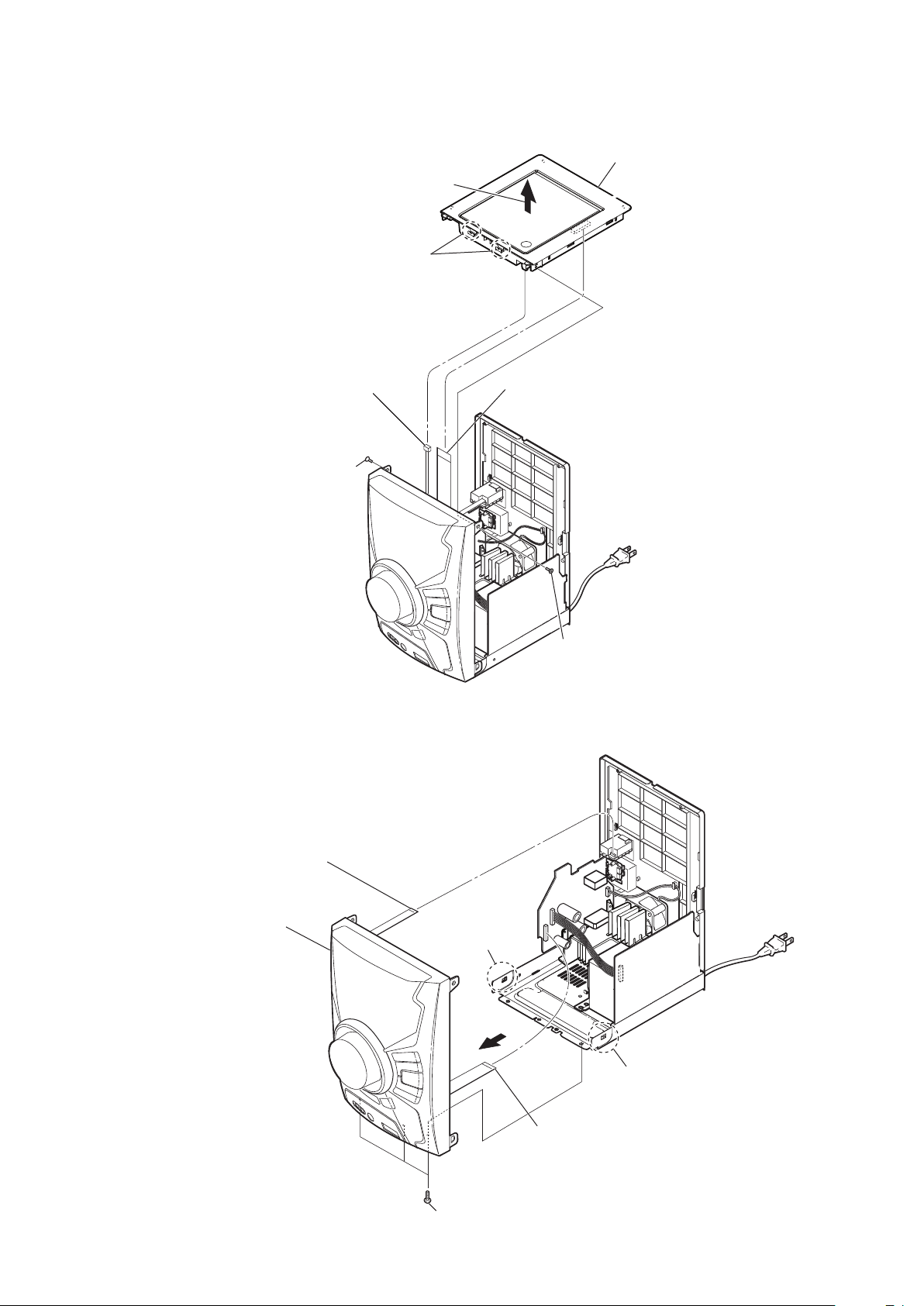
2-4. FRONT PANEL BLOCK
3 flexible flat cable (9 core)
(CN101)
front panel block
5
claw
4
screw
1
(KTP 3x10)
claw
2 flexible flat cable (21 core)
(CN704)
1 three screws
(+BVTT 3x8 type2 IT-3)
7

HCD-EC599
2-5. KNOB (VOLUME)
Note: This illustration sees the front panel block from PANEL board side.
front panel block
knob (VOLUME)
2
PANEL board
hole
2-6. POWER BOARD
5
POWER board
3
connector
(CN722)
2
two screws
+BV3 (3-CR)
Push the knob (VOLUME) by flat-head screwdriver.
1
4
connector
(CN701)
1
two screws
(+BVTP 3x8 type2 IT-3 )
8
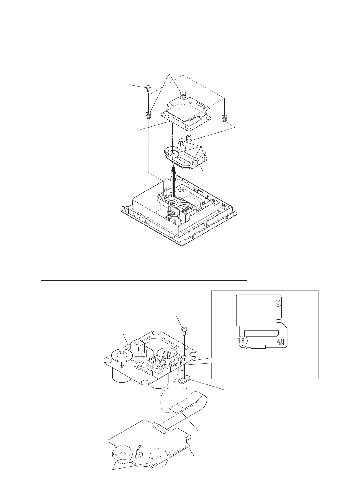
2-7. BASE UNIT (BU-D1BD76)
Note 1: This illustration sees the top panel assy from base unit side.
two insulators
4
four floating screws
1
(+PTPWHM 2.6)
base unit
7
(BU-D1BD76)
(blue)
2
two insulators
3
(gray)
four claws
5
Note 2: Four claws might be fixed by bond.
Please fix four claws by the bond
when you replace the cover (D1).
cover (D1)
6
HCD-EC599
2-8. OPTICAL PICK-UP BLOCK (DA11MMVGP)
Note 1: When disconnecting the wire (fl at type) (16 core) of optical pick-up block, solder the short-land.
tapping screw (P2)
5
optical pick-up block
7
(DA11MMVGP)
Note 2: When assembling the optical pick-up block,
remove the solder of short-land after
connecting the wire (flat type) (16 core).
shaft (support)
6
wire (flat type) (16 core) (optical pick-up)
3
Solder the short-land.
2
Remove four solders.
1
BD76 board
4
9

HCD-EC599
SECTION 3
TEST MODE
COLD RESET
The cold reset clears all data including preset data stored in the
memory to initial conditions. Execute this mode when returning
the set to the customer.
Procedure:
1. In the standby status, press [
2. Press three buttons of [
] button to turn on the system.
?/1
], [ENTER] and [
x
] simultane-
?/1
ously.
3. When “RESET” appears, the set enters standby status.
PANEL TEST MODE
This mode is used to check the Liquid crystal display, keys, destination and software version.
Enter the Panel Test Mode
Procedure:
1. In standby status, press the [
2. Press three buttons of [
x
] button to turn the power on.
?/1
], [DSGX] and [
?/1
] simultaneously.
3. All LEDs and segments of Liquid crystal display will light up.
Version Check
Procedure:
1. In the Panel test mode, press the [FUNCTION] button.
2. On the liquid crystal display panel, date and version are
displayed alternately.
3. From this status, press the [EQ] button, the destination and
model name are displayed alternately.
4. To release from this mode, press three buttons of [x], [DSGX]
and [
] simultaneously.
?/1
Key & Encoder Test check
Procedure:
1. In the Panel test mode, press the [ENTER] button.
2. The message “KEY0 0 0” displayed. Whenever any buttons
are pressed, the value is change.
3. To release from this mode, press three buttons of [x], [DSGX]
and [
] simultaneously.
?/1
COMMON TEST MODE
This mode is used to check operations of the Amplifi er section.
Procedure:
1. To enter Common Test Mode, press three buttons of [FUNCTION], [DSGX] and [
] simultaneously.
?/1
2. “COMMON” appears on the liquid crystal display panel. The
volume is changed to VOLUME MIN.
Check of Amplifi er:
1. Press [ EQ] button repeatedly until a message “EQ MAX”
appears on the liquid crystal display panel. EQ increases to
its maximum.
2. Press [EQ] button repeatedly until a message “EQ
MIN” appears on the liquid crystal display panel. EQ
decreases to its minimum.
3. Press [EQ] button repeatedly until a message “EQ
FLAT” appears on the liquid crystal display panel
GEQ is set to fl at.
4. When the [VOLUME] knob is turned clockwise even
slightly, the message “VOL MAX” appears on the liquid
crystal display panel. Sound is set to volume maximum.
5. When the [VOLUME] knob is turned clockwise even
slightly, the message “VOL 38” appears on the liquid cry
tal display panel. Sound is set to Standard Volume Position
(SVP).
6. When the [VOLUME] knob is turned counterclockwise
even slightly, the message “VOL MIN” appears on the
liquid crystal display panel. Sound is set to volume
minimum.
3. To release from this mode, press [
?/1
] button.
4. The cold reset is enforced at the same time.
TUNER STEP CHANGE
The step interval of AM channels can be toggled between 9
kHz and 10 kHz. This mode is not available for Saudi Arabian,
European and Russian models.
Procedure:
1. Press [
] button to turn on the system.
?/1
2. Press [FUNCTION] button repeatedly to select “TUNER AM”.
3. Press [
] button to turn off the system.
?/1
4. Press the [DISPLAY] button on the remote control to enter
clock mode. In clock mode, while pressing the [TUNING +
M L
] button, press the [
?/1
] button.
5. The system turns on automatically. The message “AM 9K
STEP” or “AM 10K STEP” appears on the liquid crystal
display panel and thus the channel step is changed.
CD POWER MANAGE
This mode is for switch the CD power supply on/off. Even if this
state pulls out AC plug, it is held
Procedure:
1. Press [
] button to turn on the system.
?/1
2. Press [FUNCTION] button to select CD function.
3. Press [
] button again to turn off the system.
?/1
4. Press the [DISPLAY] button on the remote control to enter
clock mode. In clock mode, while pressing the [
press the [
?/1
] button.
] button,
x
5. The systems turn on and display “CD/USB”, then display
“PWR ON” or “PWR OFF”.
CD SERVICE MODE
This mode can move the SLED of the optical pick-up and also can
turn the optical pick-up laser power on and off.
Procedure:
1. Press [
] button to turn on the system.
?/1
2. Press [FUNCTION] button to select CD function.
3. Press three buttons of [u], [+] and [
] simultaneously.
?/1
4. It enters the CD service mode and display “SERVICE”.
Key Operation:
[TUNING +
M L
], [TUNING –
l m
]:
Use these keys to move the SLED.
When [TUNING +
M L
] is pressed in this
mode, the SLED moves to outer circumference
and the message “SLED OUT” is displayed. When
[TUNING –
l m
] is pressed in this mode, the
SLED moves to inner circumference and the message “SLED IN” is displayed.
[EQ]:
Use this key to turn the optical pick-up laser power
on and off, When the laser power is turned on, the
message “LD ON” is displayed. When the laser
power is turned off, the message “LD OFF” is displayed.
5. To release from this mode, press three buttons of [
and [
] simultaneously.
?/1
u
], [+]
CD FACTORY MODE
Note 1: Do not enter this mode while any other test mode is in progress.
Note 2: Do not enter any other test mode while this mode is in progress.
Procedure:
1. Press [
2. Press [FUNCTION] button to select CD function.
] button to turn on the system.
?/1
10

HCD-EC599
3. Press three buttons of [u], [-] and [
4. It enters the CD factory mode and the message “FACTORY” is
displayed. When the [OPTIONS] button is pressed, the following message (initial display) is displayed.
] simultaneously.
?/1
– ON
S character mode setting
Tracking servo setting
RF gain setting
Key Operation:
[OPTIONS]:
The display changes in the following order when-
ever the button is pressed.
[DSGX]:
RF gain setting changes whenever the button is
“–”: No gain fi xation.
“AL”: Fix to the gain for AL disc.
“RW”: Fix to the gain for RW disc.
(Initial display)
FCSAG**(**: Focus AGC value)
TRKAG**(**: Track AGC value)
RF_AG**(**: RF AGC value)
pressed.
PROTECT KIND CHECK TEST MODE
This mode is used to check types of protect occurred during
protector on.
Procedure:
During protection on, LCD will toggle between “PROTECT”
message & type of protection mode.
Indication of LCD Type of defect Possible cause(s)
PROTECT E01 Defect of AMP
circuit
PROTECT E02 Defect of power
supply circuit
to CD
PROTECT E03 Defect of
USB+5V power
supply
PROTECT E04 Defect of 9V
power supply
PROTECT E05 AC supply
mismatch
Defect of IC701, '+'
and '-' speaker cord are
shorted, fan is blocked
from turning
Defect of optical unit,
transformer or 9V
Regulator supply
Defect of IC400 and
related circuitry
Unusual heat up of
IC702 (9V regulator)
by improper assembly
of heatsink, destruction
of IC702 etc..
Incorrect voltage
selector setting
[FUNCTION]:
S character mode setting changes whenever the but-
ton is pressed.
“ ”: S character mode OFF.
“S”: S character mode ON.
5. To release from this mode, Press three buttons of [u], [
and [
] simultaneously.
?/1
]
-
11

HCD-EC599
SECTION 4
ELECTRICAL CHECKS
CD SECTION
Note:
1. CD Block is basically constructed to operate without adjustment.
2. Use YEDS-18 disc (Part No. 3-702-101-01) unless otherwise indicated.
3. Use an oscilloscope with more than 10 MΩ impedance.
4. Clean the object lens by an applicator with neutral detergent when the
signal level is low than specifi ed value with the following checks.
5. Check the focus bias check when optical pick-up block is replaced.
FOCUS BIAS CHECK
oscilloscope
(DC range)
BD76 board
CL102 (RFOUT)
CL117 (VREF)
+
–
Procedure :
1. Connect the oscilloscope to CL102 (RFOUT) and CL117
(VREF) on the BD76UR board.
2. Press the [
] button to turn the power on, and press the
?/1
[FUNCTION] button to select CD function.
3. Set disc (YEDS-18) and press the [u] button to playback.
4. Confi rm that oscilloscope waveform is as shown in the fi gure
below (eye pattern).
A good eye pattern means that the diamond shape () in the
center of the waveform can be clearly distinguished.
VOLT/DIV: 200 mV
TIME/DIV: 500 ns
TUNER SECTION
0 dB = 1 V
FM AUTO STOP CHECK
signal
generator
set
Procedure :
1. Turn the power on.
2. Input the following signal from Signal Generator to FM antenna input directly.
Carrier frequency : A = 87.5 MHz, B = 98 MHz, C = 108 MHz
Deviation : 75 kHz
Modulation : 1 kHz
ANT input : 35 dBu (EMF)
Note: Please use 75 ohm “coaxial cable” to connect SG and the set. You
cannot use video cable for checking.
Please use SG whose output impedance is 75 ohm.
3. Set to FM tuner function and scan the input FM signal with
automatic scanning.
4. Confi rm that input Frequency of A, B and C detected and auto-
matic scanning stops.
The stop of automatic scanning means “The station signal is
received in good condition”.
Checking Location:
-BD76 Board (SideB)-
CL102
(RFOUT)
IC101
CL117
(VREF)
level:
1.1 ± 0.4 Vp-p
12

5-1. BLOCK DIAGRAM – CD/USB Section –
OPTICAL PICK-UP BLOCK
(DA11MMVGP)
A
B
C
D
E
F
AUTOMATIC
LD
MD
VREF
SP+
SP-
SL+
SL-
T+
T-
F+
F-
POWER
CONTROL
Q201
FOCUS/TRACKING COIL DRIVE,
SPINDLE/SLED MOTOR DRIVE
IC301
BIAS
23
VO1+2
VO1-
1
VO2+11
VO2-
12
VO3+18
VO3-
17
VO4+26
VO4-
27
IN2’
IN3’
IN4’
MUTE
3
IN1
9
20
24
7
5AIN
BIN
7
6CIN
8DIN
EIN
13
FIN
14
18 LDD
19
LDS
11 VREF
25 SPDO
24 SLDO
23 TDO
22 FDO
USB CONTROL
IC901
CD-MP3 PROCESSOR
IC101
SECTION 5
DIAGRAMS
LCHO
76
RCHO R-ch78
47
RESB
LIMIT-SW
32
XOUT
72
X101
XIN
16.934MHz
73
S001
(LIMIT)
CD OPEN/CLOSE
DET SWITCH
(SW305)
2
O-CD-RST
I-CDM-SW
88
O-CD-M-MUTE
1
SYSTEM CONTROL
IC100 (1/3)
CD/USB-L
A
HCD-EC599
MAIN
Section
(Page 14)
CN400
3
D+
2
D-
1
(USB)
4
5FKLVRPLWWHGGXHWRVDPHDV/FK
6LJQDOSDWK
: AUDIO
: FM/AM
: CD
: USB
VBUS+5V
X901
12MHz
38 UHD+
37 UHD-
CF1
6
CF2
7
LRCK 28
BCLK
SDAT
P20
P70
P24
P22
SI0 10
SO0
SCK0
P16 15
URX1
UTX1
P71
RES 2
DBGP0
DBGP1
DBGP2 25
PCMLRSY
62
PCMBCK
27
26
32
46
33
31
9
11
44
45
47
23
24
63
64
65
33
34
35
PCMDATA
PCMREQ
STREQ
STCK
STDATA
TRESET
DBGP0
DBGP1
DBGP2
43CE
44CL
45DI
46DO
9
CN901
8
FLASH
7
( )
PROGRAMMING
5
6
O-CD-CE
5
O-CD-CLK
O-CD-DI
4
3
I-CD-DO
O-USB-TXD93
94
I-USB-RXD
O-USB-SLEEP
7
O-USB-RST8
DGBP0
DGBP1
DGBP2
2
95
96
97
DGBP0
DGBP1
DGBP2
RESET
3
5
1
RESET
CN100
FLASH
( )
PROGRAMMING
DISPLAY/POWER
B
(Page 15)
Section
HCD-EC599
13
13
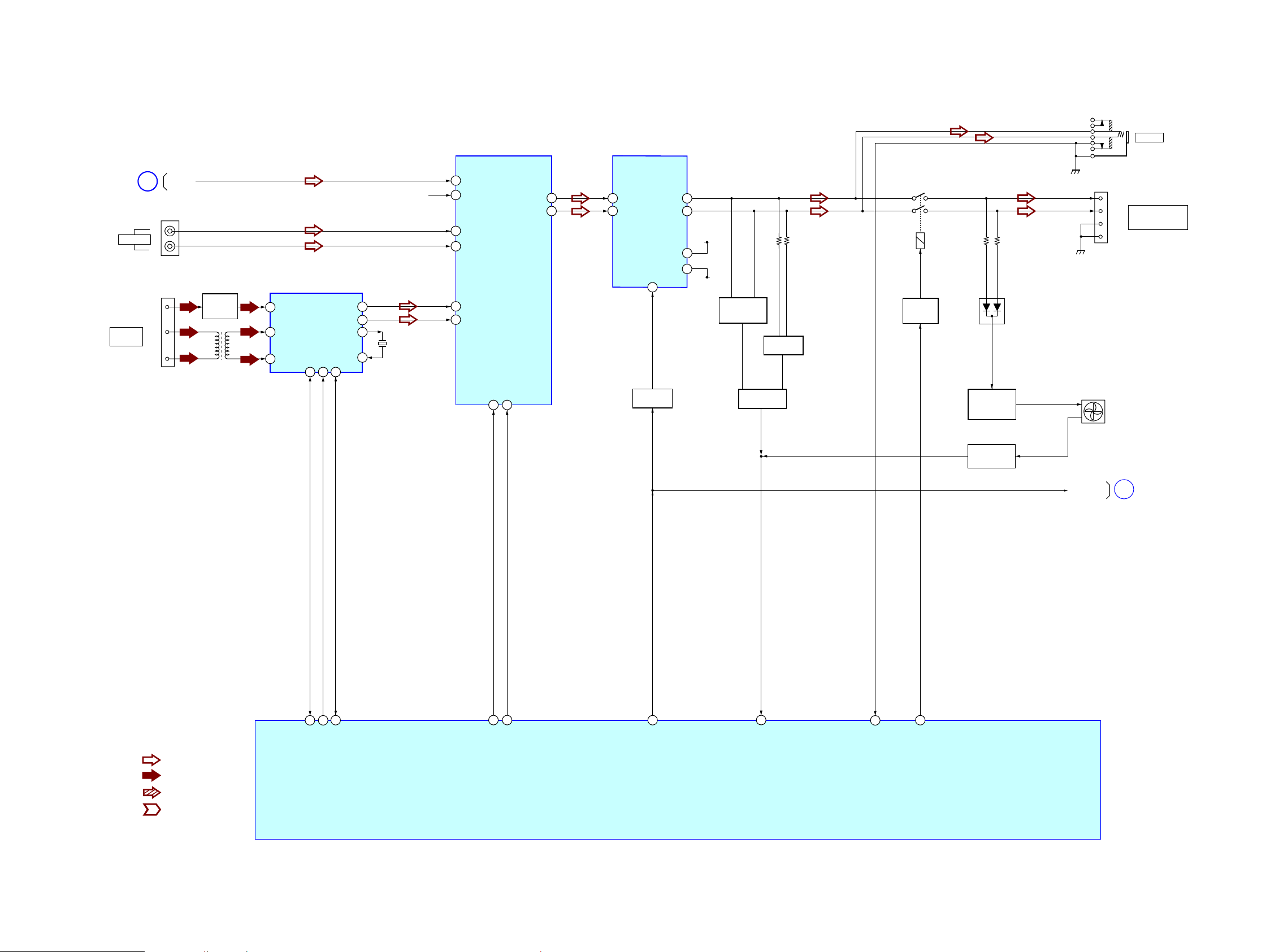
HCD-EC599
5-2. BLOCK DIAGRAM – MAIN Section –
J380
CD/USB
Section
(Page 13)
DVD/PC IN
ANTENNA
FM/AM
INPUT SELECTOR
IC500
CD/USB-L
A
R-ch
J500
L
R
AM/FM-DET,OSC,MIX,PLL,IF AMP
CN103
3
FM
2
AM
1
AM
FL101
BAND-PASS
FILTER
L101
4
7
6
FRF1
ARF2
ARF1
IC101
LOUT
ROUT
IIC/RDSI
8CK10DA13
15
14
X1
18
X2
19
X101
32.768kHz
32
31
5
6
9
10
CD/USB-L
CD/USB-R
PC-IN-L
PC-IN-R
TUNER-L
TUNER-R
SCLK
27 28
SDATA
OUT-L
OUT-R
25
21
11
15
POWER AMP
LCH IN
RCH IN
IC701
RCH OUT-
LCH OUT-
STBY
13
STBY SW
Q712
+VCC
-VCC
TB701
7
5
+VCC
3
2
-VCC
OVERLOAD
DETECT
Q715,Q716
DC DETECT
Q705,Q707
PROTECT
Q704,Q708
RELAY
DRIVE
Q713
RY600
FAN MOTOR
DRIVE
Q709,Q710
Q720,Q721
FAN MOTOR
DETECT
Q711
D721
4
3
2
1
STBY RELAY
PHONES
+ R
+ L
IMPEDANCE: USE 6ȍ
– R
– L
DC FAN
DISPLAY/POWER
C
SPEAKERS
Section
(Page 15)
HCD-EC599
SignaO Sath
: AUDIO
: FM/AM
: CD
: USB
91
92
I2C-TU-CLK
I2C-TU-DATA
41
I-TU-RDS
98
99
I2C-FUNC-CLK
I2C-FUNC-DATA
SYSTEM CONTROL
1414
30
O-STBY-RELAY
IC100 (2/3)
34
I-PROTECT
35
I-HP-DET
31
O-SPK-RELAY
 Loading...