

Page 1

HCD-EC55/EC77/GX99
SERVICE MANUAL
Ver. 1.1 2007.04
• HCD-EC55 (US model) and HCD-EC77/GX99 (US
and Canadian models) are the Amplifier, CD pla yer
and Tuner section in MHC-EC55/EC77/GX99.
• HCD-EC55 (Except US model) and HCD-EC77/
GX99 (Except US and Canadian models) are the
Amplifier, CD player, Tape Deck and Tuner section
in MHC-EC55/EC77/GX99.
Photo : HCD-EC55 (E model)
CD
Section
TAPE Model Name Using Similar Mechanism NEW
Section T ape Transport Mechanism T ype CS-21SC-901TP
US Model
HCD-EC55/EC77/GX99
Canadian Model
HCD-EC77/GX99
AEP Model
HCD-EC55/EC77
UK Model
HCD-EC55
E Model
Australian Model
HCD-EC55/EC77
Model Name Using Similar Mechanism NEW
Base Unit Name BU-K6BD90-WOD
Optical Pick-up Name KSM-213DCP
Main unit
AUDIO POWER SPECIFICATIONS
POWER OUTPUT AND TOTAL HARMONIC DISTORTION:
(HCD-GX99, HCD-EC77 The United States model only)
Low channel
With 8 ohm loads, both channels driven, from 120 – 10,000 Hz; 60 watts
per channel minimum RMS power, with no more than 0.7% total harmonic
distortion from 250 milliwatts to rated output.
High channel
With 8 ohm loads, both channels driven, from 2,000 – 13,000 Hz; 60 watts
per channel minimum RMS power, with no more than 0.7% total harmonic
distortion from 250 milliwatts to rated output.
AUDIO POWER SPECIFICATIONS
POWER OUTPUT AND TOTAL HARMONIC DISTORTION:
(HCD-EC55 The United States model only)
With 6 ohm loads, both channels driven, from 120 – 10,000 Hz; 45 watts
per channel minimum RMS power, with no more than 0.7% total harmonic
distortion from 250 milliwatts to rated output.
Amplifier section
HCD-GX99
Front speaker:
RMS output power (reference):
Low channel
95 W + 95 W (per channel at 8 Ω, 1 kHz, 10% THD)
High channel
95 W + 95 W (per channel at 8 Ω, 8 kHz, 10% THD)
Subwoofer:
RMS output power (reference):
150 W (at 6 Ω, 80 Hz, 10% THD)
HCD-EC77
North American model:
RMS output power (reference):
Low channel
95 W + 95 W (per channel at 8 Ω, 1 kHz, 10% THD)
High channel
95 W + 95 W (per channel at 8 Ω, 8 kHz, 10% THD)
SPECIFICATIONS
European and Russian models:
Power output (rated):
Low channel
45 W + 45 W (at 8 Ω, 1 kHz, 1% THD)
High channel
45 W + 45 W (at 8 Ω, 8 kHz, 1% THD)
RMS output power (reference):
Low channel
65 W + 65 W (per channel at 8 Ω, 1 kHz, 10% THD)
High channel
65 W + 65 W (per channel at 8 Ω, 8 kHz, 10% THD)
Other models:
The following are measured at AC 120, 127, 220, 240 V, 50/60 Hz
Power output (rated):
Low channel
50 W + 50 W (at 8 Ω, 1 kHz, 1% THD)
High channel
50 W + 50 W (at 8 Ω, 8 kHz, 1% THD)
RMS output power (reference):
Low channel
70 W + 70 W (per channel at 8 Ω, 1 kHz, 10% THD)
High channel
70 W + 70 W (per channel at 8 Ω, 8 kHz, 10% THD)
HCD-EC55
North American model:
RMS output power (reference):
65 W+ 65 W (per channel at 6 Ω, 1 kHz, 10% THD)
European and Russian models:
Power output (rated): 45 W + 45 W (at 6 Ω, 1 kHz, 1% THD)
RMS output power (reference):
65 W + 65 W (per channel at 6 Ω, 1 kHz, 10% THD)
Other models:
The following are measured at AC 120, 127, 220, 240 V, 50/60 Hz
Power output (rated): 45 W + 45 W (at 6 Ω, 1 kHz, 1% THD)
RMS output power (reference):
65 W + 65 W (per channel at 6 Ω, 1 kHz, 10% THD)
Inputs
AUDIO IN (stereo mini jack): Sensitivity 800 mV,
impedance 47 kilohms
Outputs
PHONES (stereo mini jack): Accepts headphones with
an impedance of 8 Ω or more
SPEAKER: Accepts impedance of 6 to 8 Ω
SUBWOOFER OUT (HCD-GX99 only)
CD player section
System: Compact disc and digital audio system
Laser: Semiconductor laser (λ=770 – 810 nm)
Emission duration: continuous
Frequency response: 20 Hz – 20 kHz
Signal-to-noise ratio: More than 90 dB
Dynamic range: More than 88 dB
Tape deck section (Except for NorthAmerican model)
Recording system: 4-track 2-channel, stereo
Tuner section
FM stereo, FM/AM superheterodyne tuner
Antenna:
FM lead antenna
AM loop antenna
FM tuner section:
Tuning range
North American model: 87.5 – 108.0 MHz (100 kHz step)
Other models: 87.5 – 108.0 MHz (50 kHz step)
Intermediate frequency: 10.7 MHz
— Continued on next page —
9-887-532-02
2007D16-1
© 2007.04
COMPACT DISC DECK RECEIVER
Sony Corporation
Home Audio Division
Published by Sony Techno Create Corporation
Page 2
HCD-EC55/EC77/GX99
Ver. 1.1
AM tuner section:
Tuning range
Pan-American and Australian models:
530 – 1,710 kHz (with 10 kHz tuning interval)
531 – 1,710 kHz (with 9 kHz tuning interval)
European and Russian models:
531 – 1,602 kHz (with 9 kHz tuning interval)
Other models:
530 – 1,610 kHz (with 10 kHz tuning interval)
531 – 1,602 kHz (with 9 kHz tuning interval)
Intermediate frequency: 450 kHz
General
Powerrequirements:
North American model: AC 120 V, 60 Hz
European and Russian models: AC 230 V, 50/60 Hz
Australian model: AC 230 – 240 V, 50/60 Hz
Mexican model: AC 127 V, 60 Hz
Argentine model: A C 220 V, 50/60 Hz
Korean model: A C 220 V, 60 Hz
Other models: AC 120, 220 or 230 – 240 V, 50/60 Hz, adjustable with voltage
selector
Power consumption:
HCD-GX99
USA model: 190 W
Canadian model: 245 VA
HCD-EC77
USA model: 190 W
Canadian model: 245 VA
European and Russian models: 140 W
Other models: 150 W
HCD-EC55
USA model: 95 W
European and Russian models: 95 W
Other models: 95 W
Dimensions (w/h/d)(excl. speakers):
Approx. 200 × 306 × 410 mm
Mass (excl. speakers):
HCD-GX99
North American model: Approx. 6.1 kg
HCD-EC77
North American and European models: Approx. 6.1 kg
Other models: Approx. 6.4 kg
HCD-EC55
North American model: Approx. 5.0 kg
Other models: Approx. 5.3 kg
Design and specifications are subject to change without notice.
0.5 W (in Power Saving Mode)
0.5 W (in Power Saving Mode)
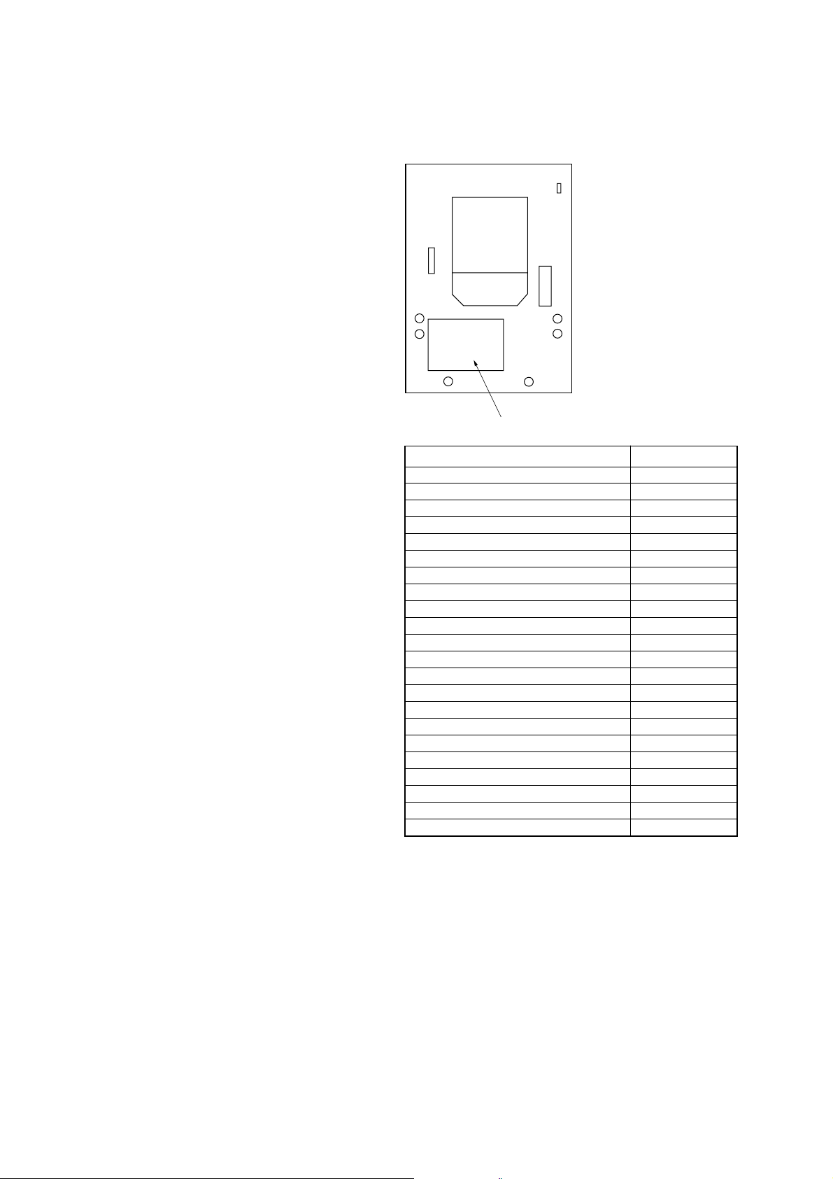
MODEL IDENTIFICATION
– Back Panel –
Parts No.
Model Part No.
GX99: CND model 2-319-061-0[]
EC55: AEP, UK model 2-893-579-0[]
EC55: RU model 2-893-580-0[]
EC55: E2 model 2-893-581-0[]
EC55: E51 model 2-893-582-0[]
EC55: MX model 2-893-583-0[]
EC55: AR model 2-893-584-0[]
EC55: SP model 2-893-586-0[]
EC55: AUS model 2-893-587-0[]
EC55: KR model 2-893-588-0[]
EC77: CND model 2-893-595-0[]
EC77: RU model 2-893-597-0[]
EC77: E2 model 2-893-598-0[]
EC77: E51 model 2-893-599-0[]
EC77: MX model 2-893-600-0[]
EC77: AR model 2-893-601-0[]
EC77: AUS model 2-893-604-0[]
EC55: US model 3-095-136-0[]
EC77: AEP model 3-095-137-0[]
EC77: E3 model 3-095-138-0[]
GX99: US model 3-095-139-0[]
EC77: US model 3-095-495-0[]
SAFETY-RELATED COMPONENT WARNING!!
COMPONENTS IDENTIFIED BY MARK 0 OR DOTTED LINE
WITH MARK 0 ON THE SCHEMATIC DIAGRAMS AND IN
THE PARTS LIST ARE CRITICAL TO SAFE OPERATION.
REPLACE THESE COMPONENTS WITH SONY PARTS WHOSE
PART NUMBERS APPEAR AS SHOWN IN THIS MANUAL OR
IN SUPPLEMENTS PUBLISHED BY SONY.
ATTENTION AU COMPOSANT AYANT RAPPORT
À LA SÉCURITÉ!
LES COMPOSANTS IDENTIFIÉS PAR UNE MARQUE 0 SUR
LES DIAGRAMMES SCHÉMATIQUES ET LA LISTE DES
PIÈCES SONT CRITIQUES POUR LA SÉCURITÉ DE
FONCTIONNEMENT. NE REMPLACER CES COM- POSANTS
QUE PAR DES PIÈCES SONY DONT LES NUMÉROS SONT
DONNÉS DANS CE MANUEL OU D ANS LES SUPPLÉMENTS
PUBLIÉS PAR SONY.
2
•Abbreviation
AR : Argentine model
AUS:Australian model
CND : Canadian model
E2 : 120 V AC area in E model
E3 : 240 V AC area in E model
E51 : Chilean and Peruvian models
KR : Korean model
MX : Mexican model
RU : Russian model
SP : Singapore model
Page 3

TABLE OF CONTENTS
HCD-EC55/EC77/GX99
1. SERVICING NOTES ................................................ 4
2. GENERAL ................................................................... 6
3. DISASSEMBLY
3-1. Disassembly Flow ........................................................... 8
3-2. Side Panel (R), Side Panel (L)......................................... 9
3-3. Top Panel Assy (Except US, CND) ................................. 10
3-4. Top Panel (US, CND)...................................................... 10
3-5. Front Panel Assy.............................................................. 11
3-6. Mechanical Deck (Except US, CND).............................. 12
3-7. Belt (MAIN), Belt (R/F) (Except US, CND) .................. 12
3-8. KEY-LEFT Board............................................................ 13
3-9. KEY-RIGHT Board, KEY-CD Board, PANEL Board .... 13
3-10. JACK Board..................................................................... 14
3-11. MAIN Board.................................................................... 15
3-12. CD Mechanical................................................................ 16
3-13. Optical Pick-up (KSM-213DCP), BD90 Board .............. 17
3-14. Belt (DLM3A) ................................................................. 18
3-15. Chassis............................................................................. 18
3-16. PT Board (Except EC55:US), PT (U) Board (EC55:US),
Power Transformer .......................................................... 19
3-17. LOW-AMP Board, HI-AMP Board (EC77/GX99) ......... 19
3-18. HI-AMP Board (EC55) ................................................... 20
3-19. DC Fan ............................................................................ 20
4. TEST MODE ............................................................... 21
5. MECHANICAL ADJUSTMENTS......................... 25
6. ELECTRICAL ADJUSTMENTS .......................... 25
7. DIAGRAMS
7-1. Block Diagram — BD/DRIVER Section — .................. 30
7-2. Block Diagram — TUNER Section — .......................... 31
7-3. Block Diagram — MAIN Section — ............................. 32
7-4. Printed Wiring Board — BD90 Board — ...................... 33
7-5. Schematic Diagram — BD90 Board — ......................... 34
7-6. Printed Wiring Boards — MAIN Section — ................. 35
7-7. Schematic Diagram — MAIN Section (1/2) — ............. 36
7-8. Schematic Diagram — MAIN Section (2/2) — ............. 37
7-9. Printed Wiring Board — PANEL Board — ................... 38
7-10. Schematic Diagram — PANEL Board — ...................... 39
7-11. Printed Wiring Boards — KEY Section — .................... 40
7-12. Schematic Diagram — KEY Section — ........................ 40
7-13. Printed Wiring Board — HI-AMP Board —.................. 41
7-14. Schematic Diagram — HI-AMP Board — .................... 42
7-15. Printed Wiring Board
— LOW-AMP Board (EC77/GX99) — .......................... 43
7-16. Schematic Diagram
— LOW-AMP Board (EC77/GX99) — .......................... 44
7-17. Printed Wiring Boards
— DECK Section (Except US,CND) —......................... 45
7-18. Schematic Diagram
— DECK Section (Except US,CND) —......................... 45
7-19. Printed Wiring Board
— PT Board (Except EC55: US) — ............................... 46
7-20. Schematic Diagram
— PT Board (Except EC55: US) — ............................... 46
7-21. Printed Wiring Board — PT (U) Board (EC55: US) —. 47
7-22. Schematic Diagram — PT (U) Board (EC55: US) — ... 47
8. EXPLODED VIEWS
8-1. Overall Section ................................................................ 57
8-2. Front Panel Section ......................................................... 58
8-3. Chassis Section (EC77/GX99) ........................................ 59
8-4. Chassis Section (EC55) ................................................... 60
8-5. Top Section (Except US, CND)....................................... 61
8-6. CD Mechanism Deck Section ......................................... 62
9. ELECTRICAL PARTS LIST .................................. 63
3
Page 4

HCD-EC55/EC77/GX99
r
SECTION 1
SERVICING NOTES
CAUTION
Use of controls or adjustments or performance of procedures
other than those specified herein may result in hazardous radiation
exposure.
Notes on chip component replacement
• Never reuse a disconnected chip component.
• Notice that the minus side of a tantalum capacitor may be
damaged by heat.
Flexible Circuit Board Repairing
• Keep the temperature of the soldering iron around 270 °C
during repairing.
• Do not touch the soldering iron on the same conductor of the
circuit board (within 3 times).
• Be careful not to apply force on the conductor when soldering
or unsoldering.
SAFETY CHECK-OUT
After correcting the original service problem, perform the following
safety check before releasing the set to the customer:
Check the antenna terminals, metal trim, “metallized” knobs, screws,
and all other exposed metal parts for AC leakage.
Check leakage as described below.
LEAKAGE TEST
The AC leakage from any exposed metal part to earth ground and
from all exposed metal parts to any exposed metal part having a
return to chassis, must not exceed 0.5 mA (500 microamperes.).
Leakage current can be measured by any one of three methods.
1. A commercial leakage tester, such as the Simpson 229 or RCA
WT -540A. Follow the manuf acturers’ instructions to use these
instruments.
2. A battery-operated AC milliammeter . The Data Precision 245
digital multimeter is suitable for this job.
3. Measuring the voltage drop across a resistor by means of a
VOM or battery-operated AC v oltmeter. The “limit” indication
is 0.75 V, so analog meters must hav e an accurate low-v oltage
scale. The Simpson 250 and Sanwa SH-63Trd are examples
of a passive VOM that is suitable. Nearly all battery operated
digital multimeters that have a 2 V A C range are suitable. (See
Fig. A)
To Exposed Metal
Parts on Set
AC
0.15 µF
1.5 k
Ω
Earth Ground
voltmete
(0.75 V)
Fig. A. Using an AC voltmeter to check AC leakage.
This appliance is classified as a CLASS 1 LASER product.
The CLASS 1 LASER PRODUCT MARKING is located on
the rear exterior.
Laser component in this product is capable of emitting radiation
exceeding the limit for Class 1.
NOTES ON HANDLING THE OPTICAL PICK-UP
BLOCK OR BASE UNIT
The laser diode in the optical pick-up block may suffer electrostatic
break-down because of the potential difference generated by the
charged electrostatic load, etc. on clothing and the human body.
During repair, pay attention to electrostatic break-down and also
use the procedure in the printed matter which is included in the
repair parts.
The flexible board is easily damaged and should be handled with
care.
NOTES ON LASER DIODE EMISSION CHECK
The laser beam on this model is concentrated so as to be focused on
the disc reflective surface by the objective lens in the optical pickup block. Therefore, when checking the laser diode emission,
observe from more than 30 cm away from the objective lens.
LASER DIODE AND FOCUS SEARCH OPERATION
CHECK
Carry out the “S curve check” in “CD section adjustment” and check
that the S curve waveforms is output three times.
UNLEADED SOLDER
Boards requiring use of unleaded solder are printed with the leadfree mark (LF) indicating the solder contains no lead.
(Caution: Some printed circuit boards may not come printed with
the lead free mark due to their particular size)
: LEAD FREE MARK
Unleaded solder has the following characteristics.
• Unleaded solder melts at a temperature about 40 °C higher
than ordinary solder.
Ordinary soldering irons can be used but the iron tip has to be
applied to the solder joint for a slightly longer time.
Soldering irons using a temperature regulator should be set to
about 350 °C.
Caution: The printed pattern (copper foil) may peel away if
the heated tip is applied for too long, so be careful!
• Strong viscosity
Unleaded solder is more viscou-s (sticky, less prone to flow)
than ordinary solder so use caution not to let solder bridges
occur such as on IC pins, etc.
• Usable with ordinary solder
It is best to use only unleaded solder but unleaded solder may
also be added to ordinary solder.
CAUTION
When carrying this system
1
Remove all discs to protect the CD mechanism.
2
Hold down CD u (play/pause) on the unit, and press
?/1 until “STANDBY” appears.
3
After “LOCK” appears, unplug the power cord.
4
Page 5
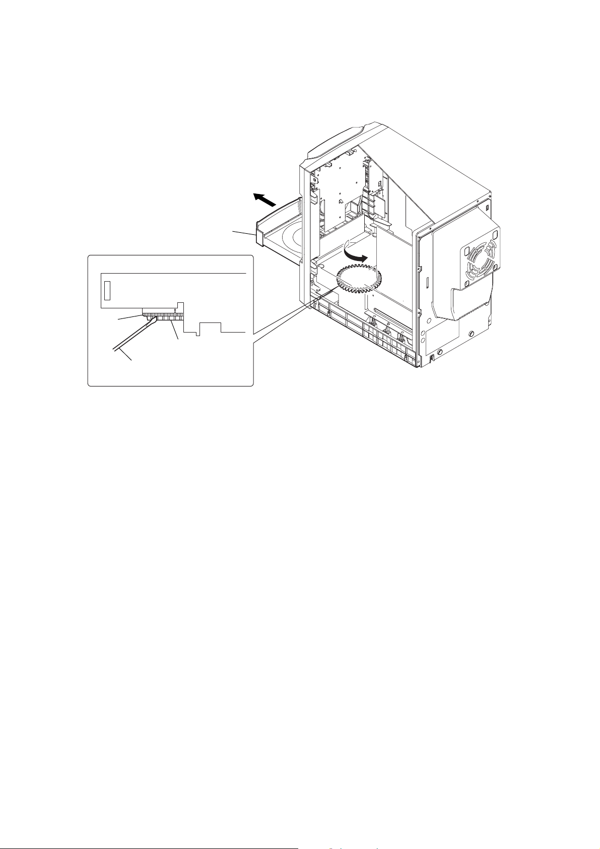
HOW TO OPEN THE DISC TRAY WHEN POWER SWITCH TURNS OFF
Turn the bottom rib (not the gear) with a flathead screwdriver in the direction of arrow A, and
draw out the tray in the direction of arrow B.
B
tray
A
HCD-EC55/EC77/GX99
gear
bottom rib
flathead screwdriver
5
Page 6

HCD-EC55/EC77/GX99
Basic Operations
*
*Except for North American model
SECTION 2
GENERAL
Adjusting the sound
To adjust the volume
Press VOLUME +/– on the remote (or turn the
VOLUME control on the unit)
To add a sound eect
To Pr ess
Generate a more dynamic
sound (Dynamic Sound
Generator X-tra)
Set the sound eect
To turn on the subwoofer
Press SUBWOOFER ON/OFF in the lower part of the
subwoofer until the indicator on the subwoofer lights up.
*To adjust the sound output level for the subwoofer, turn the
SUBWOOFER LEVEL in the lower part of the subwoofer. Once you
have made the adjustment, the overall sound level can be adjusted
using VOLUME +/– on the remote (or turn the VOLUME control
ȶ
on the unit)
.
Playing a CD/MP3 disc
1
Select the CD function.
Press CD on the remote (or FUNCTION repeatedly)
Ȭ
.
2
Place a disc.
Press ì (open/close)
disc with the label side up on the disc tray. To place
additional discs, slide the disc tray with your nger as
shown below.
To c lo se the disc tray, press ì (open/close)
unit.
Do not force the disc tray closed with your nger, as
this may damage the unit.
ȶ
.
Ȱ
DSGX
Ȱ
EQ
.
(HCD-GX99 only)
ȱ
on the unit, and place a
on the unit.
ȱ
on the
This section is extracted
from instruction manual.
Notes on playing multisession discs
ˎIf the disc begins with a CD-DA (or MP3) session, it is recognized
as a CD-DA (or MP3) disc, and playback continues until another
session is encountered.
ˎA disc with a mixed CD format is recognized as a CD-DA (audio)
disc.
Listening to the radio
1
Select “FM” or “AM.”
Press TUNER/BAND
2
Select the tuning mode.
Press TUNING MODE
appears.
3
Tune in the desired station.
Press +/– on the remote (or TUNING + or – on the
ȭ
unit)
Scanning stops automatically when a station is tuned
in, and then “TUNED” and “STEREO” (for stereo
programs) appear.
To stop automatic scanning
Press Ą (stop) ȭ.
To tune in a station with a weak signal
If “TUNED” does not appear and the scanning does
not stop, press TUNING MODE
“MANUAL” appears and press +/– on the remote (or
TUNING + or – on the unit)
desired station.
To reduce static noise on a weak FM stereo
station
Press FM MODE Ȯ on the remote repeatedly until
“MONO” appears to turn o stereo reception.
Ȭ
repeatedly.
Ȯ
repeatedly until “AUTO”
.
Ȯ
repeatedly until
ȭ
repeatedly to tune in the
Before using the system
To use the remote
Slide and remove the battery compartment lid Ȼ, and
insert the two R6 (size AA) batteries (supplied), × side
rst, matching the polarities shown below.
Notes on using the remote
ˎWith normal use, the batteries should last for about six months.
ˎDo not mix an old battery with a new one or mix dierent types of
batteries.
ˎIf you do not use the remote for a long period of time, remove the
batteries to avoid damage from batter y leakage and corrosion.
ˎBatteries installed devices shall not be exposed to excessive heat such
as sunshine, re or the like.
To set the clock
1
Turn on the system.
Press ÒÄÆ (on/standby)
2
Select the clock set mode.
Press CLOCK/TIMER SET
current mode appears on the display, press Ã/Ñ
ȭ
on the remote repeatedly to select “CLOCK,” and
then press ENTER
3
Set the time.
Press Ã/Ñ
the hour, and then press ENTER
Use t he same procedure to set the minutes.
e clock settings are lost when you disconnect the
power cord or if a power failure occurs.
ȩ
.
ȹ
on the remote. If the
Ⱥ
on the remote.
ȭ
on the remote repeatedly to set
Ⱥ
on the remote.
Selecting a music source
Ȭ
on the remote.
Ȭ
3)
on
until
Ȭ
Ȭ
.
Press the following buttons (or press FUNCTION
repeatedly).
To select Press
CD
Tun e r
1)
Tap e
2)
(connected
Component
using an audio cord)
1)
Except for North American model.
2)
If the component has the AVLS (Automatic Volume Limiter System)
or BASS BOOST function, turn o the function to avoid distorted
sound from the speakers.
3)
North American model only.
CD
TUNER/BAND
TAP E Ȭ on the remote.
FUNCTION repeatedly
(or AUDIO IN
the remote)
“AU D I O IN” appears.
3
Select a disc.
If the discs are currently stopped, press DISC SKIP on
the remote (or DISC SKIP/EX-CHANGE on the unit)
ȳ
. To change discs while in other func tions, press
Ȳ
on the unit.
DISC 1 – 3
4
Start playback.
Press à (play) (or CD ā (play/pause) on the unit)
Ȭ
.
To e xc hange othe r discs during playback, press DISC
SKIP/EX-CHANGE
To Pr ess
Pause playb ack
Stop playback
Select a folder on an
MP3 disc
Select a track or le
Find a point in a
track or le
Select Repeat Play
To change the play mode
Press PLAY MODE Ȯ repeatedly while the player is
stopped. You can select normal play (no display for all
discs or “1 DISC” for a disc or “
in the folder on the disc), shue play (“SHUF” for
all discs shue, “1 DISC SHUF” for one disc shue
SHUF*” for folder shue), or program play
or “
(“PGM”).
*When playing a CD-DA disc, (SHUF) Play performs the same
operation as 1 DISC (SHUF) Play.
Notes on Repeat Play
ˎAll tracks or les on a disc are played repeatedly up to ve times.
ˎYo u cannot select “REP” and “SHUF” (all discs shue) at the same
time.
ˎ“REP1” indicates that a single track or le is repeated until you stop
it.
Notes on playing MP3 discs
ˎDo not save other types of tracks or les or unnecessary folders on a
disc that has MP3 les.
ˎFolders that have no MP3 les are skipped.
ˎMP3 les are played back in the order that they are recorded onto
the disc.
ˎe system can only play MP3 les that have a le extension of
“.MP3”.
ˎIf there are les on the disc that have the “.MP3” le extension,
but that are not MP3 les, the unit may produce noise or may
malfunction.
ˎe maximum number of:
ˋloadable sessions on a single disc is 10.
ˋfolders is 150 (including the root folder).
ˋMP3 les is 255.
ˋMP3 les and folders that can be contained on a single disc is 300.
ˋfolder levels (the tree structure of les) is eight.
ˎCompatibility with all MP3 encoding/writing soware, recording
device, and recording media cannot be guaranteed. Incompatible
MP3 discs may produce noise or interrupted audio or may not play
at all.
ȳ
on the unit.
ê (pause) on the remote (or CD
ā on the unit)
play, press the button again.
Ą (stop)
Ȭ
. To resume
ȭ
.
+/– ȯ.
ÃÄÑ (go back/go forward)
on the remote (øÄÞ on the
ȭ
.
unit)
Hold down ù/ß (rewind/fast
ȭ
during playback, and
forward)
release the button at the desired
point.
Ȯ
on the remote
REPEAT
repeatedly until “REP” or “REP1”
appears.
” for all MP3 les
Playing a tape (Except for North
American model)
1
Select a tape function.
Press TAPE on the remote (or FUNCTION on the
unit repeatedly)
2
Insert a tape.
Press Ąì (stop/eject)
tape into the cassette holder. Make sure there is no
slack in the tape to avoid damaging the tape or the
tape deck.
3
Start playback.
Press à (play)
To Pr ess
Pause playb ack
Stop playback
Rewind or fast
forward*
*Be sure to press Ąì (stop/eject) ȫ on the unit aer the tape has
been wound or rewound to the end.
Note
Do not turn o the system during playback or recording.
Ȭ
.
ȫ
on the unit, and insert the
ȫ
on the unit.
ȫ
ê (pause)
on the unit. To resume
play, press the button again.
Ąì (stop/eject)
ù/ß
ȫ
on the unit.
ȫ
on the unit.
Changing the display
To Pr ess
Change
information on the
display*
Change Display
mode (See below.)
*For example, you can view CD/MP3 disc information, such as the
track or le number or folder name during normal play, or the total
playing time while the player is stopped.
e system oers the following display modes.
Display mode When the system is o1),
Power Saving
2)
Mode
3)
Clock
1)
e STANDBY indicator on the unit lights up when the system is
o.
2)
You ca nnot set the clock in Power Saving Mode.
3)
e clock display automatically turns to Power Saving Mode aer
eight seconds.
Notes on the display information
ˎCharacters that cannot be displayed appear as “_”.
ˎe following are not displayed;
ˋtotal playing time for an MP3 disc.
ˋremaining playing time for an MP3 le.
ˎe following are not displayed correctly;
ˋelapsed playing time of an MP3 le encoded using a VBR (variable
bit rate).
ˋfolder and le names that do not follow either the ISO9660 Level
1, Level 2 or Joliet in the expansion format.
ˎe following are displayed;
ˋtotal playing time for a CD-DA disc when the play mode is “1
DISC”.
ˋremaining playing time for a track.
ˋID3 tag information for MP3 les when ID3 version 1 and version
2 tags are used (ID3 version 2 tag information display has priority
when both ID3 version 1 and version 2 tags are used for a single
MP3 le).
ˋup to 15 characters of ID3 tag information using uppercase letters
(A to Z), numbers (0 to 9), and symbols (‘< > * + , – / @ [ \ ] _).
repeatedly when the
DISPLAY
system is turned on.
repeatedly when the
DISPLAY
system is turned o.
e display is turned o to conserve
power. e timer and clock continue
to operate.
e clock is displayed.
6
Page 7

Using optional audio components
Recording onto a tape (Except for
North American model)
Use a TYPE I (normal) tape only.
You c an record just the portions you like from a sound
source, including connected audio components.
Use b utton s on the unit to control tape recording.
1
Insert a recordable tape into the cassette holder
with the side you want to record facing up.
2
Prepare the recording source.
Select the desired source to record.
Place the disc you want to record and press DISC
SKIP/EX-CHANGE
ȳ
to select a disc.
When recording a folder from an MP3 disc, press
PLAY MODE
Ȯ
repeatedly to select “ ,” a nd then
press
+/– ȯ repeatedly to select the desired
folder.
To record only your favorite CD tracks or MP3 les in
your desired order, perform steps 2 to 5 of “Creating
your own CD program.”
3
Start recording.
Press Ć (record)
ȫ
, and then start playing the
desired recording source.
e CD starts playing automatically aer 10 seconds
have passed.
If there is noise while recording from the tuner,
reposition the appropriate antenna to reduce the
noise.
While recording, you cannot listen to other sources.
To s top recording
Press Ąìȫ.
Tip
We r ecommend that you press êȫ rst, and then press Ąìȫ to
avoid noise being recorded when you stop recording.
Using the timers
e system oers two timer functions. If you use both
timers, the Sleep Timer has priority.
Sleep Timer:
You c an fall asleep to music. is function works even if
the clock is not set.
Press SLEEP
Ƚ
on the remote repeatedly. If you select
“AU T O ,” the system automatically turns o aer the
current disc or tape stops or in 100 minutes.
If the tape deck is still playing or recording at the set
time, the system turns o aer the tape deck stops.
Play Timer:
You c an wake up to CD or tuner at a preset time.
Use b utton s on the remote to control the Play Timer.
Make sure you have s et the clock.
1
Prepare the sound source.
Prepare the sound source, and then press VOLUME
+/–
ȶ
to adjust the volume.
To start from a specic CD track or MP3 le, create
your own CD program.
2
Press CLOCK/TIMER SET ȹ.
3
Press Ã/Ñȭ repeatedly to select “PLAY,” and
then press ENTER
Ⱥ
.
“ON TIME” appears, and the hour indication ashes.
4
Set the time to start playing.
Press Ã/Ñ
ȭ
repeatedly to set the hour, and
then press ENTER
Ⱥ
.
e minute indication ashes. Use the procedure
above to set the minutes.
5
Use the same procedure as in step 4 to set the time
to stop playing.
6
Select the sound source.
Press Ã/Ñ
ȭ
repeatedly until the desired
sound source appears, and then press ENTER
Ⱥ
. e
display shows the timer settings.
7
Press ÒÄÆȩ to turn o the system.
If the system is on at the preset time, the Play Timer
will not play.
To activate or check the timer again
Press CLOCK/TIMER SELECT ȹ, press Ã/Ñ
ȭ
repeatedly until “PLAY SEL” appears, and then press
ENTER
Ⱥ
.
To cancel the timer
Repeat the same procedure as above until “OFF” appears,
and then press ENTER
Ⱥ
.
To change the setting
Start over from step 1.
Tip
e Play Timer setting remains as long as the setting is not canceled
manually.
To connect an optional headphones
Connect headphones to the PHONES jack ȴ on the
unit.
To connect an optional component
Connect additional audio source components to the
AUDI O IN jack
cord (not supplied). Turn down the volume on the
system, and then select the AUDIO IN function.
ȵ
on the unit using an analog audio
Other Operations
HCD-EC55/EC77/GX99
Creating your own CD program
(Program Play)
Use b utton s on the remote to create your own program.
1
Press CD Ȭ to select the CD function.
2
Press PLAY MODE Ȯ repeatedly until “PGM” appears
while the player is stopped.
3
Press DISC SKIP ȳ to select a disc.
4
Press Ã/Ñ (or ø/Þ on the unit)
repeatedly until the desired track number appears.
When programing MP3 les, press
repeatedly to select the desired folder, and then select
the desired le.
Selected track or le number
Tota l playing time of the
selected track
5
Press ENTER Ⱥ to add the track or le to the
program.
6
Repeat steps 3 through 5 to program additional
tracks or les, up to a total of 25 tracks or les.
7
To play your program of tracks or les, press à (or
CD ā on the unit)
e program remains available until you open the disc
tray. To play the same program again, select the CD
function, and press à (or CD ā on the unit)
To c ancel Program Play
Press PLAY MODE Ȯ repeatedly until “PGM”
disappears while the player is stopped.
To delete the last track or le of the program
Press CLEAR ȼ on the remote while the player is
stopped.
To v iew program information, such as total
track number of the program
Press DISPLAY ȷ repeatedly.
Ȭ
.
+/–
ȭ
ȯ
Ȭ
Presetting radio stations
You can preset your favorite radio stations and tune
them in instantly by selecting the corresponding preset
number.
1
Tune in the desired station (See “Listening to the
radio”
)
.
2
Press TUNER MEMORY Ȯ on the remote.
3
Press +/– (or TUNING + or – on the unit)
repeatedly to select your desired preset number.
If another station is already assigned to the selected
preset number, the station is replaced by the new
stations.
4
Press ENTER Ⱥ on the remote.
5
Repeat steps 1 through 4 to store other stations.
You c an preset up to 20 FM and 10 AM stations. e
preset stations are retained for about half a day even
if you disconnect the power cord or if a power failure
occurs.
6
To call up a preset radio station, press TUNING
Ȯ
repeatedly until “PRESET” appears, and
MODE
then press +/– (or TUNING + or – on the unit)
repeatedly to select the desired preset number.
Preset number
ȭ
ȭ
.
7
Page 8
HCD-EC55/EC77/GX99
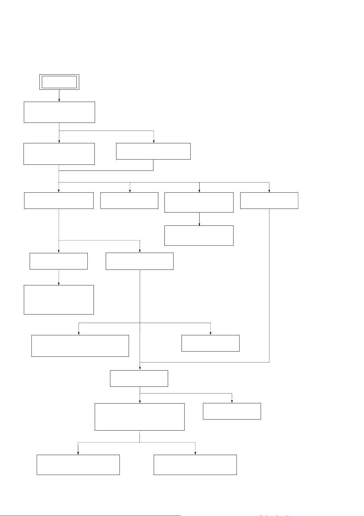
3-1. DISASSEMBLY FLOW
•This set can be disassembled in the order shown below.
SET
3-2. SIDE PANEL (R) ,
SIDE PANEL (L)
(Page 9)
3-3.
TOP PANEL ASSY
(EXCEPT US, CND)
(Page 10)
3-4.
TOP PANEL (US, CND)
SECTION 3
DISASSEMBLY
(Page 10)
3-5.
FRONT PANEL ASSY
(Page 11)
3-8. KEY-LEFT BOARD
(Page 13)
3-9. KEY-RIGHT BOARD,
KEY-CD BOARD,
PANEL BOARD
(Page 13)
3-13. OPTICAL PICK-UP (KSM-213DCP),
BD90 BOARD
(Page 17)
3-10. JACK BOARD
3-12. CD MECHANICAL
(Page 14)
(Page 16)
3-6. MECHANICAL DECK
(EXCEPT US, CND)
(Page 12)
3-7.
BELT (MAIN), BELT (R/F)
(EXCEPT US, CND)
(Page 12)
3-14. BELT (DLM3A)
(Page 18)
3-11. MAIN BOARD
(Page 15)
3-15. CHASSIS
(Page 18)
3-16. PT BOARD (EXCEPT EC55:US),
3-17. LOW-AMP BOARD,
HI-AMP BOARD (EC77/GX99)
(Page 19)
PT (U) BOARD (EC55:US),
POWER TRANSFORMER
(Page 19)
3-18. HI-AMP BOARD (EC55)
(Page 20)
3-19. DC FAN
(Page 20)
8
Page 9
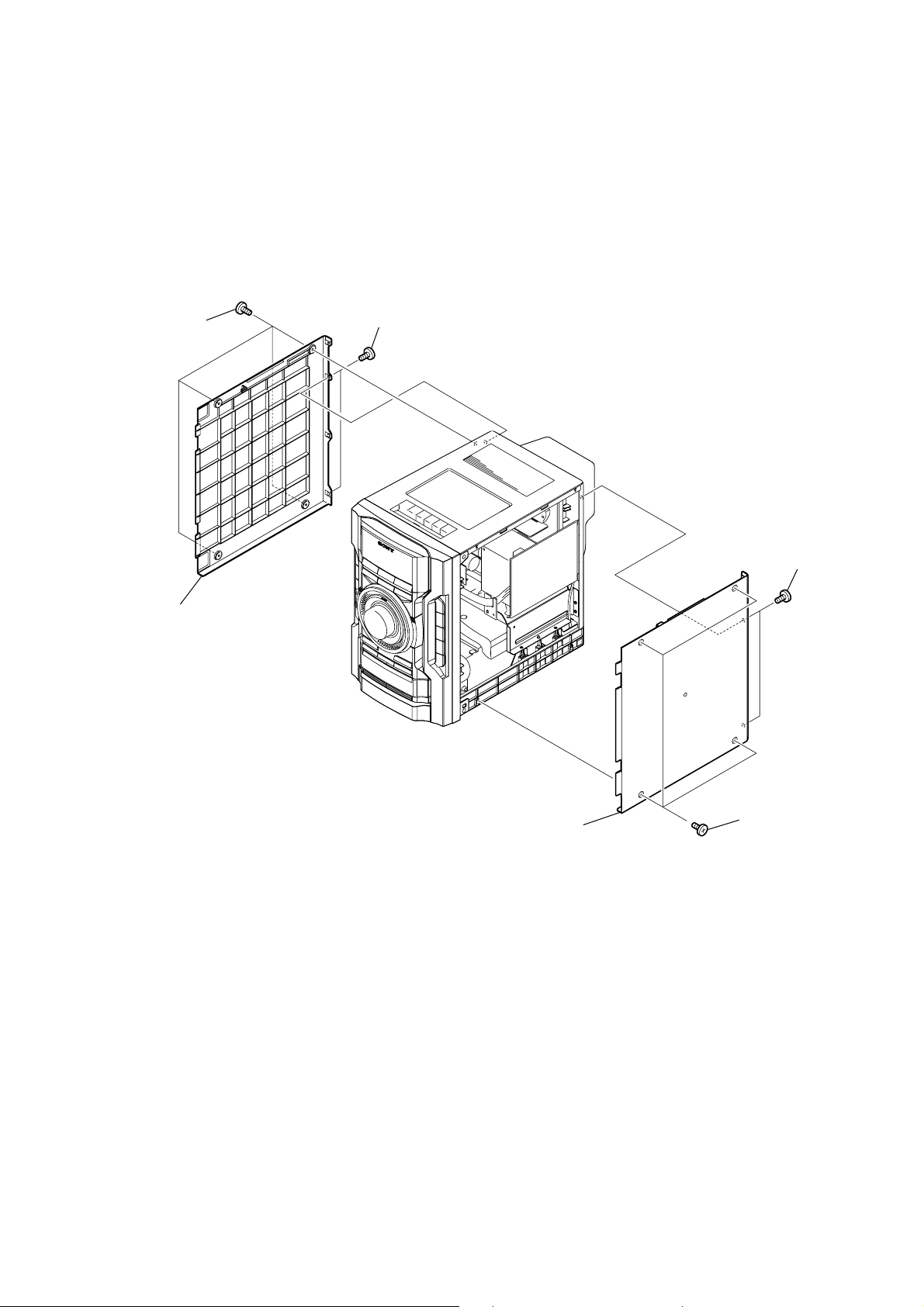
)
Note: Follow the disassembly procedure in the numerical order given.
3-2. SIDE PANEL (R), SIDE PANEL (L)
5
two screws
4
four screws
(TP3
(+BVTP3
×
12
)
×
10
)
HCD-EC55/EC77/GX99
6
side panel (L)
3
side panel (R)
2
1
four screws
(TP3
two screws
(+BVTP3
×
12
)
×
10
9
Page 10
HCD-EC55/EC77/GX99
3-3. TOP PANEL ASSY (EXCEPT US, CND)
6
two
claws
3
two screws
(+BVTP3
5
wire (flat type)
9core (CN606)
×
10
)
2
screw
(+KTP3
×
10
)
7
dowel
4
two screws
(+BVTP3
8
in the direction of the arrow.
×
10
)
Remove the top panel assy
3-4. TOP PANEL (US, CND)
3
two screws
(+BVTP3
2
screw
(+KTP3
×
10
1
screw
(+KTP3
×
10
)
6
dowel
4
5
two
claws
)
×
10
)
two screws
(+BVTP3
7
in the direction of the arrow.
×
10
)
Remove the top panel
10
1
screw
(+KTP3
×
10
)
Page 11

3-5. FRONT PANEL ASSY
1
Turn the bottom rib (not the gear) with a flathead screwdriver in the direction
of arrow A, and draw out the tray in the direction of arrow B.
B
tray
gear
HCD-EC55/EC77/GX99
A
flathead screwdriver
3
door
(CD)
2
two claws
bottom rib
9
front panel
assy
4
fwire (flat type)
27core (CN607)
5
fwire (flat type)
9core (CN605)
8
screw
(+KTP3
×
10
)
7
screw
(+KTP3
×
10
)
6
wire (flat type)
13core (CN302)
11
Page 12
HCD-EC55/EC77/GX99
3-6. MECHANICAL DECK (EXCEPT US, CND)
1
Open the cassette box.
7
Slide the lever in the
direction of the arrow.
2
four screws
(+BVTP 2.6 × 8)
8
mechanical deck
5
(CN501)
6
connector
DECK board
3
two screws
(+BVTP 3 × 6)
3-7. BELT (MAIN), BELT (R/F) (EXCEPT US, CND)
1
belt (MAIN)
4
bracket (DECK)
2
belt (R/F)
12
Page 13
3-8. KEY-LEFT BOARD
9
claw
8
eight screws
(+BVTP 2.6
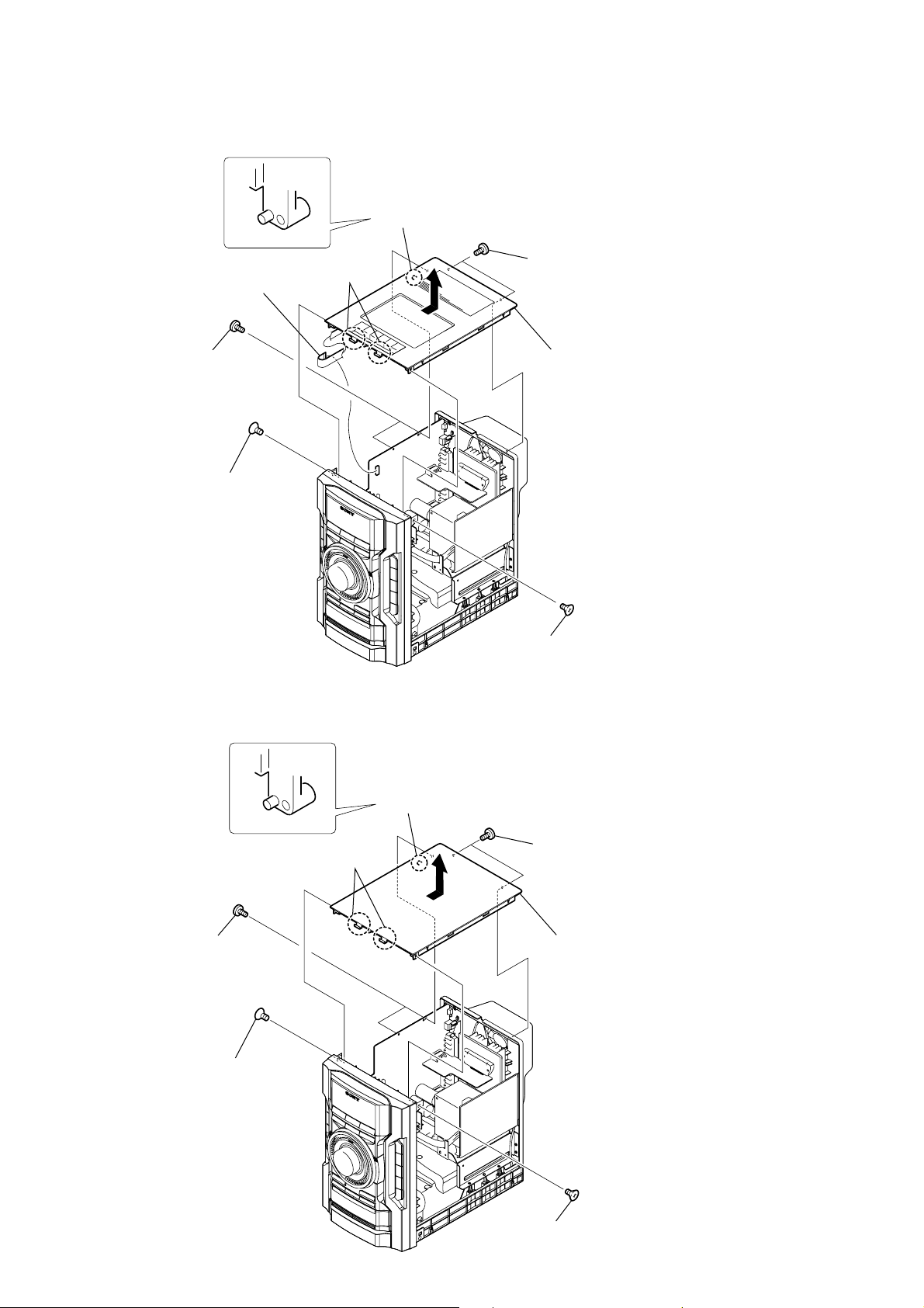
×
8
)
4
six screws
(+BVTP 2.6
×
8
)
6
KEY-CD board
3
KEY-RIGHT board
5
Remove the
soldering.
1
five screws
(+BVTP 2.6
×
8
)
0
wire (flat type)
27core (CN301)
qa
PANEL board
2
connector
(CN403)
7
knob (VOL)
HCD-EC55/EC77/GX99
2
connector
(CN401)
3
KEY-LEFT board
1
four screws
(+BVTP 2.6
×
8
)
3-9. KEY-RIGHT BOARD, KEY-CD BOARD, PANEL BOARD
13
Page 14
HCD-EC55/EC77/GX99
3-10. JACK BOARD
4
JACK board
2
JACK HOLD board
1
three screws
(+BVTP 2.6 × 8)
3
wire (flat type)
9core (CN605)
14
Page 15

3-11. MAIN BOARD
7
two screws
(+BVTP3
×
6
HCD-EC55/EC77/GX99
8
screw
qa
Remove the soldering.
qd
MAIN board
)
(+BVTP3
×
10
)
qs
REG board
3
wire (flat type)
21core (CN608)
4
connector
(CN601)
(EC77/GX99)
6
two screws
(+BVTP3
2
wire (flat type)
27core (CN607)
1
wire (flat type)
9core (CN605)
9
two screws
(+BVTP3
0
×
10
)
5
(CN604)
two screws
(+BVTP3
connector
×
10
)
×
10
)
15
Page 16

HCD-EC55/EC77/GX99
)
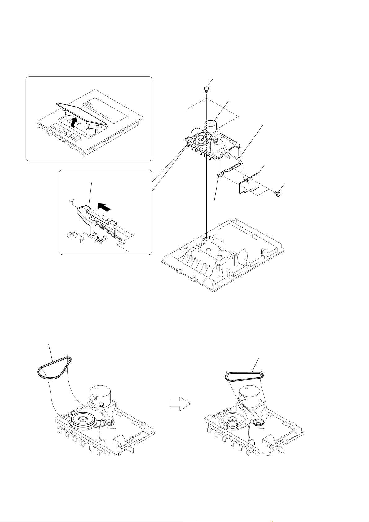
3-12. CD MECHANICAL
1
wire (flat type)
21core (CN608)
3
Remove the CD mechanical in the direction of the arrow.
5
13core
wire (flat type)
2
four screws
(+BVTP3
8
CD mechanical
4
21core
×
10
wire (flat type
)
16
(EC77:US,CND/GX99)
7
6
two tapping screws
(+BVWH 3
cover (DLM3)
×
8
)
Page 17

3-13. OPTICAL PICK-UP (KSM-213DCP), BD90 BOARD
8
Remove the solderings from
the four points.
7
wire (flat type) (16 core)
(CN301)
q;
BD90 board
9
optical pick-up
(KSM-213DCP)
4
two screws
(+PTPWHM 2.6)
1
two screws
(+PTPWHM 2.6)
2
two coil springs (insulator)
3
two insulators
5
two coil springs (insulator)
6
two insulators
HCD-EC55/EC77/GX99
17
Page 18
HCD-EC55/EC77/GX99
3-14. BELT (DLM3A)
5
belt (DLM3A)
1
two screws
2
two screws
4
3
cover
belt (DLM3A)
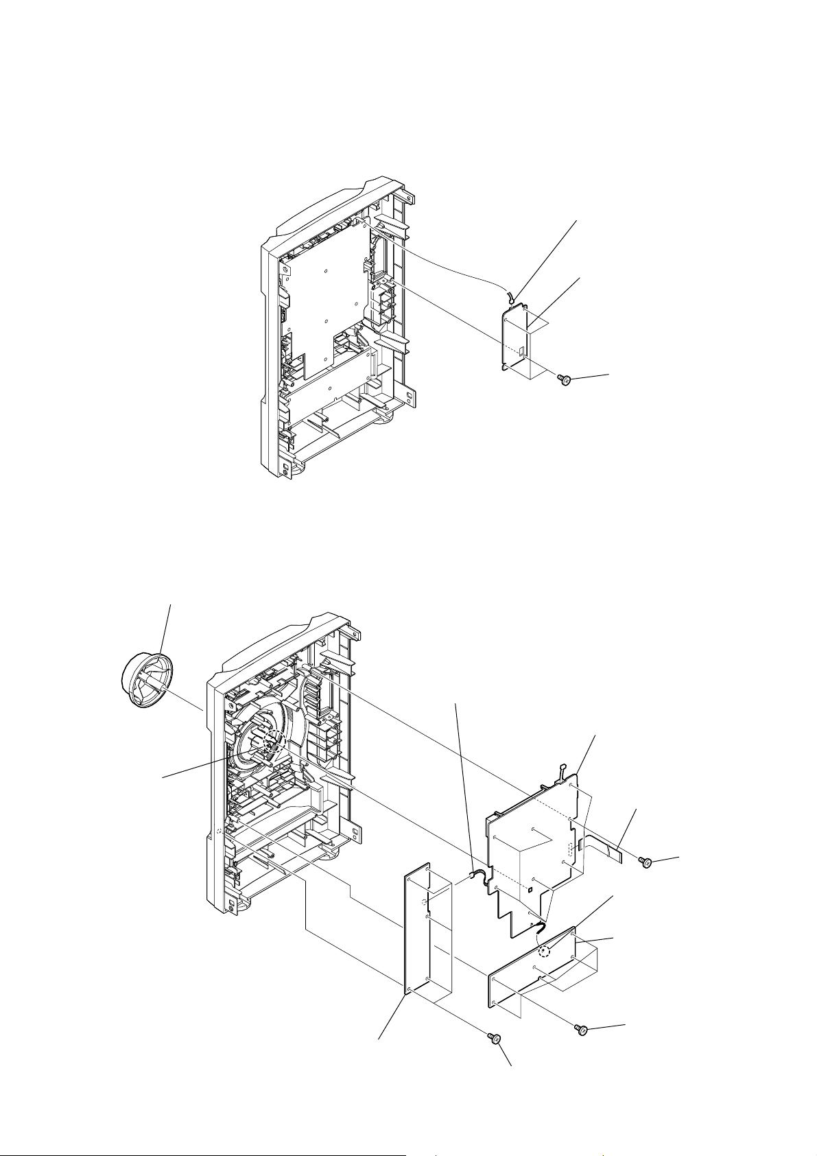
3-15. CHASSIS
5
heatsink support
4
two screws
(+BVTP3
(EC77/GX99)
7
heatsink support
6
two screws
(+BVTP3
qa
×
10
chassis
0
four screws
(+BVTP4
×
10
)
)
×
12
)
1
clamp
qf
POWER cord
qs
screw
(+BVTP3
qd
HOLD board
9
Remove the
solderings.
8
back panel
3
six screws
(+BVTP3
2
two screws
(+BVTP3
Route the harnesses as shown below.
×
10
)
PT board
×
10
×
10
)
)
power cord
groove
18
Page 19
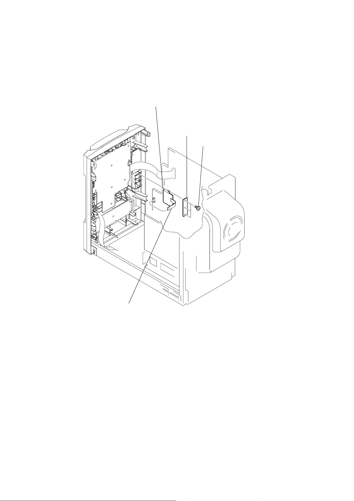
HCD-EC55/EC77/GX99
3-16. PT BOARD (EXCEPT EC55:US), PT (U) BOARD (EC55:US), POWER TRANSFORMER
1
four screws
(+BV4
×
8
)
2
PT (U) board,
power transformer
3-17. LOW-AMP BOARD, HI-AMP BOARD (EC77/GX99)
1
screw
3
HI-AMP board
2
two transisitor
screws
(+BVTP3
×
10
)
2
PT board,
power transformer
(EXCEPT EC55:US)
(EC55:US)
5
two transisitor
screws
4
screw
(+BVTP3
×
10
)
6
LOW-AMP board
19
Page 20
HCD-EC55/EC77/GX99
)
3-18. HI-AMP BOARD (EC55)
1
screw
(+BV3
×
10
)
3-19. DC FAN
2
two transisitor
screws
3
HI-AMP board
1
four screws
(+BVTP3
×
10
20
2
DC fan
Page 21

SECTION 4
TEST MODE
HCD-EC55/EC77/GX99
Ver. 1.1
[MC COLD RESET]
The cold reset clears all data including preset data stored in the
memory to initial conditions. Execute this mode when returning
the set to the customer.
Procedure:
1. In the standby status, press the @/1 button to turn the power
on.
2. Press three buttons of PLAY MODE/TUNING MODE ,
FUNCTION and at last @/1 simultaneously.
3. When “RESET” appears, the machine enters standby status.
[PANEL TEST MODE]
Enter The Panel Test Mode
Procedure:
1. In the standby status, press the @/1 button to turn the power
on.
2. Press three buttons of DISPLAY , x , and TUNER/BAND
simultaneously.
3. When the panel test mode is activated, LEDs and segments of
LCD are all turned on.
Version Check
Procedure:
1. In the panel test mode (all LEDs and segments of LCD are
turned on), press the FUNCTION button.
2. On the LCD, date and version are displayed “xxxxxxxx”.
For example, “0904V014”.
3. From this status, press the TUNER/BAND button, and the
destination is displayed. For example, “ER NA” or “ER E2”
4. To release from this mode, press three buttons of DISPLAY ,
x , and TUNER/BAND simultaneously.
[CD REPEAT 5 LIMIT CANCEL MODE]
Number of repeats for CD playback is 5 times when the repeat mode
is “REPEA T”. This mode enables CD to repeat playback for limitless
times.
Procedure:
1. Press the @/1 button to turn the power on.
2. Press the FUNCTION button to select CD function.
3. Press three buttons of CD u , DSGX , and DISPLAY
simultaneously.
4. It enters the CD repeat 5 limit cancel mode and displays “NO
LIMIT”
5. To release this mode, press the @/1 button to turn the power
off.
[CD SHIP MODE]
This mode can run the CD sled motor optionally. Use this mode, for
instance, when cleaning the optical pick-up.
Procedure:
1. Press the @/1 button to turn the power on.
2. Press the FUNCTION button to select CD function.
3. Press two buttons of CD u and @/1 simultaneously.
4. Set to the CD ship mode. (chucking on)
5. After blink “STANDBY”, “LOCK” is displayed, disconnect
the AC plug.
[CD SLOT LOCK]
This mode is for the antitheft of CD disc in shop. (not for transport)
Procedure:
1. Press the @/1 button to turn the power on.
2. Press the FUNCTION button to select CD function.
3. Insert a disc.
4. While pressing the x button, press the Z button for more 5
seconds.
5. The message “LOCKED” is displayed and the disc slot is
locked. (Even if exiting from this mode, the disc slot is still
locked)
6. If press the Z button to eject the disc, the message
“LOCKED” is displayed and can not eject the disc.
7. To release this lock, while pressing the x button, press the
Z button for 5 seconds again.
8. The message “UNLOCKED” is displayed and the disc slot is
unlocked.
[CD POWER MANAGE]
This mode is for switch the CD power supply on/off. Even if this
state pulls out AC plug, it is held.
Procedure:
1. Press the @/1 button to turn the power on.
2. Press the FUNCTION button to select CD function.
3. Press the @/1 button again to turn the power off (standby).
4. After pressing the DISPLAY button, while pressing the x
button, press the @/1 button.
5. It turns power on and display “CD POWER”, then display
“ON” or “OFF”.
[CHANGE-OVER THE AM TUNING INTERVAL]
(Except European and Russian models)
The AM tuning interval can be changed over 9 kHz or 10 kHz.
Procedure:
1. Press the @/1 button to turn the power on.
2. Press the TUNER/BAND button to select TUNER (AM)
function.
3. Press the @/1 button again to turn the power off (standby).
4. After pressing the DISPLAY button, while pressing the
TUNING+
5. It turns power on and display “9k STEP” or “10k STEP”, and
thus the tuning interval is changed over.
ML
button, press the @/1 button.
[CD SHIP AND COLD RESET]
Procedure:
1. Press the @/1 button to turn the power on.
2. Press the FUNCTION button to select CD function.
3. Press three buttons of PLAY MODE/TUNING MODE ,
CD u and @/1 simultaneously.
4. After blink “STANDBY”, “RESET” is displayed, disconnect
the AC plug.
21
Page 22

HCD-EC55/EC77/GX99
[CD SERVO TEST MODE]
This mode can check the servo system operations of the optical
pick-up system (= optical unit + BD board).
Note1: Do not enter the [CD SERVO TEST MODE] while any other test
mode is in progress.
Note2: Do not enter any other test mode while the [CD SERVO TEST
MODE] is in progress.
How to Enter the CD Servo Test Mode
Procedure:
1. Press the @/1 button to turn the power on.
2. Press the FUNCTION button to select CD function.
3.
Press three buttons of CD u , PLAY MODE/TUNING MODE
and DISPLAY simultaneously.
4. It enters the CD servo test mode and displays “BDT S CU”.
How to Exit from the CD Servo Test Mode
Procedure:
1. Press three buttons of CD u , PLA Y MODE/TUNING MODE
and DISPLAY simultaneously.
2. It exits from the CD Servo Test Mode and returns to the
ordinary CD function.
Key Operation:
+ , – : Use these keys to move between the five modes
contained in the CD Servo Test Mode, that are the
S-Curve Mode, the RAM Read Mode, the RAM
Write Mode, the Command Out Mode and the Error
Rate Mode as described below . Also, use these keys
to move between the menus within the respective
five modes. When + is pressed, the screen
advances to the next menu or to the next mode. When
– is pressed, the screen returns back to the
previous menu or to the previous mode. Use these
keys also to increase or decrease the numeric value
when changing the numeric value. Pressing +
increases the value and pressing – decreases the
value.
DSGX , EQ :Use these keys to move between the different layers
of the hierarchy of the CD Servo Test Mode shown
below. Press DSGX to move down to the lower
layer, and press EQ to move up to the higher layer.
TUNING+
FUNCTION :Use this key to execute Command Out in the
ML
,
lm
–TUNING :
Use these keys to move the cursor to the right digit
or to the left digit in the six-digit number, when
changing the numeric value.
Press TUNING+
the right, and press
ML
lm
to move the cursor to
–TUNING to return
the cursor to the left.
Command Out Mode.
CD Servo Test Mode Tree:
S Curve Mode LD ON
(BDT S CU) (LD ON)
RAM Read Mode
(BDTRAM R) (DISCTYPE) (0000)
Gain Index value indication
(GAININDX) (0001)
RFO GAIN value indication
(RFO_GAIN) (0009)
FEO GAIN value indication
(FEO_GAIN) (0005)
SBAD GAIN value indication
(SBAD_GAI) (0007)
TEO GAIN value indication
(TEO_GAIN) (0000)
Disc Size value indication
(DISCSIZE) (0000)
(OPABRKER) (0000)
SBBT Data value indication
(SBBT DAT) (006B)
FEOOCD value indication
(FEOOCD) (F780)
RAM Write Mode
(BDTRAM W) (00 SPG) (Non mask:00, Mask:01)
Fix RF Gain value edit
(00 FIX) (Non Fix:00, AL Fix:01, RW Fix:02)
TMAX ON value edit
(00 TMA)
Driver Mute OFF value edit
(00 D_M) (Normal:00, Forced OFF:01)
Command Out Mode
(BDT COMO) (COMOUT6X) (000000) (OK)
READ2X value edit command out
(READ2X) (60) (50)
REG READ value edit command out
(REG_READ) (00) (0000)
FEBC? command out
(FEBC?) (00)
FGADD? command out
(FGADD?) (10)
TEBC? command out
(TEBC?) (00)
TGADD? command out
(TGADD?) (00)
RFGC? command out
(RFGC?) (00)
FEOF? command out
(FEOF?) (FFC0)
TEOF? command out
(TEOF?) (FFC0)
TEIOCD1? command out
(TEIOCD1?) (FE80)
TEIOCD2? command out
(TEIOCD2?) (FF40)
TEIOCD3? command out
(TEIOCD3?) (FFC0)
TEOOCD? command out
(TEOOCD?) (FD00)
FEOOCD? command out
(FEOOCD?) (F780)
MONITOR value edit command out
(MONITOR) (570A00) (OK)
Error Rate Mode Error rate indication
(BDT ERR) (00000000)
Higher layer Lower layer of menu hierarchy
Disc Type value indication
Op ABRAKE Error
SPG Mask value edit
COMOUT6X value edit command out
value indication
22
Page 23

HCD-EC55/EC77/GX99
[CD SERVICE MODE]
This mode can move the SLED of the optical pick-up, and also can
turn the optical pick-up laser power on and off.
Procedure:
1. Press the @/1 button to turn the power on.
2. Press three buttons of CD u ,
simultaneously.
4. It enters the CD service mode and displays “SERVICE”.
5. To exit from this mode, press three buttons of CD u ,
and DISPLAY simultaneously.
Key Operation:
TUNING+
PLAY MODE/TUNING MODE :
ML
,
lm
Use these keys to move the SLED. When
TUNING+
SLED moves to outer circumference and the message
“SLED OUT” is displayed.
When
lm
the SLED moves to inner circumference and the
message “SLED IN” is displayed.
Use this key to turn the optical pick-up laser power
on and off. When the laser power is turned on, the
message “LD ON” is displayed. When the laser
power is turned off, the message “LD OFF” is
displayed.
–TUNING :
ML
is pressed in this mode, the
–TUNING is pressed in this mode,
+ , and DISPLAY
[CD ERROR CODE]
The past errors of the CD mechanism (CDM) are displayed as the
CDM Errors, and those of the optical pick-up system (= optical unit
+ BD board) are displayed as the BD Errors as shown below.
Procedure:
1. Press the @/1 button to turn the power on.
2. Press the FUNCTION button to select CD function.
3. Press three buttons of CD u , x and DISPLAY
simultaneously.
4. Then, the CDM error code is displayed as “M0xxxxxx” (x
means hexadecimal number) on the LCD screen as shown
below.
5. Every pressing of the TUNING+
increments the number after “M” starting from “M0” up to
“M9”, and then returns to “M0”. Every pressing of the
lm
number after “M”. The smaller the error code number is, the
newer the error content is.
6. When the PLAY MODE/TUNING MODE b utton is pressed
then, the BD error code is displayed as “D0xxxxxx” (x means
hexadecimal number) on the LCD screen as shown below. In
the same way as the CDM error code, use of the
TUNING+
this mode enables tracing of the error history.
7. To exit from this mode, press the @/1 button to turn the
power off.
–TUNING button in this mode decrements the
ML
and the
ML
lm
button in this mode
–TUNING buttons in
Contents of “CDM Errors”
Error display example
M
0 FF 11 42
1 234
1 It indicates the error history number
0 to 9: The error code number 0 indicates the newest error.
+
2 It indicates whether the CDM error occurs in the normal
operations or during the initialization operation.
FF : The error has occurred in the normal
Other than FF : The error has occurred during the initialization
3 It indicates the processing during which the trouble has
occurred.
01: The disc EJECT processing is in progress.
02: The disc INSERTION-WAITING processing is in
progress.
03: Processing of the disc INSERTION-REQUEST for the
upper CD tray is in progress.
04: Processing of the disc EJECTION-REQUEST for the
upper CD tray is in progress.
05: The disc pulling-in operation is in progress.
06: The disc chucking processing is in progress.
07: The disc re-chucking processing is in progress.
08: The disc chucking-release completion operation is in
progress.
4 It indicates the operation during which the trouble has occurred.
00 : Waiting for the operation.
10 to 13 : The disc EJECT operation is in progress.
20 : The disc pulling-in operation is in progress.
30 : The disc chucking-release operation is in progress.
40 to 43 : The disc EJECT operation due to error is in progress.
Contents of “BD Errors”
Error display example
D 0 02 09 01
1 234
1 It indicates the error history number
0 to 9: The error code number 0 indicates the newest error.
2 It indicates the error content
01: The focus servo cannot lock-in.
02: GFS is no good (NG).
03: The startup time exceeds the specified period of time (time
over)
04: The focus servo is unlocked continuously.
05: Q code cannot be obtained within the specified period of
time.
06: The tracking servo cannot lock-in.
07: Blank disc
operations.
operation.
23
Page 24

HCD-EC55/EC77/GX99
3 It indicates the on-going processing of optical pick-up system
(= optical unit + BD board) when the trouble has occurred.
01: The CD SHIP mode processing is in progress.
02: The POWER OFF processing is in progress.
03: The INITIALIZE processing is in progress.
04: The optical pick-up system (= optical unit + BD board)
is in the stop state.
05: The STOP operation is in progress.
06: The startup processing is in progress.
07: The TOC read-in processing is in progress.
08: The SEARCH operation is in progress.
09: The PLAY operation is in progress.
0A: The PAUSE operation is in progress.
0B: The PLAY – MANUAL SEARCH operation is in
progress.
0C: The PAUSE – MANUAL SEARCH operation is in
progress.
4 It indicates the operation that is being processed when the
trouble has occurred.
It indicates the step number of each processing specified by
3. Because the numbers of steps are different in each
processing, this number is different in each processing.
24
Page 25

Screw
position
L-CH
peak
within
1dB
Output
level
L-CH
peak
R-CH
peak
within
1dB
Screw
position
R-CH
peak
set
JACK board
PHONES jack
(J402)
+
–
level meter
test tape
P-4-A063
(6.3 kHz, −10 dB)
SECTION 5
MECHANICAL ADJUSTMENTS
HCD-EC55/EC77/GX99
SECTION 6
ELECTRICAL ADJUSTMENTS
• Precaution
1. Clean the following parts with a denatured-alcohol-moistened
swab :
record/playback head pinch roller
erase head rubber belts
capstan idlers
2. Demagnetize the record/playback head with a head
demagnetizer. (Do not bring the head magnetizer close to the
erase head.)
3. Do not use a magnetized screwdriver for the adjustments.
4. After the adjustments, appiy suitable locking compound to
the parts adjusted.
5. The adjustments should be performed with the rated power
supply voltage unless otherwise noted.
• Torque Measurement
Mode
FWD
FWD
back tension
FF
REW
Torque meter
CQ-102AS
CQ-102C
CQ-201AS
CQ-201B
Meter reading
2.0 – 8.0 mN • m
(20 to 80 g • cm)
(0.28 – 1.12 oz • inch)
0.15 – 0.6 mN • m
(1.5 to 6 g • cm)
(0.021 – 0.083 oz • inch)
5 – 17.7 mN • m
(50 to 177 g • cm)
(0.7 – 2.48 oz • inch)
5 – 17.7 mN • m
(50 to 177 g • cm)
(0.7 – 2.48 oz • inch)
• Tape T ension Measurement
Mode Tension Meter Meter Reading
FWD CQ-403A
more than 80 g
(more than 2.82 oz)
DECK SECTION (EXCEPT US, CND)
0 dB=0.775 V
1. Demagnetize the record/playback head with a head
demagnetizer.
2. Do not use a magnetized screwdriver for the adjustments.
• Test T ape
Tape Signal Used for
P-4-A063 6.3 kHz, -10 dB Azimuth Adjustment
RECORD/PLA YBA CK HEAD AZIMUTH ADJUSTMENT
Procedure:
1. Mode: Playback
2. Turn the adjustment screw and check output peaks. If the peaks
do not match for L-CH and R-CH, turn the adjustment screw
so that outputs match within 1dB of peak.
3. Mode: Playback
test tape
P-4-A063
(6.3 kHz, −10 dB)
in phase 45° 90° 135° 180°
4. After the adjustments, apply suitable locking compound to
JACK board
PHONES jack
(J402)
set
waveform of oscilloscope
good
oscilloscope
V
wrong
H
the pats adjusted.
25
Page 26
HCD-EC55/EC77/GX99
Adjustment Location: Record/Playback/Erase Head
CD SECTION
Note:
1. CD Block is basically constructed to operate without adjustment.
2. Use YEDS-18 disc (3-702-101-01) unless otherwise indicated.
3. Use an oscilloscope with more than 10 MΩ impedance.
4. Clean the object lens by an applicator with neutral detergent when the
signal level is low than specified value with the following checks.
5. Check the focus bias check when optical pick-up block is replaced.
FOCUS BIAS CHECK
oscilloscope
(DC range)
BD90 board
TP (RFI)
TP (VC)
Procedure :
1. Connect oscilloscope to TP (RFI) and TP (VC) on the BD90
board.
2. Press the I/1 button to turn the power ON, and press
the Z (CD) button to open the CD disc tray.
3. Set disc (YEDS-18) on the tray and press the CD u button
to playback.
4. Confirm that oscilloscope waveform is as shown in the figure
below. (eye pattern)
A good eye pattern means that the diamond shape (◊) in the
center of the waveform can be clearly distinguished.
+
–
Checking Location:
– BD90 Board (Side B) –
TP
(VC)
TP
(RFI)
IC101
VOLT/DIV: 200 mV
TIME/DIV: 500 ns
level:
0.5 to 0.8 Vp-p
26
Page 27

HCD-EC55/EC77/GX99
r
FM RF signal
generator
Carrier frequency: 98MHz
Modulation:
deviation by FM 75 kHz
Output level: 60 dBuV
+
–
level meter
MAIN board
TP(TUNER-GND)
MAIN board
IC801 pin qs
(TUNER OUT L-ch)
set
MAIN board
ANTENNA
CN801 pin 2
MAIN board
ANTENNA
CN801 pin 3
Ver. 1.1
TUNER SECTION 0 dB=1 µV
[AM]
Setting:
FUNCTION: TUNER
TUNER/BAND button: AM
60 cm
loop antenna A
AM RF signal
generator
30% amplitude
modulation by
400 Hz signal
Output level: 54 dBuV
[FM]
Setting:
FUNCTION: TUNER
TUNER/BAND button: FM
FM RF signal
generator
0.01 µF
75kHz frequency
deviation by 1K Hz
signal
Output level: as low as possible
(8dBuV)
loop antenna B
set
MAIN board
ANTENNA
CN801 pin 12
MAIN board
ANTENNA
CN801 pin 3
set
MAIN board
ANTENNA
CN801 pin 2
level mete
32 Ω
JACK board
PHONES jack (J402)
32 Ω
JACK board
PHONES jack (J402)
+
–
level meter
+
–
AM FREQUENCY COVERAGE ADJUSTMENT
(US, Canadian, Australian models)
Adjustment Part Frequency Display Reading on Digital Voltmeter
L801 530 kHz 1.5 ± 0.1 V
Confirmation 1,710 kHz 8 ± 0.5 V
AM FREQUENCY COVERAGE ADJUSTMENT (Other models)
Adjustment Part Frequency Display Reading on Digital Voltmeter
L801 531 kHz 1.5 ± 0.1 V
Confirmation 1,602 kHz 7.2 ± 0.5 V
AM TRACKING ADJUSTMENT (US, Canadian, Australian models)
Adjust for a maximum reading on level meter
L805 530 kHz
AM TRACKING ADJUSTMENT (Other models)
Adjust for a maximum reading on level meter
L805 531 kHz
FM FREQUENCY COVERAGE ADJUSTMENT
Adjustment Part Frequency Display Reading on Digital Voltmeter
L803 87.5 kHz 1.75 ± 0.1 V
Confirmation 108 kHz 6.2 ± 0.5 V
FM TRACKING ADJUSTMENT
Adjust for a maximum reading on level meter
L804 98 MHz
Adjustment Location: MAIN board (See page 28).
digital voltmeter
MAIN board
TP (TUNER VT)
100 kΩ
•Repeat the procedures in each adjustment several times.
[FM DETECTOR ADJUSTMENT]
Setting:
FUNCTION: TUNER
TUNER/BAND button: FM
1. Tune the set to 98 MHz.
2. Adjust L802 so that modulation distortion may become the
best in the vicinity of the maximum value where the tuner out
level becomes –15dBuV or more.
27
Page 28

HCD-EC55/EC77/GX99
[FM Auto Stop Check]
generator
SET
+
75 Ω
Procedure:
1. Turn the power on.
2. Input the following signal from Signal Generator to FM
antenna input directly.
* Carrier Freq: A = 87.5 MHz, B = 98 MHz, C = 108 MHz
Deviation : 75 kHz
Modulation : 1 kHz
ANT input : 35 dBu (EMF)
Note: Please use 75 ohm “coaxial cable” to connect SG and the set. You
cannot use video cable for checking.
Please use SG whose output impedance is 75 ohm.
3. Set to FM tuner function and scan the input FM signal with
automatic scanning.
4. Confirm that input Frequency of A, B and C are detected and
automatic scanning stops.
The stop of automatic scanning means “The station signal is received
in good condition.”
Adjustment Location and Connecting Points
– MAIN BOARD (Component Side) –
AM Tracking
Adjustment
FM Frequency
L803
Coverage Adjustment
AM Frequency
Coverage Adjustment
JW801
FM Detector
L802
Adjustment
– MAIN BOARD (Conductor Side) –
CN801
3
FM
ANTENNA
1
AM
L805
L801
CN801
ANTENNA
L804
FM Tracking
Adjustment
3
FM
1
AM
IC801 pin wk
(TUNER VT)
28
36
IC801
1
12
IC801 pin qs
(TUNER OUT L-ch)
JW801
19
18
TUNER-GND
28
Page 29

SECTION 7
DIAGRAMS
HCD-EC55/EC77/GX99
Ver. 1.1
THIS NOTE IS COMMON FOR PRINTED WIRING BOARDS AND SCHEMATIC DIAGRAMS.
(In addition to this, the necessary note is printed in each block.)
Note on Schematic Diagram:
• All capacitors are in µF unless otherwise noted. (p: pF)
50 WV or less are not indicated except f or electrolytics and
tantalums.
• All resistors are in Ω and
specified.
• f : internal component.
• 2 : nonflammable resistor.
• 5 : fusible resistor.
• C : panel designation.
Note:
The components identified by mark 0 or dotted line with mark 0 are
critical for safety.
Replace only with part
number specified.
• H : adjustment for repair.
• A : B+ Line.
• B : B– Line.
•Voltages are taken with a VOM (Input impedance 10 MΩ).
Voltage variations may be noted due to normal production
tolerances.
•Waveforms are taken with a oscilloscope.
Voltage variations may be noted due to normal production
tolerances.
– HI-AMP/LOW-AMP Section –
No mark: CD STOP
– DECK Section –
No mark: TAPE PLAY or TAPE REC
– Other Section –
No mark: CD PLAY
• Circled numbers refer to waveforms.
• Signal path.
F : TUNER (FM)
J : TUNER (AM)
f : CD
d : AUDIO
E : PB (TAPE)
a : REC (TAPE)
•Abbreviation
AR : Argentine model
AUS: Australian model
CND : Canadian model
E2 : 120 V AC area in E model
E3 : 240 V AC area in E model
E51 : Chilean and Peruvian models
KR : Korean model
MX : Mexican model
RU : Russian model
SP : Singapore model
1
4
/
W or less unless otherwise
Note:
Les composants identifiés
par une marque 0 sont critiques pour la sécurité.
Ne les remplacer que par une
piéce portant le numéro
spécifié.
Note on Printed Wiring Boards:
• X : parts extracted from the component side.
• Y : parts extracted from the conductor side.
• f : internal component.
•
• Indication of transistor.
: Pattern from the side which enables seeing.
Caution:
Pattern face side: Parts on the pattern face side seen from
(Side B) the pattern face are indicated.
Parts face side: Parts on the parts face side seen from
(Side A) the parts face are indicated.
C
Q
B
E
B
These are omitted.
Q
CE
These are omitted.
• Circuit Boards Location
EC77/GX99
KEY-LEFT board
REG board
JACK board
EC55
KEY-LEFT board
DECK board (EXCEPT US, CND)
PANEL board
KEY-CD board
DECK board (EXCEPT US)
PANEL board
HI-AMP board
MAIN board
LOW-AMP board
PT board
BD90 board
KEY-RIGHT board
HI-AMP board
MAIN board
PT board (EXCEPT US)
HCD-EC55/EC77/GX99
PT (U) board (US)
REG board
JACK board
BD90 board
KEY-CD board
KEY-RIGHT board
2929
Page 30

HCD-EC55/EC77/GX99
7-1. BLOCK DIAGRAM — BD/DRIVER SECTION —
OPTICAL PICK-UP
BLOCK
(KSM-213DCP)
DETECTOR
VCC
FOCUS
COIL
TRACKING
COIL
M401
(SPINDLE)
M402
(SLED)
15
16
VC
12
A
11
B
10
C
13
D
14
E
F
LD
GND
PD
VR
F+
F
T+
T
SP+
M
SP
SL+
+1.7V
+3.3V
95
FN11(A)
97
FP11(B)
94
FN12(C)
96
FP12(D)
100
9
Q301
AUTOMATIC
7
8
5
6
4
1
3
2
POWER
CONTROLLER
IC401
SL/SP MOTOR
DRIVER
FOCUS/TRACKING
COIL DRIVER
26
VD4+
27
VD4-
18
VD3+
17
VD3-
2
VO1+
1
VO1-
12
VO2-
IN1
IN2'
IN3'
BIAS
IN4'
3
9
20
23
24
X102
16.934MHz
+3.3V
S201
(LIMIT)
98
91
24
23
42
20
13
12
10
11
9
TN1(E)
TP1(F)
LDo
XO
XI
MD1
IOO(/MSO)
DMO
FMO
TRo
VREF
F0o
M
11
SL
VO2+
MUTE
21
7
I01(/UHS0)
IC101
RF AMP,DSP,MP3
BUCK(CLK)
BUS0
BUS1
BUS2
BUS3
RST
CCE
P100
SBSY
ZDET
RO
SYSTEM CONTROLLER
IC301
(1/2)
CD MECHANISM DECK
IC201
+1.5V
38
39
40
41
42
37
43
48
54
58
30
LO
27
I/O-BUS0
I/O-BUS1
I/O-BUS2
I/O-BUS3
O-CD-BUCK
O-CD-RST
O-CD-CCE
O-CD-REQ
O-CD-SBSY
I-CD-ZDET
5 1
CD-L
CD-R
+1.8
REG
3
A
+
I/O-BUS0
I/O-BUS1
I/O-BUS2
I/O-BUS3
O-CD-BUCK
O-CD-CCE
O-CD-REQ
O-CD-SBSY
O-CD-M-MUTE
I-CD-ZDET
O-CD-RST
MAIN
SECTION
(Page 32)
3.3V
17
I/O-CD-BUS0
18
I/O-CD-BUS1
19
I/O-CD-BUS2
20
I/O-CD-BUS3
25
O-CD-BUCK
26
O-CD-CCE
31
O-CD-REQ
43
O-CD-SBSY
30
O-CD-M-MUTE
29
I-CD-ZDET
27
O-CD-RST
I-MODEL
46
I-CD-SW3
I-CD-SW1
I-CD-CHACK
I-CD-SW2
I-CD-CLOSE
I-CD-STOCK
I-CD-OPEN
O-CD-M1+
O-CD-M1-
O-CD-M2+
O-CD-M2-
I-SUFFIX
5
7
21
6
22
23
24
8
10
11
12
47
AVCC
I-SW3
I-SW1
I-CHACK
I-SW2
I-CLOSE
I-STOCK
I-OPEN
Q313,318
Q314,317
Q311,316
Q312,315
Q307-310
CONTROLLER
MOTOR
DRIVER
MOTOR
DRIVER
MOTOR
DRIVER
MOTOR
DRIVER
CD
MOTOR
+
M
-
+
M
-
V-STBY
• Signal Path
HCD-EC55/EC77/GX99
M-MUTE
: CD
3030
Page 31

7-2. BLOCK DIAGRAM — TUNER SECTION —
AM TRACKING
D801
FL803
ANTENNA
FM/AM
CN801
1
3
AM
FM
FM TRACKING
L804
FM RF
BPF
L805
D804
L801
AM OSC
AM FREQUENCY
COVERAGE
1
31
36
34
AM RF-IN
AM-OSC
FM RF-IN
FM RF-OUT
AM-MIX
FM-MIX
IF TRANSFORMER
T801
5
FL802
10.7MHz
CF801
450kHz
Q803
IF AMP
AM/FM ,DET,OSC
MIX, PLL ,IF AMP
AM IF-IN
7
FM IF-IN
83
IC801
FM-DET
11
FM DETECTOR
L802
L-OUT
R-OUT
HCD-EC55/EC77/GX99
TUNER
12
13
L-CH
TUNER
R-CH
L-CH
R-CH
D803
L803
FM OSC
FM FREQUENCY
COVERAGE
26
27
28
PD
LP-IN
LP-OUT
32
FM-OSC
XIN
19 20
X801
75kHz
XOUT
AGC
Q801
+3V
25
18
DO
16
DI
17
CL
15
CE
TU-ANSD
+5V
TU-DO
TU-DI
TU-CLK
TU-CE
+3V
REG
Q802
+5V
REG
VM9V
TU-ANSD
TU-DO
TU-CE
TU-DI
TU-CLK
+9V
B
MAIN
SECTION
(Page 32)
• Signal Path
: TUNER(FM)
: TUNER(AM)
HCD-EC55/EC77/GX99
3131
Page 32

HCD-EC55/EC77/GX99
Ver. 1.1
7-3. BLOCK DIAGRAM — MAIN SECTION —
J401
AUDIO IN
B
TUNER
SECTION
(Page 31)
A
BD/DRIVER
SECTION
(Page 30)
EXCEPT US,CND
TAPE MECHANISM DECK
BLOCK
L-CH
REC/PB
HEAD
R-CH
P-SW
M
M-SW
+9V
L-CH
R-CH
TU-DO
TU-DI
TU-CLK
TU-CE
TU-ANSD
CD-L
CD-R
R-CH
+9V
R-CH
VM9V
R-CH
R-CH
S501(1/2)
L501
BIAS OSC
(REC/PB)
S501(2/2)
(REC/PB)
BIAS
OSC
Q501
Q502
IC501
75
5
HEAD AMP
IC502
+ 4 V
TONE CONTROLLER
AUDIO-L
5 27
6
TUNER-L
4
TAPE-L
CD-L
7
5
HEAD AMP
7
AUDIO SELECTOR
IC602
L-OUT
R-OUT
CLK
DATA
REC-L
D303
VOLUME
26
21
22
8
SW303-
FUCTION
KEY
SW311-318
FUCTION
KEY
SW301,302
FUCTION
KEY
LED302
STANDBY
LED301
(BACK RIGHT)
µCON +B
Q304,305
RESET
VOLUME
LIQUID CRYSTAL
R-CH
310
CONTROL
RECEIVER
S301
DISPLAY
IC302
REMOTE
LCD301
32.768kHz
Q301
LED
DRIVE
2
31
X301
X302
5MHz
Q306
RESET
SWITCH
SYSTEM CONTROLLER
3
O-FUNC-CLK
4
O-FUNC-DATA
33
I-TU-DO
57
O-TU-DI
56
O-TU-CLK
O-TU-CE
55
39
I-TU-ANSD
14
X1A
13
X0A
93
X0
92
X1
40
I-TP-STATE
37
I-KEY1
38
I-KEY2
41
I-KEY-WAKE
28
O-LED-STBY
45
O-LED
I-RMC
9
42
I-HOLD
54
RESET
48
I-RE-VOL
63
.
64
.
67
SEG0
89
SEG31
.
94
100
COM0
59
COM3
62
IC301(2/2)
O-POWER
O-CD-ON
I-P-MONI
IC101
IC102
POWER
AMP
(HIGH)
13
AMP
CONTROL
5
VM9V
11
IC101
IC102
POWER
AMP
(LOW)
13
D617
POWER
MONITOR
Q618
+8.5V
D616
Q151
OVERLOAD
DET
R-CH
5
Q151
OVERLOAD
DET
R-CH
D602
Q302,303
AVDD
( +3.3V)
DVDD
( +3.3V)
VM+7V
+8.5V
REG
Q101,102
AMP
PROTECT
D619,620
+3.3V
REG
Q191
+3.3V
REG
Q624
POWER
RELAY
Q101,102
AMP
PROTECT
Q603
CURRENT
DET
Q605,606
PROTECT
DET
3
Q619
DRIVE
IC601
+9V
REG
D055(2/2)
Q604
SP RELAY
DRIVER
+9V
D602
D606
D607,609
+VP
-VP
D611,612
1
RY001:EXCEPT E2,E3,E51,MX,KR,AR,SP,AUS
RY002:E2,E3,E51,MX,KR,AR,SP,AUS
D055(1/2)
D051,052
11
Q608
Q622
49
36
CD POWER
CONTROLLER
1
RY601
RY602
D601
Q601,602
CONTROL
TRANSFORMER
R-CH
R-CH
R-CH
FAN
TP002 : EC77/GX99
TP003 : EC55
POWER
TRANSFORMER
(MAIN)
TP001
POWER
(SUB)
M
TB601
J601
M901
FAN MOTOR
S001
J402
PHONES
L
SPEAKER
HIGH FREQ.
IMPEDANCE:
USE 8
R
SUBW00FER
OUT
TB602
EC77/GX99 EC55
L
SPEAKER
LOW FREQ.
IMPEDANCE:
USE 8
R
E2,E3,E51,SP
VOLTAGE
SELECTOR
AC
EC77/GX99
GX99
SPEAKER
IMPEDANCE:
USE 6
• R-CH is omitted due to same as L-CH.
• Signal Path
: TUNER(FM)
: TUNER(AM)
: CD
: AUDIO
: PB (TAPE)
: REC (TAPE)
IN
HCD-EC55/EC77/GX99
3232
Page 33

7-4. PRINTED WIRING BOARD — BD90 BOARD —
HCD-EC55/EC77/GX99
Ver. 1.1
• See page 29 for Circuit Boards Location. :Uses unleaded solder.
1
2 3 4 5 6 7 8 9 10 11 12
A
BD90 BOARD (SIDE B)
BD90 BOARD (SIDE A)
B
C401
C405
C
D
R212
R211
E
C207
IC201
5
1
C206
3
4
C201
R201
C205
F
C202
C204
X102
C115
R112
R111
C133
R155
C130
C128
C309
Q301
C106
C306
R303
R302
E
C307
R304
R301
TP121
RFI
C123
R151
C149
C122
C144
C148
VC
R143
C143
C140
C141
R140
C138
C124
C139
R144
R148
R142
C137
C142
C146
C150
C125
R136
R135
C147
R146
B8
C145
R134
C105
C104
C118
R139
R130
C100
R145
R147
R149
R150
R129
C117
CN301
R128
C136
R126
R125
C107
C120
M
R127
C112
IC101
C101
C119
C153
R114
C102
C126
C127
R118
C113
M401
(SPINDLE)
R402
C103
R101
C303
R120
R102
C108
C301
C302
R104
R106
R105
R415
R414
R113
R154
C132
S201
(LIMIT)
C109
IC401
R110
C110
R153
C116
C403
R405
M402
(SLED)
B7
C404
M
R210
R209
R218
R219
R220
R221
R222
R223
R408
R157
R156
R108
R208
R207
R206
R205
R204
R203
C151
C152
R202
MAIN BOARD
CN201
A
SUFFIX-12
(
Page 35
CN608
(
SUFFIX-13
SUPPLEMENT-1
(
Page 3
(
B9
G
HCD-EC55/EC77/GX99
OPTICAL PICK-UP BLOCK
KSM-213DCP
• Semiconductor
Location
Ref. No.
Location
IC101 E-9
IC201 E-2
IC401 C-10
Q301 F-4
3333
Page 34

HCD-EC55/EC77/GX99
Ver. 1.1
7-5. SCHEMATIC DIAGRAM — BD90 BOARD —
CN301
16P
TP305
OPTICAL
PICK-UP
BLOCK
KSM-213DCP
M401
(SPINDLE)
M
M
M402
(SLED)
TP304
TP301
TP302
TP303
TP306
TP307
TP313
SP-
TP407
SP+
TP408
SL+
F-
T-
F+
TP409
SL-
TP410
T+
TP309
TP310
TP311
TP308
• See page 48 for Waveforms. • See page 48 for IC Block Diagram. • See page 51 for IC Pin Function Description.
0
C107
C136
0.1
47p
R134
1M
R136 R135
22k 470k
R129
1k
R130
4.7k
0.022
C118
0.01
C117
R142 R139
Q301
2SA2119K
AUTOMATIC POWER
C301
0.1
C405
0.1
CONTROLLER
TP314
IOP1
TP315
R303
IOP2
C306
2.2
100
C303C302
1010
C404
0.1
10V
R304
2.2
C309
0.001
C403
0.1
R301
C307
100k
1
TP312
APC
R302
0
C100
0.1
C106
100 10V
C141
0.0022
C142
0.1
C105
0.1
C143
0.01
C144
0.1
C146
470p
C145
0.01
47p
C148
C104
0.1
22k 47k
R143
R140
47k
C137
0.01
C139
C140
0.01
C149
0
470p
C138
0.01
TP120
RFI
TP121
TP122
TP124
R144
22k
C147
0.1
TP123
22p
R145
0
R146
0
R147
0
R148
0
R149
0
C150
0.001
R150
0
R405
10k
R402
2.2k
R127
0
R126
R125
0
470k
C112 C108
R128
0.1 0.1
R118
100k
C153
R120
0.1
0
TP119
1
IC101
RF AMP, DSP, MP3
IC101
TC94A70FG-006
TP105
TP106
TP107
C120
0.01
TP102
TRK
TP101
FCS
0
0.022
TP108
C119
C122
470p
C101
0.1
220
TP109
TP110
R151
0.1
C102
C123
470p
VC
0.0022
0.1
TP111
R101
C127
C126
C103
0.1
C124
0.0047
0.1
C125
0.0047
C113
R102
R114
10k
TP118
TP117
TP116
TP115
TP114
R113
10k
C133
0.1
R111
100
R110
10k
R112
100
C110
0.1
C109
0.1
R153
1M
C115
R155
47
22
2
R154
1M
R105
TP113
TP112
10k
1M
1k
X102
16.934MHz
C128
5p
C132
S201
IL-SW
0.1
(LIMIT)
R106
C130
5p
R104
0
6.3V
C116
0.1
R108
0
TP226
TP224
D1.5V
C207
1
C201
100
10V
TP225
C202
100
10V
R218
100k
R219
100k
IC201
TK63115SCL-G@GT
R157
100
R156
100
C205
0.1
IC201
+1.5V REG
R201
0
R202
0
C204
0.1
CN201
100
R212
R211
100
R210
100
R209
100
R208
100
R207
100k
R220
R221
100k
R222
100k
R223
100k
C206
1
C151
470p
C152
470p
100
R206
100
R205
100
R204
100
R203
100
TP222
21P
TP205
TP206
TP207
TP208
TP209
TP210
TP211
TP212
TP213
TP214
TP215
TP216
TP217
TP218
TP219
TP220
TP221
TP223
A
MAIN
BOARD(2/2)
CN608
SUFFIX-12
(
Page 37
SUFFIX-13
SUPPLEMENT-1
(
Page 5
(
(
IC B/D
HCD-EC55/EC77/GX99
IC B/D
SP-
SP+
SL+
SL-
R414
4.7k
FOCUS/TRACKING
COIL DRIVER
IC401
BA5826SFP-E2
R408
2.2k
R415
47k
TP103
SLED
TP104
SPDL
C401
220
10V
IC401
SL/SP/MOTOR DRIVER
3434
Page 35

HCD-EC55/EC77/GX99
7-6. PRINTED WIRING BOARDS — MAIN SECTION —
12
A
B
C
D
E
F
G
EC77/GX99
EC55
SPEAKER
IMPEDANCE
Ω
: USE 6
CN801
ANTENNA
FM/AM
GX99
SUBWOOFER
OUT
L
SPEAKER
HIGH FREQ.
IMPEDANCE
Ω
: USE 8
R
L
EC77/GX99
SPEAKER
LOW FREQ.
IMPEDANCE
Ω
: USE 8
R
J601
TB601
TB602
MAIN BOARD
CN801
C603
C609
C610
C606
R615
D806
D805
R712
JW746
JW602
JW601
JW720
GX99
JW603
JW745
JW752
JW757
EC77/GX99
L601
R607
C605
C604
R631
JW751
R711
L603
L604
C618
FM
AM
1
6
R606
R611
R612
C848
CF801
C616
C615
R710
C617
R647
2
L602
R608
C607
C608
FL803
T801
3
4
CN602
JW711
JW609
R658
R662
W611
H
• See page 29 for Circuit Boards Location. :Uses unleaded solder.
34567 9
C
HI-AMP
BOARD
CN101
DC FAN
8
(Page 41)
JW744
JW743
D804
C847
L804
R846
R842
C846
JW739
JW729
JW728
JW726
R832
JR602
JW725
R853
R851
E
Q803
C685
JW727
JW749
RY601
R610
R609
EXCEPT AEP,UK,RU
RY602
JW608
JW605
JW604
JW742
C841
JR601
FL802
FL801
R850
C684
D601
CN603
R847
R843
C670
R632
R639
R660
R663
L805
4
5
3
2
JW741
R838
D801
C836
L801
C835
1
6
JW737
JW738
C844
R844
R845
C845
C843
R852
C849
R849
JW722
JW723
R848
JW755
JW719
EC55:EXCEPT
AEP,UK,RU
JW712
R633
JW709
JW710
JW618
C698
R640
JW607
JW606
2
JW724
R635
C699
6
1
C837
R837
C834
C819
3
4
D603
R636
C700
JW713
C820
R839
IC801
JW730
C830
C833
LP001
JW717
EC77/GX99
D604
EC77
R661
R664
R827
JW736
R829
JW801
JW803
R826
JW740
D803
JW735
R830
R642
C826
C829
E
R634
R638
R641
D802
JW802
C832
R643
Q604
R841
JW804
C831
Q603
JW718
JW708
EC55
C840
C828
R819
R818
R817
C807
R836
JW707
R831
R823
C821
E
R645
R644
C626
L803
C827
JW721
C614
R727
JW706
C838
R840
C822
1
6
EC77/GX99
R801
R806
R822
C823
R824
R825
C824
C806
C805
C804
C808
JW731
X801
R815
C815
C817
C814
C816
3
2
4
L802
R630
R629
C602
R605
R604
JW714
EC77:US,CND/GX99
D605
JW715
JW716
C696
R649
R648
JW704
R651
R650
R728
JW705
C678
JW610
JW611
JW612
Q801
R814
R816
CN601
Q606
R652
JW613
R803
C803
R811
R812
R805
R820
R821
E
R614
EC55
E
R813
JW732
C809
R603
R646
C620
C811
C601
R613
C622
R810
R807
R809
JW733
C810
JW748
Q605
D602
D606
D610
D608
JW734
E
EC77/GX99
R808
C802
Q802
E
EXCEPT AEP,UK,RU
C686
JW698
Q601
E
R626
D622
R627
R601
D621
C613
C695
R621
C612
R618
R619
R617
R616
C611
R620
C677
R726
JW703
R624
R625
R623
JW614
JW690
R622
R804
JW689
JW696
JW697
C850
Q602
D609
D607
JW633
JW615
JW699
R725
E
JW700
C663
C664
JW702
C628
C627
R802
R724
JW691
C630
C623
C621
JW685
R715
EXCEPT AEP,UK,RU
JW756
JW686
JW687
C667
C666
C658
JW693
JW750
R667
R666
E
C668
JW634
Q619
R692
R691
R693
D617
EXCEPT AEP,UK,RU
C688
JW688
C665
R709
R708
C656
C650
C655
C649
JW692
JW694
R704
R700
D614
Q608
JW701
EC55:EXCEPT
AEP,UK,RU
CN604
R686
JW631
C642
E
C632
R685
JW628
JW616
D615
C662
JW747
R729
W609
JW668
JW667
JW666
D612
R677
C687
IC602
C648
JW695
R687
R676
C661
C659
R697
JW665
D611
C641
R689
Q618
E
R678
D616
JW617
C646
C660
C645
JW629
C643
R694
R696
EXCEPT
JW654
R688
FB601
R707
R706
C640
R695
JW657
JW656
JW655
JW630
C639
C636
C644
R655
JW632
JW619
EC77/GX99
C638
R684
C652
C702
C634
JW684
C701
C633
E
Q617
R683
Q616
R679
US,CND
C704
C654
C631
C703
E
JW664
JW660
W612
C637
C635
JW672
JW659
JW658
JW648
JW625
JW624
JW623
JW622
JW620
R680
C676
C675
JW627
JW626
JW621
JW683
EXCEPT
US,CND
R682
JW669
JW653
C653
C651
R681
JW673
JW670
JW663
JW678
JW677
JW676
JW675
JW674
JW662
JR603
D623
JW661
C680
JW645
US,CND
JW671
C694
JW635
JW681
JW682
JW680
JW679
R702
R701
CN606
CN607
CN608
C689
JR604
JW646
R718
R717
JW642
JW641
JW640
R668
JW636
1-872-059-
JW652
JW651
C682
R674
R671
R675
C692
C690
C683
C681
C679
JW649
C691
JW644
R719
C693
JW650
JW643
JW754
JW753
C673
E
Q624
JW637
JW638
12
(12)
JW647
C671
CN605
R716
R722
D619
D618
JW639
B
DECK BOARD
FFC502
(Page 45)
D620
R720
E
Q622
C669
REG
BOARD
EXCEPT
1
3
2
US,CND
I
PANEL BOARD
CN301
(Page 38)
A
BD90 BOARD
CN201
(Page 33)
EXCEPT EC55 : US
E
PT BOARD
CN051
EC55 : US
K
PT(U) BOARD
CN051
J
JACK BOARD
FFC404
C629
W610
IC601
1-872-060-
(12)
(Page 46)
(Page 47)
(Page 45)
12
10
11
• Semiconductor
Location
Ref. No.
D601 E-3
D602 E-5
D603 E-3
D604 F-4
D605 E-4
D606 E-5
D607 F-5
D608 E-5
D609 F-5
D610 E-5
D611 F-6
D612 E-6
D614 D-6
D615 G-6
D616 C-7
D617 C-7
D618 E-8
D619 E-8
D620 E-8
D621 D-5
D622 D-5
D623 C-7
D801 B-3
D802 B-4
D803 B-4
D804 B-3
D805 B-2
D806 B-2
IC601 H-9
IC602 B-6
IC801 C-4
Q601 D-5
Q602 D-5
Q603 D-4
Q604 E-4
Q605 E-5
Q606 E-5
Q608 E-6
Q618 F-6
Q619 F-6
Q622 F-8
Q624 E-8
Q801 B-5
Q802 B-5
Q803 D-3
Location
I
HCD-EC55/EC77/GX99
D
EC77/GX99
LOW-AMP BOARD
CN101
(Page 43)
L
EC55
HI-AMP BOARD
CN101
(Page 41)
3535
Page 36

HCD-EC55/EC77/GX99
7-7. SCHEMATIC DIAGRAM — MAIN SECTION (1/2) —
1 2 3 4 5 6 7 8 9 10 11 12 13 14 15 16 17 18 19
A
Q601
KTA1266GR-AT
FAN POWER
0
RY601
C604
0.1
C605
0.1
R607
10
(1/2)
9.2 16.9
UDZW-TE17-8.2B
5.3
2SC3052F-T1-LF
FAN MONITOR
C615
0.1
C616
0.1
R631
10
D622
Q603
D603
MA111-TX
R632
100k
R633
100k
R601
MAIN BOARD
B
DC
FAN
C
D
E
EC77/GX99
C
HI-AMP BOARD
CN101
(Page 42)
PROTECT
VDD+
GND
VDD+
A-GND
AMP-ON
PA-GND
OUT-R
OUT-L
IN-R
IN-L
+VH
-VH
TP601
1
2
3
CN601
3P
EC77 :
US,CND/GX99
R605
15
TP603
10
TP604
9
TP605
8
TP606
7
TP607
6
TP608
5
TP609
4
TP610
3
TP611
2
TP612
1
CN602
10P
C601
47
25V
TP602
R603
*
4.7 EC77 : US,CND/GX99
5.6 EXCEPT EC77 : US,CND/GX99
R604
100k
R603
C602
22
*
50V
F
R606
TB601
G
SPEAKER
HIGH FREQ.
IMPEDANCE
: USE 8
H
1
MAIN
BOARD
I
(2/2)
(Page 37)
+
L
-
-
R
Ω
+
1
2
3
4
5
6
7
8
10
4P
TP613
L601
C603
0.01
0.01
C606
R608
10
TP614
L602
• See page 48 for Waveform. • See page 49 for IC Block Diagram.
R724,R725,R726
*
15 EC77 : US,CND/GX99
22 EXCEPT EC77 : US,CND/GX99
R626
16.2
470
R726
*
10k
R627
4.7k
*
Q602
2SC3052F-T1-LF
FAN CONTROLLER
0.7
C613
10
50V
D621
UDZW-TE17-4.3B
R63447R63647R635
R629
4.7k
R724R725
JW750
5.5
*
FAN
PROTECT
C614
4.7
47k
R630
50V
AMP-R
A-GND
AMP-L
AMP-STBY
R806
C803
47k
1
R805
470k
47
R802
R807
R803
22
2.2k
22k
R80422R808
22
TU-ANSD
R801
100
R811
100k
2SC3052F-T1-LF
7.835
R810
4.7k
Q801
2SC3052F-T1-LF
+3V REG
9
3.6
R812
47k
Q802
+5V REG
5.7
R809
100
C802
100
16V
TU-DO
TU-CLK
TU-DI
TU-CE
TUNER-R
TUNER-L
R813
470k
C804
X801
75kHz
C808
C807
18p
1
R815
10k
R816
1k
C814,C815
4700P : EXCEPT US,CND
0.01 : US,CND
R820
4.7k
R821
4.7k
18p
3 1.3
***
XIN
C814
R822
100
C823
220
10V
JW802
7.5
R814
22k
JW801
15
R817
R818
47k
1.532.201.200
21 22 23 24 25
2019
VDD
XOUT
1
CL
DO
161718
0
0
C810 100p
C809 100p
C816
C815
C806
C805
470p
0.47
10k
DI
C811 100p
0.01
0
R819
33k
MPX-IN
CE
0.01
C817
0.047
FM DET-OUT
VSS
C827
2.3
2200p
C822
50V
AM DET-OU
R-OUT
C821
22
AM FREQUENCY
4
6
TP686
R824
R825
470
4.7k
C824
1
R823
10k
R829
C828
4.7k
100p
0
9
PD
AGC
LP-IN
LP-OUT
P-COMP
FM-DET
R830
3.3k
C831
R836
6.8k
1
2
3
L802
4
6
FM DETECTOR
P-DET
0.47
JW804
12.5
L-OUT
12131415
2.353.742.2
C832
0.47
COVERAGE
L801
TP687
BO1
FM IF-IN
8791011
C829
0.47
JW803
5.5
3
C819
2
470p
1
C820 5p
C834 10p
R826
D803
1k
SVC230-TB-E
R827
100k
3
C826
1000p
TP689
C838
1000p
FM
D802
FREQUENCY
1PS226-115
COVERAGE
1
3
2
TP688
R839
10
R831
2.2k
5
5
5
31 32 33 34 35 36
3029282726
BO2
FM-OSC
AM-OSC
AM-MIX
VCC1
AM IF-IN
5
5
2.2
C830
2p
R8321M
C843 0.1
C833
220
10V
AM IFT
4
CF801
6
L803
5
SVC347A-TL-E
R837
100k
2
1
C844
0.1
5
VCC2
GND1
2.5
C845 0.22
FL801
0.01
T801
D801
R841
10k
C840
0.1
R840
0
FM RF-OUT
FM-MIX
2.2
3
2
1
REG
C835
0.047
GND
R842
C848
1000p
0.1
0
C841
R843
100k
0
123456
2.2
C836
0.022
FM RF-IN
AM RF-IN
Q803
2SC5477
-T122-1
IF-AMP
R838
22k
SVC230-TB-E
3
TP690
L804
FM TRACKING
R844
IC801
LV23003VA
AM/FM DET.OSC
MIX.PLL.IFAMP
IC B/D
R847 0
R848
100
R849
220
R850
100
3.3
0.1
R851
22
D804
3
C837
10p
1
2
C847
0.1
R846
10
C846
0.01
2.2k
C849
0.01
R852
2.2K
0.8
R853
680
4
D805
1PS226-115
D806
1PS226-115
FL803
BPF
G
5
IO
FL802
O
CF
G
No mark : CD PLAY
220uH
AM TRACKING
6
SW-OUT
PB-L
PB-R
REC-L
REC-R
R655 0
TU-CE
TU-DI
TU-CLK
TU-ANSD
TU-DO
O-FUNC-DATA
O-FUNC-CLK
TP-REC-MUTE
O-POWER
I
I-P-MONI
O-CD-ON
I-CD-ZDET
O-CD-M-MUTE
O-CD-SBSY
O-CD-REQ
O-CD-CCE
O-CD-BUCK
I/O-BUS3
I/O-BUS2
I/O-BUS1
I/O-BUS0
O-CD-RST
C679
C681
0.1
2200p
CN801
PLUG CONNECTOR (2.5MM)
TP681
TP682
TP672
TP656
C683
C690
C692
2200p
2200p
0.01
3P
TP683
TP684
TP685
J601
JACK,PIN1P
CN606
TP673
TP674
TP675
TP676
TP677
TP678
TP679
TP680
CN607
TP657
TP658
TP659
TP660
TP661
TP662
TP663
TP664
TP665
TP666
TP667
TP668
TP669
TP670
TP671
9P
1
AM
2
GND
3
FM
1
9V
2
PB-Lch
3
PB-Rch
4
A-GND
5
REC-Lch
6
REC-Rch
7
M-GND
8
9V
9
I-TP-STATE
27P
1
O-TU-CE
2
O-TU-DI
3
O-TU-CLK
4
I-TU-ANSD
5
I-TU-DO
6
O-FUNC-DATA
7
I-TP-STATE
8
O-FUNC-CLK
9
O-TP-REC-MUTE
10
O-POWER
11
I-CD-ZDET
12
O-CD-M-MUTE
13
O-AMP-ON
14
O-CD-SBSY
15
O-CD-REQ
16
O-CD-CCE
17
O-CD-BUCK
18
I/O-BUS3
19
I/O-BUS2
20
I/O-BUS1
21
I/O-BUS0
22
O-CD-RST
23
I-P-MONI
24
O-CD-ON
25
D-GND
26
V-STBY
27
M-GND
SUBWOOFER
OUT
ANTENNA
GX99
FM/AM
EXCEPT US,CND
DECK BOARD
FFC502
(Page 45)
PANEL BOARD
B
I
CN301
(Page 39)
L805
1
2
J
HCD-EC55/EC77/GX99
12
10 11
MAIN BOARD (2/2)
2
(Page 37)
1314 15 16 17 18
9
3636
Page 37

HCD-EC55/EC77/GX99
7-8. SCHEMATIC DIAGRAM — MAIN SECTION (2/2) —
1 2 3 4 5 6 7 8 9 10 11 12 13 14 15 16 17 18 19
A
1234 5 6 7 8 910 11 121314 15 16 17 18
(2/2)
C699C700
1000P1000P
Relay
0.1
C607
0.1
C608
10
R615
R648
47k
C620
R649
100
10V
R614
10k
10k
R616
*
10k
R617
R624 10k
R625
33k
D604
MA111-TX
R640
100k
R639
100k
0.1
C617
0.1
C618
10
R647
R650
4.7k
R651
4.7k
2.2k
Q605
2SC3052F-T1-LF
R646
100
C695
1
MC2838-T112-1
R618
10k
R619
*
C621
0.1
100V
C623
0.1
100V
R727
4.7k
R728
4.7k
0
D602
D607
1N5402-F46
D608
1N5402-F46
D609
1N5402-F46
D610
1N5402-F46
PROTECT
1N4002B
1N4002B
B
EC77/GX99
C
LOW-AMP BOARD
(Page 44)
D
HI-AMP BOARD
(Page 42)
E
F
G
H
EC55 : US
PT (U) BOARD
I
CN051
(Page 47)
D
CN101
L
EC55
CN101
EC55
SPEAKER
IMPEDANCE :
USE 6
K
Ω
EC77/GX99
SPEAKER
LOW FREQ.
IMPEDANCE :
Ω
USE 8
AMP-ON
PROTECT
PA-GND
RELAY ON/OFF
AC DETECT
A-GND
OUT-R
OUT-L
R
V STBY
VH(AC)
VL(AC)
VL(AC)
VH(AC)
IN-R
IN-L
+VH
-VH
L
GND
MAIN BOARD
CN603
10P
TP615
10
TP616
9
TP617
8
TP618
7
TP619
6
TP620
5
TP621
4
TP622
3
TP623
2
TP624
1
MC2838-T112-1
R609
10R611
1uHL603
TB602
TP625
+
C609
-
-
C610
+
TP626
R616,
R619
*
3.9K : EC55
10K : EC77: E51,E2,E3,MX,AR,AUS
15K : EC77 : US,CND/GX99
8.2K : EC77 : AEP,RU
CN604
8P
TP627
1
TP628
2
TP629
3
4
5
6
7
8
AEP,UK,RU
D601
RY602
4.7k
4.7k
R610
10R612
1uH
L604
0.01
0.01
R613
R622
33k
R623
10k
E
EXCEPT
EC55 : US
J
PT BOARD
CN051
(Page 46)
• See page 48 for IC Block Diagram.
MAIN BOARD (1/2)
1
(Page 36)
A-GND
17
AMP-R
A-GND
AMP-L
R712
FAN
820
(CHASSIS)
AMP-STBY
O-POWER
TP-REC-MUTE
OUT-R
R658
1/2W
OUT-L
R662
1/2W
W612
2.2
*
*
100
100
D611
D612
EXCEPT AEP,UK,RU
R638
2SC3052F-T1-LF
1.3
D605
MA111-TX
R645
*
2.2k:EC77,MX
4.7k:EC55/EC77:
EXCEPT MX/GX99
Q606
2SC3052F-T1-LF
Q605,Q606
AC MONITOR
R652
100
D606
MC2836
EC55
C622
2200
50V
C626
2200
50V
FB601
0uH
C698
1000p
47
Q604
SP RELAY
DRIVER
0.7
R643
C696
C611 0.22
R620 4.7k
C612 0.22
R621 4.7k
EXCEPT EC55
C677
3300
AMP-STBY
OUT-R
OUT-L
R642
R641
47
47
R645
*
4.7k
5.35.3
0
1
63V
C678
3300
63V
C627
2200
25V
SP-RELAY
R644
1k
GX99
R710
33k
SW-OUT
R711
33k
PROTECT
C628
1000
25V
Q608
2SC3052F-T1-LF
AMP CONTROLLER
2.8
EC55:EXCEPT
AEP,UK,RU
C668
0.1
C670
100p
EXCEPT US,CND
R679
R680
C686
10p : EC55:EXCEPT AEP,UK,RU
22p : EC77:EXCEPT AEP,RU/GX99
No Mount AEP,UK,RU
C685
10p : EC55:EXCEPT AEP,UK,RU
22p : EC77:EXCEPT AEP,RU/GX99
470p : AEP,UK,RU
R660
R661
R668
100
100
100
1/2W
1/2W
1/2W
R663
R664
R671
100
100
100
1/2W
1/2W
1/2W
1N4002BD615
16V100
C631
1
IN
2
GND
3
OUT
W609
3P
MA111-TX
R674
47
R675
47
HP-L
D614
R666
MAIN BOARD (1/2)
2
(Page 36)
R667
47k
C684
1k
C630
10V
C684
HP-R
*
10p : EC55:EXCEPT AEP,UK,RU
22p : EC77:EXCEPT AEP,RU/GX99
47
No Mount AEP,UK,RU
*
PB-R
Q616
2SC3052F-T1-LF
4.7k
4.7k
C685
*
R676
10k
R677
10k
REC MUTE-L
C686
*
C687
C688
MA111-TX
0
1000p
1000p
8.2kR681
EC77/GX99
C703
0.01
R678
D616
C632
4.7
50V
0
EXCEPT
AEP,UK,RU
C638
0.068
C637
0.068
47k
5.6
IN
GND
OUT
W610
3P
Q617
2SC3052F-T1-LF
REC MUTE-R
0
0.01
C701
C633
0.068
EC77/GX99
3.9
13 12 11 1089
14
BASS-R
BASS-LBASS-L
NC
15
EC77/GX99
3.9 3.9
D623
1PS226-115
0.01
C704
R684
8.2k
CD-AVR
R687
220k
Q618
2SA1235TP-1EF
CD MONITOR
5.6
1.9
R688
R729
100k
C641
56k
R686
*
C641
*
1
2
3
REG BOARD
REC-R
0
C634
0.068
0.01
EC77/GX99
C702
C636
1
50V
3.9
3.9
3.9
OUT-R
VOL-R
BASS-R
TRE-L
TRE-R
NC
17
18 19
3.9
3.9
C639
4700p
4700p
C640
I-P-
MONI
R685
47k
10k
2.2k
2SC3052F-T1-LF
R690
27k
R689
2.2/50V EXCEPT AEP,UK,RU
3.3/50V AEP,UK,RU
17
C629
0.1 25V
9
10kR682
2.7kR683
1
C635
50V
3.9
VOL-L
D-GND
C659
220p
C660
220p
Q619
POWER RELAY
DRIVE
1
3
2
REC-L
10kR694
2.7kR695
1
C643
1
C646
1
C644
50V
3.9
OUT-L
CLK
212016
3.9
R706
O-FUNC-CLK
PROTECT
0
IC601
TA7809S
+9V REG
No mark : CD PLAY
CD-L
R697
220p
C645
3.9
76
CD-L
DATA
3.9
C661
10
50V
220
O-FUNC-DATA
MC2838-T112-1
PB-L
1k
4.7k
R700
TUNER-L
TUNER-L
REF
1
C650
AUDIO-L
220p
C649
3.9
5
AUDIO-L
VCC
7.8
C662
C642
0.022
R692
US,CND
0.1
*
0
R702
R701 0
100p
100p
C651
C653
EXCEPT US,CND
1
C6541C652
3.9
3.9
3
4
TAPE-L
A-GND
25242322
3.9
50V1
C663
*
R732
AMP-R
O-POWER
2.2k
R693
R692
*
4.7k:EXCEPT US,CND,AEP,UK,RU
10kR696
1
C648
3.9
3.9
220
R707
D617
0.7
R691
10k
AUDIO-R
TUNER-R
4.7k
R704
220p
C655
1C658
1C656
3.9
3.9
1
2
TAPE-R
TUNER-R
AUDIO-R
CD-R
L-OUT
R-OUT
28
2726
3.9
3.9
50V1
C664
*
R731
AMP-L
R732
R731,
*
0 EXCEPT AEP,UK,RU
100 AEP,UK,RU
10k:US,CND,AEP,UK,RU
(CHASSIS)
CD-R
C850
0.1
1kR709
10k
R708
220p
C666
C665
1
50V
C667
100
16V
A-GND
W611
100
R715
IC602
R2S15904SP
AUDIO SELECTOR
TONE CONTROLLER
IC B/D
Q622
2SC3052F-T1-LF
CD POWER
SWITCH
O-CD-RST
I/O-BUS0
I/O-BUS1
I/O-BUS2
I/O-BUS3
O-CD-BUCK
O-CD-CCE
O-CD-REQ
O-CD-SBSY
C693
O-CD-M-MUTE
I-CD-ZDET
TP630
C675
50V1
C676
50V1
C689
470p
C691
0.1
0.1
TP631
TP632
TP633
TP634
TP635
CD-R
3.36.2
C671
100
10V
D618
D620
1N4002B
UDZW-TE17-3.9B
CD-L
C673
470
10V
Q624
KTC3203Y-AT
+3.3V REG
R717
68
R718
1kR716
68
R719
68
3.9
0
R720
22k
O-CD-ON
CD-AVR
220
10V
C669
D619
1N4002B
3.9
R722
100
2200p
C694
TP636
AVDD
1
TP637
R-OUT
2
TP638
DAC-GND
3
TP639
L-OUT
4
TP640
A-GND
5
TP641
RST
6
TP642
BUS0
7
TP643
BUS1
8
TP644
BUS2
9
TP645
BUS3
10
TP646
BUCK
11
TP647
CCE
12
TP648
REQ
13
TP649
SBSY
14
TP650
D-GND
15
C680
C682
2200p
0.1
AUDIO-L
AUDIO-R
HP-L
HP-R
AMP-ON
TP651
TP652
TP653
TP654
TP655
D-OUT
16
DVDD
17
VM7V
18
M-GND
19
M-MUTE
20
ZDET
21
CN608
21P
1
AUDIO-L
2
A-GND
3
AUDIO-R
4
HP-GND
5
HP-L
6
HP-R
7
AMP-ON
8
SP-RELAY
9
GND
CN605
9P
A
BD90 BOARD
CN201
(Page 34)
J
JACK BOARD
FFC404
(Page 45)
No mark : CD PLAY
HCD-EC55/EC77/GX99
3737
Page 38

HCD-EC55/EC77/GX99
7-9. PRINTED WIRING BOARD — PANEL BOARD —
12
A
PANEL BOARD
B
C
D
E
H
KEY-RIGHT
BOARD
CN403
(Page 40)
F
• See page 29 for Circuit Boards Location. :Uses unleaded solder.
345678
(LIQUID CRYSTAL DISPLAY)
LCD301
LED301
(BACK LIGHT)
JW358
JW308
JW314
TUNING +
M
L
JW350
JW378
JW362
JW392
2
1
Q301
E
R328
R327
R326
R325
R310
R313
R308
R306
FUNCTION
R387
R384
R383
SW313
JW370
R354
R355
EEE
Q315
W306
Q311
R347
R346
SW303
R386
JW353
R357
Q316
JW335
EE
Q312
R349
R356
R348
R321
JR315
JW323
JW321
R358
Q317
JW390
E
Q313
R351
JW384
R359
E
R353
R350
JW311
R320
R319
JW375
JW339
R360
R361
Q318
JW348
E
Q314
R352
JW332
C317
JW387
JW372
R372
R365
JR321
R318
JR308
JW382
R413
R370
R363
JW377
JW359
JW373
R374
R367
JW352
R366
R368
R362
R364
JW388
X301
JW302
R371
R369
JW310
JW324
X302
C320
TUNER/BAND
JW325
R405
JW342
JR302
R412
JW391
R375
R373
VOLUME
C319
R396
SW305
S301
C342
C321
R406
JW345
JW395
JW301
SW311
x
C306
JW369
JW379
R317
JW351
C307
JW337
Q306
R316
R322
JW322
R336
R337
E
R397
JW397
JW355
IC301
C330
JR305
JR316
R312
JW366
JW328
JW365
JW303
JW356
D303
C304
D302
JW312
C305
C303
R334
E
JW394
JR320
JW331
JW315
R333
Q304
R335
Q305
JW307
C341
US,CND
R309
R305
R420
D304
JR309
JR318
JW333
TUNING –
l m
Q303
R332
D301
E
C309
C310
C343
R419
R311
JW385
E
JW386
R330
Q310
Q308
JW364
R304
R388
JW393
C332
JR310
SW304
JW341
SW312
Q302
E
R421
R401
JW338
R323
R331
R329
E
R402
R400
EXCEPT AEP,UK
JW306
JW357
CD u
JW327
E
C302
Q309
D305
R345
R341
JW381
JW326
JR313
EXCEPT
R392
JR311
R307
JW367
R315
JW346
Q307
R380
JW374
R301
C340
EC55 US
R389
JW336
JW304
C301
E
R343
C308
W304
R382
JW371
C313
R302
R303
JW376
R390
JR301
JW380
JW329
R314
JR304
JR307
JW319
JW313
JW360
JW383
R342
R338
R339
R344
R340
1-872-055-
R381
13
JW330
R393
R385
JW316
JW361
IC302
JR317
JW354
JR312
R324
R399
EXCEPT US,CND
JW309
JW340
JW318
JR303
CN301
JW334
JW363
JR314
JW305
JW389
JW368
JR306
JR319
F
12
(12)
KEY-LEFT
BOARD
CN401
(Page 40)
MAIN BOARD
I
(Page 35)
CN607
• Semiconductor
Location
Ref. No.
D301 E-5
D302 F-4
D303 E-4
D304 C-5
D305 E-5
LED301 B-2
IC301 B-4
IC302 B-6
Q301 B-2
Q302 D-5
Q303 D-5
Q304 E-5
Q305 E-5
Q306 F-4
Q307 E-5
Q308 F-5
Q309 E-5
Q310 E-5
Q311 E-2
Q312 E-3
Q313 E-3
Q314 E-3
Q315 E-2
Q316 E-3
Q317 E-3
Q318 E-3
Location
HCD-EC55/EC77/GX99
G
H
CD MECHANISM
DECK
CN302
C312
JW343
C311
JW349
R377
R379
R378
W305
R376
JW320
KEY-CD
G
BOARD
W402
(Page 40)
3838
Page 39

HCD-EC55/EC77/GX99
7-10. SCHEMATIC DIAGRAM — PANEL BOARD —
1 2 3 4 5 6 7 8 9 10 11 12 13 14 15 16 17 18 19
A
PANEL BOARD
TP301
100R301
R340
4.7k
7.3
R341
33k
RT1N441C-TP-1
C311
0.1
C312
0.1
SW305
TUNER/BAND
SW313
TUNING +
M
O-FUNC-DATA
I-TP-STATE
O-FUNC-CLK
O-TP-REC-MUTE
O-CD-M-MUTE
O-CD-SBSY
O-CD-BUCK
R338
2.2
R339
2.2
R344
2.7k
C308
0.1
0
Q308
M2-
M2+
M1-
M1+
R406
2.2k
L
R413
2.2k
O-TU-CE
O-TU-DI
O-TU-CLK
I-TU-ANSD
I-TU-DO
O-POWER
I-CD-ZDET
O-AMP-ON
O-CD-REQ
O-CD-CCE
I/O-BUS3
I/O-BUS2
I/O-BUS1
I/O-BUS0
O-CD-RST
I-P-MONI
O-CD-ON
7.3
0
R362 22k
SW304
CD u
SW312
TUNING –
L
KTA1273-Y-AT
R342
220k
R343
470k
5.3
R363 22k
M
2SC3052F-T1-LF
LED DRIVER
Q309
R345
R364 22k
R365 22k
SW303
FUNCTION
R405
1k
R412
1k
SEG31
Q301
Q310
2SC3052F
-T1-LF
5.3
R421
10k
D305
MA111-TX
4.7k
SW311
x
B
C
D
E
F
G
H
I
J
K
L
I
MAIN BOARD(1/2)
CN607
(Page 36)
CD MECHANISM
DECK
F
KEY-LEFT
BOARD
CN401
(Page 40)
G
KEY-CD
BOARD
W402
(Page 40)
H
KEY-RIGHT
BOARD
CN403
(Page 40)
O-TU-CE
O-TU-DI
O-TU-CLK
I-TU-ANSD
I-TU-DO
O-FUNC-DATA
I-TP-STATE
O-FUNC-CLK
O-TP-REC-MUTE
O-POWER
I-CD-ZDET
O-CD-M-MUTE
O-AMP-ON
O-CD-SBSY
O-CD-REQ
O-CD-CCE
O-CD-BUCK
I/O-BUS3
I/O-BUS2
I/O-BUS1
I/O-BUS0
O-CD-RST
I-P-MONI
O-CD-ON
D-GND
V-STBY
M-GND
CN301
27P
CN302
13P
SW-COM
W304 4P
STBY-LED
W305 2P
W306 2P
KEY-0
AVCC
KEY-1
KEY-2
SW3
SW1
SW7
SW2
SW6
SW5
SW8
GND
GND
GND
M2-
M2+
M1-
M1+
NC
27
TP302
26
TP303
25
TP304
24
TP305
23
TP306
22
TP307
21
TP308
20
TP309
19
TP310
18
TP311
17
TP312
16
TP313
15
TP314
14
TP315
13
TP316
12
TP317
11
TP318
10
TP319
9
TP320
8
TP321
7
TP322
6
TP323
5
TP324
4
TP325
3
TP326
2
TP327
1
Q307
2SA1235TP-1EF
Q307~Q310
CD MOTOR
CONTROLLER
TP328
1
TP329
2
TP330
3
TP331
4
TP332
5
TP333
6
TP334
7
TP335
8
TP336
9
TP337
10
TP38
11
TP339
12
TP340
13
TP341
1
2
3
TP342
4
TP343
1
2
TP344
1
2
R302 100
R303 100
R304 100
R305 100
R306 100
R307 100
R308 100
R309 100
R310 100
R311 100
R312 100
R313 100
R314 100
R315 100
R316 100
R317 100
R318 100
R319 100
R320 100
R321 100
R322 100
R323 100
R324 100
• See page 48 for Waveforms. • See page 54 for IC Pin Function Description.
SEG0
SEG1
SEG2
SEG3
SEG4
SEG5
SEG6
SEG7
SEG8
SEG29
SEG30
R325
10
R326
100
R327
100
LED301
1L0341Y23E0CA602
(BACK LIGHT)
0
8.3
8
C343
22
50V
R366 22k
R367 22k
10k
10k
R382
R383
SEG26
SEG27
SEG28
31
3335 303236 34 29
C301
0.7
0.1
R328
10k
O-LED
5.1
8
5.1
C309
C310
22
0.1
50V
R368 22k
R369 1k
R370 1k
R371 1k
R372 1k
R373 1k
R374 1k
R375 1k
10k
R384
R385
1k
R386
1k
R387
1k
SEG22
SEG23
SEG24
SEG25
R329
2.2k
C302
10
50V
R330
680
2SA1365-T112-1EF
R346
47k
5.1 5.1
R347
470
M2-
M2+
Q315
2SC3440-T12-1F
0
R354
R355
47k
470
I-SW3
I-SW1
I-CHACK
I-SW2
I-CLOSE
I-STOCK
I-OPEN
I-KEY-WAKE
STBY_LED
I-KEY1
I-KEY2
SEG20
SEG21
25
2SC3052F-T1-LF
D301
2SC3052F-T1-LF
Q311
5.1
5.1
VOLUME
I-MODEL
I-SUFIX
SEG18
SEG19
R331
100k
Q303
+3.6VREG
4.5
0.7
UDZW-TE17-4.3B
Q304
RESET
5.1
5.1
R376
22k
S301
SEG15
SEG16
SEG17
20 15232427 2128 26
22
(LIQUID CRYSTAL DISPLAY)
+3.6VREG
Q302
KTA1271Y-AT
48.4
7.7
R332
10k
6.6
4
R333
100k
0
Q312
2SA1365-T112-1EF
Q316
2SC3440-T12-1F
R356
470
O-M2+
R377
22k
R379 100k
R378 47k
NJL24H400A
R389
*
R390
*
SEG14
LCD301
R348
47k
Q311~Q318
R349
470
R357
IC302
REMOTE
CONTROL
RECEIVER
SEG13
2SC3052F-T1-LF
MOTOR
DRIVER
47k
I-VOL
R392
1
R393
SEG12
*
2
SEG9
SEG10
SEG11
16
R336
D303
10k
MC2836
R334
C303
10k
10
50V
M1-
M1+
2SC3440-T12-1F
*
R335
10k
C304
0.1
0
Q305
RESET RESET
R350
47k
R351
470
Q317
R358
47k
R389,
*
EC55
EC77
GX99
1
*
2
*
03.4
D302
MA111-TX
Q306
RT1N441C-TP-1
Q313
2SA1365-T112-1EF
5.1
000
R359
470
O-M1-
1
2
3
2SA1365-T112-1EF
5.1
5.1
5.1 5.1
5.15.15.15.1
R380
470
3.2
3.2
R381
10k
C313
0.22
R390
US
US
EXCEPT
US,CND
US,CNDEXCEPT
US,CND
R392
10K : EXCEPT AEP,UK
Not Used : AEP,UK
R393
1K :
AEP,
RU
UK,
MX
2.2K :
10K :
E3
39K :
E2
100K :
E51
Not Used : US,CND
R337
0
3.2
C305
10
50V
SWITCH
Q314
5.1
Q318
2SC3440-T12-1F
O-M1+
I-RMC
R389
22K 100K
10K
4.7K
10K
61419 18 17 13
C306
470
6.3V
R352
47k
R353
470
R360
R361
470
47k
R390
1K
1K
47K
3.3K
COM0
COM1
COM2
COM3
5
234
1789101112
I-RST
I-HOLD
C317
1000p
C307
470
6.3V
I-SW3
I-SW2
I-SW1
O-M1+
O-M1-
O-M2+
O-M2-
I-CHACK
I-CLOSE
I-STOCK
I-OPEN
O-POWER
O-AMP-ON
O-FUNC-CLK
O-FUNC-DATA
I-RMC
C319 22p
C320
22p
I/O-BUS0
I/O-BUS1
I/O-BUS2
I/O-BUS3
O-CD-BUCK
O-CD-CCE
O-CD-RST
STBY_LED
I-CD-ZDET
O-CD-M-MUTE
R396 0
X301
32.768kHz
R397
470
X302
5MHz
C342
SEG30
SEG29
SEG28
SEG27
SEG30
1
AVCC
1.4
1.4
979899
SEG29
I-TU-DO
I-TU-DO
O-TP-REC-MUTE
R420
100k
SEG26
1.4
1.4
SEG28
SEG27
AVSS
O-TP-REC-MUTE
1.6
22k
R419
I-P-MONI
SEG31
1.4
1.4
100
3.2
3.2
0
0
3.4
0
0
0
3.2
0
0
0
1.3
1.2
C321
0.1
3.2
0
0
0
0
0
0
3.4
3.4
3
3
3.2
3.2
0
3.2
SEG31
12345678
O-POWER
O-AMP-ON
O-FUNC-CLK
O-FUNC-DATA
I-CD-SW3
I-CD-SW2
I-CD-SW1
O-CD-M1+
91011121314151617181920
I-RMC
O-CD-M1-
O-CD-M2+
O-CD-M2-
XOA
X1A
VCC
VSS
I/O-CD-BUS0
I/O-CD-BUS1
I/O-CD-BUS2
I/O-CD-BUS3
21 22 23
I-CD-CHACK
I-CD-CLOSE
I-CD-STOCK
24 25 26 27 28 29 30
I-CD-OPEN
O-CD-BUCK
O-CD-CCE
O-CD-RST
O-LED-STBY
I-CD-ZDET
O-CD-M-MUTE
O-CD-REQ
31323334353637383940414243444546474849
0
3.433.2
C330 0.1
O-CD-REQ
SEG25
1.4
SEG26
I-P-MONI
3.4
I-KEY1
C332
0.01
SEG25
I-KEY1
D304
0.1
1.2
1.3
X1
X0
VSS
2
IC301
IC MB90803PF-G-126E1
SYSTEM CONTROLLER
I-TP-STATE
I-KEY2
I-TU-ANSD
3.4
0.903.4
MA111-TX
I-KEY2
I-TU-ANSD
I-TP-STATE
SEG24
3.2
1.4
VCC
SEG24
I-HOLD
I-KEY-WAKE
3.403.2
I-KEY-WAKE
I-HOLD
SEG23
1.4
SEG23
O-CD-SBSY
O-CD-SBSY
SEG22
1.4
SEG22
GND
R388
SEG21
1.4
O-LED
0
SEG21
O-LED
SEG20
1.4
SEG20
I-MODEL
0.9
I-MODEL
US,CND
SEG19
SEG18
1.4
1.4
SEG19
I-SUFFIX
3.420
I-VOL
I-SUFIX
SEG17
1.4
SEG18
I-RE-VOL
O-CD-ON
828384858687888990919293949596
SEG16
1.4
SEG17
O-CD-ON
81
SEG16
O-TU-DI
O-TU-CLK
O-TU-CE
RESET
NC
50
R399
SEG15
SEG14
SEG13
SEG12
SEG11
SEG10
CMO3
CMO2
COM1
COM0
VLCD
1.4
SEG15
1.4
SEG14
2.1
SEG13
2.1
SEG12
2.1
SEG11
1.4
SEG10
1.4
SEG9
SEG8
SEG7
SEG6
SEG5
SEG4
SEG3
SEG2
VSS
VCC
6465666768697071727374757677787980
SEG1
SEG0
MD0
MD1
51525354555657585960616263
MD2
10k
SEG9
1.4
SEG8
1.4
SEG7
1.4
SEG6
1.4
SEG5
1.4
SEG4
1.4
SEG3
1.4
SEG2
C341 0.1
3.2
1.4
SEG1
SEG0
1.4
1.4
COM3
COM2
1.4
1.4
COM1
COM0
1.4
100k
2.7
R402
0
O-TU-DI
0
O-TU-CLK
0
O-TU-CE
3.2
I-RST
3.2
MD0
3.2
0
R400
0
R401
MD2
0
C340
0.047
No mark:
CD PLAY
HCD-EC55/EC77/GX99
3939
Page 40

HCD-EC55/EC77/GX99
7-11. PRINTED WIRING BOARDS — KEY SECTION —
34567
DISPLAY
SW302
R404
A
B
12
KEY-LEFT BOARD
C
KEY-RIGHT BOARD
KEY-RIGHT BOARD
SW316
–
D
SW318
SW318
R418 R417 R416 R415 R414
R418 R417 R416 R415 R414
EQ
SW317
DSGX
E
• See page 29 for Circuit Boards Location.
:Uses unleaded solder.
CN401
STANDBY
LED302
SW301
1
1-872-056-
CN403
12
(12)
SW315
+
F
PANEL BOARD
W304
(Page 38)
TUNING MODE
TUNING MODE
1-872-057-
PLAY MODE/
PLAY MODE/
SW314
SW314
12
(12)
7-12. SCHEMATIC DIAGRAM — KEY SECTION —
1 2 3 45
A
B
KEY-RIGHT BOARD
C
SW318
EQ
KEY-LEFT BOARD
R404
1k
SW301SW302
DISPLAY
SLR-325VCT31P
DSGX
R417
22k
R418
47k
LED302
STANDBY
R416
10k
D
T P409
T P410
T P411
T P412
R415
4.7k
SW314SW315SW316SW317
PLAY MODE
/TUNING MODE
R414
2.2k
1
2
3
4
KEY- 0
GND
AVCC
STBY-LED
CN401
TP415
TP416
F
PANEL
2PCN403
BOARD
W304
(Page 39)
H
PANEL
BOARD
W306
(Page 39)
4P
1
KEY- 2
2
GND
F
G
H
KEY-CD BOARD
SW309
SW308
DISC 3
DISC 3
R410
R410
R409
R409
R407
R407
R408
R408
W402
R411
R411
SW307
DISC 2
DISC 2
G
PANEL BOARD
W305
(Page 38)
PANEL BOARD
H
SW310
SW310
DISC SKIP/
EX-CHANGE
SW306
DISC 1
DISC 1
W306
(Page 38)
1-872-058-1-872-058-
12
(12)
E
KEY-CD BOARD
R411
47k
DISK SKIP/
EX-CHANGE
SW309SW310
R410
22k
SW308
DISC 3
R409
10k
SW307
DISC 2
R408
4.7k
SW306
DISC 1
R407
2.2k
TP413
TP414
KEY- 1
1
GND
2
2PW 402
G
PANEL
BOARD
W305
(Page 39)
HCD-EC55/EC77/GX99
4040
Page 41

HCD-EC55/EC77/GX99
7-13. PRINTED WIRING BOARD — HI-AMP BOARD —
12
A
HI-AMP BOARD
EC55/EC77 :
AEP,RU,E2,E3,E51,MX
15
C106
C103
R105
JW101
C105
E
Q152
B
EC55:
EXCEPT AEP,UK/
EC77:
EXCEPT AEP,RU/
GX99
C
D
R129
EC55:AEP,UK/
EC77:AEP,RU
JW120
A001
IC101
C153
C104
R106
R130
C116
JW119
• See page 29 for Circuit Boards Location. :Uses unleaded solder.
345678910
R151
R166
C152
R162
Q151
EC77:US,CND/GX99
1
R121
R156
R155
R165
JW116
C151
R161
R159
R107
C107
C101
R109
R122
R108
C102
JW114
R110
C113
C108
C109
R111
C111
R168
R119
R120
D151
IC102
R152
JW117
JW118
E
R160
D152
R167
JW113
JW112
JW111
R112
C110
EC55
R124
JW110
R123
D121
R125
E
Q101
C118
R127
R103
R104
C115
R126
R101
R102
Q102
R128
E
C119
C120
CN101
1-872-062-
12
(12)
EC77/GX99
MAIN BOARD
C
CN602
(Page 35)
L
EC55
MAIN BOARD
CN603
(Page 35)
HCD-EC55/EC77/GX99
• Semiconductor
Location
Ref. No.
D121 C-6
D151 D-3
D152 C-3
IC101 B-2
IC102 B-3
Q101 C-6
Q102 C-7
Q151 C-3
Q152 C-2
Location
4141
Page 42

HCD-EC55/EC77/GX99
7-14. SCHEMATIC DIAGRAM — HI-AMP BOARD —
1 2 3 4 5 6 7 8 9 10 11 12
A
HI-AMP BOARD
B
C
D
E
F
CN101
10P
1
G
MAIN BOARD(1/2)
H
MAIN BOARD(2/2)
C
EC77/GX99
CN602
(Page 36)
L
EC55
CN603
(Page 37)
OUT-L
OUT-R
PA-GND
PROTECT
AMP-ON
A-GND
-VH
+VH
IN-L
IN-R
2
3
4
5
6
7
8
9
10
• See page 50 for IC Block diagram.
R159
10k
R167
D152
MA111-TX
2.2k
2SA2026
D151
OVER LOARD
DET- L
MC2838-T112-1
R168
2.2k
OVER LOARD
DET- R
Q151
Q152
2SA2026
0
0
C151
4700p
0
R160
10k
0
0
C152
0
4700 p
R161
R162
10k
10k
R165
R156
R166
IC101
ST-BY
0.7
47k
*
EC55
0.01
0
100
EC55:AEP,UK/
EC77:AEP,RU
C109
*
*
RI -
0
C106
3p
EC77/GX99
IC102
RI+
0
*
IC101
IC102
R101,R10 2
*
EC77 : US,CND/GX99
EC77 : E2,E3,E51,MX
EC77 : AEP,RU
EC55
R103,R104
*
EC77 : US,CND,E2,E3,E51,MX/GX99
EC77 : AEP,RU
EC55
100p
R108
R112
1k
47k
R110
*
C108
47
25V
0.0047
0.01
0
EC55
STK433-060
C110
3p
EXCEPT US,CND
STK433-070
220
1.8K
2.2K
2.2K
EC77
US,CND
STK433-090-E
15K
12K
5.6K
C103
C104
470p
470p
R105
R106
47k
C101
50V
R10
R101 R10 2
C119
47k
C102
1
1
50V
3
R104
**
**
C120
*
*
GX99
C153
0.1
R129
1k
No mark : CD STOP
IC101
POWER AMPPOWER AM
-PRE
-VCC
+VCC
LO+
LO-
18765432 151413121110
- 42. 8
- 44. 6
R155
220
R151
0.22
2W
10k
220
10k
R152
0.22
2W
C113
R122
220
R121
220
*
EC55
D121
UDZW-TE17-5.1B
Q101
2SA1235TP-1EF
AMP
PROTECT- 2
C115
0.01
0
0
44.4
*
C111,
100uF/ 50V : EC55/EC77 : AEP,RU,E2,E3,E51,MX
100uF/ 63V : EC77 : US,CND/GX99
R123
47k
5
5.4
0
R127
10k
0
R128
10k
0
R119
220
R120
220
C113
C118
4700p
5.5
Q102
2SC3052EF-T1-LEF
AMP
PROTECT- 1
RO+
0
C111
RO-
*
IC102
P
+PRE
SUB
9
42.8
JW101
R124
47k
R125
100k
R126
4.7k
C116
*
JW120
5
EC55:EXCEPT AEP,UK/
EC77:EXCEPT AEP,RU/
GX99
GND
IC B/D
LI+
0
C105
100p
R107
1k
C107
47
25V
*
C116
C119,C120
R109,R110
LI-
0
R111
R109
R130
100
I
HCD-EC55/EC77/GX99
4242
Page 43

HCD-EC55/EC77/GX99
7-15. PRINTED WIRING BOARD — LOW-AMP BOARD (EC77/GX99) —
12
EC77/GX99
345678910
A
LOW-AMP BOARD
EC77:EXCEPT US,CND
B
C
D
A001
R129
EXCEPT
AEP,RU
C153
C116
C104
R106
AEP,RU
R130
JW120
JW119
15
C106
R105
C103
C111
E
JW101
Q152
C105
R168
R119
R120
D151
R167
• See page 29 for Circuit Boards Location. :Uses unleaded solder.
IC102IC101
R152
JW117
C152
JW118
E
R160
D152
R151
R166
R162
Q151
EC77:US,CND/GX99
1
R121
R156
R165
R155
JW116
C151
R161
R159
C107
R107
R109
R122
C101
JW114
R108
R110
C113
C108
C102
R111
C109
JW113
JW112
JW111
R112
C110
JW110
EC77:AEP,RU,E2,E3,E51,MX
R123
R124
D121
C118
R125
E
Q101
R103
R104
C115
R126
R101
R102
R128
E
R127
Q102
C119
C120
CN101
D
MAIN BOARD
CN603
(Page 35)
E
1-872-064-
12
(12)
• Semiconductor
Location
Ref. No.
D151 C-3
D152 C-3
IC101 B-2
IC102 B-4
Q101 C-6
Q102 C-7
Q151 C-4
Q152 C-3
Location
HCD-EC55/EC77/GX99
4343
Page 44

HCD-EC55/EC77/GX99
7-16. SCHEMATIC DIAGRAM — LOW-AMP BOARD (EC77/GX99) —
1 2 3 4 5 6 7 8 9 10 11 12
EC77/GX99
A
LOW-AMP BOARD
B
R167
2.2k
00
Q151
C
D
D152
MA111-TX
2SA2026
D151
OVER LOARD
DET- L
MC2838-T112-1
R168
2.2k
OVER LOARD
DET- R
Q152
2SA2026
0
E
F
• See page 50 for IC Block diagram.
R159
10k
R161
R162
10k
10k
R165
R156
R166
10k
220
10k
C151
4700p
0
R160
10k
0
C152
0
4700 p
R155
220
R152
0.22
2W
R151
0.22
2W
IC101
POWER AM
-PRE
-VCC
+VCC
LO+
18765432 151413121110
- 42. 8
- 44. 6
R121
220
R122
220
C113
*
D121
UDZW-TE17-5.1B
Q101
2SA1235TP-1EF
AMP
PROTECT- 2
0
44.4
5
0
0
R119
R120
220
C111,
C113
*
100uF/ 50V : EC77 : AEP,RU,E2,E3,E51,MX
100uF/ 63V : EC77 : US,CND/GX99
R123
47k
5.4
R127
10k
IC102
P
LO-
RO+
0
220
C118
4700p
POWER AM
RO-
0
C111
*
42.8
P
+PRE
R124
47
R125
100k
R126
4.7k
JW101
k
IC101
IC B/D
SUB
GND
LI+
LI-
9
0
R107
C107
25V
C105
100p
1k
47
0
R111
47k
R109
0
*
IC102
*
ST-BY
RI -
0
C109
0
C106
100p
3p
0.7
STK433-070 EC77 : EXCEPT US,CND
IC102
*
RI+
C108
STK433-090-E EC77 : US,CND/GX99
R101,
R10
2
*
EC77 : US,CND/GX99
EC77 : E2,E3,E51,MX
EC77 : AEP,RU
R103,R104
*
EC77 : AEP,RU
EC77 : E2,E3,E51,MX
R108
R112
1k
47k
R110
0
47
25V
C110
1.5K
1.8K
2.2K
12K
15K
C103
C104
470p
470p
R105
R106
47k
3p
C101
50V
R10
47k
C102
1
1
50V
3
R104
**
R101 R10 2
*
C119
0
C120
*
C15 3
0.1
R129
0
1k
IC101
*
G
D
MAIN BOARD(2/2)
CN603
H
I
HCD-EC55/EC77/GX99
(Page 37)
OUT-L
OUT-R
PA-GND
PROTECT
AMP-ON
A-GND
-VH
+VH
IN-L
IN-R
1
2
3
4
5
6
7
8
9
10
CN101
10P
C115
0.01
R128
0
10k
5.5
Q102
2SC3052EF-T1-LEF
AMP
PROTECT- 1
4444
EXCEPT
AEP,RU
C116
4700p
JW120
AEP,RU
R130
5
100
No mark : CD STOP
Page 45

7-17. PRINTED WIRING BOARDS — DECK SECTION (EXCEPT US, CND) —
• See page 29 for Circuit Boards Location. :Uses unleaded solder.
HCD-EC55/EC77/GX99
Ver. 1.1
7-18. SCHEMATIC DIAGRAM — DECK SECTION (EXCEPT US, CND) —
A
B
C
D
E
F
G
12
EXCEPT US,CND
DECK BOARD
9
R504
B
MAIN BOARD
CN606
(Page 35)
J401
AUDIO IN
J402
PHONES
(CHASSIS)
FFC502
JW501
1
R501
C501
R502
JW502
ET501
R517
R518
JW503
C502
C504
C503
C519
C520
R503
C521
C522
3456
C536
R527
C529
C527
R523
R524
C528
C530
1
FFC404
9
1-872-061-
R537
C535
R535
Q501
E
L501
JW504
C540
R529
C533
C534
R530
C537
C538
JR503
C541
JW508
JW509
R531
R532
1-872-065-
R538
Q502
E
TAPE MECHANISM
R539
C539
R541
R540
R536
R534
R533
JW510
12
(12)
J
MAIN
BOARD
CN605
(Page 35)
12
(12)
DECK
C546
C506
IC501
C543
C517
C505
R519
R520
C516
C510
R508
R506
R510
R544
R546
R512
C512
R511
C511
R509
C515
C509
R545
R505
R507
C545
R515
R543
R521
C523
JW507
JW506
JW505
R522
C524
JACK BOARD
C404
C403
C402
C401
C405
C406
JW403
C514
C513
C525
C526
C532
C542
R514
JR504
R513
JR501
S501
C531
R525
IC502
R526
CN501
JR502
R528
JW401
JW402
R516
A
B
C
D
E
F
G
1 2 3 4
EXCEPT US,CND
C516
B
MAIN
BOARD(1/2)
CN606
(Page 36)
FFC502
PB-Lch
PB-Rch
A-GND
REC-Lch
REC-Rch
M-GND
I-TP-STATE
J
MAIN
BOARD(2/2)
CN605
(Page 37)
DECK BOARD
IC501
HEAD AMP
9P
TP501
1
9V
TP502
2
TP503
3
TP504
4
TP505
5
TP506
6
TP507
7
TP508
8
9V
TP509
9
C501
AUDIO-L
A-GND
AUDIO-R
HP-GND
P-R
AMP-ON
SP-RELAY
GND
C506
R504
2.2k
C504
2200p
IC501
NJM4558M-TE2
C503
2200p
R503
2.2k
C505
0.01
100
16V
C502
100
16V
C524
1
C520
470p
R518
C522
1k
1
IC502
NJM4558M-TE2
R517
1k
C519
470p
JACK BOARD
FFC404
9P
TP401
1
TP402
2
TP403
3
TP404
4
TP405
5
HP-L
TP406
6
H
TP407
7
TP408
8
9
R506
15k
R508
0.01
330k
C510
6.7
3.4
3.4
8765
VCC
INPUT-
OUTPUT
OUTPUT
INPUT-
INPUT+
3.5
3.5
3.4
C509
47p
R507
330k
C511
220p
R505
15k
R501
2.2k
R502
2.2k
R524
3.3k
C528
R522
470p
47k
C532
0.01
R526
330k
R520
47k
C526
47p
3.5
3.5
3.4
INPUT-
OUTPUT
INPUT-
INPUT+
GND INPUT+
4321
3.4
3.5
C521
1
C525
47p
R519
47k
R521
47k
C523
1
C401
0.1
C406
1000p
C546
0.1
47p
3.4
3.5
R525
330k
C531
0.01
C527
470p
C529 330pR523 3.3k
C404
22k
R511
6.9
4321
100k
8765
C405
1000p
GND INPUT+
R545
C530
R528
VCC
OUTPUT
47
16V
C512
470
C545
0.1
330p
330k
IC502
HEAD AMP
R527
330k
C403
22k
R544
100
150R510
R512
100k
220p
R546
470
C543
1000p
C517
1000p
R515
C513
0
1
R513
50V
100k
R509
C515
150
16V47
R543
100
R530
R532
2.2k
8.2k
C534
2200p
C533
2200p
R529
R531
2.2k
8.2k
C402
0.1
5
R514
100k
C514
1
50V
R516
0
J401
AUDIO IN
J402
PHONES
ET501
E
S501
R540
R534
R533
22k
C540
4700P
6
5
213
R541
47
C538
47
0.01
R539
4.7
Q501
2SC1740S-RT
5.5 5.5
C535
15k
Q502
2SC1740S-RT
BIAS OSC BIAS OSC
0
0
2200p
R537
R538
C537
10k
10k
2200p
R536 4.7k
R535
4.7k
No mark:TAPE PLAY or REC
(CHASSIS)
CN501
8P
8
Rch
7
COM
6
Lch
5
VREF
4
EH
3
SW
2
M-GND
9V
1
C542
22
25V
C541
0.1
4
L501
BIAS COIL
C539
1
0
C536
2200p
DECK
TAPE MECHANISM
HCD-EC55/EC77/GX99
4545
Page 46

HCD-EC55/EC77/GX99
7-19. PRINTED WIRING BOARD — PT BOARD (EXCEPT EC55: US) —
• See page 29 for Circuit Boards Location. :Uses unleaded solder.
12
EXCEPT EC55 : US
34567
A
PT BOARD
E2,E3,E51,MX
E2,E3,E51,MX
JW008
EXCEPT
JW011
JW012
*
NOT REPLACEABLE
*
BULT IN TRANSFORMER
JW007
JW017
JW010
T002
JW002
JW014
1
JW013
JW015
2
3
4
POWER TRANSFORMER
5
6
7
B
C
D
E
E
MAIN BOARD
CN604
(Page 35)
RY001
US,CND,AEP,UK,RU
TP003 EC55:E2,SP,E51
POWER TRANSFORMER
CN051
W051
C051
E2,E3,E51,MX
RY002
(MAIN)
JW018
17
16
15
14
13
12
11
10
9
8
D055
D051
D052
JW054
7-20. SCHEMATIC DIAGRAM — PT BOARD (EXCEPT EC55: US) —
AC IN
(E2,E3,E51)
A
T001
MX
JW005
JW001
E2,E3,E51
JW004
MX
JW016
PT001
2
1
JW006
(SUB)
3
4
S001
VOLTAGE
SELECTOR
230-240V
220V
120V
B
C
D
12
EXCEPT EC55 : US
PT BOARD
E2,E3,E51
S001
VOLTAGE
SELECTOR
120V
220V
230-240V
L
AC IN
N
E2,E3,E51
T001
TERMINAL (1P)
T002
TERMINAL (1P)
EC55 : AEP,UK,RU/EC77 : US,CND,AEP,RU/GX99
RY001
1
3
JW001
JW002
E
12
8
6
7
5
1-872-063-
(12)
F
9
34567 9
E2,E3,E51,MX
RY002
1
2
4
EXCEPT
E2,E3,E51,MX
JW004
10
10
JW006
E2,E3,
E51,MX
JW008
JW007
MX
MX
JW005
EC77:US,CND,MX,AEP,RU
EC55:US,MX,AEP,UK,RU
GX99
3
5
1
2
16
17
TP002
POWER TRANSFORMER
(MAIN)
TP003
POWER TRANSFORMER
(MAIN)
16
17
1
2
4
6
3
15
15
C051
0.1
PT001
POWER TRANSFORMER
(SUB)
5
6
4
7
3
8
2
1
9
TP002:EC77/GX99
TP003:EC55
7
7
Not Replaceable
*
Built in Transformer
101211
101211
Not Replaceable
*
Built in Transformer
POWER TRANSFORMER
(MAIN)
9
8
8
9
EC77:E2,E3,E51
EC55:E2,SP,E51
5
4
6
*
14
13
14
13
*
5
6
D051
MC2836-T112-1
D052
MC2838-T112-1
8
D055
MC2838-T112-1
CN051
8P
HOLDER, CABLE 8P
1
2
3
4
5
6
7
8
RELAY ON/OF F
V STBY
AC DETECT
VH(AC)
VL(AC)
GND
VL(AC)
VH(AC)
10
E
MAIN BOARD
(2/2)
CN604
(page 37)
G
H
K
F
I
J
TP002 EC77:US,CND,MX,AEP,RU/GX99 EC77:E2,E3,E51
POWER TRANSFORMER
17
16
15
14
13
12
11
10
9
8
TP003 EC55:US,AEP,UK,RU,MX
POWER TRANSFORMER
(MAIN)
JW018
JW012
1
5
*
NOT REPLACEABLE
*
BULT IN TRANSFORMER
JW012
*
NOT REPLACEABLE
*
BULT IN TRANSFORMER
6
7
1
5
6
7
D051
D055
D052
JW054
(MAIN)
JW018
17
16
15
14
13
12
11
10
9
8
D051
D055
D052
JW054
TP002
POWER TRANSFORMER
17
16
15
14
13
12
11
10
9
8
D055
(MAIN)
JW054
D051
D052
JW018
JW012
1
2
3
4
5
*
6
NOT REPLACEABLE
*
BULT IN TRANSFORMER
7
• Semiconductor
Location
Ref. No.
D051 E-3
D052 E-3
D055 E-3
Location
HCD-EC55/EC77/GX99
4646
Page 47

7-21. PRINTED WIRING BOARD — PT (U) BOARD (EC55: US) —
• See page 29 for Circuit Boards Location. :Uses unleaded solder.
HCD-EC55/EC77/GX99
Ver. 1.1
7-22. SCHEMATIC DIAGRAM — PT (U) BOARD (EC55: US) —
A
B
C
D
12
EC55 : US
PT(U) BOARD
K
MAIN BOARD
CN604
SUFFIX-12
(
Page 35
SUFFIX-13
SUPPLEMENT-1
(
Page 3
(
(
CN051
W051
34567
12
EC55 : US
A
TP003
POWER TRANSFORMER
(MAIN)
1
15
14
2
3
13
12
11
10
9
8
D051
D055
D052
NOT REPLACEABLE
*
BULT IN TRANSFORMER
4
5
*
6
7
T002
RY001
POWER TRANSFORMER
1
9
T001
AC IN
C051
PT001
2
(SUB)
3
4
11
8
6
5
7
1-872-870-
(11)
B
T001
C
AC IN
L
N
TERMINAL (1P)
T002
TERMINAL (1P)
D
E
34567 9
PT(U) BOARD
RY001
1
2
4
3
2
1
3
16
17
15
C051
0.1
PT001
POWER TRANSFORMER
(SUB)
5
4
6
3
7
8
2
1
9
TP003
POWER TRANSFORMER
4
6
5
*
14
13
7
(MAIN)
Not Replaceable
*
Built in Transformer
101211
8
9
D051
MC2836-T112-1
MC2838-T112-1
8
D055
MC2838-T112-1
D052
1
RELAY ON/OF F
2
V STBY
3
AC DETECT
4
VH(AC)
5
VL(AC)
6
GND
7
VL(AC)
8
VH(AC)
CN051
8P
HOLDER, CABLE 8P
10
K
MAIN BOARD(2/2)
CN604
SUFFIX-12
(
Page 37
SUFFIX-13
SUPPLEMENT-1
(
Page 3
(
(
F
E
• Semiconductor
Location
Ref. No.
D051 D-3
D052 D-3
D055 D-3
Location
HCD-EC55/EC77/GX99
4747
Page 48

HCD-EC55/EC77/GX99
•Waveforms
– BD90 Board – – PANEL Board –
1
IC101 ia (RFI)
1
IC301 qd (X0A)
(CD PLAY mode)
200 mV/DIV, 500 ns/DIV
2
IC101 wf (XO)
0.5 to 1.3 Vp-p
500 mV/DIV, 10
2
IC301 od (X0)
30.5 µs
µ
s/DIV
(CD PLAY mode)
59.1 ns
1 V/DIV, 20 ns/DIV
3.3 Vp-p
1 V/DIV, 100 ns/DIV
198 ns
– MAIN Board –
1
IC801 w; (XOUT)
1.5 Vp-p
500 mV/DIV, 4
13.3 µs
µ
s/DIV
2.1 Vp-p
2.5 Vp-p
• IC Block Diagrams
– BD90 Board –
IC201 TK63115SCL-G@GT
VIN
1
2
GND
CONTROL
3
VCONT
– MAIN Board –
IC602 R2S15904SP
V REF
ON/OFF
THERMAL &
OVER CURRENT
PROTECTION
5
VOUT
4NC
IC401 BA5826SFP-E2
VO1(-)
1
CH1
VO1(+)
2
3
RESET
REGB
REGOUT
MUTE
GND
IN2'
IN2
VO2(+)
VOL(-)
GND
OPOUT
IN1
4
5
6
7
MUTE
8
9
10
11
CH2
12
13
14
T.S.D.
REGULATOR,BIAS
DROP
100
10K
13.3K
13.3K
LEVEL
SHIFT
LEVEL
SHIFT
LEVEL
SHIFT
LEVEL
SHIFT
13.3K
13.3K
VCC
VCC
28
GND
27
VOL(-)
CH4
VOL(+)
26
25
IN4
10K
24
IN4'
23
BIAS
VCC
22
VCC
21
20
IN3'
10K
IN3
19
18
VO3(+)
CH3
17
VO3(-)
RESET
16
OPIN
15
INR3
INR2
INR1
INL1
INL2
INL3
INL4
IGOUTL
VOLINL
IGOUTR
VOLINR
BASSR1
BASSR2
BASSL1
1
2
3
4
5
6
7
8
9
0 - -89dB.
10
11
0 - -89dB.
12
13
14
GAIN
VOLUME
INPUT
SELECTOR
MUTE
INPUT
SELECTOR
INPUT
CONTROL
MUTE
0 - +12dB
/2dB step
VOLUME
INPUT
GAIN
CONTROL
0 - +12dB/2dB step
R ch
BASS/TREBLE
TONE CONTROL
MODE
SELECTOR
SURROUND
REF
MCU
L ch
TONE CONTROL
28
27
25
24
23
22
I/F
21
20
19
18
17
16
BASS/TREBLE
15
26
INR4
LOUT
ROUT
AGND
VCC
REFIN
DATA
CLK
DGND
TRER
TREL
NC
NC
BASSL2
HCD-EC55/EC77/GX99
4848
Page 49

– MAIN Board –
HCD-EC55/EC77/GX99
IC801 LV23003VA
AM RF-IN
REG
FM-MIX
GND1
AM-MIX
VCC1
AMIF-IN
FMIF-IN
P-DET
P-COMP
FM-DET
L-OUT
R-OUT
VSS
FM
MIX
AM
DET
FM
DET
AM
RF
AM
MIX
AGC
FM
S-METER
PIROT
DET
COMPARATOR
FF
FF
PHASE
MUTE
1
2
3
4
5
6
7
8
9
10
11
12
13
14
IF
BUFFER
AM
IF
FM
IF
DECODER
FM
RF
FM
OSC
OSC
BUFFER
SD
ST
TRIG
STSW
FF
VCO
AM
OSC
LOW-PASS
FILTER
36
FM RF-IN
35
GND2
34
FMRF-OUT
33
VCC2
32
FM-OSC
31
AM-OSC
30
BO2
29
BO1
28
A-OUT
27
A-IN
26
PD
25
AGC
24
AM LOW-CUT
23
DET-OUT
22
MPX-IN
UNIVERSAL
COUNTER
DATA SHIFT
15
CE
16
DI
17
CL
18
DO
CCB
I/F
REGISTER
LATCH
PROGRAMMABLE
DIVIDER
SWALLOW
COUNTER
UNLOCK
DETECTOR
POWER ON
RESET
REFERENCE
DIVIDER
PHASE
DETECTOE
CHARGE
PUMP
21
VDD
20
XOUT
19
XIN
49
Page 50

HCD-EC55/EC77/GX99
– HI-AMP Board –
IC101 STK433-060 (EC55)/STK433-070 (EC77: EXCEPT US, CND)
IC102 STK433-090-E (EC77: US, CND/GX99)
Pre Driver
CH1
321
-PRE
-VCC
+VCC
– LOW-AMP Board (EC77/GX99) –
IC101 STK433-070 (EC77: EXCEPT US, CND)
IC102 STK433-090-E (EC77: US, CND/GX99)
Pre Driver
CH1
Pre Driver
CH2
Bias Circuit
4
LO+
SUB
6 5
7
9
8
RO+
RO-
+PRE
SUB
LO-
13
11 12
10
LI+
LI-
GND
ST-BY
14
Pre Driver
CH2
15
RI-
RI+
-PRE
-VCC
321
+VCC
Bias Circuit
4
LO+
SUB
6 5
7
9
8
RO+
RO-
+PRE
SUB
LO-
13
11 12
10
LI+
LI-
GND
ST-BY
14
15
RI-
RI+
50
Page 51

HCD-EC55/EC77/GX99
• IC Pin Function Description
BD90 BOARD IC101 TC94A70FG-006 (RF AMP, DSP, MP3)
Pin No. Pin Name I/O Description
1AVSS3 — Ground terminal (Used CD analog 3.3V)
2 RFZi I RF ripple zero cross signal input terminal
3 RFRP O RF ripple signal output terminal
4SBAD/RFDC O Select terminal of sub beam output and RF peak detect signal (Not used (Open))
5 FEi O Focus error signal output terminal (Not used (Open))
6 TEi O Tracking error signal output terminal (Not used (Open))
7 TEZi I Tracking error signal input terminal (Used zero cross)
8AVDD3 — Power supply terminal (Used CD analog 3.3V)
9FOo O Focus servo equalizer output terminal
10 TRo O Tracking servo equalizer output terminal
11 VREF — REF of analog power supply terminal
12 FMo O Feed servo equalizer output terminal
13 DMo O Disc servo equalizer output terminal
14 VSSP3 — Ground terminal (Used DSP VOC 3.3V)
15 VCOi O PD output terminal (Used VCO)
16 VDDP3 — Power supply terminal (Used DSP VCO 3.3V)
17 VDD1 — Power supply terminal (Used digital 1.5V)
18 VSS1 — Ground terminal (Used digital 1.5V)
19 FGiN I FG signal input terminal (Used CAV) (Not used (Fixed to “L”))
20 Io0(/HSo) I Play speed mode flag input terminal
21 Io1(/UHSo) I Play speed mode flag input terminal (Not used (Open))
22 XVSS3 — Ground terminal (Used system clock 3.3V)
23 Xi I System clock input terminal (16.934MHz)
24 Xo O System clock output terminal (16.934MHz)
25 XVDD3 — Power supply terminal (Used system clock 3.3V)
26 DVSS3 — Ground terminal (Used DAC)
27 Ro O Audio R-ch data output terminal
28 DVDD3 — Power supply terminal (Used DAC 3.3V)
29 DVR — REF voltage terminal (Used DAC)
30 Lo O Audio L-ch data output terminal
31 DVSS3 — Ground terminal (Used DAC 3.3V)
32 VDDT3 — Power supply terminal (Used Digital I/O 3.3V)
33 VSS1 — Ground terminal (Used Digital 3.3V)
34 VDD1 — Power supply terminal (Used digital 1.5V)
35 VDDM1 — Power supply terminal (Used 1M bit SRAM 1.5V)
36 SRAMSTB I 1M bit SRAM standby input terminal (Not used (Fixed to “L”))
37 /RST I Reset signal input terminal
38 BUS0 I Data input terminal (BUS line)
39 BUS1 I Data input terminal (BUS line)
40 BUS2(So) I Data input terminal (Serial output)
41 BUS3(Si) I Data input terminal (Serial input)
42 BUCK(CLK) I BUS clock input terminal (Serial clock input)
43 /CCE I Clip enable input terminal (U-com interface)
44 TEST I Test setting terminal (Not used (Fixed to “L”))
45 IRQ I Cut in DSP input terminal (Not used (Fixed to “L”))
46 AoUT3(Po4) O BSIF ST-REQ signal output terminal (Not used (Open))
47 AoUT2(Po5) O Audio data output 2 terminal (Not used (Open))
51
Page 52

HCD-EC55/EC77/GX99
Pin No. Pin Name I/O Description
48 Pio0 O REQ output terminal
49 Pio1 I General purpose I/O input terminal (Not used (Open))
50 Pio2 I BSIF GATE signal input terminal (Not used (Open))
51 Pio3 I General purpose I/O input terminal (Not used (Open))
52 VSS1 — Ground terminal (Digital 3.3V)
53 VDDT3 — Power supply terminal (Digital I/O 3.3V)
54 SBSY O Sub code block sync output terminal
55 SBOK/FOK O Q data CRCC judgment output terminal (Not used (Open))
56 IPF O Correct flag output terminal (Not used (Open))
57 SFSY/LOCK O Servo register read clock output terminal (Not used (Open))
58 ZDET O DAC zero data detect flag output terminal
59 GPIN I General purpose input terminal (Not used (Fixed to “L”))
60 MS I U-com I/F mode select input terminal (Fixed to “H”)
61 DoUT(Po6) O Digital output terminal (Not used (Open))
62 AoUT1(Po7) O Audio data output terminal (Not used (Open))
63 BCK(Po8) O Bit clock output terminal (Audio output) (Not used (Open))
64 LRCK(Po9) O Channel clock output terminal (Not used (Open))
65 AiN(Pi4) I Data input terminal (Used DAC) (Not used (Fixed to “L”))
66 BCKi(Pi5) I Bit clock input terminal (Used DAC) (Not used (Fixed to “L”))
67 LRCKi(Pi6) I Channel clock input terminal (Used DAC) (Not used (Fixed to “L”))
68 VDD1 — Power supply terminal (Digital 1.5V)
69 VSS1 — Ground terminal (Digital 1.5V)
70 AWRC O VCO control output terminal (Used active wide range) (Not used (Open))
71 PVDD3 — Power supply terminal (PLL 3.3V)
72 PDo O Phase error signal of EFM signal and PLCK signal output terminal
73 TMAXS O Output terminal of TMAX detect signal (Not used (Open))
74 TMAX O Output terminal of TMAX detect signal
75 LPFN I Reverse input terminal of AMP (PLL-LPF)
76 LPFo O Output terminal of AMP (PLL-LPF)
77 PVREF — 1.65V REF power terminal (Only PLL)
78 VCoF O VCO filter output terminal
79 PVSS3 — Ground terminal (PLL 3.3V)
80 SLCo O EFM slice level output terminal
81 RFi I RF signal input terminal
82 RFRPi I RF ripple signal input terminal
83 RFEQo O RF equalizer output terminal
84 VRo O 1.65V REF voltage output terminal
85 RESiN O REF resister terminal (22k/0.01u)
86 VMDiR — REF voltage of APC circuit output terminal
87 TESTR O LPF terminal (RFEQO offset correct)
88 AGCi I RF signal adjustment AMP input terminal
89 RFo O RF signal AMP output terminal
90 RVDD3 — 3.3V Power supply terminal (RF AMP)
91 LDo O Laser diode AMP output terminal
92 MDi I Monitor photo diode AMP input terminal
93 RVSS3 — Ground terminal (RF AMP 3.3V)
94 FNi2(C) I Main beam input terminal (Connect to pin diode C)
95 FNi1(A) I Main beam input terminal (Connect to pin diodeA)
96 FPi2(D) I Main beam input terminal (Connect to pin diode D)
52
Page 53

HCD-EC55/EC77/GX99
Pin No. Pin Name I/O Description
97 FPi1(B) I Main beam input terminal (Connect to pin diode B)
98 TPi(F) I Sub beam AMP input terminal (Connect to pin diode F)
99 TNPC O Capacitor connect terminal to the middle pointof TNI/TPI input register
100 TNi(E) I Sub beam AMP input terminal (Connect to pin diode E)
53
Page 54

HCD-EC55/EC77/GX99
PANEL BOARD IC301 MB90803PF-G-126E1 (SYSTEM CONTROLLER)
Pin No. Pin Name I/O Description
1O-POWER O Power relay control signal output terminal
2O-AMP-ON O AMP control signal output terminal
3O-FUNC-CLK O Function select control serial data signal to IC602
4 O-FUNC-DATA O Function select control serial clock signal to IC602
5 I-CD-SW3 I SW3 control input signal from CD
6 I-CD-SW2 I SW2 control input signal from CD
7 I-CD-SW1 I SW1 control input signal from CD
8 O-CD-M1+ O M1+ control output signal terminal
9 I-RMC I Remote sensor input signal terminal
10 O-CD-M1– O M1– control output signal terminal
11 O-CD-M2+ O M2+ control output signal terminal
12 O-CD-M2– O M2– control output signal terminal
13 X0A O Resonator output terminal (32.768KHz)
14 X1A I Resonator input terminal (32.768KHz)
15 VCC — Power supply terminal (+3.3V)
16 VSS — Ground terminal
17 I/O-CD-BUS0 O CD data line to BD90
18 I/O-CD-BUS1 O CD data line to BD90
19 I/O-CD-BUS2 O CD data line to BD90
20 I/O-CD-BUS3 O CD data line to BD90
21 I-CD-CHACK I CD chack switch (SW7) input terminal from BD90
22 I-CD-CLOSE I CD close switch (SW6) input terminal from BD90
23 I-CD-STOCK I CD stock switch (SW5) input terminal from BD90
24 I-CD-OPEN I CD open switch (SW8) input terminal from BD90
25 O-CD-BUCK O CD clock output terminal
26 O-CD-CCE O CD chip select enable output terminal
27 O-CD-RST O Zipang reset control output terminal
28 O-LED-STBY O STBY -LED control signal output terminal
29 I-CD-ZDET O ZDET output terminal
30 O-CD-M-MUTE O Motor driver mute signal output terminal
31 O-CD-REQ O CD DSP MP3 serial data request signal output terminal
32 AVCC — Power supply terminal (+3.3V)
33 I-TU-DO O TU data output signal terminal
34 O-TP-REC-MUTE O Tape REC mute signal output terminal (Except US, CND)
35 AVSS — Ground terminal
36 I-P-MONI I Power monitor signal input terminal
37 I-KEY1 I KEY-CD board control signal (KEY-1) input terminal
38 I-KEY2 I KEY-RIGHT board control signal (KEY-2) input terminal
39 I-TU-ANSD I Tuner analog SD input terminal
40 I-TP-STATE I Tape deck statement monitor terminal (US, CND not used (Fixed to “L”))
41 I-KEY-WAKE I KEY-LEFT board control signal (KEY-0) input terminal
42 I-HOLD I IC301 stop mode control input terminal
43 O-CD-SBSY I CD-SBSY signal input terminal
44 GND — Ground terminal
45 O-LED O LCD back light control output terminal
46 I-MODEL I Fixed model input terminal
47 I-SUFFIX I Fixed model suffix input terminal
48 I-RE-VOL I Input signal from the volume encoder
54
Page 55

Pin No. Pin Name I/O Description
49 O-CD-ON I CD power control signal input terminal
50 NC O No used (Open)
51 MD2 — Use write (Not used (Fixed to “L”))
52 MD1 — Use write (Not used (Fixed to “H”))
53 MD0 — Use write (Not used (Fixed to “H”))
54 RESET I IC301 reset mode control input terminal
55 O-TU-CE O TU-CE signal output terminal
56 O-TU-CLK O TU-CLOCK signal output terminal
57 O-TU-DI O TU-DATA signal output terminal
58 VLCD O LCD voltage set output terminal
59 COM0 O Common signal output to the LCD
60 COM1 O Common signal output to the LCD
61 COM2 O Common signal output to the LCD
62 CMO3 O Common signal output to the LCD
63 SEG0 O Segment signal output to the LCD
64 SEG1 O Segment signal output to the LCD
65 VCC — Power supply terminal (+3.3V)
66 VSS — Ground terminal
67 SEG2 O Segment signal output to the LCD
68 SEG3 O Segment signal output to the LCD
69 SEG4 O Segment signal output to the LCD
70 SEG5 O Segment signal output to the LCD
71 SEG6 O Segment signal output to the LCD
72 SEG7 O Segment signal output to the LCD
73 SEG8 O Segment signal output to the LCD
74 SEG9 O Segment signal output to the LCD
75 SEG10 O Segment signal output to the LCD
76 SEG11 O Segment signal output to the LCD
77 SEG12 O Segment signal output to the LCD
78 SEG13 O Segment signal output to the LCD
79 SEG14 O Segment signal output to the LCD
80 SEG15 O Segment signal output to the LCD
81 SEG16 O Segment signal output to the LCD
82 SEG17 O Segment signal output to the LCD
83 SEG18 O Segment signal output to the LCD
84 SEG19 O Segment signal output to the LCD
85 SEG20 O Segment signal output to the LCD
86 SEG21 O Segment signal output to the LCD
87 SEG22 O Segment signal output to the LCD
88 SEG23 O Segment signal output to the LCD
89 SEG24 O Segment signal output to the LCD
90 VCC — Power supply terminal (+3.3V)
91 VSS — Ground terminal
92 X1 I Resonator input terminal (5MHz)
93 X0 O Resonator output terminal (5MHz)
94 SEG25 O Segment signal output to the LCD
95 SEG26 O Segment signal output to the LCD
96 SEG27 O Segment signal output to the LCD
97 SEG28 O Segment signal output to the LCD
HCD-EC55/EC77/GX99
55
Page 56

HCD-EC55/EC77/GX99
Pin No. Pin Name I/O Description
98 SEG29 O Segment signal output to the LCD
99 SEG30 O Segment signal output to the LCD
100 SEG31 O Segment signal output to the LCD
56
Page 57

SECTION 8
EXPLODED VIEWS
HCD-EC55/EC77/GX99
Ver. 1.1
NOTE:
• -XX and -X mean standardized parts, so they
may have some difference from the original
one.
• Items marked “*” are not stocked since they
are seldom required for routine service.
Some delay should be anticipated when
ordering these items.
• The mechanical parts with no reference
number in the exploded views are not supplied.
8-1. OVERALL SECTION
(US, CND)
•Abbreviation
AR : Argentine model
AUS: Australian model
CND : Canadian model
E2 : 120V AC area in E model
E3 : 240V AC area in E model
E51 : Chilean and Peruvian model
KR : Korean model
MX : Mexican model
RU : Russian model
SP : Singapore model
(EXCEPT US, CND)
top section
A
5
1
B
#2
The components identified by mark 0 or
dotted line with mark 0 are critical for safety .
Replace only with part number specified.
Les composants identifiés par une marque 0
sont critiques pour la sécurité.
Ne les remplacer que par une pièce portant le
numéro spécifié.
6
114
B
(EC77/GX99)
1
1
1
not
supplied
1
1
C
#2
#1
front panel
section
A
2
#1
3
7
chassis section
C
5
1
1
Ref. No. Part No. Description Remark
1 3-254-143-11 SCREW (B3), (+) BV TAPPING
2 2-890-827-01 DOOR (CD)
3 2-890-831-01 PANEL (L), SIDE (US, CND)
3 2-890-831-11 PANEL (L), SIDE (EXCEPT US, CND)
4 2-890-829-01 PANEL (TOP) (US, CND)
5 3-363-099-32 SCREW (CASE 3 TP2)
Ref. No. Part No. Description Remark
6 1-787-319-12 FAN, DC
(EC55/EC77: AEP, RU, E2, E3, E51, MX, AR, AUS)
6 1-787-344-11 FAN, DC (EC77: US, CND/GX99)
7 2-890-830-01 PANEL (R), SIDE (US, CND)
7 2-890-830-11 PANEL (R), SIDE (EXCEPT US, CND)
#1 7-685-247-14 SCREW +KTP 3X10 TYPE2 NON-SLIT
#2 7-685-647-79 SCREW +BVTP 3X10 TYPE2 N-S
57
Page 58

HCD-EC55/EC77/GX99
Ver. 1.1
8-2. FRONT PANEL SECTION
62
52
53
54
51
not
supplied
not
supplied
55
55
not
supplied
64
not
supplied
not
supplied
not
supplied
63
58
not
supplied
61
60
not
supplied
59
58
58
58
56
58
57
Ref. No. Part No. Description Remark Ref. No. Part No. Description Remark
51 2-890-817-01 WINDOW (
51 2-890-817-11 WINDOW (EC55: E2, E51, MX, AR)
51 2-890-817-21 WINDOW (EC77: US, CND)
51 2-890-817-31 WINDOW (EC77: E2, E51, MX, AR)
51 2-890-817-41 WINDOW (GX99)
51 2-890-817-51 WINDOW (EC77: AEP, RU, E3, AUS)
52 2-890-826-01 KNOB (VOL)
53 X-2177-497-1 PANEL (ASSY),FRONT
53 X-2177-498-1 PANEL ASSY, FRONT (EC55: EXCEPT US)
53 X-2177-499-1 PANEL ASSY, FRONT (EC77: EXCEPT US, CND)
53 X-2177-500-1 PANEL ASSY, FRONT (GX99)
54 2-890-823-01 BUTTON (DSGX)
55 4-225-252-01 CUSHION (FOOT)
56 2-890-820-01 BUTTON (EJECT)
57 2-890-821-01 BUTTON (DISC)
58 4-951-620-01 SCREW (2.6X8), +BVTP
59 1-833-800-21 CABLE, FLEXIBLE FLAT (27 CORE)
60 A-1218-504-A PANEL BOARD, COMPLETE (GX99)
60 A-1218-536-A PANEL BOARD, COMPLETE (EC77: US, CND)
EC55: US, AEP, UK, RU, KR, SP, AUS
(EC55: US/EC77: US, CND)
)
60 A-1218-562-A PANEL BOARD, COMPLETE (EC77: AEP)
60 A-1218-590-A PANEL BOARD, COMPLETE (EC77: RU)
60 A-1218-598-A PANEL BOARD, COMPLETE (EC77: E3)
60 A-1218-635-A PANEL BOARD, COMPLETE (EC77: E2)
60 A-1218-642-A PANEL BOARD, COMPLETE (EC77: E51, AR)
60 A-1218-654-A PANEL BOARD, COMPLETE (EC77: MX)
60 A-1218-690-A PANEL BOARD, COMPLETE (EC55: US)
60 A-1218-723-A PANEL BOARD, COMPLETE (EC55: AEP, UK)
60 A-1218-754-A PANEL BOARD, COMPLETE (EC55: RU)
60 A-1218-772-A PANEL BOARD, COMPLETE (EC55: KR, SP)
60 A-1218-812-A PANEL BOARD, COMPLETE (EC55: E2)
60 A-1218-819-A PANEL BOARD, COMPLETE (EC55: E51, AR)
60 A-1218-831-A PANEL BOARD, COMPLETE (EC55: MX)
60 A-1247-478-A PANEL BOARD, COMPLETE (EC77: AUS)
60 A-1247-481-A PANEL BOARD, COMPLETE (EC55: AUS)
61 2-890-819-01 BUTTON (TUNING)
62 2-890-818-01 BUTTON (FUNCTION)
63 X-2177-496-1 BUTTON (POWER) ASSY
64 1-832-053-21 CABLE, FLEXIBLE FLAT (9 CORE)
58
Page 59

8-3. CHASSIS SECTION (EC77/GX99)
#2
#2
#3
#3
#2
#2
#2
#2
#2
101
102
103
105
#2
109
109
110
TP002
not
supplied
not
supplied
not
supplied
not
supplied
not
supplied
not
supplied
not
supplied
not
supplied
not
supplied
not
supplied
not
supplied
not
supplied
not
supplied
CD mechanism deck section
#4
#4
108
102
107
#2
106
104
not
supplied
102
#2
(EC77:US,CND/GX99)
HCD-EC55/EC77/GX99
Ver. 1.1
Ref. No. Part No. Description Remark Ref. No. Part No. Description Remark
101 1-832-838-21 CABLE, FLEXIBLE FLAT (13 CORE)
102 3-254-143-11 SCREW (B3), (+) BV TAPPING
103 1-834-181-21 CABLE, FLEXIBLE FLAT (21 CORE)
104 A-1218-507-A MAIN BOARD, COMPLETE (GX99)
104 A-1218-539-A MAIN BOARD, COMPLETE (EC77: US, CND)
104 A-1218-580-A MAIN BOARD, COMPLETE (EC77: AEP, RU)
104 A-1218-600-A MAIN BOARD, COMPLETE (EC77: E3, AUS)
104 A-1218-637-A MAIN BOARD, COMPLETE (EC77: E2, E51, AR)
104 A-1271-410-A MAIN BOARD, COMPLETE (EC77: MX)
105 4-900-386-01 SCREW
106 3-701-748-00 CLAMP
107 1-500-868-11 CORE, FERRITE
0108 1-775-790-81 CORD, POWER (AUS)
0108 1-790-757-52 CORD, POWER (US, CND)
0108 1-831-370-11 CORD, POWER (AEP, RU, E2, E3, E51)
0108 1-832-377-11 CORD, POWER (MX)
0108 1-834-172-11 CORD, POWER (AR)
109 3-905-609-31 SCREW (TRANSISTOR)
110 3-229-336-01 SCREW, +BVWH TAPPING (3X8)
0TP002 1-445-113-11 TRANSFORMER, POWER
0TP002 1-445-118-11 TRANSFORMER, POWER (EC77: AEP, RU)
0TP002 1-445-119-11 TRANSFORMER, POWER
0TP002 1-445-120-11 TRANSFORMER, POWER (EC77: MX)
#2 7-685-647-79 SCREW +BVTP 3X10 TYPE2 N-S
#3 7-685-661-14 SCREW +BVTP 4X12 TYPE2 IT-3
#4 7-685-645-79 SCREW +BVTP 3X6 TYPE2 IT-3
(EC77: E2, E3, E51, AR, AUS)
(EC77: US, CND/GX99)
59
Page 60

HCD-EC55/EC77/GX99
Ver. 1.1
8-4. CHASSIS SECTION (EC55)
(US)(EXCEPT US)
152
153
154
#2
#2
not
supplied
#4
#2
not
supplied
not
supplied
152
#4
#3
not
supplied
156
155
TP003
157
not
supplied
#3
158
not
supplied
not
supplied
#2
155
TP003
156
157
not
supplied
not
supplied
158
#2
159
#2
not
supplied
(E2, E51, KR, AR, SP, AUS)
151
CD mechanism deck section
#2
Ref. No. Part No. Description Remark Ref. No. Part No. Description Remark
151 1-832-838-21 CABLE, FLEXIBLE FLAT (13 CORE)
152 3-254-143-11 SCREW (B3), (+) BV TAPPING
153 1-834-181-21 CABLE, FLEXIBLE FLAT (21 CORE)
154 A-1218-693-A MAIN BOARD, COMPLETE (EC55: US)
154 A-1218-725-A MAIN BOARD, COMPLETE (EC55: AEP, UK, RU)
154 A-1218-774-A MAIN BOARD, COMPLETE (EC55: SP, AUS)
154 A-1218-814-A MAIN BOARD, COMPLETE
(EC55: E2, E51, MX, AR)
154 A-1258-298-A MAIN BOARD, COMPLETE (EC55: KR)
155 4-900-386-01 SCREW
156 3-701-748-00 CLAMP
157 1-500-868-11 CORE, FERRITE
0158 1-769-079-51 CORD, POWER (KR)
0158 1-775-790-81 CORD, POWER (AUS)
0158 1-790-757-52 CORD, POWER (US)
0158 1-830-891-11 CORD, POWER (UK)
0158 1-831-370-11 CORD, POWER (AEP, RU, E2, E51, SP)
0158 1-832-377-11 CORD, POWER (MX)
0158 1-834-172-11 CORD, POWER (AR)
0TP003 1-443-911-11 TRANSFORMER, POWER
0TP003 1-443-995-11 TRANSFORMER, POWER (MX)
0TP003 1-445-115-11 TRANSFORMER, POWER (US)
0TP003 1-445-117-11 TRANSFORMER, POWER (AEP, UK, RU)
#2
not
supplied
not
supplied
159 3-905-609-31 SCREW (TRANSISTOR)
#2 7-685-647-79 SCREW +BVTP 3X10 TYPE2 N-S
#3 7-685-661-14 SCREW +BVTP 4X12 TYPE2 IT-3
#4 7-685-645-79 SCREW +BVTP 3X6 TYPE2 IT-3
60
Page 61

8-5. TOP SECTION (EXCEPT US, CND)
205
HCD-EC55/EC77/GX99
Ver. 1.1
206
207
not
supplied
204
203
202
201
211
214
#4
213
not
supplied
#5
not
supplied
210
not
supplied
208
211
212
209
Ref. No. Part No. Description Remark Ref. No. Part No. Description Remark
201 3-252-827-01 SCREW (B2.6), (+) BV TAPPING
202 2-649-132-21 BUTTON (CASS)
203 3-921-725-01 SCREW (2.6X10), +PWH
204 3-047-468-01 DAMPER
205 2-649-131-21 BOX, CASSETTE
206 2-649-152-02 SPRING (CASS)
207 2-649-128-71 PANEL, TOP
208 1-797-575-11 DECK, MECHANICAL
209 2-688-622-01 BELT (MAIN)
210 2-688-621-01 BELT (R/F)
211 3-701-748-00 CLAMP
212 4-951-620-01 SCREW (2.6X8), +BVTP
213 A-1218-569-A DECK BOARD, COMPLETE
(EC77: AEP, RU, E2, E3, E51, MX, AR, AUS)
213 A-1218-730-A DECK BOARD, COMPLETE
(EC55: AEP, UK, RU, E2, E51, MX, KR, AR, SP, AUS)
214 1-833-801-21 CABLE, FLEXIBLE FLAT (9 CORE)
#4 7-685-645-79 SCREW +BVTP 3X6 TYPE2 IT-3
#5 7-685-850-04 SCREW +BVTT 2X3 (S)
61
Page 62

HCD-EC55/EC77/GX99
8-6. CD MECHANISM DECK SECTION
not
supplied
not
supplied
508
not
supplied
not
supplied
507
504
503
502
501
S201
505
504
503
502
502
504
506
503
504
503
502
Ref. No. Part No. Description Remark Ref. No. Part No. Description Remark
501 A-1217-914-A BD90 BOARD, COMPLETE
502 4-985-672-01 SCREW (+PTPWHM2.6), FLOATING
503 4-227-045-31 SPRING (INSULATOR), COIL
504 4-227-549-11 INSULATOR
0505 A-4735-357-A OPTICAL PICK UP ASSY (KSM-213DCP)
506 1-832-404-21 CABLE, FLEXIBLE FLAT (16 CORE)
507 1-797-193-12 MECHANICAL, CD (DLM3A23-11)
508 2-632-062-11 BELT (DLM3A)
S201 1-771-853-11 SWITCH, DETECTION (LIMIT)
62
Page 63

HCD-EC55/EC77/GX99
SECTION 9
ELECTRICAL PARTS LIST
NOTE:
• Due to standardization, replacements in the
parts list may be different from the parts
specified in the diagrams or the components
used on the set.
• -XX and -X mean standardized parts, so they
may have some difference from the original
one.
• RESISTORS
All resistors are in ohms.
METAL: Metal-film resistor.
METAL OXIDE: Metal oxide-film resistor.
F: nonflammable
• CAPACITORS
uF: µF
• COILS
uH: µH
Ref. No. Part No. Description Remark Ref. No. Part No. Description Remark
A-1217-914-A BD90 BOARD, COMPLETE
*********************
< CAPACITOR >
C100 1-164-360-11 CERAMIC CHIP 0.1uF 16V
C101 1-164-360-11 CERAMIC CHIP 0.1uF 16V
C102 1-164-360-11 CERAMIC CHIP 0.1uF 16V
C103 1-164-360-11 CERAMIC CHIP 0.1uF 16V
C104 1-164-360-11 CERAMIC CHIP 0.1uF 16V
C105 1-164-360-11 CERAMIC CHIP 0.1uF 16V
C106 1-128-995-21 ELECT CHIP 100uF 20% 10V
C107 1-164-360-11 CERAMIC CHIP 0.1uF 16V
C108 1-164-360-11 CERAMIC CHIP 0.1uF 16V
C109 1-164-360-11 CERAMIC CHIP 0.1uF 16V
C110 1-164-360-11 CERAMIC CHIP 0.1uF 16V
C112 1-164-360-11 CERAMIC CHIP 0.1uF 16V
C113 1-164-360-11 CERAMIC CHIP 0.1uF 16V
C115 1-124-778-00 ELECT CHIP 22uF 20% 6.3V
C116 1-164-360-11 CERAMIC CHIP 0.1uF 16V
C117 1-164-227-11 CERAMIC CHIP 0.022uF 10% 25V
C118 1-162-970-11 CERAMIC CHIP 0.01uF 10% 25V
C119 1-164-227-11 CERAMIC CHIP 0.022uF 10% 25V
C120 1-162-970-11 CERAMIC CHIP 0.01uF 10% 25V
C122 1-164-315-11 CERAMIC CHIP 470PF 5% 50V
• Items marked “*” are not stocked since they
are seldom required for routine service.
Some delay should be anticipated when
ordering these items.
• SEMICONDUCTORS
In each case, u: µ, for example:
uA. . : µA. . uPA. . : µPA. .
uPB. . : µPB. . uPC. . : µPC. .
uPD. . : µPD. .
•Abbreviation
AR : Argentine model
AUS: Australian model
CND : Canadian model
E2 : 120V AC area in E model
E3 : 240V AC area in E model
E51 : Chilean and Peruvian model
C147 1-107-826-11 CERAMIC CHIP 0.1uF 10% 16V
C148 1-162-923-11 CERAMIC CHIP 47PF 5% 50V
C149 1-162-919-11 CERAMIC CHIP 22PF 5% 50V
C150 1-162-964-11 CERAMIC CHIP 0.001uF 10% 50V
C151 1-164-315-11 CERAMIC CHIP 470PF 5% 50V
C152 1-164-315-11 CERAMIC CHIP 470PF 5% 50V
C153 1-164-360-11 CERAMIC CHIP 0.1uF 16V
C201 1-128-995-21 ELECT CHIP 100uF 20% 10V
C202 1-128-995-21 ELECT CHIP 100uF 20% 10V
C204 1-164-360-11 CERAMIC CHIP 0.1uF 16V
C205 1-164-360-11 CERAMIC CHIP 0.1uF 16V
C206 1-165-908-11 CERAMIC CHIP 1uF 10% 10V
C207 1-165-908-11 CERAMIC CHIP 1uF 10% 10V
C301 1-164-360-11 CERAMIC CHIP 0.1uF 16V
C302 1-137-710-91 CERAMIC CHIP 10uF 20% 6.3V
C303 1-137-710-91 CERAMIC CHIP 10uF 20% 6.3V
C306 1-128-995-21 ELECT CHIP 100uF 20% 10V
C307 1-165-908-11 CERAMIC CHIP 1uF 10% 10V
C309 1-162-964-11 CERAMIC CHIP 0.001uF 10% 50V
C401 1-128-394-11 ELECT CHIP 220uF 20% 10V
C403 1-164-360-11 CERAMIC CHIP 0.1uF 16V
C404 1-164-360-11 CERAMIC CHIP 0.1uF 16V
C405 1-164-360-11 CERAMIC CHIP 0.1uF 16V
When indicating parts by reference number,
please include the board name.
The components identified by mark 0 or
dotted line with mark 0 are critical for safety .
Replace only with part number specified.
Les composants identifiés par une marque 0
sont critiques pour la sécurité.
Ne les remplacer que par une pièce portant le
numéro spécifié.
KR : Korean model
MX : Mexican model
RU : Russian model
SP : Singapore model
BD90
C123 1-164-315-11 CERAMIC CHIP 470PF 5% 50V
C124 1-162-968-11 CERAMIC CHIP 0.0047uF 10% 50V
C125 1-162-968-11 CERAMIC CHIP 0.0047uF 10% 50V
C126 1-107-826-11 CERAMIC CHIP 0.1uF 10% 16V
C127 1-162-966-11 CERAMIC CHIP 0.0022uF 10% 50V
C128 1-162-910-11 CERAMIC CHIP 5PF 0.25PF 50V
C130 1-162-910-11 CERAMIC CHIP 5PF 0.25PF 50V
C132 1-164-360-11 CERAMIC CHIP 0.1uF 16V
C133 1-107-826-11 CERAMIC CHIP 0.1uF 10% 16V
C136 1-162-923-11 CERAMIC CHIP 47PF 5% 50V
C137 1-162-970-11 CERAMIC CHIP 0.01uF 10% 25V
C138 1-164-315-11 CERAMIC CHIP 470PF 5% 50V
C139 1-162-970-11 CERAMIC CHIP 0.01uF 10% 25V
C140 1-162-970-11 CERAMIC CHIP 0.01uF 10% 25V
C141 1-162-966-11 CERAMIC CHIP 0.0022uF 10% 50V
C142 1-107-826-11 CERAMIC CHIP 0.1uF 10% 16V
C143 1-162-970-11 CERAMIC CHIP 0.01uF 10% 25V
C144 1-107-826-11 CERAMIC CHIP 0.1uF 10% 16V
C145 1-162-970-11 CERAMIC CHIP 0.01uF 10% 25V
C146 1-164-315-11 CERAMIC CHIP 470PF 5% 50V
< CONNECTOR >
CN201 1-784-833-51 CONNECTOR, FFC (LIF (NON-ZIF)) 21P
CN301 1-770-425-51 CONNECTOR, FFC/FPC 16P
< IC >
IC101 (Not supplied) IC TC94A70FG-006
IC201 6-710-808-01 IC TK63115SCL-G@GT
IC401 6-710-637-01 IC BA5826SFP-E2
< TRANSISTOR >
Q301 6-551-120-01 TRANSISTOR 2SA2119K
< RESISTOR >
R101 1-216-813-11 METAL CHIP 220 5% 1/10W
R102 1-216-833-11 METAL CHIP 10K 5% 1/10W
R104 1-216-295-91 SHORT CHIP 0
R105 1-216-857-11 METAL CHIP 1M 5% 1/10W
R106 1-216-821-11 METAL CHIP 1K 5% 1/10W
63
Page 64

HCD-EC55/EC77/GX99
BD90 DECK
Ref. No. Part No. Description Remark Ref. No. Part No. Description Remark
R108 1-216-864-11 SHORT CHIP 0
R110 1-216-833-11 METAL CHIP 10K 5% 1/10W
R111 1-216-809-11 METAL CHIP 100 5% 1/10W
R112 1-216-809-11 METAL CHIP 100 5% 1/10W
R113 1-216-833-11 METAL CHIP 10K 5% 1/10W
R114 1-216-833-11 METAL CHIP 10K 5% 1/10W
R118 1-216-845-11 METAL CHIP 100K 5% 1/10W
R120 1-216-864-11 SHORT CHIP 0
R125 1-216-864-11 SHORT CHIP 0
R126 1-216-864-11 SHORT CHIP 0
R127 1-216-864-11 SHORT CHIP 0
R128 1-216-853-11 METAL CHIP 470K 5% 1/10W
R129 1-216-821-11 METAL CHIP 1K 5% 1/10W
R130 1-216-829-11 METAL CHIP 4.7K 5% 1/10W
R134 1-216-857-11 METAL CHIP 1M 5% 1/10W
R408 1-216-825-11 METAL CHIP 2.2K 5% 1/10W
R414 1-216-829-11 METAL CHIP 4.7K 5% 1/10W
R415 1-216-841-11 METAL CHIP 47K 5% 1/10W
< VIBRATOR >
X102 1-795-101-21 VIBRATOR, CERAMIC (16.934MHz)
*************************************************************
A-1218-569-A DECK BOARD, COMPLETE
(EC77: AEP, RU, E2, E3, E51, MX)
A-1218-730-A DECK BOARD, COMPLETE
(EC55: AEP, UK, RU, E2, E51, MX)
*********************
< CAPACITOR >
R135 1-216-853-11 METAL CHIP 470K 5% 1/10W
R136 1-216-837-11 METAL CHIP 22K 5% 1/10W
R139 1-216-841-11 METAL CHIP 47K 5% 1/10W
R140 1-216-864-11 SHORT CHIP 0
R142 1-216-837-11 METAL CHIP 22K 5% 1/10W
R143 1-216-841-11 METAL CHIP 47K 5% 1/10W
R144 1-216-837-11 METAL CHIP 22K 5% 1/10W
R145 1-216-864-11 SHORT CHIP 0
R146 1-216-864-11 SHORT CHIP 0
R147 1-216-864-11 SHORT CHIP 0
R148 1-216-864-11 SHORT CHIP 0
R149 1-216-864-11 SHORT CHIP 0
R150 1-216-864-11 SHORT CHIP 0
R151 1-216-864-11 SHORT CHIP 0
R153 1-216-857-11 METAL CHIP 1M 5% 1/10W
R154 1-216-857-11 METAL CHIP 1M 5% 1/10W
R155 1-216-805-11 METAL CHIP 47 5% 1/10W
R156 1-216-809-11 METAL CHIP 100 5% 1/10W
R157 1-216-809-11 METAL CHIP 100 5% 1/10W
R201 1-216-295-91 SHORT CHIP 0
R202 1-216-295-91 SHORT CHIP 0
R203 1-216-809-11 METAL CHIP 100 5% 1/10W
R204 1-216-809-11 METAL CHIP 100 5% 1/10W
R205 1-216-809-11 METAL CHIP 100 5% 1/10W
R206 1-216-809-11 METAL CHIP 100 5% 1/10W
R207 1-216-809-11 METAL CHIP 100 5% 1/10W
R208 1-216-809-11 METAL CHIP 100 5% 1/10W
R209 1-216-809-11 METAL CHIP 100 5% 1/10W
R210 1-216-809-11 METAL CHIP 100 5% 1/10W
R211 1-216-809-11 METAL CHIP 100 5% 1/10W
R212 1-216-809-11 METAL CHIP 100 5% 1/10W
R218 1-216-845-11 METAL CHIP 100K 5% 1/10W
R219 1-216-845-11 METAL CHIP 100K 5% 1/10W
R220 1-216-845-11 METAL CHIP 100K 5% 1/10W
R221 1-216-845-11 METAL CHIP 100K 5% 1/10W
R222 1-216-845-11 METAL CHIP 100K 5% 1/10W
R223 1-216-845-11 METAL CHIP 100K 5% 1/10W
R301 1-216-845-11 METAL CHIP 100K 5% 1/10W
R302 1-216-864-11 SHORT CHIP 0
R303 1-216-789-11 METAL CHIP 2.2 5% 1/10W
R304 1-216-789-11 METAL CHIP 2.2 5% 1/10W
R402 1-216-825-11 METAL CHIP 2.2K 5% 1/10W
R405 1-216-833-11 METAL CHIP 10K 5% 1/10W
C501 1-126-933-11 ELECT 100uF 20% 16V
C502 1-126-933-11 ELECT 100uF 20% 16V
C503 1-162-966-11 CERAMIC CHIP 0.0022uF 10% 50V
C504 1-162-966-11 CERAMIC CHIP 0.0022uF 10% 50V
C505 1-162-970-11 CERAMIC CHIP 0.01uF 10% 25V
C506 1-162-970-11 CERAMIC CHIP 0.01uF 10% 25V
C509 1-162-923-11 CERAMIC CHIP 47PF 5% 50V
C510 1-162-923-11 CERAMIC CHIP 47PF 5% 50V
C511 1-162-960-11 CERAMIC CHIP 220PF 10% 50V
C512 1-162-960-11 CERAMIC CHIP 220PF 10% 50V
C513 1-126-960-11 ELECT 1uF 20% 50V
C514 1-126-960-11 ELECT 1uF 20% 50V
C515 1-126-947-11 ELECT 47uF 20% 35V
C516 1-126-947-11 ELECT 47uF 20% 35V
C517 1-162-964-11 CERAMIC CHIP 0.001uF 10% 50V
C519 1-162-962-11 CERAMIC CHIP 470PF 10% 50V
C520 1-162-962-11 CERAMIC CHIP 470PF 10% 50V
C521 1-125-837-91 CERAMIC CHIP 1uF 10% 6.3V
C522 1-125-837-91 CERAMIC CHIP 1uF 10% 6.3V
C523 1-125-837-91 CERAMIC CHIP 1uF 10% 6.3V
C524 1-125-837-91 CERAMIC CHIP 1uF 10% 6.3V
C525 1-162-923-11 CERAMIC CHIP 47PF 5% 50V
C526 1-162-923-11 CERAMIC CHIP 47PF 5% 50V
= C527 1-162-962-11 CERAMIC CHIP 470PF 10% 50V
C528 1-162-962-11 CERAMIC CHIP 470PF 10% 50V
C529 1-162-961-11 CERAMIC CHIP 330PF 10% 50V
C530 1-162-961-11 CERAMIC CHIP 330PF 10% 50V
C531 1-162-970-11 CERAMIC CHIP 0.01uF 10% 25V
C532 1-162-970-11 CERAMIC CHIP 0.01uF 10% 25V
C533 1-162-966-11 CERAMIC CHIP 0.0022uF 10% 50V
C534 1-162-966-11 CERAMIC CHIP 0.0022uF 10% 50V
C535 1-162-966-11 CERAMIC CHIP 0.0022uF 10% 50V
C536 1-162-966-11 CERAMIC CHIP 0.0022uF 10% 50V
C537 1-162-966-11 CERAMIC CHIP 0.0022uF 10% 50V
C538 1-162-970-11 CERAMIC CHIP 0.01uF 10% 25V
C539 1-115-156-11 CERAMIC CHIP 1uF 10V
C540 1-137-391-11 MYLAR 0.0047uF 5% 100V
C541 1-100-566-91 CERAMIC CHIP 0.1uF 10% 25V
C542 1-104-662-91 ELECT 22uF 20% 25V
C543 1-162-964-11 CERAMIC CHIP 0.001uF 10% 50V
C545 1-100-566-91 CERAMIC CHIP 0.1uF 10% 25V
C546 1-100-566-91 CERAMIC CHIP 0.1uF 10% 25V
64
Page 65

HCD-EC55/EC77/GX99
DECK HI-AMP
Ref. No. Part No. Description Remark Ref. No. Part No. Description Remark
< CONNECTOR >
CN501 1-815-449-11 PIN, CONNECTOR (PWB) 8P
R533 1-216-837-11 METAL CHIP 22K 5% 1/10W
R534 1-216-835-11 METAL CHIP 15K 5% 1/10W
R535 1-216-829-11 METAL CHIP 4.7K 5% 1/10W
< TERMINAL >
ET501 1-537-771-21 TERMINAL BOARD, GROUND
< IC >
IC501 8-759-100-96 IC uPC4558G2
IC502 8-759-100-96 IC uPC4558G2
< JUMPER RESISTOR >
JR501 1-216-864-11 SHORT CHIP 0
JR502 1-216-864-11 SHORT CHIP 0
JR503 1-216-864-11 SHORT CHIP 0
JR504 1-216-295-91 SHORT CHIP 0
< COIL >
L501 1-456-094-11 TRANSFORMER, BIAS OSCILLATION
< TRANSISTOR >
Q501 8-729-119-78 TRANSISTOR 2SC2785-HFE
Q502 8-729-119-78 TRANSISTOR 2SC2785-HFE
< RESISTOR >
R501 1-216-825-11 METAL CHIP 2.2K 5% 1/10W
R502 1-216-825-11 METAL CHIP 2.2K 5% 1/10W
R503 1-216-825-11 METAL CHIP 2.2K 5% 1/10W
R504 1-216-825-11 METAL CHIP 2.2K 5% 1/10W
R505 1-216-835-11 METAL CHIP 15K 5% 1/10W
R506 1-216-835-11 METAL CHIP 15K 5% 1/10W
R507 1-216-851-11 METAL CHIP 330K 5% 1/10W
R508 1-216-851-11 METAL CHIP 330K 5% 1/10W
R509 1-216-811-11 METAL CHIP 150 5% 1/10W
R510 1-216-811-11 METAL CHIP 150 5% 1/10W
R511 1-216-845-11 METAL CHIP 100K 5% 1/10W
R512 1-216-845-11 METAL CHIP 100K 5% 1/10W
R513 1-216-845-11 METAL CHIP 100K 5% 1/10W
R514 1-216-845-11 METAL CHIP 100K 5% 1/10W
R515 1-216-864-11 SHORT CHIP 0
R516 1-216-864-11 SHORT CHIP 0
R517 1-216-821-11 METAL CHIP 1K 5% 1/10W
R518 1-216-821-11 METAL CHIP 1K 5% 1/10W
R519 1-216-841-11 METAL CHIP 47K 5% 1/10W
R520 1-216-841-11 METAL CHIP 47K 5% 1/10W
R521 1-216-841-11 METAL CHIP 47K 5% 1/10W
R522 1-216-841-11 METAL CHIP 47K 5% 1/10W
R523 1-216-827-11 METAL CHIP 3.3K 5% 1/10W
R524 1-216-827-11 METAL CHIP 3.3K 5% 1/10W
R525 1-216-851-11 METAL CHIP 330K 5% 1/10W
R526 1-216-851-11 METAL CHIP 330K 5% 1/10W
R527 1-216-851-11 METAL CHIP 330K 5% 1/10W
R528 1-216-851-11 METAL CHIP 330K 5% 1/10W
R529 1-216-825-11 METAL CHIP 2.2K 5% 1/10W
R530 1-216-825-11 METAL CHIP 2.2K 5% 1/10W
R536 1-216-829-11 METAL CHIP 4.7K 5% 1/10W
R537 1-216-833-11 METAL CHIP 10K 5% 1/10W
R538 1-216-833-11 METAL CHIP 10K 5% 1/10W
R539 1-216-793-11 METAL CHIP 4.7 5% 1/10W
R540 1-216-805-11 METAL CHIP 47 5% 1/10W
R541 1-216-805-11 METAL CHIP 47 5% 1/10W
R543 1-216-809-11 METAL CHIP 100 5% 1/10W
R544 1-216-809-11 METAL CHIP 100 5% 1/10W
R545 1-216-817-11 METAL CHIP 470 5% 1/10W
R546 1-216-817-11 METAL CHIP 470 5% 1/10W
< SWITCH >
S501 1-762-369-11 SWITCH, SLIDE (REC/PB SW)
*************************************************************
HI-AMP BOARD
*************
< CAPACITOR >
C101 1-126-960-11 ELECT 1uF 20% 50V
C102 1-126-960-11 ELECT 1uF 20% 50V
C103 1-164-315-11 CERAMIC CHIP 470PF 5% 50V
C104 1-164-315-11 CERAMIC CHIP 470PF 5% 50V
C105 1-162-927-11 CERAMIC CHIP 100PF 5% 50V
C106 1-162-927-11 CERAMIC CHIP 100PF 5% 50V
C107 1-126-947-11 ELECT 47uF 20% 35V
C108 1-126-947-11 ELECT 47uF 20% 35V
C109 1-162-908-11 CERAMIC CHIP 3PF 0.25PF 50V
C110 1-162-908-11 CERAMIC CHIP 3PF 0.25PF 50V
C111 1-126-968-11 ELECT 100uF 20% 50V
(EC55/EC77: EXCEPT US,CND)
C111 1-128-576-11 ELECT 100uF 20% 63V
(EC77: US, CND/GX99)
C113 1-126-968-11 ELECT 100uF 20% 50V
(EC55/EC77: EXCEPT US,CND)
C113 1-128-576-11 ELECT 100uF 20% 63V
(EC77: US, CND/GX99)
C115 1-162-970-11 CERAMIC CHIP 0.01uF 10% 25V
C116 1-162-968-11 CERAMIC CHIP 0.0047uF 10% 50V
(EC77/GX99)
C116 1-162-970-11 CERAMIC CHIP 0.01uF 10% 25V
(EC55)
C118 1-162-968-11 CERAMIC CHIP 0.0047uF 10% 50V
(EC55)
C119 1-162-970-11 CERAMIC CHIP 0.01uF 10% 25V
(EC77/GX99)
C119 1-216-864-11 SHORT CHIP 0 (EC55)
C120 1-162-970-11 CERAMIC CHIP 0.01uF 10% 25V
(EC77/GX99)
C120 1-216-864-11 SHORT CHIP 0 (EC55)
C151 1-162-968-11 CERAMIC CHIP 0.0047uF 10% 50V
C152 1-162-968-11 CERAMIC CHIP 0.0047uF 10% 50V
C153 1-100-566-91 CERAMIC CHIP 0.1uF 10% 25V
< CONNECTOR >
R531 1-216-832-11 METAL CHIP 8.2K 5% 1/10W
R532 1-216-832-11 METAL CHIP 8.2K 5% 1/10W
* CN101 1-569-505-11 PIN, CONNECTOR 10P
65
Page 66

HCD-EC55/EC77/GX99
Ver. 1.1
HI-AMP JACK KEY-CD
Ref. No. Part No. Description Remark Ref. No. Part No. Description Remark
< DIODE >
D121 6-501-167-01 DIODE UDZW-TE17-5.1B (EC55)
D151 6-500-335-01 DIODE MC2838-T112-1
D152 8-719-404-50 DIODE MA111-TX
< IC >
IC101 6-705-620-01 IC STK433-060 (EC55)
IC101 6-705-621-01 IC STK433-070 (EC77: EXCEPT US,CND)
IC102 6-600-580-01 IC STK433-090-E (EC77: US, CND/GX99)
< TRANSISTOR >
Q101 8-729-600-22 TRANSISTOR 2SA1235-F (EC55)
Q102 8-729-120-28 TRANSISTOR 2SC1623-L5L6
Q151 6-551-270-01 TRANSISTOR 2SA2026
Q152 6-551-270-01 TRANSISTOR 2SA2026
< RESISTOR >
R124 1-216-841-11 METAL CHIP 47K 5% 1/10W
(EC55)
R125 1-216-845-11 METAL CHIP 100K 5% 1/10W
(EC55)
R126 1-216-829-11 METAL CHIP 4.7K 5% 1/10W
(EC55)
R127 1-216-833-11 METAL CHIP 10K 5% 1/10W
(EC55)
R128 1-216-833-11 METAL CHIP 10K 5% 1/10W
R129 1-216-821-11 METAL CHIP 1K 5% 1/10W
R130 1-247-807-31 CARBON 100 5% 1/4W
(EC55: AEP, UK/EC77: AEP, RU)
0R151 1-216-361-31 METAL OXIDE 0.22 5% 2W F
0R152 1-216-361-31 METAL OXIDE 0.22 5% 2W F
R155 1-216-813-11 METAL CHIP 220 5% 1/10W
R156 1-216-813-11 METAL CHIP 220 5% 1/10W
R159 1-216-833-11 METAL CHIP 10K 5% 1/10W
R160 1-216-833-11 METAL CHIP 10K 5% 1/10W
R101 1-216-813-11 METAL CHIP 220 5% 1/10W
(EC77: US, CND/GX99)
R101 1-216-824-11 METAL CHIP 1.8K 5% 1/10W
(EC77: E2, E3, E51, MX)
R101 1-216-825-11 METAL CHIP 2.2K 5% 1/10W
(EC55/EC77: AEP, RU)
R102 1-216-813-11 METAL CHIP 220 5% 1/10W
(EC77: US, CND/GX99)
R102 1-216-824-11 METAL CHIP 1.8K 5% 1/10W
(EC77: E2, E3, E51, MX)
R102 1-216-825-11 METAL CHIP 2.2K 5% 1/10W
(EC55/EC77: AEP, RU)
R103 1-216-830-11 METAL CHIP 5.6K 5% 1/10W
(EC55)
R103 1-216-834-11 METAL CHIP 12K 5% 1/10W
(EC77: AEP, RU)
R103 1-216-835-11 METAL CHIP 15K 5% 1/10W
(EC77: EXCEPT AEP,RU/GX99)
R104 1-216-830-11 METAL CHIP 5.6K 5% 1/10W
(EC55)
R104 1-216-834-11 METAL CHIP 12K 5% 1/10W
(EC77: AEP, RU)
R104 1-216-835-11 METAL CHIP 15K 5% 1/10W
(EC77: EXCEPT AEP,RU/GX99)
R105 1-216-841-11 METAL CHIP 47K 5% 1/10W
R106 1-216-841-11 METAL CHIP 47K 5% 1/10W
R107 1-216-821-11 METAL CHIP 1K 5% 1/10W
R108 1-216-821-11 METAL CHIP 1K 5% 1/10W
R109 1-216-809-11 METAL CHIP 100 5% 1/10W
(EC55)
R109 1-216-864-11 SHORT CHIP 0 (EC77/GX99)
R110 1-216-809-11 METAL CHIP 100 5% 1/10W
(EC55)
R110 1-216-864-11 SHORT CHIP 0 (EC77/GX99)
R111 1-216-841-11 METAL CHIP 47K 5% 1/10W
R112 1-216-841-11 METAL CHIP 47K 5% 1/10W
R119 1-216-813-11 METAL CHIP 220 5% 1/10W
R120 1-216-813-11 METAL CHIP 220 5% 1/10W
R121 1-216-813-11 METAL CHIP 220 5% 1/10W
R122 1-216-813-11 METAL CHIP 220 5% 1/10W
R123 1-216-841-11 METAL CHIP 47K 5% 1/10W
(EC55)
R161 1-216-833-11 METAL CHIP 10K 5% 1/10W
R162 1-216-833-11 METAL CHIP 10K 5% 1/10W
R165 1-216-833-11 METAL CHIP 10K 5% 1/10W
R166 1-216-833-11 METAL CHIP 10K 5% 1/10W
R167 1-216-825-11 METAL CHIP 2.2K 5% 1/10W
R168 1-216-825-11 METAL CHIP 2.2K 5% 1/10W
*************************************************************
JACK BOARD
**********
< CAPACITOR >
C401 1-164-156-11 CERAMIC CHIP 0.1uF 25V
C402 1-164-156-11 CERAMIC CHIP 0.1uF 25V
C403 1-216-837-11 METAL CHIP 22K 5% 1/10W
C404 1-216-837-11 METAL CHIP 22K 5% 1/10W
C405 1-162-964-11 CERAMIC CHIP 0.001uF 10% 50V
C406 1-162-964-11 CERAMIC CHIP 0.001uF 10% 50V
< JACK >
J401 1-566-822-51 JACK (AUDIO IN)
J402 1-815-629-21 JACK (PHONES)
*************************************************************
KEY-CD BOARD
************
< RESISTOR >
R407 1-216-825-11 METAL CHIP 2.2K 5% 1/10W
R408 1-216-829-11 METAL CHIP 4.7K 5% 1/10W
R409 1-216-833-11 METAL CHIP 10K 5% 1/10W
R410 1-216-837-11 METAL CHIP 22K 5% 1/10W
R411 1-216-841-11 METAL CHIP 47K 5% 1/10W
< SWITCH >
SW306 1-762-875-21 SWITCH, KEYBOARD (DISC 1)
SW307 1-762-875-21 SWITCH, KEYBOARD (DISC 2)
SW308 1-762-875-21 SWITCH, KEYBOARD (DISC 3)
SW309 1-762-875-21 SWITCH, KEYBOARD (Z)
SW310 1-762-875-21 SWITCH, KEYBOARD (DISC SKIP/EX-CHANGE)
*************************************************************
66
Page 67

HCD-EC55/EC77/GX99
KEY-LEFT KEY-RIGHT LOW-AMP
Ref. No. Part No. Description Remark Ref. No. Part No. Description Remark
KEY-LEFT BOARD
**************
< CONNECTOR >
CN401 1-815-552-11 PIN, CONNECTOR (PWB) 4P
< LED >
LED302 6-501-483-01 DIODE SLR-325VCT31P (STANDBY)
< RESISTOR >
R404 1-216-821-11 METAL CHIP 1K 5% 1/10W
C113 1-126-968-11 ELECT 100uF 20% 50V
(EC77: AEP, RU, E2, E3, E51, MX)
C113 1-128-576-11 ELECT 100uF 20% 63V
(EC77: US, CND/GX99)
C115 1-162-970-11 CERAMIC CHIP 0.01uF 10% 25V
C116 1-162-968-11 CERAMIC CHIP 0.0047uF 10% 50V
C118 1-162-968-11 CERAMIC CHIP 0.0047uF 10% 50V
C119 1-216-864-11 SHORT CHIP 0
C120 1-216-864-11 SHORT CHIP 0
C151 1-162-968-11 CERAMIC CHIP 0.0047uF 10% 50V
C152 1-162-968-11 CERAMIC CHIP 0.0047uF 10% 50V
C153 1-100-566-91 CERAMIC CHIP 0.1uF 10% 25V
< SWITCH >
SW301 1-762-875-21 SWITCH, KEYBOARD (?/1)
SW302 1-762-875-21 SWITCH, KEYBOARD (DISPLAY)
*************************************************************
KEY-RIGHT BOARD
***************
< CONNECTOR >
CN403 1-815-550-11 PIN, CONNECTOR (PWB) 2P
< RESISTOR >
R414 1-216-825-11 METAL CHIP 2.2K 5% 1/10W
R415 1-216-829-11 METAL CHIP 4.7K 5% 1/10W
R416 1-216-833-11 METAL CHIP 10K 5% 1/10W
R417 1-216-837-11 METAL CHIP 22K 5% 1/10W
R418 1-216-841-11 METAL CHIP 47K 5% 1/10W
< SWITCH >
SW314 1-762-875-21 SWITCH, KEYBOARD
SW315 1-762-875-21 SWITCH, KEYBOARD (
SW316 1-762-875-21 SWITCH, KEYBOARD (
SW317 1-762-875-21 SWITCH, KEYBOARD (DSGX)
SW318 1-762-875-21 SWITCH, KEYBOARD (EQ)
*************************************************************
LOW-AMP BOARD (EC77/GX99)
***************
< CAPACITOR >
(PLAY MODE/TUNING MODE)
+)
–)
< CONNECTOR >
* CN101 1-569-505-11 PIN, CONNECTOR 10P
< DIODE >
D121 6-501-167-01 DIODE UDZW-TE17-5.1B
D151 6-500-335-01 DIODE MC2838-T112-1
D152 8-719-404-50 DIODE MA111-TX
< IC >
IC101 6-705-621-01 IC STK433-070 (EC77: EXCEPT US, CND)
IC102 6-600-580-01 IC STK433-090-E (EC77: US, CND/GX99)
< TRANSISTOR >
Q101 8-729-600-22 TRANSISTOR 2SA1235-F
Q102 8-729-120-28 TRANSISTOR 2SC1623-L5L6
Q151 6-551-270-01 TRANSISTOR 2SA2026
Q152 6-551-270-01 TRANSISTOR 2SA2026
< RESISTOR >
R101 1-216-823-11 METAL CHIP 1.5K 5% 1/10W
(EC77: US, CND/GX99)
R101 1-216-824-11 METAL CHIP 1.8K 5% 1/10W
(EC77: E2, E3, E51, MX)
R101 1-216-825-11 METAL CHIP 2.2K 5% 1/10W
(EC77: AEP, RU)
R102 1-216-823-11 METAL CHIP 1.5K 5% 1/10W
(EC77: US, CND/GX99)
R102 1-216-824-11 METAL CHIP 1.8K 5% 1/10W
(EC77: E2, E3, E51, MX)
C101 1-126-960-11 ELECT 1uF 20% 50V
C102 1-126-960-11 ELECT 1uF 20% 50V
C103 1-164-315-11 CERAMIC CHIP 470PF 5% 50V
C104 1-164-315-11 CERAMIC CHIP 470PF 5% 50V
C105 1-162-927-11 CERAMIC CHIP 100PF 5% 50V
C106 1-162-927-11 CERAMIC CHIP 100PF 5% 50V
C107 1-126-947-11 ELECT 47uF 20% 35V
C108 1-126-947-11 ELECT 47uF 20% 35V
C109 1-162-908-11 CERAMIC CHIP 3PF 0.25PF 50V
C110 1-162-908-11 CERAMIC CHIP 3PF 0.25PF 50V
C111 1-126-968-11 ELECT 100uF 20% 50V
(EC77: AEP, RU, E2, E3, E51, MX)
C111 1-128-576-11 ELECT 100uF 20% 63V
(EC77: US, CND/GX99)
R102 1-216-825-11 METAL CHIP 2.2K 5% 1/10W
(EC77: AEP, RU)
R103 1-216-834-11 METAL CHIP 12K 5% 1/10W
(EC77: AEP, RU)
R103 1-216-835-11 METAL CHIP 15K 5% 1/10W
(EC77: E2, E3, E51, MX)
R104 1-216-834-11 METAL CHIP 12K 5% 1/10W
(EC77: AEP, RU)
R104 1-216-835-11 METAL CHIP 15K 5% 1/10W
(EC77: E2, E3, E51, MX)
R105 1-216-841-11 METAL CHIP 47K 5% 1/10W
R106 1-216-841-11 METAL CHIP 47K 5% 1/10W
R107 1-216-821-11 METAL CHIP 1K 5% 1/10W
R108 1-216-821-11 METAL CHIP 1K 5% 1/10W
R109 1-216-864-11 SHORT CHIP 0
R110 1-216-864-11 SHORT CHIP 0
67
Page 68

HCD-EC55/EC77/GX99
MAINLOW-AMP
Ref. No. Part No. Description Remark Ref. No. Part No. Description Remark
R111 1-216-841-11 METAL CHIP 47K 5% 1/10W
R112 1-216-841-11 METAL CHIP 47K 5% 1/10W
R119 1-216-813-11 METAL CHIP 220 5% 1/10W
R120 1-216-813-11 METAL CHIP 220 5% 1/10W
R121 1-216-813-11 METAL CHIP 220 5% 1/10W
R122 1-216-813-11 METAL CHIP 220 5% 1/10W
R123 1-216-841-11 METAL CHIP 47K 5% 1/10W
R124 1-216-841-11 METAL CHIP 47K 5% 1/10W
R125 1-216-845-11 METAL CHIP 100K 5% 1/10W
R126 1-216-829-11 METAL CHIP 4.7K 5% 1/10W
R127 1-216-833-11 METAL CHIP 10K 5% 1/10W
R128 1-216-833-11 METAL CHIP 10K 5% 1/10W
R129 1-216-821-11 METAL CHIP 1K 5% 1/10W
R130 1-247-807-31 CARBON 100 5% 1/4W
(EC77: AEP, RU)
0R151 1-216-361-31 METAL OXIDE 0.22 5% 2W F
0R152 1-216-361-31 METAL OXIDE 0.22 5% 2W F
R155 1-216-813-11 METAL CHIP 220 5% 1/10W
R156 1-216-813-11 METAL CHIP 220 5% 1/10W
R159 1-216-833-11 METAL CHIP 10K 5% 1/10W
R160 1-216-833-11 METAL CHIP 10K 5% 1/10W
R161 1-216-833-11 METAL CHIP 10K 5% 1/10W
R162 1-216-833-11 METAL CHIP 10K 5% 1/10W
R165 1-216-833-11 METAL CHIP 10K 5% 1/10W
R166 1-216-833-11 METAL CHIP 10K 5% 1/10W
R167 1-216-825-11 METAL CHIP 2.2K 5% 1/10W
R168 1-216-825-11 METAL CHIP 2.2K 5% 1/10W
*************************************************************
A-1218-507-A MAIN BOARD, COMPLETE (GX99)
A-1218-539-A MAIN BOARD, COMPLETE (EC77: US, CND)
A-1218-580-A MAIN BOARD, COMPLETE (EC77: AEP, RU)
A-1218-600-A MAIN BOARD, COMPLETE (EC77: E3)
A-1218-637-A MAIN BOARD, COMPLETE (EC77: E2, E51, MX)
A-1218-693-A MAIN BOARD, COMPLETE (EC55: US)
A-1218-725-A MAIN BOARD, COMPLETE (EC55: AEP, UK, RU)
A-1218-814-A MAIN BOARD, COMPLETE (EC55: E2, E51, MX)
*********************
< CAPACITOR >
C601 1-126-947-11 ELECT 47uF 20% 35V
C602 1-126-965-91 ELECT 22uF 20% 50V
C603 1-162-974-11 CERAMIC CHIP 0.01uF 50V
(EC77/GX99)
C604 1-100-566-91 CERAMIC CHIP 0.1uF 10% 25V
(EC77/GX99)
C605 1-100-566-91 CERAMIC CHIP 0.1uF 10% 25V
(EC77/GX99)
C606 1-162-974-11 CERAMIC CHIP 0.01uF 50V
(EC77/GX99)
C607 1-100-566-91 CERAMIC CHIP 0.1uF 10% 25V
C608 1-100-566-91 CERAMIC CHIP 0.1uF 10% 25V
C609 1-162-974-11 CERAMIC CHIP 0.01uF 50V
C610 1-162-974-11 CERAMIC CHIP 0.01uF 50V
C611 1-127-715-91 CERAMIC CHIP 0.22uF 10% 16V
C612 1-127-715-91 CERAMIC CHIP 0.22uF 10% 16V
C613 1-126-964-11 ELECT 10uF 20% 50V
C614 1-126-963-11 ELECT 4.7uF 20% 50V
C615 1-100-566-91 CERAMIC CHIP 0.1uF 10% 25V
(EC77/GX99)
C616 1-100-566-91 CERAMIC CHIP 0.1uF 10% 25V
(EC77/GX99)
C617 1-100-566-91 CERAMIC CHIP 0.1uF 10% 25V
C618 1-100-566-91 CERAMIC CHIP 0.1uF 10% 25V
C620 1-104-658-91 ELECT 100uF 20% 10V
C621 1-137-749-11 MYLAR 0.1uF 100V
C622 1-128-550-11 ELECT 2200uF 20% 50V
(EC55)
C623 1-137-749-11 MYLAR 0.1uF 100V
C626 1-128-550-11 ELECT 2200uF 20% 50V
(EC55)
C627 1-126-943-11 ELECT 2200uF 20% 25V
C628 1-126-942-61 ELECT 1000uF 20% 25V
C630 1-126-947-11 ELECT 47uF 20% 35V
C631 1-126-933-11 ELECT 100uF 20% 16V
C632 1-126-963-11 ELECT 4.7uF 20% 50V
C633 1-110-563-11 CERAMIC CHIP 0.068uF 10% 16V
C634 1-110-563-11 CERAMIC CHIP 0.068uF 10% 16V
C635 1-125-837-91 CERAMIC CHIP 1uF 10% 6.3V
(EXCEPT US, CND)
C636 1-126-960-11 ELECT 1uF 20% 50V
C637 1-110-563-11 CERAMIC CHIP 0.068uF 10% 16V
C638 1-110-563-11 CERAMIC CHIP 0.068uF 10% 16V
C639 1-162-968-11 CERAMIC CHIP 0.0047uF 10% 50V
C640 1-162-968-11 CERAMIC CHIP 0.0047uF 10% 50V
C641 1-126-961-11 ELECT 2.2uF 20% 50V
(EXCEPT AEP, UK, RU)
C641 1-126-962-11 ELECT 3.3uF 20% 50V
(AEP, UK, RU)
C642 1-164-227-11 CERAMIC CHIP 0.022uF 10% 25V
C643 1-125-837-91 CERAMIC CHIP 1uF 10% 6.3V
(EXCEPT US, CND)
C644 1-126-960-11 ELECT 1uF 20% 50V
C645 1-162-960-11 CERAMIC CHIP 220PF 10% 50V
C646 1-126-960-11 ELECT 1uF 20% 50V
C648 1-125-837-91 CERAMIC CHIP 1uF 10% 6.3V
C649 1-162-960-11 CERAMIC CHIP 220PF 10% 50V
C650 1-125-837-91 CERAMIC CHIP 1uF 10% 6.3V
C651 1-162-927-11 CERAMIC CHIP 100PF 5% 50V
(EXCEPT US, CND)
C652 1-125-837-91 CERAMIC CHIP 1uF 10% 6.3V
C653 1-162-927-11 CERAMIC CHIP 100PF 5% 50V
(EXCEPT US, CND)
C654 1-125-837-91 CERAMIC CHIP 1uF 10% 6.3V
C655 1-162-960-11 CERAMIC CHIP 220PF 10% 50V
C656 1-125-837-91 CERAMIC CHIP 1uF 10% 6.3V
C658 1-125-837-91 CERAMIC CHIP 1uF 10% 6.3V
C659 1-162-960-11 CERAMIC CHIP 220PF 10% 50V
C660 1-162-960-11 CERAMIC CHIP 220PF 10% 50V
C661 1-126-964-11 ELECT 10uF 20% 50V
C662 1-100-566-91 CERAMIC CHIP 0.1uF 10% 25V
C663 1-126-960-11 ELECT 1uF 20% 50V
C664 1-126-960-11 ELECT 1uF 20% 50V
C665 1-126-960-11 ELECT 1uF 20% 50V
C666 1-162-960-11 CERAMIC CHIP 220PF 10% 50V
C667 1-126-933-11 ELECT 100uF 20% 16V
C668 1-100-597-91 CERAMIC CHIP 0.1uF 10% 25V
(EC55: EXCEPT AEP, UK, RU)
C669 1-126-923-91 ELECT 220uF 20% 10V
68
Page 69

HCD-EC55/EC77/GX99
MAIN
Ref. No. Part No. Description Remark Ref. No. Part No. Description Remark
C670 1-162-927-11 CERAMIC CHIP 100PF 5% 50V
(EC55: EXCEPT AEP, UK, RU)
C671 1-104-658-91 ELECT 100uF 20% 10V
C673 1-126-925-91 ELECT 470uF 20% 10V
C675 1-126-960-11 ELECT 1uF 20% 50V
C676 1-126-960-11 ELECT 1uF 20% 50V
C677 1-135-516-11 ELECT 3300uF 20% 63V
(EC77/GX99)
C678 1-135-516-11 ELECT 3300uF 20% 63V
(EC77/GX99)
C679 1-100-566-91 CERAMIC CHIP 0.1uF 10% 25V
C680 1-162-966-11 CERAMIC CHIP 0.0022uF 10% 50V
C681 1-162-966-11 CERAMIC CHIP 0.0022uF 10% 50V
C682 1-162-966-11 CERAMIC CHIP 0.0022uF 10% 50V
C806 1-162-962-11 CERAMIC CHIP 470PF 10% 50V
C807 1-125-837-91 CERAMIC CHIP 1uF 10% 6.3V
C808 1-162-918-11 CERAMIC CHIP 18PF 5% 50V
C809 1-162-927-11 CERAMIC CHIP 100PF 5% 50V
C810 1-162-927-11 CERAMIC CHIP 100PF 5% 50V
C811 1-162-927-11 CERAMIC CHIP 100PF 5% 50V
C814 1-162-968-11 CERAMIC CHIP 0.0047uF 10% 50V
(EXCEPT US, CND)
C814 1-162-970-11 CERAMIC CHIP 0.01uF 10% 25V
(US, CND)
C815 1-162-968-11 CERAMIC CHIP 0.0047uF 10% 50V
(EXCEPT US, CND)
C815 1-162-970-11 CERAMIC CHIP 0.01uF 10% 25V
(US, CND)
C683 1-162-966-11 CERAMIC CHIP 0.0022uF 10% 50V
C684 1-162-915-11 CERAMIC CHIP 10PF 0.5PF 50V
(EC55: EXCEPT AEP, UK, RU)
C684 1-162-919-11 CERAMIC CHIP 22PF 5% 50V
(EC77: EXCEPT AEP, RU/GX99)
C684 1-164-315-11 CERAMIC CHIP 470PF 5% 50V
(AEP, UK, RU)
C685 1-162-915-11 CERAMIC CHIP 10PF 0.5PF 50V
(EC55: EXCEPT AEP, UK, RU)
C685 1-162-919-11 CERAMIC CHIP 22PF 5% 50V
(EC77: EXCEPT AEP, RU/GX99)
C685 1-164-315-11 CERAMIC CHIP 470PF 5% 50V
(AEP, UK, RU)
C686 1-162-915-11 CERAMIC CHIP 10PF 0.5PF 50V
(EC55: EXCEPT AEP, UK, RU)
C686 1-162-919-11 CERAMIC CHIP 22PF 5% 50V
(EC77: EXCEPT AEP, RU/GX99)
C687 1-162-964-11 CERAMIC CHIP 0.001uF 10% 50V
(EXCEPT AEP, UK, RU)
C688 1-162-964-11 CERAMIC CHIP 0.001uF 10% 50V
(EXCEPT AEP, UK, RU)
C689 1-162-962-11 CERAMIC CHIP 470PF 10% 50V
C690 1-162-966-11 CERAMIC CHIP 0.0022uF 10% 50V
C691 1-100-566-91 CERAMIC CHIP 0.1uF 10% 25V
C692 1-162-970-11 CERAMIC CHIP 0.01uF 10% 25V
C693 1-100-566-91 CERAMIC CHIP 0.1uF 10% 25V
C694 1-100-566-91 CERAMIC CHIP 0.1uF 10% 25V
C695 1-125-837-91 CERAMIC CHIP 1uF 10% 6.3V
C696 1-125-837-91 CERAMIC CHIP 1uF 10% 6.3V
C698 1-162-964-11 CERAMIC CHIP 0.001uF 10% 50V
(EXCEPT AEP, UK, RU)
C699 1-162-964-11 CERAMIC CHIP 0.001uF 10% 50V
(AEP, UK, RU)
C700 1-162-964-11 CERAMIC CHIP 0.001uF 10% 50V
(AEP, UK, RU)
C701 1-162-970-11 CERAMIC CHIP 0.01uF 10% 25V
(EC77/GX99)
C702 1-162-970-11 CERAMIC CHIP 0.01uF 10% 25V
(EC77/GX99)
C703 1-162-970-11 CERAMIC CHIP 0.01uF 10% 25V
(EC77/GX99)
C704 1-162-970-11 CERAMIC CHIP 0.01uF 10% 25V
(EC77/GX99)
C802 1-126-933-11 ELECT 100uF 20% 16V
C803 1-125-837-91 CERAMIC CHIP 1uF 10% 6.3V
C804 1-162-918-11 CERAMIC CHIP 18PF 5% 50V
C805 1-117-863-11 CERAMIC CHIP 0.47uF 10% 6.3V
C816 1-162-970-11 CERAMIC CHIP 0.01uF 10% 25V
C817 1-162-970-11 CERAMIC CHIP 0.01uF 10% 25V
C819 1-162-962-11 CERAMIC CHIP 470PF 10% 50V
C820 1-162-910-11 CERAMIC CHIP 5PF 0.25PF 50V
C821 1-162-966-11 CERAMIC CHIP 0.0022uF 10% 50V
C822 1-126-965-91 ELECT 22uF 20% 50V
C823 1-126-923-91 ELECT 220uF 20% 10V
C824 1-165-908-11 CERAMIC CHIP 1uF 10% 10V
C826 1-162-964-11 CERAMIC CHIP 0.001uF 10% 50V
C827 1-165-176-11 CERAMIC CHIP 0.047uF 10% 16V
C828 1-162-927-11 CERAMIC CHIP 100PF 5% 50V
C829 1-117-863-11 CERAMIC CHIP 0.47uF 10% 6.3V
C830 1-162-907-11 CERAMIC CHIP 2PF 0.25PF 50V
C831 1-117-863-11 CERAMIC CHIP 0.47uF 10% 6.3V
C832 1-117-863-11 CERAMIC CHIP 0.47uF 10% 6.3V
C833 1-126-923-91 ELECT 220uF 20% 10V
C834 1-162-915-11 CERAMIC CHIP 10PF 0.5PF 50V
C835 1-165-176-11 CERAMIC CHIP 0.047uF 10% 16V
C836 1-164-227-11 CERAMIC CHIP 0.022uF 10% 25V
C837 1-162-915-11 CERAMIC CHIP 10PF 0.5PF 50V
C838 1-162-964-11 CERAMIC CHIP 0.001uF 10% 50V
C840 1-100-566-91 CERAMIC CHIP 0.1uF 10% 25V
C841 1-162-964-11 CERAMIC CHIP 0.001uF 10% 50V
C843 1-164-156-11 CERAMIC CHIP 0.1uF 25V
C844 1-100-566-91 CERAMIC CHIP 0.1uF 10% 25V
C845 1-115-467-11 CERAMIC CHIP 0.22uF 10% 10V
C846 1-162-970-11 CERAMIC CHIP 0.01uF 10% 25V
C847 1-100-566-91 CERAMIC CHIP 0.1uF 10% 25V
C848 1-164-156-11 CERAMIC CHIP 0.1uF 25V
C849 1-162-970-11 CERAMIC CHIP 0.01uF 10% 25V
C850 1-100-566-91 CERAMIC CHIP 0.1uF 10% 25V
< FILTER >
CF801 1-781-962-21 FILTER, CERAMIC
< CONNECTOR >
CN601 1-819-131-11 PIN, CONNECTOR 3P
* CN602 1-569-496-11 SOCKET, CONNECTOR 10P (EC77/GX99)
* CN603 1-569-496-11 SOCKET, CONNECTOR 10P
CN604 1-819-136-11 PIN, CONNECTOR 8P
CN605 1-568-828-11 CONNECTOR, FFC 9P
CN606 1-784-731-11 CONNECTOR, FFC 9P (EXCEPT US, CND)
CN607 1-779-295-11 CONNECTOR, FFC (LIF (NON-ZIF)) 27P
69
Page 70

HCD-EC55/EC77/GX99
MAIN
Ref. No. Part No. Description Remark Ref. No. Part No. Description Remark
CN608 1-779-289-11 CONNECTOR, FFC (LIF (NON-ZIF)) 21P
* CN801 1-506-680-11 PLUG, CONNECTOR (2.5MM) 3P (ANTENNA)
< DIODE >
D601 6-500-335-01 DIODE MC2838-T112-1
D602 6-500-335-01 DIODE MC2838-T112-1
D603 8-719-404-50 DIODE MA111-TX (EC77/GX99)
D604 8-719-404-50 DIODE MA111-TX
D605 8-719-404-50 DIODE MA111-TX
L603 1-456-107-11 COIL, AIR-CORE
L604 1-456-107-11 COIL, AIR-CORE
L801 1-456-596-11 COIL, MW OSC
L802 1-457-168-11 COIL, DET
L803 1-457-162-11 COIL, AIR-CORE
L804 1-457-163-11 COIL, AIR-CORE
L805 1-457-161-11 COIL, AM ANTENNA
< TRANSISTOR >
D606 8-719-000-07 DIODE MC2836
D607 6-501-046-01 DIODE 1N5402-F46
D608 6-501-046-01 DIODE 1N5402-F46
D609 6-501-046-01 DIODE 1N5402-F46
D610 6-501-046-01 DIODE 1N5402-F46
D611 8-719-063-79 DIODE 1N4002B
D612 8-719-063-79 DIODE 1N4002B
D614 8-719-404-50 DIODE MA111-TX
D615 8-719-063-79 DIODE 1N4002B
D616 8-719-404-50 DIODE MA111-TX
D617 6-500-335-01 DIODE MC2838-T112-1
D618 6-501-164-01 DIODE UDZW-TE17-3.9B
D619 8-719-063-79 DIODE 1N4002B
D620 8-719-063-79 DIODE 1N4002B
D621 6-501-165-01 DIODE UDZW-TE17-4.3B
D622 6-501-172-01 DIODE UDZW-TE17-8.2B
D623 8-719-062-51 DIODE 1PS226-115
D801 6-501-142-01 DIODE SVC347A-TL-E
D802 8-719-062-51 DIODE 1PS226-115
D803 6-501-369-01 DIODE SVC230-TB-E
D804 6-501-369-01 DIODE SVC230-TB-E
D805 8-719-062-51 DIODE 1PS226-115
D806 8-719-062-51 DIODE 1PS226-115
< FERRITE BEAD >
FB601 1-412-473-21 INDUCTOR (SMALL TYPE)
< FILTER >
FL801 1-130-483-00 CAP, PE TEREPHTHALATE 0.01MF
FL802 1-760-393-11 FILTER, CERAMIC
FL803 1-236-711-21 FILTER, BAND PASS
< IC >
IC602 6-710-289-01 IC R2S15904SP
IC801 6-708-840-01 IC LV23003VA
< JACK >
J601 1-815-025-11 JACK, PIN 1P (SUBWOOFER) (GX99)
< JUMPER RESISTOR >
JR601 1-216-864-11 SHORT CHIP 0
JR602 1-216-864-11 SHORT CHIP 0
JR603 1-216-296-11 SHORT CHIP 0
JR604 1-216-864-11 SHORT CHIP 0
< COIL >
L601 1-456-107-11 COIL, AIR-CORE (EC77/GX99)
L602 1-456-107-11 COIL, AIR-CORE (EC77/GX99)
Q601 8-729-037-03 TRANSISTOR KTA1266GR-AT
Q602 8-729-120-28 TRANSISTOR 2SC1623-L5L6
Q603 8-729-120-28 TRANSISTOR 2SC1623-L5L6
Q604 8-729-120-28 TRANSISTOR 2SC1623-L5L6
Q605 8-729-120-28 TRANSISTOR 2SC1623-L5L6
Q606 8-729-120-28 TRANSISTOR 2SC1623-L5L6
Q608 8-729-120-28 TRANSISTOR 2SC1623-L5L6
Q616 8-729-120-28 TRANSISTOR 2SC1623-L5L6
(EXCEPT US, CND)
Q617 8-729-120-28 TRANSISTOR 2SC1623-L5L6
(EXCEPT US, CND)
Q618 8-729-600-22 TRANSISTOR 2SA1235-F
Q619 8-729-120-28 TRANSISTOR 2SC1623-L5L6
Q622 8-729-120-28 TRANSISTOR 2SC1623-L5L6
Q624 8-729-036-86 TRANSISTOR KTC3203Y-AT
Q801 8-729-120-28 TRANSISTOR 2SC1623-L5L6
Q802 8-729-120-28 TRANSISTOR 2SC1623-L5L6
Q803 6-550-304-01 TRANSISTOR 2SC5477-T122-1
< RESISTOR >
R601 1-216-817-11 METAL CHIP 470 5% 1/10W
R603 1-216-793-11 METAL CHIP 4.7 5% 1/10W
(EC77: US, CND/GX99)
R603 1-216-794-11 METAL CHIP 5.6 5% 1/10W
(EC55/EC77: EXCEPT US, CND)
R604 1-216-845-11 METAL CHIP 100K 5% 1/10W
R605 1-216-799-11 METAL CHIP 15 5% 1/10W
(EC77: US, CND/GX99)
R606 1-216-797-11 METAL CHIP 10 5% 1/10W
(EC77/GX99)
R607 1-216-797-11 METAL CHIP 10 5% 1/10W
(EC77/GX99)
R608 1-216-797-11 METAL CHIP 10 5% 1/10W
(EC77/GX99)
R609 1-216-829-11 METAL CHIP 4.7K 5% 1/10W
R610 1-216-829-11 METAL CHIP 4.7K 5% 1/10W
R611 1-216-797-11 METAL CHIP 10 5% 1/10W
R612 1-216-797-11 METAL CHIP 10 5% 1/10W
R613 1-216-833-11 METAL CHIP 10K 5% 1/10W
R614 1-216-833-11 METAL CHIP 10K 5% 1/10W
R615 1-216-797-11 METAL CHIP 10 5% 1/10W
R616 1-216-828-11 METAL CHIP 3.9K 5% 1/10W
(EC55)
R616 1-216-832-11 METAL CHIP 8.2K 5% 1/10W
(EC77: AEP, RU)
R616 1-216-833-11 METAL CHIP 10K 5% 1/10W
(EC77: E2, E3, E51, MX)
R616 1-216-835-11 METAL CHIP 15K 5% 1/10W
(EC77: US, CND/GX99)
R617 1-216-833-11 METAL CHIP 10K 5% 1/10W
70
Page 71

HCD-EC55/EC77/GX99
MAIN
Ref. No. Part No. Description Remark Ref. No. Part No. Description Remark
R618 1-216-833-11 METAL CHIP 10K 5% 1/10W
R619 1-216-828-11 METAL CHIP 3.9K 5% 1/10W
(EC55)
R619 1-216-832-11 METAL CHIP 8.2K 5% 1/10W
(EC77: AEP, RU)
R619 1-216-833-11 METAL CHIP 10K 5% 1/10W
(EC77: E2, E3, E51, MX)
R619 1-216-835-11 METAL CHIP 15K 5% 1/10W
(EC77: US, CND/GX99)
R620 1-216-829-11 METAL CHIP 4.7K 5% 1/10W
R621 1-216-829-11 METAL CHIP 4.7K 5% 1/10W
R622 1-216-839-11 METAL CHIP 33K 5% 1/10W
R623 1-216-833-11 METAL CHIP 10K 5% 1/10W
R624 1-216-833-11 METAL CHIP 10K 5% 1/10W
R625 1-216-839-11 METAL CHIP 33K 5% 1/10W
R626 1-216-833-11 METAL CHIP 10K 5% 1/10W
R627 1-216-829-11 METAL CHIP 4.7K 5% 1/10W
R629 1-216-829-11 METAL CHIP 4.7K 5% 1/10W
R630 1-216-841-11 METAL CHIP 47K 5% 1/10W
R631 1-216-797-11 METAL CHIP 10 5% 1/10W
(EC77/GX99)
R632 1-216-845-11 METAL CHIP 100K 5% 1/10W
(EC77/GX99)
R633 1-216-845-11 METAL CHIP 100K 5% 1/10W
(EC77/GX99)
R634 1-249-401-11 CARBON 47 5% 1/4W
(EC77/GX99)
R635 1-249-401-11 CARBON 47 5% 1/4W
(EC77/GX99)
R636 1-249-401-11 CARBON 47 5% 1/4W
(EC77/GX99)
R638 1-249-401-11 CARBON 47 5% 1/4W
R639 1-216-845-11 METAL CHIP 100K 5% 1/10W
R640 1-216-845-11 METAL CHIP 100K 5% 1/10W
R641 1-249-401-11 CARBON 47 5% 1/4W
R642 1-249-401-11 CARBON 47 5% 1/4W
R643 1-216-829-11 METAL CHIP 4.7K 5% 1/10W
R644 1-216-821-11 METAL CHIP 1K 5% 1/10W
R645 1-216-825-11 METAL CHIP 2.2K 5% 1/10W
(EC77: MX)
R645 1-216-829-11 METAL CHIP 4.7K 5% 1/10W
(EC55/EC77: EXCEPT MX/GX99)
R646 1-216-809-11 METAL CHIP 100 5% 1/10W
R647 1-216-797-11 METAL CHIP 10 5% 1/10W
R648 1-216-841-11 METAL CHIP 47K 5% 1/10W
R649 1-216-825-11 METAL CHIP 2.2K 5% 1/10W
R650 1-216-829-11 METAL CHIP 4.7K 5% 1/10W
R651 1-216-829-11 METAL CHIP 4.7K 5% 1/10W
R652 1-216-809-11 METAL CHIP 100 5% 1/10W
R655 1-216-864-11 SHORT CHIP 0
R658 1-260-087-11 CARBON 100 5% 1/2W
R660 1-260-087-11 CARBON 100 5% 1/2W
R661 1-260-087-11 CARBON 100 5% 1/2W
R662 1-260-087-11 CARBON 100 5% 1/2W
R663 1-260-087-11 CARBON 100 5% 1/2W
R664 1-260-087-11 CARBON 100 5% 1/2W
R666 1-216-821-11 METAL CHIP 1K 5% 1/10W
R667 1-216-841-11 METAL CHIP 47K 5% 1/10W
R668 1-260-087-11 CARBON 100 5% 1/2W
R671 1-260-087-11 CARBON 100 5% 1/2W
R674 1-249-401-11 CARBON 47 5% 1/4W
R675 1-249-401-11 CARBON 47 5% 1/4W
R676 1-216-833-11 METAL CHIP 10K 5% 1/10W
R677 1-216-833-11 METAL CHIP 10K 5% 1/10W
R678 1-216-841-11 METAL CHIP 47K 5% 1/10W
R679 1-216-829-11 METAL CHIP 4.7K 5% 1/10W
(EXCEPT US, CND)
R680 1-216-829-11 METAL CHIP 4.7K 5% 1/10W
(EXCEPT US, CND)
R681 1-216-832-11 METAL CHIP 8.2K 5% 1/10W
R682 1-216-833-11 METAL CHIP 10K 5% 1/10W
(EXCEPT US, CND)
R683 1-216-826-11 METAL CHIP 2.7K 5% 1/10W
(EXCEPT US, CND)
R684 1-216-832-11 METAL CHIP 8.2K 5% 1/10W
R685 1-216-841-11 METAL CHIP 47K 5% 1/10W
R686 1-216-842-11 METAL CHIP 56K 5% 1/10W
R687 1-216-849-11 METAL CHIP 220K 5% 1/10W
R688 1-216-833-11 METAL CHIP 10K 5% 1/10W
R689 1-216-838-11 METAL CHIP 27K 5% 1/10W
R690 1-216-825-11 METAL CHIP 2.2K 5% 1/10W
R691 1-216-833-11 METAL CHIP 10K 5% 1/10W
R692 1-216-829-11 METAL CHIP 4.7K 5% 1/10W
(EXCEPT US, CND AEP, UK, RU)
R692 1-216-833-11 METAL CHIP 10K 5% 1/10W
(US, CND AEP, UK, RU)
R693 1-216-825-11 METAL CHIP 2.2K 5% 1/10W
R694 1-216-833-11 METAL CHIP 10K 5% 1/10W
(EXCEPT US, CND)
R695 1-216-826-11 METAL CHIP 2.7K 5% 1/10W
(EXCEPT US, CND)
R696 1-216-833-11 METAL CHIP 10K 5% 1/10W
R697 1-216-821-11 METAL CHIP 1K 5% 1/10W
R700 1-216-829-11 METAL CHIP 4.7K 5% 1/10W
R701 1-216-864-11 SHORT CHIP 0 (US, CND)
R702 1-216-864-11 SHORT CHIP 0 (US, CND)
R704 1-216-829-11 METAL CHIP 4.7K 5% 1/10W
R706 1-216-813-11 METAL CHIP 220 5% 1/10W
R707 1-216-813-11 METAL CHIP 220 5% 1/10W
R708 1-216-833-11 METAL CHIP 10K 5% 1/10W
R709 1-216-821-11 METAL CHIP 1K 5% 1/10W
R710 1-216-839-11 METAL CHIP 33K 5% 1/10W
(GX99)
R711 1-216-839-11 METAL CHIP 33K 5% 1/10W
(GX99)
R712 1-216-820-11 METAL CHIP 820 5% 1/10W
(GX99)
R715 1-216-809-11 METAL CHIP 100 5% 1/10W
R716 1-216-821-11 METAL CHIP 1K 5% 1/10W
R717 1-249-403-11 CARBON 68 5% 1/4W
R718 1-249-403-11 CARBON 68 5% 1/4W
R719 1-249-403-11 CARBON 68 5% 1/4W
R720 1-216-837-11 METAL CHIP 22K 5% 1/10W
R722 1-216-809-11 METAL CHIP 100 5% 1/10W
R724 1-249-395-11 CARBON 15 5% 1/4W
(EC77: US, CND/GX99)
R724 1-247-791-91 CARBON 22 5% 1/4W
(EC55/EC77: EXCEPT US, CND)
R725 1-249-395-11 CARBON 15 5% 1/4W
(EC77: US, CND/GX99)
R725 1-247-791-91 CARBON 22 5% 1/4W
(EC55/EC77: EXCEPT US, CND)
R726 1-249-395-11 CARBON 15 5% 1/4W
(EC77: US, CND/GX99)
R726 1-247-791-91 CARBON 22 5% 1/4W
(EC55/EC77: EXCEPT US, CND)
71
Page 72

HCD-EC55/EC77/GX99
PANELMAIN
Ref. No. Part No. Description Remark Ref. No. Part No. Description RemarkRef. No. Part No. Description Remark
R727 1-216-829-11 METAL CHIP 4.7K 5% 1/10W
R728 1-216-829-11 METAL CHIP 4.7K 5% 1/10W
R729 1-216-845-11 METAL CHIP 100K 5% 1/10W
R731 1-216-809-11 METAL CHIP 100 5% 1/10W
(AEP, UK, RU)
R731 1-216-864-11 SHORT CHIP 0 (EXCEPT AEP, UK, RU)
R732 1-216-809-11 METAL CHIP 100 5% 1/10W
(AEP, UK, RU)
R732 1-216-864-11 SHORT CHIP 0 (EXCEPT AEP, UK, RU)
R801 1-216-809-11 METAL CHIP 100 5% 1/10W
< RELAY >
RY601 1-755-307-11 RELAY (EC77/GX99)
RY602 1-755-307-11 RELAY
< TRANSFORMER >
T801 1-433-741-11 TRANSFORMER, IF
< TERMINAL >
R802 1-216-801-11 METAL CHIP 22 5% 1/10W
R803 1-216-825-11 METAL CHIP 2.2K 5% 1/10W
R804 1-216-801-11 METAL CHIP 22 5% 1/10W
R805 1-216-853-11 METAL CHIP 470K 5% 1/10W
R806 1-216-841-11 METAL CHIP 47K 5% 1/10W
R807 1-216-837-11 METAL CHIP 22K 5% 1/10W
R808 1-216-801-11 METAL CHIP 22 5% 1/10W
R809 1-216-809-11 METAL CHIP 100 5% 1/10W
R810 1-216-829-11 METAL CHIP 4.7K 5% 1/10W
R811 1-216-845-11 METAL CHIP 100K 5% 1/10W
R812 1-216-841-11 METAL CHIP 47K 5% 1/10W
R813 1-216-853-11 METAL CHIP 470K 5% 1/10W
R814 1-216-837-11 METAL CHIP 22K 5% 1/10W
R815 1-216-833-11 METAL CHIP 10K 5% 1/10W
R816 1-216-821-11 METAL CHIP 1K 5% 1/10W
R817 1-216-841-11 METAL CHIP 47K 5% 1/10W
R818 1-216-833-11 METAL CHIP 10K 5% 1/10W
R819 1-216-839-11 METAL CHIP 33K 5% 1/10W
R820 1-216-829-11 METAL CHIP 4.7K 5% 1/10W
R821 1-216-829-11 METAL CHIP 4.7K 5% 1/10W
R822 1-216-809-11 METAL CHIP 100 5% 1/10W
R823 1-216-833-11 METAL CHIP 10K 5% 1/10W
R824 1-216-817-11 METAL CHIP 470 5% 1/10W
R825 1-216-829-11 METAL CHIP 4.7K 5% 1/10W
R826 1-216-821-11 METAL CHIP 1K 5% 1/10W
R827 1-216-845-11 METAL CHIP 100K 5% 1/10W
R829 1-216-829-11 METAL CHIP 4.7K 5% 1/10W
R830 1-216-827-11 METAL CHIP 3.3K 5% 1/10W
R831 1-216-825-11 METAL CHIP 2.2K 5% 1/10W
R832 1-216-857-11 METAL CHIP 1M 5% 1/10W
R836 1-218-867-11 METAL CHIP 6.8K 0.5% 1/10W
R837 1-216-845-11 METAL CHIP 100K 5% 1/10W
R838 1-216-837-11 METAL CHIP 22K 5% 1/10W
R839 1-216-797-11 METAL CHIP 10 5% 1/10W
R840 1-216-864-11 SHORT CHIP 0
R841 1-216-833-11 METAL CHIP 10K 5% 1/10W
R842 1-216-864-11 SHORT CHIP 0
R843 1-216-845-11 METAL CHIP 100K 5% 1/10W
R844 1-216-825-11 METAL CHIP 2.2K 5% 1/10W
R846 1-216-797-11 METAL CHIP 10 5% 1/10W
R847 1-216-864-11 SHORT CHIP 0
R848 1-216-809-11 METAL CHIP 100 5% 1/10W
R849 1-216-813-11 METAL CHIP 220 5% 1/10W
R850 1-216-809-11 METAL CHIP 100 5% 1/10W
R851 1-216-801-11 METAL CHIP 22 5% 1/10W
R852 1-216-825-11 METAL CHIP 2.2K 5% 1/10W
R853 1-216-819-11 METAL CHIP 680 5% 1/10W
TB601 1-780-381-11 TERMINAL BOARD, PUSH (ANTENNA) 4P
(SPEAKER HIGH FREQ.)(EC77/GX99)
TB602 1-536-708-81 TERMINAL BOARD, PUSH (4P)
(SPEAKER LOW FREQ.)
< VIBRATOR >
X801 1-813-917-11 VIBRATOR, CRYSTAL (75kHz)
*************************************************************
A-1218-504-A PANEL BOARD, COMPLETE (GX99)
A-1218-536-A PANEL BOARD, COMPLETE (EC77: US, CND)
A-1218-562-A PANEL BOARD, COMPLETE (EC77: AEP)
A-1218-590-A PANEL BOARD, COMPLETE (EC77: RU)
A-1218-598-A PANEL BOARD, COMPLETE (EC77: E3)
A-1218-635-A PANEL BOARD, COMPLETE (EC77: E2)
A-1218-642-A PANEL BOARD, COMPLETE (EC77: E51)
A-1218-654-A PANEL BOARD, COMPLETE (EC77: MX)
A-1218-690-A PANEL BOARD, COMPLETE (EC55: US)
A-1218-723-A PANEL BOARD, COMPLETE (EC55: AEP, UK)
A-1218-754-A PANEL BOARD, COMPLETE (EC55: RU)
A-1218-812-A PANEL BOARD, COMPLETE (EC55: E2)
A-1218-819-A PANEL BOARD, COMPLETE (EC55: E51)
A-1218-831-A PANEL BOARD, COMPLETE (EC55: MX)
**********************
2-649-117-01 HOLDER (LCD)
2-649-178-01 PLATE, LIGHT GUIDE
2-649-179-01 SHEET (LCD)
2-665-175-01 SHEET (REFLECTOR)
< CAPACITOR >
C301 1-164-156-11 CERAMIC CHIP 0.1uF 25V
C302 1-126-964-11 ELECT 10uF 20% 50V
C303 1-126-964-11 ELECT 10uF 20% 50V
C304 1-164-156-11 CERAMIC CHIP 0.1uF 25V
C305 1-126-964-11 ELECT 10uF 20% 50V
C306 1-104-655-91 ELECT 470uF 20% 6.3V
C307 1-104-655-91 ELECT 470uF 20% 6.3V
C308 1-100-566-91 CERAMIC CHIP 0.1uF 10% 25V
C309 1-126-965-91 ELECT 22uF 20% 50V
C310 1-164-156-11 CERAMIC CHIP 0.1uF 25V
C311 1-164-156-11 CERAMIC CHIP 0.1uF 25V
C312 1-164-156-11 CERAMIC CHIP 0.1uF 25V
C313 1-115-467-11 CERAMIC CHIP 0.22uF 10% 10V
C317 1-162-964-11 CERAMIC CHIP 0.001uF 10% 50V
C319 1-162-919-11 CERAMIC CHIP 22PF 5% 50V
C320 1-162-919-11 CERAMIC CHIP 22PF 5% 50V
C321 1-164-156-11 CERAMIC CHIP 0.1uF 25V
C330 1-164-156-11 CERAMIC CHIP 0.1uF 25V
72
Page 73

HCD-EC55/EC77/GX99
PANEL
Ref. No. Part No. Description Remark Ref. No. Part No. Description Remark
C332 1-162-970-11 CERAMIC CHIP 0.01uF 10% 25V
C340 1-165-176-11 CERAMIC CHIP 0.047uF 10% 16V
C341 1-164-156-11 CERAMIC CHIP 0.1uF 25V
C342 1-164-156-11 CERAMIC CHIP 0.1uF 25V
C343 1-126-965-91 ELECT 22uF 20% 50V
< CONNECTOR >
CN301 1-779-564-21 CONNECTOR, FFC (LIF (NON-ZIF)) 27P
CN302 1-784-735-11 CONNECTOR, FFC 13P
Q306 1-801-806-11 TRANSISTOR DTC144EKA
Q307 8-729-600-22 TRANSISTOR 2SA1235-F
Q308 1-801-806-11 TRANSISTOR DTC144EKA
Q309 8-729-040-76 TRANSISTOR KTA1273-Y-AT
Q310 8-729-120-28 TRANSISTOR 2SC1623-L5L6
Q311 8-729-024-43 TRANSISTOR 2SA1365-T112-1EF
Q312 8-729-024-43 TRANSISTOR 2SA1365-T112-1EF
Q313 8-729-024-43 TRANSISTOR 2SA1365-T112-1EF
Q314 8-729-024-43 TRANSISTOR 2SA1365-T112-1EF
Q315 8-729-047-62 TRANSISTOR 2SC3440-T12-1F
< DIODE >
D301 6-501-165-01 DIODE UDZW-TE17-4.3B
D302 8-719-404-50 DIODE MA111-TX
D303 8-719-000-07 DIODE MC2836
D304 8-719-404-50 DIODE MA111-TX
D305 8-719-404-50 DIODE MA111-TX
< IC >
IC301 6-807-064-01 IC MB90803PF-G-126E1
IC302 6-600-349-31 IC NJL24H400A
< JUMPER RESISTOR >
JR301 1-216-864-11 SHORT CHIP 0
JR302 1-216-296-11 SHORT CHIP 0
JR303 1-216-296-11 SHORT CHIP 0
JR304 1-216-296-11 SHORT CHIP 0
JR305 1-216-296-11 SHORT CHIP 0
JR306 1-216-864-11 SHORT CHIP 0
JR307 1-216-296-11 SHORT CHIP 0
JR308 1-216-296-11 SHORT CHIP 0
JR309 1-216-296-11 SHORT CHIP 0
JR310 1-216-864-11 SHORT CHIP 0
JR311 1-216-864-11 SHORT CHIP 0
JR312 1-216-296-11 SHORT CHIP 0
JR313 1-216-864-11 SHORT CHIP 0
JR314 1-216-296-11 SHORT CHIP 0
JR315 1-216-296-11 SHORT CHIP 0
JR316 1-216-296-11 SHORT CHIP 0
JR317 1-216-296-11 SHORT CHIP 0
JR318 1-216-296-11 SHORT CHIP 0
JR319 1-216-864-11 SHORT CHIP 0
JR320 1-216-296-11 SHORT CHIP 0
JR321 1-216-296-11 SHORT CHIP 0
< LIQUID CRYSTAL DISPLAY >
LCD301 1-805-973-11 DISPLAY PANEL, LIQUID CRYSTAL
< LED >
LED301 6-501-479-01 DIODE 1L0341Y23E0CA602 (BACK LIGHT)
< TRANSISTOR >
Q301 8-729-120-28 TRANSISTOR 2SC1623-L5L6
Q302 8-729-037-13 TRANSISTOR KTA1271Y
Q303 8-729-120-28 TRANSISTOR 2SC1623-L5L6
Q304 8-729-120-28 TRANSISTOR 2SC1623-L5L6
Q305 8-729-120-28 TRANSISTOR 2SC1623-L5L6
Q316 8-729-047-62 TRANSISTOR 2SC3440-T12-1F
Q317 8-729-047-62 TRANSISTOR 2SC3440-T12-1F
Q318 8-729-047-62 TRANSISTOR 2SC3440-T12-1F
< RESISTOR >
R301 1-216-809-11 METAL CHIP 100 5% 1/10W
R302 1-216-809-11 METAL CHIP 100 5% 1/10W
R303 1-216-809-11 METAL CHIP 100 5% 1/10W
R304 1-216-809-11 METAL CHIP 100 5% 1/10W
R305 1-216-809-11 METAL CHIP 100 5% 1/10W
R306 1-216-809-11 METAL CHIP 100 5% 1/10W
R307 1-216-809-11 METAL CHIP 100 5% 1/10W
R308 1-216-809-11 METAL CHIP 100 5% 1/10W
R309 1-216-809-11 METAL CHIP 100 5% 1/10W
R310 1-216-809-11 METAL CHIP 100 5% 1/10W
R311 1-216-809-11 METAL CHIP 100 5% 1/10W
R312 1-216-809-11 METAL CHIP 100 5% 1/10W
R313 1-216-809-11 METAL CHIP 100 5% 1/10W
R314 1-216-809-11 METAL CHIP 100 5% 1/10W
R315 1-216-809-11 METAL CHIP 100 5% 1/10W
R316 1-216-809-11 METAL CHIP 100 5% 1/10W
R317 1-216-809-11 METAL CHIP 100 5% 1/10W
R318 1-216-809-11 METAL CHIP 100 5% 1/10W
R319 1-216-809-11 METAL CHIP 100 5% 1/10W
R320 1-216-809-11 METAL CHIP 100 5% 1/10W
R321 1-216-809-11 METAL CHIP 100 5% 1/10W
R322 1-216-809-11 METAL CHIP 100 5% 1/10W
R323 1-216-809-11 METAL CHIP 100 5% 1/10W
R324 1-216-809-11 METAL CHIP 100 5% 1/10W
R325 1-216-797-11 METAL CHIP 10 5% 1/10W
R326 1-216-809-11 METAL CHIP 100 5% 1/10W
R327 1-216-809-11 METAL CHIP 100 5% 1/10W
R328 1-216-833-11 METAL CHIP 10K 5% 1/10W
R329 1-216-825-11 METAL CHIP 2.2K 5% 1/10W
R330 1-216-819-11 METAL CHIP 680 5% 1/10W
R331 1-216-845-11 METAL CHIP 100K 5% 1/10W
R332 1-216-833-11 METAL CHIP 10K 5% 1/10W
R333 1-216-845-11 METAL CHIP 100K 5% 1/10W
R334 1-216-833-11 METAL CHIP 10K 5% 1/10W
R335 1-216-833-11 METAL CHIP 10K 5% 1/10W
R336 1-216-833-11 METAL CHIP 10K 5% 1/10W
R337 1-216-864-11 SHORT CHIP 0
R338 1-216-789-11 METAL CHIP 2.2 5% 1/10W
R339 1-216-789-11 METAL CHIP 2.2 5% 1/10W
R340 1-216-829-11 METAL CHIP 4.7K 5% 1/10W
R341 1-216-839-11 METAL CHIP 33K 5% 1/10W
R342 1-216-849-11 METAL CHIP 220K 5% 1/10W
R343 1-216-853-11 METAL CHIP 470K 5% 1/10W
73
Page 74

HCD-EC55/EC77/GX99
PTPANEL
Ref. No. Part No. Description Remark Ref. No. Part No. Description Remark
R344 1-216-826-11 METAL CHIP 2.7K 5% 1/10W
R345 1-216-829-11 METAL CHIP 4.7K 5% 1/10W
R346 1-216-841-11 METAL CHIP 47K 5% 1/10W
R347 1-216-817-11 METAL CHIP 470 5% 1/10W
R348 1-216-841-11 METAL CHIP 47K 5% 1/10W
R349 1-216-817-11 METAL CHIP 470 5% 1/10W
R350 1-216-841-11 METAL CHIP 47K 5% 1/10W
R351 1-216-817-11 METAL CHIP 470 5% 1/10W
R352 1-216-841-11 METAL CHIP 47K 5% 1/10W
R353 1-216-817-11 METAL CHIP 470 5% 1/10W
R354 1-216-841-11 METAL CHIP 47K 5% 1/10W
R355 1-216-817-11 METAL CHIP 470 5% 1/10W
R356 1-216-817-11 METAL CHIP 470 5% 1/10W
R357 1-216-841-11 METAL CHIP 47K 5% 1/10W
R358 1-216-841-11 METAL CHIP 47K 5% 1/10W
R359 1-216-817-11 METAL CHIP 470 5% 1/10W
R360 1-216-817-11 METAL CHIP 470 5% 1/10W
R361 1-216-841-11 METAL CHIP 47K 5% 1/10W
R362 1-216-837-11 METAL CHIP 22K 5% 1/10W
R363 1-216-837-11 METAL CHIP 22K 5% 1/10W
R364 1-216-837-11 METAL CHIP 22K 5% 1/10W
R365 1-216-837-11 METAL CHIP 22K 5% 1/10W
R366 1-216-837-11 METAL CHIP 22K 5% 1/10W
R367 1-216-837-11 METAL CHIP 22K 5% 1/10W
R368 1-216-837-11 METAL CHIP 22K 5% 1/10W
R369 1-216-821-11 METAL CHIP 1K 5% 1/10W
R370 1-216-821-11 METAL CHIP 1K 5% 1/10W
R371 1-216-821-11 METAL CHIP 1K 5% 1/10W
R372 1-216-821-11 METAL CHIP 1K 5% 1/10W
R373 1-216-821-11 METAL CHIP 1K 5% 1/10W
R374 1-216-821-11 METAL CHIP 1K 5% 1/10W
R375 1-216-821-11 METAL CHIP 1K 5% 1/10W
R376 1-216-837-11 METAL CHIP 22K 5% 1/10W
R377 1-216-837-11 METAL CHIP 22K 5% 1/10W
R378 1-216-841-11 METAL CHIP 47K 5% 1/10W
R379 1-216-845-11 METAL CHIP 100K 5% 1/10W
R380 1-216-817-11 METAL CHIP 470 5% 1/10W
R381 1-216-833-11 METAL CHIP 10K 5% 1/10W
R382 1-216-833-11 METAL CHIP 10K 5% 1/10W
R383 1-216-833-11 METAL CHIP 10K 5% 1/10W
R384 1-216-833-11 METAL CHIP 10K 5% 1/10W
R385 1-216-821-11 METAL CHIP 1K 5% 1/10W
R386 1-216-821-11 METAL CHIP 1K 5% 1/10W
R387 1-216-821-11 METAL CHIP 1K 5% 1/10W
R388 1-216-864-11 SHORT CHIP 0 (US, CND)
R389 1-216-829-11 METAL CHIP 4.7K 5% 1/10W
(EC77: EXCEPT US, CND)
R389 1-216-833-11 METAL CHIP 10K 5% 1/10W
(EC77: US, CND/GX99)
R392 1-216-833-11 METAL CHIP 10K 5% 1/10W
(EXCEPT AEP, UK)
R393 1-216-821-11 METAL CHIP 1K 5% 1/10W
(AEP, UK, RU)
R393 1-216-825-11 METAL CHIP 2.2K 5% 1/10W
(MX)
R393 1-216-833-11 METAL CHIP 10K 5% 1/10W
(E3)
R393 1-216-840-11 METAL CHIP 39K 5% 1/10W
(E2)
R393 1-216-845-11 METAL CHIP 100K 5% 1/10W
(E51)
R396 1-216-864-11 SHORT CHIP 0
R397 1-216-817-11 METAL CHIP 470 5% 1/10W
R399 1-216-833-11 METAL CHIP 10K 5% 1/10W
R400 1-216-864-11 SHORT CHIP 0
R401 1-216-864-11 SHORT CHIP 0
R402 1-216-845-11 METAL CHIP 100K 5% 1/10W
R405 1-216-821-11 METAL CHIP 1K 5% 1/10W
R406 1-216-825-11 METAL CHIP 2.2K 5% 1/10W
R412 1-216-821-11 METAL CHIP 1K 5% 1/10W
R413 1-216-825-11 METAL CHIP 2.2K 5% 1/10W
R419 1-216-837-11 METAL CHIP 22K 5% 1/10W
R420 1-216-845-11 METAL CHIP 100K 5% 1/10W
R421 1-216-833-11 METAL CHIP 10K 5% 1/10W
< SWITCH >
S301 1-786-417-11 ENCODER, ROTARY (VOLUME)
< SWITCH >
SW303 1-762-875-21 SWITCH, KEYBOARD (FUNCTION)
SW304 1-762-875-21 SWITCH, KEYBOARD (CD u)
SW305 1-762-875-21 SWITCH, KEYBOARD (TUNER/BAND)
SW311 1-762-875-21 SWITCH, KEYBOARD (x)
SW312 1-762-875-21 SWITCH, KEYBOARD (TUNING – lm)
SW313 1-762-875-21 SWITCH, KEYBOARD (TUNING + ML)
< VIBRATOR >
X301 1-760-252-12 VIBRATOR, CRYSTAL (32.768kHz)
X302 1-795-058-21 VIBRATOR, CERAMIC (5MHz)
*************************************************************
PT BOARD (EXCEPT EC55: US)
********
< CAPACITOR >
C051 1-165-621-91 CERAMIC CHIP 0.1uF 50V
< CONNECTOR >
R389 1-216-837-11 METAL CHIP 22K 5% 1/10W
(EC55: EXCEPT US)
R390 1-216-821-11 METAL CHIP 1K 5% 1/10W
(EC55: US/EC77: US, CND)
R390 1-216-827-11 METAL CHIP 3.3K 5% 1/10W
R390 1-216-841-11 METAL CHIP 47K 5% 1/10W
(EC77: EXCEPT US, CND)
R390 1-216-845-11 METAL CHIP 100K 5% 1/10W
(EC55: EXCEPT US)
74
(GX99)
CN051 1-819-972-11 HOLDER, CABLE 8P
< DIODE >
D051 6-500-334-01 DIODE MC2836-T112-1
D052 6-500-335-01 DIODE MC2838-T112-1
D055 6-500-335-01 DIODE MC2838-T112-1
Page 75

HCD-EC55/EC77/GX99
Ver. 1.1
PT PT (U) REG
Ref. No. Part No. Description Remark Ref. No. Part No. Description Remark
< TRANSFORMER >
0PT001 1-443-846-11 TRANSFORMER, POWER
(EC77: US, CND/GX99)
0PT001 1-443-912-11 TRANSFORMER, POWER (AEP, UK, RU)
0PT001 1-445-105-11 TRANSFORMER, POWER (E2, E3, E51, MX)
< RELAY >
0RY001 1-755-334-11 RELAY, AC POWER
(EC55: AEP, UK, RU/EC77: US, CND, AEP, RU/GX99)
0RY002 1-755-496-11 RELAY (E2, E3, E51, MX)
< SWITCH >
0S001 1-786-408-11 SELECTOR, VOLTAGE (SWS-2301)
(VOLTAGE SELECTOR)(E2, E3, E51)
*************************************************************
PT (U) BOARD (EC55: US)
************
< CAPACITOR >
C051 1-165-621-91 CERAMIC CHIP 0.1uF 50V
< CONNECTOR >
CN051 1-819-972-11 HOLDER, CABLE 8P
< DIODE >
D051 6-500-334-01 DIODE MC2836-T112-1
D052 6-500-335-01 DIODE MC2838-T112-1
D055 6-500-335-01 DIODE MC2838-T112-1
< TRANSFORMER >
0108 1-775-790-81 CORD, POWER (AUS)
0108 1-790-757-52 CORD, POWER (US, CND)
0108 1-831-370-11 CORD, POWER (AEP, RU, E2, E3, E51)
0108 1-832-377-11 CORD, POWER (MX)
0108 1-834-172-11 CORD, POWER (AR)
151 1-832-838-21 CABLE, FLEXIBLE FLAT (13 CORE)
153 1-834-181-21 CABLE, FLEXIBLE FLAT (21 CORE)
157 1-500-868-11 CORE, FERRITE
0158 1-769-079-51 CORD, POWER (KR)
0158 1-775-790-81 CORD, POWER (AUS)
0158 1-790-757-52 CORD, POWER (US)
0158 1-830-891-11 CORD, POWER (UK)
0158 1-831-370-11 CORD, POWER (AEP, RU, E2, E51, SP)
0158 1-832-377-11 CORD, POWER (MX)
0158 1-834-172-11 CORD, POWER (AR)
208 1-797-575-11 DECK, MECHANICAL (EXCEPT US,CND)
214 1-833-801-21 CABLE, FLEXIBLE FLAT (9 CORE)
(EXCEPT US,CND)
0505 A-4735-357-A OPTICAL PICK-UP ASSY (KSM-213DCP)
506 1-832-404-21 CABLE, FLEXIBLE FLAT (16 CORE)
507 1-797-193-12 MECHANICAL, CD (DLM3A23-11)
0TP002 1-445-113-11 TRANSFORMER, POWER
(EC77: US, CND/GX99)
0TP002 1-445-118-11 TRANSFORMER, POWER (EC77: AEP, RU)
0TP002 1-445-119-11 TRANSFORMER, POWER
(EC77: E2, E3, E51, AR, AUS)
0TP002 1-445-120-11 TRANSFORMER, POWER (EC77: MX)
0TP003 1-443-911-11 TRANSFORMER, POWER
(EC55: E2, E51, KR, AR, SP, AUS)
0TP003 1-443-995-11 TRANSFORMER, POWER (EC55: MX)
0TP003 1-445-115-11 TRANSFORMER, POWER (EC55: US)
0TP003 1-445-117-11 TRANSFORMER, POWER (EC55: AEP, UK, RU)
0PT001 1-443-846-11 TRANSFORMER, POWER
< RELAY >
0RY001 1-755-334-11 RELAY, AC POWER
*************************************************************
REG BOARD
*********
< CAPACITOR >
C629 1-100-566-91 CERAMIC CHIP 0.1uF 10% 25V
< IC >
IC601 8-759-701-59 IC NJM78M09FA
*************************************************************
MISCELLANEOUS
**************
6 1-787-319-12 FAN, DC
(EC55/EC77: AEP, RU, E2, E3, E51, MX, AR, AUS)
6 1-787-344-11 FAN, DC (EC77: US, CND/GX99)
59 1-833-800-21 CABLE, FLEXIBLE FLAT (27 CORE)
64 1-832-053-21 CABLE, FLEXIBLE FLAT (9 CORE)
101 1-832-838-21 CABLE, FLEXIBLE FLAT (13 CORE)
S201 1-771-853-11 SWITCH, DETECTION (LIMIT)
103 1-834-181-21 CABLE, FLEXIBLE FLAT (21 CORE)
107 1-500-868-11 CORE, FERRITE
75
Page 76

HCD-EC55/EC77/GX99
MEMO
76
Page 77

HCD-EC55/EC77/GX99
US Model
HCD-EC55/EC77/GX99
Canadian Model
SERVICE MANUAL
Ver. 1.1 2007.04
SUPPLEMENT-1
Australian Model
Subject: Board changed to suffix -13 from suffix -12.
Parts number of printed wiring board changed to suffix-13 from suffix-12.
It has any difference between suffix-12 and suffix-13.
This supplement-1 describes printed wiring boards, schematic diagrams and
electrical parts list about printed wiring boards suffix-13.
Refer to original service manual (9-887-532-0[]) for other information.
HCD-EC77/GX99
AEP Model
HCD-EC55/EC77
UK Model
HCD-EC55
E Model
HCD-EC55/EC77
HCD-EC55/EC77
• How to distinguish
Location of parts number on changed wiring board
MAIN BOARD
(COMPONENT SIDE)
Before change: 1-872-059-12
After change: 1-872-059-13
REG BOARD
(COMPONENT SIDE)
Before change: 1-872-060-12
After change: 1-872-060-13
PT BOARD
(COMPONENT SIDE)
(COMPONENT SIDE)
Before change: 1-872-063-12
After change: 1-872-063-13
PANEL BOARD
(COMPONENT SIDE)
Before change: 1-872-055-12
After change: 1-872-055-13
KEY-LEFT BOARD
(COMPONENT SIDE)
Before change: 1-872-056-12
After change: 1-872-056-13
KEY-RIGHT BOARD
Before change: 1-872-057-12
After change: 1-872-057-13
HI-AMP BOARD
(COMPONENT SIDE)
LOW-AMP BOARD
(COMPONENT SIDE)
KEY-CD BOARD
(COMPONENT SIDE)
Before change: 1-872-058-12
After change: 1-872-058-13
JACK BOARD
(COMPONENT SIDE)
Before change: 1-872-062-12
After change: 1-872-062-13
Before change: 1-872-064-12
After change: 1-872-064-13
DECK BOARD
(COMPONENT SIDE)
Before change: 1-872-065-12
After change: 1-872-065-13
Before change: 1-872-061-12
After change: 1-872-061-13
9-887-532-81
Page 78

HCD-EC55/EC77/GX99
B
These are omitted.
CE
Q
DIAGRAMS
THIS NOTE IS COMMON FOR PRINTED WIRING BOARDS AND SCHEMATIC DIAGRAMS.
(In addition to this, the necessary note is printed in each block.)
Note on Schematic Diagram:
• All capacitors are in µF unless otherwise noted. (p: pF)
50 WV or less are not indicated except f or electrolytics and
tantalums.
• All resistors are in Ω and
specified.
• f : internal component.
• 2 : nonflammable resistor.
• 5 : fusible resistor.
• C : panel designation.
Note:
The components identified by mark 0 or dotted line with mark 0 are
critical for safety.
Replace only with part
number specified.
• H : adjustment for repair.
• A : B+ Line.
• B : B– Line.
•Voltages are taken with a VOM (Input impedance 10 MΩ).
Voltage variations may be noted due to normal production
tolerances.
•Waveforms are taken with a oscilloscope.
Voltage variations may be noted due to normal production
tolerances.
– HI-AMP/LOW-AMP Section –
No mark: CD STOP
– DECK Section –
No mark: TAPE PLAY or TAPE REC
– Other Section –
No mark: CD PLAY
• Circled numbers refer to waveforms.
• Signal path.
F : TUNER (FM)
J : TUNER (AM)
f : CD
d : AUDIO
E : PB (TAPE)
a : REC (TAPE)
•Abbreviation
AR : Argentine model
AUS: Australian model
CND : Canadian model
E2 : 120 V AC area in E model
E3 : 240 V AC area in E model
E51 : Chilean and Peruvian models
KR : Korean model
MX : Mexican model
RU : Russian model
SP : Singapore model
1
4
/
W or less unless otherwise
Note:
Les composants identifiés
par une marque 0 sont critiques pour la sécurité.
Ne les remplacer que par une
piéce portant le numéro
spécifié.
Note on Printed Wiring Boards:
• X : parts extracted from the component side.
• Y : parts extracted from the conductor side.
• f : internal component.
•
• Indication of transistor.
: Pattern from the side which enables seeing.
Caution:
Pattern face side: Parts on the pattern face side seen from
(Side B) the pattern face are indicated.
Parts face side: Parts on the parts face side seen from
(Side A) the parts face are indicated.
C
Q
B
E
These are omitted.
•Waveforms
1
IC801 w; (XOUT)
500 mV/DIV, 4
2
13.3 µs
µ
s/DIV
1.5 Vp-p
– PANEL Board –– MAIN Board –
1
IC301 qd (X0A)
500 mV/DIV, 10
30.5 µs
µ
s/DIV
2.1 Vp-p
2
IC301 od (X0)
198 ns
1 V/DIV, 100 ns/DIV
2.5 Vp-p
Page 79

HCD-EC55/EC77/GX99
PRINTED WIRING BOARDS — MAIN SECTION —
12
A
MAIN BOARD
B
GX99
CN801
ANTENNA
FM/AM
FM
AM
CN801
D806
D805
J601
SUBWOOFER
OUT
C
EC77/GX99
R712
TB601
C603
JW720
EC77/GX99
L601
C605
C606
R631
D
SPEAKER
HIGH FREQ.
IMPEDANCE
Ω
: USE 8
L
R
E
JW751
JW746
JW745
F
G
EC55
SPEAKER
IMPEDANCE
Ω
: USE 6
EC77/GX99
SPEAKER
LOW FREQ.
IMPEDANCE
Ω
: USE 8
TB602
L
R
C609
C610
R615
JW602
JW601
GX99
JW603
JW752
JW757
R711
L603
L604
C618
H
• :Uses unleaded solder.
34567 9
R847
L805
JW744
4
5
3
JW741
R838
D801
R843
C836
L801
C835
C841
1
6
JW737
JW738
C844
R844
R845
C845
JR601
C843
R852
FL801
C849
R849
JW722
JW723
R848
JW755
C684
JW719
EC55:
C670
EXCEPT AEP,UK,RU,KR
JW712
R633
R632
JW710
JW618
C698
R639
R640
JW607
JW606
R660
R663
2
2
JW724
JW709
R635
C699
6
1
C837
R837
C834
C819
3
4
D603
R636
C700
C820
R839
IC801
JW730
C830
C833
JW713
D604
R607
C604
1
6
R606
R611
R612
C848
CF801
C616
C615
R710
C617
R647
2
L602
R608
C607
C608
R846
C846
FL803
T801
3
4
JW725
CN602
JW711
JW749
R610
R609
EXCEPT AEP,UK,RU,KR
RY602
JW609
R658
R662
W611
JW743
C847
JW729
JW728
R832
JR602
E
Q803
D804
L804
JW739
JW726
R853
JW727
JW608
JW605
JW604
R842
RY601
R850
R851
C685
D601
CN603
JW742
FL802
R826
JW740
D803
R827
C826
JW735
JW736
R829
JW801
R830
C829
JW803
LP001
JW717
EC77/GX99
EC77
R642
R661
R664
E
R634
R638
R641
D802
JW802
C832
R643
Q604
R841
JW804
C831
Q603
JW718
JW708
EC55
C840
C828
R819
R818
R817
C807
R836
JW707
R831
R823
C821
E
R645
R644
C626
L803
C827
JW721
C614
R727
JW706
C838
R840
C822
1
6
EC77/GX99
C
R801
R806
R822
C823
R824
R825
C824
C806
C805
C804
C808
JW731
X801
R815
C815
C817
C814
C816
3
2
4
L802
R630
R629
C602
R605
R604
JW714
EC77:US,CND/GX99
D605
JW715
JW716
C696
R649
R648
JW704
R651
R650
R728
JW705
C678
JW610
JW611
JW612
HI-AMP
BOARD
CN101
R803
C803
R811
R812
E
Q801
R814
R813
R805
JW732
R816
C809
R820
R821
CN601
R603
Q606
R646
E
R652
R614
C620
EC55
JW613
C811
C601
R613
C622
R809
Q605
D602
D606
R810
R807
JW733
JW734
C810
JW748
E
D610
D608
EC77/GX99
(
R808
C802
Q802
E
EXCEPT
AEP,UK,RU,KR
C686
JW698
Q601
R626
D622
R601
C613
C695
R621
C612
R618
R619
R617
R616
C611
R620
C677
SUPPLEMENT-1
Page 9
DC FAN
R802
R804
JW685
C663
JW756
JW686
JW687
C664
C667
JW690
JW689
JW691
JW696
JW697
C850
JW699
E
R726
R725
R724
R627
D621
JW703
R624
R625
R623
JW614
Q602
R622
JW615
E
JW700
D609
D607
JW633
R666
C630
JW702
C623
C621
R692
C628
C627
JW750
EC55:
EXCEPT AEP,UK,RU,KR
JW634
D617
(
EXCEPT
R715
AEP,UK,RU,KR
C665
C666
R708
C658
JW693
JW694
R704
R667
E
Q608
JW701
C668
CN604
C642
Q619
R691
R693
D615
C688
JW688
R709
C656
C655
D614
JW628
EXCEPT
AEP,UK,RU,KR
C662
C650
C649
JW692
R700
JW747
R686
JW631
R729
E
C632
R685
JW616
W609
JW668
JW667
JW666
D612
R677
C687
IC602
C648
JW695
R687
R676
C661
C659
R697
JW665
D611
C641
R689
Q618
E
R678
D616
JW617
C660
C646
C645
JW629
C643
R694
R696
EXCEPT
JW654
R688
FB601
R707
R706
C640
R695
JW657
JW656
JW655
JW630
C639
C636
C644
R655
JW632
JW619
EC77/GX99
C638
R684
C652
C702
C634
JW684
C701
C633
E
Q617
R683
Q616
R679
US,CND
C704
C654
C631
C703
E
JW664
JW660
W612
C637
C635
JW672
JW659
JW658
JW648
JW625
JW624
JW623
JW622
JW620
R680
C676
C675
JW627
JW626
JW621
JW683
EXCEPT
US,CND
R682
JW669
JW653
C653
C651
R681
JW673
JW670
JW663
JW678
JW677
JW676
JW675
JW674
JW662
JR603
D623
JW661
C680
JW645
US,CND
JW671
C694
JW635
JW681
JW682
JW680
JW679
R702
R701
CN606
CN607
CN608
C689
JR604
JW646
R718
R717
JW642
JW641
JW640
R668
JW636
1-872-059-
JW652
JW651
C682
R674
R671
R675
C691
R719
C693
C692
C690
C683
C681
C679
JW650
JW649
JW644
JW643
(13)
8
JW754
JW753
C673
E
Q624
JW637
13
JW638
JW647
C671
CN605
B
SUPPLEMENT-1
(
Page 13
D620
D619
R716
R722
Q622
D618
C669
JW639
REG
BOARD
EXCEPT
DECK BOARD
FFC502
R720
E
1
3
2
US,CND
(
I
PANEL BOARD
CN301
SUPPLEMENT-1
(
Page 6
A
BD90 BOARD
CN201
(Page 33)
EXCEPT EC55 : US,CND
E
PT BOARD
CN051
EC55 : US,CND
K
PT(U) BOARD
(Page 47)
CN051
J
JACK BOARD
FFC404
SUPPLEMENT-1
(
Page 13
C629
13
W610
IC601
1-872-060-
(13)
10
11
• Semiconductor
Location
Ref. No.
D601 E-3
D602 E-5
D603 E-3
D604 F-4
D605 E-4
D606 E-5
D607 F-5
D608 E-5
D609 F-5
D610 E-5
D611 F-6
D612 E-6
D614 D-6
D615 G-6
D616 C-7
D617 C-7
D618 E-8
D619 E-8
D620 E-8
D621 D-5
D622 D-5
(
D623 C-7
D801 B-3
D802 B-4
D803 B-4
D804 B-3
D805 B-2
D806 B-2
IC601 H-9
IC602 B-6
IC801 C-4
Q601 D-5
Q602 D-5
Q603 D-4
SUPPLEMENT-1
(
Page 14
(
Q604 E-4
Q605 E-5
Q606 E-5
Q608 E-6
Q618 F-6
Q619 F-6
Q622 F-8
Q624 E-8
Q801 B-5
Q802 B-5
Q803 D-3
Location
(
I
HCD-EC55/EC77/GX99
D
EC77/GX99
LOW-AMP BOARD
CN101
SUPPLEMENT-1
(
Page 11
L
EC55
HI-AMP BOARD
CN101
SUPPLEMENT-1
(
(
Page 9
(
33
Page 80

HCD-EC55/EC77/GX99
SCHEMATIC DIAGRAM — MAIN SECTION (1/2) —
1 2 3 4 5 6 7 8 9 10 11 12 13 14 15 16 17 18 19
A
RY601
D622
0
*
(1/2)
9.2 16.9
KTA1266GR-AT
5.3
2SC3052F-T1-LF
MAIN BOARD
B
DC
FAN
C
D
E
EC77/GX99
C
HI-AMP BOARD
CN101
SUPPLEMENT-1
(
Page 10
(
VDD+
VDD+
A-GND
AMP-ON
PROTECT
PA-GND
OUT-R
OUT-L
GND
IN-R
IN-L
+VH
-VH
TP601
1
2
3
CN601
3P
EC77 :
US,CND/GX99
R605
15
TP603
10
TP604
9
TP605
8
TP606
7
TP607
6
TP608
5
TP609
4
TP610
3
TP611
2
TP612
1
CN602
10P
C601
47
25V
TP602
D622
*
EC55/EC77 :
UDZW-TE17-8.2B
GX99 : MAZ8082GMLS0
R603
*
4.7 EC77 : US,CND/GX99
5.6 EXCEPT EC77 : US,CND/GX99
R604
100k
R603
C602
22
*
50V
F
C604
R606
TB601
G
SPEAKER
HIGH FREQ.
IMPEDANCE
: USE 8
H
1
MAIN
BOARD
I
(2/2)
SUPPLEMENT-1
(
Page 5
+
L
-
-
R
Ω
+
1
2
3
4
5
6
7
8
(
10
4P
TP613
L601
C603
0.01
0.01
C606
R608
10
TP614
L602
C605
R607
0.1
0.1
R631
10
• See page 2 for Waveform.
R724,R725,R726
*
15 EC77 : US,CND/GX99
22 EXCEPT EC77 : US,CND/GX99
Q601
FAN POWER
Q603
FAN MONITOR
D603
MA111-TX
R632
100k
R633
100k
C615
0.1
C616
0.1
10
R601
R626
16.2
470
R726
*
10k
R627
4.7k
*
Q602
2SC3052F-T1-LF
FAN CONTROLLER
0.7
C613
10
50V
D621
R63447R63647R635
R724R725
*
R629
4.7k
*
47
C614
AM FREQUENCY
COVERAGE
R825
4.7k
1
R823
10k
R829
4.7k
PD
FM-DET
R836
L802
2
0
6.8k
C828
100p
LP-IN
P-COMP
R830
3.3k
C831
0.47
1
6
4
6
9
JW804
12.5
LP-OUT
P-DET
C829
0.47
JW803
L801
3
C819
2
470p
1
R826
1k
R827
100k
C826
1000p
C838
D802
1PS226-115
3
2
TP688
R839
R831
2.2k
TP687
5
5
31 32 33 34 35 36
3029282726
BO1
BO2
AM IF-IN
FM IF-IN
8791011
5
2.2
C830
2p
AM IFT
CF801
5.5
C820 5p
C834 10p
D803
SVC230-TB-E
1000p
1
10
5
AM-OSC
VCC1
5
R8321M
C843 0.1
C833
220
10V
JW750
5.5
D621
*
UDZW-TE17-4.3B
EC55/EC77 :
GX99 : MAZ8043GMLS0
FAN
PROTECT
4.7
47k
R630
50V
AMP-R
A-GND
AMP-L
AMP-STBY
R806
R805
R813
Q801
2SC3052F-T1-LF
+3V REG
9
R801
100
3.6
R812
R811
C803
47k
1
100k
47k
R80422R808
22
R810
TU-ANSD
Q802
2SC3052F-T1-LF
+5V REG
7.835
4.7k
TU-DO
TU-CLK
TU-DI
TU-CE
TUNER-R
TUNER-L
5.7
R809
100
C802
100
16V
470k
R802
22
R803
2.2k
R807
22k
470k
C807
1
R815
R816
C814,C815
4700P : EXCEPT US,CND
0.01 : US,CND
R820
4.7k
R821
4.7k
18p
C804
X801
75kHz
C808
18p
10k
31.3
1k
R814
22k
JW801
15
R817
R818
47k
10k
1.532.201.200
21 22 23 24 25
2019
XIN
VDD
XOUT
1
DI
CL
DO
161718
0
0
0
C811 100p
C810 100p
C809 100p
0.01
***
C816
C815
C814
C817
C805
0.47
R819
33k
MPX-IN
CE
0.01
TP686
R822
R824
100
C823
220
10V
JW802
7.5
C806
470p
C821
2200p
C822
C827
22
0.047
50V
AGC
AM DET-OU
FM DET-OUT
VSS
L-OUT
R-OUT
12131415
2.3
2.353.742.2
470
C832
0.47
4
FM DETECTOR
C824
3
3
TP689
FM
FREQUENCY
COVERAGE
L803
5
FM-OSC
AM-MIX
4
6
SVC347A-TL-E
R837
100k
2
1
C844
0.1
5
VCC2
GND1
2.5
C845 0.22
FL801
0.01
T801
D801
R841
10k
C840
0.1
R840
0
FM RF-OUT
FM-MIX
2.2
3
2
1
REG
C835
0.047
GND
R842
C848
0
C841
1000p
0.1
R843
100k
0
123456
2.2
C836
0.022
FM RF-IN
AM RF-IN
Q803
2SC5477
-T122-1
IF-AMP
R838
22k
SVC230-TB-E
3
TP690
L804
FM TRACKING
R844
IC801
LV23003VA
AM/FM DET.OSC
MIX.PLL.IFAMP
R847 0
R848
100
R849
220
R850
100
3.3
0.1
R851
22
D804
2.2k
C849
3
C837
10p
1
2
C847
0.1
R846
10
C846
0.01
0.01
R852
2.2K
0.8
R853
680
D805
1PS226-115
D806
1PS226-115
FL803
BPF
G
4
IO
FL802
O
CF
G
No mark : CD PLAY
5
220uH
AM TRACKING
6
SW-OUT
PB-L
PB-R
REC-L
REC-R
R655 0
TU-CE
TU-DI
TU-CLK
TU-ANSD
TU-DO
O-FUNC-DATA
O-FUNC-CLK
TP-REC-MUTE
O-POWER
I
I-P-MONI
O-CD-ON
I-CD-ZDET
O-CD-M-MUTE
O-CD-SBSY
O-CD-REQ
O-CD-CCE
O-CD-BUCK
I/O-BUS3
I/O-BUS2
I/O-BUS1
I/O-BUS0
O-CD-RST
C679
0.1
C681
2200p
CN801
PLUG CONNECTOR (2.5MM)
TP681
TP682
TP672
TP656
C683
C690
C692
2200p
2200p
0.01
3P
TP683
TP684
TP685
JACK,PIN1P
CN606
TP673
TP674
TP675
TP676
TP677
TP678
TP679
TP680
CN607
TP657
TP658
TP659
TP660
TP661
TP662
TP663
TP664
TP665
TP666
TP667
TP668
TP669
TP670
TP671
J601
9P
1
AM
2
GND
3
FM
1
2
3
4
5
6
7
8
9
27P
1
2
3
4
5
6
7
8
9
10
11
12
13
14
15
16
17
18
19
20
21
22
23
24
25
26
27
SUBWOOFER
9V
PB-Lch
PB-Rch
A-GND
REC-Lch
REC-Rch
M-GND
9V
I-TP-STATE
O-TU-CE
O-TU-DI
O-TU-CLK
I-TU-ANSD
I-TU-DO
O-FUNC-DATA
I-TP-STATE
O-FUNC-CLK
O-TP-REC-MUTE
O-POWER
I-CD-ZDET
O-CD-M-MUTE
O-AMP-ON
O-CD-SBSY
O-CD-REQ
O-CD-CCE
O-CD-BUCK
I/O-BUS3
I/O-BUS2
I/O-BUS1
I/O-BUS0
O-CD-RST
I-P-MONI
O-CD-ON
D-GND
V-STBY
M-GND
OUT
ANTENNA
FM/AM
GX99
EXCEPT US,CND
DECK BOARD
FFC502
SUPPLEMENT-1
(
Page 13
PANEL BOARD
CN301
SUPPLEMENT-1
(
Page 7
B
(
I
(
L805
1
2
J
HCD-EC55/EC77/GX99
12
10 11
MAIN BOARD (2/2)
2
SUPPLEMENT-1
(
Page 5
1314 15 16 17 18
9
(
44
Page 81

SCHEMATIC DIAGRAM — MAIN SECTION (2/2) —
1 2 3 4 5 6 7 8 9 10 11 12 13 14 15 16 17 18 19
A
MAIN BOARD (1/2)
SUPPLEMENT-1
1
(
Page 4
(
MAIN BOARD (1/2)
SUPPLEMENT-1
2
(
Page 4
(
1234 5 6 7 8 910 11 121314 15 16 17 18
HCD-EC55/EC77/GX99
B
EC77/GX99
C
LOW-AMP BOARD
SUPPLEMENT-1
(
Page 12
D
HI-AMP BOARD
SUPPLEMENT-1
(
Page 10
E
F
G
H
EC55 : US
PT (U) BOARD
I
CN051
(Page 47)
EXCEPT
EC55 : US
J
PT BOARD
CN051
SUPPLEMENT-1
(
Page 14
D
CN101
L
EC55
CN101
EC55
SPEAKER
IMPEDANCE :
USE 6
K
E
Ω
(
(
EC77/GX99
SPEAKER
LOW FREQ.
IMPEDANCE :
USE 8
(
Ω
RELAY ON/OFF
AC DETECT
A-GND
AMP-ON
PROTECT
PA-GND
OUT-R
OUT-L
V STBY
VH(AC)
VL(AC)
VL(AC)
VH(AC)
IN-R
IN-L
+VH
-VH
L
R
GND
MAIN BOARD
CN603
10P
TP615
10
TP616
9
TP617
8
TP618
7
TP619
6
TP620
5
TP621
4
TP622
3
TP623
2
TP624
1
D601
MC2838-T112-1
4.7k
R609
10R611
1uHL603
TB602
TP625
+
C609
-
-
+
*
3.9K : EC55
10K : EC77: E51,E2,E3,MX,AR.AUS
15K : EC77 : US,CND/GX99
8.2K : EC77 : AEP,RU
CN604
0.01
C610
0.01
TP626
R616,
R619
8P
TP627
1
TP628
2
TP629
3
4
5
6
7
8
AEP,UK,RU,KR
4.7k
R610
10R612
C698
1000p
R638
47
Q604
SP RELAY
DRIVER
0.7
D605
EXCEPT EC55
0uH
R641
47
R645
*
R643
4.7k
C696
1
C611 0.22
R620 4.7k
C612 0.22
R621 4.7k
C677
3300
63V
C678
3300
A-GND
AMP-R
A-GND
AMP-L
AMP-STBY
OUT-R
OUT-L
FAN
R642
47
SP-RELAY
R644
1k
GX99
R710
33k
R711
33k
5.35.3
0
63V
C627
C628
1000
2200
25V
25V
SW-OUT
PROTECT
R712
OUT-R
820
(CHASSIS)
AMP-STBY
O-POWER
TP-REC-MUTE
R658
100
1/2W
OUT-L
R662
100
1/2W
W612
Q608
2SC3052F-T1-LF
AMP CONTROLLER
17
2.8
2.2
EC55:EXCEPT
AEP,UK,RU,KR
C670
100p
*
*
470p : EC55:EXCEPT AEP,UK,RU,KR
R660
100
1/2W
R663
100
1/2W
1
IN
2
GND
3
OUT
C686
10p : EC55:EXCEPT AEP,UK,RU,KR
22p : EC77:EXCEPT AEP,RU
No Mount AEP,UK,RU,KR
C685
10p : AEP,UK,RU,KR
22p : EC77:EXCEPT AEP,RU/GX99
R661
100
1/2W
R664
100
1/2W
C668
0.1
W609
3P
EXCEPT US,CND
R679
R680
R668
100
1/2W
R674
R675
R671
100
1/2W
1N4002BD615
16V100
C631
D614
MA111-TX
R667
R666
1k
C630
10V
C684
47
47
HP-L
47k
C684
10p : AEP,UK,RU,KR
*
47
22p : EC77:EXCEPT AEP,RU/GX99
470p : EC55:EXCEPT AEP,UK,RU,KR
*
PB-R
AUDIO-R
220p
C655
EXCEPT US,CND
1C656
3.9
2
TAPE-R
AUDIO-R
L-OUT
R-OUT
2726
3.9
50V1
C664
R731
AMP-L
*
100 AEP,UK,RU,KR
(CHASSIS)
CD-R
C850
0.1
TUNER-R
4.7k
1kR709
R704
10k
R708
220p
C666
1C658
3.9
1
TUNER-R
CD-R
28
3.9
C665
1
50V
C667
100
16V
*
R732
R731,
0 EXCEPT AEP,UK,RU,KR
W611
A-GND
100
R715
IC602
R2S15904SP
AUDIO SELECTOR
TONE CONTROLLER
Q622
2SC3052F-T1-LF
CD POWER
SWITCH
R717
R718
1kR716
R719
3.9
0
R720
22k
O-CD-ON
D618
*
EC55/EC77:UDZW-TE17-3.9B
GX99:MAZ8039GHLS0
TP636
AVDD
C680
2200p
AUDIO-L
AUDIO-R
HP-L
HP-R
AMP-ON
TP637
TP638
TP639
TP640
TP641
TP642
TP643
TP644
TP645
TP646
TP647
TP648
TP649
TP650
TP651
TP652
TP653
TP654
TP655
1
R-OUT
2
DAC-GND
3
L-OUT
4
A-GND
5
RST
6
BUS0
7
BUS1
8
BUS2
9
BUS3
10
BUCK
11
CCE
12
REQ
13
SBSY
14
D-GND
15
D-OUT
16
DVDD
17
VM7V
18
M-GND
19
M-MUTE
20
ZDET
21
CN608
21P
AUDIO-L
1
A-GND
2
AUDIO-R
3
HP-GND
4
HP-L
5
HP-R
6
AMP-ON
7
SP-RELAY
8
GND
9
CN605
9P
A
BD90 BOARD
CN201
(Page 34)
J
JACK BOARD
FFC404
SUPPLEMENT-1
(
Page 13
(
O-CD-RST
I/O-BUS0
I/O-BUS1
I/O-BUS2
I/O-BUS3
O-CD-BUCK
O-CD-CCE
O-CD-REQ
O-CD-SBSY
C693
O-CD-M-MUTE
I-CD-ZDET
TP630
C675
50V1
C676
50V1
C689
470p
C691
0.1
C682
2200p
C694
0.1
0.1
TP631
TP632
TP633
TP634
TP635
No mark : CD PLAY
CD-R
3.36.2
C671
100
10V
D618
*
D620
1N4002B
CD-L
C673
470
10V
Q624
KTC3203Y-AT
+3.3V REG
68
68
68
CD-AVR
220
C669
D619
1N4002B
3.9
R722
100
10V
Q616
2SC3052F-T1-LF
0
REC MUTE-L
4.7k
4.7k
HP-R
0
C686
*
1000p
C687
1000p
C688
8.2kR681
C685
*
EC77/GX99
C703
0.01
R678
D616
MA111-TX
R676
10k
C632
4.7
50V
R677
10k
47k
C638
0.068
C637
0.068
EXCEPT
AEP,UK,RU,KR
5.6
IN
GND
OUT
W610
3P
Q617
2SC3052F-T1-LF
REC MUTE-R
0
0.01
C701
C633
0.068
EC77/GX99
3.9
13 12 11 1089
14
BASS-R
BASS-LBASS-L
NC
15
EC77/GX99
3.9 3.9
D623
1PS226-115
0.01
C704
R684
8.2k
CD-AVR
R687
220k
Q618
2SA1235TP-1EF
CD MONITOR
5.6
1.9
R729
100k
C641
56k
R686
*
C641
*
1
2
3
REG BOARD
REC-R
0
C634
0.068
0.01
EC77/GX99
C702
C636
1
50V
3.9
3.9
3.9
VOL-R
BASS-R
TRE-L
NC
3.9
3.9
C639
4700p
4700p
C640
I-P-
MONI
R685
R688
R690
10k
2.2k
R689
27k
2.2/50V EXCEPT AEP,UK,RU
3.3/50V AEP,UK,RU
17
C629
0.1 25V
9
10kR682
2.7kR683
1
1
C643
C635
1
50V
C644
3.9
VOL-L
OUT-R
TRE-R
D-GND
C659
220p
C660
220p
47k
Q619
2SC3052F-T1-LF
POWER RELAY
DRIVE
1
3
2
REC-L
CD-L
10kR694
2.7kR695
C646
1
50V
3.9
3.9
76
CD-L
OUT-L
CLK
DATA
2120161718 19
3.9
3.9
C661
220
R706
O-FUNC-CLK
O-FUNC-DATA
PROTECT
0
IC601
TA7809S
+9V REG
No mark : CD PLAY
10
50V
MC2838-T112-1
PB-L
1k
R697
4.7k
R700
TUNER-L
TUNER-L
REF
220p
C649
1
C650
3.9
7.8
US,CND
AUDIO-L
5
AUDIO-L
VCC
C662
C642
0.022
R692
R701 0
100p
100p
C651
C653
1
3.9
4
TAPE-L
A-GND
25242322
C663
0.1
R732
*
O-POWER
*
*
0
R702
C6541C652
3.9
3
3.9
50V1
AMP-R
2.2k
R693
R692
4.7k:EXCEPT US,CND,AEP,UK,RU
10k:US,CND,AEP,UK,RU
10kR696
220p
C645
1
C648
3.9
3.9
220
R707
D617
0.7
R691
10k
(2/2)
C699C700
1000P1000P
RY602
Relay
0.1
C607
1uH
L604
R622
R623
0.1
C608
10
R615
R648
47k
C620
R649
100
10V
R614
10k
R613
10k
R616
33k
*
10k
10k
R617
R624 10k
R625
33k
D604
MA111-TX
R640
100k
R639
100k
0.1
C617
0.1
C618
10
R647
R650
4.7k
R651
4.7k
2.2k
Q605
2SC3052F-T1-LF
R646
100
C695
1
MC2838-T112-1
R618
10k
R619
*
C621
0.1
100V
C623
0.1
100V
R727
4.7k
R728
4.7k
0
D602
D607
1N5402-F46
D608
1N5402-F46
D609
1N5402-F46
D610
1N5402-F46
PROTECT
1.3
R645
*
2.2k EC77:MX
4.7k EC55/EC77:EXCEPT MX/GX99
EC55
C622
2200
50V
C626
2200
50V
D611
1N4002B
D612
1N4002B
EXCEPT AEP,UK,RU,KR
2SC3052F-T1-LF
MA111-TX
Q606
2SC3052F-T1-LF
Q605,Q606
AC MONITOR
R652
100
D606
MC2836
FB601
HCD-EC55/EC77/GX99
55
Page 82

HCD-EC55/EC77/GX99
PRINTED WIRING BOARD — PANEL BOARD —
12
A
B
C
D
E
KEY-RIGHT
BOARD
CN403
SUPPLEMENT-1
(
Page 8
F
• :Uses unleaded solder.
PANEL BOARD
LED301
(BACK LIGHT)
JW378
JW362
JW392
JW350
JW358
JW308
JW314
TUNING +
M
L
H
(
Q301
E
R328
R327
R326
R325
C314
C315
C316
FUNCTION
R384
R383
SW313
R354
EEE
2
Q315
W306
1
Q311
R347
R310
R313
R308
R306
SW303
R387
R386
JW370
R355
Q316
JW335
R349
R346
JW353
R357
R356
EE
Q312
R348
345678
KEY-LEFT
F
BOARD
CN401
SUPPLEMENT-1
R321
JR315
JW323
JW321
R358
Q317
JW390
E
Q313
R351
JW384
R359
E
R353
R350
JW311
R320
R319
JW375
JW339
R360
R361
Q318
JW348
E
Q314
R352
JW332
C317
JW387
JW372
R372
R365
JR321
R318
JR308
JW382
R413
R370
R363
JW377
JW359
C328
JW373
R374
R367
JW352
R366
R368
R362
R364
JW388
X301
C325
C326
C327
JW302
R371
R369
JW310
JW324
X302
C320
TUNER/BAND
JW325
R405
JW342
JR302
R412
JW391
R375
R373
VOLUME
(LIQUID CRYSTAL DISPLAY)
LCD301
C342
C321
S301
R406
JW345
JW395
JW301
SW311
x
C306
JW337
JW369
JW379
R317
JW351
C307
Q306
R316
R322
JW322
R337
E
C319
R396
SW305
IC301
JR316
R397
R312
JW366
JW397
JW303
JW356
D303
R336
C304
D302
JW355
C330
JR305
JW328
JW365
JW312
C305
C303
R334
E
JW394
JR320
JW331
JW315
R333
Q304
R335
Q305
JW307
C341
US,CND
R309
R305
R420
D304
JR309
JR318
JW333
TUNING –
l m
Q303
R332
D301
E
C309
C310
C343
R419
R311
JW385
E
JW386
R330
Q310
Q308
JW364
R304
R388
JW393
C332
JR310
SW304
JW341
SW312
Q302
E
R421
R401
JW338
R323
R331
R329
E
R402
R400
EXCEPT AEP,UK
JW306
JW357
CD u
JW327
E
C302
Q309
D305
R345
R341
JW381
JW326
JR313
EXCEPT
R392
JR311
R307
JW367
R315
JW346
Q307
R380
JW374
R301
C340
EC55 US
R389
JW336
JW304
C301
E
R343
C308
W304
R382
JW371
C313
R302
R303
JW376
R390
JR301
JW380
JW329
R314
JR304
JR307
JW319
JW313
JW360
JW383
R342
R338
R339
R344
R340
1-872-055-
R381
13
JW330
R393
R385
JW316
JW361
IC302
JR317
JW354
JR312
R324
R399
EXCEPT US,CND
JW309
JW340
JW318
JR303
CN301
JW334
JW363
JR314
JW305
JW389
JW368
JR306
JR319
(
I
SUPPLEMENT-1
(
13
(13)
Page 8
MAIN BOARD
CN607
Page 3
(
(
• Semiconductor
Location
Ref. No.
D301 E-5
D302 F-4
D303 E-4
D304 C-5
D305 E-5
LED301 B-2
IC301 B-4
IC302 B-6
Q301 B-2
Q302 D-5
Q303 D-5
Q304 E-5
Q305 E-5
Q306 F-4
Q307 E-5
Q308 F-5
Q309 E-5
Q310 E-5
Q311 E-2
Q312 E-3
Q313 E-3
Q314 E-3
Q315 E-2
Q316 E-3
Q317 E-3
Q318 E-3
Location
HCD-EC55/EC77/GX99
G
H
CD MECHANISM
DECK
CN302
C312
JW343
C311
JW349
R377
R379
R378
W305
R376
JW320
KEY-CD
G
BOARD
W402
SUPPLEMENT-1
(
Page 8
(
66
Page 83

HCD-EC55/EC77/GX99
SCHEMATIC DIAGRAM — PANEL BOARD —
1 2 3 4 5 6 7 8 9 10 11 12 13 14 15 16 17 18 19
A
PANEL BOARD
TP301
100R301
R340
4.7k
7.3
R341
33k
RT1N441C-TP-1
C311
0.1
C312
0.1
SW305
TUNER/BAND
SW313
TUNING +
M
O-FUNC-DATA
I-TP-STATE
O-FUNC-CLK
O-TP-REC-MUTE
O-CD-M-MUTE
O-CD-SBSY
O-CD-BUCK
R338
2.2
R339
2.2
R344
2.7k
C308
0.1
0
Q308
M2-
M2+
M1-
M1+
R406
2.2k
L
R413
2.2k
O-TU-CE
O-TU-DI
O-TU-CLK
I-TU-ANSD
I-TU-DO
O-POWER
I-CD-ZDET
O-AMP-ON
O-CD-REQ
O-CD-CCE
I/O-BUS3
I/O-BUS2
I/O-BUS1
I/O-BUS0
O-CD-RST
I-P-MONI
O-CD-ON
7.3
0
R362 22k
SW304
CD u
SW312
TUNING –
L
B
C
D
E
F
G
H
I
J
K
L
I
MAIN BOARD(1/2)
CN607
SUPPLEMENT-1
(
Page 4
CD MECHANISM
DECK
KEY-LEFT
BOARD
CN401
SUPPLEMENT-1
(
Page 8
KEY-CD
BOARD
W402
SUPPLEMENT-1
(
Page 8
KEY-RIGHT
BOARD
CN403
SUPPLEMENT-1
(
Page 8
O-TU-CE
27
TP302
26
TP303
25
TP304
24
TP305
23
TP306
22
TP307
21
TP308
20
TP309
19
TP310
18
TP311
17
TP312
16
TP313
15
TP314
14
TP315
13
TP316
12
TP317
11
TP318
10
TP319
9
TP320
8
TP321
7
TP322
6
TP323
5
TP324
4
TP325
3
TP326
2
TP327
1
Q307
2SA1235TP-1EF
Q307~Q310
CD MOTOR
CONTROLLER
TP328
1
TP329
2
TP330
3
TP331
4
TP332
5
TP333
6
TP334
7
TP335
8
TP336
9
TP337
10
TP38
11
TP339
12
TP340
13
TP341
1
2
3
TP342
4
TP343
1
2
TP344
1
2
R302 100
R303 100
R304 100
R305 100
R306 100
R307 100
R308 100
R309 100
R310 100
R311 100
R312 100
R313 100
R314 100
R315 100
R316 100
R317 100
R318 100
R319 100
R320 100
R321 100
R322 100
R323 100
R324 100
O-TU-DI
O-TU-CLK
I-TU-ANSD
I-TU-DO
O-FUNC-DATA
I-TP-STATE
O-FUNC-CLK
O-TP-REC-MUTE
O-POWER
I-CD-ZDET
O-CD-M-MUTE
O-AMP-ON
O-CD-SBSY
O-CD-REQ
O-CD-CCE
(
F
(
G
(
H
O-CD-BUCK
I/O-BUS3
I/O-BUS2
I/O-BUS1
I/O-BUS0
O-CD-RST
I-P-MONI
O-CD-ON
D-GND
V-STBY
M-GND
CN301
27P
CN302
13P
SW-COM
W304 4P
STBY-LED
W305 2P
W306 2P
KEY-0
AVCC
KEY-1
KEY-2
M2-
M2+
M1-
M1+
SW3
SW1
SW7
SW2
SW6
SW5
SW8
NC
GND
GND
GND
(
• See page 2 for Waveforms.
SEG23
SEG24
SEG25
SEG26
SEG27
SEG28
SEG29
SEG30
SEG31
31
3335 303236 34 29
D301
*
EC55/EC77:UDZW-TE17-4.3B
GX99:MAZ8043GMLS0
R325
10
R326
100
R327
100
LED301
1L0341Y23E0CA602
(BACK LIGHT)
KTA1273-Y-AT
R342
220k
R343
470k
5.3
R363 22k
M
2SC3052F-T1-LF
LED DRIVER
Q309
R345
R364 22k
R365 22k
SW303
FUNCTION
R405
1k
R412
1k
0
Q301
8.3
Q310
2SC3052F
-T1-LF
5.3
R421
10k
D305
MA111-TX
4.7k
C343
R366 22k
SW311
x
0.7
R328
10k
O-LED
5.1
8
8
5.1
C309
22
50V
22
50V
R368 22k
R367 22k
R369 1k
R370 1k
R371 1k
R372 1k
R373 1k
R374 1k
R375 1k
10k
10k
10k
R382
R383
R384
R385
1k
R386
1k
R387
1k
C301
0.1
C310
0.1
C302
R346
47k
R347
470
M2-
M2+
Q315
2SC3440-T12-1F
R354
47k
I-SW3
I-SW1
I-CHACK
I-SW2
I-CLOSE
I-STOCK
I-OPEN
I-KEY-WAKE
STBY_LED
I-KEY1
I-KEY2
SEG17
SEG18
SEG19
SEG20
SEG21
SEG22
25
22
+3.6VREG
KTA1271Y-AT
R331
R329
100k
2.2k
Q303
2SC3052F-T1-LF
+3.6VREG
4.5
D301
*
10
50V
R330
680
2SA1365-T112-1EF
5.1 5.1
0
R355
470
2SC3052F-T1-LF
Q311
5.1
5.1
VOLUME
I-MODEL
I-SUFIX
0.7
Q304
RESET
2SA1365-T112-1EF
5.1
5.1
R376
22k
S301
2SC3440-T12-1F
SEG13
SEG14
SEG15
SEG16
20 15232427 2128 26
LCD301
(LIQUID CRYSTAL DISPLAY)
Q302
48.4
7.7
R332
10k
6.6
4
R333
100k
0
Q312
R348
47k
Q311~Q318
MOTOR
DRIVER
R349
470
Q316
R357
R356
470
47k
O-M2+
R377
22k
I-VOL
R379 100k
R378 47k
IC302
NJL24H400A
REMOTE
CONTROL
RECEIVER
R389
*
R390
*
SEG9
SEG10
SEG11
SEG12
16
R336
D303
10k
MC2836
R337
03.4
MA111-TX
RT1N441C-TP-1
5.1
5.15.15.15.1
R380
470
R381
C313
0.22
US
US,CNDEXCEPT
0
3.2
C305
10
50V
Q306
SWITCH
Q314
2SA1365-T112-1EF
5.1
Q318
2SC3440-T12-1F
I-RMC
10k
R389
22K 100K
10K
4.7K
10K
R334
C303
10k
10
50V
R335
10k
C304
0.1
0
D302
Q305
2SC3052F-T1-LF
RESET RESET
Q313
2SA1365-T112-1EF
R350
47k
R351
470
M1-
M1+
2SC3440-T12-1F
R392
1
*
R393
2
*
5.1
5.1
5.1 5.1
Q317
000
R358
R359
47k
470
O-M1-
3.2
1
3.2
2
3
R389,
R390
*
US
EC55
EXCEPT
US,CND
EC77
GX99
US,CND
1
R392
*
10K : EXCEPT AEP,UK
Not Used : AEP,UK
R393
2
*
AEP,UK,RU
1K :
MX
2.2K :
AUS6.8K :
E3,KR,SP
10K :
E2
39K :
E51,AR
100K :
Not Used : US,CND
O-M1+
COM3
5
61419 18 17 13
C306
470
6.3V
C307
470
6.3V
R352
47k
R353
470
R360
R361
470
47k
R390
1K
1K
47K
3.3K
SEG0
SEG1
SEG2
SEG3
SEG4
SEG5
SEG6
SEG7
SEG8
COM2
COM1
234
I-HOLD
X302
5MHz
COM0
1789101112
C342
SEG30
SEG29
SEG28
SEG27
SEG30
1
AVCC
1.4
1.4
979899
SEG29
I-TU-DO
I-TU-DO
O-TP-REC-MUTE
R420
100k
SEG26
1.4
1.4
SEG28
SEG27
AVSS
O-TP-REC-MUTE
1.6
22k
R419
I-P-MONI
SEG31
1.4
1.4
100
O-POWER
O-AMP-ON
O-FUNC-CLK
I-SW3
I-SW2
I-SW1
O-M1+
O-M1-
O-M2+
O-M2-
I-CHACK
I-CLOSE
I-STOCK
I-OPEN
O-FUNC-DATA
I-RMC
C319 22p
C320
22p
I/O-BUS0
I/O-BUS1
I/O-BUS2
I/O-BUS3
O-CD-BUCK
O-CD-CCE
O-CD-RST
STBY_LED
I-CD-ZDET
O-CD-M-MUTE
R396 0
X301
32.768kHz
R397
470
C321
0.1
C314
I-RST
0.047
C315
0.047
C316
0.047
C317
1000p
C328
0.047
C325
0.047
C326
0.047
C327
0.047
3.2
3.2
0
0
3.4
0
0
0
3.2
0
0
0
1.3
1.2
3.2
0
0
0
0
0
0
3.4
3.4
3
3
3.2
3.2
0
3.2
SEG31
12345678
O-POWER
O-AMP-ON
O-FUNC-CLK
O-FUNC-DATA
I-CD-SW3
I-CD-SW2
I-CD-SW1
O-CD-M1+
91011121314151617181920
I-RMC
O-CD-M1-
O-CD-M2+
O-CD-M2-
XOA
X1A
VCC
VSS
I/O-CD-BUS0
I/O-CD-BUS1
I/O-CD-BUS2
I/O-CD-BUS3
21 22 23
I-CD-CHACK
I-CD-CLOSE
I-CD-STOCK
24 25 26 27 28 29 30
I-CD-OPEN
O-CD-BUCK
O-CD-CCE
O-CD-RST
O-LED-STBY
I-CD-ZDET
O-CD-M-MUTE
O-CD-REQ
31323334353637383940414243444546474849
0
3.433.2
C330 0.1
O-CD-REQ
SEG25
1.4
SEG26
I-P-MONI
3.4
I-KEY1
C332
0.01
SEG25
I-KEY1
D304
0.1
1.2
1.3
X1
X0
VSS
2
IC301
IC MB90803PF-G-129E1
SYSTEM CONTROLLER
I-TP-STATE
I-KEY2
I-TU-ANSD
3.4
0.903.4
MA111-TX
I-KEY2
I-TU-ANSD
I-TP-STATE
SEG24
3.2
1.4
VCC
SEG24
I-HOLD
I-KEY-WAKE
3.403.2
I-KEY-WAKE
I-HOLD
SEG23
1.4
SEG23
O-CD-SBSY
O-CD-SBSY
SEG22
1.4
SEG22
GND
R388
SEG21
1.4
O-LED
0
SEG21
O-LED
SEG20
1.4
SEG20
I-MODEL
0.9
I-MODEL
US,CND
SEG19
SEG18
1.4
1.4
SEG19
I-SUFFIX
3.420
I-VOL
I-SUFIX
SEG17
1.4
SEG18
I-RE-VOL
O-CD-ON
828384858687888990919293949596
SEG16
1.4
SEG17
O-CD-ON
81
SEG16
O-TU-DI
O-TU-CLK
O-TU-CE
RESET
NC
50
R399
SEG15
SEG14
SEG13
SEG12
SEG11
SEG10
SEG9
SEG8
SEG7
SEG6
SEG5
SEG4
SEG3
SEG2
SEG1
SEG0
CMO3
CMO2
COM1
COM0
VLCD
1.4
SEG15
1.4
SEG14
2.1
SEG13
2.1
SEG12
2.1
SEG11
1.4
SEG10
1.4
SEG9
1.4
SEG8
1.4
SEG7
1.4
SEG6
1.4
SEG5
1.4
SEG4
1.4
SEG3
1.4
SEG2
VSS
VCC
MD0
MD1
MD2
10k
C341 0.1
3.2
1.4
6465666768697071727374757677787980
51525354555657585960616263
SEG1
SEG0
1.4
1.4
COM3
COM2
1.4
1.4
COM1
COM0
1.4
100k
2.7
R402
0
O-TU-DI
0
O-TU-CLK
0
O-TU-CE
3.2
I-RST
3.2
MD0
3.2
0
R400
0
R401
MD2
0
C340
0.047
No mark:
CD PLAY
HCD-EC55/EC77/GX99
77
Page 84

HCD-EC55/EC77/GX99
PRINTED WIRING BOARDS — KEY SECTION —
34567
DISPLAY
SW302
A
B
12
KEY-LEFT BOARD
C
KEY-RIGHT BOARD
KEY-RIGHT BOARD
SW316
D
SW318
SW318
R418 R417 R416 R415 R414
R418 R417 R416 R415 R414
EQ
SW317
DSGX
E
• :Uses unleaded solder.
STANDBY
LED302
SW301
R404
–
1
1-872-056-
SW315
+
CN403
13
(13)
CN401
(
F
PANEL BOARD
W304
SUPPLEMENT-1
Page 6
TUNING MODE
TUNING MODE
1-872-057-
(
PLAY MODE/
PLAY MODE/
SW314
SW314
13
(13)
SCHEMATIC DIAGRAM — KEY SECTION —
1 2 3 45
A
B
KEY-RIGHT BOARD
C
SW318
EQ
KEY-LEFT BOARD
R404
1k
DISPLAY
SLR-325VCT31P
DSGX
R417
22k
R418
47k
SW301SW302
LED302
STANDBY
R416
10k
D
T P409
T P410
T P411
T P412
R415
4.7k
SW314SW315SW316SW317
PLAY MODE
/TUNING MODE
R414
2.2k
1
2
3
4
KEY- 0
GND
AVCC
STBY-LED
CN401
TP415
TP416
F
PANEL
4P
1
KEY- 2
2
GND
BOARD
W304
SUPPLEMENT-1
(
Page 7
2PCN403
(
H
PANEL
BOARD
W306
SUPPLEMENT-1
(
Page 7
(
F
G
H
KEY-CD BOARD
SW309
SW308
DISC 3
DISC 3
R410
R410
R409
R409
R407
R407
R408
R408
W402
R411
R411
SW307
DISC 2
DISC 2
PANEL BOARD
G
SUPPLEMENT-1
(
W305
Page 6
PANEL BOARD
H
W306
SUPPLEMENT-1
(
Page 6
(
(
E
SW310
SW310
DISC SKIP/
EX-CHANGE
SW306
DISC 1
DISC 1
1-872-058-1-872-058-
13
(13)
KEY-CD BOARD
R411
47k
DISK SKIP/
EX-CHANGE
SW309SW310
R410
22k
SW308
DISC 3
R409
10k
SW307
DISC 2
R408
4.7k
SW306
DISC 1
R407
2.2k
TP413
TP414
KEY- 1
1
GND
2
2PW 402
(
G
PANEL
BOARD
W305
SUPPLEMENT-1
Page 7
(
HCD-EC55/EC77/GX99
88
Page 85

HCD-EC55/EC77/GX99
PRINTED WIRING BOARD — HI-AMP BOARD —
12
A
HI-AMP BOARD
IC101
C104
R106
R130
C116
JW119
15
C106
R105
B
EC55:AEP,UK,KR
EC77:AEP,RU
EC55:EXCEPT
AEP,UK,KR
EC77:EXCEPT
AEP,RU/GX99
C
D
C153
R129
JW120
A001
• :Uses unleaded solder.
345678910
EC55-EC77:
EXCEPT US,CND
C105
C103
E
JW101
Q152
R119
R120
C155
C111
D151
R168
IC102
R152
JW116
JW117
JW118
C152
R160
D152
R167
R162
E
Q151
EC77:US,CND/GX99
1
R151
C151
R161
R159
C154
R166
C101
R109
C107
R121
R122
R156
R165
R107
R155
R108
JW114
R110
C102
C113
C108
C109
R111
JW113
R112
C110
JW112
R124
JW110
R123
JW111
EC55
C118
Q101
R103
R104
R125
E
D121
R126
R127
R101
R102
C115
R128
C119
C120
E
Q102
CN101
1-872-062-
13
(13)
EC77/GX99
MAIN BOARD
C
CN602
SUPPLEMENT-1
(
Page 3
EC55
L
MAIN BOARD
CN603
SUPPLEMENT-1
(
Page 3
(
(
HCD-EC55/EC77/GX99
• Semiconductor
Location
Ref. No.
D121 C-6
D151 D-3
D152 C-3
IC101 B-2
IC102 B-3
Q101 C-6
Q102 C-7
Q151 C-3
Q152 C-2
Location
99
Page 86

HCD-EC55/EC77/GX99
SCHEMATIC DIAGRAM — HI-AMP BOARD —
1 2 3 4 5 6 7 8 9 10 11 12
A
B
C
D
E
F
G
MAIN BOARD(1/2)
SUPPLEMENT-1
(
Page 4
H
MAIN BOARD(2/2)
(
C
EC77/GX99
CN602
L
EC55
CN603
SUPPLEMENT-1
Page 5
(
(
OUT-L
-VH
+VH
OUT-R
PA-GND
PROTECT
AMP-ON
IN-L
A-GND
IN-R
HI-AMP BOARD
D151
MC2838-T112-1
D152
MA111-TX
CN101
10P
1
2
3
4
5
6
7
8
9
10
R167
2.2k
Q151
2SA2026
OVER LOARD
DET- L
R168
2.2k
Q152
2SA2026
OVER LOARD
DET- R
IC101
ST-BY
0.7
C109
47k
*
EC55
0.01
0
100
EC55:AEP,UK,KR/
EC77:AEP,RU
*
*
RI -
0
C106
3p
EC77/GX99
IC102
RI+
0
*
IC101
IC102
R101,R10 2
*
EC77 : US,CND/GX99
EC77 : E2,E3,E51,MX,AR,AUS
EC77 : AEP,RU
EC55
R103,R104
*
EC77 : EXCEPT AEP,RU/GX99
EC77 : AEP,RU
EC55
100p
R108
1k
R110
*
C108
47
25V
0.0047
0.01
0
R112
47k
EC55
STK433-060
C110
3p
EXCEPT US,CND
STK433-070
220
1.8K
2.2K
2.2K
EC77
US,CND
STK433-090-E
15K
12K
5.6K
C103
C104
470p
470p
R105
R106
47k
C101
50V
R10
R101 R10 2
C119
47k
C102
1
1
50V
3
R104
**
**
C120
*
*
GX99
C153
0.1
R129
1k
No mark : CD STOP
IC101
POWER AMPPOWER AM
-PRE
-VCC
+VCC
LO+
LO-
18765432 151413121110
- 42. 8
- 44. 6
R159
10k
0
0
C151
4700p
0
R160
10k
0
0
C152
0
4700 p
R161
R162
10k
10k
R165
R156
R166
10k
220
10k
R155
220
R152
0.22
2W
R151
0.22
2W
C154
C113
R122
220
0.1
R121
220
*
EC55
D121
UDZW-TE17-5.1B
Q101
2SA1235TP-1EF
AMP
PROTECT- 2
C115
0.01
0
0
44.4
*
C111,
100uF/ 50V : EC55/EC77 : EXCEPT US,CND
100uF/ 63V : EC77 : US,CND/GX99
R123
47k
5
5.4
0
R127
10k
0
R128
10k
0
R119
220
R120
220
0.1
C155
C113
C118
4700p
5.5
Q102
2SC3052EF-T1-LEF
AMP
PROTECT- 1
RO+
RO-
0
C111
*
EC55:EXCEPT AEP,UK,KR/
EC77:EXCEPT AEP,RU/
GX99
IC102
+PRE
42.8
R124
47k
R125
100k
R126
4.7k
P
SUB
9
JW101
C116
JW120
GND
LI+
LI-
0
0
C105
100p
R111
R107
1k
R109
C107
47
25V
*
C116
C119,C120
R109,R110
*
R130
5
100
I
HCD-EC55/EC77/GX99
1010
Page 87

HCD-EC55/EC77/GX99
PRINTED WIRING BOARD — LOW-AMP BOARD (EC77/GX99) —
12
EC77/GX99
345678910
A
LOW-AMP BOARD
EC77:EXCEPT US,CND
B
C
A001
C153
R129
C116
JW119
C104
R106
R130
JW120
15
AEP,RU
EXCEPT
AEP,RU
C106
R105
C103
E
JW101
Q152
C105
R168
R119
R120
C155
C111
D151
• :Uses unleaded solder.
EC77:US,CND/GX99
R152
JW117
C152
JW118
R160
R167
IC102IC101
R162
E
Q151
D152
R151
R166
R161
1
C151
R159
R121
C154
R156
R165
C101
R109
C107
R122
R155
JW116
R107
R108
JW114
R110
C102
C113
C108
R111
C109
JW113
JW112
JW111
R112
C110
R123
R124
JW110
D121
C118
E
Q101
R103
R104
R125
R101
R102
C115
R126
R128
E
R127
C119
C120
Q102
CN101
D
MAIN BOARD
CN603
SUPPLEMENT-1
(
Page 3
(
D
E
EC77:AEP,RU,E2,E3,E51,MX
1-872-064-
13
(13)
• Semiconductor
Location
Ref. No.
D151 C-3
D152 C-3
IC101 B-2
IC102 B-4
Q101 C-6
Q102 C-7
Q151 C-4
Q152 C-3
Location
HCD-EC55/EC77/GX99
1111
Page 88

HCD-EC55/EC77/GX99
SCHEMATIC DIAGRAM — LOW-AMP BOARD (EC77/GX99) —
1 2 3 4 5 6 7 8 9 10 11 12
EC77/GX99
A
LOW-AMP BOARD
B
IC101
POWER AM
-PRE
-VCC
+VCC
LO+
18765432 151413121110
- 42. 8
- 44. 6
0
44.4
0
IC102
P
LO-
RO+
0
POWER AM
RO-
0
42.8
P
+PRE
SUB
9
IC101
*
IC102
*
GND
LI+
LI-
ST-BY
RI -
0
0
0
0.7
0
STK433-070 EC77 : EXCEPT US,CND
IC102
*
RI+
STK433-090-E EC77 : US,CND/GX99
IC101
*
C
D
E
F
D152
MA111-TX
R167
2.2k
2SA2026
D151
OVER LOARD
DET- L
MC2838-T112-1
R168
2.2k
OVER LOARD
DET- R
Q151
Q152
2SA2026
R159
10k
00
C151
4700p
0
R160
10k
0
0
C152
0
4700 p
R161
R162
10k
10k
R165
R156
R166
10k
220
10k
R155
220
R152
0.22
2W
R151
0.22
2W
C154
0.1
R121
220
R122
220
C113
*
D121
*
Q101
2SA1235TP-1EF
AMP
PROTECT- 2
R119
220
R120
220
C155
0.1
C111,
C113
*
100uF/ 50V : EC77 : EXCEPT US,CND
100uF/ 63V : EC77 : US,CND/GX99
R123
47k
D121
*
EC77:UDZW-TE17-5.1B
GX99:MAZ8051GMLS0
5
0
R127
10k
C118
4700p
5.4
C111
R101,
R10
2
*
EC77 : US,CND/GX99
EC77 : E2,E3,E51,MX,AR,AUS
EC77 : AEP,RU
R103,R104
*
EC77 : AEP,RU
EC77 : E2,E3,E51,MX,AR,AUS
JW101
C105
100p
C106
100p
*
R108
R110
C108
R112
C110
1k
0
47
25V
3p
47k
R124
47
R125
100k
R126
4.7k
R111
C109
3p
47k
R107
1k
k
C107
25V
R109
0
47
1.5K
1.8K
2.2K
12K
15K
C103
470p
R105
47k
C101
1
50V
3
R10
**
R101 R10 2
*
C119
0
C104
470p
R106
C102
R104
C120
47k
1
50V
*
C15 3
0.1
R129
0
1k
G
D
MAIN BOARD(2/2)
CN603
H
I
HCD-EC55/EC77/GX99
SUPPLEMENT-1
(
Page 5
R128
0
10k
5.5
Q102
2SC3052EF-T1-LEF
AMP
PROTECT- 1
EXCEPT
AEP,RU
C116
4700p
JW120
AEP,RU
R130
5
100
No mark : CD STOP
CN101
10P
1
OUT-L
2
-VH
3
+VH
4
OUT-R
5
PA-GND
A-GND
IN-L
IN-R
6
7
8
9
10
PROTECT
AMP-ON
(
C115
0.01
1212
Page 89

HCD-EC55/EC77/GX99
PRINTED WIRING BOARDS — DECK SECTION (EXCEPT US, CND) —
12
3456
A
EXCEPT US,CND
DECK BOARD
C536
R527
C527
C528
C529
R523
R524
C530
R537
C535
R535
Q501
E
L501
JW504
C540
R529
C533
C534
R530
C537
C538
JR503
C541
JW508
JW509
R531
R532
1-872-065-
B
C
D
B
MAIN BOARD
CN606
SUPPLEMENT-1
(
Page 3
(
(CHASSIS)
FFC502
JW501
C546
C506
C510
R508
C504
C503
R503
IC501
C543
C517
C505
R507
R506
R505
C509
C545
R543
R544
C512
C511
R545
9
R504
JW502
1
JW503
R501
C501
C502
R502
C516
R512
R511
C515
R546
R510
C514
C513
R509
R515
C542
R514
JR504
R513
JR501
CN501
JR502
R516
ET501
JW507
JW506
C525
C526
C532
S501
C531
R525
IC502
R526
R528
R517
R518
C519
C520
C521
C522
R519
R520
C523
C524
R521
R522
JW505
E
JACK BOARD
J401
AUDIO IN
C404
C403
JW401
JW402
1
FFC404
9
F
J402
PHONES
C401
C405
JW403
C402
C406
1-872-061-
G
• :Uses unleaded solder.
R538
Q502
E
TAPE MECHANISM
R539
C539
R536
R541
R540
DECK
R534
R533
JW510
13
(13)
J
MAIN
BOARD
CN605
SUPPLEMENT-1
13
(13)
(
Page 3
(
SCHEMATIC DIAGRAM — DECK SECTION (EXCEPT US, CND) —
1 2 3 4
EXCEPT US,CND
C516
A
B
C
D
E
B
MAIN
BOARD(1/2)
CN606
SUPPLEMENT-1
(
Page 4
C546
DECK BOARD
C506
IC501
HEAD AMP
FFC502
9P
TP501
1
9V
TP502
2
PB-Lch
TP503
3
PB-Rch
TP504
4
A-GND
TP505
5
REC-Lch
TP506
6
REC-Rch
TP507
7
M-GND
TP508
8
I-TP-STATE
9V
TP509
9
(
C501
100
16V
R518
R517
1k
0.01
R504
2.2k
6.7
8765
C503
2200p
R503
2.2k
C505
0.01
C502
100
16V
C520
470p
C519
470p
VCC
IC501
OUTPUT
NJM4558M-TE2
3.5
R505
R501
2.2k
R502
2.2k
R524
3.3k
C524
R522
1
47k
R520
C522
1
3.4
IC502
GND INPUT+
NJM4558M-TE2
4321
C521
1
R519
C523
1
C504
2200p
1k
0.1
R506
15k
R508
330k
C510
47p
3.4
3.4
3.4
INPUT-
OUTPUT
INPUT-
INPUT+
3.5
3.4
C509
47p
R507
330k
C511
220p
15k
C528
470p
C532
0.01
R526
330k
47k
C526
47p
3.5
3.5
INPUT-
OUTPUT
INPUT-
INPUT+
3.4
3.5
3.5
C525
47p
R525
330k
C531
47k
0.01
R521
47k
C527
470p
C529 330pR523 3.3k
GND INPUT+
4321
R545
R511
100k
C530
R528
6.9
8765
VCC
OUTPUT
47
16V
C512
470
C545
0.1
330p
330k
IC502
HEAD AMP
R527
330k
R544
100
150R510
R512
100k
220p
C513
1
50V
C515
R530
C543
1000p
C517
1000p
16V47
2.2k
R529
C533
2200p
2.2k
R514
100k
R546
C514
470
1
50V
R515
0
R513
100k
R509
150
R543
100
R532
8.2k
C534
2200p
R531
8.2k
F
JACK BOARD
G
J
MAIN
BOARD(2/2)
CN605
SUPPLEMENT-1
(
Page 5
FFC404
9P
TP401
1
AUDIO-L
TP402
2
A-GND
TP403
TP404
TP405
TP406
TP407
TP408
C401
0.1
3
AUDIO-R
4
HP-GND
5
HP-L
P-R
6
H
7
AMP-ON
8
SP-RELAY
(
9
GND
C406
1000p
C403
C404
22k
22k
C405
1000p
C402
0.1
J401
AUDIO IN
J402
PHONES
5
ET501
E
(CHASSIS)
CN501
0
C536
2200p
C542
C541
0.1
L501
C539
22
25V
BIAS COIL
1
8P
8
Rch
7
COM
6
Lch
5
VREF
4
EH
3
SW
2
M-GND
9V
1
DECK
TAPE MECHANISM
R516
0
S501
C540
4700P
6
5
4
213
R540
R534
R533
22k
R541
47
C538
47
0.01
R539
4.7
Q501
2SC1740S-RT
5.5 5.5
C535
15k
Q502
2SC1740S-RT
BIAS OSC BIAS OSC
0
0
2200p
R537
R538
C537
10k
10k
2200p
R536 4.7k
R535
4.7k
No mark:TAPE PLAY or REC
HCD-EC55/EC77/GX99
1313
Page 90

HCD-EC55/EC77/GX99
PRINTED WIRING BOARD — PT BOARD (EXCEPT EC55: US) —
12
EXCEPT EC55 : US
34567
A
PT BOARD
B
C
D
SUPPLEMENT-1
(
Page 3
E
E
MAIN BOARD
CN604
RY001
US,CND,AEP,UK,RU
C051
TP003 EC55:E2,SP,E51,AR,AUS,KR
POWER TRANSFORMER
CN051
W051
(
KR,AR,SP,AUS
E2,E3,E51,MX
RY002
(MAIN)
JW018
17
16
15
14
13
12
11
10
9
8
D055
D051
D052
JW054
KR,AR,SP,AUS
E2,E3,E51,MX
KR,AR,SP,AUS
E2,E3,E51,MX
JW008
EXCEPT
JW011
JW012
*
NOT REPLACEABLE
*
BULT IN TRANSFORMER
JW007
JW010
JW017
1
2
3
4
5
6
7
• :Uses unleaded solder.
AC IN
T002
JW002
JW014
JW013
JW015
POWER TRANSFORMER
T001
KR,AR
JW003JW009
MX
JW005
JW001
AUS
E2,E3,E51
KR,AR,SP,AUS
JW004
MX
JW016
PT001
2
1
8
9
7
JW006
(SUB)
3
4
6
5
1-872-063-
13
(13)
(E2,E3,E51,SP)
S001
VOLTAGE
SELECTOR
230-240V
220V
120V
SCHEMATIC DIAGRAM — PT BOARD (EXCEPT EC55: US) —
12
EXCEPT EC55 : US
A
PT BOARD
EC55 : AEP,UK,RU/EC77 : US,CND,AEP,RU/GX99
RY001
1
3
B
E2,E3,E51,SP
S001
VOLTAGE
SELECTOR
120V
220V
C
D
230-240V
AC IN
L
N
T001
TERMINAL (1P)
T002
TERMINAL (1P)
E2,E3,E51
KR,AR,SP,AUS
JW009
JW001
JW002
E
F
34567 9
C051
10
10
AUS
JW004
2
4
EXCEPT
E2,E3,E51,MX
KR,AR,SP,AUS
JW003
RY002
1
3
5
1
2
16
17
TP002
POWER TRANSFORMER
(MAIN)
TP003
POWER TRANSFORMER
(MAIN)
16
17
1
2
4
6
3
4
14
15
14
15
E2,E3,E51,MX
KR,AR,SP,AUS
E2,E3,E51,MX
JW005
KR,AR,SP,AUS
JW007
MX
EC77:US,CND,MX,AEP,RU
EC55:US,MX,AEP,UK,RU
GX99
JW008
MX
JW006
KR,AR
5
*
13
13
*
5
0.1
POWER TRANSFORMER
4
3
2
1
EC77:E2,E3,E51,AR,AUS
EC55:E2,SP,E51,AR,AUS,KR
7
6
*
*
6
7
PT001
(SUB)
Not Replaceable
Built in Transformer
101211
101211
Not Replaceable
Built in Transformer
5
6
7
8
9
TP002:EC77/GX99
TP003:EC55
POWER TRANSFORMER
(MAIN)
9
8
8
9
D051
MC2836-T112-1
D052
MC2838-T112-1
8
D055
MC2838-T112-1
CN051
8P
HOLDER, CABLE 8P
1
2
3
4
5
6
7
8
RELAY ON/OF F
V STBY
AC DETECT
VH(AC)
VL(AC)
GND
VL(AC)
VH(AC)
10
E
MAIN BOARD
(2/2)
CN604
SUPPLEMENT-1
(
Page 5
(
G
H
F
I
J
K
TP002 EC77:US,CND,MX,AEP,RU/GX99 EC77:E2,E3,E51,AR,AUS
POWER TRANSFORMER
17
16
15
14
13
12
11
10
9
8
TP003 EC55:US,AEP,UK,RU,MX
POWER TRANSFORMER
(MAIN)
JW018
JW012
1
5
*
NOT REPLACEABLE
*
BULT IN TRANSFORMER
JW012
*
NOT REPLACEABLE
*
BULT IN TRANSFORMER
6
7
1
5
6
7
D051
D055
D052
JW054
(MAIN)
JW018
17
16
15
14
13
12
11
10
9
8
D051
D055
D052
JW054
TP002
POWER TRANSFORMER
17
16
15
14
13
12
11
10
9
8
(MAIN)
D055
JW054
JW018
JW012
1
2
3
4
5
*
NOT REPLACEABLE
*
BULT IN TRANSFORMER
6
7
D051
D052
• Semiconductor
Location
Ref. No.
D051 E-3
D052 E-3
D055 E-3
Location
HCD-EC55/EC77/GX99
1414
Page 91

HCD-EC55/EC77/GX99
ELECTRICAL PARTS LIST
DECK
NOTE:
• Due to standardization, replacements in the
parts list may be different from the parts
specified in the diagrams or the components
used on the set.
• -XX and -X mean standardized parts, so they
may have some difference from the original
one.
• RESISTORS
All resistors are in ohms.
METAL: Metal-film resistor.
METAL OXIDE: Metal oxide-film resistor.
F: nonflammable
• CAPACITORS
uF: µF
• COILS
uH: µH
Ref. No. Part No. Description Remark Ref. No. Part No. Description Remark
A-1218-569-A DECK BOARD, COMPLETE
A-1218-730-A DECK BOARD, COMPLETE (EC55: EXCEPT US)
*********************
< CAPACITOR >
• Items marked “*” are not stocked since they
are seldom required for routine service.
Some delay should be anticipated when
ordering these items.
• SEMICONDUCTORS
In each case, u: µ, for example:
uA. . : µA. . uPA. . : µPA. .
uPB. . : µPB. . uPC. . : µPC. .
uPD. . : µPD. .
•Abbreviation
AR : Argentine model
AUS: Australian model
CND : Canadian model
E2 : 120V AC area in E model
E3 : 240V AC area in E model
E51 : Chilean and Peruvian model
C541 1-100-566-91 CERAMIC CHIP 0.1uF 10% 25V
(EC77: EXCEPT US,CND)
C542 1-104-662-91 ELECT 22uF 20% 25V
C543 1-162-964-11 CERAMIC CHIP 0.001uF 10% 50V
C545 1-100-566-91 CERAMIC CHIP 0.1uF 10% 25V
C546 1-100-566-91 CERAMIC CHIP 0.1uF 10% 25V
When indicating parts by reference number,
please include the board name.
The components identified by mark 0 or
dotted line with mark 0 are critical for safety .
Replace only with part number specified.
Les composants identifiés par une marque 0
sont critiques pour la sécurité.
Ne les remplacer que par une pièce portant le
numéro spécifié.
KR : Korean model
MX : Mexican model
RU : Russian model
SP : Singapore model
C501 1-126-933-11 ELECT 100uF 20% 16V
C502 1-126-933-11 ELECT 100uF 20% 16V
C503 1-162-966-11 CERAMIC CHIP 0.0022uF 10% 50V
C504 1-162-966-11 CERAMIC CHIP 0.0022uF 10% 50V
C505 1-162-970-11 CERAMIC CHIP 0.01uF 10% 25V
C506 1-162-970-11 CERAMIC CHIP 0.01uF 10% 25V
C509 1-162-923-11 CERAMIC CHIP 47PF 5% 50V
C510 1-162-923-11 CERAMIC CHIP 47PF 5% 50V
C511 1-162-960-11 CERAMIC CHIP 220PF 10% 50V
C512 1-162-960-11 CERAMIC CHIP 220PF 10% 50V
C513 1-126-960-11 ELECT 1uF 20% 50V
C514 1-126-960-11 ELECT 1uF 20% 50V
C515 1-126-947-11 ELECT 47uF 20% 35V
C516 1-126-947-11 ELECT 47uF 20% 35V
C517 1-162-964-11 CERAMIC CHIP 0.001uF 10% 50V
C519 1-162-962-11 CERAMIC CHIP 470PF 10% 50V
C520 1-162-962-11 CERAMIC CHIP 470PF 10% 50V
C521 1-125-837-91 CERAMIC CHIP 1uF 10% 6.3V
C522 1-125-837-91 CERAMIC CHIP 1uF 10% 6.3V
C523 1-125-837-91 CERAMIC CHIP 1uF 10% 6.3V
C524 1-125-837-91 CERAMIC CHIP 1uF 10% 6.3V
C525 1-162-923-11 CERAMIC CHIP 47PF 5% 50V
C526 1-162-923-11 CERAMIC CHIP 47PF 5% 50V
C527 1-162-962-11 CERAMIC CHIP 470PF 10% 50V
C528 1-162-962-11 CERAMIC CHIP 470PF 10% 50V
C529 1-162-961-11 CERAMIC CHIP 330PF 10% 50V
C530 1-162-961-11 CERAMIC CHIP 330PF 10% 50V
C531 1-162-970-11 CERAMIC CHIP 0.01uF 10% 25V
C532 1-162-970-11 CERAMIC CHIP 0.01uF 10% 25V
C533 1-162-966-11 CERAMIC CHIP 0.0022uF 10% 50V
C534 1-162-966-11 CERAMIC CHIP 0.0022uF 10% 50V
C535 1-162-966-11 CERAMIC CHIP 0.0022uF 10% 50V
C536 1-162-966-11 CERAMIC CHIP 0.0022uF 10% 50V
C537 1-162-966-11 CERAMIC CHIP 0.0022uF 10% 50V
C538 1-162-970-11 CERAMIC CHIP 0.01uF 10% 25V
C539 1-115-156-11 CERAMIC CHIP 1uF 10V
C540 1-137-391-11 MYLAR 0.0047uF 5% 100V
< CONNECTOR >
CN501 1-815-449-11 PIN, CONNECTOR (PWB) 8P
< TERMINAL >
ET501 1-537-771-21 TERMINAL BOARD, GROUND
< IC >
IC501 8-759-100-96 IC uPC4558G2
IC502 8-759-100-96 IC uPC4558G2
< JUMPER RESISTOR >
JR501 1-216-864-11 SHORT CHIP 0
JR502 1-216-864-11 SHORT CHIP 0
JR503 1-216-864-11 SHORT CHIP 0
JR504 1-216-295-91 SHORT CHIP 0
< COIL >
L501 1-456-094-11 TRANSFORMER, BIAS OSCILLATION
< TRANSISTOR >
Q501 8-729-119-78 TRANSISTOR 2SC2785-HFE
Q502 8-729-119-78 TRANSISTOR 2SC2785-HFE
< RESISTOR >
R501 1-216-825-11 METAL CHIP 2.2K 5% 1/10W
R502 1-216-825-11 METAL CHIP 2.2K 5% 1/10W
R503 1-216-825-11 METAL CHIP 2.2K 5% 1/10W
R504 1-216-825-11 METAL CHIP 2.2K 5% 1/10W
R505 1-216-835-11 METAL CHIP 15K 5% 1/10W
R506 1-216-835-11 METAL CHIP 15K 5% 1/10W
R507 1-216-851-11 METAL CHIP 330K 5% 1/10W
R508 1-216-851-11 METAL CHIP 330K 5% 1/10W
R509 1-216-811-11 METAL CHIP 150 5% 1/10W
R510 1-216-811-11 METAL CHIP 150 5% 1/10W
R511 1-216-845-11 METAL CHIP 100K 5% 1/10W
15
Page 92

HCD-EC55/EC77/GX99
DECK HI-AMP
Ref. No. Part No. Description Remark Ref. No. Part No. Description Remark
R512 1-216-845-11 METAL CHIP 100K 5% 1/10W
R513 1-216-845-11 METAL CHIP 100K 5% 1/10W
R514 1-216-845-11 METAL CHIP 100K 5% 1/10W
R515 1-216-864-11 SHORT CHIP 0
R516 1-216-864-11 SHORT CHIP 0
R517 1-216-821-11 METAL CHIP 1K 5% 1/10W
R518 1-216-821-11 METAL CHIP 1K 5% 1/10W
R519 1-216-841-11 METAL CHIP 47K 5% 1/10W
R520 1-216-841-11 METAL CHIP 47K 5% 1/10W
R521 1-216-841-11 METAL CHIP 47K 5% 1/10W
R522 1-216-841-11 METAL CHIP 47K 5% 1/10W
R523 1-216-827-11 METAL CHIP 3.3K 5% 1/10W
R524 1-216-827-11 METAL CHIP 3.3K 5% 1/10W
R525 1-216-851-11 METAL CHIP 330K 5% 1/10W
R526 1-216-851-11 METAL CHIP 330K 5% 1/10W
R527 1-216-851-11 METAL CHIP 330K 5% 1/10W
R528 1-216-851-11 METAL CHIP 330K 5% 1/10W
R529 1-216-825-11 METAL CHIP 2.2K 5% 1/10W
R530 1-216-825-11 METAL CHIP 2.2K 5% 1/10W
R531 1-216-832-11 METAL CHIP 8.2K 5% 1/10W
R532 1-216-832-11 METAL CHIP 8.2K 5% 1/10W
R533 1-216-837-11 METAL CHIP 22K 5% 1/10W
R534 1-216-835-11 METAL CHIP 15K 5% 1/10W
R535 1-216-829-11 METAL CHIP 4.7K 5% 1/10W
R536 1-216-829-11 METAL CHIP 4.7K 5% 1/10W
R537 1-216-833-11 METAL CHIP 10K 5% 1/10W
R538 1-216-833-11 METAL CHIP 10K 5% 1/10W
R539 1-216-793-11 METAL CHIP 4.7 5% 1/10W
R540 1-216-805-11 METAL CHIP 47 5% 1/10W
R541 1-216-805-11 METAL CHIP 47 5% 1/10W
R543 1-216-809-11 METAL CHIP 100 5% 1/10W
R544 1-216-809-11 METAL CHIP 100 5% 1/10W
R545 1-216-817-11 METAL CHIP 470 5% 1/10W
R546 1-216-817-11 METAL CHIP 470 5% 1/10W
< SWITCH >
S501 1-762-369-11 SWITCH, SLIDE (REC/PB SW)
*************************************************************
HI-AMP BOARD
*************
C113 1-128-576-11 ELECT 100uF 20% 63V
(EC77: US, CND/GX99)
C115 1-162-970-11 CERAMIC CHIP 0.01uF 10% 25V
C116 1-162-968-11 CERAMIC CHIP 0.0047uF 10% 50V
(EC77/GX99)
C116 1-162-970-11 CERAMIC CHIP 0.01uF 10% 25V
(EC55)
C118 1-162-968-11 CERAMIC CHIP 0.0047uF 10% 50V
(EC55)
C119 1-162-970-11 CERAMIC CHIP 0.01uF 10% 25V
(EC77/GX99)
C119 1-216-864-11 SHORT CHIP 0 (EC55)
C120 1-162-970-11 CERAMIC CHIP 0.01uF 10% 25V
(EC77/GX99)
C120 1-216-864-11 SHORT CHIP 0 (EC55)
C151 1-162-968-11 CERAMIC CHIP 0.0047uF 10% 50V
C152 1-162-968-11 CERAMIC CHIP 0.0047uF 10% 50V
C153 1-100-566-91 CERAMIC CHIP 0.1uF 10% 25V
C154 1-165-621-91 CERAMIC CHIP 0.1uF 50V
C155 1-165-621-91 CERAMIC CHIP 0.1uF 50V
< CONNECTOR >
* CN101 1-569-505-11 PIN, CONNECTOR 10P
< DIODE >
D121 6-501-167-01 DIODE UDZW-TE17-5.1B (EC55)
D151 6-500-335-01 DIODE MC2838-T112-1
D152 8-719-404-50 DIODE MA111-TX
< IC >
IC101 6-705-620-01 IC STK433-060 (EC55)
IC101 6-705-621-01 IC STK433-070 (EC77: EXCEPT US,CND)
IC102 6-600-580-01 IC STK433-090-E (EC77: US, CND/GX99)
< TRANSISTOR >
Q101 8-729-600-22 TRANSISTOR 2SA1235-F (EC55)
Q102 8-729-620-07 TRANSISTOR 2SC3052EF-T1-LEF
Q151 6-551-270-01 TRANSISTOR 2SA2026
Q152 6-551-270-01 TRANSISTOR 2SA2026
< RESISTOR >
< CAPACITOR >
C101 1-126-960-11 ELECT 1uF 20% 50V
C102 1-126-960-11 ELECT 1uF 20% 50V
C103 1-164-315-11 CERAMIC CHIP 470PF 5% 50V
C104 1-164-315-11 CERAMIC CHIP 470PF 5% 50V
C105 1-162-927-11 CERAMIC CHIP 100PF 5% 50V
C106 1-162-927-11 CERAMIC CHIP 100PF 5% 50V
C107 1-126-947-11 ELECT 47uF 20% 35V
C108 1-126-947-11 ELECT 47uF 20% 35V
C109 1-162-908-11 CERAMIC CHIP 3PF 0.25PF 50V
C110 1-162-908-11 CERAMIC CHIP 3PF 0.25PF 50V
C111 1-126-968-11 ELECT 100uF 20% 50V
(EC55/EC77: EXCEPT US,CND)
C111 1-128-576-11 ELECT 100uF 20% 63V
(EC77: US, CND/GX99)
C113 1-126-968-11 ELECT 100uF 20% 50V
(EC55/EC77: EXCEPT US,CND)
16
R101 1-216-813-11 METAL CHIP 220 5% 1/10W
(EC77: US, CND/GX99)
R101 1-216-824-11 METAL CHIP 1.8K 5% 1/10W
(EC77: E2, E3, E51, MX, AR, AUS)
R101 1-216-825-11 METAL CHIP 2.2K 5% 1/10W
(EC55/EC77: AEP, RU)
R102 1-216-813-11 METAL CHIP 220 5% 1/10W
(EC77: US, CND/GX99)
R102 1-216-824-11 METAL CHIP 1.8K 5% 1/10W
(EC77: E2, E3, E51, MX, AR, AUS)
R102 1-216-825-11 METAL CHIP 2.2K 5% 1/10W
(EC55/EC77: AEP, RU)
R103 1-216-830-11 METAL CHIP 5.6K 5% 1/10W
(EC55)
R103 1-216-834-11 METAL CHIP 12K 5% 1/10W
(EC77: AEP, RU)
R103 1-216-835-11 METAL CHIP 15K 5% 1/10W
(EC77: EXCEPT AEP,RU/GX99)
Page 93

HCD-EC55/EC77/GX99
HI-AMP JACK KEY-CD KEY-LEFT KEY-RIGHT
Ref. No. Part No. Description Remark Ref. No. Part No. Description Remark
R104 1-216-830-11 METAL CHIP 5.6K 5% 1/10W
(EC55)
R104 1-216-834-11 METAL CHIP 12K 5% 1/10W
(EC77: AEP, RU)
R104 1-216-835-11 METAL CHIP 15K 5% 1/10W
(EC77: EXCEPT AEP,RU/GX99)
R105 1-216-841-11 METAL CHIP 47K 5% 1/10W
R106 1-216-841-11 METAL CHIP 47K 5% 1/10W
R107 1-216-821-11 METAL CHIP 1K 5% 1/10W
C406 1-162-964-11 CERAMIC CHIP 0.001uF 10% 50V
< JACK >
J401 1-566-822-51 JACK (AUDIO IN)
J402 1-815-629-21 JACK (PHONES)
*************************************************************
KEY-CD BOARD
************
R108 1-216-821-11 METAL CHIP 1K 5% 1/10W
R109 1-216-809-11 METAL CHIP 100 5% 1/10W
(EC55)
R109 1-216-864-11 SHORT CHIP 0 (EC77/GX99)
R110 1-216-809-11 METAL CHIP 100 5% 1/10W
(EC55)
R110 1-216-864-11 SHORT CHIP 0 (EC77/GX99)
R111 1-216-841-11 METAL CHIP 47K 5% 1/10W
R112 1-216-841-11 METAL CHIP 47K 5% 1/10W
R119 1-216-813-11 METAL CHIP 220 5% 1/10W
R120 1-216-813-11 METAL CHIP 220 5% 1/10W
R121 1-216-813-11 METAL CHIP 220 5% 1/10W
R122 1-216-813-11 METAL CHIP 220 5% 1/10W
R123 1-216-841-11 METAL CHIP 47K 5% 1/10W
(EC55)
R124 1-216-841-11 METAL CHIP 47K 5% 1/10W
(EC55)
R125 1-216-845-11 METAL CHIP 100K 5% 1/10W
(EC55)
R126 1-216-829-11 METAL CHIP 4.7K 5% 1/10W
(EC55)
R127 1-216-833-11 METAL CHIP 10K 5% 1/10W
(EC55)
R128 1-216-833-11 METAL CHIP 10K 5% 1/10W
R129 1-216-821-11 METAL CHIP 1K 5% 1/10W
R130 1-247-807-31 CARBON 100 5% 1/4W
(EC55: AEP, UK, KR/EC77: AEP, RU)
0R151 1-216-361-31 METAL OXIDE 0.22 5% 2W F
< RESISTOR >
R407 1-216-825-11 METAL CHIP 2.2K 5% 1/10W
R408 1-216-829-11 METAL CHIP 4.7K 5% 1/10W
R409 1-216-833-11 METAL CHIP 10K 5% 1/10W
R410 1-216-837-11 METAL CHIP 22K 5% 1/10W
R411 1-216-841-11 METAL CHIP 47K 5% 1/10W
< SWITCH >
SW306 1-762-875-21 SWITCH, KEYBOARD (DISC 1)
SW307 1-762-875-21 SWITCH, KEYBOARD (DISC 2)
SW308 1-762-875-21 SWITCH, KEYBOARD (DISC 3)
SW309 1-762-875-21 SWITCH, KEYBOARD (Z)
SW310 1-762-875-21 SWITCH, KEYBOARD (DISC SKIP/EX-CHANGE)
*************************************************************
KEY-LEFT BOARD
**************
< CONNECTOR >
CN401 1-815-552-11 PIN, CONNECTOR (PWB) 4P
< LED >
LED302 6-501-483-01 DIODE SLR-325VCT31P
< RESISTOR >
R404 1-216-821-11 METAL CHIP 1K 5% 1/10W
0R152 1-216-361-31 METAL OXIDE 0.22 5% 2W F
R155 1-216-813-11 METAL CHIP 220 5% 1/10W
R156 1-216-813-11 METAL CHIP 220 5% 1/10W
R159 1-216-833-11 METAL CHIP 10K 5% 1/10W
R160 1-216-833-11 METAL CHIP 10K 5% 1/10W
R161 1-216-833-11 METAL CHIP 10K 5% 1/10W
R162 1-216-833-11 METAL CHIP 10K 5% 1/10W
R165 1-216-833-11 METAL CHIP 10K 5% 1/10W
R166 1-216-833-11 METAL CHIP 10K 5% 1/10W
R167 1-216-825-11 METAL CHIP 2.2K 5% 1/10W
R168 1-216-825-11 METAL CHIP 2.2K 5% 1/10W
*************************************************************
JACK BOARD
**********
< CAPACITOR >
C401 1-164-156-11 CERAMIC CHIP 0.1uF 25V
C402 1-164-156-11 CERAMIC CHIP 0.1uF 25V
C403 1-216-837-11 METAL CHIP 22K 5% 1/10W
C404 1-216-837-11 METAL CHIP 22K 5% 1/10W
C405 1-162-964-11 CERAMIC CHIP 0.001uF 10% 50V
< SWITCH >
SW301 1-762-875-21 SWITCH, KEYBOARD (?/1)
SW302 1-762-875-21 SWITCH, KEYBOARD (DISPLAY)
*************************************************************
KEY-RIGHT BOARD
***************
< CONNECTOR >
CN403 1-815-550-11 PIN, CONNECTOR (PWB) 2P
< RESISTOR >
R414 1-216-825-11 METAL CHIP 2.2K 5% 1/10W
R415 1-216-829-11 METAL CHIP 4.7K 5% 1/10W
R416 1-216-833-11 METAL CHIP 10K 5% 1/10W
R417 1-216-837-11 METAL CHIP 22K 5% 1/10W
R418 1-216-841-11 METAL CHIP 47K 5% 1/10W
< SWITCH >
SW314 1-762-875-21 SWITCH, KEYBOARD
(PLAY MODE/TUNING MODE)
SW315 1-762-875-21 SWITCH, KEYBOARD (
+)
17
Page 94

HCD-EC55/EC77/GX99
KEY-RIGHT LOW-AMP
Ref. No. Part No. Description Remark Ref. No. Part No. Description Remark
SW316 1-762-875-21 SWITCH, KEYBOARD ( –)
SW317 1-762-875-21 SWITCH, KEYBOARD (DSGX)
SW318 1-762-875-21 SWITCH, KEYBOARD (EQ)
*************************************************************
LOW-AMP BOARD (EC77/GX99)
***************
< CAPACITOR >
C101 1-126-960-11 ELECT 1uF 20% 50V
C102 1-126-960-11 ELECT 1uF 20% 50V
C103 1-164-315-11 CERAMIC CHIP 470PF 5% 50V
C104 1-164-315-11 CERAMIC CHIP 470PF 5% 50V
C105 1-162-927-11 CERAMIC CHIP 100PF 5% 50V
C106 1-162-927-11 CERAMIC CHIP 100PF 5% 50V
C107 1-126-947-11 ELECT 47uF 20% 35V
C108 1-126-947-11 ELECT 47uF 20% 35V
C109 1-162-908-11 CERAMIC CHIP 3PF 0.25PF 50V
C110 1-162-908-11 CERAMIC CHIP 3PF 0.25PF 50V
C111 1-126-968-11 ELECT 100uF 20% 50V
(EC77:EXCEPT US, CND)
C111 1-128-576-11 ELECT 100uF 20% 63V
(EC77: US, CND/GX99)
C113 1-126-968-11 ELECT 100uF 20% 50V
(EC77:EXCEPT US, CND)
C113 1-128-576-11 ELECT 100uF 20% 63V
(EC77: US, CND/GX99)
C115 1-162-970-11 CERAMIC CHIP 0.01uF 10% 25V
C116 1-162-968-11 CERAMIC CHIP 0.0047uF 10% 50V
C118 1-162-968-11 CERAMIC CHIP 0.0047uF 10% 50V
C119 1-216-864-11 SHORT CHIP 0
C120 1-216-864-11 SHORT CHIP 0
C151 1-162-968-11 CERAMIC CHIP 0.0047uF 10% 50V
C152 1-162-968-11 CERAMIC CHIP 0.0047uF 10% 50V
C153 1-100-566-91 CERAMIC CHIP 0.1uF 10% 25V
C154 1-165-621-91 CERAMIC CHIP 0.1uF 50V
C155 1-165-621-91 CERAMIC CHIP 0.1uF 50V
< CONNECTOR >
* CN101 1-569-505-11 PIN, CONNECTOR 10P
< DIODE >
D121 6-501-167-01 DIODE UDZW-TE17-5.1B (EC77)
D121 6-501-730-01 DIODE MAZ8051GMLS0 (GX99)
D151 6-500-335-01 DIODE MC2838-T112-1
D152 8-719-404-50 DIODE MA111-TX
R101 1-216-823-11 METAL CHIP 1.5K 5% 1/10W
R101 1-216-824-11 METAL CHIP 1.8K 5% 1/10W
R101 1-216-825-11 METAL CHIP 2.2K 5% 1/10W
R102 1-216-823-11 METAL CHIP 1.5K 5% 1/10W
R102 1-216-824-11 METAL CHIP 1.8K 5% 1/10W
R102 1-216-825-11 METAL CHIP 2.2K 5% 1/10W
R103 1-216-834-11 METAL CHIP 12K 5% 1/10W
R103 1-216-835-11 METAL CHIP 15K 5% 1/10W
R104 1-216-834-11 METAL CHIP 12K 5% 1/10W
R104 1-216-835-11 METAL CHIP 15K 5% 1/10W
R105 1-216-841-11 METAL CHIP 47K 5% 1/10W
R106 1-216-841-11 METAL CHIP 47K 5% 1/10W
R107 1-216-821-11 METAL CHIP 1K 5% 1/10W
R108 1-216-821-11 METAL CHIP 1K 5% 1/10W
R109 1-216-864-11 SHORT CHIP 0
R110 1-216-864-11 SHORT CHIP 0
R111 1-216-841-11 METAL CHIP 47K 5% 1/10W
R112 1-216-841-11 METAL CHIP 47K 5% 1/10W
R119 1-216-813-11 METAL CHIP 220 5% 1/10W
R120 1-216-813-11 METAL CHIP 220 5% 1/10W
R121 1-216-813-11 METAL CHIP 220 5% 1/10W
R122 1-216-813-11 METAL CHIP 220 5% 1/10W
R123 1-216-841-11 METAL CHIP 47K 5% 1/10W
R124 1-216-841-11 METAL CHIP 47K 5% 1/10W
R125 1-216-845-11 METAL CHIP 100K 5% 1/10W
R126 1-216-829-11 METAL CHIP 4.7K 5% 1/10W
R127 1-216-833-11 METAL CHIP 10K 5% 1/10W
R128 1-216-833-11 METAL CHIP 10K 5% 1/10W
R129 1-216-821-11 METAL CHIP 1K 5% 1/10W
R130 1-247-807-31 CARBON 100 5% 1/4W
0R151 1-216-361-31 METAL OXIDE 0.22 5% 2W F
0R152 1-216-361-31 METAL OXIDE 0.22 5% 2W F
R155 1-216-813-11 METAL CHIP 220 5% 1/10W
R156 1-216-813-11 METAL CHIP 220 5% 1/10W
R159 1-216-833-11 METAL CHIP 10K 5% 1/10W
< RESISTOR >
(EC77: US, CND/GX99)
(EC77: E2, E3, E51, MX, AR, AUS)
(EC77: AEP, RU)
(EC77: US, CND/GX99)
(EC77: E2, E3, E51, MX, AR, AUS)
(EC77: AEP, RU)
(EC77: AEP, RU)
(EC77: E2, E3, E51, MX, AR, AUS)
(EC77: AEP, RU)
(EC77: E2, E3, E51, MX, AR, AUS)
(EC77: AEP, RU)
< IC >
IC101 6-705-621-01 IC STK433-070 (EC77: EXCEPT US, CND)
IC102 6-600-580-01 IC STK433-090-E (EC77: US, CND/GX99)
< TRANSISTOR >
Q101 8-729-600-22 TRANSISTOR 2SA1235-F
Q102 8-729-620-07 TRANSISTOR 2SC3052EF-T1-LEF
Q151 6-551-270-01 TRANSISTOR 2SA2026
Q152 6-551-270-01 TRANSISTOR 2SA2026
18
R160 1-216-833-11 METAL CHIP 10K 5% 1/10W
R161 1-216-833-11 METAL CHIP 10K 5% 1/10W
R162 1-216-833-11 METAL CHIP 10K 5% 1/10W
R165 1-216-833-11 METAL CHIP 10K 5% 1/10W
R166 1-216-833-11 METAL CHIP 10K 5% 1/10W
R167 1-216-825-11 METAL CHIP 2.2K 5% 1/10W
R168 1-216-825-11 METAL CHIP 2.2K 5% 1/10W
*************************************************************
Page 95

HCD-EC55/EC77/GX99
MAIN
Ref. No. Part No. Description Remark Ref. No. Part No. Description Remark
A-1218-507-A MAIN BOARD, COMPLETE (GX99)
A-1218-539-A MAIN BOARD, COMPLETE (EC77: US, CND)
A-1218-580-A MAIN BOARD, COMPLETE (EC77: AEP, RU)
A-1218-600-A MAIN BOARD, COMPLETE (EC77: E3, AUS)
A-1218-637-A MAIN BOARD, COMPLETE (EC77: E2, E51, AR)
A-1218-693-A MAIN BOARD, COMPLETE (EC55: US)
A-1218-725-A MAIN BOARD, COMPLETE (EC55: AEP, UK, RU)
A-1218-774-A MAIN BOARD, COMPLETE (EC55: SP, AUS)
A-1218-814-A MAIN BOARD, COMPLETE
(EC55: E2, E51, MX, AR)
A-1258-298-A MAIN BOARD, COMPLETE (EC55: KR)
A-1271-410-A MAIN BOARD, COMPLETE (EC77: MX)
*********************
< CAPACITOR >
C601 1-126-947-11 ELECT 47uF 20% 35V
C602 1-126-965-91 ELECT 22uF 20% 50V
C603 1-162-974-11 CERAMIC CHIP 0.01uF 50V
(EC77/GX99)
C604 1-100-566-91 CERAMIC CHIP 0.1uF 10% 25V
(EC77/GX99)
C605 1-100-566-91 CERAMIC CHIP 0.1uF 10% 25V
(EC77/GX99)
C606 1-162-974-11 CERAMIC CHIP 0.01uF 50V
(EC77/GX99)
C607 1-100-566-91 CERAMIC CHIP 0.1uF 10% 25V
C608 1-100-566-91 CERAMIC CHIP 0.1uF 10% 25V
C609 1-162-974-11 CERAMIC CHIP 0.01uF 50V
C610 1-162-974-11 CERAMIC CHIP 0.01uF 50V
C611 1-127-715-91 CERAMIC CHIP 0.22uF 10% 16V
C612 1-127-715-91 CERAMIC CHIP 0.22uF 10% 16V
C613 1-126-964-11 ELECT 10uF 20% 50V
C614 1-126-963-11 ELECT 4.7uF 20% 50V
C615 1-100-566-91 CERAMIC CHIP 0.1uF 10% 25V
(EC77/GX99)
C616 1-100-566-91 CERAMIC CHIP 0.1uF 10% 25V
(EC77/GX99)
C617 1-100-566-91 CERAMIC CHIP 0.1uF 10% 25V
C618 1-100-566-91 CERAMIC CHIP 0.1uF 10% 25V
C620 1-104-658-91 ELECT 100uF 20% 10V
C621 1-137-749-11 MYLAR 0.1uF 100V
C622 1-128-550-11 ELECT 2200uF 20% 50V
(EC55)
C623 1-137-749-11 MYLAR 0.1uF 100V
C626 1-128-550-11 ELECT 2200uF 20% 50V
(EC55)
C627 1-126-943-11 ELECT 2200uF 20% 25V
C628 1-126-942-61 ELECT 1000uF 20% 25V
C630 1-126-947-11 ELECT 47uF 20% 35V
C631 1-126-933-11 ELECT 100uF 20% 16V
C632 1-126-963-11 ELECT 4.7uF 20% 50V
C633 1-110-563-11 CERAMIC CHIP 0.068uF 10% 16V
C634 1-110-563-11 CERAMIC CHIP 0.068uF 10% 16V
C635 1-125-837-91 CERAMIC CHIP 1uF 10% 6.3V
(EXCEPT US, CND)
C636 1-126-960-11 ELECT 1uF 20% 50V
C637 1-110-563-11 CERAMIC CHIP 0.068uF 10% 16V
C638 1-110-563-11 CERAMIC CHIP 0.068uF 10% 16V
C639 1-162-968-11 CERAMIC CHIP 0.0047uF 10% 50V
C640 1-162-968-11 CERAMIC CHIP 0.0047uF 10% 50V
C641 1-126-961-11 ELECT 2.2uF 20% 50V
(EXCEPT AEP, UK, RU)
C641 1-126-962-11 ELECT 3.3uF 20% 50V
(AEP, UK, RU)
C642 1-164-227-11 CERAMIC CHIP 0.022uF 10% 25V
C643 1-125-837-91 CERAMIC CHIP 1uF 10% 6.3V
(EXCEPT US, CND)
C644 1-126-960-11 ELECT 1uF 20% 50V
C645 1-162-960-11 CERAMIC CHIP 220PF 10% 50V
C646 1-126-960-11 ELECT 1uF 20% 50V
C648 1-125-837-91 CERAMIC CHIP 1uF 10% 6.3V
C649 1-162-960-11 CERAMIC CHIP 220PF 10% 50V
C650 1-125-837-91 CERAMIC CHIP 1uF 10% 6.3V
C651 1-162-927-11 CERAMIC CHIP 100PF 5% 50V
(EXCEPT US, CND)
C652 1-125-837-91 CERAMIC CHIP 1uF 10% 6.3V
C653 1-162-927-11 CERAMIC CHIP 100PF 5% 50V
(EXCEPT US, CND)
C654 1-125-837-91 CERAMIC CHIP 1uF 10% 6.3V
C655 1-162-960-11 CERAMIC CHIP 220PF 10% 50V
C656 1-125-837-91 CERAMIC CHIP 1uF 10% 6.3V
C658 1-125-837-91 CERAMIC CHIP 1uF 10% 6.3V
C659 1-162-960-11 CERAMIC CHIP 220PF 10% 50V
C660 1-162-960-11 CERAMIC CHIP 220PF 10% 50V
C661 1-126-964-11 ELECT 10uF 20% 50V
C662 1-100-566-91 CERAMIC CHIP 0.1uF 10% 25V
C663 1-126-960-11 ELECT 1uF 20% 50V
C664 1-126-960-11 ELECT 1uF 20% 50V
C665 1-126-960-11 ELECT 1uF 20% 50V
C666 1-162-960-11 CERAMIC CHIP 220PF 10% 50V
C667 1-126-933-11 ELECT 100uF 20% 16V
C668 1-100-597-91 CERAMIC CHIP 0.1uF 10% 25V
(EC55:EXCEPT AEP, UK, RU, KR)
C669 1-126-923-91 ELECT 220uF 20% 10V
C670 1-162-927-11 CERAMIC CHIP 100PF 5% 50V
(EC55:EXCEPT AEP, UK, RU, KR)
C671 1-104-658-91 ELECT 100uF 20% 10V
C673 1-126-925-91 ELECT 470uF 20% 10V
C675 1-126-960-11 ELECT 1uF 20% 50V
C676 1-126-960-11 ELECT 1uF 20% 50V
C677 1-135-516-11 ELECT 3300uF 20% 63V
(EC77/GX99)
C678 1-135-516-11 ELECT 3300uF 20% 63V
(EC77/GX99)
C679 1-100-566-91 CERAMIC CHIP 0.1uF 10% 25V
C680 1-162-966-11 CERAMIC CHIP 0.0022uF 10% 50V
C681 1-162-966-11 CERAMIC CHIP 0.0022uF 10% 50V
C682 1-162-966-11 CERAMIC CHIP 0.0022uF 10% 50V
C683 1-162-966-11 CERAMIC CHIP 0.0022uF 10% 50V
C684 1-162-915-11 CERAMIC CHIP 10PF 0.5PF 50V
(EC55:EXCEPT AEP, UK, RU, KR)
C684 1-162-919-11 CERAMIC CHIP 22PF 5% 50V
(EC77:EXCEPT AEP,UK/GX99)
C684 1-164-315-11 CERAMIC CHIP 470PF 5% 50V
(AEP, UK, RU, KR)
C685 1-162-915-11 CERAMIC CHIP 10PF 0.5PF 50V
(EC55:EXCEPT AEP, UK, RU, KR)
C685 1-162-919-11 CERAMIC CHIP 22PF 5% 50V
(EC77:EXCEPT AEP,UK/GX99)
19
Page 96

HCD-EC55/EC77/GX99
MAIN
Ref. No. Part No. Description Remark Ref. No. Part No. Description Remark
C685 1-164-315-11 CERAMIC CHIP 470PF 5% 50V
(AEP, UK, RU, KR)
C686 1-162-915-11 CERAMIC CHIP 10PF 0.5PF 50V
(EC55:EXCEPT AEP, UK, RU, KR)
C686 1-162-919-11 CERAMIC CHIP 22PF 5% 50V
(EC77:EXCEPT AEP, RU/GX99)
C687 1-162-964-11 CERAMIC CHIP 0.001uF 10% 50V
(EXCEPT AEP, UK, RU, KR)
C688 1-162-964-11 CERAMIC CHIP 0.001uF 10% 50V
(EXCEPT AEP, UK, RU, KR)
C689 1-162-962-11 CERAMIC CHIP 470PF 10% 50V
C690 1-162-966-11 CERAMIC CHIP 0.0022uF 10% 50V
C691 1-100-566-91 CERAMIC CHIP 0.1uF 10% 25V
C692 1-162-970-11 CERAMIC CHIP 0.01uF 10% 25V
C693 1-100-566-91 CERAMIC CHIP 0.1uF 10% 25V
C694 1-100-566-91 CERAMIC CHIP 0.1uF 10% 25V
C695 1-125-837-91 CERAMIC CHIP 1uF 10% 6.3V
C696 1-125-837-91 CERAMIC CHIP 1uF 10% 6.3V
C698 1-162-964-11 CERAMIC CHIP 0.001uF 10% 50V
(EXCEPT AEP, UK, RU, KR)
C699 1-162-964-11 CERAMIC CHIP 0.001uF 10% 50V
(AEP, UK, RU, KR)
C700 1-162-964-11 CERAMIC CHIP 0.001uF 10% 50V
(AEP, UK, RU, KR)
C701 1-162-970-11 CERAMIC CHIP 0.01uF 10% 25V
(EC77/GX99)
C702 1-162-970-11 CERAMIC CHIP 0.01uF 10% 25V
(EC77/GX99)
C703 1-162-970-11 CERAMIC CHIP 0.01uF 10% 25V
(EC77/GX99)
C704 1-162-970-11 CERAMIC CHIP 0.01uF 10% 25V
(EC77/GX99)
C802 1-126-933-11 ELECT 100uF 20% 16V
C803 1-125-837-91 CERAMIC CHIP 1uF 10% 6.3V
C804 1-162-918-11 CERAMIC CHIP 18PF 5% 50V
C805 1-117-863-11 CERAMIC CHIP 0.47uF 10% 6.3V
C806 1-162-962-11 CERAMIC CHIP 470PF 10% 50V
C807 1-125-837-91 CERAMIC CHIP 1uF 10% 6.3V
C808 1-162-918-11 CERAMIC CHIP 18PF 5% 50V
C809 1-162-927-11 CERAMIC CHIP 100PF 5% 50V
C810 1-162-927-11 CERAMIC CHIP 100PF 5% 50V
C811 1-162-927-11 CERAMIC CHIP 100PF 5% 50V
C814 1-162-968-11 CERAMIC CHIP 0.0047uF 10% 50V
(EXCEPT US, CND)
C814 1-162-970-11 CERAMIC CHIP 0.01uF 10% 25V
(US, CND)
C815 1-162-968-11 CERAMIC CHIP 0.0047uF 10% 50V
(EXCEPT US, CND)
C815 1-162-970-11 CERAMIC CHIP 0.01uF 10% 25V
(US, CND)
C828 1-162-927-11 CERAMIC CHIP 100PF 5% 50V
C829 1-117-863-11 CERAMIC CHIP 0.47uF 10% 6.3V
C830 1-162-907-11 CERAMIC CHIP 2PF 0.25PF 50V
C831 1-117-863-11 CERAMIC CHIP 0.47uF 10% 6.3V
C832 1-117-863-11 CERAMIC CHIP 0.47uF 10% 6.3V
C833 1-126-923-91 ELECT 220uF 20% 10V
C834 1-162-915-11 CERAMIC CHIP 10PF 0.5PF 50V
C835 1-165-176-11 CERAMIC CHIP 0.047uF 10% 16V
C836 1-164-227-11 CERAMIC CHIP 0.022uF 10% 25V
C837 1-162-915-11 CERAMIC CHIP 10PF 0.5PF 50V
C838 1-162-964-11 CERAMIC CHIP 0.001uF 10% 50V
C840 1-100-566-91 CERAMIC CHIP 0.1uF 10% 25V
C841 1-162-964-11 CERAMIC CHIP 0.001uF 10% 50V
C843 1-164-156-11 CERAMIC CHIP 0.1uF 25V
C844 1-100-566-91 CERAMIC CHIP 0.1uF 10% 25V
C845 1-115-467-11 CERAMIC CHIP 0.22uF 10% 10V
C846 1-162-970-11 CERAMIC CHIP 0.01uF 10% 25V
C847 1-100-566-91 CERAMIC CHIP 0.1uF 10% 25V
C848 1-164-156-11 CERAMIC CHIP 0.1uF 25V
C849 1-162-970-11 CERAMIC CHIP 0.01uF 10% 25V
C850 1-100-566-91 CERAMIC CHIP 0.1uF 10% 25V
< FILTER >
CF801 1-781-962-21 FILTER, CERAMIC
< CONNECTOR >
CN601 1-819-131-11 PIN, CONNECTOR 3P
* CN602 1-569-496-11 SOCKET, CONNECTOR 10P (EC77/GX99)
* CN603 1-569-496-11 SOCKET, CONNECTOR 10P
CN604 1-819-136-11 PIN, CONNECTOR 8P
CN605 1-568-828-11 CONNECTOR, FFC 9P
CN606 1-784-731-11 CONNECTOR, FFC 9P (EXCEPT US, CND)
CN607 1-779-295-11 CONNECTOR, FFC (LIF (NON-ZIF)) 27P
CN608 1-779-289-11 CONNECTOR, FFC (LIF (NON-ZIF)) 21P
* CN801 1-506-680-11 PLUG, CONNECTOR (2.5MM) 3P (ANTENNA)
< DIODE >
D601 6-500-335-01 DIODE MC2838-T112-1
D602 6-500-335-01 DIODE MC2838-T112-1
D603 8-719-404-50 DIODE MA111-TX (EC77/GX99)
D604 8-719-404-50 DIODE MA111-TX
D605 8-719-404-50 DIODE MA111-TX
D606 8-719-000-07 DIODE MC2836
D607 6-501-046-01 DIODE 1N5402-F46
D608 6-501-046-01 DIODE 1N5402-F46
D609 6-501-046-01 DIODE 1N5402-F46
D610 6-501-046-01 DIODE 1N5402-F46
C816 1-162-970-11 CERAMIC CHIP 0.01uF 10% 25V
C817 1-162-970-11 CERAMIC CHIP 0.01uF 10% 25V
C819 1-162-962-11 CERAMIC CHIP 470PF 10% 50V
C820 1-162-910-11 CERAMIC CHIP 5PF 0.25PF 50V
C821 1-162-966-11 CERAMIC CHIP 0.0022uF 10% 50V
C822 1-126-965-91 ELECT 22uF 20% 50V
C823 1-126-923-91 ELECT 220uF 20% 10V
C824 1-165-908-11 CERAMIC CHIP 1uF 10% 10V
C826 1-162-964-11 CERAMIC CHIP 0.001uF 10% 50V
C827 1-165-176-11 CERAMIC CHIP 0.047uF 10% 16V
20
D611 8-719-063-79 DIODE 1N4002B
D612 8-719-063-79 DIODE 1N4002B
D614 8-719-404-50 DIODE MA111-TX
D615 8-719-063-79 DIODE 1N4002B
D616 8-719-404-50 DIODE MA111-TX
D617 6-500-335-01 DIODE MC2838-T112-1
D618 6-501-164-01 DIODE UDZW-TE17-3.9B (EC55/EC77)
D618 6-501-719-01 DIODE MAZ8039GHLS0 (GX99)
D619 8-719-063-79 DIODE 1N4002B
D620 8-719-063-79 DIODE 1N4002B
Page 97

HCD-EC55/EC77/GX99
MAIN
Ref. No. Part No. Description Remark Ref. No. Part No. Description Remark
D621 6-501-165-01 DIODE UDZW-TE17-4.3B (EC55/EC77)
D621 6-501-722-01 DIODE MAZ8043GMLS0 (GX99)
D622 6-501-172-01 DIODE UDZW-TE17-8.2B (EC55/EC77)
D622 6-501-752-01 DIODE MAZ8082GMLS0 (GX99)
D623 8-719-062-51 DIODE 1PS226-115
Q619 8-729-120-28 TRANSISTOR 2SC1623-L5L6
Q622 8-729-120-28 TRANSISTOR 2SC1623-L5L6
Q624 8-729-036-86 TRANSISTOR KTC3203Y-AT
Q801 8-729-120-28 TRANSISTOR 2SC1623-L5L6
Q802 8-729-120-28 TRANSISTOR 2SC1623-L5L6
D801 6-501-142-01 DIODE SVC347A-TL-E
D802 8-719-062-51 DIODE 1PS226-115
D803 6-501-369-01 DIODE SVC230-TB-E
D804 6-501-369-01 DIODE SVC230-TB-E
D805 8-719-062-51 DIODE 1PS226-115
D806 8-719-062-51 DIODE 1PS226-115
< FERRITE BEAD >
FB601 1-412-473-21 INDUCTOR (SMALL TYPE)
< FILTER >
FL801 1-130-483-00 CAP, PE TEREPHTHALATE 0.01MF
FL802 1-760-393-11 FILTER, CERAMIC
FL803 1-236-711-21 FILTER, BAND PASS
< IC >
IC602 6-710-289-01 IC R2S15904SP
IC801 6-708-840-01 IC LV23003VA
< JACK >
J601 1-815-025-11 JACK, PIN 1P (SUBWOOFER) (GX99)
< JUMPER RESISTOR >
JR601 1-216-864-11 SHORT CHIP 0
JR602 1-216-864-11 SHORT CHIP 0
JR603 1-216-296-11 SHORT CHIP 0
JR604 1-216-864-11 SHORT CHIP 0
< COIL >
L601 1-456-107-11 COIL, AIR-CORE (EC77/GX99)
L602 1-456-107-11 COIL, AIR-CORE (EC77/GX99)
L603 1-456-107-11 COIL, AIR-CORE
L604 1-456-107-11 COIL, AIR-CORE
L801 1-456-596-11 COIL, MW OSC
L802 1-457-168-11 COIL, DET
L803 1-457-162-11 COIL, AIR-CORE
L804 1-457-163-11 COIL, AIR-CORE
L805 1-457-161-11 COIL, AM ANTENNA
< TRANSISTOR >
Q601 8-729-037-03 TRANSISTOR KTA1266GR-AT
Q602 8-729-120-28 TRANSISTOR 2SC1623-L5L6
Q603 8-729-120-28 TRANSISTOR 2SC1623-L5L6
Q604 8-729-120-28 TRANSISTOR 2SC1623-L5L6
Q605 8-729-120-28 TRANSISTOR 2SC1623-L5L6
Q606 8-729-120-28 TRANSISTOR 2SC1623-L5L6
Q608 8-729-120-28 TRANSISTOR 2SC1623-L5L6
Q616 8-729-120-28 TRANSISTOR 2SC1623-L5L6
(EXCEPT US, CND)
Q617 8-729-120-28 TRANSISTOR 2SC1623-L5L6
(EXCEPT US, CND)
Q618 8-729-600-22 TRANSISTOR 2SA1235-F
Q803 6-550-304-01 TRANSISTOR 2SC5477-T122-1
< RESISTOR >
R601 1-216-817-11 METAL CHIP 470 5% 1/10W
R603 1-216-793-11 METAL CHIP 4.7 5% 1/10W
(EC77: US, CND/GX99)
R603 1-216-794-11 METAL CHIP 5.6 5% 1/10W
(EC55/EC77: EXCEPT US, CND)
R604 1-216-845-11 METAL CHIP 100K 5% 1/10W
R605 1-216-799-11 METAL CHIP 15 5% 1/10W
(EC77: US, CND/GX99)
R606 1-216-797-11 METAL CHIP 10 5% 1/10W
(EC77/GX99)
R607 1-216-797-11 METAL CHIP 10 5% 1/10W
(EC77/GX99)
R608 1-216-797-11 METAL CHIP 10 5% 1/10W
(EC77/GX99)
R609 1-216-829-11 METAL CHIP 4.7K 5% 1/10W
R610 1-216-829-11 METAL CHIP 4.7K 5% 1/10W
R611 1-216-797-11 METAL CHIP 10 5% 1/10W
R612 1-216-797-11 METAL CHIP 10 5% 1/10W
R613 1-216-833-11 METAL CHIP 10K 5% 1/10W
R614 1-216-833-11 METAL CHIP 10K 5% 1/10W
R615 1-216-797-11 METAL CHIP 10 5% 1/10W
R616 1-216-828-11 METAL CHIP 3.9K 5% 1/10W
(EC55)
R616 1-216-832-11 METAL CHIP 8.2K 5% 1/10W
(EC77: AEP, RU)
R616 1-216-833-11 METAL CHIP 10K 5% 1/10W
(EC77: E2, E3, E51, MX, AR, AUS)
R616 1-216-835-11 METAL CHIP 15K 5% 1/10W
(EC77: US, CND/GX99)
R617 1-216-833-11 METAL CHIP 10K 5% 1/10W
R618 1-216-833-11 METAL CHIP 10K 5% 1/10W
R619 1-216-828-11 METAL CHIP 3.9K 5% 1/10W
(EC55)
R619 1-216-832-11 METAL CHIP 8.2K 5% 1/10W
(EC77: AEP, RU)
R619 1-216-833-11 METAL CHIP 10K 5% 1/10W
(EC77: E2, E3, E51, MX, AR, AUS)
R619 1-216-835-11 METAL CHIP 15K 5% 1/10W
(EC77: US, CND/GX99)
R620 1-216-829-11 METAL CHIP 4.7K 5% 1/10W
R621 1-216-829-11 METAL CHIP 4.7K 5% 1/10W
R622 1-216-839-11 METAL CHIP 33K 5% 1/10W
R623 1-216-833-11 METAL CHIP 10K 5% 1/10W
R624 1-216-833-11 METAL CHIP 10K 5% 1/10W
R625 1-216-839-11 METAL CHIP 33K 5% 1/10W
R626 1-216-833-11 METAL CHIP 10K 5% 1/10W
R627 1-216-829-11 METAL CHIP 4.7K 5% 1/10W
R629 1-216-829-11 METAL CHIP 4.7K 5% 1/10W
R630 1-216-841-11 METAL CHIP 47K 5% 1/10W
R631 1-216-797-11 METAL CHIP 10 5% 1/10W
(EC77/GX99)
21
Page 98

HCD-EC55/EC77/GX99
MAIN
Ref. No. Part No. Description Remark Ref. No. Part No. Description Remark
R632 1-216-845-11 METAL CHIP 100K 5% 1/10W
(EC77/GX99)
R633 1-216-845-11 METAL CHIP 100K 5% 1/10W
(EC77/GX99)
R634 1-249-401-11 CARBON 47 5% 1/4W
(EC77/GX99)
R635 1-249-401-11 CARBON 47 5% 1/4W
(EC77/GX99)
R636 1-249-401-11 CARBON 47 5% 1/4W
(EC77/GX99)
R638 1-249-401-11 CARBON 47 5% 1/4W
R639 1-216-845-11 METAL CHIP 100K 5% 1/10W
R640 1-216-845-11 METAL CHIP 100K 5% 1/10W
R641 1-249-401-11 CARBON 47 5% 1/4W
R690 1-216-825-11 METAL CHIP 2.2K 5% 1/10W
R691 1-216-833-11 METAL CHIP 10K 5% 1/10W
R692 1-216-829-11 METAL CHIP 4.7K 5% 1/10W
(EXCEPT US, CND, AEP, UK, RU)
R692 1-216-833-11 METAL CHIP 10K 5% 1/10W
(US, CND, AEP, UK, RU)
R693 1-216-825-11 METAL CHIP 2.2K 5% 1/10W
R694 1-216-833-11 METAL CHIP 10K 5% 1/10W
(EXCEPT US, CND)
R695 1-216-826-11 METAL CHIP 2.7K 5% 1/10W
(EXCEPT US, CND)
R696 1-216-833-11 METAL CHIP 10K 5% 1/10W
R697 1-216-821-11 METAL CHIP 1K 5% 1/10W
R700 1-216-829-11 METAL CHIP 4.7K 5% 1/10W
R642 1-249-401-11 CARBON 47 5% 1/4W
R643 1-216-829-11 METAL CHIP 4.7K 5% 1/10W
R644 1-216-821-11 METAL CHIP 1K 5% 1/10W
R645 1-216-825-11 METAL CHIP 2.2K 5% 1/10W
(EC77: MX)
R645 1-216-829-11 METAL CHIP 4.7K 5% 1/10W
(EC55/EC77: EXCEPT MX/GX99)
R646 1-216-809-11 METAL CHIP 100 5% 1/10W
R647 1-216-797-11 METAL CHIP 10 5% 1/10W
R648 1-216-841-11 METAL CHIP 47K 5% 1/10W
R649 1-216-825-11 METAL CHIP 2.2K 5% 1/10W
R650 1-216-829-11 METAL CHIP 4.7K 5% 1/10W
R651 1-216-829-11 METAL CHIP 4.7K 5% 1/10W
R652 1-216-809-11 METAL CHIP 100 5% 1/10W
R655 1-216-864-11 SHORT CHIP 0
R658 1-260-087-11 CARBON 100 5% 1/2W
R660 1-260-087-11 CARBON 100 5% 1/2W
R661 1-260-087-11 CARBON 100 5% 1/2W
R662 1-260-087-11 CARBON 100 5% 1/2W
R663 1-260-087-11 CARBON 100 5% 1/2W
R664 1-260-087-11 CARBON 100 5% 1/2W
R666 1-216-821-11 METAL CHIP 1K 5% 1/10W
R667 1-216-841-11 METAL CHIP 47K 5% 1/10W
R668 1-260-087-11 CARBON 100 5% 1/2W
R671 1-260-087-11 CARBON 100 5% 1/2W
R674 1-249-401-11 CARBON 47 5% 1/4W
R675 1-249-401-11 CARBON 47 5% 1/4W
R676 1-216-833-11 METAL CHIP 10K 5% 1/10W
R677 1-216-833-11 METAL CHIP 10K 5% 1/10W
R678 1-216-841-11 METAL CHIP 47K 5% 1/10W
R679 1-216-829-11 METAL CHIP 4.7K 5% 1/10W
(EXCEPT US, CND)
R680 1-216-829-11 METAL CHIP 4.7K 5% 1/10W
(EXCEPT US, CND)
R681 1-216-832-11 METAL CHIP 8.2K 5% 1/10W
R682 1-216-833-11 METAL CHIP 10K 5% 1/10W
(EXCEPT US, CND)
R683 1-216-826-11 METAL CHIP 2.7K 5% 1/10W
(EXCEPT US, CND)
R684 1-216-832-11 METAL CHIP 8.2K 5% 1/10W
R701 1-216-864-11 SHORT CHIP 0 (US, CND)
R702 1-216-864-11 SHORT CHIP 0 (US, CND)
R704 1-216-829-11 METAL CHIP 4.7K 5% 1/10W
R706 1-216-813-11 METAL CHIP 220 5% 1/10W
R707 1-216-813-11 METAL CHIP 220 5% 1/10W
R708 1-216-833-11 METAL CHIP 10K 5% 1/10W
R709 1-216-821-11 METAL CHIP 1K 5% 1/10W
R710 1-216-839-11 METAL CHIP 33K 5% 1/10W
(GX99)
R711 1-216-839-11 METAL CHIP 33K 5% 1/10W
(GX99)
R712 1-216-820-11 METAL CHIP 820 5% 1/10W
(GX99)
R715 1-216-809-11 METAL CHIP 100 5% 1/10W
R716 1-216-821-11 METAL CHIP 1K 5% 1/10W
R717 1-249-403-11 CARBON 68 5% 1/4W
R718 1-249-403-11 CARBON 68 5% 1/4W
R719 1-249-403-11 CARBON 68 5% 1/4W
R720 1-216-837-11 METAL CHIP 22K 5% 1/10W
R722 1-216-809-11 METAL CHIP 100 5% 1/10W
R724 1-249-395-11 CARBON 15 5% 1/4W
(EC77: US, CND/GX99)
R724 1-247-791-91 CARBON 22 5% 1/4W
(EC55/EC77: EXCEPT US, CND)
R725 1-249-395-11 CARBON 15 5% 1/4W
(EC77: US, CND/GX99)
R725 1-247-791-91 CARBON 22 5% 1/4W
(EC55/EC77: EXCEPT US, CND)
R726 1-249-395-11 CARBON 15 5% 1/4W
(EC77: US, CND/GX99)
R726 1-247-791-91 CARBON 22 5% 1/4W
(EC55/EC77: EXCEPT US, CND)
R727 1-216-829-11 METAL CHIP 4.7K 5% 1/10W
R728 1-216-829-11 METAL CHIP 4.7K 5% 1/10W
R729 1-216-845-11 METAL CHIP 100K 5% 1/10W
R731 1-216-809-11 METAL CHIP 100 5% 1/10W
(AEP, UK, RU, KR)
R731 1-216-864-11 SHORT CHIP 0 (EXCEPT AEP, UK, RU, KR)
R732 1-216-809-11 METAL CHIP 100 5% 1/10W
(AEP, UK, RU, KR)
R732 1-216-864-11 SHORT CHIP 0 (EXCEPT AEP, UK, RU, KR)
R685 1-216-841-11 METAL CHIP 47K 5% 1/10W
R686 1-216-842-11 METAL CHIP 56K 5% 1/10W
R687 1-216-849-11 METAL CHIP 220K 5% 1/10W
R688 1-216-833-11 METAL CHIP 10K 5% 1/10W
R689 1-216-838-11 METAL CHIP 27K 5% 1/10W
22
R801 1-216-809-11 METAL CHIP 100 5% 1/10W
R802 1-216-801-11 METAL CHIP 22 5% 1/10W
R803 1-216-825-11 METAL CHIP 2.2K 5% 1/10W
R804 1-216-801-11 METAL CHIP 22 5% 1/10W
R805 1-216-853-11 METAL CHIP 470K 5% 1/10W
Page 99

HCD-EC55/EC77/GX99
MAIN PANEL
Ref. No. Part No. Description Remark Ref. No. Part No. Description Remark
R806 1-216-841-11 METAL CHIP 47K 5% 1/10W
R807 1-216-837-11 METAL CHIP 22K 5% 1/10W
R808 1-216-801-11 METAL CHIP 22 5% 1/10W
R809 1-216-809-11 METAL CHIP 100 5% 1/10W
R810 1-216-829-11 METAL CHIP 4.7K 5% 1/10W
R811 1-216-845-11 METAL CHIP 100K 5% 1/10W
R812 1-216-841-11 METAL CHIP 47K 5% 1/10W
R813 1-216-853-11 METAL CHIP 470K 5% 1/10W
R814 1-216-837-11 METAL CHIP 22K 5% 1/10W
R815 1-216-833-11 METAL CHIP 10K 5% 1/10W
R816 1-216-821-11 METAL CHIP 1K 5% 1/10W
R817 1-216-841-11 METAL CHIP 47K 5% 1/10W
R818 1-216-833-11 METAL CHIP 10K 5% 1/10W
R819 1-216-839-11 METAL CHIP 33K 5% 1/10W
R820 1-216-829-11 METAL CHIP 4.7K 5% 1/10W
R821 1-216-829-11 METAL CHIP 4.7K 5% 1/10W
R822 1-216-809-11 METAL CHIP 100 5% 1/10W
R823 1-216-833-11 METAL CHIP 10K 5% 1/10W
R824 1-216-817-11 METAL CHIP 470 5% 1/10W
R825 1-216-829-11 METAL CHIP 4.7K 5% 1/10W
R826 1-216-821-11 METAL CHIP 1K 5% 1/10W
R827 1-216-845-11 METAL CHIP 100K 5% 1/10W
R829 1-216-829-11 METAL CHIP 4.7K 5% 1/10W
R830 1-216-827-11 METAL CHIP 3.3K 5% 1/10W
R831 1-216-825-11 METAL CHIP 2.2K 5% 1/10W
R832 1-216-857-11 METAL CHIP 1M 5% 1/10W
R836 1-218-867-11 METAL CHIP 6.8K 0.5% 1/10W
R837 1-216-845-11 METAL CHIP 100K 5% 1/10W
R838 1-216-837-11 METAL CHIP 22K 5% 1/10W
R839 1-216-797-11 METAL CHIP 10 5% 1/10W
R840 1-216-864-11 SHORT CHIP 0
R841 1-216-833-11 METAL CHIP 10K 5% 1/10W
R842 1-216-864-11 SHORT CHIP 0
R843 1-216-845-11 METAL CHIP 100K 5% 1/10W
R844 1-216-825-11 METAL CHIP 2.2K 5% 1/10W
R846 1-216-797-11 METAL CHIP 10 5% 1/10W
R847 1-216-864-11 SHORT CHIP 0
R848 1-216-809-11 METAL CHIP 100 5% 1/10W
R849 1-216-813-11 METAL CHIP 220 5% 1/10W
R850 1-216-809-11 METAL CHIP 100 5% 1/10W
R851 1-216-801-11 METAL CHIP 22 5% 1/10W
R852 1-216-825-11 METAL CHIP 2.2K 5% 1/10W
R853 1-216-819-11 METAL CHIP 680 5% 1/10W
X801 1-813-917-11 VIBRATOR, CRYSTAL (75kHz)
*************************************************************
A-1218-504-A PANEL BOARD, COMPLETE (GX99)
A-1218-536-A PANEL BOARD, COMPLETE (EC77: US, CND)
A-1218-562-A PANEL BOARD, COMPLETE (EC77: AEP)
A-1218-590-A PANEL BOARD, COMPLETE (EC77: RU)
A-1218-598-A PANEL BOARD, COMPLETE (EC77: E3)
A-1218-635-A PANEL BOARD, COMPLETE (EC77: E2)
A-1218-642-A PANEL BOARD, COMPLETE (EC77: E51, AR)
A-1218-654-A PANEL BOARD, COMPLETE (EC77: MX)
A-1218-690-A PANEL BOARD, COMPLETE (EC55: US)
A-1218-723-A PANEL BOARD, COMPLETE (EC55: AEP, UK)
A-1218-754-A PANEL BOARD, COMPLETE (EC55: RU)
A-1218-772-A PANEL BOARD, COMPLETE (EC55: KR, SP)
A-1218-812-A PANEL BOARD, COMPLETE (EC55: E2)
A-1218-819-A PANEL BOARD, COMPLETE (EC55: E51, AR)
A-1218-831-A PANEL BOARD, COMPLETE (EC55: MX)
A-1247-478-A PANEL BOARD, COMPLETE (EC77: AUS)
A-1247-481-A PANEL BOARD, COMPLETE (EC55: AUS)
2-649-117-01 HOLDER (LCD)
2-649-178-01 PLATE, LIGHT GUIDE
2-649-179-01 SHEET (LCD)
2-665-175-01 SHEET (REFLECTOR)
C301 1-164-156-11 CERAMIC CHIP 0.1uF 25V
C302 1-126-964-11 ELECT 10uF 20% 50V
C303 1-126-964-11 ELECT 10uF 20% 50V
C304 1-164-156-11 CERAMIC CHIP 0.1uF 25V
C305 1-126-964-11 ELECT 10uF 20% 50V
C306 1-104-655-91 ELECT 470uF 20% 6.3V
C307 1-104-655-91 ELECT 470uF 20% 6.3V
C308 1-100-566-91 CERAMIC CHIP 0.1uF 10% 25V
C309 1-126-965-91 ELECT 22uF 20% 50V
C310 1-164-156-11 CERAMIC CHIP 0.1uF 25V
C311 1-164-156-11 CERAMIC CHIP 0.1uF 25V
C312 1-164-156-11 CERAMIC CHIP 0.1uF 25V
C313 1-115-467-11 CERAMIC CHIP 0.22uF 10% 10V
C314 1-165-176-11 CERAMIC CHIP 0.047uF 10% 16V
C315 1-165-176-11 CERAMIC CHIP 0.047uF 10% 16V
< VIBRATOR >
**********************
< CAPACITOR >
< RELAY >
RY601 1-755-307-11 RELAY (EC77/GX99)
RY602 1-755-307-11 RELAY
< TRANSFORMER >
T801 1-433-741-11 TRANSFORMER, IF
< TERMINAL >
TB601 1-780-381-11 TERMINAL BOARD, PUSH (ANTENNA) 4P
(SPEAKER HIGH FREQ.)(EC77/GX99)
TB602 1-536-708-81 TERMINAL BOARD, PUSH (4P)
(SPEAKER LOW FREQ.)
C316 1-165-176-11 CERAMIC CHIP 0.047uF 10% 16V
C317 1-162-964-11 CERAMIC CHIP 0.001uF 10% 50V
C319 1-162-919-11 CERAMIC CHIP 22PF 5% 50V
C320 1-162-919-11 CERAMIC CHIP 22PF 5% 50V
C321 1-164-156-11 CERAMIC CHIP 0.1uF 25V
C325 1-165-176-11 CERAMIC CHIP 0.047uF 10% 16V
C326 1-165-176-11 CERAMIC CHIP 0.047uF 10% 16V
C327 1-165-176-11 CERAMIC CHIP 0.047uF 10% 16V
C328 1-165-176-11 CERAMIC CHIP 0.047uF 10% 16V
C330 1-164-156-11 CERAMIC CHIP 0.1uF 25V
C332 1-162-970-11 CERAMIC CHIP 0.01uF 10% 25V
C340 1-165-176-11 CERAMIC CHIP 0.047uF 10% 16V
C341 1-164-156-11 CERAMIC CHIP 0.1uF 25V
C342 1-164-156-11 CERAMIC CHIP 0.1uF 25V
C343 1-126-965-91 ELECT 22uF 20% 50V
23
Page 100

HCD-EC55/EC77/GX99
PANEL
Ref. No. Part No. Description Remark Ref. No. Part No. Description Remark
< CONNECTOR >
CN301 1-779-564-21 CONNECTOR, FFC (LIF (NON-ZIF)) 27P
CN302 1-784-735-11 CONNECTOR, FFC 13P
< DIODE >
Q311 8-729-024-43 TRANSISTOR 2SA1365-T112-1EF
Q312 8-729-024-43 TRANSISTOR 2SA1365-T112-1EF
Q313 8-729-024-43 TRANSISTOR 2SA1365-T112-1EF
Q314 8-729-024-43 TRANSISTOR 2SA1365-T112-1EF
Q315 8-729-047-62 TRANSISTOR 2SC3440-T12-1F
D301 6-501-165-01 DIODE UDZW-TE17-4.3B (EC55/EC77)
D301 6-501-722-01 DIODE MAZ8043GMLS0 (GX99)
D302 8-719-404-50 DIODE MA111-TX
D303 8-719-000-07 DIODE MC2836
D304 8-719-404-50 DIODE MA111-TX
D305 8-719-404-50 DIODE MA111-TX
< IC >
IC301 6-807-475-01 IC MB90803PF-G-129E1
IC302 6-600-349-31 IC NJL24H400A
< JUMPER RESISTOR >
JR301 1-216-864-11 SHORT CHIP 0
JR302 1-216-296-11 SHORT CHIP 0
JR303 1-216-296-11 SHORT CHIP 0
JR304 1-216-296-11 SHORT CHIP 0
JR305 1-216-296-11 SHORT CHIP 0
JR306 1-216-864-11 SHORT CHIP 0
JR307 1-216-296-11 SHORT CHIP 0
JR308 1-216-296-11 SHORT CHIP 0
JR309 1-216-296-11 SHORT CHIP 0
JR310 1-216-864-11 SHORT CHIP 0
JR311 1-216-864-11 SHORT CHIP 0
JR312 1-216-296-11 SHORT CHIP 0
JR313 1-216-864-11 SHORT CHIP 0
JR314 1-216-296-11 SHORT CHIP 0
JR315 1-216-296-11 SHORT CHIP 0
JR316 1-216-296-11 SHORT CHIP 0
JR317 1-216-296-11 SHORT CHIP 0
JR318 1-216-296-11 SHORT CHIP 0
JR319 1-216-864-11 SHORT CHIP 0
JR320 1-216-296-11 SHORT CHIP 0
JR321 1-216-296-11 SHORT CHIP 0
< LIQUID CRYSTAL DISPLAY >
LCD301 1-805-973-11 DISPLAY PANEL, LIQUID CRYSTAL
< LED >
LED301 6-501-479-01 DIODE 1L0341Y23E0CA602 (BACK LIGHT)
< TRANSISTOR >
Q301 8-729-120-28 TRANSISTOR 2SC1623-L5L6
Q302 8-729-037-13 TRANSISTOR KTA1271Y
Q303 8-729-120-28 TRANSISTOR 2SC1623-L5L6
Q304 8-729-120-28 TRANSISTOR 2SC1623-L5L6
Q305 8-729-120-28 TRANSISTOR 2SC1623-L5L6
Q306 8-729-038-28 TRANSISTOR RT1N441C-TP-1
Q307 8-729-600-22 TRANSISTOR 2SA1235-F
Q308 8-729-038-28 TRANSISTOR RT1N441C-TP-1
Q309 8-729-040-76 TRANSISTOR KTA1273-Y-AT
Q310 8-729-120-28 TRANSISTOR 2SC1623-L5L6
Q316 8-729-047-62 TRANSISTOR 2SC3440-T12-1F
Q317 8-729-047-62 TRANSISTOR 2SC3440-T12-1F
Q318 8-729-047-62 TRANSISTOR 2SC3440-T12-1F
< RESISTOR >
R301 1-216-809-11 METAL CHIP 100 5% 1/10W
R302 1-216-809-11 METAL CHIP 100 5% 1/10W
R303 1-216-809-11 METAL CHIP 100 5% 1/10W
R304 1-216-809-11 METAL CHIP 100 5% 1/10W
R305 1-216-809-11 METAL CHIP 100 5% 1/10W
R306 1-216-809-11 METAL CHIP 100 5% 1/10W
R307 1-216-809-11 METAL CHIP 100 5% 1/10W
R308 1-216-809-11 METAL CHIP 100 5% 1/10W
R309 1-216-809-11 METAL CHIP 100 5% 1/10W
R310 1-216-809-11 METAL CHIP 100 5% 1/10W
R311 1-216-809-11 METAL CHIP 100 5% 1/10W
R312 1-216-809-11 METAL CHIP 100 5% 1/10W
R313 1-216-809-11 METAL CHIP 100 5% 1/10W
R314 1-216-809-11 METAL CHIP 100 5% 1/10W
R315 1-216-809-11 METAL CHIP 100 5% 1/10W
R316 1-216-809-11 METAL CHIP 100 5% 1/10W
R317 1-216-809-11 METAL CHIP 100 5% 1/10W
R318 1-216-809-11 METAL CHIP 100 5% 1/10W
R319 1-216-809-11 METAL CHIP 100 5% 1/10W
R320 1-216-809-11 METAL CHIP 100 5% 1/10W
R321 1-216-809-11 METAL CHIP 100 5% 1/10W
R322 1-216-809-11 METAL CHIP 100 5% 1/10W
R323 1-216-809-11 METAL CHIP 100 5% 1/10W
R324 1-216-809-11 METAL CHIP 100 5% 1/10W
R325 1-216-797-11 METAL CHIP 10 5% 1/10W
R326 1-216-809-11 METAL CHIP 100 5% 1/10W
R327 1-216-809-11 METAL CHIP 100 5% 1/10W
R328 1-216-833-11 METAL CHIP 10K 5% 1/10W
R329 1-216-825-11 METAL CHIP 2.2K 5% 1/10W
R330 1-216-819-11 METAL CHIP 680 5% 1/10W
R331 1-216-845-11 METAL CHIP 100K 5% 1/10W
R332 1-216-833-11 METAL CHIP 10K 5% 1/10W
R333 1-216-845-11 METAL CHIP 100K 5% 1/10W
R334 1-216-833-11 METAL CHIP 10K 5% 1/10W
R335 1-216-833-11 METAL CHIP 10K 5% 1/10W
R336 1-216-833-11 METAL CHIP 10K 5% 1/10W
R337 1-216-864-11 SHORT CHIP 0
R338 1-216-789-11 METAL CHIP 2.2 5% 1/10W
R339 1-216-789-11 METAL CHIP 2.2 5% 1/10W
R340 1-216-829-11 METAL CHIP 4.7K 5% 1/10W
R341 1-216-839-11 METAL CHIP 33K 5% 1/10W
R342 1-216-849-11 METAL CHIP 220K 5% 1/10W
R343 1-216-853-11 METAL CHIP 470K 5% 1/10W
R344 1-216-826-11 METAL CHIP 2.7K 5% 1/10W
R345 1-216-829-11 METAL CHIP 4.7K 5% 1/10W
R346 1-216-841-11 METAL CHIP 47K 5% 1/10W
R347 1-216-817-11 METAL CHIP 470 5% 1/10W
24
 Loading...