

Sony HCD-DX28 Service Manual
HCD-BX2/DX2/DX2B
SERVICE MANUAL
SUPPLEMENT-1
File this supplement with the service manual.
Subject:
1. Addition of Printed Wiring Board
2. Addition and Change of Information
US Model
Canadian Model
AEP Model
UK Model
HCD-BX2
E Model
HCD-DX2/DX2B
Australian Model
HCD-DX2

MEMO
2
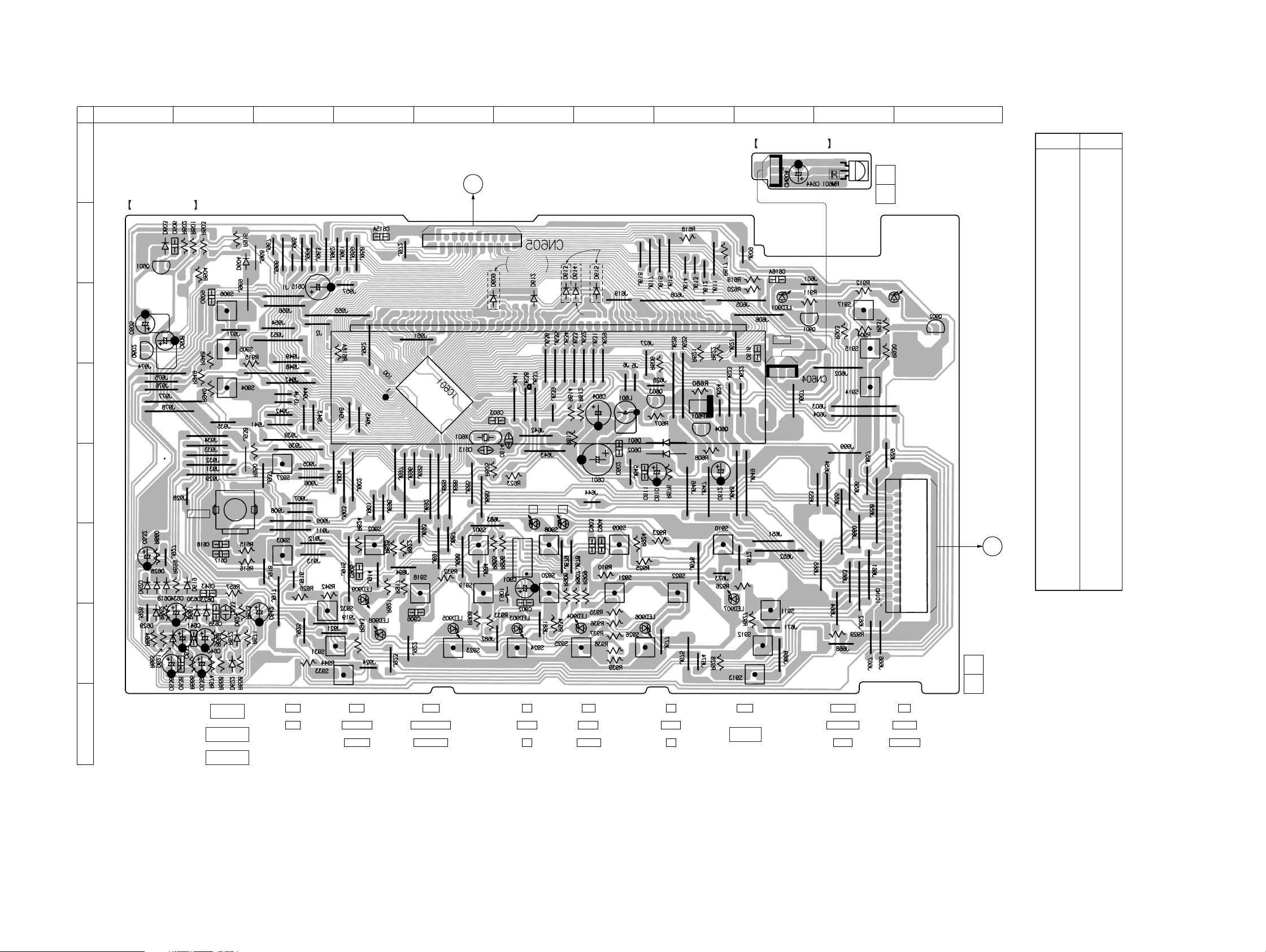
1. Addition of Printed Wiring Board
PRINTED WIRING BOARD – PANEL Section –
HCD-BX2/DX2/DX2B
1 2 3 4 5 6 7 8 9 10 11
SENSOR BOARD
A
DECORD BOARD
A
CN705
1
3
FRONT BOARD
1
3
1-678-507-
11
(11)
• Semiconductor
Location
Ref. No. Location
D601 D-8
D602 E-8
D603 B-1
D604 B-2
D609 C-6
D612 C-6
D613 C-6
D614 C-7
22
B
ECB
21
2
1
AEP, UK, E2, E3,
SP, TW, AR
(US, CND, MX)
D615 C-7
D618 F-1
D619 F-2
D620 F-1
D621 G-1
LED902
(STANDBY)
(AEP, UK)
C
FLD601
ECB
81 80
D
FLOURESCENT INDICATOR
30 31
TUBE
51
50
ECB
21
ECB
491
LED901
TIMER
213
ECB
BCE
D622 G-2
D623 G-2
D624 G-2
D628 F-1
D629 G-1
D630 G-2
IC601 D-5
IC602 F-6
LED901 C-9
LED902 C-11
LED903 G-6
LED904 G-7
LED905 G-5
LED906 G-7
LED907 F-8
LED908 G-4
LED909 F-4
E
LED911
VR602
VOLUME
LED910
G
g
30
29
LED910 E-6
LED911 E-6
Q601 B-1
Q602 C-1
IC602
89
F
116
C
MAIN
BOARD
CN601
Q603 D-8
Q604 D-8
Q901 C-9
Q902 C-11
RM601 A-10
2
1
G
11
1-678-576-
S906
PLAY MODE
DIRECTION
H
05
S905
REPEAT
STEREO/MONO
S904
TUNER MEMORY
EDIT
S927
j
S903
J
LED909, S932
REC
LED908, S931
REC PAUSE
S933
CD SYNC
S902
> +
S918
Z OPEN/CLOSE
LED905, S923
TUNER/BAND
S907
X
S919
DISC 3
LED903, S924
CD
S908
g G
S920
DISC 2
LED904, S925
TAPE A/B
S909
x
S921
DISC 1
LED906, S926
MD
S910
– .
S922
DISC SKIP
EX-CHANGE
LED907, S911
GROOVE
S912
FILE SELECT
S913
ENTER
S917
I/1
S915
DISPLAY
S914
SPECTRUM
(11)
Note on Printed Wiring Board:
• Y : parts extracted from the conductor side.
• C : panel designation.
• b : Pattern from the side which enables seeing.
(The other layers' patterns are not indicated.)
• Abbreviation
AR : Argentine model
AUS : Australian model
CND : Canadian model
E2 : 120 V AC Area in E model
E3 : 240 V AC Area in E model
KR : Korean model
MX : Mexican model
SP : Singapore model
TW : Taiwan model
33
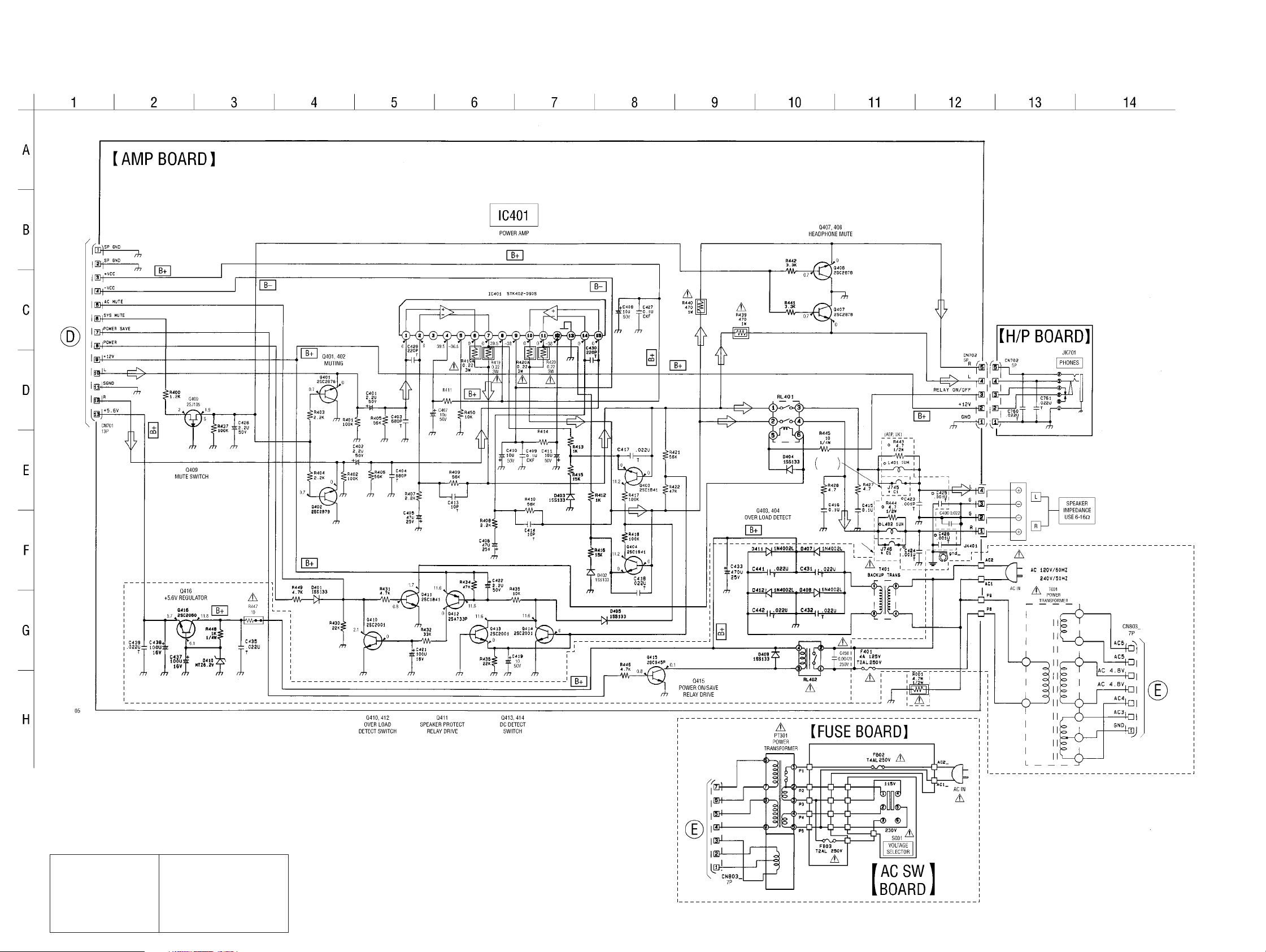
HCD-BX2/DX2/DX2B
2. Addition of Information of Destination
• SCHEMATIC DIAGRAM – AMP/POWER SUPPLY Section –
(BX2/DX2 : SP, TW, KR, MX, AUS models)
(BX2/DX2: MX)
*
*R411, 414
100 (AEP, UK)
12k (EXCEPT AEP, UK)
*
EXCEPT
AEP, UK
100V
(BX2/DX2: MX)
100V
(EXCEPT AEP, UK)
(US, CND, MX)
(AEP, UK, KR, AUS)
(BX2/DX2 : KR, MX, AUS)
(US, CND, MX)
Note on Schematic Diagram:
• All capacitors are in µF unless otherwise noted. U: µF,
pF: µµF 50 WV or less are not indicated except for
electrolytics and tantalums.
• If a numeric value of capacitor is a decimal fraction, the
preceding zero may be omitted.
(For example, .1 expresses 0.1)
• All resistors are in Ω and 1/
specified.
4
W or less unless otherwise
• 5 : fusible resistor.
• 2 : nonflammable resistor.
• C : panel designation.
Note:
The components identified by mark 0 or dotted
line with mark 0 are critical for safety.
Replace only with part
number specified.
Note:
Les composants identifiés par
une marque 0 sont critiques
pour la sécurité.
Ne les remplacer que par une
pièce portant le numéro
spécifié.
• U : B+ Line.
• V : B– Line.
• Voltages are dc with respect to ground under no-signal
(detuned) conditions.
no mark : FM
• Voltages are taken with a V OM (Input impedance 10 MΩ).
Voltage var iations may be noted due to normal production tolerances.
• Signal path.
F : FM
• Abbreviation
AUS : Australian model
CND : Canadian model
KR : Korean model
MX : Mexican model
SP : Singapore model
TW : Taiwan model
(SP, TW)
44
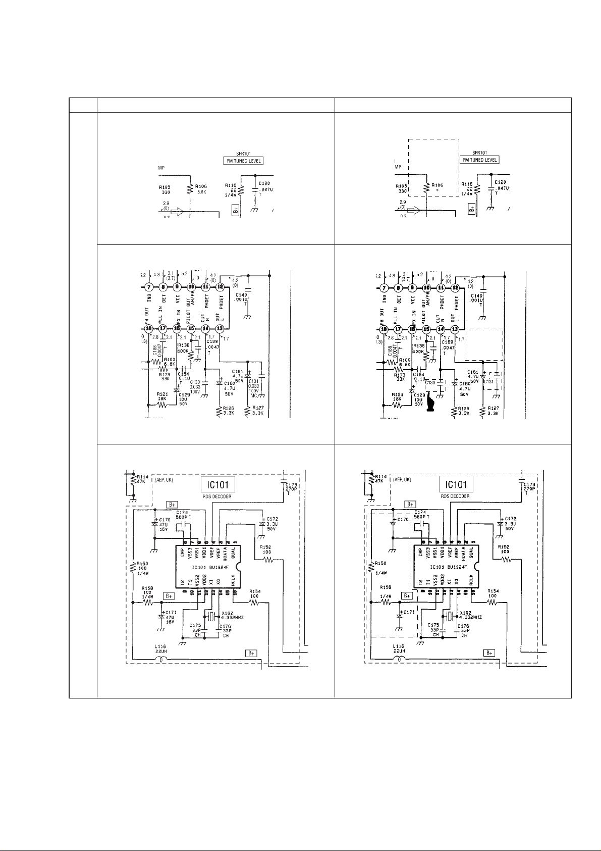
HCD-BX2/DX2/DX2B
• SCHEMATIC DIAGRAM
! : Indicates changed portion.
Page Before Change After Change
Location A – B, 9 – 11
Location D – F, 14 – 17
20
R106
*
5.6k (US, CND, E, AUS)
100 (AEP,UK)
*
^
C130, C131
*
0.033 100V
(US, CND, E, AUS)
0.0022 100V
(AEP, UK)
^
*
@
Location G – J, 4 – 7
12k
#
22
25V
12k
22
25V
– Continued on next page –
5
 Loading...