

Page 1
HCD-DR7AV/XB800AV
SERVICE MANUAL
HCD-DR7AV/XB800AV is the tuner,
deck, CD and amplifier section in
LBT-DR7AV/XB800AV.
SECTION
TAPE DECK
SECTION
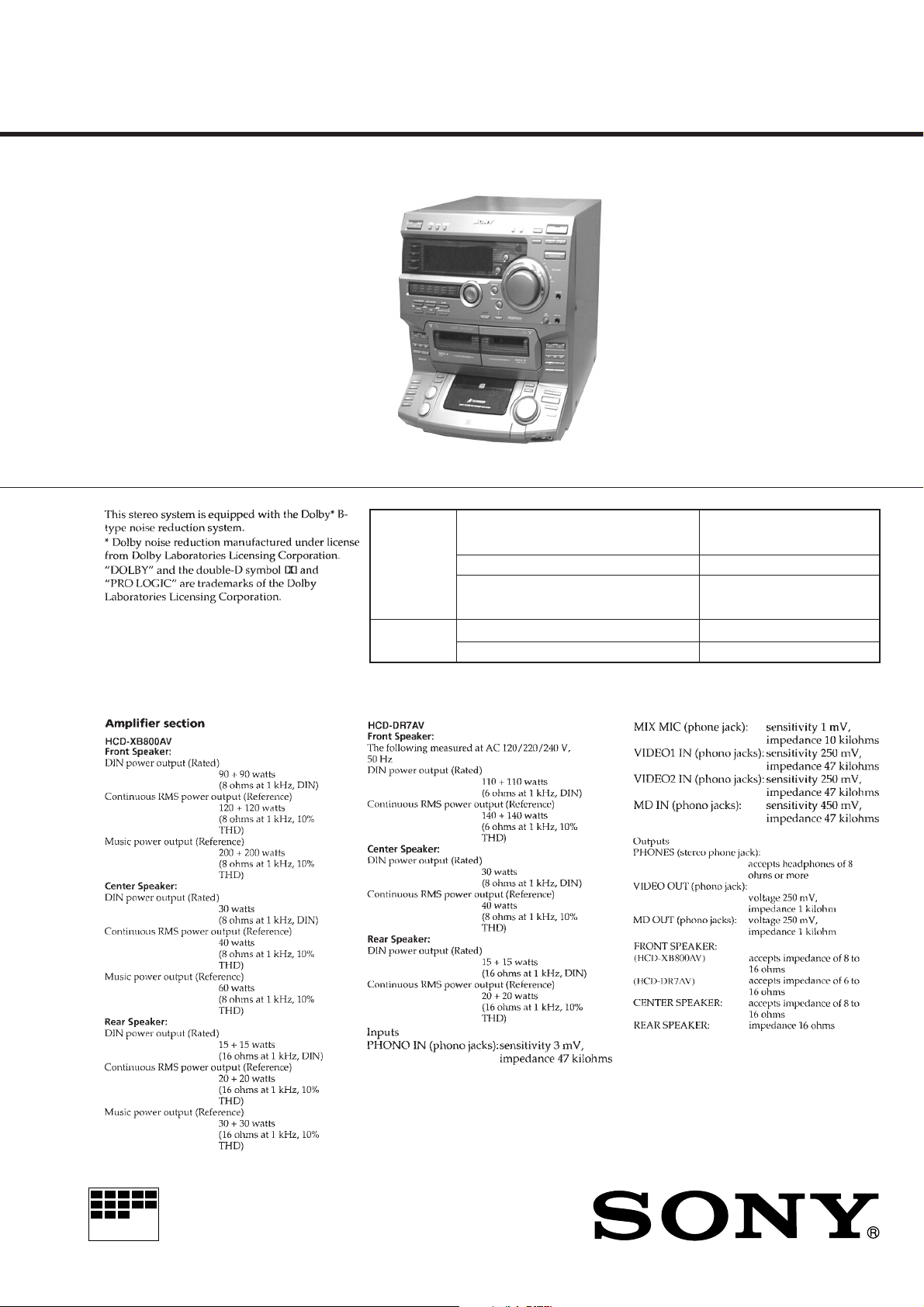
Photo: HCD-DR7AV
Model Name Using Similar Mechanism HCD-DR4/DR5/DR6/DR440/
CD
CD Mechanism Type CDM37M-5BD32L
Base Unit Type BU-5BD32L
Optical Pick-up Type KSS-213D/Q-N
Model Name Using Similar Mechanism NEW
T ape Transport Mechanism T ype TCM-230AWR2/230PWR2
AEP Model
UK Model
HCD-XB800AV
E Model
Australian Model
HCD-DR7AV
W300/W5000/XB500
SPECIFICATIONS
COMPACT DISC DECK RECEIVER
— Continued on next page —
MICROFILM
– 1 –
Page 2
– 2 –
Page 3
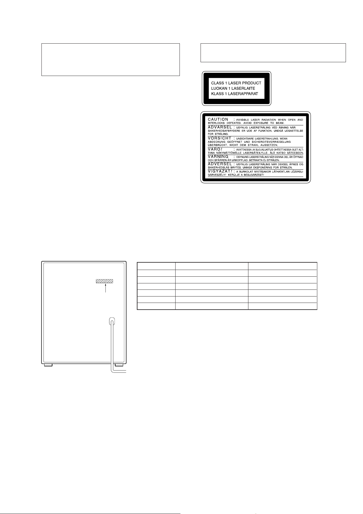
CAUTION
Use of controls or adjustments or performance of procedures
other than those specified herein may result in hazardous radiation exposure.
Notes on chip component replacement
• Never reuse a disconnected chip component.
• Notice that the minus side of a tantalum capacitor may be
damaged by heat.
Laser component in this product is capable of emitting radiation
exceeding the limit for Class 1.
This appliance is classified as
a CLASS 1 LASER product.
The CLASS 1 LASER PRODUCT MARKING is located on
the rear exterior.
Flexible Circuit Board Repairing
• Keep the temperature of soldering iron around 270˚C
during repairing.
• Do not touch the soldering iron on the same conductor of the
circuit board (within 3 times).
• Be careful not to apply force on the conductor when soldering
or unsoldering.
MODEL IDENTIFICATION
— BACK PANEL —
PARTS No. MODEL PRODUCT COUNTRY
4-214-788-0π DR7AV: SP INDONESIA
4-214-788-1π DR7AV: EA INDONESIA
4-214-788-2π DR7A V: AUS INDONESIA
Parts No.
4-214-788-6π DR7AV: TH THAILAND
4-214-785-3π XB800AV: AEP, UK, EE, CIS INDONESIA
4-214-785-4π XB800A V: AEP THAILAND
This caution
label is located
inside the unit.
• Abbreviation
SP : Singapore model
EA : Saudi Arabia model
AUS : Australian model
TH : Thailand model
EE : East European model
SAFETY-RELATED COMPONENT WARNING !!
COMPONENTS IDENTIFIED BY MARK ! OR DO TTED LINE
WITH MARK ! ON THE SCHEMATIC DIAGRAMS AND IN
THE PARTS LIST ARE CRITICAL TO SAFE OPERATION.
REPLACE THESE COMPONENTS WITH SONY PARTS
WHOSE PART NUMBERS APPEAR AS SHOWN IN THIS
MANUAL OR IN SUPPLEMENTS PUBLISHED BY SONY.
– 3 –
Page 4

NOTES ON HANDLING THE OPTICAL PICK-UP BLOCK
OR BASE UNIT
SECTION 1
SERVICING NOTE
The laser diode in the optical pick-up block may suffer electrostatic
break-down because of the potential difference generated by the
charged electrostatic load, etc. on clothing and the human body.
During repair, pay attention to electrostatic break-down and also
use the procedure in the printed matter which is included in the
repair parts.
The flexible board is easily damaged and should be handled with
care.
NOTES ON LASER DIODE EMISSION CHECK
The laser beam on this model is concentrated so as to be focused on
the disc reflective surface by the objective lens in the optical pickup block. Therefore, when checking the laser diode emission, observe from more than 30 cm away from the objective lens.
LASER DIODE AND FOCUS SEARCH OPERATION
CHECK
Carry out the “S curve check” in “CD section adjustment” and check
that the S curve waveform is output four times.
About CD-TEXT display
This unit is provided with a simple CD-TEXT display function.
The CD-TEXT contents of 20 tracks are displayed on the fluorescent display tube.
Since the function is simple, some special characters may not be
displayed, or may be displayed as other characters.
– 4 –
Page 5

TABLE OF CONTENTS
1. SERVICING NOTE .......................................................... 4
2. GENERAL ....................................................................6
3. DISASSEMBLY
3-1. Front Panel ............................................................................ 8
3-2. Main Board ........................................................................... 8
3-3. Sub Panel .............................................................................. 9
3-4. CD-L/CD-R Board and CD Lid Assembly ........................... 9
3-5. Tape Mechanism Deck and Cassette Lid ............................ 10
3-6. CD Mechanism Deck .......................................................... 10
3-7. Base Unit ............................................................................. 10
3-8. Disc Table ........................................................................... 11
4. SERVICE MODE ............................................................ 12
5. MECHANICAL ADJUSTMENTS ..........................16
6. ELECTRICAL ADJUSTMENTS ............................... 16
7. DIAGRAMS
7-1. Circuit Boards Location ...................................................... 19
7-2. Block Diagrams
• BD (CD) Section.............................................................. 21
• Deck Section .................................................................... 23
• Main (1/2) Section ........................................................... 25
• Main (2/2) Section ........................................................... 27
• Power Section (DR7AV model)....................................... 29
• Power Section (XB800AV model)................................... 31
• Display Section ................................................................ 33
7-3. Printed Wiring Board – BD (CD) Section – ....................... 37
7-4. Schematic Diagram – BD (CD) Section – .......................... 39
7-5. Printed Wiring Board – Main Section – .............................. 41
7-6. Schematic Diagram – Main (1/5) Section – ........................ 43
7-7. Schematic Diagram – Main (2/5) Section – ........................ 45
7-8. Schematic Diagram – Main (3/5) Section – ........................ 47
7-9. Schematic Diagram – Main (4/5) Section – ........................ 49
7-10. Schematic Diagram – Main (5/5) Section – ..................... 51
7-11. Schematic Diagram – Deck Section – .............................. 53
7-12. Printed Wiring Board – Deck Section – ........................... 55
7-13. Schematic Diagram – Power (1/2) Section –
(DR7AV model)................................................................ 57
7-14. Schematic Diagram – Power (2/2) Section –
(DR7AV model)................................................................ 59
7-15. Printed Wiring Board – Power Section –
(DR7AV model)................................................................ 61
7-16. Schematic Diagram – Power (1/2) Section –
(XB800AV model)............................................................ 63
7-17. Schematic Diagram – Power (2/2) Section –
(XB800AV model)............................................................ 65
7-18. Printed Wiring Board – Power Section –
(XB800AV model)............................................................ 67
7-19. Schematic Diagram – Panel FL Section – ........................69
7-20. Printed Wiring Board – Panel FL Section – ..................... 71
7-21. Schematic Diagram – Panel VR Section – .......................73
7-22. Printed Wiring Board – Panel VR Section – .................... 75
7-23. Schematic Diagram – TC Panel Section – ....................... 77
7-24. Printed Wiring Board – TC Panel Section –..................... 79
7-25. Schematic Diagram – CD Panel Section – ....................... 81
7-26. Printed Wiring Board – CD Panel Section – .................... 83
7-27. Schematic Diagram – CD Motor Section – ...................... 85
7-28. Printed Wiring Board – CD Motor Section –................... 87
7-29. Schematic Diagram – Jack Section – ............................... 89
7-30. Printed Wiring Board – Jack Section – ............................ 91
7-31. Schematic Diagram – Trans Section –
(XB800AV model)............................................................ 93
7-32. Printed Wiring Board – Trans Section –
(XB800AV model)............................................................ 95
7-33. Schematic Diagram – Trans Section –
(DR7AV model)................................................................ 97
7-34. Printed Wiring Board – Trans Section –
(DR7AV model)................................................................ 99
7-35. Schematic Diagram – Leaf SW Section – ...................... 100
7-36. Printed Wiring Board – Leaf SW Section – ................... 100
7-37. Schematic Diagram – Surround Section – ..................... 101
7-38. Printed Wiring Board – Surround Section –................... 101
7-39. IC Block Diagrams ......................................................... 103
7-40. IC Pin Functions ............................................................. 104
8. EXPLODED VIEWS
8-1. Case and Back Panel Section ............................................ 107
8-2. Front Panel Section 1 ........................................................ 108
8-3. Front Panel Section 2 ........................................................ 109
8-4. Chassis Section ................................................................. 110
8-5. TC Mechanism Section 1 (TCM230AWR2/230PWR2)... 111
8-6. TC Mechanism Section 2 (TCM230AWR2/230PWR2)... 112
8-7. CD Mechanism Section (CDM37M-5BD32L) ................. 113
8-8. Base Unit Section (BU-5BD32L) ..................................... 114
9. ELECTRICAL PARTS LIST ...................................... 115
– 5 –
Page 6
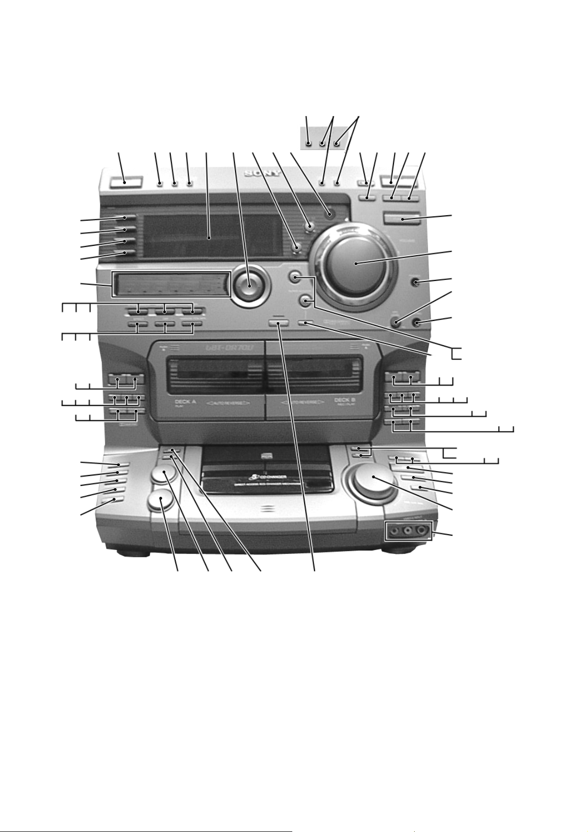
Front Panel
SECTION 2
GENERAL
10 11 12
66
63
71
70
69
68
67
65
55
64
6162
5960
565758
54
1
2
34
56
79
8
14 15 16 17
13
25
26
28
27
29
18
19
20
21
22
30
23
24
31 32
33
34
53
52
51
50
49
48
47
35
37
36
39
40
41
42
43
444546
38
– 6 –
Page 7
LOCATION OF PARTS AND CONTROLS
1 1/u (Power) button and indicator
2 DEMO (STANDBY) button (DR7AV)
POWER SAVE/DEMO (STANDBY)
button (XB800AV)
3 DISPLAY button
4 SPECTRUM ANALYZER button
5 Display window
6 GEQ control button
7 SYNC BASS button
8 SYNC EQ button
9 Remote sensor
10 PTY button (XB800AV)
11 TUNING MODE button
12 STEREO/MONO button
13 ENTER/NEXT button and indicator
14 TUNER MEMORY button
15 TUNER/BAND button
16 TUNING - button
17 TUNING + button
18 FUNCTION button
19 VOLUME knob
20 PHONES jack
21 MIC LEVEL knob
22 MIX MIC jack
23 GROOVE button and indicator
24 SUPER WOOFER button and indicator
25 MODE button
26 ª (B Deck) button and indicator
27 · (B Deck) button and indicator
28 p (B Deck) button
29 0 (B Deck) button
30 ) (B Deck) button
31 P (B Deck) button
32 r REC (B Deck) button
33 HI-SPEED DUB button
34 CD SYNCHRO button
35 PLAY MODE button
36 REPEAT button
37 0 (CD) button
38 ) (CD) button
39 ·P (CD) button and indicator
40 p (CD) button
41 DISK SKIP button
42 = AMS + knob
43 VIDEO2 INPUT jacks
44 PRO LOGIC button and indicator
45 EDIT button
46 NON-STOP button and indicator
47 LOOP button
48 FLASH button
49 DISC 5 button
50 DISC 4 button
51 DISC 3 button
52 DISC 2 button
53 DISC 1 button
54 DOLBY NR button
55 DIRECTION button
56 ) (A Deck) button
57 0 (A Deck) button
58 p (A Deck) button
59 · (A Deck) button
60 ª (A Deck) button
61 KARAOKE PON/MPX button
62 DSP button and indicator
63 EFFECT button and indicator
64 ENTER button and indicator
65 GEQ CONTROL button
66 P. FILE MEMORY
67 Equalizer indicators
68 t/CLOCK SET button
69 SLEEP button
70 REC button and indicator
71 DAILY button and indicator
• AMS is the abbreviation for Automatic
Music Sensor.
This section is extracted from
instruction manual.
– 7 –
Page 8
SECTION 3
)
)
)
DISASSEMBLY
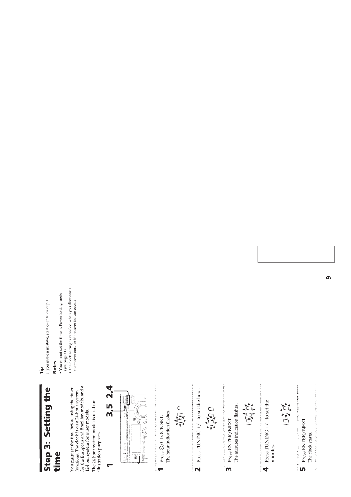
Note: Follow the disassembly procedure in the numerical order given.
3-1. FRONT PANEL
3
Connector (CN452)
2
Connector (CN702)
1
Three flat type wires
(CN303,CN304,CN431)
4
7
Front panel
Connector (CN802)
3-2. MAIN BOARD
!¢
Back panel
!£
Power cord
!™
Screw (BVTP 3x8)
(HCD-XB800AV)
6
Four screw (BVTP 3x8)
2
Two screws (BVTP 3x8)
9
8
7
5
Screw (BVTP 3x8
Four screws (BVTP 3x8)
0
Two screws (BVTP 3x8)
(HCD-DR7AV)
Five screws (BVTP 3x8)
Seven screws (BVTP 3x8)
!§
Main board
6
Connector (CN903)
(HCD-DR7AV)
1
Flat type wire (CN1
!¡
Fan motor
(HCD-DR7AV)
5
Flat type wire (CN411)
4
Connector (CN412)
– 8 –
3
T uner unit
!∞
Two screws (BVTP 3x8
Page 9
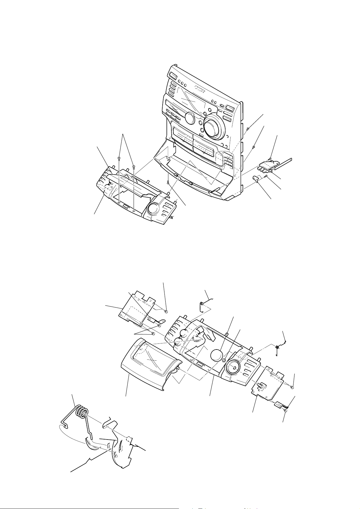
3-3. SUB PANEL
4
Two screws (BTP 2.6x6)
3
Open the CD lid assembly
8
Sub panel block
5
Screw (BVTP 3x8)
7
Three screws (BVTP 2.6x8)
6
Two screws (BVTP 2.6x8)
1
Two screws (BVTP 2.6x8)
2
Front input board
9
Two screws (BVTP 2.6x8)
0
Bracket (CD-R2)
3-4. CD-L/CD-R BOARD AND CD LID ASSEMBLY
1
Three screws (BVTP 2.6x8)
3
Bracket (CD-L)
4
CD-L board
2
Three screws
(BVTP 2.6x8)
Torsion spring (CD-L)
!£
CD lid assembly
!™
Torsion spring (CD-L)
Sub panel assembly
5
Knob (CD)
6
Nut
0
CD-R board
!¡
Torsion spring (CD-R)
7
Three screws
(BVTP 2.6x8)
9
Bracket (CD-R)
8
Two screws (BVTP 2.6x8)
Sub panel assembly
CD lid assembly
– 9 –
Page 10
3-5. TAPE MECHANISM DECK AND CASSETTE LID
t
Claw
Holder assembly
Claw
Claw
6
Holder (A) assembly
(Refer to lower figure)
1
8
Torsion spring (TC-A)
Three screws (BVTP 2.6x8)
2
Three screws
(BVTP 2.6x8)
Cassette lid assembly
4
Cassette lid (A) assembly
(Refer to upper figure)
Claw
5
Cassette lid (B) assembly
(Refer to upper figure)
Portion
A
Portion
B
Portion
3-6. CD MECHANISM DECK 3-7. BASE UNIT
1
Five screws (BVTP3x8)
9
Torsion spring (TC-B)
7
Holder (B) assembly
(Refer to lower figure)
Portion
A
B
3
T ape mechanism
2
CD mechanism
deck
3
Base uni
2
Boss
1
Yoke fitting
– 10 –
Page 11
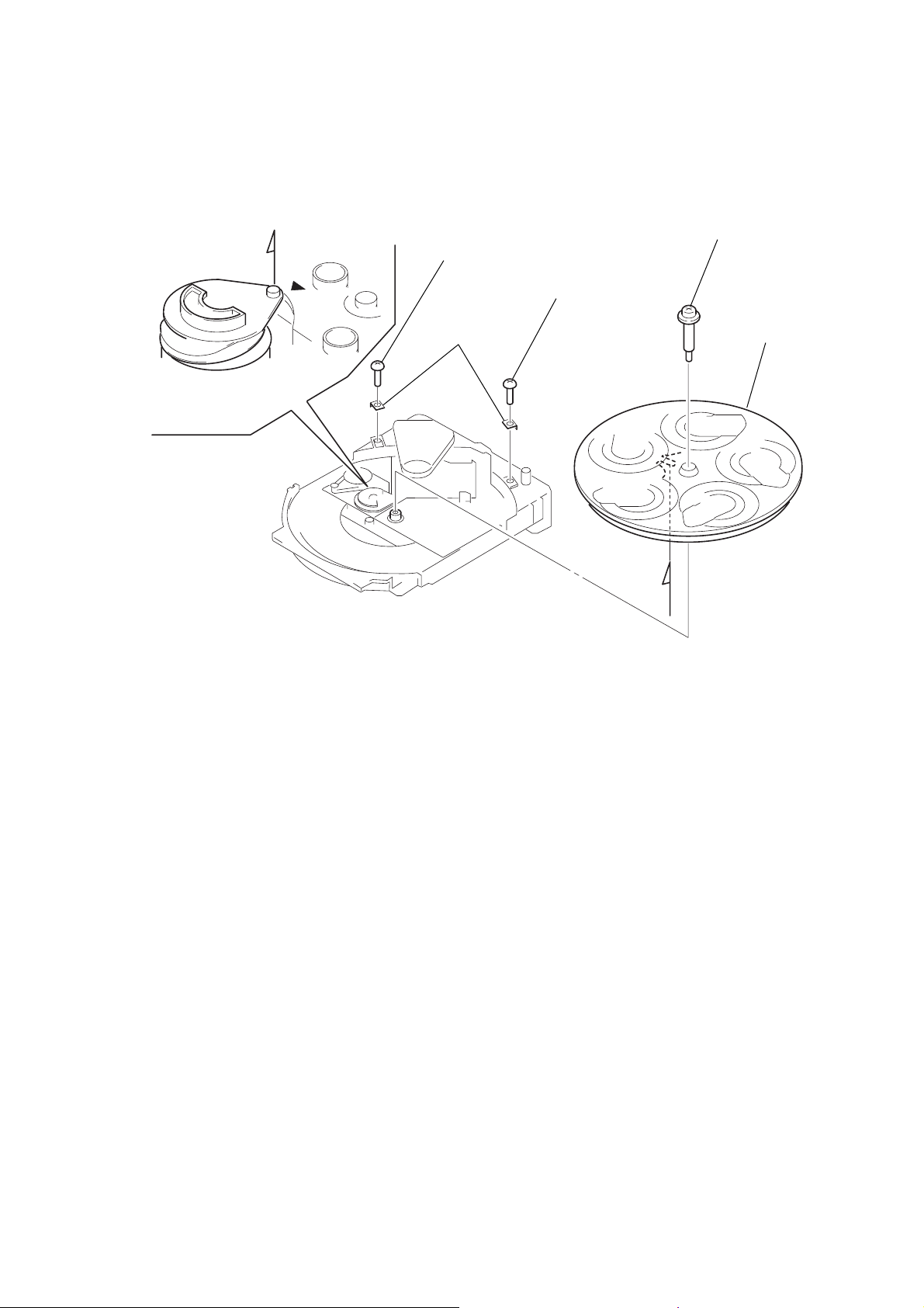
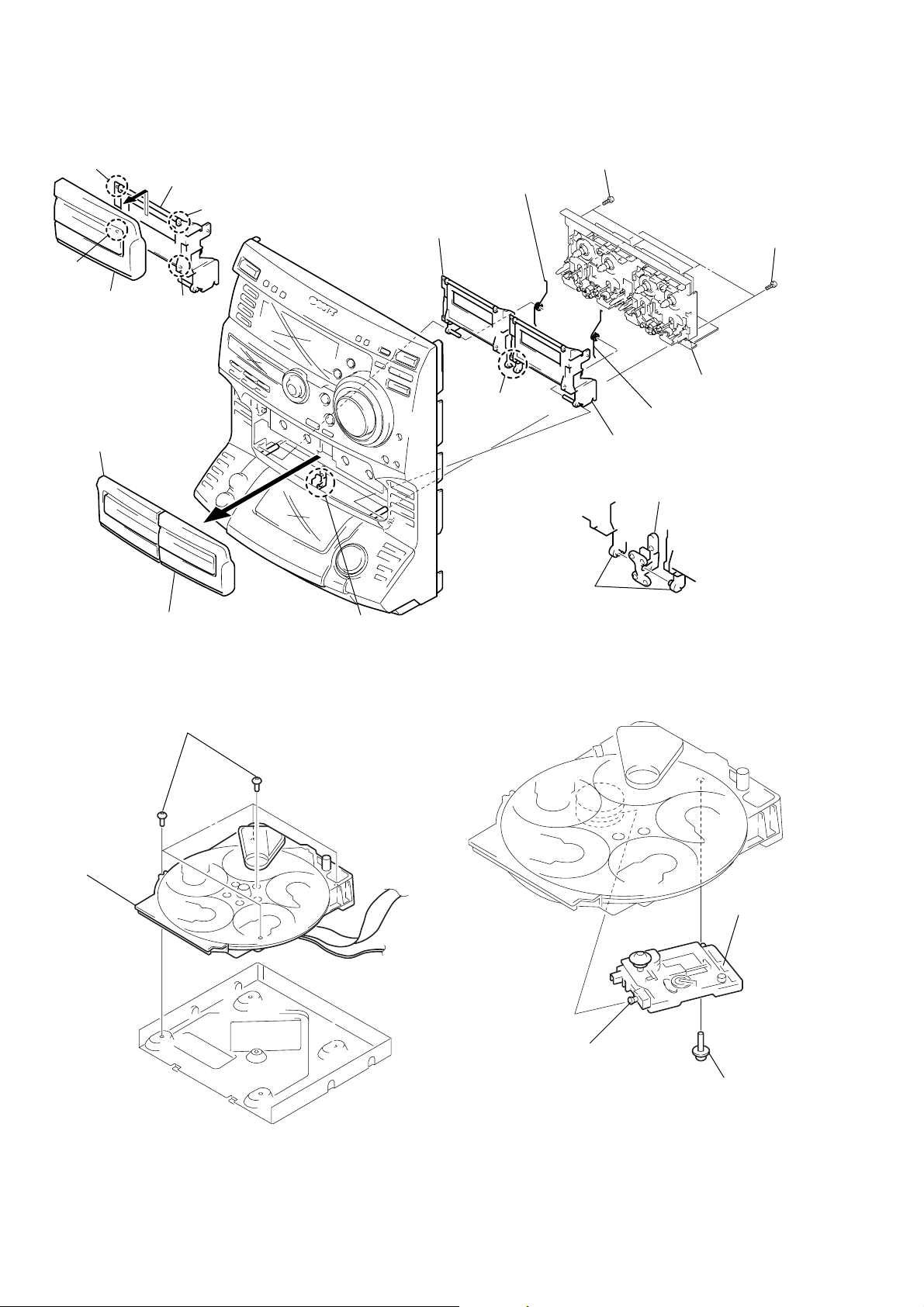
3-8. DISC TABLE
Note:
When the disc table is installed, adjust the positions of
roller cam and mark ” as shown in the figure, then set to
the groove of disc table.
A
2
Screw (BVTP3X8)
3
Bracket (BU)
1
Screw (BVTP3X8)
4
Stop screw
5
Disc table
A
– 11 –
Page 12

SECTION 4
SERVICE MODE
MC Cold Reset
• The cold reset clears all data including preset data stored in the RAM to initial conditions. Execute this mode when returning the set to the
customer.
Procedure:
1. Press three buttons t/CLOCK SET , ENTER , and 1/u simultaneously.
2. “COLD RESET” is displayed on the fluorescent display tube and reset is executed.
CD Delivery Mode
• This mode moves the pick-up to the position durable to vibration. Use this mode when returning the set to the customer after repair.
Procedure:
1. Press 1/u button to turn the set ON.
2. Press LOOP button and 1/u button simultaneously.
3. A message “LOCK” is displayed on the fluorescent indicator tube, and the CD delivery mode is set.
MC Hot Reset
• This mode resets the set with the preset data kept stored in the memory . The hot reset mode functions same as if the po wer cord is plugged
in and out.
Procedure:
1. Press three buttons t/CLOCK SET , ENTER , and DISC 1 simultaneously.
2. The fluorescent indicator tube becomes blank instantaneously, and the set is reset.
Sled Servo Mode
• This mode can run the CD sled motor freely. Use this mode, for instance, when cleaning the pick-up.
Procedure:
1. Press 1/u button to turn the set ON.
2. Press three buttons t/CLOCK SET , ENTER , and DISC 5 simultaneously.
3. The Sled Servo mode is selected, if “CD” is blanking on the fluorescent indicator tube.
4. With the CD in stop status, When the = AMS + knob is rotated in the clockwise direction, the pick-up moves outside. When
rotated counterclockwise, it moves inside.
5. To exit from this mode, perform as follows:
1) Move the pick-up to the most inside track.
2) Execute MC cold reset. (Press the three buttons t/CLOCK SET , ENTER , and 1/u button simultaneously.)
Note:
• Always move the pick-up to most inside track when exiting from this mode. Otherwise, a disc will not be unloaded.
• Do not run the sled motor excessively, otherwise the gear can be chipped.
Change-over of AM Tuner Step between 9kHz and 10kHz (DR7AV Only)
• A step of AM channels can be changed over between 9kHz and 10kHz.
Procedure:
1. Press 1/u button to turn the set ON.
2. Select the function “TUNER”, and press TUNER/BAND button to select the BAND “AM”.
3. Press 1/u button to turn the set OFF.
4. Press ENTER and 1/u buttons simultaneously, and the display of fluorescent indicator tube changes to “AM 9k STEP” or “AM 10k
STEP”, and thus the channel step is changed over.
LED and Fluorescent Indicator Tube All Lit, Key Check Mode
Procedure:
1. Press three buttons t/CLOCK SET , ENTER , and DISC 2 simultaneously.
2. LEDs and fluorescent indicator tube are all turned on.
Press DISC 2 button, and the key check mode is activated.
3. In the key check mode, the fluorescent indicator tube displays “K @ V0 J0”. Each time a button is pressed , “K”value increases. Howe ver ,
once a button is pressed, it is no longer taken into account.
“J” Value increases like 1, 2, 3 ... if rotating = AMS + knob in “+” direction, or it decreases like 0, 9, 8 ... if rotating in “-”
direction.
“V” Value increases like 1, 2, 3 ... if rotating VOLUME knob in “+” direction, or it decreases like 0, 9, 8 ... if rotating in “-” direction.
4. To exit from this mode, press three buttons in the same manner as step 1, or disconnect the power cord.
– 12 –
Page 13

AMS Test Mode
• This mode is used for checking the AMS operations of the tape deck.
JIG
7-819-039-12 Alignment tape, AMS-110A
Procedure:
1. Press the 1/u button to turn the set ON.
2. Set the tape (AMS-110A).
3. Press the three buttons t/CLOCK SET , ENTER , and DISC 3 button simultaneously.
4. “TEST MODE” is displayed on the fluorescent display tube.
5. Press the FUNCTION button and switch the function to the deck with the tape (AMS-110A).
6. Press the CD SYNCHRO button. “AMS CHECK” is displayed on the fluorescent display tube and the tape is rewound.
7. AMS starts in the normal direction. If the AMS count is 2 at shut down, proceed to step 8.
“NG” is displayed at other times, and the deck stops.
8. AMS starts in the opposite direction. If the AMS count is 2 at shut down again, “OK” is displayed.
“NG” is displayed at other times.
Aging Mode
During the aging mode, both the CD player and tape deck are executed together.
• If an error occurs:
Aging stops, and the error state is displayed on the fluorescent display tube.
• If no error occurs:
Aging is repeated.
Procedure:
1. Press the 1/u button to turn the set ON.
2. Load 10 minute tapes with unbent rec-proof tabs in decks A and B.
3. Set CDs on the DISC 1 and DISC 4 tables.
4. Set the CD mode REPEAT to OFF and PLAY MODE to ALL DISCS.
(Press the PLAY MODE and REPEAT buttons to set these modes.)
5. Press the FUNCTION button to switch the function to “CD”.
6. Press the three buttons t/CLOCK SET , ENTER , and DISC 4 button simultaneously.
7. Aging starts.
8. To end aging, press the 1/u button to turn the set OFF.
Aging Sequence:
Aging is performed in the following sequence.
• T ape Deck
1. The tape in deck A is rewound. “TAPE A AG-1” is displayed.
2. The FWD side of deck A is played for two minutes.
“TAPE A AG-2” is displayed.
3. The tape in deck A is fast forwarded. “TAPE A AG-3” is displayed. Fast forward is carried out for 20 seconds or to the tape end.
4. The RVS side of deck A is played for two minutes.
“TAPE A AG-4” is displayed.
5. The tape in deck A is rewound. “TAPE A AG-5” is displayed.
6. The FWD side of deck B is played for two minutes.
“TAPE B AG-2” is displayed.
7. The tape in deck B is fast forwarded. “TAPE B AG-3” is displayed. Fast forward is carried out for 20 seconds or to the tape end.
8. The RVS side of deck B is played for two minutes.
“TAPE B AG-4” is displayed.
9. The tape in deck A is rewound. “TAPE A AG-5” is displayed.
10. Repeated from step 2.
• CD
1. The tray rotates.
2. DISC 1 is chucked.
3. The TOC is read.
4. The first track is played for 2 seconds.
5. The last track is played for 2 seconds.
6. The tray rotates.
7. DISC 4 is chucked.
8. The TOC is read.
9. The first track is played for 2 seconds.
10. The last track is played for 2 seconds.
11. Repeated from step 1.
– 13 –
Page 14

• Display when ended abnormally
When the tape deck is abnormal:
The state when ended abnormally is displayed.
The contents of display are the same as that during aging.
When the CD player is abnormal:
A message indicating that errors such as “CD MEC ERR” have occurred.
Check the error contents in the following error history display mode.
Error History Display Mode
Mode which enables the history of error occurring in the CD player to be checked.
Execute this mode after ending the aging mode.
Procedure:
1. Press the 1/u button to turn the set ON.
2. Press the three buttons t/CLOCK SET , ENTER , and CD SYNCHRO simultaneously.
3. A message such as “EMC@@EDC**” is displayed.
@@ : Number of mechanical errors (Up to three past errors)
** : Number of errors (NO DISC ERROR) which occurs after chucking (Up to three past errors)
4. When checking the history of mec hanical errors, press the PLAY MODE button. When checking errors after chucking, press the
REPEAT button to switch the display.
5. Press the 1/u button to end and turn the set OFF.
6. To erase the error history, perform COLD reset.
(Press the three buttons t/CLOCK SET , ENTER , and DISC 1 simultaneously.
• Viewing the mechanical error history display
(Switch the history by pressing the PLAY MODE button.)
Display
E@@M#*****
@@ : Error number. 00 is the newest.
# : Operating state of table
0 : Currently in the INITIAL mode
7 : Currently rotating to the right
8 : Currently rotating to the left
A : Currently chucking down
B : Currently chucking up
* : Inv alid
• Viewing the NO DISC ERROR history display
(Switch the history by pressing the REPEAT button.)
Display
E@@D##$$%*
@@ : Error number. 00 is the newest
## : Error contents
01: Focus error
02: GFS error
03: Setup error
$$ : Retries
00: NO DISC is determined without attempting chucking
retry
02: NO DISC is determined after chucking retry.
% : State when determined as NO DISC
1 : When stopped
2 : At setup
3 : At TOC READ
4 : When accessing
5 : When playing
6 : When pausing
7 : When manual searching (during play)
8 : When manual searching (during pausing)
* : Inv alid
– 14 –
Page 15
SECTION 5
MECHANICAL ADJUSTMENTS
SECTION 6
ELECTRICAL ADJUSTMENTS
Precaution
1. Clean the following parts with a denatured alcohol-moistened
swab:
record/playback heads pinch rollers
erase head rubber belts
capstan idlers
2. Demagnetize the record/playback head with a head demagnetizer.
3. Do not use a magnetized screwdriver for the adjustments.
4. After the adjustments, apply suitable locking compound to the
parts adjusted.
5. The adjustments should be performed with the rated power supply voltage unless otherwise noted.
Torque Measurement
Mode
FWD
FWD
back tension
REV
REV
back tension
FF/REW
FWD tension
REV tension
Torque meter
CQ-102C
CQ-102C
CQ-102RC
CQ-102RC
CQ-201B
CQ-403A
CQ-403R
Meter reading
31 to 71 g • cm
(0.43 – 0.98 oz • inch)
2 to 6 g • cm
(0.02 – 0.08 oz • inch)
31 to 71 g • cm
(0.43 – 0.98 oz • inch)
2 to 6 g • cm
(0.02 – 0.08 oz • inch)
71 to 143 g • cm
(0.98 – 1.99 oz • inch)
100 g or more
(3.53 oz or more)
100 g or more
(3.53 oz or more)
DECK SECTION 0 dB=0.775V
1. Demagnetize the record/playback head with a head damagnetizer .
2. Do not use a magnetized screwdriver for the adjustments.
3. After the adjustments, apply suitable locking compound to the
parts adjusted.
4. The adjustments should be performed with the rated power supply voltage unless otherwise noted.
5. The adjustments should be performed in the order given in this
service manual. (As a general rule, playback circuit adjustment
should be completed before performing recording circuit adjustment.)
6. The adjustments should be performed for both L-CH and R-CH.
7. Switches and controls should be set as follows unless otherwise
specified.
Signal
P-4-A100
WS-48B
P-4-L300
10 kHz, –10 dB
3 kHz, 0 dB
315 Hz, 0 dB
Record/Playback Head Azimuth Adjustment
(Deck A, Deck B)
Note: Perform this adjustments for both decks.
Procedure:
1. Mode : Playback
Used forTape
Azimuth Adjustment
Tape Speed Adjustment
Level Adjustment
test tape
P-4-A100
(10kHz, –10dB)
set
MD OUT
level meter
+
–
2. Turn the adjustment screw and check output peaks. If the peaks
do not match for L-CH and R-CH, turn the adjustment screw so
that outputs match within 1 dB of peak.
L-CH
peak
screw
position
R-CH
peak
output
level
within
1 dB
L-CH
peak
R-CH
peak
within 1dB
screw
position
– 15 –
Page 16
3. Mode: Playback Tape Speed Adjustment (Deck A)
)
test tape
P-4-A100
(10kHz, –10dB)
oscilloscope
MD OUT
Note: Set the test mode using the following method and begin tape
speed adjustment.
In the test mode, the speed will switch to double speed or
normal speed each time the HI-SPEED DUB button is pressed.
set
Waveform of oscilloscope
in phase 45
good
°
90
135
°
°
wrong
180
°
4. After the adjustments, apply suitable locking compound to the
parts adjusted.
Adjustment Location: Playback Head (Deck A)
Record/Playback/Erase Head (Deck B)
Remove the cassette lid.
Procedure:
With the power turned ON, press the t/CLOCK SET button,
ENTER button, and DISC 3 button simultaneously.
(The “VOLUME” on the fluorescent display tube will blink while
in the test mode.)
To exit the test mode, press the 1/u button.
1. Insert the WS-48B into deck B.
2. Press the · button of deck B.
3. Press the HI-SPEED DUB button and play the tape at double speed.
4. Adjust RV1001 of the LEAF SW board so that the reading of
the frequency counter becomes 6000 ± 180 Hz.
5. Press the HI-SPEED DUB button and play the tape at normal speed.
6. Adjust RV1002 of the LEAF SW board so that the reading of
the frequency counter becomes 3000 ± 90 Hz.
Adjustment Location: LEAF SW board
Sample Value of Wow and flutter
W.RMS (JIS) less than 0.3%
(test tape: WS-48B)
Playback Level Adjustment (Deck A, Deck B)
Procedure:
Mode: Playback
Reverse Foward
test tape
P-4-L300
(315Hz, 0dB)
set
MD OUT
level meter
Deck A is RV311 (L-CH) and RV411 (R-CH), deck B is RV301
(L-CH) and RV401 (R-CH)
so that adjustment within the following adjustment level.
Adjustment level:
CN301 playback level: 301.5 to 338.3 mV (–8.2 to –7.2 dB)
level difference between the channels: within ± 0.5 dB
Adjustment Location: AUDIO board
Adjustment Location
[LEAF SW BOARD]
RV1001(High Speed)
RV1002(Normal Speed
RV1002 RV1001
– 16 –
Page 17
Record Bias Adjustment (Deck B)
AF OSC
VIDEO 1 (AUDIO) IN
315Hz 50 mV (–23.8 dB)
blank tape
CS-123
set
attenuator
600
Ω
Record Level Adjustment (Deck B)
Procedure:
INTRODUCTION
When set to the test mode performed in Tape Speed Adjustment, when the tape is r ewound after recording, the “REC memory
mode” which rewinds only the recorded portion and playback is
set.
This “REC memory mode” is convenient for performing this adjustment. During recording, the input signal FUNCTION will automatically switch to VIDEO 1.
(After recording, press the 0 button without stopping will return to the position where recording was started.)
1. Pr ess FUNCTION button to select VIDEO 1. (This step is not
necessary if the above test mode has already been set.)
2. Insert a tape into deck B, press the r REC button, and then
press the · button to start recording.
3. Mode: Record
VIDEO 1 (AUDIO) IN
1) 315 Hz
2) 10 kHz
AF OSC
attenuator
600
Ω
} 50 mV (–23.8 dB)
blank tape
CS-123
set
Procedure:
INTRODUCTION
When set to the test mode performed in Tape Speed Adjustment, when the tape is rewound after recording, the “REC memory
mode” which rewinds only the recorded portion and playback is
set.
This “REC memory mode” is convenient for performing this
adjustment. During recording, the input signal FUNCTION will automatically switch to VIDEO 1.
(After recording, press the 0 button without stopping will return to the position where recording was started.)
1. Press FUNCTION button to select VIDEO 1. (This step is not
necessary if the above test mode has already been set.)
2. Insert a tape into deck B, press the r REC button, and then
press the · button to start recording.
3. Mode: Record
4. Mode: Playback
recorded
position
set
MD OUT
level meter
5. Confirm playback the signal recorded in step 2 become adjustment level as follows.
If these levels do not adjustment lev el, adjust the R V341 (L-CH)
and R V441 (R-CH) on the A UDIO board to repeat steps 3 and 4.
Adjustment level: The playback output of 10 kHz lev el dif ference
against 315 Hz reference should be ± 1.0 dB.
Adjustment Location: AUDIO board
Adjustment Location:
[AUDIO BOARD] (Conductor Side)
RV341(Lch),RV441(Rch)
Record Bias
RV311(Lch),RV411(Rch)
Playback Level (Deck A)
4. Mode: Playback
recorded
position
set
MD OUT
level meter
5. Confirm playback the signal recorded in step 2 become adjustment level as follows.
If these levels do not adjustment lev el, adjust the R V301 (L-CH)
and R V351 (R-CH) on the MAIN board to repeat steps 3 and 4.
Adjustment level:
CN403 playback level: 47.2 to 53.0 mV (–24.3 to –23.3 dB)
Adjustment Location: MAIN board
[MAIN BOARD] (Conductor Side)
RV301 RV401
RV441 RV341
RV301(Lch),RV401(Rch)
Playback Level (Deck B)
RV311
RV411
– 17 –
Record Level (Lch)
RV301
1
3
14
15
28
1
IC301
RV351
Record Level (Rch)
29
56
42
43
Page 18
CD SECTION
Note:
1. CD Block is basically constructed to operate without adjustment.
Therefore, check each item in order given.
2. Use YEDS-18 disc (3-702-101-01) unless otherwise indicated.
3. Use an oscilloscope with more than 10MΩ impedance.
4. Clean the object lens by an applicator with neutral detergent
when the signal level is low than specified value with the following checks.
Note: Clear RF signal waveform means that the shape “◊” can be
clearly distinguished at the center of the waveform.
RF signal waveform
VOLT/DIV : 200mV
TIME/DIV : 500ns
level : 1.45 ± 0.25 Vp-p
S Curve Check
BD board
TP (FE)
TP (VC)
oscilloscope
+
–
Procedure :
1. Connect the oscilloscope to test points TP (FE) and TP (VC).
2. Connect TP (FEI) and GND, and TP (AGCCON) and GND of
the BD board with lead wires.
3. Press the 1/u button to turn the set ON.
4. With the disc (YEDS-18) loaded, press the ·P button and
perform focus search. (Focus search will be performed in the
same way even while the disc table is pushed in and out.)
5. Check the symmetry and peak to peak level of the oscilloscope
waveform (S curve) at this time.
S-curve waveform
symmetry
A
B
Within 4
±
1 Vp-p
E-F Balance (1 Track Jump) check
oscilloscope
BD board
TP (TE)
TP (VC)
+
–
Procedure:
1. Connect oscilloscope to test point TP (TE) on BD board.
2. Press the 1/u button to turn the unit ON.
3. Put disc (YEDS-18) in to play the number five track.
4. Press the ·P button.
5. Check the le vel B of the oscilloscope's wa veform and the A (DC
voltage) of the center of the Traverse waveform.
Confirm the following:
• A/B x 100 = less then ± 22 (%)
• B = 1.3 ± 0.6 Vp-p
1 track jump waveform
0V
Center of the waveform
B
A (DC voitage)
6. After check, remove the lead wire connected in step 2.
Note: • Try to measure several times to make sure than the ratio of
A : B or B : A is more than 10 : 7.
• T ake sweep time as long as possible and light up the brightness to obtain best waveform.
RF Level Check
oscilloscope
BD board
TP (RF)
TP (VC)
+
–
Procedure :
1. Connect oscilloscope to test point TP (RF) and TP (VC) on BD
board.
2. Connect TP (AGCCON) and GND of the BD board with lead
wires.
3. Press the 1/u button to turn the set ON.
4. Put disc (YEDS-18) in and playback 5 track.
5. Confirm that oscilloscope waveform is clear and check RF signal level is correct or not.
6. After check, remove the lead wire connected in step 2.
±
level : 1.3
0.6 Vp-p
Adjustment Location :
[ BD BOARD ] — SIDE A —
TP
(VC)
TP
(RF)
TP
(AGCCON)
TP (FE)
TP
(TE)
TP
(FE1)
Symmetry
– 18 –
Page 19

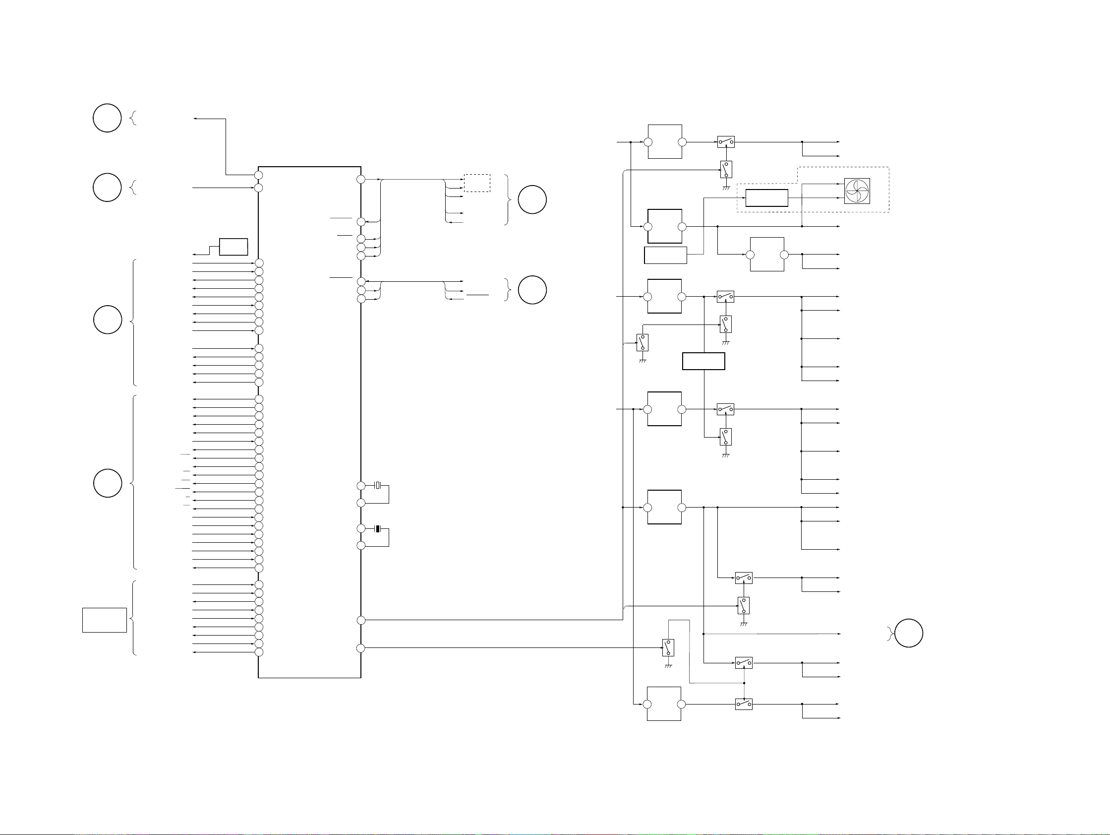
7-1. CIRCUIT BOARDS LOCATION
d
HCD-DR7AV/XB800AV
SECTION 7
DIAGRAMS
TC-A board
PANEL FL board
PANEL VR board
SURROUND AMP board
TC-B board
FRONT INPUT board
LED (PANEL) board
TUNER UNIT
JACK board
SUB TRANS board
(XB800AV)
TRANS board
MAIN boar
LEAF SW board
AUDIO board
CD MOTOR board
CD-L board
DOOR SWITCH board
TABLE SENSOR board
BD board
CD-R board
PA board
LED (CD) board
– 19 –
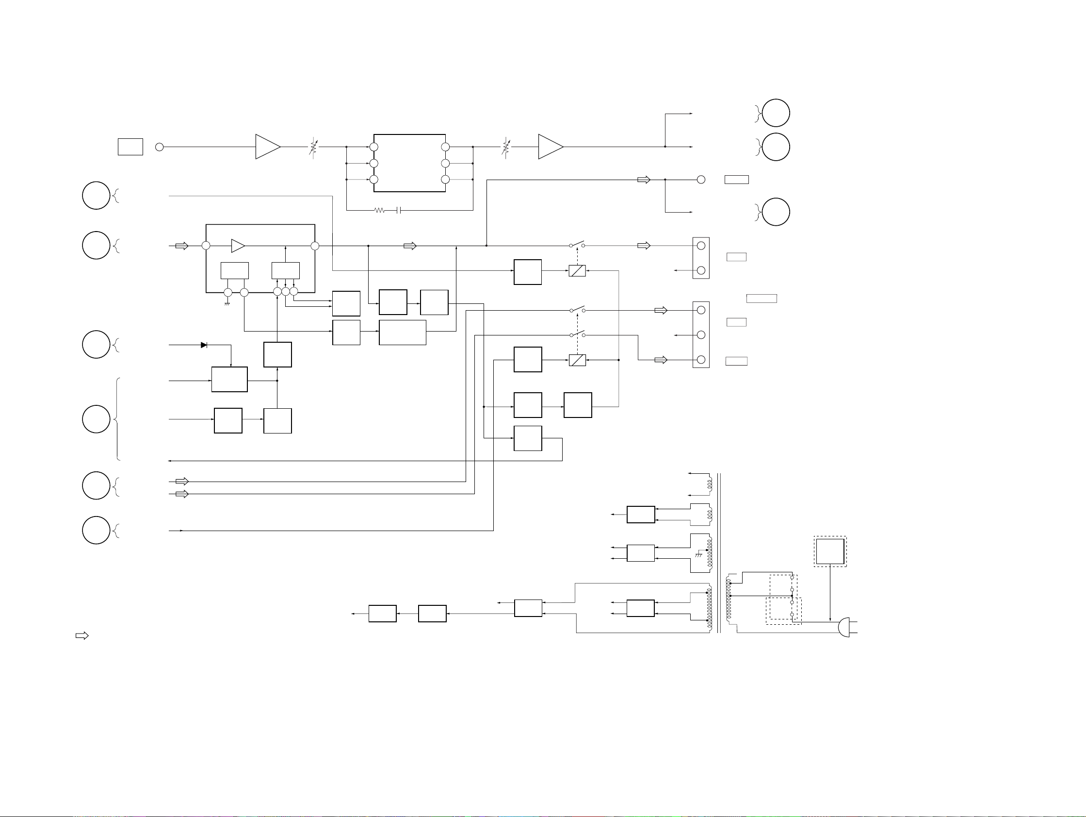
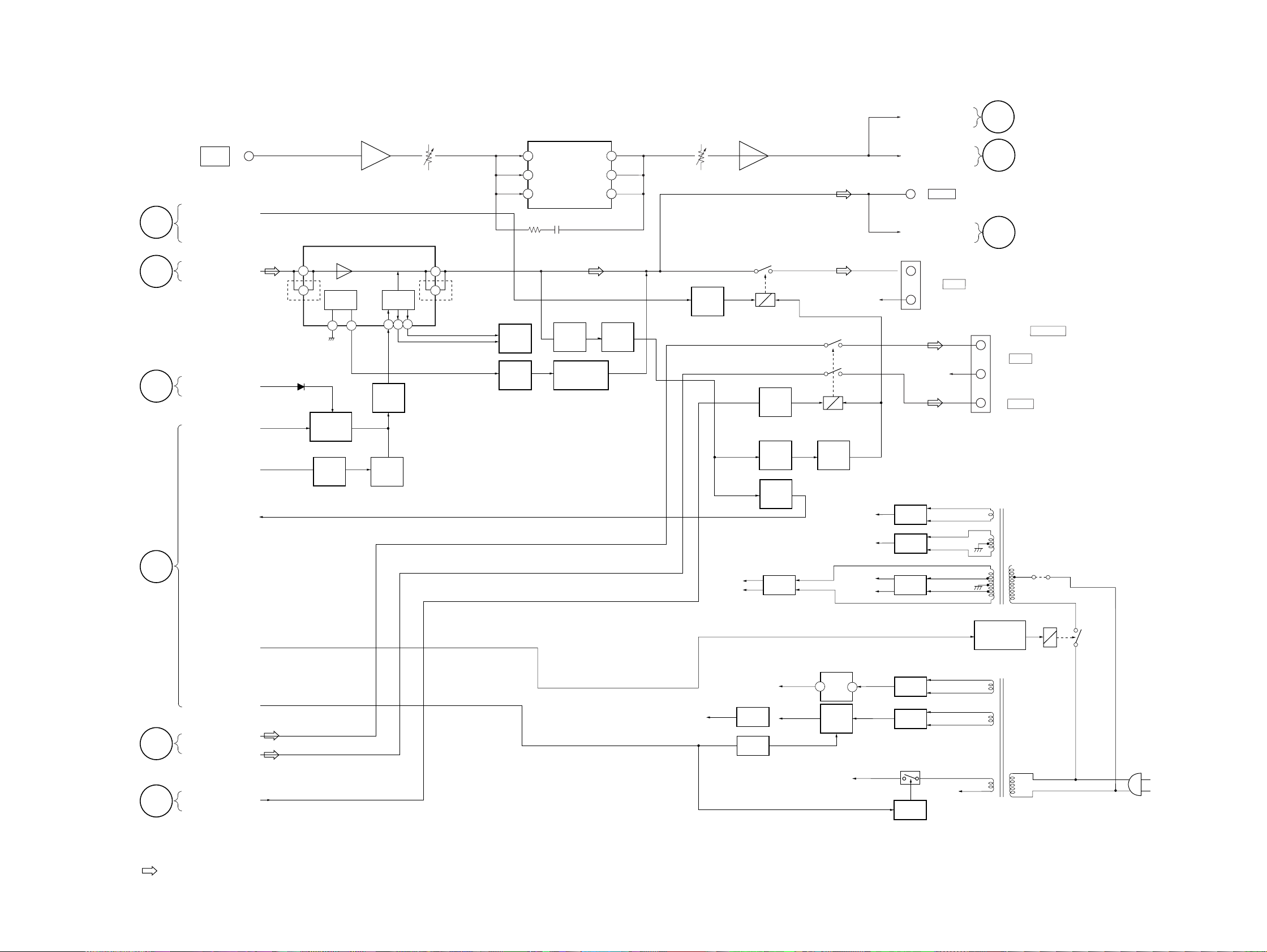
Page 20
HCD-DR7AV/XB800AV
7-2. BLOCK DIAGRAMS
– BD (CD) SECTION –
OPTICAL PICK-UP BLOCK
(KSS-213B/K-N)
DETECTOR
E
A
LASER
DIODE
LD
POWER
SPINDLE
M102
SLED
MOTOR
M101
MOTOR
C
D
B
E
F
M
M
• SIGNAL PATH
: CD
: Digital out
09
ABC
D
F
FD
PD
TRACKING
COIL
FOCUS
COIL
VCC
VC
SD+
SD–
SP+
SP–
LD
DRIVE
Q101
T+
T–
F+
F–
A
5
C
7
D
8
B
6
E
11
F
10
LD
3
PD
4
VREF
IC102
FOCUS/TRACKING COIL DRIVE
SPINDLE/SLED MOTOR DRIVE
CH2OUTR
11
CH2OUTF
12
CH1OUTF
14
CH1OUTR
13
CH3OUTF
17
CH3OUTR
18
CH4OUTF
15
CH4OUTR
16
CH2FIN
CH2RIN
CH1FIN
CH1RIN
CH3RIN
CH3FIN
CH4SIN
CH4BIN
MUTE
SUMMING
TRACKING
APCLD/PD
AMP
5
6
2
3
23
24
25
27
20
IC103
RF AMP
RF
AMP
FOCUS
ERROR
AMP
ERROR
AMP
TFDR
TRDR
FFDR
FRDR
SRDR
SFDR
BUFFER
HOLD SW
VC
VC
RF EQ
AMP
REF
RF
16
FF
14 49
TE
13
12
VC
LDON
22
1521
INTEGRATOR
INTEG-
RATOR
VC
IC101
DIGITAL SERVO
DIGITAL SIGNAL PROCESSOR
RF AC
51
ASY1
ASYMMETRY
CORRECTION
ASY0
48
VC
38
CE
42
RFDC
43
FE
TE
SE
CE
TFDR
TRDR
FFDR
FRDR
SRDR
SFDR
MDP
OPERATIONAL
AMPLIFIER
ANALOG
SWITCH
PWM
GENERATOR
TRACKING
PWM
GENERATOR
FOCUS
PWM
GENERATOR
SLED
PWM
GENERATOR
DIGITAL
CLV
39
41
40
42
30
31
32
33
29
28
26
DIGITAL
PLL
A/D
CONVERTER
SERVO DSP
TRACKING
SERVO
FOCUS
SERVO
SLED
SERVO
16K
RAM
EFM
DEMODULATION
SUBCODE
PROCESSOR
SERIAL IN
INTERFACE
OVER SAMPLING
DIGITAL FILTER
3rd ORDER
NOISE SHAPER
PWM PWM
DATA BUS
ERROR
CORRECTOR
D/A
INTERFACE
SERVO
AUTO
SEQUENCER
TIMING
LOGIC
DIGITAL
OUT
CPU
INTERFACE
SERVO
INTERFACE
XTA1
STAO
D OUT
XRST
SQSO
SQCK
SENS
DATA
XLAT
CLOK
SCOR
XLON
SCLK
SSTP
RMUT
LMUT
LMUT
AIN1
LOUT1
LOUT2
AIN2
LOUT2
66
67
60
3
1
2
8
5
6
7
20
14
9
27
79
80
70
71
72
77
76
75
S101
LIMIT SW
X101
16.9344MHz
DOUT
XRST
SQSO
SENS
DATA
XLT
CLOK
SCOR
SQCK
+5V
L OUT
R OUT
HOLD
A
MAIN
SECTION
(Page 25, 27)
– 21 – – 22 –
Page 21
– DECK SECTION –
HCD-DR7AV/XB800AV
HP101
PB HEAD
(DECK A)
REC/PB HEAD
(DECK B)
HRPE101
ERASE HEAD
PB A/B
MS OUT
TC PB L
LM ON/OFF
NORM/HIGH
NR ON/OFF
REC/PB/PASS
TC REC L
BIAS ON/OFF
RM ON/OFF
ALC ON/OFF
RELAY
CAPM CNT1
CAPM CNT2
CAP M H / L
A SHUT
B
MAIN
SECTION
(Page 25,
26, 27)
17
2
DOLBY NR
RECOUT
D
32
S1008
B CrO
2
19
B NORM/CROM/
METAL
PAS
DOL
BIAS SW
M
31, 33
M1
CAPSTAN
MOTOR
DOLBY
TYPE B
CN301
1
R CH
28
27
M
MS
26
PB OUT
LM ON/
OFF
NORM/
HIGH
NR ON/
OFF
PB
LIN
BIAS ON/OFF
RM ON/OFF
ALC ON/OFF
CAP MOTOR
CONTROL
Q336-343
CONTROL
RV1002
NORMAL
SPEED
SPEED
Q1001
40
25
18
23
24
43
20
22
15
RV1001
HIGH
SPEED
3
SWITCH
Q335
REEL
DETECT
IC1001
S1004
A CrO
RV311
4
PLAYBACK
LEVEL
DECK A
RV301
PLAYBACK
LEVEL
DECK B
RV341
REC
BIAS
REC BIAS
BIAS OSC
T621, Q621, 622
IC611
L
R
L
R
X
R CH
R CH
3
P
ERASE BIAS
IC601
1
IC602
R
REC/PB
16
PB-A/B
A IN
48
B IN
46
RV301
REC LEVEL
+7.5V
Q623
EQIN
38
EQOUT
36
A 120/70
70
120
DOLBY NR
IC301
39
REEL
DETECT
IC1002
S1001 (A PLAY)
• R CH : Same as L ch
• SIGNAL PATH
+5V
S1002 (B PLAY)
: PB (DECK A)
: PB (DECK B)
: REC (DECK B)
09
• PLUNGER SOLENOID is supplied
as the MECHANICAL BLOCK ASSY.
A DECK/
B DECK
PLUNGER
TRIGGER
MOTOR
CONTROL
Q331-334
S1003
(A HALF)
S1005
(REC A)
S1006
(B HALF)
S1009
(REC B)
+5V
+5V
B SHUT
A PLAY
B PLAY
A HALF
B HALF/REC A/REC B
B TRIG
A TRIG
– 23 –
– 24 –
Page 22
HCD-DR7AV/XB800AV
– MAIN (1/2) SECTION –
VIDEO 2
IN
VIDEO
IN
PHONO
(L IN)
FM/AM TUNER
TUNER UNIT IS
SUPPLED AS THE
ASSEMBLED
BLOCK
DECK
SECTION
(Page 24)
CD
SECTION
(Page 22)
POWER
SECTION
(Page 30,
B
A
C
32)
MD (L IN)
R, AUDIO
(L IN)
V2, AU,
L-CH IN
FRONT
(L IN)
TC PB L
MIC-SIG
J804
J702
J701
ST-L
CD-L
J701
J701
J804
J703
IC191
AV SWITCH
6
IN3
IN4
IN1
1
B
A
2 3 5
46 45 28
IC181 SELECTOR
12
X0
X1
14
15
X2
A
10 9
46 45
X
B
VD OUT
13
J702
SPEANA
J701
L-CH SIG
TC REC L
IC101
AF AMP
VIDEO
OUT
REC OUT
D
E
(Page 29, 31)
B
6
7
DISPLAY
SECTION
(Page 33)
POWER
SECTION
DECK
SECTION
(Page 24)
REAR-L
CENTER
M
POWER
SECTION
(Page 29, 31)
10
IC101
C
IC601
PHONO AMP
3
1
SOUND PROCESSOR 1
L+R
69
IN A2
IN B2
68
IN C2
67
IN D2
66
65
IN E2
MIC IN
2
64
IN F2
59 60
B OUT 2 IN F2
REC B2
BUS OUT2
REC A2
BBA2
BBB2
BUF IN2
30
57
36
SWITCH
Q111
TC REC L
SWITCH
Q112
(TA-MUTE)
7
58
39
38
37
SWITCH
Q114
SWITCH
Q115
44 34
MUTE
SWITCH
Q113
10
14
MAIN CONTROL
IC501 (1/2)
7
PL-CLK
PL-DATA
PL-LAT
V-MUTE
493-LAT
7
23
23
24
24
25
25
28
28
34
34
38
38
44
44
45
45
46
46FUNC-SEL0
47
47
48
48493-MUTE
22AC-CUT
RESET
F-RELAY
G
F
DISPLAY
SECTION
(Page 33)
POWER
SECTION
(Page 29, 31)
• R CH: Same as L ch
• SIGNAL PATH
: FM
: CD
: PB
: REC
: VIDEO/MD
– 26 –
74
09
1
11
5
IC201
SOUND PROCESSOR 2
10
TRIM
4
TRIM
VOL
VOL
DATA
SCK
REQ
9
3
24
22
23
23
25
24
MUTE
SWITCH
Q281
MUTE
SWITCH
Q271
(TA-MUTE)
MUTE
SWITCH
Q803
D807
RESET
SWITCH
Q802
MUTE
SWITCH
Q804
6
3
LINE-MUTE
F-RELAY
DBFB-H/L
SW-MODE
BASS FREQ
FUNC-SEL1
493-DATA
– 25 –
Page 23
– MAIN (2/2) SECTION –
HCD-DR7AV/XB800AV
N
POWER
SECTION
(Page 29, 31)
H
POWER
SECTION
(Page 30, 32)
A
BD (CD)
SECTION
(Page 22)
B
DECK
SECTION
(Page 24)
FM/AM TUNER
TUNER UNIT IS
SUPPLED AS THE
ASSEMBLED
BLOCK
PL-RELAY
HP.SW
SCOR
SQ-DATA
SQ-CLK
CD-DATA
CD-CLK
SENS
HOLD
X-LAT
X-RST
TRAY.SENS
TBL.L
TBL.R
UP SW
LED
B TRG
A TRG
CAPM-CNT 2
CAPM-CNT 1
CAP-M-H/L
MS OUT
LM ON/OFF
REC/PB/PASS
NR ON/OFF
RM ON/OFF
BIAS ON/OFF
NORM/HIGH
PB A/B
ALC ON/OFF
B PLAY
A PLAY
A-HALF
B-HALF/REC A/REC B
B SHUT
A SHUT
RELAY
RDS-INT
RDS-DATA
ST-MUTE
STEREO
TUNED
ST-CE
ST-DOUT
ST-DIN
ST-CLK
IC781
OPTIC
TRANSMITTING
D.OUT
4
PL-RELAY
H/P IN
36
SCOR
19
SQ-DATA
32
SQ-CLK
33
CD-DATA
35
CD-CLK
37
SENS
56
HOLD
57
XLT
58
XRST
59
61
DISC-SENS
63
TBL-L
65
TBL-R
68
ENC 3/UP-SW
ENC 2/DISC-LED
69
72
B-TRG
73
A-TRG
74
CAPM-CNT 2
75
CAPM-CNT 1
76
CAP-M-H/L
77
AMS IN
78
TC-MUTE
79
R/PB/PAS
80
NR-ON/OFF
REC-MUTE
81
82
BIAS
83
EQ-H/N
84
PB-A/B
ALC
85
86
B-PLAY-SW
87
A-PLAY-SW
88
A-HALF
89
B-HALF
90
B-SHUT
91
A-SHUT
TC-RELAY
100
20
RDS-INT
21
RDS-DATA
49
ST-MUTE
50
STEREO
51
TUNED
52
ST-CE
53
ST-DOUT
54
ST-DIN
55
ST-CLK
MAIN CONTROL
IC501 (2/2)
STK-POWER
STBY RELAY
PROTECT
FL OFF
HP MUTE
WAKE UP
IIC-CLK
IIC-DATA
XC-IN
XC-OUT
X-OUT
X-IN
POWER
CD-POWER
1
27
42
43
93
18
29
30
32.768kHz
10
11
13
15
2
5
1
27
42
43
93
18
29
30
X501
X502
16MHz
43
42
93
1
27
30
29
18
XB800AV
ONLY
POWER
ECO
HP MUTE
STK POWER
PROTECT
DATA
CLOCK
WAKE UP
I
POWER
SECTION
(Page 29, 31)
J
DISPLAY
SECTION
(Page 33)
+UNREG, 12V
UN–10V
UN+10V
2
IC931
+10V
1 3
REG
IC932
+12V
1 3
REG
FAN DETECTOR
D405-409
IC951
–7V
2 3
REG
Q932
SWITCH
IC901
+7V
1 3
REG
IC911
+5V
1 3
REG
Q914
SWITCH
5
IC921
DETECTOR
Q905
SWITCH
2
SWITCH
SWITCH
2
Q931
Q931
Q901
Q932
SWITCH
Q932
SWITCH
Q902
SWITCH
SWITCH
2
SWITCH
Q901
Q913
FAN SWITCH
Q961, 963
IC933
+7V
1 3
REG
Q902
SWITCH
(LED–7V)
(LED+7V)
(D+5V SW)
(CD D+5V SW)
(CD A+5V SW)
PL A+10V
ST +10V
FAN901
FAN
TC MOTOR+12V
M+7V (UNSW)
7V
A–7.5V
–V BIAS
–7
TC–7V
–7V
A+7.5V
+V BIAS
–7
TC–7V
–7V
LED 5V
LED 5V
D+5V UNSW
5V
AU D+5V
EVER +5V
D+5V (SW)
A+5V (SW)
DR7AV
POWER
SECTION
L
(Page 29, 31)
+5V
1 3
REG
09
• R CH : Same as L ch
Q921
SWITCH
CD D+5V SW
CD A+5V SW
– 27 – – 28 –
Page 24
HCD-DR7AV/XB800AV
– POWER SECTION – (DR7AV model)
MAIN 1
SECTION
(Page 26)
MAIN 1
SECTION
(Page 26)
MAIN 2
SECTION
(Page 28)
MAIN 2
SECTION
(Page 27)
MAIN 1
SECTION
(Page 26)
G
E
L
I
M
MIX MIC
J801
F-RELAY
L-CH IN
EVER +5V
HP-MUTE
STK-POWER
PROTECT
REAR-L
CENTER
POWER AMP & VOLUME CONTROL
22
THERMAL
SENSOR
13
12
D804
HEAD PHONE
MUTE
Q833
MUTE
DRIVE
Q804
MIC AMP
IC850 (1/2)
IC801
CONTROL
SWITCH
VOLUME
CONTROL
8
MUTE
Q834
MUTE
Q803
6
5
MIC VOLUME
RV850
15
VOLUME
CONTROL
D802, 852
THERMAL
SENSOR
Q831-832
ECHO CONTROL
9
LPF 2 IN
OP 2 IN
11
1
LPF 1 IN
PROTECT
DC AMP
Q433-434
L-CH THERMAL
PROTECT SWITCH
Q801
IC851
LPF 1 OUT
LPF 2 OUT
OP 2 OUT
LATCH
DRIVER
Q432
DISPLAY
SECTION
(Page 33)
MAIN 1
SECTION
(Page 25)
MAIN 2
SECTION
(Page 27)
VF
VF
MIC-SIG
MIC-SIG
J803
HP.SW
TM401
TM402
POWER
TRANSFORMER
T951
PHONES
L
FRONT
R
L
REAR
R
CENTER
MIC LEVEL
RV851
2
8
10
RELAY
DRIVER
Q401-402
RELAY
DRIVER
Q403, 407
LATCH
DRIVER
Q437
PROTECT
SWITCH
Q439
MIC AMP
IC850 (2/2)
RY401
RY402
PROTECT
SWITCH
Q431
R-CH
R-CH
K
C
H
SURROUND
09
MAIN 2
SECTION
(Page 29)
• R CH : Same as L ch
• SIGNAL PATH
: FM
N
PL-RELAY
VF (–35V)
SWITCH
Q904
–35V REG
Q903
+VH
RECT
D831
+UNREG. 12V
UN +10V
UN –10V
AC-L
AC-L
RECT
D833-836
RECT
D841-844
RECT
D832
JW969
JW968
AUS ONLY
TH ONLY
SP, EA
VOLTAGE
SELECTOR
VS901
AC
IN
– 29 – – 30 –
Page 25
– POWER SECTION – (XB800AV model)
J801
MIX MIC
MIC AMP
IC850 (1/2)
MIC VOLUME
RV850
9
11
1
LPF 2 IN
OP 2 IN
LPF 1 IN
ECHO CONTROL
IC851
LPF 1 OUT
LPF 2 OUT
OP 2 OUT
HCD-DR7AV/XB800AV
DISPLAY
MIC LEVEL
RV851
2
8
10
MIC AMP
IC850 (2/2)
MIC-SIG
MIC-SIG
J803
PHONES
K
C
SECTION
(Page 33)
MAIN 1
SECTION
(Page 25)
MAIN 1
SECTION
(Page 26)
MAIN 1
SECTION
(Page 26)
MAIN 2
SECTION
(Page 28)
MAIN 2
SECTION
(Page 27)
G
E
L
I
F-RELAY
L-CH IN
EVER +5V
HP-MUTE
STK-POWER
PROTECT
XB800AV
POWER AMP & VOLUME CONTROL
22
14
THERMAL
SENSOR
13
12
D804
HEAD PHONE
MUTE
Q833
MUTE
DRIVE
Q804
IC801
VOLUME
CONTROL
8
MUTE
CONTROL
Q834
MUTE
SWITCH
Q803
MAIN 2
HP.SW
RY401
15
XB800AV
7
6
5
VOLUME
CONTROL
D802, 852
THERMAL
SENSOR
Q831-832
PROTECT
DC AMP
Q433-434
L-CH THERMAL
PROTECT SWITCH
Q801
LATCH
DRIVER
Q432
RELAY
DRIVER
Q401-402
+VH
–VH
RELAY
DRIVER
Q403, 407
LATCH
DRIVER
Q437
PROTECT
SWITCH
Q439
RECT
D831
RY402
PROTECT
SWITCH
Q431
+UNREG. 12V
R-CH
+UN 10V
+VL
–VL
TM401
RECT
D833-836
RECT
D841-844
RECT
D832
L
FRONT
R
R-CH
H
TM402
POWER
TRANSFORMER
SECTION
(Page 27)
SURROUND
L
REAR
R
CENTER
T951
JW954
MAIN 1
SECTION
(Page 26)
MAIN 2
SECTION
(Page 27)
09
M
N
• R CH : Same as L ch
• SIGNAL PATH
: FM
POWER
ECO
REAR-L
CENTER
PL-RELAY
SUB-TRANSFORMER
+5.6V
VF
–30V REG
Q903
SWITCH
Q907
3
SWITCH
+5.6V
REG
IC901
POWER
Q902
1
VF
RECT
D902-905
RECT
D907-910
SWITCH
Q904-905
SWITCH
Q906
VF
– 31 – – 32 –
STANDBY
RELAY CONTROL
Q901
T901
STANDBY
RELAY
RY901
AC
IN
Page 26
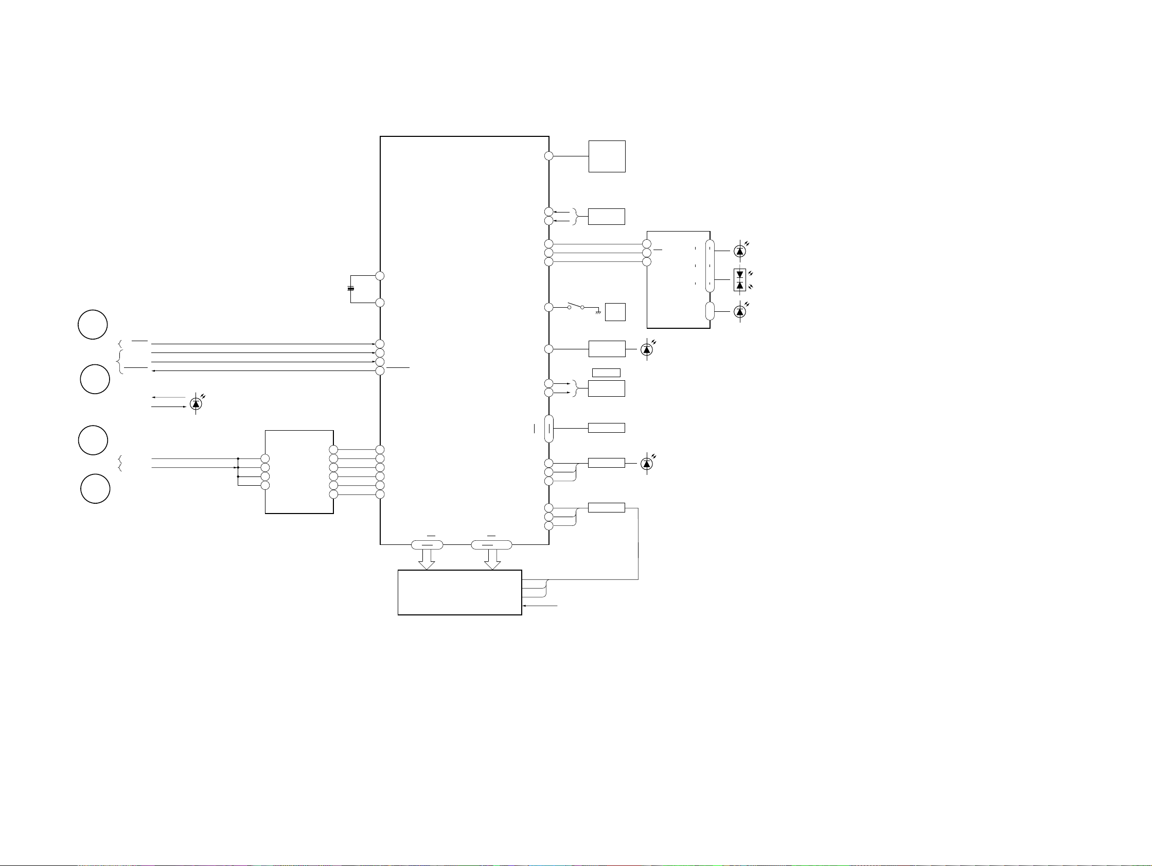
HCD-DR7AV/XB800AV
– DISPLAY SECTION –
(Page
F
26)
RESET
DATA
CLOCK
WAKE UP
A –7V
A +7V
(Page
27)
MAIN 1 SECTION
MAIN 2 SECTION
J
(Page 30, 32)
K
POWER SECTION
MAIN 1 SECTION
MIC–SIG
SPE–ANA
D
(Page 26)
D671 – D675
X601
12.5MHz
REC LEVEL
OUTPUT
DISPLAY CONTROL (FOR MIC)
IC603
LINE NF
LINE IN
REC IN
REC NF
REC LEVEL
F06
F05
F04
F02
F01
3
4
6
5
DISPLAY CONTROL
IC601
REMOTE
1
SIRCS
2
JOG A
8
JOG B
3
LED SCK
LED DAT
D-SW
LED SEL
KEY 0
KEY 4
REC LED
LED-EC0
GR-1
GR-15
GR-16
4
5
80
7
9
10
11
15
74
75
77
43
28
27
LED LATCH
70
X IN
X OUT
72
73
RESET
2
78
I
C DATA
2
79
I
C CLK
22
WAKE UP
VOLUME A
VOLUME B
11
12
13
14
16
17
21
20
19
18
17
16
ALL BAND
BPF 4
BPF 3
BPF 2
BPF 1
BPF 0
SEG-1
45 67
DAILY LED
23
GR-3 14, 2
29VF40, 42
CONTROL
RECIEVE
IC602
S702
JOG
ROTARY
ENCODER
S691
6
OPEN
Q601 – Q603
LED POWER
SWITCH
S701
VOLUME
ROTARY
ENCODER
KEY MATRIX
Q605 – Q607
LED DRIVER
Q608 – Q610
DRIVER
14
CLK
15
STB
13
DATA
D604 – D607
D604 – D607
D601 – D603
SERIAL
PARALLEL
CONVERTER
IC604
D611 – D613, D616 – D621,
D623 – D627, D635 – D638
1
P3
5
P5
•
•
7
P7
9
P11
•
•
20
P12
22
P14
P1
17
•
•
P2
19
D700
D631, D632
FLUORESCENT INDICATOR TUBE
09
FL601
– 33 – – 34 –
Page 27
HCD-DR7AV/XB800AV
2.5V
APPROX 500mVp-p (PLAY)
2.5V
APPROX 200m Vp-p (PLAY)
THIS NOTE IS COMMON FOR PRINTED WIRING
BOARDS AND SCHEMATIC DIAGRAMS.
(In addition to this, the necessary note is printed
in each block.)
For schematic diagrams.
Note:
• All capacitors are in µF unless otherwise noted. pF: µµF
50 WV or less are not indicated except for electrolytics
and tantalums.
• All resistors are in Ω and 1/
specified.
¢
•
• C : panel designation.
Note: The components identified by mark ! or dotted
• U : B+ Line.
• V : B– Line.
• H : adjustment for repair.
• Voltages and wavefor ms are dc with respect to ground
• Voltages are taken with a VOM (Input impedance 10 MΩ).
• Waveforms are taken with a oscilloscope.
• Circled numbers refer to wavefor ms.
• Signal path.
• Abbreviation
: internal component.
line with mark ! are cr itical for safety.
Replace only with part number specified.
under no-signal (detuned) conditions.
Voltage variations may be noted due to normal produc-
tion tolerances.
Voltage var iations may be noted due to nor mal pro-
duction tolerances.
F : FM
g : VIDEO/MD
E : PB (DECK A)
d : PB (DECK B)
G : REC (DECK B)
J : CD
c : digital out
I : PHONO
EA : Saudi Arabia model.
AUS : Australian model.
SP : Singapore model.
TH : Thai model.
4
W or less unless otherwise
WAVEFORMS
– BD (CD) SECTION –
1
16.9MHz
IC101 ^§ XTAI
2
(PLAY)
IC101 %¡ RF AC
3
IC101 $¡ TE
4
IC101 #ª FE
5
7.5µsec
IC101 @§ MDP
3.1Vp-p
1.2Vp-p
2.4Vp-p
– MAIN (2/5) SECTION –
1
5.5Vp-p
16MHz
IC501 !£ X-OUT
2
5.2Vp-p
32.768kHz
IC501 !¡ XC-OUT
– PANEL FL SECTION –
1
3.4Vp-p
12.5MHz
IC601 &™ X-OUT
For printed wiring boards.
Note:
• X : parts extracted from the component side.
•
•
• b : Pattern from the side which enables seeing.
(The other layers' patterns are not indicated.)
• Indication of transistor
®
: Through hole.
¢
: internal component.
C
EB
These are omitted
C
Q
These are omitted
EB
– 35 –
– 36 –
Page 28

HCD-DR7AV/XB800AV
7-3. PRINTED WIRING BOARD – BD (CD) SECTION –
• See page 19 for Circuit Boards Location.
(VC)
(RP)
(AGCCON)
(FE)
(TE)
(FF1)
(Page 42)
19
Q
– 37 –
– 38 –
Page 29

7-4. SCHEMATIC DIAGRAM – BD (CD) SECTION –
• See page 36 for Waveforms.
HCD-DR7AV/XB800AV
TP
(TE)
TP
(FE)
TP
(RP)
C
(Page 48)
220
19P
NC
TP (AGCCON)
(VC)
TP
68
10V
– 39 – – 40 –
Page 30

HCD-DR7AV/XB800AV
• Semiconductor
Location
Ref. No. Location
D333 I-3
D334 I-3
D335 I-4
D336 I-4
D501 I-6
D534 G-7
D544 G-7
D802 H-8
D803 H-8
D804 H-7
D805 H-8
D806 H-7
D807 I-9
D808 I-6
D911 E-10
D912 F-9
D913 F-10
D931 G-10
D951 B-11
IC101 D-3
IC201 C-9
IC181 B-5
IC191 B-7
IC301 G-3
IC501 H-6
IC601 A-1
IC901 C-11
IC931 G-10
IC932 G-11
IC933 H-11
IC951 B-11
IC801 I-8
IC911 E-10
7-5. PRINTED WIRING BOARD – MAIN SECTION –
• See page 19 for Circuit Boards Location.
(Page 101)
(Page 84)
Q111 D-5
Q112 D-5
Q113 D-5
Q115 D-4
Q161 E-5
Q162 E-5
Q163 E-5
Q165 E-3
Q271 C-7
Q281 C-7
Q331 I-2
Q332 I-2
Q333 I-2
Q334 I-2
Q335 I-4
Q336 I-3
Q337 I-3
Q338 I-4
Q339 I-4
Q340 I-3
Q341 I-3
Q342 I-3
Q343 I-3
Q801 H-7
Q802 I-9
Q803 I-8
Q804 I-8
Q901 C-11
Q902 B-11
Q903 B-11
Q904 B-11
Q905 B-11
Q906 B-11
Q911 F-9
Q912 F-9
Q913 F-9
Q914 F-9
Q931 G-10
Q932 G-9
Q961 A-10
Q962 A-10
(Page 91)
(Page 55)
(Page 100)
(Page 61,
63)
(Page 61,
63)
(Page
87)
(Page
38)
(Page 71)
– 41 –
– 42 –
Page 31

7-6. SCHEMATIC DIAGRAM – MAIN (1/5) SECTION –
• See page 103 for IC Block Diagrams.
HCD-DR7AV/XB800AV
(Page
52)
(Page
82)
(Page
47)
(Page
50)
(Page
45, 46)
– 43 – – 44 –
(Page
101)
(Page
51)
Page 32

HCD-DR7AV/XB800AV
7-7. SCHEMATIC DIAGRAM – MAIN (2/5) SECTION –
• See page 36 for Waveforms.
• See page 41 for Printed Wiring Board.
• See page 104 for IC Pin Functions.
(Page 51)
(Page 44)
(Page 52)
(Page
50)
(Page 70)
– 45 –
(Page 47, 48)
(Page 48)
– 46 –
Page 33

7-8. SCHEMATIC DIAGRAM – MAIN (3/5) SECTION –
• See page 41 for Printed Wiring Board.
HCD-DR7AV/XB800AV
(Page 45, 46)
(Page 46)
(Page 49)
(Page 39)
(Page 86)
(Page
51)
(Page 44)
– 47 – – 48 –
Page 34

HCD-DR7AV/XB800AV
7-9. SCHEMATIC DIAGRAM – MAIN (4/5) SECTION –
• See page 41 for Printed Wiring Board.
(Page 44)
(Page 54)
(Page 100)
(Page 51)
(Page 47)
– 49 –
(Page 45)
– 50 –
Page 35

7-10. SCHEMATIC DIAGRAM – MAIN (5/5) SECTION –
• See page 41 for Printed Wiring Board.
(Page
48)
HCD-DR7AV/XB800AV
(Page
45)
(Page
49)
(Page
44)
(Page 90)
(Page 44)
(Page 46)
(Page 57, 65)
(Page 57, 65)
– 51 – – 52 –
Page 36

HCD-DR7AV/XB800AV
7-11. SCHEMATIC DIAGRAM – DECK SECTION –
(Page 49)
– 53 –
– 54 –
Page 37

7-12. PRINTED WIRING BOARD – DECK SECTION –
• See page 19 for Circuit Boards Location.
HCD-DR7AV/XB800AV
(Page 41)
– 55 – – 56 –
Page 38

HCD-DR7AV/XB800AV
7-13. SCHEMATIC DIAGRAM – POWER (1/2) SECTION – (DR7AV model)
• See page 61 for Printed Wiring Board.
(Page 97)
(Page 52)
(Page 52)
(Page 89)
– 57 –
(Page 59)
(Page 59)
(Page 60)
– 58 –
Page 39

7-14. SCHEMATIC DIAGRAM – POWER (2/2) SECTION – (DR7AV model)
• See page 61 for Printed Wiring Board.
HCD-DR7AV/XB800AV
(Page 57)
(Page 57)
(Page 58)
(Page 102)
– 59 – – 60 –
Page 40

HCD-DR7AV/XB800AV
7-15. PRINTED WIRING BOARD – POWER SECTION – (DR7AV model)
• See page 19 for Circuit Boards Location.
SORROUND SPEAKER
REAR
CENTER
• Semiconductor
Location
Ref. No. Location
D401 G-4
D402 C-2
D403 E-8
D405 A-1
D406 B-1
D801 F-4
D802 E-5
D803 E-6
D823
D831 I-8
D833 I-5
D834 I-5
D835 I-5
D836 I-5
D841 I-3
D842 I-2
D843 I-3
D844 I-3
D851 F-4
D852 E-5
D911 I-9
D912 I-8
(Page 42)
(Page 42)
IC801 D-4
Q401 C-1
Q402 C-1
Q403 E-8
Q407 E-8
Q431 F-8
Q432 G-8
Q433 G-8
Q434 G-7
Q437 G-8
Q439 G-8
Q801 F-4
Q803 F-6
Q804 F-6
Q805 H-3
Q831 F-2
Q832 F-2
Q833 G-2
Q834 F-3
Q851 F-4
Q855 H-3
Q903 I-9
CN805
(Page 91)
– 61 –
(Page 99)
(Page 101)
– 62 –
Page 41

7-16. PRINTED WIRING BOARD – POWER SECTION – (XB800AV model)
• See page 19 for Circuit Boards Location.
SORROUND SPEAKER
REAR
CENTER
HCD-DR7AV/XB800AV
• Semiconductor
Location
Ref. No. Location
D401 G-4
D402 C-2
D403 E-8
D405 A-1
D406 F-4
D801 F-4
D803 E-6
D804 G-2
D805 E-3
D831 I-8
D833 I-5
D834 I-5
D835 I-5
D836 I-5
D841 I-3
D842 I-2
D843 I-3
D844 I-3
D851 F-4
D902 G-9
D903 G-9
D904 G-9
D905 G-9
D906 H-9
D907 G-9
D908 H-9
D909 H-9
D910 G-9
D911 I-9
D912 I-8
D913 I-9
(Page 42)
(Page 42)
CN805
(Page 96)
IC801 D-4
IC901 H-9
Q401 C-1
Q402 C-1
Q403 E-8
Q407 E-8
Q431 F-8
Q432 G-8
Q433 G-8
Q434 G-7
Q437 G-8
Q439 G-8
Q801 F-4
Q803 F-6
Q804 F-6
Q805 H-3
Q831 F-2
Q832 F-2
Q833 G-2
Q834 F-3
Q851 F-4
Q855 H-3
Q901 G-10
Q902 H-9
Q903 I-9
Q904 I-8
Q905 I-8
Q906 I-9
Q907 I-9
(Page 91)
(Page 95)
(Page 101)
– 63 – – 64 –
Page 42

HCD-DR7AV/XB800AV
7-17. SCHEMATIC DIAGRAM – POWER (1/2) SECTION – (XB800AV model)
• See page 63 for Printed Wiring Board.
(Page 93)
(Page
52)
(Page
52)
(Page
89)
– 65 –
(Page 67)
(Page 68)
– 66 –
Page 43

7-18. SCHEMATIC DIAGRAM – POWER (2/2) SECTION – (XB800AV model)
• See page 63 for Printed Wiring Board.
HCD-DR7AV/XB800AV
(Page 94)
(Page 65)
(Page 66)
(Page 102)
– 67 – – 68 –
Page 44

HCD-DR7AV/XB800AV
7-19. SCHEMATIC DIAGRAM – PANEL FL SECTION –
• See page 103 for IC Block Diagrams.
• See page 106 for IC Pin Functions.
(Page 77)
(Page
78)
(Page 77)
(Page 46)
– 69 –
(Page 73)
– 70 –
Page 45

7-20. PRINTED WIRING BOARD – PANEL FL SECTION –
• See page 19 for Circuit Boards Location.
HCD-DR7AV/XB800AV
XB800AV
(Page 41)
• Semiconductor
Location
Ref. No. Location
D601 A-13
D602 C-13
D603 C-13
D604 C-5
D605 D-6
D606 A-1
D607 A-3
D608 D-2
IC601 D-9
IC602 C-4
IC603 E-12
(Page 79)
Ref. No. Location
IC604 E-4
Q601 D-2
Q602 C-2
Q603 D-2
Q605 A-12
Q606 E-13
Q607 F-13
Q608 D-10
Q609 C-10
Q610 C-9
(Page 80)
(Page 79)
(Page 75)
– 71 – – 72 –
Page 46

HCD-DR7AV/XB800AV
7-21. SCHEMATIC DIAGRAM – PANEL VR SECTION –
• See page 103 for IC Block Diagrams.
(Page 70)
– 73 –
– 74 –
Page 47

7-22. PRINTED WIRING BOARD – PANEL VR SECTION –
(Page 71)
PRO
LOGIC
DSP
DSP
• See page 19 for Circuit Boards Location.
HCD-DR7AV/XB800AV
• Semiconductor
Location
Ref. No. Location
D611 B-5
D612 C-4
D613 D-5
D616 D-9
D617 D-10
D618 D-11
D619 B-8
D620 B-8
D621 C-8
D623 C-9
D624 C-9
D625 C-10
D626 C-11
D627 C-11
– 75 – – 76 –
Page 48

HCD-DR7AV/XB800AV
7-23. SCHEMATIC DIAGRAM – TC PANEL SECTION –
(Page 70)
(Page 70)
(Page 82)
(Page 69)
(Page 81, 82)
– 77 –
– 78 –
Page 49

7-24. PRINTED WIRING BOARD – TC PANEL SECTION –
• See page 19 for Circuit Boards Location.
(Page 72)
HCD-DR7AV/XB800AV
(Page 71)
(Page 71)
(Page 83)
(Page 84)
– 79 – – 80 –
Page 50

HCD-DR7AV/XB800AV
7-25. SCHEMATIC DIAGRAM – CD PANEL SECTION –
(Page 78)
(Page 77, 78)
– 81 –
(Page 43)
– 82 –
Page 51

7-26. PRINTED WIRING BOARD – CD PANEL SECTION –
• See page 19 for Circuit Boards Location.
(Page 79)
HCD-DR7AV/XB800AV
(Page 80)
(Page
41)
– 83 – – 84 –
Page 52

HCD-DR7AV/XB800AV
7-27. SCHEMATIC DIAGRAM – CD MOTOR SECTION –
(Page 48)
– 85 –
– 86 –
Page 53

7-28. PRINTED WIRING BOARD – CD MOTOR SECTION –
• See page 19 for Circuit Boards Location.
HCD-DR7AV/XB800AV
(Page 42)
– 87 – – 88 –
Page 54

HCD-DR7AV/XB800AV
7-29. SCHEMATIC DIAGRAM – JACK SECTION –
(Page 57, 65)
(Page 52)
– 89 –
– 90 –
Page 55

7-30. PRINTED WIRING BOARD – JACK SECTION –
• See page 19 for Circuit Boards Location.
HCD-DR7AV/XB800AV
(Page 41)
(Page 61, 63)
– 91 – – 92 –
Page 56

HCD-DR7AV/XB800AV
7-31. SCHEMATIC DIAGRAM – TRANS SECTION – (XB800AV model)
(Page 65)
(Page 67)
– 93 –
– 94 –
Page 57

7-32. PRINTED WIRING BOARD – TRANS SECTION – (XB800AV model)
• See page 19 for Circuit Boards Location.
HCD-DR7AV/XB800AV
(Page 64)
(Page
64)
– 95 – – 96 –
Page 58

HCD-DR7AV/XB800AV
7-33. SCHEMATIC DIAGRAM – TRANS SECTION – (DR7AV model)
(Page 57)
– 97 –
– 98 –
Page 59

HCD-DR7AV/XB800AV
7-34. PRINTED WIRING BOARD – TRANS SECTION – (DR7AV model)
• See page 19 for Circuit Boards Location.
SP, EA
SP, EA
7-35. SCHEMATIC DIAGRAM – LEAF SW SECTION –
(Page 49)
(Page
62)
7-36. PRINTED WIRING BOARD – LEAF SW SECTION –
• See page 19 for Circuit Boards Location.
(Page 41)
– 99 – – 100 –
Page 60

HCD-DR7AV/XB800AV
7-37. SCHEMATIC DIAGRAM – SURROUND SECTION –
(Page
44)
7-38. PRINTED WIRING BOARD – SURROUND SECTION –
• See page 19 for Circuit Boards Location.
(Page 59,
67, 68)
(Page 41)
– 101 –
(Page 61, 63)
– 102 –
Page 61

7-39. IC BLOCK DIAGRAMS
2
3
14
1
f04
13
f05
12
f06
11
REC
LEVEL
10
VCC
15
f03
5
REC
NF
6
REC
IN
7
RESET
C
8
BIAS
C
9
GND1
4
16
f02
17
f01
18
RESET
R02
P01
LINE
NF
LINE
IN
REFFERENCE
CURRENT
BPF
DET
BPF
DET
BPF
DET
BPF
DET
DET
RESET
Bias
REFFERENCE
CURRENT
DET
DET
BPF
BPF
• MAIN (1/5) section
IC181 MC14052BF
1
2X0
2X2
2
3
2XCOM
2X3
4
5
2X1
6
INH
7
VEE
VSS
8
IC191 BA7615N
MUTE
LOGIC
8db
75Ω
• PANEL FL section
IC603 BA3830F
16
VDD
15
X2
X1
14
XCOM
13
X0
12
X3
11
A
10
9
B
1
2
3
IN1
CTLB
CTLA
• PANEL VR section
IC851 M65850P
VCC
1/2 VCC
AUTO
RESET
LPF1
2 345 6 7
1
LPF1IN
5
4
IN2
OSCILLATOR
CLOCK
RESET
LPF1OUT
CTLC
CLOCK
D1
6
7
IN3
REF
MAIN
CONTROL
A/D
OP1IN
OP1OUT
VCC
DO0
DO1
CC1
8
OP2IN
IN4
D/A
MO
10
9
IC604 NJU3716L
CTLC
VOUT
DATA
13
CLK
14
VDD
24
OP2OUT
LPF2IN
LPF2OUT
891014 13 12 11
LPF2
20KBIT
SRAM
MI
CC2
GND
STB
15
CLR
16
SHIFT REGISTER
CONTROL
LATCH
17
P1
19
P2
20
P3
21
P4
22
P5
23
P6
P7
1
2
P8
P9
3
P10
4
5
P11
7
P12
8
P13
P14
9
10
P15
11
P16
SO
12
6
GND
18
GND
– 103 –
Page 62

7-40. IC PIN FUNCTIONS
• IC501 MAIN CONTROL (M30622MA-A08FP) (MAIN board)
Pin No.
1 POWER O Power amp ON/OFF signal output
2 POWER O Power ON/OFF signal output
3 F-RELAY O Front speaker relay control output
4 REAR-RELAY O Rear speaker relay control output (Not used)
5 CD-POWER O CD power on signal output
6 LINE-MUTE O Line mute signal output
7 DBFB-H/L O DBFB H/L select signal output
8 – – Connected to ground
9 – – Connected to ground
10 XC-IN I
11 XC-OUT O
12 RESET I System reset signal input
13 X-OUT O X’tal (16MHz) (MAIN SYSTEM CLOCK)
14 VSS – Ground
15 X-IN I X’tal (16MHz) (MAIN SYSTEM CLOCK)
16 VDD – Power supply (+5V)
17 NMI I Not used
18 WAKE UP I WAKE UP signal input
19 SCOR I CD Q-data request signal input
20 RDS-INT I RDS data interrupt input
21 RDS-DATA I RDS data interrupt input
22 AC-CUT I AC cut ON (L)/OFF (H) check
23 PL-CLK O Clock output to pro-logic (Not used)
24 PL-DATA O Data output to pro-logic (Not used)
25 PL-LAT O Latch signal output to pro-logic (Not used)
26 TIMER LED O Not used
27 PROTECT I Speaker protect signal input
28 V MUTE O Video mute signal output
29 IIC-CLK O I2C SCL
30 IIC-DATA O I2C SDA
31 – – Not used
32 SQ-DATA I Subcode Q data clock input (CD data)
33 SQ-CLK I Subcode Q data clock input (CD data clock)
34 SW-MODE O SW-MODE music/movie select signal output
35 CD-DATA O CD data output
36 H/P IN I Head phone detect
37 CD-CLK O CD clock output
38 493-LAT O Latch signal output for IC101 (M62493FP)
39 CLOCK-OUT O Clock out signal check
40 NO-USE – Not used
41 NO-USE – Not used
42 FL OFF O Fluorescent indicator tube filament on/off signal output
43 STBY RELAY O Main POWER on/off signal output
44 BASS FREQ O FREQ high/low signal output (Not used)
45 FUNC SEL 1 O Function select signal output
46 FUNC SEL 0 O Function select signal output
47 493-DATA O Data signal output for IC101 (M62493FP)
48 493-CLK O Clock signal output for IC101 (M62493FP)
49 ST-MUTE O Tuner mute signal output
Pin Name I/O Function
X’tal (32.768 KHz) (SUB CLOCK)
– 104 –
Page 63

Pin No.
50 STEREO I Stereo detection for tuner
51 TUNED I Tuned detection for tuner
52 ST-CE O Tuner chip enable output
53 ST-DOUT O Tuner data output
54 ST-DIN I Tuner data input
55 ST-CLK O Tuner clock output
56 SENS I BD Condition signal input
57 HOLD O MODE signal output
58 XLT O CD latch signal output
59 XRST O CD reset signal output
60 DISC-SENS I Slit sensor of disc table input (Connected to ground)
61 T-SENS I CD table detection signal input
62 VDD – Power supply (+5V)
63 TBL-L O Table motor control output
64 VSS I Ground
65 TBL-R O Table motor control output
66 LOAD-OUT O Loading motor control signal output (Not used)
67 LOAD-IN O
68 ENC 3/UP-SW I Disc tray address detect encoder input
69 ENC 2/DISC-LED I
70 ENC 1 I (Connected to ground)
71 OUT-OPEN O (Connected to ground) Loading out detection signal output
72 B-TRG O B deck trigger motor control output
73 A-TRG O A deck trigger motor control output
74 CAP-M-COT2 O Capstan motor REW/FWD/STOP signal output
75 CAP-M-COT1 O Capstan motor REW/FWD/STOP signal output
76 CAP-M-H/L O Capstan motor High/Low speed select signal output
77 AMS-IN I AMS signal input
78 TC-MUTE O TC line mute ON/OFF selection output
79 R/PB/PAS O REC/PB/PASS selection output
80 NR-ON/OFF O DOLBY NR ON/OFF signal output
81 REC-MUTE O REC mute ON/OFF selection output
82 BIAS O Bias ON/OFF signal output
83 EQ-H/N O Equalizer High/Normal select output
84 PB-A/B O PB A deck/B deck select output
85 ALC O ALC ON/OFF output signal
86 B-PLAY-SW I B deck play detect
87 A-PLAY-SW I A deck play detect
88 A-HALF I A Deck half detector signal input
89 B-HALF I B Deck half detector signal input
90 B-SHUT I B Deck reel pulse detector
91 A-SHUT I A Deck reel pulse detector
92 SOFT-TEST O Software test port (Not used)
93 HP-MUTE O Head phone mute signal output
94 KEY/CD-ADJ I KEY (use the jig)/CD adjust point port
95 MODEL IN I MODEL input
96 AVSS – Analog ground
97 SPEC-IN I Specifications input
98 VREF I Analog reference voltage input
99 AVCC – Analog power supply (+5V)
100 TC-RELAY O REC/PB head selection output for IC602
Pin Name
I/O Function
– 105 –
Page 64

• IC601 DISPLAY CONTROL (TMP88CS76F-6004/TMP88CS76F-6000) (PANEL FL board)
Pin No.
1 SIRCS I Remote commander signal input
2 JOG A I Rotary encoder (S702) pulse input
3 LED SCK O LED clock signal output
4 LED LATCH O LED latch signal output
5 LED DAT O LED serial data output
6 LED POWER – Not used
7 LED SEL O LED select signal output
8 JOG B I Rotary encoder (S702) pulse input
9 VOLUME A I
10 VOLUME B I
11 to 15 KEY 0 to KEY 4 I Key input
16 to 20 BPF 0 to BPF 4 I Rec level signal input
21 ALL BAND O Rec level signal output for auto DBDF
22 WAKE UP O Gradation right/WAKE UP signal output
23 Vss –
24 VAss –
25 VAref I Analog reference voltage input
26 VDD – Power supply (+5V)
27 to 40 GR 3 to GR 16 O FL gride signal output
41 VDD VFT – Power supply (+5V) for VFT
42, 43 GR 1, GR 2 O FL gride signal output
44 SEG 0 O FL segment signal output (Not used)
45 to 67 SEG 1 to SEG 23 O FL segment signal output
68 Vkk – Power supply (-25V) for FL segment signal output
69 Vdd – Power supply (+5V)
70 X in I X’tal (12.5MHz)
71 Vss – Ground
72 X out O X’tal (12.5MHz)
73 RESET I Reset signal input from main controller
74 DAILY LED O
75 REC LED O
76 TEST I Connected ground
77 LED-ECO O LED driver output
78 I2C DATA I I2C SDA input from master controller
79 I2C CLK I I2C SCL input from master controller
80 D-SW I Door switch signal input
Pin Name I/O Function
Rotary encoder (S701) pulse input
Ground
LED driver output
– 106 –
Page 65

SECTION 8
EXPLODED VIEWS
NOTE:
• Items marked “*” are not stocked since they are
seldom required for routine service. Some delay
should be anticipated when ordering these items.
• The mechanical parts with no reference number in
the exploded views are not supplied.
• Hardware (# mark) list and accessories and packing materials are given in the last of this parts list.
8-1. CASE AND BACK PANEL SECTION
2
4
4
4
• Abbreviation
EE : East European model
EA : Saudi Arabia model
SP : Singapore model
AUS : Australian model
TH : Thailand model
#1
#1
The components identified by
mark ! or dotted line with mark
! are critical for safety.
Replace only with part number
specified.
#1
6
(UK,AUS)
#1
3
#3
#3 (XB800AV)
#2
#3
#3
4
#3 (DR7AV)
FRONT PANEL
#3
Ref. No. Part No. Description Remark
1 1-769-977-11 WIRE (FLAT TYPE) (13 CORE)(DR7AV)
1 1-773-009-11 WIRE (FLAT TYPE) (15 CORE)(XB800AV)
* 2 4-214-777-11 CASE
* 3 4-214-785-31 PANEL, BACK (XB800AV)(INDONESIA PRODUCT)
* 3 4-214-788-01 PANEL, BACK (DR7AV:SP)
* 3 4-214-788-11 PANEL, BACK (DR7AV:EA)
* 3 4-214-788-21 PANEL, BACK (DR7AV:AUS)
#3
#3
#3
#3
M901 (DR7AV)
Ref. No. Part No. Description Remark
* 3 4-214-788-61 PANEL, BACK (DR7AV:TH)
* 3 4-214-785-41 PANEL, BACK (XB800AV)(THAI PRODUCT)
4 3-363-099-01 SCREW (CASE 3 TP2)
5 1-233-545-11 TUNER (FM/AM)(DR7AV)
5 1-693-443-11 TUNER (FM/AM)(XB800AV)
6 4-956-370-12 BAND, PLUG FIXED (UK,AUS)
M901 1-698-792-11 FAN, DC (DR7AV)
1
5
– 107 –
Page 66

8-2. FRONT PANEL SECTION 1
65
51
52
65
not supplied
57
59
65
56
63
65
61
65
65
65
53
64
60
FL601
65
Supplied with
RV850
#3
54
65
63
62
not supplied
Supplied with
J801
65
#3
Supplied with
J803
65
55
65
not supplied
not supplied
58
65
not supplied
Ref. No. Part No. Description Remark Ref. No. Part No. Description Remark
51 4-214-716-01 KNOB (VOL)
* 52 1-672-193-11 TC-A BOARD
* 53 1-672-194-11 TC-B BOARD
* 54 1-672-190-11 FRONT INPUT BOARD
* 55 A-4417-530-A JACK BOARD, COMPLETE
* 56 A-4417-490-A PANEL FL BOARD, COMPLETE (XB800AV)
* 56 A-4417-570-A PANEL FL BOARD, COMPLETE (DR7AV)
* 57 A-4417-502-A PANEL VR BOARD, COMPLET
58 4-948-236-21 CUSHION (107)
59 4-214-717-01 CURSOR
60 4-214-756-01 KNOB (MICROPHONE)
61 1-773-002-11 WIRE (FLAT TYPE) (15 CORE)(80mm)
62 1-773-034-11 WIRE (FLAT TYPE) (15 CORE)(420mm)
* 63 4-949-935-81 CUSHION (FL)
* 64 4-214-749-01 HOLDER (925), FL TUBE
65 4-951-620-01 SCREW (2.6X8), +BVTP
FL601 1-517-839-11 INDICATOR TUBE, FLUORESCENT
– 108 –
Page 67

8-3. FRONT PANEL SECTION 2
112
102
not supplied
not supplied
114
105
not supplied
125
104
125
#4
123
113
#5
#4
119
120
#5
Supplied with
S701
122
115
121
108
111
126
109
124
119
107
106
125
110
not supplied
#6
125
not supplied
125
116
#9
117
#9
125
125
118
116
TCM230AWR1
TCM230PWR1
not supplied
125
125
#5
125
125
125
101
Ref. No. Part No. Description Remark Ref. No. Part No. Description Remark
101 X-4950-635-1 LID ASSY, CD
102 4-214-773-01 SPRING (CD-L), TORSION
103 4-214-774-01 SPRING (CD-R), TORSION
104 4-040-472-01 LATCH, D.C.
* 105 1-672-186-11 CD-L BOARD
* 106 1-672-187-11 CD-R BOARD
* 107 1-672-191-11 DOOR-SW BOARD
108 4-214-718-01 KNOB (CD)
109 X-4950-621-1 PANEL ASSY (DR7AV)
109 X-4950-623-1 PANEL ASSY (XB800AV)
* 110 3-973-975-21 DAMPER, OIL
111 X-4950-633-1 PANEL ASSY, SUB
112 X-4950-660-1 LID (A) ASSY, CASSETTE (XB800AV)
112 X-4950-661-1 LID (A) ASSY, CASSETTE (DR7AV)
113 X-4950-639-1 LID (B) ASSY, CASSETTE
103
114 X-4950-641-1 HOLDER (A) ASSY, CASSETTE
115 X-4950-642-1 HOLDER (B) ASSY, CASSETTE
116 4-210-045-02 DAMPER
* 117 1-672-195-11 LED (PANEL) BOARD
118 4-214-755-01 HOLDER (FULCRUM)
119 4-214-775-02 SPRING, PUSH CATCHER RETURN
120 4-214-760-11 CATCHER (A), PUSH
121 4-214-761-11 CATCHER (B), PUSH
122 4-214-769-01 SPRING (TC-B), TORSION
123 4-214-768-01 SPRING (TC-A), TORSION
124 4-214-759-01 EMBLEM (NO.6), SONY
125 4-951-620-01 SCREW (2.6X8), +BVTP
126 4-957-577-01 SCREW PTP WH (2.6X8)(DIA. 10)
– 109 –
Page 68

8-4. CHASSIS SECTION
T951
159
151
not supplied
#3
#3
#8
XB800AV
158
#3
153
#3
#3
#7
T901
161
#3
154
#3
#3
163
#3
#3
163
#2
#3
not supplied
160
162
#7
not supplied
155
not supplied
#3
CDM37M-5BD32L
156
(SP,EA)
152
CNP901
(AEP,UK,EE,CIS,EA,SP)
CNP901
157
not supplied
Ref. No. Part No. Description Remark Ref. No. Part No. Description Remark
* 151 1-673-110-11 TRANS BOARD (DR7AV)
* 151 1-672-431-11 TRANS BOARD (XB800AV)
152 1-569-008-21 ADAPTOR, CONVERSION 2P (SP,EA)
152 1-770-019-11 ADAPTOR, CONVERSION PLUG 3P (UK,EE,CIS)
153 3-703-244-00 BUSHING (FBS001), CORD
* 154 A-4417-477-A PA BOARD, COMPLETE (XB800AV)
* 154 A-4417-479-A PA BOARD, COMPLETE (DR7AV)
* 155 A-4417-468-A MAIN BOARD, COMPLETE (DR7AV:XB800AV)
* 155 A-4417-470-A MAIN BOARD, COMPLETE (SP,TH,AUS)
* 155 A-4419-301-A MAIN BOARD, COMPLETE (EA)
156 1-790-287-11 WIRE (FLAT TYPE) (19 CORE)
157 X-4941-228-1 FOOT (F22125H-M)
#3
* 158 1-672-432-11 SUB TRANS BOARD (XB800AV)
* 159 4-988-533-01 HOLDER, PWB
160 1-773-006-11 WIRE (FLAT TYPE) (15 CORE)
161 1-773-056-11 WIRE (FLAT TYPE) (17 CORE)
* 162 A-4417-501-A SURRONUD AMP BOARD, COPLETE
163 4-875-327-31 HEAT SINK
! CNP901 1-558-943-41 CORD, POWER (TH)
! CNP901 1-575-651-21 CORD, POWER (AEP,UK,EE,CIS,SP,EA)
! CNP901 1-696-845-11 CORD, POWER (AUS)
! T901 1-433-619-11 TRANSFORMER, POWER (XB800AV)
! T951 1-433-608-11 TRANSFORMER, POWER (XB800AV)
! T951 1-433-609-11 TRANSFORMER, POWER (DR7AV)
(AUS)
The components identified by mark ! or dotted
line with mark ! are critical for safety.
Replace only with part number specified.
152
(UK,EE,CIS)
CNP901
(TH)
– 110 –
Page 69

8-5. TC MECHANISM SECTION 1 (TCM230AWR2/230PWR2)
*NOTE: Two types of parts which are not interchangeable are available
for the Head deck (A) ASSY and Head deck (B) ASSY.
When replacing the parts, refer to the following figure, and use the
appropriate part.
408
Parts with “P” mark: 230PWR2
Parts without “P” mark: 230AWR2
412
413
407
406
404
HP101
403
HRPE101
403
405
404
407
405
408
406
410
411
409
402
402
401
Ref. No. Part No. Description Remark Ref. No. Part No. Description Remark
401 3-376-464-11 SCREW(+PTT 2.6X6),GROUND POINT
402 3-911-116-21 RIVET, PUSH
403 3-016-574-01 SPRING (HEAD), TENSION
404 X-3374-156-1 PINCH LEVER (REV) ASSY
405 X-3374-155-1 PINCH LEVER (FWD) ASSY
406 3-017-365-01 BASE (PINCH LEVER FWD)
407 3-017-366-01 BASE (PINCH LEVER REV)
408 3-026-892-01 SPRING (CASSETTE), LEAF
409 A-2007-799-A AUDIO BOARD, COMPLETE
410 3-016-573-01 LEVER (EJECT PREVENTION R)
411 3-032-810-02 SPRING (R), TORSION
412 3-016-572-01 LEVER (EJECT PREVENTION L)
413 3-032-809-02 SPRING (L), TORSION
HP101 A-2056-681-B DECK (A) ASSY, HEAD (230AWR2)(*NOTE)
HP101 A-2056-683-B DECK (A) ASSY, HEAD (230PWR2)(*NOTE)
HRPE101 A-2056-682-B DECK (B) ASSY, HEAD (230AWR2)(*NOTE)
HRPE101 A-2056-684-B DECK (B) ASSY, HEAD (230PWR2)(*NOTE)
– 111 –
Page 70

8-6. TC MECHANISM SECTION 2 (TCM230AWR2/230PWR2)
*NOTE: Two types of parts which are not interchangeable are available
for the mechanical block assembly. When replacing the parts,
refer to the following figure, and use the appropriate part.
Parts with “P” mark: 230PWR2
Parts without “P” mark: 230AWR2
452
455
#11
461
458
454
456
#10
459
#10
460
#10
458
462
#13
#10
451
#12
460
459
463
464
455
452
M1
456
457
453
Ref. No. Part No. Description Remark Ref. No. Part No. Description Remark
451 X-3374-214-1 CHASSIS ASSY, MAIN
452 3-016-570-01 BELT (CAPSTAN)
453 3-016-569-01 BELT (TENSION)
* 454 3-016-568-01 BRACKET (MOTOR)
455 X-3374-075-5 FLYWHEEL (FWD) ASSY
456 X-3374-076-1 FLYWHEEL (REV) ASSY
457 X-3374-157-1 PULLEY ASSY, TENSION
458 3-024-405-01 BELT (FR2)
459 A-2004-629-A MECHANICAL BLOCK ASSY (230AWR2)(*NOTE)
459 A-2004-630-A MECHANICAL BLOCK ASSY (230PWR2)(*NOTE)
460 3-016-566-01 SLIDER, REVERSE
461 A-2007-800-A LEAF SW BOARD, COMPLETE
462 3-016-575-01 SPRING, TORSION
463 3-019-208-01 WASHER, STOPPER
464 3-027-453-01 SPRING (GROUND), TENSION
M1 A-2004-628-A MOTOR ASSY, CAPSTAN
– 112 –
Page 71

8-7. CD MECHANISM SECTION (CDM37M-5BD32L)
507
509
#3
#3
#3
not
supplied
not
supplied
#3
#3
#3
M201
502
513
514
516
515
517
511
518
518
519
519
520
521
510
511
505
501
501
506
508
502
504
501
503
510
510
512
525
524
523
522
Ref. No. Part No. Description Remark Ref. No. Part No. Description Remark
* 516 1-659-059-13 LED (CD) BOARD
* 517 1-659-058-13 TABLE SENSOR BOARD
* 520 4-978-419-01 HOLDER (BU-5)
501 4-987-976-01 SCREW, STEP
502 4-944-490-01 BELT (TIMING)
503 A-4660-978-A GEAR (PULLEY) ASSY
504 4-978-421-01 GEAR (MID)
505 4-978-425-01 ROLLER (CAM)
506 4-978-420-01 CAM (HOLDER)
507 1-452-925-21 MAGNET ASSY
508 4-978-417-01 TABLE, DISC
509 4-993-142-11 PULLEY (L), PRESS
510 X-4947-960-1 ROLLER ASSY
* 511 4-978-583-01 BRACKET (BU)
* 512 4-978-418-01 CHASSIS
* 513 4-980-385-01 HOLDER (SW)
* 514 A-4673-765-A CD MOTOR BOARD, COMPLETE
515 4-978-426-01 INDICATOR (NO.)
518 4-985-672-01 SCREW (+PTPWHM2.6), FLOATING
519 4-958-593-01 SPRING (BU), COMPRESSION
521 4-998-716-01 SCREW, BU FITTING
522 4-989-493-01 SLIDER (37)
523 4-989-494-01 SCREW (SLIDER), STEP
524 4-989-819-02 SPRING, TENSION
525 4-989-491-21 COVER, LENS
M201 A-4660-977-A MOTOR ASSY (TABLE)
– 113 –
Page 72

8-8. BASE UNIT SECTION (BU-5BD32L)
601
602
609
603
605
M101
M102
604
604
606
607
608
The components identified by mark ! or dotted
line with mark ! are critical for safety.
Replace only with part number specified.
Ref. No. Part No. Description Remark Ref. No. Part No. Description Remark
! 601 8-820-020-02 OPTICAL PICK-UP KSS-213D/Q-NP
602 1-769-069-11 WIRE (FLAT TYPE) (16 CORE)
603 4-917-567-21 GEAR (M)
604 4-951-940-01 INSULATOR (BU)
605 4-917-565-01 SHAFT, SLED
606 4-917-564-01 GEAR (P), FLATNESS
* 607 A-4724-488-A BD BOARD, COMPLETE
608 4-951-620-01 SCREW (2.6X8), +BVTP
609 3-713-786-51 SCREW +P 2X3
M101 X-4917-523-3 MOTOR ASSY (SPINDLE)
M102 X-4917-504-1 MOTOR ASSY (SLED)
– 114 –
Page 73

SECTION 9
ELECTRICAL PARTS LIST
Note:
The components identified by
mark ! or dotted line with mark
! are critical for safety.
Replace only with part number
specified.
When indicating parts by reference
number, please include the board
name.
Ref. No. Part No. Description Remark Ref. No. Part No. Description Remark
A-2007-799-A AUDIO BOARD, COMPLETE
*********************
• Due to standardization, replacements in the parts list
may be different from the parts specified in the
diagrams or the components used on the set.
• -XX, -X mean standardized parts, so they may have
some difference from the original one.
• Items marked “*” are not stocked since they are
seldom required for routine service. Some delay
should be anticipated when ordering these items.
• RESISTORS
All resistors are in ohms
METAL: Metal-film resistor
METAL OXIDE: Metal Oxide-film resistor
F : nonflammable
IC602 8-759-143-54 IC UPC1330HA
IC611 8-759-111-44 IC UPC4570C-1
• SEMICONDUCTORS
In each case, u: µ , for example:
uA...: µ A..., uPA...: µ PA..., uPB...: µ PB...,
uPC...: µ PC..., uPD...: µ PD...
• CAPACITORS
uF : µ F
• COILS
uH : µ H
• Abbreviation
EE : East European model
EA : Saudi Arabia model
SP : Singapore model
AUS : Australian model
TH : Thailand model
AUDIO
< CAPACITOR >
C301 1-162-289-31 CERAMIC 390PF 10% 50V
C302 1-126-968-11 ELECT 100uF 20% 6.3V
C303 1-162-282-31 CERAMIC 100PF 10% 50V
C304 1-130-483-00 MYLAR 0.01uF 5% 50V
C305 1-107-715-11 ELECT 22uF 20% 16V
C311 1-162-289-31 CERAMIC 390PF 10% 50V
C313 1-162-282-31 CERAMIC 100PF 10% 50V
C314 1-130-487-00 MYLAR 0.022uF 5% 50V
C315 1-126-233-11 ELECT 22uF 20% 50V
C331 1-137-427-11 FILM 120PF 5% 50V
C332 1-162-288-31 CERAMIC 330PF 10% 50V
C333 1-162-209-31 CERAMIC 27PF 5% 50V
C401 1-162-289-31 CERAMIC 390PF 10% 50V
C402 1-126-968-11 ELECT 100uF 20% 6.3V
C403 1-162-282-31 CERAMIC 100PF 10% 50V
C404 1-130-483-00 MYLAR 0.01uF 5% 50V
C405 1-107-715-11 ELECT 22uF 20% 16V
C411 1-162-289-31 CERAMIC 390PF 10% 50V
C413 1-162-282-31 CERAMIC 100PF 10% 50V
C414 1-130-487-00 MYLAR 0.022uF 5% 50V
C415 1-126-233-11 ELECT 22uF 20% 50V
C431 1-137-427-11 FILM 120PF 5% 50V
C432 1-162-288-31 CERAMIC 330PF 10% 50V
C433 1-162-209-31 CERAMIC 27PF 5% 50V
C601 1-104-396-11 ELECT 10uF 20% 16V
C602 1-104-396-11 ELECT 10uF 20% 16V
C611 1-104-396-11 ELECT 10uF 20% 16V
C612 1-104-396-11 ELECT 10uF 20% 16V
C621 1-137-150-11 FILM 0.01uF 5% 100V
C622 1-126-961-11 ELECT 2.2uF 20% 50V
C623 1-136-155-00 FILM 0.015uF 5% 50V
C624 1-130-481-00 MYLAR 0.0068uF 5% 50V
C625 1-130-481-00 MYLAR 0.0068uF 5% 50V
C627 1-124-903-11 ELECT 1uF 20% 50V
C628 1-136-153-00 FILM 0.01uF 5% 50V
C642 1-104-664-11 ELECT 47uF 20% 16V
< CONNECTOR >
CN601 1-695-338-11 PIN, CONNECTOR (PC BOARD) 15P
< IC >
IC601 8-759-111-44 IC UPC4570C-1
< COIL >
L331 1-410-780-11 INDUCTOR 27mH
L431 1-410-780-11 INDUCTOR 27mH
L601 1-414-193-41 INDUCTOR 220uH
L602 1-414-193-41 INDUCTOR 220uH
< TRANSISTOR >
Q621 8-729-142-46 TRANSISTOR 2SC2001-LK
Q622 8-729-142-46 TRANSISTOR 2SC2001-LK
Q623 8-729-801-93 TRANSISTOR 2SD1387
< RESISTOR >
R301 1-247-881-00 CARBON 120K 5% 1/4W
R302 1-247-815-91 CARBON 220 5% 1/4W
R303 1-247-863-91 CARBON 22K 5% 1/4W
R304 1-247-889-00 CARBON 270K 5% 1/4W
R305 1-247-858-11 CARBON 13K 5% 1/4W
R311 1-247-881-00 CARBON 120K 5% 1/4W
R312 1-247-807-31 CARBON 100 5% 1/4W
R314 1-247-882-11 CARBON 130K 5% 1/4W
R315 1-247-850-11 CARBON 6.2K 5% 1/4W
R331 1-249-430-11 CARBON 12K 5% 1/4W
R401 1-247-881-00 CARBON 120K 5% 1/4W
R402 1-247-815-91 CARBON 220 5% 1/4W
R403 1-247-863-91 CARBON 22K 5% 1/4W
R404 1-247-889-00 CARBON 270K 5% 1/4W
R405 1-247-858-11 CARBON 13K 5% 1/4W
R411 1-247-881-00 CARBON 120K 5% 1/4W
R412 1-247-807-31 CARBON 100 5% 1/4W
R414 1-247-882-11 CARBON 130K 5% 1/4W
R415 1-247-850-11 CARBON 6.2K 5% 1/4W
R431 1-249-430-11 CARBON 12K 5% 1/4W
R601 1-247-815-91 CARBON 220 5% 1/4W
R602 1-247-815-91 CARBON 220 5% 1/4W
R608 1-247-815-91 CARBON 220 5% 1/4W
R609 1-247-863-91 CARBON 22K 5% 1/4W
R611 1-247-815-91 CARBON 220 5% 1/4W
R612 1-247-815-91 CARBON 220 5% 1/4W
! R621 1-212-851-00 FUSIBLE 5.6 5% 1/4W F
! R622 1-212-851-00 FUSIBLE 5.6 5% 1/4W F
R623 1-249-432-11 CARBON 18K 5% 1/4W
R624 1-249-432-11 CARBON 18K 5% 1/4W
R625 1-249-429-11 CARBON 10K 5% 1/4W
– 115 –
Page 74

AUDIO
Ref. No. Part No. Description Remark Ref. No. Part No. Description Remark
RV301 1-238-598-11 RES, ADJ, CARBON 2.2K
RV311 1-238-598-11 RES, ADJ, CARBON 2.2K
RV341 1-241-768-11 RES, ADJ, CARBON 220K
RV401 1-238-598-11 RES, ADJ, CARBON 2.2K
RV411 1-238-598-11 RES, ADJ, CARBON 2.2K
RV441 1-241-768-11 RES, ADJ, CARBON 220K
T621 1-423-980-11 TRANSFORMER, BIAS OSCILLATION
BD
< VARIABLE RESISTOR >
< TRANSFORMER >
C165 1-163-038-91 CERAMIC CHIP 0.1uF 25V
C167 1-163-235-11 CERAMIC CHIP 22PF 5% 50V
C168 1-163-235-11 CERAMIC CHIP 22PF 5% 50V
C171 1-163-009-11 CERAMIC CHIP 0.001uF 10% 50V
C172 1-163-123-00 CERAMIC CHIP 180PF 5% 50V
C181 1-163-009-11 CERAMIC CHIP 0.001uF 10% 50V
C182 1-163-123-00 CERAMIC CHIP 180PF 5% 50V
< CONNECTOR >
CN101 1-778-874-11 CONNECTOR,FFC(LIF(NON-ZIF))19P
CN102 1-777-937-11 CONNECTOR, FFC/FPC 16P
**************************************************************
* A-4724-488-A BD BOARD, COMPLETE
******************
< CAPACITOR >
C101 1-163-005-11 CERAMIC CHIP 470PF 10% 50V
C102 1-164-004-11 CERAMIC CHIP 0.1uF 10% 25V
C103 1-163-005-11 CERAMIC CHIP 470PF 10% 50V
C104 1-163-009-11 CERAMIC CHIP 0.001uF 10% 50V
C108 1-164-004-11 CERAMIC CHIP 0.1uF 10% 25V
C109 1-163-011-11 CERAMIC CHIP 0.0015uF 10% 50V
C110 1-164-182-11 CERAMIC CHIP 0.0033uF 10% 50V
C111 1-163-251-11 CERAMIC CHIP 100PF 5% 50V
C112 1-163-038-91 CERAMIC CHIP 0.1uF 25V
C113 1-163-038-91 CERAMIC CHIP 0.1uF 25V
C114 1-163-038-91 CERAMIC CHIP 0.1uF 25V
C115 1-126-607-11 ELECT CHIP 47uF 20% 4V
C116 1-126-607-11 ELECT CHIP 47uF 20% 4V
C117 1-126-209-11 ELECT CHIP 100uF 20% 4V
C118 1-163-009-11 CERAMIC CHIP 0.001uF 10% 50V
C119 1-163-235-11 CERAMIC CHIP 22PF 5% 50V
C121 1-163-038-91 CERAMIC CHIP 0.1uF 25V
C122 1-126-206-11 ELECT CHIP 100uF 20% 6.3V
C123 1-163-021-91 CERAMIC CHIP 0.01uF 10% 50V
C124 1-107-823-11 CERAMIC CHIP 0.47uF 10% 16V
C125 1-163-038-91 CERAMIC CHIP 0.1uF 25V
C126 1-163-038-91 CERAMIC CHIP 0.1uF 25V
C127 1-128-065-11 ELECT CHIP 68uF 20% 10V
C128 1-163-038-91 CERAMIC CHIP 0.1uF 25V
C129 1-163-031-11 CERAMIC CHIP 0.01uF 50V
C130 1-164-346-11 CERAMIC CHIP 1uF 16V
C131 1-124-779-00 ELECT CHIP 10uF 20% 16V
C133 1-164-346-11 CERAMIC CHIP 1uF 16V
C140 1-164-346-11 CERAMIC CHIP 1uF 16V
C141 1-164-346-11 CERAMIC CHIP 1uF 16V
C143 1-163-038-91 CERAMIC CHIP 0.1uF 25V
C151 1-163-235-11 CERAMIC CHIP 22PF 5% 50V
C153 1-163-038-91 CERAMIC CHIP 0.1uF 25V
C154 1-110-501-11 CERAMIC CHIP 0.33uF 10% 16V
C156 1-163-235-11 CERAMIC CHIP 22PF 5% 50V
C157 1-163-009-11 CERAMIC CHIP 0.001uF 10% 50V
C159 1-163-019-00 CERAMIC CHIP 0.0068uF 10% 50V
C161 1-126-206-11 ELECT CHIP 100uF 20% 6.3V
C162 1-126-205-11 ELECT CHIP 47uF 20% 6.3V
C163 1-126-206-11 ELECT CHIP 100uF 20% 6.3V
< FERRITE BEAD >
FB101 1-500-445-21 FERRITE 0UH
FB103 1-500-445-21 FERRITE 0UH
< IC >
IC101 8-752-386-85 IC CXD2587Q
IC102 8-759-549-28 IC BA5974FP-E2
IC103 8-752-085-51 IC CXA2568M-T6
< TRANSISTOR >
Q101 8-729-010-08 TRANSISTOR MSB710-R
< RESISTOR >
R101 1-216-077-00 METAL CHIP 15K 5% 1/10W
R102 1-216-097-91 RES,CHIP 100K 5% 1/10W
R103 1-216-077-00 METAL CHIP 15K 5% 1/10W
R104 1-216-085-00 METAL CHIP 33K 5% 1/10W
R105 1-216-073-00 METAL CHIP 10K 5% 1/10W
R106 1-216-049-91 RES,CHIP 1K 5% 1/10W
R107 1-216-073-00 METAL CHIP 10K 5% 1/10W
R108 1-216-061-00 METAL CHIP 3.3K 5% 1/10W
R109 1-216-121-91 RES,CHIP 1M 5% 1/10W
R110 1-216-025-91 RES,CHIP 100 5% 1/10W
R111 1-216-121-91 RES,CHIP 1M 5% 1/10W
R113 1-216-121-91 RES,CHIP 1M 5% 1/10W
R114 1-216-073-00 METAL CHIP 10K 5% 1/10W
R116 1-216-001-00 METAL CHIP 10 5% 1/10W
R117 1-216-049-91 RES,CHIP 1K 5% 1/10W
R119 1-216-041-00 METAL CHIP 470 5% 1/10W
R123 1-216-073-00 METAL CHIP 10K 5% 1/10W
R124 1-216-097-91 RES,CHIP 100K 5% 1/10W
R131 1-216-033-00 METAL CHIP 220 5% 1/10W
R143 1-216-103-00 METAL CHIP 180K 5% 1/10W
R144 1-216-103-00 METAL CHIP 180K 5% 1/10W
R147 1-216-069-00 METAL CHIP 6.8K 5% 1/10W
R148 1-216-001-00 METAL CHIP 10 5% 1/10W
R149 1-216-001-00 METAL CHIP 10 5% 1/10W
R158 1-216-111-00 METAL CHIP 390K 5% 1/10W
R159 1-216-101-00 METAL CHIP 150K 5% 1/10W
R161 1-216-308-00 METAL CHIP 4.7 5% 1/10W
R162 1-216-101-00 METAL CHIP 150K 5% 1/10W
R171 1-216-078-00 RES,CHIP 16K 5% 1/10W
R172 1-216-073-00 METAL CHIP 10K 5% 1/10W
R173 1-216-077-00 METAL CHIP 15K 5% 1/10W
– 116 –
Page 75

BD
Ref. No. Part No. Description Remark Ref. No. Part No. Description Remark
R181 1-216-078-00 RES,CHIP 16K 5% 1/10W
R182 1-216-073-00 METAL CHIP 10K 5% 1/10W
R183 1-216-077-00 METAL CHIP 15K 5% 1/10W
< NETWORK >
RN101 1-233-576-11 RES, CHIP NETWORK 100
RN102 1-233-576-11 RES, CHIP NETWORK 100
C202 1-164-159-21 CERAMIC 0.1uF 50V
C203 1-124-907-11 ELECT 10uF 20% 50V
* CN201 1-568-947-11 PIN, CONNECTOR 9P
CD-L
CD MOTOR
< CONNECTOR >
< IC >
CD-R
< SWITCH >
S101 1-572-085-11 SWITCH, LEAF (LIMIT SW)
< VIBRATOR >
X101 1-767-408-21 VIBRATOR, CRYSTAL (16.9344MHz)
**************************************************************
* 1-672-186-11 CD-L BOARD
**********
< CONNECTOR >
CN812 1-785-332-11 PIN, CONNECTOR (LIGHT ANGLE)6P
< DIODE >
D641 8-719-058-04 DIODE SEL5223S-TP15 (NON-STOP)
< RESISTOR >
R731 1-249-410-11 CARBON 270 5% 1/4W F
R732 1-249-411-11 CARBON 330 5% 1/4W
R733 1-249-413-11 CARBON 470 5% 1/4W F
R734 1-249-414-11 CARBON 560 5% 1/4W F
R735 1-249-415-11 CARBON 680 5% 1/4W F
IC201 8-759-365-94 IC TA8409S
< COIL >
L201 1-408-117-00 INDUCTOR 10uH
< RESISTOR >
R205 1-249-427-11 CARBON 6.8K 5% 1/4W F
R206 1-249-425-11 CARBON 4.7K 5% 1/4W F
< SWITCH >
S201 1-762-587-11 SWITCH, PUSH (1 KEY)(UP SWITCH)
**************************************************************
* 1-672-187-11 CD-R BOARD
**********
< CAPACITOR >
C613 1-162-306-11 CERAMIC 0.01uF 20% 16V
C614 1-162-306-11 CERAMIC 0.01uF 20% 16V
< CONNECTOR >
CN703 1-785-333-11 PIN, CONNECTOR (LIGHT ANGLE)7P
R736 1-249-417-11 CARBON 1K 5% 1/4W F
R742 1-249-427-11 CARBON 6.8K 5% 1/4W F
R743 1-249-429-11 CARBON 10K 5% 1/4W
R744 1-249-431-11 CARBON 15K 5% 1/4W
R745 1-249-407-11 CARBON 150 5% 1/4W F
< SWITCH >
S661 1-554-303-21 SWITCH, TACTILE (DISC 1)
S662 1-554-303-21 SWITCH, TACTILE (DISC 2)
S663 1-554-303-21 SWITCH, TACTILE (DISC 3)
S664 1-554-303-21 SWITCH, TACTILE (DISC 4)
S665 1-554-303-21 SWITCH, TACTILE (DISC 5)
S666 1-554-303-21 SWITCH, TACTILE (FLASH)
S672 1-554-303-21 SWITCH, TACTILE (EDIT)
S673 1-554-303-21 SWITCH, TACTILE (NON-STOP)
S674 1-554-303-21 SWITCH, TACTILE (LOOP)
S702 1-473-534-11 ENCODER, ROTARY (= AMS +)
**************************************************************
* A-4673-765-A CD MOTOR BOARD, COMPLETE
************************
* 4-980-385-01 HOLDER (SW)
< CAPACITOR >
C201 1-124-907-11 ELECT 10uF 20% 50V
< DIODE >
D700 8-719-056-13 DIODE SML79423C-TP15 (fl)
< RESISTOR >
R751 1-247-843-11 CARBON 3.3K 5% 1/4W
R752 1-249-425-11 CARBON 4.7K 5% 1/4W F
R753 1-249-427-11 CARBON 6.8K 5% 1/4W F
R754 1-249-429-11 CARBON 10K 5% 1/4W
R755 1-249-431-11 CARBON 15K 5% 1/4W
R756 1-249-434-11 CARBON 27K 5% 1/4W
R757 1-249-438-11 CARBON 56K 5% 1/4W
R758 1-247-804-11 CARBON 75 5% 1/4W
R759 1-247-804-11 CARBON 75 5% 1/4W
< SWITCH >
S676 1-554-303-21 SWITCH, TACTILE (PLAY MODE)
S677 1-554-303-21 SWITCH, TACTILE (REPEAT)
S678 1-554-303-21 SWITCH, TACTILE (º)
S679 1-554-303-21 SWITCH, TACTILE (‚)
S681 1-554-303-21 SWITCH, TACTILE (fl)
S682 1-554-303-21 SWITCH, TACTILE (π)
S683 1-554-303-21 SWITCH, TACTILE (DISC SKIP)
**************************************************************
– 117 –
Page 76

DOOR SWITCH JACK
Ref. No. Part No. Description Remark Ref. No. Part No. Description Remark
* 1-672-191-11 DOOR SWITCH BOARD
C691 1-162-306-11 CERAMIC 0.01uF 20% 16V
S691 1-771-057-11 SWITCH, PUSH (1 KEY)(6 OPEN)
**************************************************************
FRONT INPUT LEAF SW
< CONNECTOR >
*****************
CN802 1-785-316-11 PIN, CONNECTOR (STRAIGHT) 4P
< CAPACITOR >
< GROUND TERMINAL >
* EPT802 1-537-738-21 TERMINAL, EARTH
< SWITCH >
< FLUORESCENT INDICATOR >
FL801 1-424-228-11 FILTER, NOISE
FL802 1-424-228-11 FILTER, NOISE
* 1-672-190-11 FRONT INPUT BOARD
*****************
< CAPACITOR >
C801 1-162-294-31 CERAMIC 0.001uF 10% 50V
C802 1-162-294-31 CERAMIC 0.001uF 10% 50V
C811 1-162-282-31 CERAMIC 100PF 10% 50V
C812 1-164-159-21 CERAMIC 0.1uF 50V
C813 1-126-960-11 ELECT 1uF 20% 50V
< FLUORESCENT INDICATOR >
FL803 1-424-228-11 FILTER, NOISE
< JACK >
J804 1-764-592-41 JACK 3P (AUDIO L/R, VIDEO)
< RESISTOR >
R801 1-249-417-11 CARBON 1K 5% 1/4W F
R802 1-249-437-11 CARBON 47K 5% 1/4W
R803 1-249-417-11 CARBON 1K 5% 1/4W F
R804 1-249-437-11 CARBON 47K 5% 1/4W
R805 1-247-804-11 CARBON 75 5% 1/4W
**************************************************************
* A-4417-530-A JACK BOARD, COMPLETE
********************
< IC >
IC850 8-759-634-50 IC M5218AL
< JACK >
J801 1-770-226-11 JACK (LARGE TYPE)(MIX MIC)
J803 1-770-226-11 JACK (LARGE TYPE)(PHONES)
< RESISTOR >
R807 1-249-429-11 CARBON 10K 5% 1/4W
R809 1-249-417-11 CARBON 1K 5% 1/4W F
R810 1-247-807-31 CARBON 100 5% 1/4W
R850 1-247-807-31 CARBON 100 5% 1/4W
R852 1-249-441-11 CARBON 100K 5% 1/4W
R853 1-249-417-11 CARBON 1K 5% 1/4W F
R854 1-247-863-91 CARBON 22K 5% 1/4W
R855 1-249-429-11 CARBON 10K 5% 1/4W
R856 1-247-885-00 CARBON 180K 5% 1/4W
R857 1-247-807-31 CARBON 100 5% 1/4W
< VARIABLE RESISTOR >
RV850 1-225-587-11 RES, VAR, CARBON 50K
**************************************************************
A-2007-800-A LEAF SW BOARD, COMPLETE
******************
< CAPACITOR >
C804 1-162-306-11 CERAMIC 0.01uF 20% 16V
C805 1-126-961-11 ELECT 2.2uF 20% 50V
C807 1-162-294-31 CERAMIC 0.001uF 10% 50V
C808 1-162-294-31 CERAMIC 0.001uF 10% 50V
C809 1-164-159-21 CERAMIC 0.1uF 50V
C810 1-164-159-21 CERAMIC 0.1uF 50V
C856 1-162-294-31 CERAMIC 0.001uF 10% 50V
C857 1-162-215-31 CERAMIC 47PF 5% 50V
C858 1-126-964-11 ELECT 10uF 20% 50V
C859 1-126-961-11 ELECT 2.2uF 20% 50V
C860 1-162-215-31 CERAMIC 47PF 5% 50V
C861 1-162-282-31 CERAMIC 100PF 10% 50V
C862 1-126-961-11 ELECT 2.2uF 20% 50V
C863 1-126-960-11 ELECT 1uF 20% 50V
C864 1-126-964-11 ELECT 10uF 20% 50V
C882 1-162-290-31 CERAMIC 470PF 10% 50V
C883 1-162-306-11 CERAMIC 0.01uF 20% 16V
< CAPACITOR >
C1001 1-107-716-11 ELECT 33uF 20% 10V
< CONNECTOR >
CN1001 1-784-459-11 CONNECTOR, FFC/FPC 17P
< DIODE >
D1001 8-719-991-33 DIODE 1SS133T-77
D1002 8-719-991-33 DIODE 1SS133T-77
< CABLE HOLDER >
* DM1001 1-784-581-11 HOLDER, CABLE (2.5MM PITCH) 4P
< IC >
IC1001 8-749-014-38 IC PHOTO INTERRUPTER SG-264
IC1002 8-749-014-38 IC PHOTO INTERRUPTER SG-264
– 118 –
Page 77

LEAF SW
Ref. No. Part No. Description Remark Ref. No. Part No. Description Remark
< TRANSISTOR >
LED (CD)
LED (PANEL)
< RESISTOR >
MAIN
Q1001 8-729-029-56 TRANSISTOR DTA144ESA
< RESISTOR >
R907 1-249-441-11 CARBON 100K 5% 1/4W
R1001 1-247-815-91 CARBON 220 5% 1/4W
R1002 1-247-815-91 CARBON 220 5% 1/4W
R1003 1-249-414-11 CARBON 560 5% 1/4W F
R1004 1-247-834-11 CARBON 1.3K 5% 1/4W
R1005 1-247-818-91 CARBON 300 5% 1/4W
R1006 1-247-864-11 CARBON 24K 5% 1/4W
R1007 1-247-856-00 CARBON 11K 5% 1/4W
R1008 1-249-417-11 CARBON 1K 5% 1/4W F
< VARIABLE RESISTOR >
RV1001 1-241-785-11 RES, ADJ, CARBON 10K
(TAPE SPEED (NORMAL))
RV1002 1-241-785-11 RES, ADJ, CARBON 10K (TAPE SPEED (HIGH))
< SWITCH >
S1001 1-570-953-11 SWITCH, PUSH (1 KEY)
S1002 1-570-953-11 SWITCH, PUSH (1 KEY)
S1003 1-771-333-11 SWITCH, LEAF (A PLAY)
S1004 1-771-205-11 SWITCH, LEAF (B PLAY)
S1005 1-771-205-11 SWITCH, LEAF (A 120/70)
S1006 1-771-333-11 SWITCH, LEAF (REC A)
S1008 1-771-205-11 SWITCH, LEAF (REC B)
S1009 1-771-205-11 SWITCH, LEAF (B 120/70)
**************************************************************
* 1-659-059-13 LED (CD) BOARD
**************
< DIODE >
D201 8-719-032-98 DIODE SEL5820A (DISC NO.)
R600 1-249-410-11 CARBON 270 5% 1/4W F
**************************************************************
* A-4417-468-A MAIN BOARD, COMPLETE (XB800AV)
********************
* A-4417-470-A MAIN BOARD, COMPLETE (DR7AV:SP,TH,AUS)
********************
* A-4419-301-A MAIN BOARD, COMPLETE (DR7AV:EA)
********************
4-875-327-31 HEAT SINK
7-685-646-79 SCREW +BVTP 3X8 TYPE2 N-S
< CAPACITOR >
C111 1-137-195-11 FILM 0.56uF 5% 50V
C112 1-136-158-00 FILM 0.027uF 5% 50V
C113 1-136-167-00 FILM 0.15uF 5% 50V
C114 1-130-480-00 MYLAR 0.0056uF 5% 50V
C115 1-136-159-00 FILM 0.033uF 5% 50V
C116 1-130-473-00 MYLAR 0.0015uF 5% 50V
C117 1-136-153-00 FILM 0.01uF 5% 50V
C118 1-163-129-00 CERAMIC CHIP 330PF 5% 50V
C119 1-130-479-00 MYLAR 0.0047uF 5% 50V
C120 1-130-477-00 MYLAR 0.0033uF 5% 50V
C121 1-126-964-11 ELECT 10uF 20% 50V
C122 1-163-006-11 CERAMIC CHIP 560PF 10% 50V
C123 1-136-169-00 FILM 0.22uF 5% 50V
C124 1-136-169-00 FILM 0.22uF 5% 50V
C125 1-126-964-11 ELECT 10uF 20% 50V
C131 1-104-664-11 ELECT 47uF 20% 16V
C132 1-104-664-11 ELECT 47uF 20% 16V
C135 1-126-964-11 ELECT 10uF 20% 50V
C161 1-137-195-11 FILM 0.56uF 5% 50V
C162 1-136-158-00 FILM 0.027uF 5% 50V
< TRANSISTOR >
Q201 8-729-119-78 TRANSISTOR 2SC403SP-51
< RESISTOR >
R201 1-247-863-91 CARBON 22K 5% 1/4W
R202 1-249-411-11 CARBON 330 5% 1/4W
R203 1-249-437-11 CARBON 47K 5% 1/4W
**************************************************************
* 1-672-195-11 LED (PANEL) BOARD
*****************
< DIODE >
D671 8-719-058-03 DIODE SEL5423E-TP15 (DISC TABLE)
D672 8-719-058-03 DIODE SEL5423E-TP15 (DISC TABLE)
D673 8-719-058-03 DIODE SEL5423E-TP15 (DISC TABLE)
D674 8-719-058-03 DIODE SEL5423E-TP15 (DISC TABLE)
D675 8-719-058-03 DIODE SEL5423E-TP15 (DISC TABLE)
C163 1-136-167-00 FILM 0.15uF 5% 50V
C164 1-130-480-00 MYLAR 0.0056uF 5% 50V
C165 1-136-159-00 FILM 0.033uF 5% 50V
C166 1-130-473-00 MYLAR 0.0015uF 5% 50V
C167 1-136-153-00 FILM 0.01uF 5% 50V
C168 1-163-129-00 CERAMIC CHIP 330PF 5% 50V
C169 1-130-479-00 MYLAR 0.0047uF 5% 50V
C170 1-130-477-00 MYLAR 0.0033uF 5% 50V
C171 1-126-964-11 ELECT 10uF 20% 50V
C172 1-163-006-11 CERAMIC CHIP 560PF 10% 50V
C173 1-136-169-00 FILM 0.22uF 5% 50V
C174 1-136-169-00 FILM 0.22uF 5% 50V
C175 1-126-964-11 ELECT 10uF 20% 50V
C176 1-136-495-11 FILM 0.068uF 5% 50V
C177 1-136-153-00 FILM 0.01uF 5% 50V
C181 1-163-038-91 CERAMIC CHIP 0.1uF 25V
C182 1-163-038-91 CERAMIC CHIP 0.1uF 25V
C183 1-163-038-91 CERAMIC CHIP 0.1uF 25V
C191 1-163-031-11 CERAMIC CHIP 0.01uF 50V
C193 1-126-964-11 ELECT 10uF 20% 50V
– 119 –
Page 78

MAIN
Ref. No. Part No. Description Remark
C201 1-126-964-11 ELECT 10uF 20% 50V
C202 1-126-964-11 ELECT 10uF 20% 50V
C203 1-126-959-11 ELECT 0.47uF 20% 50V
C204 1-126-959-11 ELECT 0.47uF 20% 50V
C205 1-136-165-00 FILM 0.1uF 5% 50V
C206 1-136-165-00 FILM 0.1uF 5% 50V
C207 1-126-959-11 ELECT 0.47uF 20% 50V
C208 1-126-959-11 ELECT 0.47uF 20% 50V
C213 1-136-165-00 FILM 0.1uF 5% 50V
C214 1-163-038-91 CERAMIC CHIP 0.1uF 25V
C215 1-163-038-91 CERAMIC CHIP 0.1uF 25V
C216 1-126-960-11 ELECT 1uF 20% 50V
C217 1-130-479-00 MYLAR 0.0047uF 5% 50V
C218 1-130-471-00 MYLAR 0.001uF 5% 50V
C219 1-136-165-00 FILM 0.1uF 5% 50V
C220 1-136-169-00 FILM 0.22uF 5% 50V
C221 1-136-169-00 FILM 0.22uF 5% 50V
C222 1-136-165-00 FILM 0.1uF 5% 50V
C223 1-130-479-00 MYLAR 0.0047uF 5% 50V
C224 1-130-471-00 MYLAR 0.001uF 5% 50V
C225 1-126-960-11 ELECT 1uF 20% 50V
C226 1-130-480-00 MYLAR 0.0056uF 5% 50V
C227 1-136-161-00 FILM 0.047uF 5% 50V
C228 1-136-175-00 FILM 0.68uF 5% 50V
C229 1-136-169-00 FILM 0.22uF 5% 50V
C230 1-136-169-00 FILM 0.22uF 5% 50V
C231 1-126-963-11 ELECT 4.7uF 20% 50V
C232 1-126-963-11 ELECT 4.7uF 20% 50V
C233 1-136-169-00 FILM 0.22uF 5% 50V
C234 1-136-169-00 FILM 0.22uF 5% 50V
C235 1-136-165-00 FILM 0.1uF 5% 50V
C236 1-136-161-00 FILM 0.047uF 5% 50V
C237 1-136-161-00 FILM 0.047uF 5% 50V
C238 1-136-165-00 FILM 0.1uF 5% 50V
C239 1-136-165-00 FILM 0.1uF 5% 50V
C240 1-136-157-00 FILM 0.022uF 5% 50V
C241 1-136-157-00 FILM 0.022uF 5% 50V
C242 1-136-165-00 FILM 0.1uF 5% 50V
C243 1-130-469-00 MYLAR 680PF 5% 50V
C244 1-136-153-00 FILM 0.01uF 5% 50V
C245 1-136-153-00 FILM 0.01uF 5% 50V
C246 1-130-469-00 MYLAR 680PF 5% 50V
C247 1-136-153-00 FILM 0.01uF 5% 50V
C248 1-136-153-00 FILM 0.01uF 5% 50V
C249 1-104-664-11 ELECT 47uF 20% 16V
C250 1-130-481-00 MYLAR 0.0068uF 5% 50V
C251 1-126-963-11 ELECT 4.7uF 20% 50V
C252 1-126-934-11 ELECT 220uF 20% 16V
C253 1-126-934-11 ELECT 220uF 20% 16V
C255 1-126-964-11 ELECT 10uF 20% 50V
Ref. No. Part No. Description Remark
C305 1-126-964-11 ELECT 10uF 20% 50V
C306 1-126-960-11 ELECT 1uF 20% 50V
C307 1-126-959-11 ELECT 0.47uF 20% 50V
C308 1-126-964-11 ELECT 10uF 20% 50V
C309 1-137-194-81 FILM 0.47uF 5% 50V
C310 1-163-005-11 CERAMIC CHIP 470PF 10% 50V
C311 1-126-964-11 ELECT 10uF 20% 50V
C312 1-126-959-11 ELECT 0.47uF 20% 50V
C313 1-163-009-11 CERAMIC CHIP 0.001uF 10% 50V
C314 1-126-964-11 ELECT 10uF 20% 50V
C315 1-126-963-11 ELECT 4.7uF 20% 50V
C316 1-104-665-11 ELECT 100uF 20% 10V
C317 1-104-665-11 ELECT 100uF 20% 10V
C320 1-163-005-11 CERAMIC CHIP 470PF 10% 50V
C333 1-163-017-00 CERAMIC CHIP 0.0047uF 5% 50V
C334 1-163-017-00 CERAMIC CHIP 0.0047uF 5% 50V
C351 1-126-960-11 ELECT 1uF 20% 50V
C352 1-130-479-00 MYLAR 0.0047uF 5% 50V
C353 1-136-165-00 FILM 0.1uF 5% 50V
C354 1-136-165-00 FILM 0.1uF 5% 50V
C355 1-126-964-11 ELECT 10uF 20% 50V
C356 1-126-960-11 ELECT 1uF 20% 50V
C357 1-126-959-11 ELECT 0.47uF 20% 50V
C358 1-126-964-11 ELECT 10uF 20% 50V
C359 1-137-194-81 FILM 0.47uF 5% 50V
C401 1-126-961-11 ELECT 2.2uF 20% 50V
C411 1-163-033-91 CERAMIC CHIP 0.022uF 50V
C412 1-163-033-91 CERAMIC CHIP 0.022uF 50V
C413 1-126-916-11 ELECT 1000uF 20% 6.3V
C414 1-126-916-11 ELECT 1000uF 20% 6.3V
C415 1-163-005-11 CERAMIC CHIP 470PF 10% 50V
C416 1-126-925-11 ELECT 470uF 20% 10V
C431 1-163-038-91 CERAMIC CHIP 0.1uF 25V
C451 1-126-961-11 ELECT 2.2uF 20% 50V
C510 1-163-233-11 CERAMIC CHIP 18PF 5% 50V
C511 1-163-235-11 CERAMIC CHIP 22PF 5% 50V
C516 1-163-038-91 CERAMIC CHIP 0.1uF 25V
C562 1-163-038-91 CERAMIC CHIP 0.1uF 25V
C564 1-104-665-11 ELECT 100uF 20% 10V
C598 1-163-038-91 CERAMIC CHIP 0.1uF 25V
C599 1-104-665-11 ELECT 100uF 20% 10V
C601 1-163-003-11 CERAMIC CHIP 330PF 10% 50V
C602 1-163-251-11 CERAMIC CHIP 100PF 5% 50V
C603 1-163-251-11 CERAMIC CHIP 100PF 5% 50V
C604 1-126-961-11 ELECT 2.2uF 20% 50V
(DR7AV)
C604 1-126-963-11 ELECT 4.7uF 20% 50V
(XB800AV)
C605 1-130-479-00 MYLAR 0.0047uF 5% 50V
C606 1-130-473-00 MYLAR 0.0015uF 5% 50V
C256 1-126-964-11 ELECT 10uF 20% 50V
C262 1-126-964-11 ELECT 10uF 20% 50V
C264 1-163-009-11 CERAMIC 1000P 10% 50V
C301 1-126-960-11 ELECT 1uF 20% 50V
C302 1-130-479-00 MYLAR 0.0047uF 5% 50V
C303 1-136-165-00 FILM 0.1uF 5% 50V
C304 1-136-165-00 FILM 0.1uF 5% 50V
C607 1-136-159-00 FILM 0.033uF 5% 50V
(DR7AV)
C607 1-136-165-00 FILM 0.1uF 5% 50V
(XB800AV)
C608 1-163-031-11 CERAMIC CHIP 0.01uF 50V
C609 1-126-933-11 ELECT 100uF 20% 16V
C651 1-163-003-11 CERAMIC CHIP 330PF 10% 50V
– 120 –
Page 79

MAIN
Ref. No. Part No. Description Remark
C652 1-163-251-11 CERAMIC CHIP 100PF 5% 50V
C653 1-163-251-11 CERAMIC CHIP 100PF 5% 50V
C654 1-126-961-11 ELECT 2.2uF 20% 50V
(DR7AV)
C654 1-126-963-11 ELECT 4.7uF 20% 50V
(XB800AV)
C655 1-130-479-00 MYLAR 0.0047uF 5% 50V
C656 1-130-473-00 MYLAR 0.0015uF 5% 50V
C657 1-136-159-00 FILM 0.033uF 5% 50V
(DR7AV)
C657 1-136-165-00 FILM 0.1uF 5% 50V
(XB800AV)
C658 1-163-031-11 CERAMIC CHIP 0.01uF 50V
C659 1-126-933-11 ELECT 100uF 20% 16V
C701 1-163-001-11 CERAMIC CHIP 220PF 10% 50V
C702 1-163-001-11 CERAMIC CHIP 220PF 10% 50V
C703 1-163-001-11 CERAMIC CHIP 220PF 10% 50V
C721 1-126-960-11 ELECT 1uF 20% 50V
C722 1-126-926-11 ELECT 1000uF 20% 10V
C724 1-163-005-11 CERAMIC CHIP 470PF 10% 50V
C751 1-163-001-11 CERAMIC CHIP 220PF 10% 50V
C752 1-163-001-11 CERAMIC CHIP 220PF 10% 50V
C753 1-163-001-11 CERAMIC CHIP 220PF 10% 50V
C772 1-163-038-91 CERAMIC CHIP 0.1uF 25V
C774 1-163-038-91 CERAMIC CHIP 0.1uF 25V
C777 1-163-038-91 CERAMIC CHIP 0.1uF 25V
C782 1-104-665-11 ELECT 100uF 20% 10V
C803 1-126-964-11 ELECT 10uF 20% 50V
C804 1-136-165-00 FILM 0.1uF 5% 50V
C805 1-136-165-00 FILM 0.1uF 5% 50V
C806 1-126-916-11 ELECT 1000uF 20% 6.3V
C808 1-109-953-11 ELECT 2.2uF 20% 50V
C902 1-126-937-11 ELECT 4700uF 20% 16V
C903 1-126-964-11 ELECT 10uF 20% 50V
C904 1-126-964-11 ELECT 10uF 20% 50V
C905 1-126-924-11 ELECT 330uF 20% 10V
C911 1-126-964-11 ELECT 10uF 20% 50V
C912 1-126-916-11 ELECT 1000uF 20% 6.3V
C913 1-104-665-11 ELECT 100uF 20% 10V
C914 1-126-916-11 ELECT 1000uF 20% 6.3V
C932 1-126-964-11 ELECT 10uF 20% 50V
C933 1-126-933-11 ELECT 100uF 20% 16V
C934 1-126-964-11 ELECT 10uF 20% 50V
C935 1-126-767-11 ELECT 1000uF 20% 16V
C936 1-126-964-11 ELECT 10uF 20% 50V
C937 1-104-665-11 ELECT 100uF 20% 10V
C938 1-126-933-11 ELECT 100uF 20% 16V
C952 1-126-943-11 ELECT 2200uF 20% 25V
C953 1-126-964-11 ELECT 10uF 20% 50V
C954 1-126-964-11 ELECT 10uF 20% 50V
C955 1-126-924-11 ELECT 330uF 20% 10V
C961 1-163-038-91 CERAMIC CHIP 0.1uF 25V
(DR7AV)
Ref. No. Part No. Description Remark
CN412 1-785-321-11 PIN, CONNECTOR (STRAIGHT) 9P
CN431 1-784-776-11 CONNECTOR, FFC 15P
CN441 1-750-745-11 CONNECTOR, FFC/FPC 13P (DR7AV)
CN441 1-750-747-11 CONNECTOR, FFC/FPC 15P (XB800AV)
CN452 1-785-316-11 PIN, CONNECTOR (STRAIGHT) 4P
CN702 1-691-767-11 PLUG (MICRO CONNECTOR) 5P
CN901 1-778-982-11 CONNECTOR, BOARD TO BOARD 13P
* CN902 1-770-729-11 CONNECTOR, BOARD TO BOARD 10P (DR7AV)
CN902 1-770-731-11 CONNECTOR, BOARD TO BOARD 12P (XB800AV)
* CN903 1-564-518-11 PLUG, CONNECTOR 3P (DR7AV)
< DIODE >
D191 8-719-988-61 DIODE 1SS355TE-17
D192 8-719-988-61 DIODE 1SS355TE-17
D333 8-719-988-61 DIODE 1SS355TE-17
D334 8-719-988-61 DIODE 1SS355TE-17
D335 8-719-988-61 DIODE 1SS355TE-17
D336 8-719-988-61 DIODE 1SS355TE-17
D501 8-719-988-61 DIODE 1SS355TE-17
D534 8-719-988-61 DIODE 1SS355TE-17
D544 8-719-988-61 DIODE 1SS355TE-17
D801 8-719-988-61 DIODE 1SS355TE-17
D802 8-719-988-61 DIODE 1SS355TE-17
D803 8-719-988-61 DIODE 1SS355TE-17
D804 8-719-988-61 DIODE 1SS355TE-17
D805 8-719-988-61 DIODE 1SS355TE-17
D806 8-719-988-61 DIODE 1SS355TE-17
D807 8-719-988-61 DIODE 1SS355TE-17
D808 8-719-053-18 DIODE 1SR154-400TE-25
D911 8-719-988-61 DIODE 1SS355TE-17
D912 8-719-210-33 DIODE EC10DS2
D913 8-719-210-33 DIODE EC10DS2
D931 8-719-210-33 DIODE EC10DS2
D951 8-719-988-61 DIODE 1SS355TE-17
< FERRITE BEAD >
FB412 1-414-772-11 FERRITE 0UH
FB413 1-414-551-11 FERRITE 0UH
FB415 1-414-772-11 FERRITE 0UH
< FLUORESCENT INDICATOR >
FL201 1-233-289-21 FILTER, EMI (SMD)
FL501 1-233-289-21 FILTER, EMI (SMD)
FL502 1-233-289-21 FILTER, EMI (SMD)
FL503 1-233-289-21 FILTER, EMI (SMD)
< IC >
IC101 8-759-571-54 IC M62493FP
IC181 8-759-009-06 IC MC14052BF
IC191 8-759-571-53 IC BA7615N
IC201 8-759-571-52 IC M62464AFP
IC301 8-759-495-26 IC HA12215
< CONNECTOR >
CN303 1-784-776-11 CONNECTOR, FFC 15P
CN304 1-784-778-11 CONNECTOR, FFC 17P
CN411 1-784-780-11 CONNECTOR, FFC 19P
IC501 8-759-588-90 IC M30622MA-A08FP
IC601 8-759-636-55 IC M5218AFP
IC781 8-749-923-04 IC TOTX178
IC801 8-759-635-63 IC M51943BSL
IC901 8-759-604-86 IC M5F7807L
– 121 –
Page 80

MAIN
Ref. No. Part No. Description Remark
IC911 8-759-231-53 IC TA7805S
IC931 8-759-604-38 IC M5F78M10
IC932 8-759-701-79 IC NJM7812FA
IC933 8-759-604-86 IC M5F7807L
IC951 8-759-604-90 IC M5F7907L
< JACK >
J701 1-766-558-41 JACK, PIN 8P
(VIDEO1 (AUDIO) IN, PHONO IN, MD IN/OUT)
J702 1-770-336-11 JACK, PIN 2P
(VIDEO1 (VIDEO) IN, VIDEO OUT)
< JUMPER RESISTOR >
JR1 1-216-295-91 SHORT 0
JR2 1-216-296-91 SHORT 0
JR3 1-216-296-91 SHORT 0
JR4 1-216-295-91 SHORT 0
JR5 1-216-295-91 SHORT 0
JR6 1-216-296-91 SHORT 0
JR7 1-216-296-91 SHORT 0
JR8 1-216-296-91 SHORT 0
JR9 1-216-296-91 SHORT 0
JR10 1-216-296-91 SHORT 0
JR11 1-216-296-91 SHORT 0
JR181 1-216-295-91 SHORT 0
JR182 1-216-295-91 SHORT 0
JR191 1-216-295-91 SHORT 0
JR192 1-216-295-91 SHORT 0
JR594 1-216-295-91 SHORT 0
JR703 1-216-295-91 SHORT 0
JR901 1-216-295-91 SHORT 0
JR907 1-216-295-91 SHORT 0 (DR7AV)
JR910 1-216-296-91 SHORT 0 (XB800AV)
< COIL >
L201 1-412-032-11 INDUCTOR CHIP 100uH
L781 1-412-032-11 INDUCTOR CHIP 100uH
Ref. No. Part No. Description Remark
Q340 8-729-116-59 TRANSISTOR 2SB1068TP
Q341 8-729-045-21 TRANSISTOR 2SD1513TP-LK
Q342 8-729-029-21 TRANSISTOR DTA114ESA-TP
Q343 8-729-029-66 TRANSISTOR DTC114ESA
Q801 8-729-620-05 TRANSISTOR 2SC2603-EF
Q802 8-729-029-21 TRANSISTOR DTA114ESA-TP
Q803 8-729-029-21 TRANSISTOR DTA114ESA-TP
Q804 8-729-029-40 TRANSISTOR DTA124ESA
Q901 8-729-040-20 TRANSISTOR RT1P137L-TP
Q902 8-729-029-40 TRANSISTOR DTA124ESA
Q903 8-729-040-19 TRANSISTOR RT1N137L-TP
Q904 8-729-029-86 TRANSISTOR DTC124ESA
Q905 8-729-119-76 TRANSISTOR 2SA1175-HFE
Q906 8-729-029-68 TRANSISTOR DTC114TSA
Q911 8-729-040-20 TRANSISTOR RT1P137L-TP
Q912 8-729-029-86 TRANSISTOR DTC124ESA
Q913 8-729-040-20 TRANSISTOR RT1P137L-TP
Q914 8-729-029-86 TRANSISTOR DTC124ESA
Q931 8-729-040-20 TRANSISTOR RT1P137L-TP
Q932 8-729-029-86 TRANSISTOR DTC124ESA
Q961 8-729-620-05 TRANSISTOR 2SC2603-EF (DR7AV)
Q962 8-729-118-00 TRANSISTOR 2SB1116-L (DR7AV)
< RESISTOR >
R111 1-216-073-00 METAL CHIP 10K 5% 1/10W
R112 1-216-121-91 RES,CHIP 1M 5% 1/10W
R113 1-216-101-00 METAL CHIP 150K 5% 1/10W
(XB800AV)
R113 1-216-103-00 METAL CHIP 180K 5% 1/10W
(DR7AV)
R114 1-216-043-91 RES,CHIP 560 5% 1/10W
R115 1-216-073-00 METAL CHIP 10K 5% 1/10W
R116 1-216-091-00 METAL CHIP 56K 5% 1/10W
R117 1-216-073-00 METAL CHIP 10K 5% 1/10W
R118 1-216-089-91 RES,CHIP 47K 5% 1/10W
R119 1-216-057-00 METAL CHIP 2.2K 5% 1/10W
< TRANSISTOR >
Q111 8-729-620-05 TRANSISTOR 2SC2603-EF
Q112 8-729-620-05 TRANSISTOR 2SC2603-EF
Q113 8-729-141-30 TRANSISTOR 2SC3623A-LK
Q115 8-729-029-86 TRANSISTOR DTC124ESA
Q161 8-729-620-05 TRANSISTOR 2SC2603-EF
Q162 8-729-620-05 TRANSISTOR 2SC2603-EF
Q163 8-729-141-30 TRANSISTOR 2SC3623A-LK
Q165 8-729-029-86 TRANSISTOR DTC124ESA
Q271 8-729-141-30 TRANSISTOR 2SC3623A-LK
Q281 8-729-141-30 TRANSISTOR 2SC3623A-LK
Q331 8-729-118-00 TRANSISTOR 2SB1116-L
Q332 8-729-029-66 TRANSISTOR DTC114ESA
Q333 8-729-118-00 TRANSISTOR 2SB1116-L
Q334 8-729-029-66 TRANSISTOR DTC114ESA
Q335 8-729-029-66 TRANSISTOR DTC114ESA
Q336 8-729-116-59 TRANSISTOR 2SB1068TP
Q337 8-729-045-21 TRANSISTOR 2SD1513TP-LK
Q338 8-729-029-21 TRANSISTOR DTA114ESA-TP
Q339 8-729-029-66 TRANSISTOR DTC114ESA
R120 1-216-097-91 RES,CHIP 100K 5% 1/10W
R121 1-216-073-00 METAL CHIP 10K 5% 1/10W
R122 1-216-295-91 SHORT 0
R123 1-216-101-00 METAL CHIP 150K 5% 1/10W
(XB800AV)
R123 1-216-107-00 METAL CHIP 270K 5% 1/10W
(DR7AV)
R124 1-216-057-00 METAL CHIP 2.2K 5% 1/10W
R125 1-216-061-00 METAL CHIP 3.3K 5% 1/10W
R126 1-216-057-00 METAL CHIP 2.2K 5% 1/10W
R127 1-216-101-00 METAL CHIP 150K 5% 1/10W
(XB800AV)
R127 1-216-111-00 METAL CHIP 390K 5% 1/10W
(DR7AV)
R129 1-216-121-91 RES,CHIP 1M 5% 1/10W
R131 1-216-025-91 RES,CHIP 100 5% 1/10W
R132 1-216-025-91 RES,CHIP 100 5% 1/10W
R133 1-216-025-91 RES,CHIP 100 5% 1/10W
R161 1-216-073-00 METAL CHIP 10K 5% 1/10W
R162 1-216-121-91 RES,CHIP 1M 5% 1/10W
R163 1-216-101-00 METAL CHIP 150K 5% 1/10W
(XB800AV)
– 122 –
Page 81

MAIN
Ref. No. Part No. Description Remark
R163 1-216-103-00 METAL CHIP 180K 5% 1/10W
(DR7AV)
R164 1-216-043-91 RES,CHIP 560 5% 1/10W
R165 1-216-073-00 METAL CHIP 10K 5% 1/10W
R166 1-216-091-00 METAL CHIP 56K 5% 1/10W
R167 1-216-073-00 METAL CHIP 10K 5% 1/10W
R168 1-216-089-91 RES,CHIP 47K 5% 1/10W
R169 1-216-057-00 METAL CHIP 2.2K 5% 1/10W
R170 1-216-097-91 RES,CHIP 100K 5% 1/10W
R171 1-216-073-00 METAL CHIP 10K 5% 1/10W
R172 1-216-295-91 SHORT 0
R173 1-216-101-00 METAL CHIP 150K 5% 1/10W
(XB800AV)
R173 1-216-107-00 METAL CHIP 270K 5% 1/10W
(DR7AV)
R174 1-216-073-00 METAL CHIP 10K 5% 1/10W
R175 1-216-097-91 RES,CHIP 100K 5% 1/10W
R177 1-216-101-00 METAL CHIP 150K 5% 1/10W
(XB800AV)
R177 1-216-111-00 METAL CHIP 390K 5% 1/10W
(DR7AV)
R178 1-216-057-00 METAL CHIP 2.2K 5% 1/10W
R179 1-216-121-91 RES,CHIP 1M 5% 1/10W
R201 1-216-025-91 RES,CHIP 100 5% 1/10W
R202 1-216-025-91 RES,CHIP 100 5% 1/10W
R203 1-216-041-11 RES,CHIP 470 5% 1/10W
R204 1-216-109-00 METAL CHIP 330K 5% 1/10W
R205 1-216-089-91 RES,CHIP 47K 5% 1/10W
R206 1-216-101-00 METAL CHIP 150K 5% 1/10W
R207 1-216-094-00 RES,CHIP 75K 5% 1/10W
R208 1-216-089-91 RES,CHIP 47K 5% 1/10W
R209 1-216-101-00 METAL CHIP 150K 5% 1/10W
R210 1-216-094-00 RES,CHIP 75K 5% 1/10W
R211 1-216-097-91 RES,CHIP 100K 5% 1/10W
R212 1-216-097-91 RES,CHIP 100K 5% 1/10W
R213 1-216-097-91 RES,CHIP 100K 5% 1/10W
R214 1-216-097-91 RES,CHIP 100K 5% 1/10W
R271 1-216-057-00 METAL CHIP 2.2K 5% 1/10W
R272 1-216-097-91 RES,CHIP 100K 5% 1/10W
R273 1-216-073-00 METAL CHIP 10K 5% 1/10W
R281 1-216-057-00 METAL CHIP 2.2K 5% 1/10W
R282 1-216-097-91 RES,CHIP 100K 5% 1/10W
R283 1-216-073-00 METAL CHIP 10K 5% 1/10W
R301 1-216-085-00 METAL CHIP 33K 5% 1/10W
R302 1-216-057-00 METAL CHIP 2.2K 5% 1/10W
R303 1-216-025-91 RES,CHIP 100 5% 1/10W
R304 1-216-025-91 RES,CHIP 100 5% 1/10W
R305 1-216-057-00 METAL CHIP 2.2K 5% 1/10W
R306 1-216-071-00 METAL CHIP 8.2K 5% 1/10W
R307 1-216-071-00 METAL CHIP 8.2K 5% 1/10W
R308 1-216-065-91 RES,CHIP 4.7K 5% 1/10W
R309 1-216-081-00 METAL CHIP 22K 5% 1/10W
R311 1-216-121-91 RES,CHIP 1M 5% 1/10W
R312 1-216-102-00 RES,CHIP 160K 5% 1/10W
R313 1-216-097-91 RES,CHIP 100K 5% 1/10W
R315 1-216-073-00 METAL CHIP 10K 5% 1/10W
R316 1-216-079-00 METAL CHIP 18K 5% 1/10W
R317 1-216-073-00 METAL CHIP 10K 5% 1/10W
Ref. No. Part No. Description Remark
R318 1-216-073-00 METAL CHIP 10K 5% 1/10W
R319 1-216-111-00 METAL CHIP 390K 5% 1/10W
R321 1-216-059-00 METAL CHIP 2.7K 5% 1/10W
R322 1-216-071-00 METAL CHIP 8.2K 5% 1/10W
R332 1-216-045-00 METAL CHIP 680 5% 1/10W
R333 1-216-057-00 METAL CHIP 2.2K 5% 1/10W
R334 1-216-045-00 METAL CHIP 680 5% 1/10W
R335 1-216-057-00 METAL CHIP 2.2K 5% 1/10W
R336 1-216-089-91 RES,CHIP 47K 5% 1/10W
R337 1-216-057-00 METAL CHIP 2.2K 5% 1/10W
R338 1-216-045-00 METAL CHIP 680 5% 1/10W
R339 1-216-089-91 RES,CHIP 47K 5% 1/10W
R340 1-216-089-91 RES,CHIP 47K 5% 1/10W
R341 1-216-045-00 METAL CHIP 680 5% 1/10W
R342 1-216-089-91 RES,CHIP 47K 5% 1/10W
R343 1-216-061-00 METAL CHIP 3.3K 5% 1/10W
R344 1-216-061-00 METAL CHIP 3.3K 5% 1/10W
R345 1-216-061-00 METAL CHIP 3.3K 5% 1/10W
R346 1-216-057-00 METAL CHIP 2.2K 5% 1/10W
R347 1-216-045-00 METAL CHIP 680 5% 1/10W
R348 1-216-045-00 METAL CHIP 680 5% 1/10W
R351 1-216-085-00 METAL CHIP 33K 5% 1/10W
R352 1-216-057-00 METAL CHIP 2.2K 5% 1/10W
R353 1-216-025-91 RES,CHIP 100 5% 1/10W
R354 1-216-025-91 RES,CHIP 100 5% 1/10W
R355 1-216-057-00 METAL CHIP 2.2K 5% 1/10W
R356 1-216-071-00 METAL CHIP 8.2K 5% 1/10W
R357 1-216-071-00 METAL CHIP 8.2K 5% 1/10W
R358 1-216-065-91 RES,CHIP 4.7K 5% 1/10W
R359 1-216-085-00 METAL CHIP 33K 5% 1/10W
R371 1-216-089-91 RES,CHIP 47K 5% 1/10W
R372 1-216-065-91 RES,CHIP 4.7K 5% 1/10W
R373 1-216-049-91 RES,CHIP 1K 5% 1/10W
R374 1-216-089-91 RES,CHIP 47K 5% 1/10W
R375 1-216-094-00 RES,CHIP 75K 5% 1/10W
R376 1-216-065-91 RES,CHIP 4.7K 5% 1/10W
R377 1-216-089-91 RES,CHIP 47K 5% 1/10W
R378 1-216-094-00 RES,CHIP 75K 5% 1/10W
R401 1-216-025-91 RES,CHIP 100 5% 1/10W
R402 1-216-061-00 METAL CHIP 3.3K 5% 1/10W
R413 1-216-295-91 SHORT 0
R414 1-216-295-91 SHORT 0
R451 1-216-025-91 RES,CHIP 100 5% 1/10W
R452 1-216-061-00 METAL CHIP 3.3K 5% 1/10W
R501 1-216-025-91 RES,CHIP 100 5% 1/10W
R503 1-216-025-91 RES,CHIP 100 5% 1/10W
R504 1-216-025-91 RES,CHIP 100 5% 1/10W
R505 1-216-025-91 RES,CHIP 100 5% 1/10W
R511 1-216-109-00 METAL CHIP 330K 5% 1/10W
R513 1-216-295-91 SHORT 0
R517 1-216-073-00 METAL CHIP 10K 5% 1/10W
R518 1-216-025-91 RES,CHIP 100 5% 1/10W
R519 1-216-025-91 RES,CHIP 100 5% 1/10W
R520 1-216-025-91 RES,CHIP 100 5% 1/10W
(XB800AV)
R521 1-216-025-91 RES,CHIP 100 5% 1/10W
(XB800AV)
– 123 –
Page 82

MAIN
Ref. No. Part No. Description Remark
R522 1-216-065-91 RES,CHIP 4.7K 5% 1/10W
R523 1-216-025-91 RES,CHIP 100 5% 1/10W
R524 1-216-025-91 RES,CHIP 100 5% 1/10W
R525 1-216-025-91 RES,CHIP 100 5% 1/10W
R526 1-216-065-91 RES,CHIP 4.7K 5% 1/10W
R527 1-216-025-91 RES,CHIP 100 5% 1/10W
R528 1-216-025-91 RES,CHIP 100 5% 1/10W
R529 1-216-025-91 RES,CHIP 100 5% 1/10W
R530 1-216-025-91 RES,CHIP 100 5% 1/10W
R532 1-216-025-91 RES,CHIP 100 5% 1/10W
R533 1-216-025-91 RES,CHIP 100 5% 1/10W
R535 1-216-025-91 RES,CHIP 100 5% 1/10W
R536 1-216-025-91 RES,CHIP 100 5% 1/10W
R537 1-216-025-91 RES,CHIP 100 5% 1/10W
R538 1-216-025-91 RES,CHIP 100 5% 1/10W
R540 1-216-061-00 METAL CHIP 3.3K 5% 1/10W
R541 1-216-073-00 METAL CHIP 10K 5% 1/10W
R542 1-216-025-91 RES,CHIP 100 5% 1/10W
R543 1-216-025-91 RES,CHIP 100 5% 1/10W
R545 1-216-025-91 RES,CHIP 100 5% 1/10W
R546 1-216-025-91 RES,CHIP 100 5% 1/10W
R547 1-216-025-91 RES,CHIP 100 5% 1/10W
R548 1-216-025-91 RES,CHIP 100 5% 1/10W
R549 1-216-041-00 METAL CHIP 470 5% 1/10W
R550 1-216-025-91 RES,CHIP 100 5% 1/10W
R551 1-216-025-91 RES,CHIP 100 5% 1/10W
R552 1-216-025-91 RES,CHIP 100 5% 1/10W
R553 1-216-025-91 RES,CHIP 100 5% 1/10W
R554 1-216-025-91 RES,CHIP 100 5% 1/10W
R555 1-216-025-91 RES,CHIP 100 5% 1/10W
R556 1-216-025-91 RES,CHIP 100 5% 1/10W
R557 1-216-025-91 RES,CHIP 100 5% 1/10W
R558 1-216-025-91 RES,CHIP 100 5% 1/10W
R559 1-216-025-91 RES,CHIP 100 5% 1/10W
R561 1-216-025-91 RES,CHIP 100 5% 1/10W
Ref. No. Part No. Description Remark
R588 1-216-025-91 RES,CHIP 100 5% 1/10W
R589 1-216-025-91 RES,CHIP 100 5% 1/10W
R590 1-216-025-91 RES,CHIP 100 5% 1/10W
R591 1-216-025-91 RES,CHIP 100 5% 1/10W
R593 1-216-025-91 RES,CHIP 100 5% 1/10W
R594 1-216-061-00 METAL CHIP 3.3K 5% 1/10W
R595 1-216-089-91 RES,CHIP 47K 5% 1/10W
R596 1-216-069-00 METAL CHIP 6.8K 5% 1/10W
(XB800AV)
R596 1-216-089-91 RES,CHIP 47K 5% 1/10W
(DR7AV)
R597 1-216-061-00 METAL CHIP 3.3K 5% 1/10W
(DR7AV)
R597 1-216-089-91 RES,CHIP 47K 5% 1/10W
(XB800AV)
R600 1-216-025-91 RES,CHIP 100 5% 1/10W
R601 1-216-049-91 RES,CHIP 1K 5% 1/10W
R602 1-216-049-91 RES,CHIP 1K 5% 1/10W
R603 1-216-089-91 RES,CHIP 47K 5% 1/10W
R604 1-216-047-91 RES,CHIP 820 5% 1/10W
(XB800AV)
R604 1-216-049-91 RES,CHIP 1K 5% 1/10W
(DR7AV)
R605 1-216-115-00 METAL CHIP 560K 5% 1/10W
R606 1-216-089-91 RES,CHIP 47K 5% 1/10W
R607 1-216-049-91 RES,CHIP 1K 5% 1/10W
R608 1-216-097-91 RES,CHIP 100K 5% 1/10W
R609 1-216-033-00 METAL CHIP 220 5% 1/10W
R651 1-216-049-91 RES,CHIP 1K 5% 1/10W
R652 1-216-049-91 RES,CHIP 1K 5% 1/10W
R653 1-216-089-91 RES,CHIP 47K 5% 1/10W
R654 1-216-047-91 RES,CHIP 820 5% 1/10W
(XB800AV)
R654 1-216-049-91 RES,CHIP 1K 5% 1/10W
(DR7AV)
R655 1-216-115-00 METAL CHIP 560K 5% 1/10W
R563 1-216-025-91 RES,CHIP 100 5% 1/10W
R565 1-216-025-91 RES,CHIP 100 5% 1/10W
R567 1-216-073-00 METAL CHIP 10K 5% 1/10W
R568 1-216-025-91 RES,CHIP 100 5% 1/10W
R569 1-216-025-91 RES,CHIP 100 5% 1/10W
R570 1-216-089-91 RES,CHIP 47K 5% 1/10W
R572 1-216-025-91 RES,CHIP 100 5% 1/10W
R573 1-216-025-91 RES,CHIP 100 5% 1/10W
R574 1-216-025-91 RES,CHIP 100 5% 1/10W
R575 1-216-025-91 RES,CHIP 100 5% 1/10W
R576 1-216-025-91 RES,CHIP 100 5% 1/10W
R577 1-216-025-91 RES,CHIP 100 5% 1/10W
R578 1-216-025-91 RES,CHIP 100 5% 1/10W
R579 1-216-025-91 RES,CHIP 100 5% 1/10W
R580 1-216-025-91 RES,CHIP 100 5% 1/10W
R581 1-216-025-91 RES,CHIP 100 5% 1/10W
R582 1-216-025-91 RES,CHIP 100 5% 1/10W
R583 1-216-025-91 RES,CHIP 100 5% 1/10W
R584 1-216-025-91 RES,CHIP 100 5% 1/10W
R585 1-216-025-91 RES,CHIP 100 5% 1/10W
R586 1-216-025-91 RES,CHIP 100 5% 1/10W
R587 1-216-025-91 RES,CHIP 100 5% 1/10W
R656 1-216-089-91 RES,CHIP 47K 5% 1/10W
R657 1-216-049-91 RES,CHIP 1K 5% 1/10W
R658 1-216-097-91 RES,CHIP 100K 5% 1/10W
R659 1-216-033-00 METAL CHIP 220 5% 1/10W
R701 1-216-049-91 RES,CHIP 1K 5% 1/10W
R702 1-216-097-91 RES,CHIP 100K 5% 1/10W
R703 1-216-049-91 RES,CHIP 1K 5% 1/10W
R704 1-216-097-91 RES,CHIP 100K 5% 1/10W
R705 1-216-049-91 RES,CHIP 1K 5% 1/10W
R706 1-216-097-91 RES,CHIP 100K 5% 1/10W
R721 1-216-022-00 METAL CHIP 75 5% 1/10W
R722 1-216-015-00 METAL CHIP 39 5% 1/10W
R724 1-216-073-00 METAL CHIP 10K 5% 1/10W
R751 1-216-049-91 RES,CHIP 1K 5% 1/10W
R752 1-216-097-91 RES,CHIP 100K 5% 1/10W
R753 1-216-049-91 RES,CHIP 1K 5% 1/10W
R754 1-216-097-91 RES,CHIP 100K 5% 1/10W
R755 1-216-049-91 RES,CHIP 1K 5% 1/10W
R756 1-216-097-91 RES,CHIP 100K 5% 1/10W
R801 1-216-049-91 RES,CHIP 1K 5% 1/10W
R802 1-216-065-91 RES,CHIP 4.7K 5% 1/10W
R803 1-216-025-91 RES,CHIP 100 5% 1/10W
– 124 –
Page 83

PAMAIN
Ref. No. Part No. Description Remark
R804 1-216-089-91 RES,CHIP 47K 5% 1/10W
R805 1-216-089-91 RES,CHIP 47K 5% 1/10W
R806 1-216-073-00 METAL CHIP 10K 5% 1/10W
R807 1-216-073-00 METAL CHIP 10K 5% 1/10W
R808 1-216-049-91 RES,CHIP 1K 5% 1/10W
R809 1-216-097-91 RES,CHIP 100K 5% 1/10W
R810 1-216-033-00 METAL CHIP 220 5% 1/10W
R811 1-216-097-91 RES,CHIP 100K 5% 1/10W
R901 1-216-065-91 RES,CHIP 4.7K 5% 1/10W
R902 1-216-081-00 METAL CHIP 22K 5% 1/10W
R903 1-216-049-91 RES,CHIP 1K 5% 1/10W
R961 1-216-065-91 RES,CHIP 4.7K 5% 1/10W
(DR7AV)
R962 1-216-079-00 RES,CHIP 18K 5% 1/10W
(DR7AV)
R963 1-216-057-00 METAL CHIP 2.2K 5% 1/10W
(DR7AV)
< VARIABLE RESISTOR >
RV301 1-238-600-11 RES, ADJ, CARBON 10K
RV351 1-238-600-11 RES, ADJ, CARBON 10K
< VIBRATOR >
X501 1-567-098-41 VIBRATOR, CRYSTAL (32.768kHz)
X502 1-781-107-21 VIBRATOR, SERAMIC (16MHz)
**************************************************************
* A-4417-477-A PA BOARD, COMPLETE (XB800AV)
******************
* A-4417-479-A PA BOARD, COMPLETE (DR7AV)
******************
< CAPACITOR >
Ref. No. Part No. Description Remark
C433 1-126-962-11 ELECT 3.3uF 20% 50V
(DR7AV)
C801 1-128-582-11 ELECT 10uF 20% 100V
C802 1-162-292-31 CERAMIC 680PF 10% 50V
C803 1-162-286-31 CERAMIC 220PF 10% 50V
C804 1-126-967-11 ELECT 47uF 20% 50V
C807 1-128-560-11 ELECT 22uF 20% 100V
C808 1-130-777-00 FILM 0.1uF 10% 100V
C809 1-130-777-00 FILM 0.1uF 10% 100V
C810 1-128-562-11 ELECT 47uF 20% 100V
(DR7AV)
C810 1-128-578-11 ELECT 1uF 20% 100V
(XB800AV)
C811 1-130-493-00 MYLAR 0.068uF 5% 50V
C812 1-130-493-00 MYLAR 0.068uF 5% 50V
C813 1-161-494-00 CERAMIC 0.022uF 25V
C814 1-162-294-31 CERAMIC 0.001uF 10% 50V
C815 1-128-562-11 ELECT 47uF 20% 100V
C830 1-107-714-11 ELECT 10uF 20% 50V
C831 1-126-964-11 ELECT 10uF 20% 50V
C832 1-126-967-11 ELECT 47uF 20% 50V
C841 1-127-751-11 ELECT 3300uF 20% 50V
(XB800AV)
C842 1-127-752-11 ELECT 3300uF 20% 63V
(XB800AV)
C844 1-130-777-00 FILM 0.1uF 10% 100V
C845 1-126-943-11 ELECT 2200uF 20% 25V
C847 1-164-159-11 CERAMIC 0.1uF 50V
C848 1-164-159-11 CERAMIC 0.1uF 50V
C849 1-164-159-11 CERAMIC 0.1uF 50V
C850 1-107-721-11 ELECT 10uF 20% 100V
C851 1-128-582-11 ELECT 10uF 20% 100V
C852 1-162-292-31 CERAMIC 680PF 10% 50V
C853 1-162-286-31 CERAMIC 220PF 10% 50V
C854 1-126-967-11 ELECT 47uF 20% 50V
C401 1-126-963-11 ELECT 4.7uF 20% 50V
C402 1-164-159-11 CERAMIC 0.1uF 50V
(XB800AV)
C403 1-164-159-11 CERAMIC 0.1uF 50V
(XB800AV)
C404 1-164-159-11 CERAMIC 0.1uF 50V
(XB800AV)
C405 1-164-159-11 CERAMIC 0.1uF 50V
(XB800AV)
C406 1-164-159-11 CERAMIC 0.1uF 50V
(XB800AV)
C407 1-164-159-11 CERAMIC 0.1uF 50V
(XB800AV)
C410 1-164-159-11 CERAMIC 0.1uF 50V
(XB800AV)
C411 1-164-159-11 CERAMIC 0.1uF 50V
(XB800AV)
C412 1-161-494-00 CERAMIC 0.022uF 25V
C413 1-161-494-00 CERAMIC 0.022uF 25V
C414 1-161-494-00 CERAMIC 0.022uF 25V
C415 1-161-494-00 CERAMIC 0.022uF 25V
C416 1-161-494-00 CERAMIC 0.022uF 25V
C432 1-104-665-11 ELECT 100uF 20% 10V
C433 1-126-961-11 ELECT 2.2uF 20% 50V
(XB800AV)
C857 1-128-560-11 ELECT 22uF 20% 100V
C858 1-164-159-11 CERAMIC 0.1uF 50V
C859 1-164-159-11 CERAMIC 0.1uF 50V
C861 1-130-493-00 MYLAR 0.068uF 5% 50V
C862 1-130-493-00 MYLAR 0.068uF 5% 50V
C863 1-126-961-11 ELECT 2.2uF 20% 50V
(XB800AV)
C891 1-127-751-11 ELECT 3300uF 20% 50V
(XB800AV)
C892 1-127-752-11 ELECT 3300uF 20% 63V
(XB800AV)
C895 1-107-721-11 ELECT 10uF 20% 100V
C902 1-164-159-11 CERAMIC 0.1uF 50V
(XB800AV)
C903 1-126-933-11 ELECT 100uF 20% 16V
(XB800AV)
C904 1-126-964-11 ELECT 10uF 20% 50V
C905 1-126-948-11 ELECT 100uF 20% 35V
C906 1-126-768-11 ELECT 2200uF 20% 16V
(XB800AV)
C908 1-164-159-11 CERAMIC 0.1uF 50V
(XB800AV)
C909 1-164-159-11 CERAMIC 0.1uF 50V
(XB800AV)
– 125 –
Page 84

PA
Ref. No. Part No. Description Remark
C962 1-128-563-11 ELECT 100uF 20% 100V
(XB800AV)
< CONNECTOR >
CN803 1-778-981-11 CONNECTOR, BOARD TO BOARD 13P
CN804 1-766-921-11 CONNECTOR, BOARD TO BOARD 10P (DR7AV)
* CN804 1-770-747-11 CONNECTOR, BOARD TO BOARD 12P (XB800AV)
< DIODE >
D401 8-719-991-33 DIODE 1SS133T-77
D402 8-719-991-33 DIODE 1SS133T-77
D403 8-719-991-33 DIODE 1SS133T-77
D405 8-719-991-33 DIODE 1SS133T-77
D406 8-719-991-33 DIODE 1SS133T-77
D407 8-719-991-33 DIODE 1SS133T-77
D408 8-719-991-33 DIODE 1SS133T-77
D410 8-719-991-33 DIODE 1SS133T-77
D801 8-719-991-33 DIODE 1SS133T-77
D802 8-719-110-06 DIODE RD8.2ESB1
D803 8-719-991-33 DIODE 1SS133T-77
D804 8-719-991-33 DIODE 1SS133T-77
D805 8-719-991-33 DIODE 1SS133T-77
D831 8-719-510-68 DIODE D5SBA20F01
D833 8-719-200-82 DIODE 11ES2
D834 8-719-200-82 DIODE 11ES2
D835 8-719-200-82 DIODE 11ES2
D836 8-719-200-82 DIODE 11ES2
D841 8-719-200-82 DIODE 11ES2 (XB800AV)
D842 8-719-200-82 DIODE 11ES2 (XB800AV)
D843 8-719-200-82 DIODE 11ES2 (XB800AV)
D844 8-719-200-82 DIODE 11ES2 (XB800AV)
D851 8-719-991-33 DIODE 1SS133T-77
D852 8-719-110-06 DIODE RD8.2ESB1
D853 8-719-991-33 DIODE 1SS133T-77 (XB800AV)
D902 8-719-210-21 DIODE 11EQS04 (XB800AV)
D903 8-719-210-21 DIODE 11EQS04 (XB800AV)
D904 8-719-210-21 DIODE 11EQS04 (XB800AV)
D905 8-719-210-21 DIODE 11EQS04 (XB800AV)
D906 8-719-991-33 DIODE 1SS133T-77 (XB800AV)
D907 8-719-200-82 DIODE 11ES2 (XB800AV)
D908 8-719-200-82 DIODE 11ES2 (XB800AV)
D909 8-719-200-82 DIODE 11ES2 (XB800AV)
D910 8-719-200-82 DIODE 11ES2 (XB800AV)
D911 8-719-934-25 DIODE HZS33-1L
D912 8-719-109-89 DIODE RD5.6ESB2
D913 8-719-991-33 DIODE 1SS133T-77 (XB800AV)
< IC >
Ref. No. Part No. Description Remark
L405 1-420-872-00 COIL, AIR-CORE (XB800AV)
< TRANSISTOR >
Q401 8-729-029-21 TRANSISTOR DTA114ESA
Q402 8-729-140-84 TRANSISTOR 2SC1841-PAFAEA
Q403 8-729-029-21 TRANSISTOR DTA114ESA
Q407 8-729-029-66 TRANSISTOR DTC114ESA
Q431 8-729-140-84 TRANSISTOR 2SC1841-PAFAEA
Q432 8-729-119-76 TRANSISTOR 2SA1175-HFE
Q433 8-729-620-05 TRANSISTOR 2SC2603-EF
Q434 8-729-620-05 TRANSISTOR 2SC2603-EF
Q437 8-729-620-05 TRANSISTOR 2SC2603-EF
Q439 8-729-620-05 TRANSISTOR 2SC2603-EF
Q801 8-729-140-84 TRANSISTOR 2SC1841-PAFAEA
Q803 8-729-140-82 TRANSISTOR 2SA988-PAFAEA
Q804 8-729-140-84 TRANSISTOR 2SC1841-PAFAEA
Q805 8-729-141-30 TRANSISTOR 2SC3623A-LK
Q831 8-729-029-86 TRANSISTOR DTC124ESA
Q832 8-729-620-05 TRANSISTOR 2SC2603-EF
Q833 8-729-029-40 TRANSISTOR DTA124ESA
Q834 8-729-140-84 TRANSISTOR 2SC1841-PAFAEA
Q851 8-729-140-84 TRANSISTOR 2SC1841-PAFAEA
Q855 8-729-141-30 TRANSISTOR 2SC3623A-LK
Q901 8-729-620-05 TRANSISTOR 2SC2603-EF (XB800AV)
Q902 8-729-040-19 TRANSISTOR RT1N137L-TP (XB800AV)
Q903 8-729-048-52 TRANSISTOR 2SA1932 (DR7AV)
Q903 8-729-118-01 TRANSISTOR 2SB1116-K (XB800AV)
Q904 8-729-620-05 TRANSISTOR 2SC2603-EF (DR7AV)
Q905 8-729-048-13 TRANSISTOR 2SC3616-KLM-T1 (XB800AV)
Q906 8-729-029-21 TRANSISTOR DTA114ESA-TP (XB800AV)
Q907 8-729-029-21 TRANSISTOR DTA114ESA-TP (XB800AV)
< RESISTOR >
! R401 1-216-453-11 METAL 270 1% 2W
(DR7AV)
! R401 1-215-888-11 METAL OXIDE 220 5% 2W F
(XB800AV)
! R402 1-216-453-11 METAL 270 1% 2W
(DR7AV)
! R402 1-215-888-11 METAL OXIDE 220 5% 2W F
(XB800AV)
R406 1-249-437-11 CARBON 47K 5% 1/4W
R407 1-249-437-11 CARBON 47K 5% 1/4W
R408 1-249-440-11 CARBON 82K 5% 1/4W
R409 1-249-437-11 CARBON 47K 5% 1/4W
R410 1-249-389-11 CARBON 4.7 5% 1/4W F
(XB800AV)
R411 1-249-389-11 CARBON 4.7 5% 1/4W F
(XB800AV)
IC801 8-749-016-11 IC STK411-230M (DR7AV)
IC801 8-749-016-10 IC STK411-220M (XB800AV)
IC901 8-759-450-47 IC BA05T (XB800AV)
< COIL >
L401 1-420-872-00 COIL, AIR-CORE (XB800AV)
L402 1-420-872-00 COIL, AIR-CORE (XB800AV)
L403 1-420-872-00 COIL, AIR-CORE (XB800AV)
L404 1-420-872-00 COIL, AIR-CORE (XB800AV)
– 126 –
R412 1-249-389-11 CARBON 4.7 5% 1/4W F
(XB800AV)
R413 1-249-389-11 CARBON 4.7 5% 1/4W F
(XB800AV)
R414 1-260-076-11 CARBON 10 5% 1/2W
(XB800AV)
R415 1-260-076-11 CARBON 10 5% 1/2W
(XB800AV)
R416 1-249-389-11 CARBON 4.7 5% 1/4W F
(XB800AV)
The components identified by mark ! or dotted
line with mark ! are critical for safety.
Replace only with part number specified.
Page 85

PA
Ref. No. Part No. Description Remark
R417 1-249-389-11 CARBON 4.7 5% 1/4W F
(XB800AV)
R420 1-249-389-11 CARBON 4.7 5% 1/4W F
(XB800AV)
R421 1-249-389-11 CARBON 4.7 5% 1/4W F
(XB800AV)
R422 1-260-076-11 CARBON 10 5% 1/2W
(XB800AV)
R424 1-260-076-11 CARBON 10 5% 1/2W
(XB800AV)
R425 1-249-437-11 CARBON 47K 5% 1/4W
R429 1-249-437-11 CARBON 47K 5% 1/4W
R431 1-249-438-11 CARBON 56K 5% 1/4W
R432 1-249-437-11 CARBON 47K 5% 1/4W
R434 1-247-863-91 CARBON 22K 5% 1/4W
R435 1-249-425-11 CARBON 4.7K 5% 1/4W F
R437 1-249-429-11 CARBON 10K 5% 1/4W
R439 1-249-425-11 CARBON 4.7K 5% 1/4W F
R440 1-247-863-91 CARBON 22K 5% 1/4W
(DR7AV)
R440 1-249-437-11 CARBON 47K 5% 1/4W
(XB800AV)
R441 1-249-435-11 CARBON 33K 5% 1/4W
R442 1-249-435-11 CARBON 33K 5% 1/4W
R443 1-249-434-11 CARBON 27K 5% 1/4W
R446 1-249-429-11 CARBON 10K 5% 1/4W
R447 1-249-437-11 CARBON 47K 5% 1/4W
R801 1-249-417-11 CARBON 1K 5% 1/4W F
R802 1-249-437-11 CARBON 47K 5% 1/4W
R803 1-247-827-11 CARBON 680 5% 1/4W F
R804 1-247-759-11 CARBON 3.9K 5% 1/2W
! R805 1-216-436-00 METAL OXIDE 3.9K 5% 1W
! R806 1-216-436-00 METAL OXIDE 3.9K 5% 1W
! R807 1-212-881-11 FUSIBLE 100 5% 1/4W F
R809 1-260-076-11 CARBON 10 5% 1/2W
R810 1-249-437-11 CARBON 47K 5% 1/4W
R811 1-249-417-11 CARBON 1K 5% 1/4W F
R812 1-249-431-11 CARBON 15K 5% 1/4W
R813 1-249-441-11 CARBON 100K 5% 1/4W
R814 1-249-421-11 CARBON 2.2K 5% 1/4W F
R815 1-247-863-91 CARBON 22K 5% 1/4W
R816 1-249-429-11 CARBON 10K 5% 1/4W
R817 1-249-421-11 CARBON 2.2K 5% 1/4W F
R818 1-249-417-11 CARBON 1K 5% 1/4W F
R819 1-249-439-11 CARBON 68K 5% 1/4W
! R820 1-202-972-61 FUSIBLE 1 5% 1/4W F
R821 1-249-435-11 CARBON 33K 5% 1/4W
Ref. No. Part No. Description Remark
R835 1-249-437-11 CARBON 47K 5% 1/4W
R836 1-249-417-11 CARBON 1K 5% 1/4W F
R837 1-249-435-11 CARBON 33K 5% 1/4W
R838 1-249-435-11 CARBON 33K 5% 1/4W
! R839 1-215-877-11 METAL OXIDE 22K 5% 1W F
R840 1-249-402-11 CARBON 56 5% 1/4W F
! R842 1-202-972-61 FUSIBLE 1 5% 1/4W F
R851 1-249-417-11 CARBON 1K 5% 1/4W F
R852 1-249-437-11 CARBON 47K 5% 1/4W
R853 1-247-827-11 CARBON 680 5% 1/4W F
! R855 1-215-891-11 METAL OXIDE 680 5% 2W F
! R857 1-212-881-11 FUSIBLE 100 5% 1/4W F
R859 1-260-076-11 CARBON 10 5% 1/2W
R860 1-249-437-11 CARBON 47K 5% 1/4W
R861 1-249-417-11 CARBON 1K 5% 1/4W F
R862 1-249-431-11 CARBON 15K 5% 1/4W
R863 1-249-441-11 CARBON 100K 5% 1/4W
R864 1-249-425-11 CARBON 4.7K 5% 1/4W F
(XB800AV)
R865 1-247-863-91 CARBON 22K 5% 1/4W
(XB800AV)
R868 1-249-417-11 CARBON 1K 5% 1/4W F
R880 1-249-402-11 CARBON 56 5% 1/4W F
! R889 1-215-877-11 METAL OXIDE 22K 5% 1W F
R901 1-249-429-11 CARBON 10K 5% 1/4W
(XB800AV)
! R902 1-215-916-00 METAL 680 5% 3W
(DR7AV)
R903 1-249-429-11 CARBON 10K 5% 1/4W
R904 1-249-417-11 CARBON 1K 5% 1/4W F
R905 1-249-429-11 CARBON 10K 5% 1/4W
R906 1-247-807-31 CARBON 100 5% 1/4W
R907 1-247-807-31 CARBON 100 5% 1/4W
R908 1-247-807-31 CARBON 100 5% 1/4W
(XB800AV)
R909 1-247-791-31 CARBON 22 5% 1/4W
(DR7AV)
R911 1-249-429-11 CARBON 10K 5% 1/4W
(XB800AV)
R912 1-249-429-11 CARBON 10K 5% 1/4W
(XB800AV)
< RELAY >
RY401 1-515-920-11 RELAY (24V)
RY402 1-515-920-11 RELAY (24V)
< TERMINAL >
R822 1-247-863-91 CARBON 22K 5% 1/4W
R823 1-247-863-91 CARBON 22K 5% 1/4W
R824 1-249-416-11 CARBON 820 5% 1/4W F
(XB800AV)
R824 1-249-418-11 CARBON 1.2K 5% 1/4W F
(DR7AV)
! R825 1-215-891-11 METAL OXIDE 680 5% 2W F
R827 1-249-441-11 CARBON 100K 5% 1/4W
R828 1-247-903-00 CARBON 1M 5% 1/4W
R831 1-249-441-11 CARBON 100K 5% 1/4W
R832 1-249-441-11 CARBON 100K 5% 1/4W
R833 1-249-441-11 CARBON 100K 5% 1/4W
– 127 –
TM401 1-537-842-11 TERMINAL BOARD (FRONT SPEAKER)
TM402 1-537-510-11 TERMINAL BOARD (SPEAKER)(6P)
(SURROUND SPEAKER)
**************************************************************
The components identified by mark ! or dotted
line with mark ! are critical for safety.
Replace only with part number specified.
Page 86

PANEL FL
Ref. No. Part No. Description Remark
* A-4417-490-A PANEL FL BOARD, COMPLETE (XB800AV)
************************
* A-4417-570-A PANEL FL BOARD, COMPLETE (DR7AV)
************************
* 4-214-749-01 HOLDER (925), FL TUBE
* 4-949-935-81 CUSHION (FL)
< CAPACITOR >
C601 1-104-664-11 ELECT 47uF 20% 10V
C602 1-162-306-11 CERAMIC 0.01uF 20% 16V
C604 1-126-960-11 ELECT 1uF 20% 50V
C606 1-126-960-11 ELECT 1uF 20% 50V
C608 1-104-665-11 ELECT 100uF 20% 10V
C609 1-162-294-31 CERAMIC 0.001uF 10% 50V
C613 1-104-664-11 ELECT 47uF 20% 16V
C616 1-162-294-31 CERAMIC 0.001uF 10% 50V
C617 1-162-306-11 CERAMIC 0.01uF 20% 16V
C621 1-126-964-11 ELECT 10uF 20% 50V
C622 1-162-303-11 CERAMIC 0.0033uF 30% 16V
C623 1-126-964-11 ELECT 10uF 20% 50V
C624 1-104-664-11 ELECT 47uF 20% 16V
C625 1-126-963-11 ELECT 4.7uF 20% 50V
C626 1-126-964-11 ELECT 10uF 20% 50V
C641 1-162-286-21 CERAMIC 220PF 10% 50V
C642 1-162-286-21 CERAMIC 220PF 10% 50V
C643 1-162-286-21 CERAMIC 220PF 10% 50V
C644 1-162-286-21 CERAMIC 220PF 10% 50V
C645 1-162-286-21 CERAMIC 220PF 10% 50V
C646 1-162-286-21 CERAMIC 220PF 10% 50V
C647 1-162-286-21 CERAMIC 220PF 10% 50V
C648 1-162-286-21 CERAMIC 220PF 10% 50V
C649 1-162-286-21 CERAMIC 220PF 10% 50V
C650 1-162-286-21 CERAMIC 220PF 10% 50V
C651 1-162-286-21 CERAMIC 220PF 10% 50V
C652 1-162-286-21 CERAMIC 220PF 10% 50V
C653 1-162-286-21 CERAMIC 220PF 10% 50V
C654 1-162-286-21 CERAMIC 220PF 10% 50V
C655 1-162-286-21 CERAMIC 220PF 10% 50V
C656 1-162-286-21 CERAMIC 220PF 10% 50V
< CONNECTOR >
CN601 1-784-776-11 CONNECTOR, FFC 15P
CN602 1-784-737-11 CONNECTOR, FFC 15P
< DIODE >
Ref. No. Part No. Description Remark
< FLUORESCENT INDICATOR >
FL601 1-517-839-11 INDICATOR TUBE, FLUORESCENT
< IC >
IC601 8-759-571-93 IC TMP88CS76F-6000 (DR7AV)
IC601 8-759-589-13 IC TMP88CS76F-6004 (XB800AV)
IC602 8-759-459-86 IC NJL64H400A
IC603 8-759-083-77 IC BA3830F
IC604 8-759-567-59 IC NJU3716L
< COIL >
L601 1-410-517-11 INDUCTOR 47uH
L602 1-410-517-11 INDUCTOR 47uH
L603 1-410-517-11 INDUCTOR 47uH
L604 1-410-509-11 INDUCTOR 10uH
< LINE FILTER >
LF601 1-424-228-11 FILTER, NOISE
< TRANSISTOR >
Q601 8-729-620-05 TRANSISTOR 2SC2603-EF
Q602 8-729-118-00 TRANSISTOR 2SB1116-L
Q603 8-729-118-00 TRANSISTOR 2SB1116-L
Q605 8-729-029-23 TRANSISTOR DTA114TSA-TP
Q606 8-729-029-23 TRANSISTOR DTA114TSA-TP
Q607 8-729-029-23 TRANSISTOR DTA114TSA-TP
Q608 8-729-047-58 TRANSISTOR DTC114TLT2
Q609 8-729-047-58 TRANSISTOR DTC114TLT2
Q610 8-729-047-58 TRANSISTOR DTC114TLT2
< RESISTOR >
R601 1-247-893-11 CARBON 390K 5% 1/4W
R602 1-247-893-11 CARBON 390K 5% 1/4W
R603 1-249-441-11 CARBON 100K 5% 1/4W
R604 1-249-441-11 CARBON 100K 5% 1/4W
R605 1-247-807-31 CARBON 100 5% 1/4W
R608 1-249-435-11 CARBON 33K 5% 1/4W
R609 1-247-895-91 CARBON 470K 5% 1/4W
R610 1-249-401-11 CARBON 47 5% 1/4W F
R611 1-249-429-11 CARBON 10K 5% 1/4W
R612 1-247-807-31 CARBON 100 5% 1/4W
R613 1-247-807-31 CARBON 100 5% 1/4W
R614 1-247-807-31 CARBON 100 5% 1/4W
R615 1-249-429-11 CARBON 10K 5% 1/4W
R616 1-249-429-11 CARBON 10K 5% 1/4W
R617 1-249-429-11 CARBON 10K 5% 1/4W
D601 8-719-071-44 DIODE SELS5223C-TP15 (STAND-BY)
D602 8-719-058-04 DIODE SEL5223S-TP15 (DAILY)
D603 8-719-058-04 DIODE SEL5223S-TP15 (REC)
D604 8-719-058-04 DIODE SEL5223S-TP15 (SYNC EQ)
D605 8-719-058-04 DIODE SEL5223S-TP15 (SYNC BASS)
D606 8-719-058-03 DIODE SEL5423E-TP15 (TUNER/BAND)
D607 8-719-058-04 DIODE SEL5223S-TP15 (ENT/NEX)
D608 8-719-050-84 DIODE RB441Q-40T-77
R618 1-249-429-11 CARBON 10K 5% 1/4W
R619 1-249-429-11 CARBON 10K 5% 1/4W
R620 1-249-429-11 CARBON 10K 5% 1/4W
R621 1-249-429-11 CARBON 10K 5% 1/4W
R622 1-249-429-11 CARBON 10K 5% 1/4W
R623 1-247-903-00 CARBON 1M 5% 1/4W
R624 1-247-807-31 CARBON 100 5% 1/4W
R625 1-247-807-31 CARBON 100 5% 1/4W
R626 1-249-429-11 CARBON 10K 5% 1/4W
R627 1-247-807-31 CARBON 100 5% 1/4W
– 128 –
Page 87

PANEL FL
P ANEL VR
Ref. No. Part No. Description Remark
R628 1-249-429-11 CARBON 10K 5% 1/4W
R629 1-247-807-31 CARBON 100 5% 1/4W
R630 1-249-429-11 CARBON 10K 5% 1/4W
R631 1-249-410-11 CARBON 270 5% 1/4W F
R632 1-249-411-11 CARBON 330 5% 1/4W
R633 1-249-413-11 CARBON 470 5% 1/4W F
R634 1-249-414-11 CARBON 560 5% 1/4W F
R635 1-249-415-11 CARBON 680 5% 1/4W F
R636 1-249-417-11 CARBON 1K 5% 1/4W F
R637 1-249-418-11 CARBON 1.2K 5% 1/4W F
R638 1-249-420-11 CARBON 1.8K 5% 1/4W F
R639 1-249-422-11 CARBON 2.7K 5% 1/4W F
R640 1-247-843-11 CARBON 3.3K 5% 1/4W
R641 1-249-425-11 CARBON 4.7K 5% 1/4W F
R642 1-249-427-11 CARBON 6.8K 5% 1/4W F
R643 1-249-429-11 CARBON 10K 5% 1/4W
R644 1-249-431-11 CARBON 15K 5% 1/4W
R645 1-249-434-11 CARBON 27K 5% 1/4W
R647 1-249-410-11 CARBON 270 5% 1/4W F
R648 1-249-411-11 CARBON 330 5% 1/4W
R649 1-249-413-11 CARBON 470 5% 1/4W F
R650 1-249-414-11 CARBON 560 5% 1/4W F
R651 1-249-415-11 CARBON 680 5% 1/4W F
R652 1-249-437-11 CARBON 47K 5% 1/4W
R653 1-249-417-11 CARBON 1K 5% 1/4W F
Ref. No. Part No. Description Remark
< SWITCH >
S601 1-554-303-21 SWITCH, TACTILE
(POWER SAVE/DEMO (STANDBY))
S602 1-554-303-21 SWITCH, TACTILE (ECO)
S603 1-554-303-21 SWITCH, TACTILE (DISPLAY)
S604 1-554-303-21 SWITCH, TACTILE (SPECTRUM ANALYZER)
S605 1-554-303-21 SWITCH, TACTILE (PTY)(XB800AV)
S606 1-554-303-21 SWITCH, TACTILE (TUNING/MODE)
S607 1-554-303-21 SWITCH, TACTILE (STEREO/MONO)
S608 1-554-303-21 SWITCH, TACTILE (ENTER/NEXT)
S609 1-554-303-21 SWITCH, TACTILE (TUNING/BAND)
S610 1-554-303-21 SWITCH, TACTILE (TUNING +)
S611 1-554-303-21 SWITCH, TACTILE (TUNING -)
S612 1-554-303-21 SWITCH, TACTILE (FUNCTION)
S613 1-554-303-21 SWITCH, TACTILE (TUNER MEMORY)
S614 1-554-303-21 SWITCH, TACTILE (SYNC EQ)
S615 1-554-303-21 SWITCH, TACTILE (SYNC BASS)
S617 1-554-303-21 SWITCH, TACTILE (DAILY)
S618 1-554-303-21 SWITCH, TACTILE (REC)
S619 1-554-303-21 SWITCH, TACTILE (SLEEP)
S620 1-554-303-21 SWITCH, TACTILE (t/CLOCK SET)
< VIBRATOR >
X601 1-781-312-11 VIBRATOR, CERAMIC (12.5MHz)
R654 1-249-437-11 CARBON 47K 5% 1/4W
R655 1-249-417-11 CARBON 1K 5% 1/4W F
R656 1-249-438-11 CARBON 56K 5% 1/4W
R659 1-249-411-11 CARBON 330 5% 1/4W
R660 1-249-411-11 CARBON 330 5% 1/4W
R661 1-249-412-11 CARBON 390 5% 1/4W F
R662 1-249-407-11 CARBON 150 5% 1/4W F
R663 1-247-804-11 CARBON 75 5% 1/4W
R664 1-249-407-11 CARBON 150 5% 1/4W F
R665 1-249-441-11 CARBON 100K 5% 1/4W
R666 1-249-441-11 CARBON 100K 5% 1/4W
R667 1-249-441-11 CARBON 100K 5% 1/4W
R668 1-249-429-11 CARBON 10K 5% 1/4W
R669 1-249-393-11 CARBON 10 5% 1/4W F
R670 1-249-393-11 CARBON 10 5% 1/4W F
R671 1-249-393-11 CARBON 10 5% 1/4W F
R672 1-249-393-11 CARBON 10 5% 1/4W F
R673 1-249-393-11 CARBON 10 5% 1/4W F
R674 1-249-393-11 CARBON 10 5% 1/4W F
R675 1-249-393-11 CARBON 10 5% 1/4W F
R676 1-249-393-11 CARBON 10 5% 1/4W F
R677 1-249-393-11 CARBON 10 5% 1/4W F
R678 1-249-393-11 CARBON 10 5% 1/4W F
R679 1-249-393-11 CARBON 10 5% 1/4W F
R680 1-249-420-11 CARBON 1.8K 5% 1/4W F
R681 1-249-440-11 CARBON 82K 5% 1/4W
R682 1-249-420-11 CARBON 1.8K 5% 1/4W F
R683 1-249-437-11 CARBON 47K 5% 1/4W
R684 1-249-440-11 CARBON 82K 5% 1/4W
R685 1-249-429-11 CARBON 10K 5% 1/4W
**************************************************************
* A-4417-502-A PANEL VR BOARD, COMPLETE
************************
< CAPACITOR >
C610 1-162-306-11 CERAMIC 0.01uF 20% 16V
C611 1-162-306-11 CERAMIC 0.01uF 20% 16V
C612 1-164-159-21 CERAMIC 0.1uF 50V
< CONNECTOR >
CN701 1-784-776-11 CONNECTOR, FFC 15P
< DIODE >
D611 8-719-058-04 DIODE SEL5223S-TP15 (GROOVE)
D612 8-719-058-04 DIODE SEL5223S-TP15 (SUPER WOOFER)
D613 8-719-057-97 DIODE SEL5923A-TP15 (PRO LOGIC)
D616 8-719-058-04 DIODE SEL5223S-TP15 (ENTER)
D617 8-719-058-04 DIODE SEL5223S-TP15 (DSP)
D618 8-719-058-04 DIODE SEL5223S-TP15 (EFFECT)
D619 8-719-075-54 DIODE SLR-325YCT31-NP (MENU2)
D620 8-719-075-54 DIODE SLR-325YCT31-NP (MENU1)
D621 8-719-075-54 DIODE SLR-325YCT31-NP (P.FILE)
D623 8-719-075-54 DIODE SLR-325YCT31-NP (FILE5)
D624 8-719-075-54 DIODE SLR-325YCT31-NP (FILE4)
D625 8-719-075-54 DIODE SLR-325YCT31-NP (FILE3)
D626 8-719-075-54 DIODE SLR-325YCT31-NP (FILE2)
D627 8-719-075-54 DIODE SLR-325YCT31-NP (FILE1)
< RESISTOR >
– 129 –
R761 1-249-410-11 CARBON 270 5% 1/4W F
R762 1-249-411-11 CARBON 330 5% 1/4W
Page 88

P ANEL VR
SUB TRANS
SURROUND AMP
Ref. No. Part No. Description Remark
R763 1-249-413-11 CARBON 470 5% 1/4W F
R764 1-249-414-11 CARBON 560 5% 1/4W F
R765 1-249-415-11 CARBON 680 5% 1/4W F
R766 1-249-417-11 CARBON 1K 5% 1/4W F
R767 1-249-418-11 CARBON 1.2K 5% 1/4W F
R768 1-249-420-11 CARBON 1.8K 5% 1/4W F
R769 1-249-422-11 CARBON 2.7K 5% 1/4W F
R770 1-247-843-11 CARBON 3.3K 5% 1/4W
R771 1-249-425-11 CARBON 4.7K 5% 1/4W F
R772 1-249-427-11 CARBON 6.8K 5% 1/4W F
R773 1-249-429-11 CARBON 10K 5% 1/4W
R774 1-249-431-11 CARBON 15K 5% 1/4W
R775 1-249-434-11 CARBON 27K 5% 1/4W
R776 1-249-438-11 CARBON 56K 5% 1/4W
R777 1-247-818-91 CARBON 300 5% 1/4W
R778 1-249-407-11 CARBON 150 5% 1/4W F
R779 1-249-403-11 CARBON 68 5% 1/4W F
R782 1-249-407-11 CARBON 150 5% 1/4W F
R783 1-249-407-11 CARBON 150 5% 1/4W F
R784 1-249-407-11 CARBON 150 5% 1/4W F
R785 1-249-407-11 CARBON 150 5% 1/4W F
R786 1-249-407-11 CARBON 150 5% 1/4W F
R787 1-249-407-11 CARBON 150 5% 1/4W F
R789 1-249-407-11 CARBON 150 5% 1/4W F
R790 1-249-407-11 CARBON 150 5% 1/4W F
R791 1-249-407-11 CARBON 150 5% 1/4W F
R792 1-249-407-11 CARBON 150 5% 1/4W F
R793 1-249-407-11 CARBON 150 5% 1/4W F
R794 1-249-417-11 CARBON 1K 5% 1/4W F
R795 1-249-417-11 CARBON 1K 5% 1/4W F
< SWITCH >
S625 1-771-215-11 SWITCH, TACTILE (GEQ ¿ ˘ ˘ ÷)
S626 1-554-303-21 SWITCH, TACTILE (GROOVE)
S627 1-554-303-21 SWITCH, TACTILE (SUPER WOOFER)
S628 1-554-303-21 SWITCH, TACTILE (MODE)
S629 1-554-303-21 SWITCH, TACTILE (PRO LOGIC)
S632 1-554-303-21 SWITCH, TACTILE (KARAOKE PON/MPX)
S633 1-554-303-21 SWITCH, TACTILE (ENTER)
S634 1-554-303-21 SWITCH, TACTILE (GEQ CONTROL)
S635 1-554-303-21 SWITCH, TACTILE (DSP)
S636 1-554-303-21 SWITCH, TACTILE (EFFECT)
Ref. No. Part No. Description Remark
< DIODE >
D901 8-719-991-33 DIODE 1SS133T-77
< RELAY >
! RY901 1-755-276-11 RELAY, POWER
< TRANSFORMER >
! T901 1-433-619-11 TRANSFORMER, POWER
**************************************************************
* A-4417-501-A SURROUND AMP BOARD, COMPLETE
****************************
< CAPACITOR >
C101 1-128-582-11 ELECT 10uF 20% 100V
C102 1-162-286-21 CERAMIC 220PF 10% 50V
C103 1-162-282-31 CERAMIC 100PF 10% 50V
C104 1-126-967-11 ELECT 47uF 20% 50V
C105 1-136-165-00 FILM 0.1uF 5% 50V
C106 1-136-165-00 FILM 0.1uF 5% 50V
C107 1-128-560-11 ELECT 22uF 20% 100V
C108 1-136-495-11 FILM 0.068uF 5% 50V
C109 1-136-495-11 FILM 0.068uF 5% 50V
C111 1-128-562-11 ELECT 47uF 20% 100V
C113 1-161-494-00 CERAMIC 0.022uF 25V
C114 1-162-294-31 CERAMIC 0.001uF 10% 50V
C151 1-128-582-11 ELECT 10uF 20% 100V
C152 1-162-286-21 CERAMIC 220PF 10% 50V
C153 1-162-282-31 CERAMIC 100PF 10% 50V
C154 1-126-967-11 ELECT 47uF 20% 50V
C157 1-128-560-11 ELECT 22uF 20% 100V
C158 1-136-495-11 FILM 0.068uF 5% 50V
C159 1-136-495-11 FILM 0.068uF 5% 50V
< CONNECTOR >
CN101 1-691-771-11 PLUG (MICRO CONNECTOR) 9P
CN102 1-691-766-11 PLUG (MICRO CONNECTOR) 4P
< DIODE >
D101 8-719-991-33 DIODE 1SS133T-77
D151 8-719-991-33 DIODE 1SS133T-77
S637 1-554-303-21 SWITCH, TACTILE (P.FILE MEMORY)
S701 1-473-392-11 ENCODER, ROTARY (VOLUME)
**************************************************************
* 1-672-432-11 SUB TRANS BOARD (XB800AV)
***************
< CAPACITOR >
!C901 1-113-925-11 CERAMIC 0.01uF 20% 250V
< CONNECTOR >
* CN901 1-580-230-11 PIN, CONNECTOR (PC BOARD) 2P
CN902 1-564-321-00 PIN, CONNECTOR 2P
– 130 –
< IC >
IC101 8-749-015-42 IC STK407-040E
< TRANSISTOR >
Q101 8-729-140-84 TRANSISTOR 2SC1841-PAFAEA
Q103 8-729-140-82 TRANSISTOR 2SA988-PAFAEA
Q104 8-729-140-84 TRANSISTOR 2SC1841-PAFAEA
Q131 8-729-029-86 TRANSISTOR DTC124ESA
Q132 8-729-620-05 TRANSISTOR 2SC2603-EF
Q151 8-729-140-84 TRANSISTOR 2SC1841-PAFAEA
< RESISTOR >
R101 1-249-417-11 CARBON 1K 5% 1/4W F
The components identified by mark ! or dotted
line with mark ! are critical for safety.
Replace only with part number specified.
Page 89

TABLE SENSOR
TC-A TC-B
TRANSSURROUND AMP
Ref. No. Part No. Description Remark
R102 1-249-437-11 CARBON 47K 5% 1/4W
R103 1-249-413-11 CARBON 470 5% 1/4W F
! R107 1-212-881-11 FUSIBLE 100 5% 1/4W F
! R108 1-220-755-11 METAL 0.22 10% 2W
R109 1-260-076-11 CARBON 10 5% 1/2W
R110 1-249-437-11 CARBON 47K 5% 1/4W
R111 1-249-417-11 CARBON 1K 5% 1/4W F
R112 1-249-431-11 CARBON 15K 5% 1/4W
R113 1-249-441-11 CARBON 100K 5% 1/4W
R114 1-249-421-11 CARBON 2.2K 5% 1/4W F
R115 1-247-863-91 CARBON 22K 5% 1/4W
R116 1-249-429-11 CARBON 10K 5% 1/4W
R117 1-249-421-11 CARBON 2.2K 5% 1/4W F
R119 1-249-439-11 CARBON 68K 5% 1/4W
! R120 1-217-637-00 FUSIBLE 1 5% 1/4W F
R121 1-247-863-91 CARBON 22K 5% 1/4W
R130 1-249-435-11 CARBON 33K 5% 1/4W
R151 1-249-417-11 CARBON 1K 5% 1/4W F
R152 1-249-437-11 CARBON 47K 5% 1/4W
R153 1-249-413-11 CARBON 470 5% 1/4W F
! R157 1-212-881-11 FUSIBLE 100 5% 1/4W F
! R158 1-220-755-11 METAL 0.22 10% 2W
R159 1-260-076-11 CARBON 10 5% 1/2W
R160 1-249-437-11 CARBON 47K 5% 1/4W
R161 1-249-417-11 CARBON 1K 5% 1/4W F
R162 1-249-431-11 CARBON 15K 5% 1/4W
R163 1-249-441-11 CARBON 100K 5% 1/4W
**************************************************************
* 1-659-058-13 TABLE SENSOR BOARD
******************
< IC >
IC202 8-749-924-18 IC PHOTO INTERRUPTER RPI-1391
< RESISTOR >
R207 1-249-416-11 CARBON 820 5% 1/4W F
**************************************************************
* 1-672-193-11 TC-A BOARD
**********
< DIODE >
D631 8-719-058-03 DIODE SEL5423E-TP15 (·)(A DECK)
D632 8-719-058-03 DIODE SEL5423E-TP15 (ª)(A DECK)
Ref. No. Part No. Description Remark
< SWITCH >
S641 1-554-303-21 SWITCH, TACTILE (·)
S642 1-554-303-21 SWITCH, TACTILE (ª)
S643 1-554-303-21 SWITCH, TACTILE (π)
S644 1-554-303-21 SWITCH, TACTILE (º)
S645 1-554-303-21 SWITCH, TACTILE (‚)
S646 1-554-303-21 SWITCH, TACTILE (DOLBY ON)
S647 1-554-303-21 SWITCH, TACTILE (DIRECTION)
**************************************************************
* 1-672-194-11 TC-B BOARD
**********
< DIODE >
D635 8-719-058-03 DIODE SEL5423E-TP15 (ª)(B DECK)
D636 8-719-058-03 DIODE SEL5423E-TP15 (·)(B DECK)
D637 8-719-057-97 DIODE SEL5923A-TP15 (P)
D638 8-719-058-04 DIODE SEL5223S-TP15 (r REC)
< RESISTOR >
R711 1-249-410-11 CARBON 270 5% 1/4W F
R712 1-249-411-11 CARBON 330 5% 1/4W
R713 1-249-413-11 CARBON 470 5% 1/4W F
R714 1-249-414-11 CARBON 560 5% 1/4W F
R715 1-249-415-11 CARBON 680 5% 1/4W F
R716 1-249-417-11 CARBON 1K 5% 1/4W F
R717 1-249-418-11 CARBON 1.2K 5% 1/4W F
R718 1-249-420-11 CARBON 1.8K 5% 1/4W F
R719 1-249-422-11 CARBON 2.7K 5% 1/4W F
R720 1-247-804-11 CARBON 75 5% 1/4W
R721 1-247-804-11 CARBON 75 5% 1/4W
R722 1-247-807-31 CARBON 100 5% 1/4W
R723 1-249-407-11 CARBON 150 5% 1/4W F
< SWITCH >
S651 1-554-303-21 SWITCH, TACTILE (·)
S652 1-554-303-21 SWITCH, TACTILE (ª)
S653 1-554-303-21 SWITCH, TACTILE (π)
S654 1-554-303-21 SWITCH, TACTILE (º)
S655 1-554-303-21 SWITCH, TACTILE (‚)
S656 1-554-303-21 SWITCH, TACTILE (P)
S657 1-554-303-21 SWITCH, TACTILE (r REC)
S658 1-554-303-21 SWITCH, TACTILE (HI-SPEED DUB)
S659 1-554-303-21 SWITCH, TACTILE (CD SYNCHRO)
**************************************************************
< RESISTOR >
R701 1-249-417-11 CARBON 1K 5% 1/4W F
R702 1-249-418-11 CARBON 1.2K 5% 1/4W F
R703 1-249-420-11 CARBON 1.8K 5% 1/4W F
R704 1-249-422-11 CARBON 2.7K 5% 1/4W F
R705 1-247-843-11 CARBON 3.3K 5% 1/4W
R706 1-249-425-11 CARBON 4.7K 5% 1/4W F
R707 1-247-804-11 CARBON 75 5% 1/4W
R708 1-247-804-11 CARBON 75 5% 1/4W
– 131 –
* 1-672-431-11 TRANS BOARD (XB800AV)
************
1-673-110-11 TRANS BOARD (DR7AV)
************
< CAPACITOR >
C843 1-130-777-00 FILM 0.1uF 10% 100V
C893 1-130-777-00 FILM 0.1uF 10% 100V
C961 1-162-306-11 CERAMIC 0.01uF 20% 16V
C963 1-162-306-11 CERAMIC 0.01uF 20% 16V
The components identified by mark ! or dotted
line with mark ! are critical for safety.
Replace only with part number specified.
Page 90

HCD-DR7AV/XB800A V
TRANS
Ref. No. Part No. Description Remark
< CONNECTOR >
* CN901 1-580-230-11 PIN, CONNECTOR (PC BOARD) 2P (DR7AV)
* CN952 1-564-526-11 PLUG, CONNECTOR 11P (XB800AV)
* CN952 1-564-528-11 PLUG, CONNECTOR 13P (DR7AV)
< DIODE >
D832 8-719-510-68 DIODE D5SBA20F01
< FUSE >
!F951 1-532-504-31 FUSE (T4AL/250V)(DR7AV:SP,EA)
!F961 1-532-506-31 FUSE (T6.3AL/250V)
!F962 1-532-506-31 FUSE (T6.3AL/250V)
!F963 1-532-505-31 FUSE (T5AL/250V)
!F964 1-532-505-31 FUSE (T5AL/250V)
< FUSE HOLDER >
FH951 1-533-233-21 HOLDER, FUSE (DR7AV:SP,EA)
FH952 1-533-233-21 HOLDER, FUSE (DR7AV:SP,EA)
FH961 1-533-233-21 HOLDER, FUSE
FH962 1-533-233-21 HOLDER, FUSE
FH963 1-533-233-21 HOLDER, FUSE
FH964 1-533-233-21 HOLDER, FUSE
FH965 1-533-233-21 HOLDER, FUSE
FH966 1-533-233-21 HOLDER, FUSE
FH967 1-533-233-21 HOLDER, FUSE
FH968 1-533-233-21 HOLDER, FUSE
< RESISTOR >
!R951 1-219-122-91 FUSIBLE 0.33 5% 1/4W F
!R952 1-219-122-91 FUSIBLE 0.33 5% 1/4W F
!R953 1-219-119-81 FUSIBLE 0.1 5% 1/4W F
< TRANSFORMER >
Ref. No. Part No. Description Remark
! CNP901 1-575-651-21 CORD, POWER (AEP,UK,EE,CIS,SP,EA)
! CNP901 1-696-845-11 CORD, POWER (AUS)
FL601 1-517-839-11 INDICATOR TUBE, FLUORESCENT
HP101 A-2056-681-B DECK (A) ASSY, HEAD (230AWR2)
HP101 A-2056-683-B DECK (A) ASSY, HEAD (230PWR2)
HRPE101 A-2056-682-B DECK (B) ASSY, HEAD (230AWR2)
HRPE101 A-2056-684-B DECK (B) ASSY, HEAD (230PWR2)
M1 A-2004-628-A MOTOR ASSY, CAPSTAN
M101 X-4917-523-3 MOTOR ASSY (SPINDLE)
M102 X-4917-504-1 MOTOR ASSY (SLED)
M201 A-4660-977-A MOTOR ASSY (TABLE)
M901 1-698-792-11 FAN, DC (DR7AV)
! T901 1-433-619-11 TRANSFORMER, POWER (XB800AV)
! T951 1-433-608-11 TRANSFORMER, POWER (XB800AV)
! T951 1-433-609-11 TRANSFORMER, POWER (DR7AV)
**************************************************************
*************
HARDWARE LIST
*************
#1 7-685-871-01 SCREW +BVTT 3X6 (S)
#2 7-685-872-09 SCREW +BVTT 3X8 (S)
#3 7-685-646-79 SCREW +BVTP 3X8 TYPE2 N-S
#4 7-685-534-14 SCREW +BTP 2.6X8 TYPE2 N-S
#5 7-685-553-19 SCREW +BTP 2.6X6 TYPE2 N-S
#6 7-685-105-19 TPG +P 2X8 TYPE2 NON-SLIT
#7 7-685-650-79 SCREW +BVTP 3X16 TYPE2 IT-3
#8 7-685-881-09 SCREW +BVTT 4X8 (S)
#9 7-685-853-04 SCREW +BVTT 2X6 (S)
#10 7-685-850-04 SCREW +BVTT 2X3 (S)
#11 7-685-851-04 SCREW +BVTT 2X4 (S)
#12 7-628-254-15 SCREW +PS 2.6X6
#13 7-628-254-50 SCREW +PS 2.6X16
!T951 1-433-608-11 TRANSFORMER, POWER (XB800AV)
!T951 1-433-609-11 TRANSFORMER, POWER (DR7AV)
< SWITCH >
!VS901 1-771-291-11 SWITCH, POWER (DR7AV:SP,EA)
**************************************************************
MISCELLANEOUS
*************
1 1-769-977-11 WIRE (FLAT TYPE) (13 CORE)(DR7AV)
1 1-773-009-11 WIRE (FLAT TYPE) (15 CORE)(XB800AV)
5 1-233-545-11 TUNER (FM/AM)(DR7AV)
5 1-693-443-11 TUNER (FM/AM)(XB800AV)
61 1-773-002-11 WIRE (FLAT TYPE) (15 CORE)(80mm)
62 1-773-034-11 WIRE (FLAT TYPE) (15 CORE)(420mm)
152 1-569-008-21 ADAPTOR, CONVERSION 2P (EA,SP)
152 1-770-019-11 ADAPTOR, CONVERSION PLUG 3P (UK,EE,CIS)
156 1-790-287-11 WIRE (FLAT TYPE) (19 CORE)
160 1-773-006-11 WIRE (FLAT TYPE) (15 CORE)
161 1-773-056-11 WIRE (FLAT TYPE) (17 CORE)
507 1-452-925-21 MAGNET ASSY
!601 8-820-020-02 OPTICAL PICK-UP KSS-213D/Q-NP
602 1-769-069-11 WIRE (FLAT TYPE) (16 CORE)
!CNP901 1-558-943-41 CORD, POWER (TH)
The components identified by mark ! or dotted
line with mark ! are critical for safety.
Replace only with part number specified.
9-928-832-11
Sony Corporation
Home A&V Products Company
– 132 –
Printed in Japan © 1999. 3
99C0957-1
Published by Quality Assurance Dept.
(Shinagawa)
 Loading...