

Sony HCD-DR4,HCD-W5000,HCD-DR5,HCD-XB500,HCD-DR440,HCD-DR6,HCD-W300 Service Manual
HCD-DR4/DR5/DR6/DR440/
W300/W5000/XB500
Q
Q
3
7
6
3
1
5
1
5
0
SERVICE MANUAL
TEL 13942296513 QQ 376315150 892498299
HCD-DR4/DR5/DR6/DR440/W300/W5000/
XB500 is the tuner, deck, CD and amplifier
section in LBT -DR4/DR5/DR6/DR440/W300/
W5000/XB500.
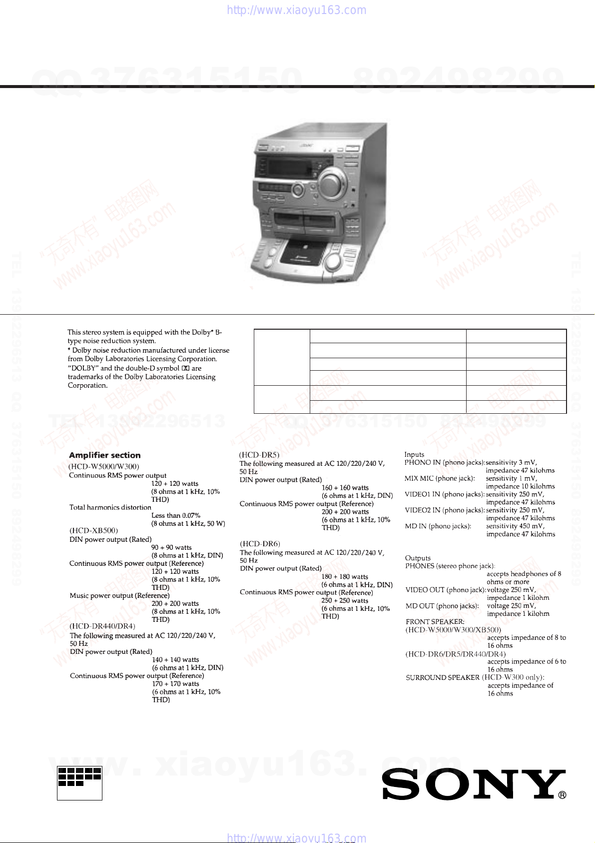
Photo: HCD-DR6
CD
SECTION
TAPE DECK
SECTION
Model Name Using Similar Mechanism HCD-D290/G3300/XB3
CD Mechanism Type CDM37M-5BD32L
Base Unit Type BU-5BD32L
Optical Pick-up Type KSS-213D/Q-N
Model Name Using Similar Mechanism NEW
T ape Transport Mechanism T ype TCM-230AWR2/230PWR2
8
9
2
4
9
Canadian Model
HCD-DR4/DR5/DR6/DR440
Australian Model
2
8
AEP Model
9
US Model
HCD-W300/W5000
HCD-W300
UK Model
HCD-XB500
E Model
9
TEL 13942296513 QQ 376315150 892498299
HCD-DR4
TEL
13942296513
6
7
3
Q
Q
SPECIFICATIONS
3
1
5
1
5
0
9
2
8
9
4
2
9
8
— Continued on next page —
9
w
w
MICROFILM
w
.
xia
COMPACT DISC DECK RECEIVER
o
y
u
1
6
3
– 1 –
.
c
o
m
7
Q
Q
TEL 13942296513 QQ 376315150 892498299
3
6
3
1
5
1
5
0
8
9
2
4
9
8
2
9
9
TEL 13942296513 QQ 376315150 892498299
TEL
13942296513
Q
Q
3
7
6
3
1
5
1
5
0
8
9
2
4
9
8
2
9
9
w
w
w
.
xia
o
y
u
1
6
3
– 2 –
.
c
o
m
0.15µF
To Exposed Metal
Parts on Set
1.5k
Ω
AC
voltmeter
(0.75V)
Earth Ground
CAUTION
Q
TEL 13942296513 QQ 376315150 892498299
Use of controls or adjustments or performance of procedures
Q
other than those specified herein may result in hazardous radiation exposure.
Notes on chip component replacement
• Never reuse a disconnected chip component.
• Notice that the minus side of a tantalum capacitor may be
damaged by heat.
Flexible Circuit Board Repairing
• Keep the temperature of soldering iron around 270˚C
during repairing.
• Do not touch the soldering iron on the same conductor of the
circuit board (within 3 times).
• Be careful not to apply force on the conductor when soldering
or unsoldering.
Laser component in this product is capable of emitting radiation
exceeding the limit for Class 1.
3
7
6
3
1
5
1
5
This appliance is classified as
a CLASS 1 LASER product.
The CLASS 1 LASER PRODUCT MARKING is located on
the rear exterior.
0
After correcting the original service problem, perform the following safety checks before releasing the set to the customer:
Check the antenna terminals, metal trim, “metallized” knobs, screws,
and all other exposed metal parts for AC leakage. Check leakage as
described below.
LEAKAGE
The AC leakage from any exposed metal part to earth Ground and
from all exposed metal parts to any exposed metal part having a
return to chassis, must not exceed 0.5 mA (500 microampers). Leakage current can be measured by any one of three methods.
1. A commercial leakage tester, such as the Simpson 229 or RCA
WT-540A. Follow the manufacturers’ instructions to use these
instruments.
2. A battery-operated AC milliammeter. The Data Precision 245
digital multimeter is suitable for this job.
3. Measuring the voltage drop across a resistor by means of a V OM
or battery-operated A C v oltmeter. The “limit” indication is 0.75
V, so analog meters must have an accurate low-voltage scale.
The Simpson 250 and Sanwa SH-63Trd are examples of a passive VOM that is suitable. Nearly all battery operated digital
multimeters that have a 2V AC range are suitable. (See Fig. A)
8
SAFETY CHECK-OUT
4
2
9
9
8
2
9
9
TEL 13942296513 QQ 376315150 892498299
TEL
13942296513
This caution
label is located
inside the unit.
Q
Q
2
8
9
4
2
9
8
0
5
1
5
1
3
6
7
3
Fig. A. Using an AC voltmeter to check AC leakage.
9
9
w
COMPONENTS IDENTIFIED BY MARK ! OR DO TTED LINE
WITH MARK ! ON THE SCHEMATIC DIAGRAMS AND IN
THE PARTS LIST ARE CRITICAL TO SAFE OPERATION.
REPLACE THESE COMPONENTS WITH SONY PARTS
WHOSE PART NUMBERS APPEAR AS SHOWN IN THIS
w
MANUAL OR IN SUPPLEMENTS PUBLISHED BY SONY.
SAFETY-RELATED COMPONENT WARNING !!
w
.
xia
o
y
u
1
ATTENTION AU COMPOSANT AYANT RAPPORT
À LA SÉCURITÉ!!
LES COMPOSANTS IDENTIFIÉS P AR UNE MARQUE ! SUR
LES DIAGRAMMES SCHÉMATIQUES ET LA LISTE DES
PIÈCES SONT CRITIQUES POUR LA SÉCURITÉ DE
FONCTIONNEMENT . NE REMPLACER CES COMPOSANTS
QUE PAR DES PIÈCES SONY DONT LES NUMÉROS
6
3
.
c
o
m
SONT DONNÉS DANS CE MANUEL OU DANS LES
SUPPLÉMENTS PUBLIÉS PAR SONY.
– 3 –
MODEL IDENTIFICATION
— BACK PANEL —
Q
Q
TEL 13942296513 QQ 376315150 892498299
3
7
Parts No.
6
3
1
5
1
5
0
MODEL PRODUCT COUNTRY PARTS No.
DR4: E, AR model INDONESIA PRODUCT 4-214-786-0π
DR4: TH model THAI PRODUCT 4-214-786-9π
DR4: SP model INDONESIA PRODUCT 4-214-786-1π
DR4: MX model INDONESIA PRODUCT 4-214-786-2π
DR4: AUS model INDONESIA PRODUCT 4-214-786-3π
DR4: EA model INDONESIA PRODUCT 4-214-786-4π
DR5: E, AR model INDONESIA PRODUCT 4-214-786-5π
DR5: SP model INDONESIA PRODUCT 4-214-786-6π
DR5: MX model INDONESIA PRODUCT 4-214-786-7π
DR440: MX model INDONESIA PRODUCT 4-214-786-8π
W300: US model INDONESIA PRODUCT 4-214-787-4π
W300: CND model INDONESIA PRODUCT 4-214-787-5π
W5000: US model INDONESIA PRODUCT 4-214-787-6π
DR6: E, AR model INDONESIA PRODUCT 4-214-788-3π
DR6: MX model INDONESIA PRODUCT 4-214-788-5π
XB500: AEP, UK model INDONESIA PRODUCT 4-214-785-0π
XB500: AEP model THAI PRODUCT 4-214-785-2π
8
9
2
4
9
8
2
9
9
TEL 13942296513 QQ 376315150 892498299
• Abbreviation
CND : Canadian model
TH : Thailand model
SP : Singapore model
MX : Mexican model
AUS : Australian model
EA : Saudi Arabia model
AR : Argentine model
TEL
NOTES ON HANDLING THE OPTICAL PICK-UP BLOCK
OR BASE UNIT
The laser diode in the optical pick-up block may suffer electrostatic
break-down because of the potential difference generated by the
charged electrostatic load, etc. on clothing and the human body.
During repair, pay attention to electrostatic break-down and also
use the procedure in the printed matter which is included in the
repair parts.
The flexible board is easily damaged and should be handled with
care.
NOTES ON LASER DIODE EMISSION CHECK
The laser beam on this model is concentrated so as to be focused on
the disc reflective surface by the objective lens in the optical pickup block. Therefore, when checking the laser diode emission, observe from more than 30 cm away from the objective lens.
13942296513
8
9
4
2
9
8
0
5
1
5
1
3
6
7
3
Q
Q
SECTION 1
SERVICING NOTE
About CD-TEXT display
This unit is provided with a simple CD-TEXT display function.
The CD-TEXT contents of 20 tracks are displayed on the fluorescent display tube.
Since the function is simple, some special characters may not be
displayed, or may be displayed as other characters.
2
9
9
LASER DIODE AND FOCUS SEARCH OPERATION
CHECK
Carry out the “S curve check” in “CD section adjustment” and check
that the S curve waveform is output four times.
w
w
w
.
xia
o
y
u
– 4 –
1
6
3
.
c
o
m

TABLE OF CONTENTS
7
Q
Q
TEL 13942296513 QQ 376315150 892498299
TEL
3
1. SERVICING NOTE .......................................................... 4
2. GENERAL ....................................................................6
2. DISASSEMBLY
3-1. Front Panel ............................................................................ 8
3-2. Main Board ........................................................................... 8
3-3. Sub Panel .............................................................................. 9
3-4. CD-L/CD-R Board and CD LID Assembly .......................... 9
3-5. Tape Mechanism Deck and Cassette LID...........................10
3-6. CD Mechanism Deck .......................................................... 10
3-7. Base Unit.............................................................................10
3-8. Disc Table ........................................................................... 11
4. SERVICE MODE ............................................................ 12
5. MECHANICAL ADJUSTMENTS ..........................16
6. ELECTRICAL ADJUSTMENTS ...............................16
7. DIAGRAMS
7-1. Circuit Boards Location ...................................................... 20
7-2. Block Diagrams
• BD (CD) Section.............................................................. 21
• Deck Section .................................................................... 23
• Main (1/2) Section ........................................................... 25
• Main (2/2) Section ........................................................... 27
• Power Section (DR4, DR5, DR6, DR440 model) ........... 29
• Power Section (W300, W5000, XB500 model)............... 31
13942296513
• Display Section ................................................................ 33
7-3. Printed Wiring Board – BD (CD) Section – ....................... 37
7-4. Schematic Diagram – BD (CD) Section – .......................... 39
7-5. Printed Wiring Board – Main Section – .............................. 41
7-6. Schematic Diagram – Main (1/5) Section – ........................ 43
7-7. Schematic Diagram – Main (2/5) Section – ........................ 45
7-8. Schematic Diagram – Main (3/5) Section – ........................ 47
7-9. Schematic Diagram – Main (4/5) Section – ........................ 49
7-10. Schematic Diagram – Main (5/5) Section – ..................... 51
7-11. Schematic Diagram – Deck Section – .............................. 53
7-12. Printed Wiring Board – Deck Section – ........................... 55
7-13. Schematic Diagram – Power (1/2) Section –
(DR4, DR5, DR6, DR440 model) .................................... 57
7-14. Schematic Diagram – Power (2/2) Section –
(DR4, DR5, DR6, DR440 model) .................................... 59
7-15. Printed Wiring Board – Power Section –
(DR4, DR5, DR6, DR440 model) .................................... 61
6
3
1
5
1
5
0
Q
Q
7-16. Schematic Diagram – Power (1/2) Section –
7-17. Schematic Diagram – Power (2/2) Section –
7-18. Printed Wiring Board – Power Section –
7-19. Schematic Diagram – Panel FL Section – ........................ 69
7-20. Printed Wiring Board – Panel FL Section – ..................... 71
7-21. Schematic Diagram – Panel VR Section – ....................... 73
7-22. Printed Wiring Board – Panel VR Section – .................... 75
7-23. Schematic Diagram – TC Panel Section – ....................... 77
7-24. Printed Wiring Board – TC Panel Section –..................... 79
7-25. Schematic Diagram – CD Panel Section – ....................... 81
7-26. Printed Wiring Board – CD Panel Section – .................... 83
7-27. Schematic Diagram – CD Motor Section – ...................... 85
7-28. Printed Wiring Board – CD Motor Section –...................87
7-29. Schematic Diagram – Jack Section – ............................... 89
7-30. Printed Wiring Board – Jack Section – ............................ 91
7-31. Schematic Diagram – Trans Section –
7-32. Printed Wiring Board – Trans Section –
7-33. Schematic Diagram – Trans Section –
7-34. Printed Wiring Board – Trans Section –
7-35. Schematic Diagram – Leaf SW Section – ...................... 100
7-36. Printed Wiring Board – Leaf SW Section – ................... 100
7-37. IC Block Diagrams ......................................................... 101
7-38. IC Pin Functions ............................................................. 102
7
3
8. EXPLODED VIEWS
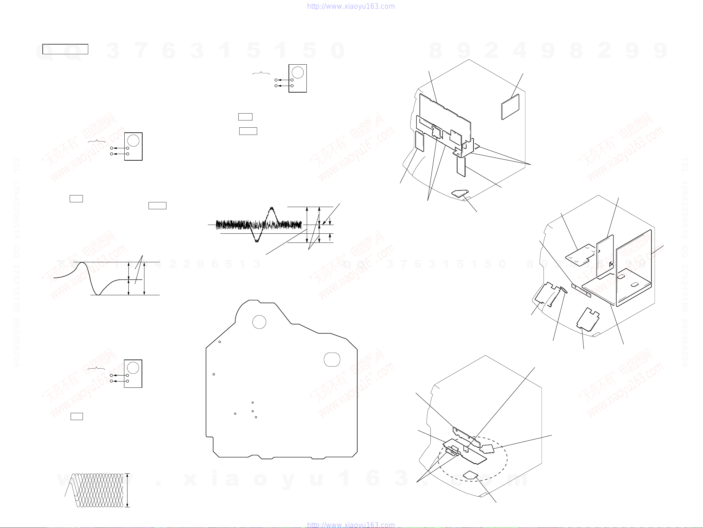
8-1. Case and Back Panel Section ............................................ 105
8-2. Front Panel Section 1 ........................................................ 106
8-3. Front Panel Section 2 ........................................................ 107
8-4. Chassis Section ................................................................. 108
8-5. TC Mechanism Section 1 (TCM230AWR2/230PWR2)... 109
8-6. TC Mechanism Section 2 (TCM230AWR2/230PWR2)... 110
8-7. CD Mechanism Section (CDM37M-5BD32L).................111
8-8. Base Unit Section (BU-5BD32L) ..................................... 112
9. ELECTRICAL PARTS LIST ...................................... 113
4
2
9
8
(W300, W5000, XB500 model) ....................................... 63
(W300, W5000, XB500 model) ....................................... 65
(W300, W5000, XB500 model) ....................................... 67
(W300, W5000, XB500 model) ....................................... 93
(W300, W5000, XB500 model) ....................................... 95
(DR4, DR5, DR6, DR440 model) .................................... 97
(DR4, DR5, DR6, DR440 model) .................................... 99
0
5
1
5
1
3
6
9
8
9
2
8
4
2
9
8
9
2
9
9
9
TEL 13942296513 QQ 376315150 892498299
w
w
w
.
xia
o
y
u
1
6
3
– 5 –
.
c
o
m
Front Panel
Q
Q
3
7
6
3
1
SECTION 2
GENERAL
5
1
5
0
10
8
11 12
9
2
4
9
8
2
9
9
2341
70
69
68
TEL 13942296513 QQ 376315150 892498299
67
66
63
65
64
606162
58
59
57
56
55
53
54
TEL
13942296513
56
79
8
Q
Q
3
7
13 14 15 16 17
5
1
5
1
3
6
0
26
28
27
8
29
18
19
20
21
22
9
23
2425
30
2
31 32
9
4
33
8
34
2
9
TEL 13942296513 QQ 376315150 892498299
9
52
51
50
49
48
47
35
37
36
39
40
41
42
43
44
4546
38
w
w
w
.
xia
o
y
u
1
6
3
– 6 –
.
c
o
m
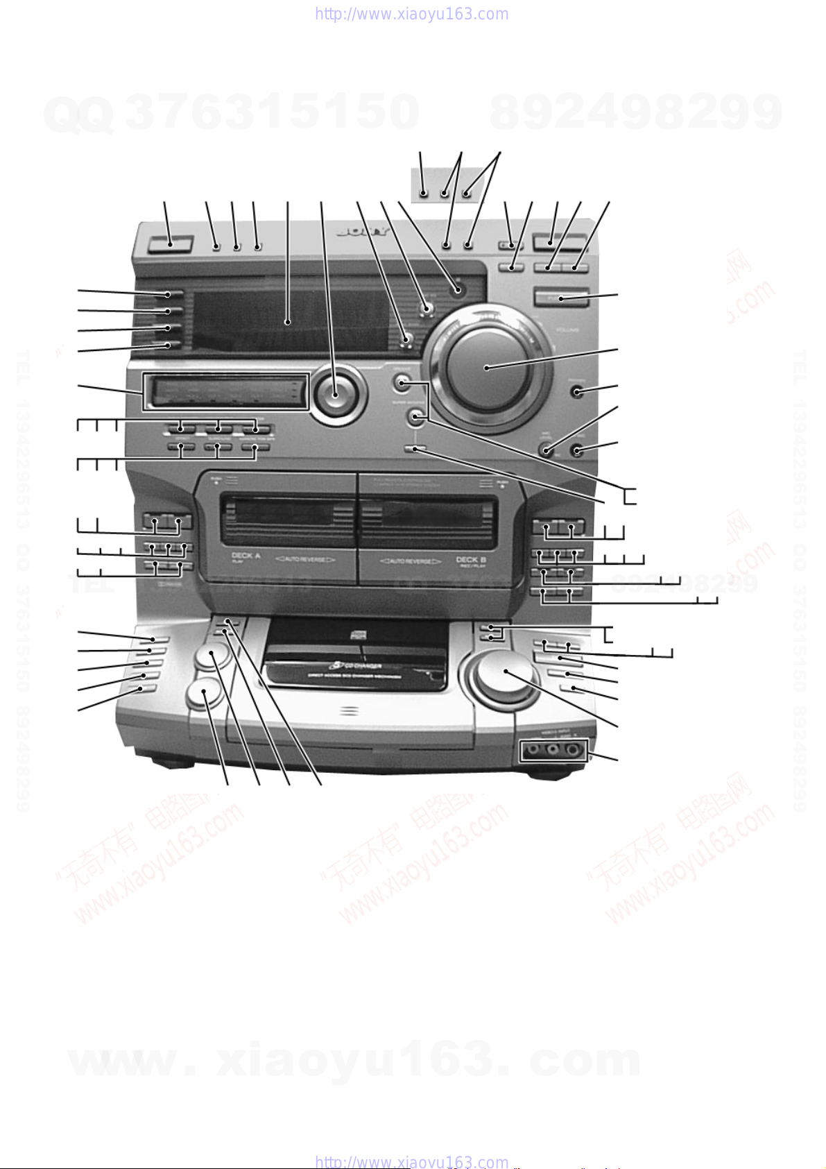
LOCATION OF PARTS AND CONTROLS
7
Q
Q
TEL 13942296513 QQ 376315150 892498299
3
1 1/u (Power) button and indicator
2 DEMO (STANDBY) button
(DR4/DR5/DR6/DR440)
POWER SAVE/DEMO (STANDBY)
button (W300/W5000/XB500)
3 DISPLAY button
4 SPECTRUM ANALYZER button
5 Display window
6 GEQ control button
7 SYNC BASS button
8 SYNC EQ button
9 Remote sensor
10 PTY button (XB500)
11 TUNING MODE button
12 STEREO/MONO button
13 ENTER/NEXT button and indicator
14 TUNER MEMORY button
15 TUNER/BAND button
16 TUNING - button
17 TUNING + button
18 FUNCTION button
19 VOLUME knob
20 PHONES jack
21 MIC LEVEL knob
22 MIX MIC jack
23 GROOVE button and indicator
6
3
1
5
1
5
24 SUPER WOOFER button and indicator
25 MODE button
26 ª (B Deck) button and indicator
27 · (B Deck) button and indicator
28 p (B Deck) button
29 0 (B Deck) button
30 ) (B Deck) button
31 P (B Deck) button
32 r REC (B Deck) button
33 HI-SPEED DUB button
34 CD SYNCHRO button
35 PLAY MODE button
36 REPEAT button
37 0 (CD) button
38 ) (CD) button
39 ·P (CD) button and indicator
40 p (CD) button
41 DISK SKIP button
42 = AMS + knob
43 VIDEO2 INPUT jacks
44 EDIT button
45 NON-STOP button and indicator
46 LOOP button
47 FLASH button
48 DISC 5 button
49 DISC 4 button
0
8
9
4
2
50 DISC 3 button
51 DISC 2 button
52 DISC 1 button
53 DOLBY NR button
54 DIRECTION button
55 ) (A Deck) button
56 0 (A Deck) button
57 p (A Deck) button
58 · (A Deck) button
59 ª (A Deck) button
60 KARAOKE PON/MPX button
61 SURROUND button and indicator
62 EFFECT button and indicator
63 ENTER button and indicator
64 GEQ CONTROL button
65 P. FILE MEMORY
66 Equalizer indicators
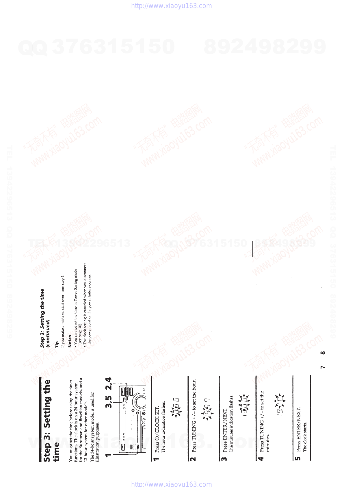
67 t/CLOCK SET button
68 SLEEP button
69 REC button and indicator
70 DAILY button and indicator
• AMS is the abbreviation for Automatic
Music Sensor.
9
8
2
9
9
TEL 13942296513 QQ 376315150 892498299
TEL
13942296513
Q
Q
3
7
6
3
1
5
1
5
9
4
2
9
8
0
This section is extracted from
instruction manual.
8
2
9
9
w
w
w
.
xia
o
y
u
1
6
3
– 7 –
.
c
o
m
)
SECTION 3
DISASSEMBLY
Note: Follow the disassembly procedure in the numerical order given.
Q
Q
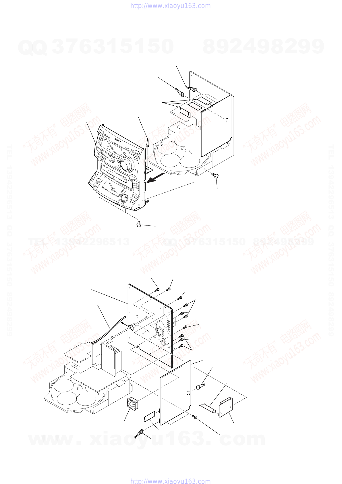
3-1. FRONT PANEL
3
7
7
6
Front panel
1
3
4
5
2
Connector (CN702)
1
Three flat type wires
(CN303,CN304,CN431)
Connector (CN802)
1
3
Connector (CN452)
5
0
8
9
2
4
9
8
2
9
9
TEL 13942296513 QQ 376315150 892498299
6
Four screw (BVTP 3x8)
TEL
3-2. MAIN BOARD
13942296513
!£
Screw (BVTP 3x8)
(HCD-W300/W5000/XB500)
!∞
Back panel
!¢
Power cord
3
Q
Q
!™
Screw (BVTP 3x8)
(HCD-XB500)
2
7
Two screws (BVTP 3x8)
0
(HCD-DR4/DR440/W300/W5000)
9
Three screws (BVTP 3x8)
5
Screw (BVTP 3x8
0
5
1
5
1
3
6
Two screws (BVTP 3x8)
8
9
2
4
9
8
2
9
TEL 13942296513 QQ 376315150 892498299
9
w
w
w
.
xia
!¡
Fan motor
(Except XB500)
o
0
Two screws (BVTP 3x8)
(HCD-DR5/DR6)
8
Two screws (BVTP 3x8)
7
Seven screws (BVTP 3x8)
!¶
5
Flat type wire (CN411)
4
y
Connector (CN412)
u
1
6
– 8 –
3
.
Main board
6
Connector (CN903)
(Except XB500)
1
Flat type wire (CN1)
3
T uner unit
!§
Two screws (BVTP 3x8)
c
o
m
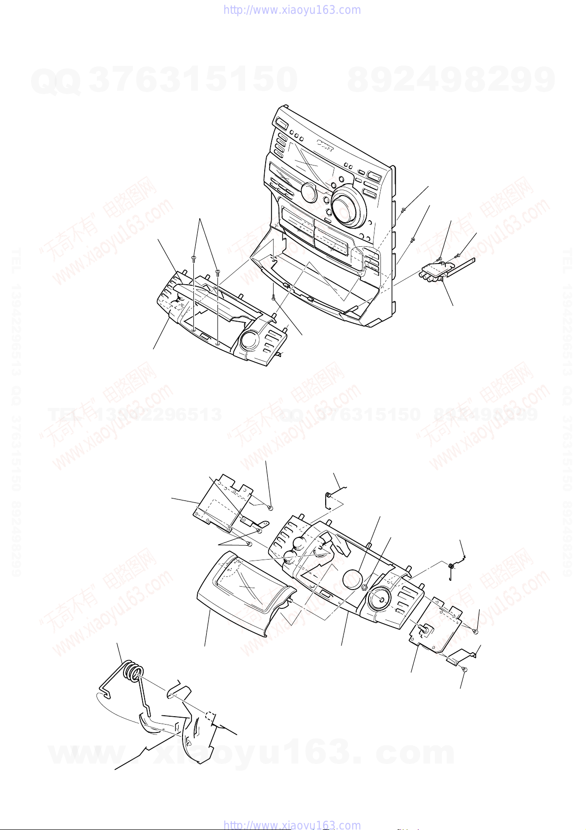
3-3. SUB PANEL
7
Q
Q
TEL 13942296513 QQ 376315150 892498299
3
4
Open the CD lid assembly
6
5
Two screws (BTP 2.6x6)
3
1
5
1
5
0
8
9
2
4
9
8
Three screws (BVTP 2.6x8)
7
Two screws (BVTP 2.6x8)
1
Two screws (BVTP 2.6x8)
2
8
2
Screw (BVTP 3x8)
9
9
TEL 13942296513 QQ 376315150 892498299
9
Sub panel block
TEL
13942296513
3-4. CD-L/CD-R BOARD AND CD LID ASSEMBLY
1
Three screws (BVTP 2.6x8)
3
Bracket (CD-L)
4
CD-L board
2
Three screws
(BVTP 2.6x8)
Q
6
Screw (BVTP 3x8)
7
3
Q
!™
5
1
5
1
3
6
Torsion spring (CD-L)
5
Knob (CD)
6
Nut
0
3
Front input board
2
9
8
!¡
9
9
2
8
9
4
Torsion spring (CD-R)
Torsion spring (CD-L)
Sub panel assembly
w
w
w
.
xia
!£
CD lid assembly
CD lid assembly
o
y
u
Sub panel assembly
1
6
– 9 –
3
.
0
CD-R board
c
o
7
Three screws
(BVTP 2.6x8)
9
Bracket (CD-R)
8
Two screws (BVTP 2.6x8)
m
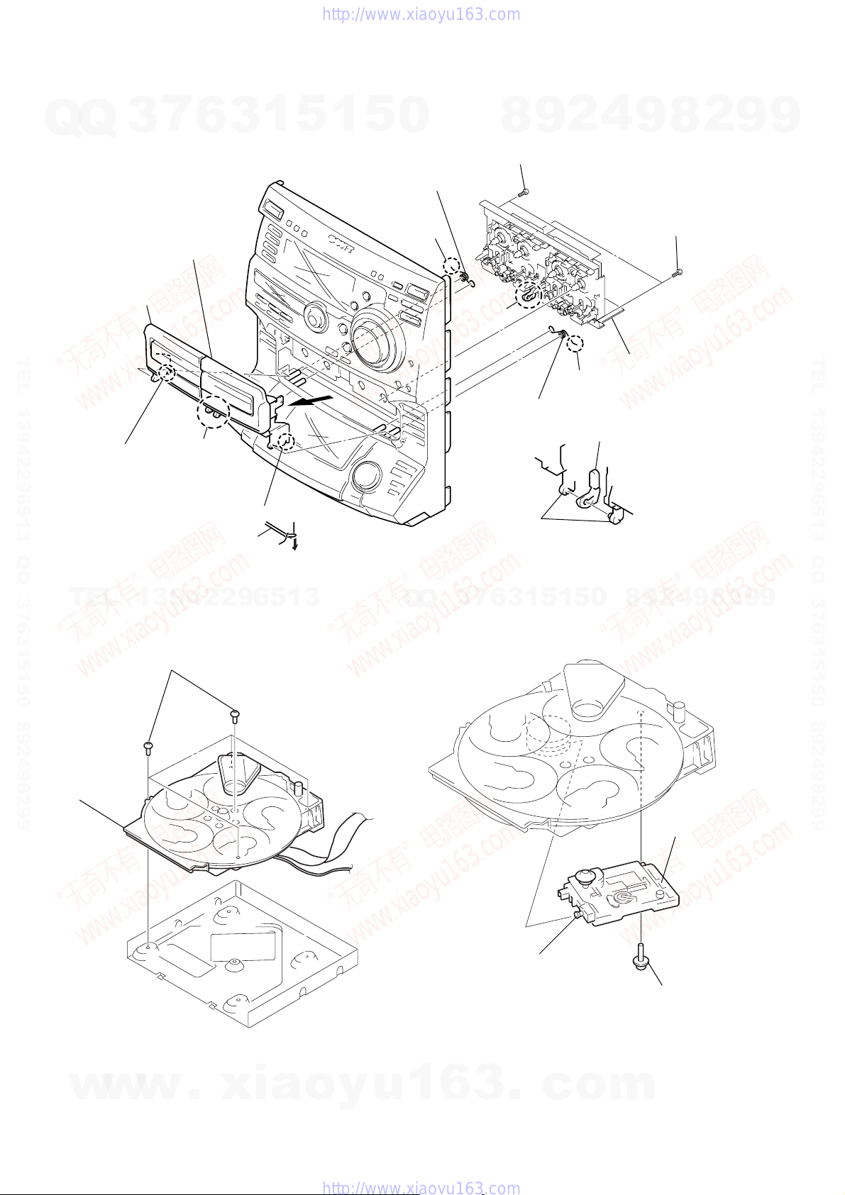
t
3-5. TAPE MECHANISM DECK AND CASSETTE LID
Q
Q
6
Cassette lid (A) block
7
3
5
Cassette lid (B) block
6
3
1
5
1
5
0
4
Torsion spring (TC-A)
Portion
A
9
8
7
Two screws (BVTP 2.6x8)
Portion
C
2
4
8
9
8
Three screws
(BVTP 2.6x8)
2
9
9
TEL 13942296513 QQ 376315150 892498299
Portion
2
Release
(Refer to order No.
TEL
3-6. CD MECHANISM DECK 3-7. BASE UNIT
13942296513
B
1
)
1
Portion
A
1
Five screws (BVTP3x8)
Release
Q
Q
3
7
Portion
3
6
Portion
A
3
Torsion spring (TC-B)
Portion
B
0
5
1
5
1
9
T ape mechanism
C
4
2
9
8
9
8
2
9
TEL 13942296513 QQ 376315150 892498299
9
2
CD mechanism
deck
w
w
w
.
xia
o
y
u
1
– 10 –
6
3
.
2
Boss
c
o
m
3
Base uni
1
Yoke fitting
Q
3-8. DISC TABLE
7
Q
3
Note:
When the disc table is installed, adjust the positions of
roller cam and mark ” as shown in the figure, then set to
the groove of disc table.
6
3
A
1
5
1
5
0
2
Screw (BVTP3X8)
3
Bracket (BU)
2
9
8
1
Screw (BVTP3X8)
4
9
4
2
8
Stop screw
5
Disc table
9
9
TEL 13942296513 QQ 376315150 892498299
TEL
13942296513
Q
Q
3
7
6
3
1
5
1
5
A
0
8
9
2
4
9
8
2
9
TEL 13942296513 QQ 376315150 892498299
9
w
w
w
.
xia
o
y
u
1
6
3
– 11 –
.
c
o
m
SECTION 4
SERVICE MODE
MC Cold Reset
• The cold reset clears all data including preset data stored in the RAM to initial conditions. Execute this mode when returning the set to the
Q
Q
customer.
Procedure:
1. Press three buttons t/CLOCK SET , ENTER , and 1/u simultaneously.
2. “COLD RESET” is displayed on the fluorescent display tube and reset is executed.
CD Delivery Mode
• This mode moves the pick-up to the position durable to vibration. Use this mode when returning the set to the customer after repair.
Procedure:
1. Press 1/u button to turn the set ON.
2. Press LOOP button and 1/u button simultaneously.
3. A message “LOCK” is displayed on the fluorescent indicator tube, and the CD delivery mode is set.
MC Hot Reset
• This mode resets the set with the preset data kept stored in the memory . The hot reset mode functions same as if the po wer cord is plugged
in and out.
TEL 13942296513 QQ 376315150 892498299
Procedure:
1. Press three buttons t/CLOCK SET , ENTER , and DISC 1 simultaneously.
2. The fluorescent indicator tube becomes blank instantaneously, and the set is reset.
3
7
6
3
1
5
1
5
0
8
9
2
4
9
8
2
9
9
TEL 13942296513 QQ 376315150 892498299
Sled Servo Mode
• This mode can run the CD sled motor freely. Use this mode, for instance, when cleaning the pick-up.
Procedure:
1. Press 1/u button to turn the set ON.
2. Press three buttons t/CLOCK SET , ENTER , and DISC 5 simultaneously.
3. The Sled Servo mode is selected, if “CD” is blanking on the fluorescent indicator tube.
4. With the CD in stop status, When the = AMS + knob is rotated in the clockwise direction, the pick-up moves outside. When
rotated counterclockwise, it moves inside.
5. To exit from this mode, perform as follows:
1) Move the pick-up to the most inside track.
2) Execute MC cold reset. (Press the three buttons t/CLOCK SET , ENTER , and 1/u button simultaneously.)
Note:
TEL
• Always move the pick-up to most inside track when exiting from this mode. Otherwise, a disc will not be unloaded.
• Do not run the sled motor excessively, otherwise the gear can be chipped.
Change-over of AM Tuner Step between 9kHz and 10kHz
• A step of AM channels can be changed over between 9kHz and 10kHz.
Procedure:
1. Press 1/u button to turn the set ON.
2. Select the function “TUNER”, and press TUNER/BAND button to select the BAND “AM”.
3. Press 1/u button to turn the set OFF.
4. Press ENTER and 1/u buttons simultaneously, and the display of fluorescent indicator tube changes to “AM 9k STEP” or “AM 10k
STEP”, and thus the channel step is changed over.
LED and Fluorescent Indicator Tube All Lit, Key Check Mode
Procedure:
1. Press three buttons t/CLOCK SET , ENTER , and DISC 2 simultaneously.
2. LEDs and fluorescent indicator tube are all turned on.
Press DISC 2 button, and the key check mode is activated.
3. In the key check mode, the fluorescent indicator tube displays “K @ V0 J0”. Each time a button is pressed , “K”value increases. Howe ver ,
once a button is pressed, it is no longer taken into account.
“J” Value increases like 1, 2, 3 ... if rotating = AMS + knob in “+” direction, or it decreases like 0, 9, 8 ... if rotating in “-”
direction.
“V” Value increases like 1, 2, 3 ... if rotating VOLUME knob in “+” direction, or it decreases like 0, 9, 8 ... if rotating in “-” direction.
4. To exit from this mode, press three buttons in the same manner as step 1, or disconnect the power cord.
13942296513
Q
Q
3
7
6
3
1
5
1
5
0
8
9
2
4
9
8
2
9
9
w
w
w
.
xia
o
y
u
1
6
3
– 12 –
.
c
o
m
AMS Test Mode
Q
TEL 13942296513 QQ 376315150 892498299
• This mode is used for checking the AMS operations of the tape deck.
Q
JIG
7-819-039-12 Alignment tape, AMS-110A
Procedure:
1. Press the 1/u button to turn the set ON.
2. Set the tape (AMS-110A).
3. Press the three buttons t/CLOCK SET , ENTER , and DISC 3 button simultaneously.
4. “TEST MODE” is displayed on the fluorescent display tube.
5. Press the FUNCTION button and switch the function to the deck with the tape (AMS-110A).
6. Press the CD SYNCHRO button. “AMS CHECK” is displayed on the fluorescent display tube and the tape is rewound.
7. AMS starts in the normal direction. If the AMS count is 2 at shut down, proceed to step 8.
“NG” is displayed at other times, and the deck stops.
8. AMS starts in the opposite direction. If the AMS count is 2 at shut down again, “OK” is displayed.
“NG” is displayed at other times.
Aging Mode
During the aging mode, both the CD player and tape deck are executed together.
• If an error occurs:
Aging stops, and the error state is displayed on the fluorescent display tube.
• If no error occurs:
Aging is repeated.
3
7
6
3
1
5
1
5
0
8
9
2
4
9
8
2
9
9
TEL 13942296513 QQ 376315150 892498299
Procedure:
1. Press the 1/u button to turn the set ON.
2. Load 10 minute tapes with unbent rec-proof tabs in decks A and B.
3. Set CDs on the DISC 1 and DISC 4 tables.
4. Set the CD mode REPEAT to OFF and PLAY MODE to ALL DISCS.
(Press the PLAY MODE and REPEAT buttons to set these modes.)
5. Press the FUNCTION button to switch the function to “CD”.
6. Press the three buttons t/CLOCK SET , ENTER , and DISC 4 button simultaneously.
TEL
13942296513
7. Aging starts.
8. To end aging, press the 1/u button to turn the set OFF.
Aging Sequence:
Aging is performed in the following sequence.
• T a pe Deck
1. The tape in deck A is rewound. “TAPE A AG-1” is displayed.
2. The FWD side of deck A is played for two minutes.
“TAPE A AG-2” is displayed.
3. The tape in deck A is fast forwarded. “TAPE A AG-3” is displayed. Fast forward is carried out for 20 seconds or to the tape end.
4. The RVS side of deck A is played for two minutes.
“TAPE A AG-4” is displayed.
5. The tape in deck A is rewound. “TAPE A AG-5” is displayed.
6. The FWD side of deck B is played for two minutes.
“TAPE B AG-2” is displayed.
7. The tape in deck B is fast forwarded. “TAPE B AG-3” is displayed. Fast forward is carried out for 20 seconds or to the tape end.
8. The RVS side of deck B is played for two minutes.
“TAPE B AG-4” is displayed.
9. The tape in deck A is rewound. “TAPE A AG-5” is displayed.
10. Repeated from step 2.
Q
Q
3
7
6
3
1
5
1
5
0
8
9
2
4
9
8
2
9
9
• CD
1. The tray rotates.
2. DISC 1 is chucked.
3. The TOC is read.
4. The first track is played for 2 seconds.
5. The last track is played for 2 seconds.
6. The tray rotates.
7. DISC 4 is chucked.
8. The TOC is read.
9. The first track is played for 2 seconds.
w
w
w
10. The last track is played for 2 seconds.
11. Repeated from step 1.
.
xia
o
y
u
1
6
3
– 13 –
.
c
o
m
• Display when ended abnormally
When the tape deck is abnormal:
Q
Q
The state when ended abnormally is displayed.
The contents of display are the same as that during aging.
When the CD player is abnormal:
A message indicating that errors such as “CD MEC ERR” have occurred.
Check the error contents in the following error history display mode.
Error History Display Mode
Mode which enables the history of error occurring in the CD player to be checked.
Execute this mode after ending the aging mode.
Procedure:
TEL 13942296513 QQ 376315150 892498299
1. Press the 1/u button to turn the set ON.
2. Press the three buttons t/CLOCK SET , ENTER , and CD SYNCHRO simultaneously.
3. A message such as “EMC@@EDC**” is displayed.
@@ : Number of mechanical errors (Up to three past errors)
** : Number of errors (NO DISC ERROR) which occurs after chucking (Up to three past errors)
4. When checking the history of mec hanical errors, press the PLAY MODE button. When checking errors after chucking, press the
REPEAT button to switch the display.
5. Press the 1/u button to end and turn the set OFF.
6. To erase the error history, perform COLD reset.
(Press the three buttons t/CLOCK SET , ENTER , and DISC 1 simultaneously.
3
7
6
3
1
5
1
5
0
8
9
2
4
9
8
2
9
9
TEL 13942296513 QQ 376315150 892498299
• Viewing the mechanical error history display
(Switch the history by pressing the PLAY MODE button.)
Display
E@@M#*****
TEL
@@ : Error number. 00 is the newest.
# : Operating state of table
0 : Currently in the INITIAL mode
7 : Currently rotating to the right
8 : Currently rotating to the left
A : Currently chucking down
B : Currently chucking up
* : In valid
13942296513
Q
Q
3
7
6
3
1
5
1
5
0
8
9
2
4
9
8
2
9
9
w
w
w
.
xia
o
y
u
1
6
3
– 14 –
.
c
o
m

• Viewing the NO DISC ERROR history display
Q
TEL 13942296513 QQ 376315150 892498299
(Switch the history by pressing the REPEAT button.)
Q
Display
E@@D##$$%*
@@ : Error number. 00 is the newest
## : Error contents
$$ : Retries
% : State when determined as NO DISC
1 : When stopped
2 : At setup
3 : At TOC READ
4 : When accessing
5 : When playing
6 : When pausing
7 : When manual searching (during play)
8 : When manual searching (during pausing)
* : In valid
7
3
01: Focus error
02: GFS error
03: Setup error
00: NO DISC is determined without attempting chucking retry
02: NO DISC is determined after chucking retry.
6
3
1
5
1
5
0
8
9
2
4
9
8
2
9
9
TEL 13942296513 QQ 376315150 892498299
TEL
13942296513
Q
Q
3
7
6
3
1
5
1
5
0
8
9
2
4
9
8
2
9
9
w
w
w
.
xia
o
y
u
1
6
3
– 15 –
.
c
o
m
SECTION 5
MECHANICAL ADJUSTMENTS
Precaution
1. Clean the following parts with a denatured alcohol-moistened
Q
Q
swab:
record/playback heads pinch rollers
erase head rubber belts
capstan idlers
2. Demagnetize the record/playback head with a head demagnetizer.
3. Do not use a magnetized screwdriver for the adjustments.
4. After the adjustments, apply suitable locking compound to the
parts adjusted.
5. The adjustments should be performed with the rated power supply voltage unless otherwise noted.
Torque Measurement
TEL 13942296513 QQ 376315150 892498299
Mode
FWD
FWD
back tension
REV
REV
back tension
FF/REW
FWD tension
REV tension
3
7
6
Torque meter
CQ-102C
CQ-102C
CQ-102RC
CQ-102RC
CQ-201B
CQ-403A
CQ-403R
1
3
Meter reading
31 to 71 g • cm
(0.43 – 0.98 oz • inch)
2 to 6 g • cm
(0.02 – 0.08 oz • inch)
31 to 71 g • cm
(0.43 – 0.98 oz • inch)
2 to 6 g • cm
(0.02 – 0.08 oz • inch)
71 to 143 g • cm
(0.98 – 1.99 oz • inch)
100 g or more
(3.53 oz or more)
100 g or more
(3.53 oz or more)
5
1
5
0
ELECTRICAL ADJUSTMENTS
DECK SECTION 0 dB=0.775V
1. Demagnetize the record/playback head with a head damagnetizer.
2. Do not use a magnetized screwdriver for the adjustments.
3. After the adjustments, apply suitable locking compound to the
parts adjusted.
4. The adjustments should be performed with the rated power supply voltage unless otherwise noted.
5. The adjustments should be performed in the order given in this
service manual. (As a general rule, playback circuit adjustment
should be completed before performing recording circuit adjustment.)
6. The adjustments should be performed for both L-CH and R-CH.
7. Switches and controls should be set as follows unless otherwise
specified.
P-4-A100
WS-48B
P-4-L300
Record/Playback Head Azimuth Adjustment
(Deck A, Deck B)
Note: Perform this adjustments for both decks.
Procedure:
1. Mode : Playback
SECTION 6
9
8
Signal
10 kHz, –10 dB
3 kHz, 0 dB
315 Hz, 0 dB
2
4
9
Used forTape
Azimuth Adjustment
Tape Speed Adjustment
Level Adjustment
8
2
9
9
TEL 13942296513 QQ 376315150 892498299
TEL
13942296513
test tape
P-4-A100
(10kHz, –10dB)
Q
Q
2. Turn the adjustment screw and check output peaks. If the peaks
do not match for L-CH and R-CH, turn the adjustment screw so
that outputs match within 1 dB of peak.
L-CH
peak
screw
position
3
7
R-CH
peak
6
3
output
level
1
5
set
within
1 dB
1
0
5
MD OUT
L-CH
peak
8
2
9
level meter
R-CH
peak
+
–
4
8
9
within 1dB
screw
position
2
9
9
w
w
w
.
xia
o
y
u
1
6
3
– 16 –
.
c
o
m
)
Q
3. Mode: Playback Tape Speed Adjustment (Deck A)
Q
3
7
test tape
P-4-A100
(10kHz, –10dB)
6
3
1
5
MD OUT
1
5
oscilloscope
0
4
2
9
8
Note: Set the test mode using the following method and begin tape
speed adjustment.
In the test mode, the speed will switch to double speed or
normal speed each time the HI-SPEED DUB button is pressed.
9
8
2
9
9
set
Waveform of oscilloscope
TEL 13942296513 QQ 376315150 892498299
in phase 45
4. After the adjustments, apply suitable locking compound to the
parts adjusted.
Adjustment Location: Playback Head (Deck A)
Remove the cassette lid.
TEL
13942296513
°
good
Record/Playback/Erase Head (Deck B)
135
90
°
°
wrong
180
°
Q
Q
Procedure:
With the power turned ON, press the t/CLOCK SET button,
ENTER button, and DISC 3 button simultaneously.
(The “VOLUME” on the fluorescent display tube will blink while
in the test mode.)
To exit the test mode, press the 1/u button.
1. Insert the WS-48B into deck B.
2. Press the · button of deck B.
3. Press the HI-SPEED DUB button and play the tape at double speed.
4. Adjust RV1001 of the LEAF SW board so that the reading of
the frequency counter becomes 6000 ± 180 Hz.
5. Press the HI-SPEED DUB button and play the tape at normal speed.
6. Adjust RV1002 of the LEAF SW board so that the reading of
the frequency counter becomes 3000 ± 90 Hz.
Adjustment Location: LEAF SW board
Sample Value of Wow and flutter
W.RMS (JIS) less than 0.3%
(test tape: WS-48B)
Playback Level Adjustment (Deck A, Deck B)
Procedure:
Mode: Playback
7
3
1
3
6
test tape
P-4-L300
(315Hz, 0dB)
5
1
5
0
8
9
2
4
8
9
level meter
2
9
TEL 13942296513 QQ 376315150 892498299
9
Reverse Foward
w
w
w
.
xia
o
y
u
1
set
MD OUT
Deck A is RV311 (L-CH) and RV411 (R-CH), deck B is RV301
(L-CH) and RV401 (R-CH)
so that adjustment within the following adjustment level.
Adjustment level:
CN301 playback level: 301.5 to 338.3 mV (–8.2 to –7.2 dB)
level difference between the channels: within ± 0.5 dB
Adjustment Location: AUDIO board
Adjustment Location
[LEAF SW BOARD]
RV1001(High Speed)
RV1002(Normal Speed
RV1002 RV1001
6
3
.
c
o
m
– 17 –
Record Bias Adjustment (Deck B)
7
Q
Q
Procedure:
INTRODUCTION
When set to the test mode performed in Tape Speed Adjustment, when the tape is rewound after recording, the “REC memory
mode” which rewinds only the recorded portion and playback is
set.
This “REC memory mode” is convenient for performing this adjustment. During recording, the input signal FUNCTION will automatically switch to VIDEO 1.
(After recording, press the 0 button without stopping will return to the position where recording was started.)
1. Press FUNCTION button to select VIDEO 1. (This step is not
necessary if the above test mode has already been set.)
TEL 13942296513 QQ 376315150 892498299
2. Insert a tape into deck B, press the r REC button, and then
press the · button to start recording.
3. Mode: Record
AF OSC
3
attenuator
6
VIDEO 1 (AUDIO) IN
1) 315 Hz
2) 10 kHz
600
Ω
1
3
} 50 mV (–23.8 dB)
set
5
blank tape
CS-123
1
5
Record Level Adjustment (Deck B)
0
Procedure:
INTRODUCTION
When set to the test mode performed in Tape Speed Adjustment, when the tape is rewound after recording, the “REC memory
mode” which rewinds only the recorded portion and playback is
set.
This “REC memory mode” is convenient for performing this
adjustment. During recording, the input signal FUNCTION will automatically switch to VIDEO 1.
(After recording, press the 0 button without stopping will return to the position where recording was started.)
1. Press FUNCTION button to select VIDEO 1. (This step is not
necessary if the above test mode has already been set.)
2. Insert a tape into deck B, press the r REC button, and then
press the · button to start recording.
3. Mode: Record
AF OSC
attenuator
2
9
8
VIDEO 1 (AUDIO) IN
315Hz 50 mV (–23.8 dB)
600
Ω
4
set
9
2
8
blank tape
CS-123
9
9
TEL 13942296513 QQ 376315150 892498299
4. Mode: Playback
TEL
recorded
position
5. Confirm playback the signal recorded in step 2 become adjustment level as follows.
If these levels do not adjustment lev el, adjust the R V341 (L-CH)
and R V441 (R-CH) on the A UDIO board to repeat steps 3 and 4.
Adjustment level: The playback output of 10 kHz le vel dif ference
Adjustment Location: AUDIO board
Adjustment Location:
[AUDIO BOARD] (Conductor Side)
13942296513
set
MD OUT
against 315 Hz reference should be ± 1.0 dB.
RV341(Lch),RV441(Rch)
Record Bias
level meter
RV311(Lch),RV411(Rch)
Playback Level (Deck A)
4. Mode: Playback
8
9
4
2
9
8
0
5
1
5
1
3
6
7
3
Q
Q
5. Confirm playback the signal recorded in step 2 become adjust-
Adjustment level:
CN403 playback level: 47.2 to 53.0 mV (–24.3 to –23.3 dB)
Adjustment Location: MAIN board
recorded
position
set
MD OUT
ment level as follows.
If these levels do not adjustment lev el, adjust the R V301 (L-CH)
and R V351 (R-CH) on the MAIN board to repeat steps 3 and 4.
[MAIN BOARD] (Conductor Side)
level meter
2
9
9
RV301 RV401
w
RV441 RV341
RV301(Lch),RV401(Rch)
Playback Level (Deck B)
w
w
.
xia
RV411
RV311
o
y
u
1
– 18 –
1
3
IC301
6
3
RV351
Record Level (Rch)
Record Level (Lch)
RV301
14
15
28
1
29
56
42
43
.
c
o
m
TRANS board
SUB TRANS board
(W300/W5000/XB500)
MAIN board
PA board
CD-L board
CD-R board
LED (PANEL) board
DOOR SWITCH board
HCD-DR4/DR5/DR6/DR440/W300/W5000/XB500
SECTION 7
DIAGRAMS
CD SECTION
Q
Note:
1. CD Block is basically constructed to operate without adjustment.
2. Use YEDS-18 disc (3-702-101-01) unless otherwise indicated.
3. Use an oscilloscope with more than 10MΩ impedance.
4. Clean the object lens by an applicator with neutral detergent when
S Curve Check
TEL 13942296513 QQ 376315150 892498299
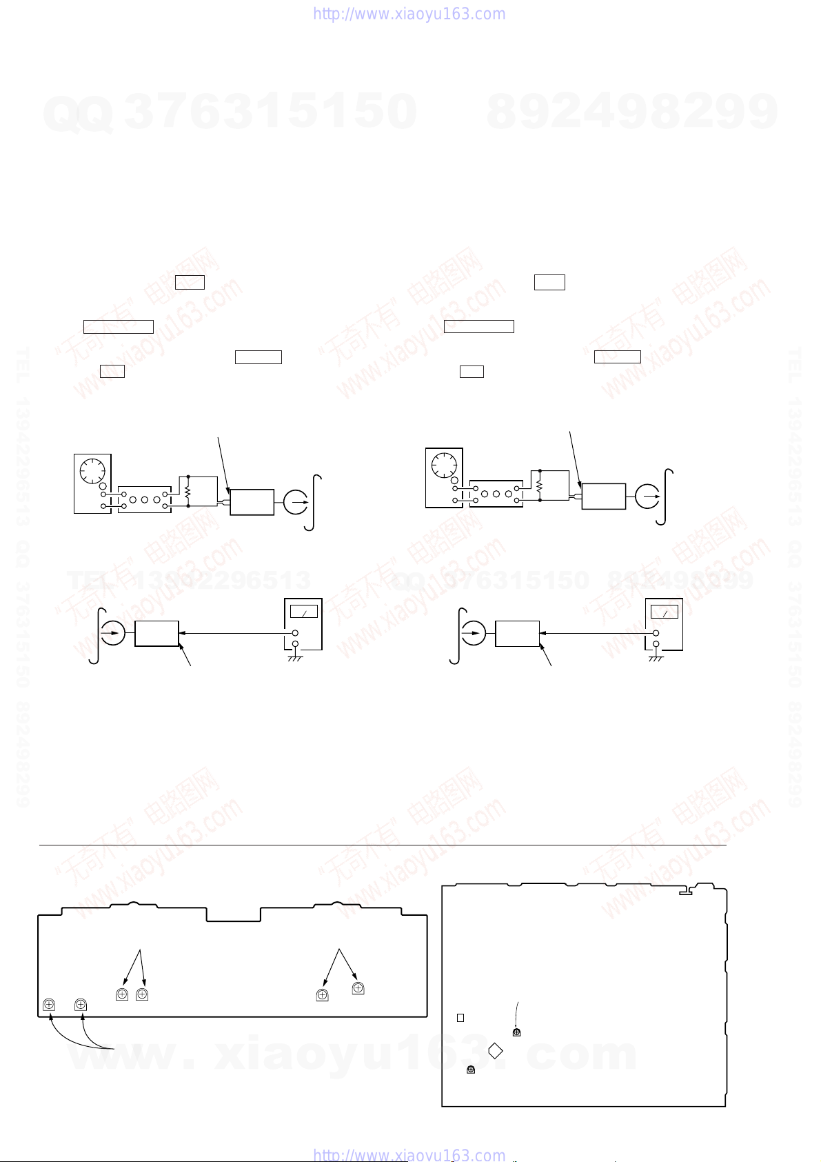
Procedure :
1. Connect the oscilloscope to test points TP (FE) and TP (VC).
2. Connect TP (FEI) and GND, and TP (AGCCON) and GND of
3. Press the 1/u button to turn the set ON.
4. With the disc (YEDS-18) loaded, press the ·P button and
5. Check the symmetry and peak to peak level of the oscilloscope
Q
Therefore, check each item in order given.
the signal level is low than specified value with the following
checks.
the BD board with lead wires.
perform focus search. (Focus search will be performed in the
same way even while the disc table is pushed in and out.)
waveform (S curve) at this time.
3
BD board
TP (FE)
TP (VC)
7
oscilloscope
+
–
6
E-F Balance (1 Track Jump) check
3
1
Procedure:
1. Connect oscilloscope to test point TP (TE) on BD board.
2. Press the 1 /u button to turn the unit ON.
3. Put disc (YEDS-18) in to play the number five track.
4. Press the ·P button.
5. Check the level B of the oscilloscope's waveform and
the A (DC voltage) of the center of the Traverse waveform.
Confirm the following:
• A/B x 100 = less then ± 22 (%)
• B = 1.3 ± 0.6 Vp-p
1 track jump waveform
0V
5
BD board
TP (TE)
TP (VC)
1
5
oscilloscope
+
–
0
Center of the waveform
B
A (DC voitage)
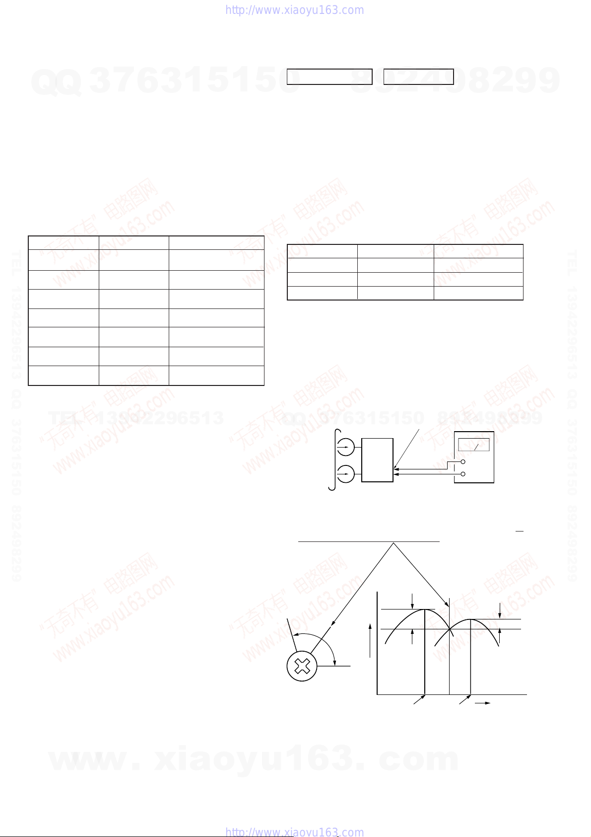
7-1. CIRCUIT BOARDS LOCATION
8
PANEL FL board
TC-A board
PANEL VR board
9
FRONT INPUT board
2
4
TUNER UNIT
TC-B board
9
JACK board
8
2
9
9
TEL 13942296513 QQ 376315150 892498299
S-curve waveform
T
E
L
6. After check, remove the lead wire connected in step 2.
Note: • Try to measure several times to make sure than the ratio of
A : B or B : A is more than 10 : 7.
• Tak e sweep time as long as possible and light up the brightness to obtain best waveform.
RF Level Check
BD board
TP (RF)
TP (VC)
Procedure :
1. Connect oscilloscope to test point TP (RF) and TP (VC) on BD
board.
2. Press the 1/u button to turn the set ON.
3. Put disc (YEDS-18) in and playback 5 track.
4. Confirm that oscilloscope waveform is clear and check RF signal level is correct or not.
Note: Clear RF signal waveform means that the shape “◊” can be
clearly distinguished at the center of the waveform.
1
symmetry
3
9
A
B
oscilloscope
+
–
4
Within 3
2
±
1 Vp-p
2
level : 1.3
9
6
5
1
3
Adjustment Location :
[ BD BOARD ] — SIDE A —
TP
(VC)
TP
(RF)
TP
(AGCCON)
TP
(TE)
TP
(FE1)
TP (FE)
±
0.6 Vp-p
Symmetry
Q
Q
7
3
LEAF SW board
AUDIO board
6
3
1
5
1
5
0
8
TABLE SENSOR board
9
4
2
BD board
9
8
2
9
9
RF signal waveform
w
w
VOLT/DIV : 200mV
TIME/DIV : 500ns
w
level : 1.45 ± 0.25 Vp-p
.
x
– 19 –
i
a
o
y
u
1
6
CD MOTOR board
3
.
c
o
LED (CD) board
m
– 20 –
HCD-DR4/DR5/DR6/DR440/W300/W5000/XB500
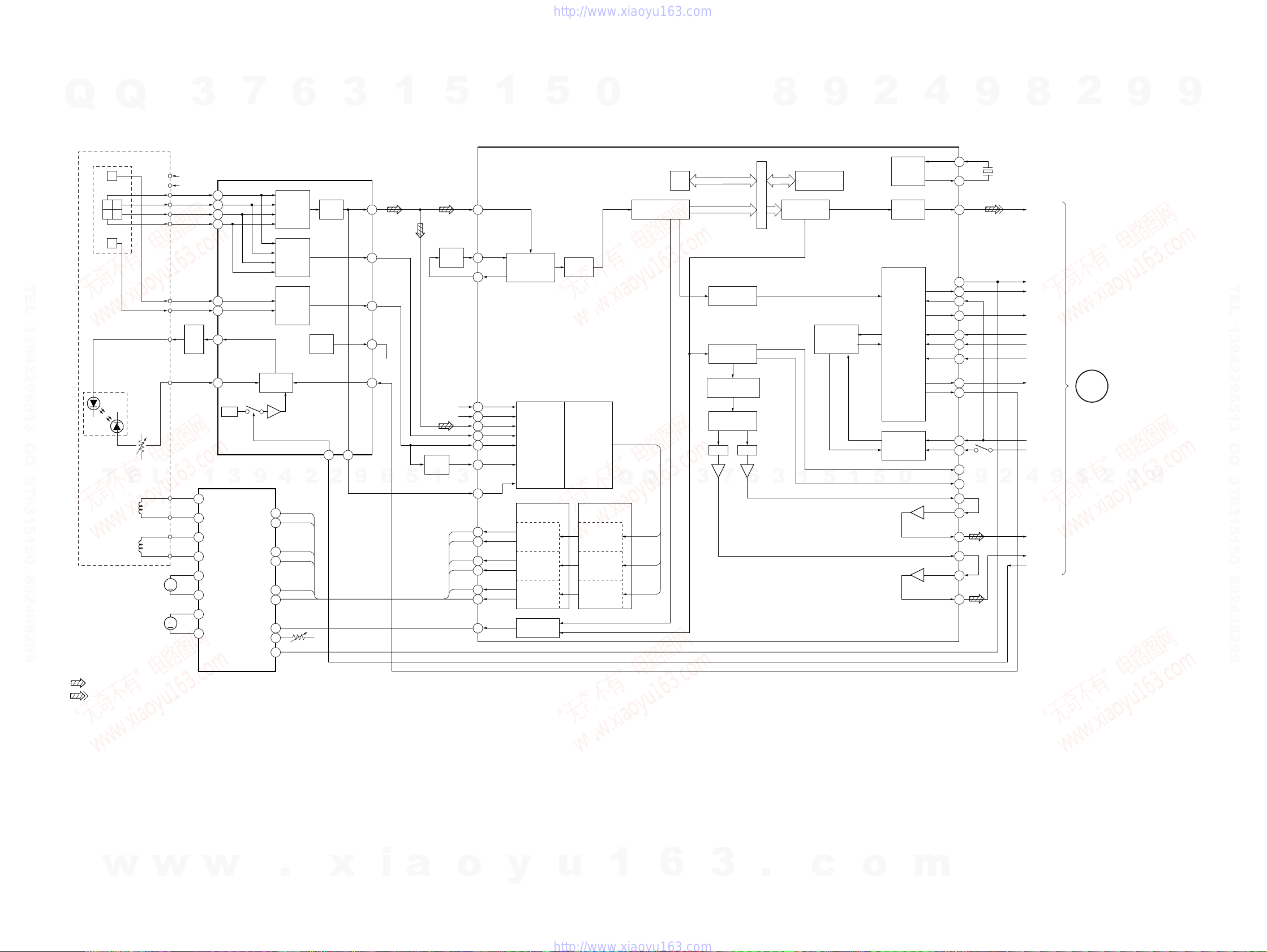
7-2. BLOCK DIAGRAMS
– BD (CD) SECTION –
Q
Q
OPTICAL PICK-UP BLOCK
(KSS-213B/K-N)
DETECTOR
E
ABC
D
F
3
VCC
VC
A
C
D
B
7
A
5
C
7
D
8
B
6
6
IC103
RF AMP
RF
SUMMING
AMP
FOCUS
ERROR
AMP
RF EQ
AMP
3
RF
16
FF
14 49
TEL 13942296513 QQ 376315150 892498299
9
CH2FIN
CH2RIN
CH1FIN
CH1RIN
CH3RIN
CH3FIN
CH4SIN
CH4BIN
MUTE
TRACKING
APCLD/PD
AMP
4
5
6
2
3
23
24
25
27
20
ERROR
AMP
TFDR
TRDR
FFDR
FRDR
SRDR
SFDR
BUFFER
HOLD SW
2
VC
TE
13
VC
REF
2
1521
LDON
9
12
22
6
• SIGNAL PATH
: CD
: Digital out
09
FD
PD
T
TRACKING
COIL
FOCUS
COIL
LASER
DIODE
POWER
E
LD
L
M102
SLED
MOTOR
M101
SPINDLE
MOTOR
E
F
LD
DRIVE
Q101
T+
T–
F+
F–
SD+
M
SD–
SP+
M
SP–
E
11
F
10
LD
3
PD
4
VREF
IC102
FOCUS/TRACKING COIL DRIVE
1
3
SPINDLE/SLED MOTOR DRIVE
CH2OUTR
11
CH2OUTF
12
CH1OUTF
14
CH1OUTR
13
CH3OUTF
17
CH3OUTR
18
CH4OUTF
15
CH4OUTR
16
VC
1
5
INTEGRATOR
1
5
INTEGRATOR
VC
3
1
IC101
DIGITAL SERVO
DIGITAL SIGNAL PROCESSOR
RF AC
51
ASY1
ASYMMETRY
CORRECTION
ASY0
48
VC
38
CE
42
RFDC
43
FE
TE
SE
CE
TFDR
TRDR
FFDR
FRDR
SRDR
SFDR
MDP
OPERATIONAL
AMPLIFIER
ANALOG
SWITCH
PWM
GENERATOR
TRACKING
PWM
GENERATOR
FOCUS
PWM
GENERATOR
SLED
PWM
GENERATOR
DIGITAL
CLV
39
41
40
42
30
31
32
33
29
28
26
5
DIGITAL
PLL
A/D
CONVERTER
SERVO DSP
TRACKING
0
SERVO
FOCUS
SERVO
SLED
SERVO
Q
16K
RAM
EFM
DEMODULATION
Q
SUBCODE
PROCESSOR
SERIAL IN
INTERFACE
OVER SAMPLING
DIGITAL FILTER
3rd ORDER
NOISE SHAPER
PWM PWM
3
7
6
8
DATA BUS
3
ERROR
CORRECTOR
D/A
INTERFACE
1
9
SERVO
AUTO
SEQUENCER
5
1
2
INTERFACE
INTERFACE
5
TIMING
LOGIC
DIGITAL
OUT
CPU
SERVO
0
4
XTA1
STAO
D OUT
XRST
SQSO
SQCK
SENS
DATA
XLAT
CLOK
SCOR
XLON
SCLK
SSTP
RMUT
LMUT
LMUT
AIN1
LOUT1
LOUT2
AIN2
LOUT2
8
66
67
60
3
1
2
8
5
6
7
20
14
9
27
79
80
70
71
72
77
76
75
9
S101
LIMIT SW
9
X101
16.9344MHz
2
8
DOUT
XRST
SQSO
SENS
DATA
XLT
CLOK
SCOR
SQCK
+5V
4
L OUT
R OUT
HOLD
2
SECTION
(Page 25, 27)
8
9
A
MAIN
2
9
9
9
TEL 13942296513 QQ 376315150 892498299
9
w
w
w
.
x
i
a
o
y
u
1
6
3
.
c
o
– 21 – – 22 –
m
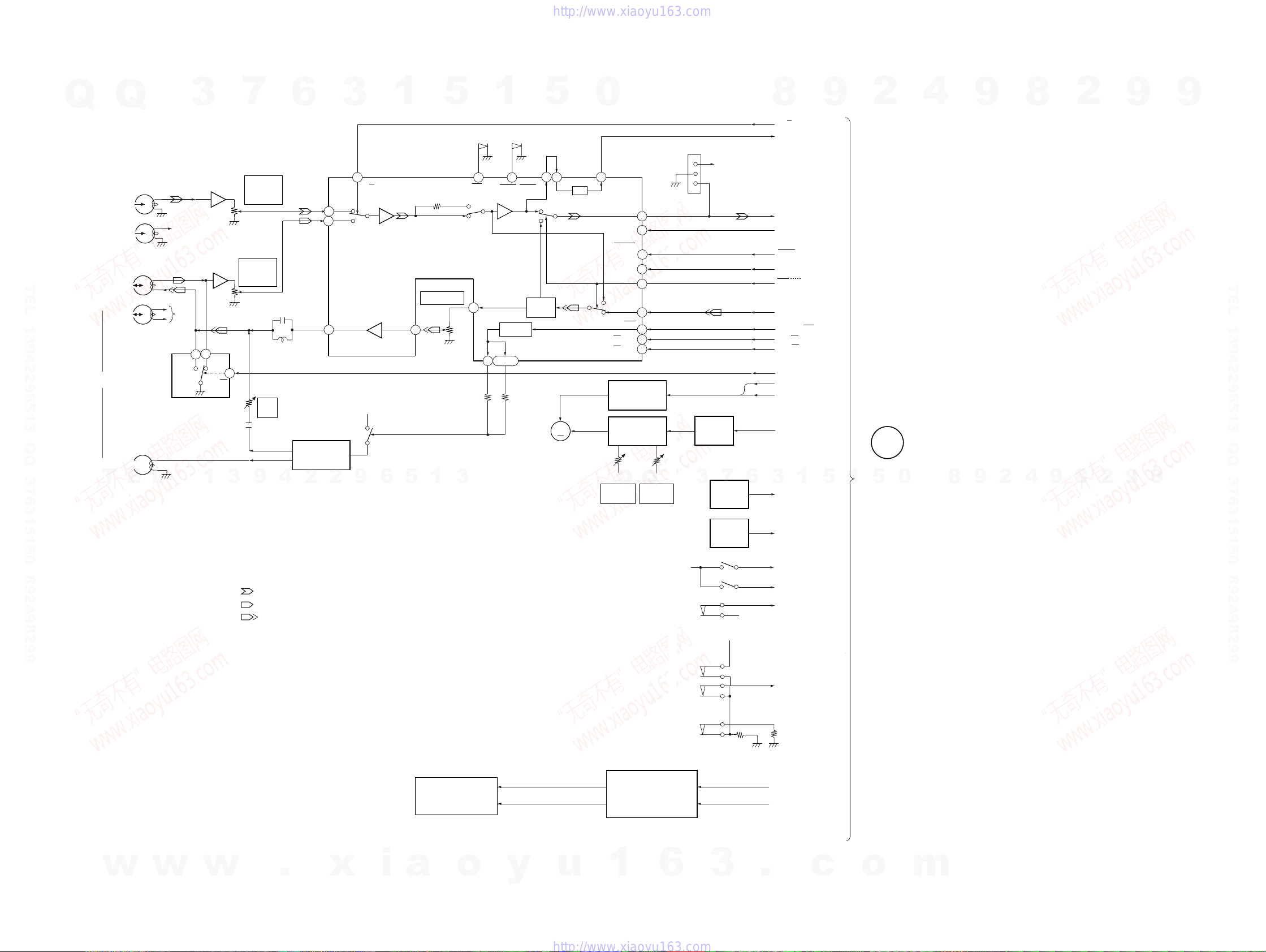
– DECK SECTION –
IC601
IC602
R
4
3
7
RV311
PLAYBACK
LEVEL
DECK A
RV301
PLAYBACK
LEVEL
DECK B
RV341
9
REC
BIAS
REC BIAS
6
4
48
46
36
BIAS OSC
T621, Q621, 622
2
2
3
16
A IN
B IN
EQOUT
9
Q
TEL 13942296513 QQ 376315150 892498299
HP101
PB HEAD
(DECK A)
REC/PB HEAD
(DECK B)
HRPE101
ERASE HEAD
T
Q
L
R
L
R
X
E
L
3
R CH
R CH
3
P
ERASE BIAS
IC611
1
REC/PB
1
PB-A/B
+7.5V
1
EQIN
Q623
6
5
38
5
DOLBY NR
IC301
RV301
REC LEVEL
1
120
70
3
S1004
A CrO
17
A 120/70
39
1
S1008
B CrO
2
19
B NORM/CROM/
METAL
DOLBY NR
RECOUT
BIAS SW
D
32
31, 33
PAS
DOL
M
CAPSTAN
MOTOR
2
M1
DOLBY
TYPE B
5
28
27
M
MS
0
26
PB OUT
LM ON/
NORM/
HIGH
NR ON/
PB
BIAS ON/OFF
RM ON/OFF
ALC ON/OFF
CAP MOTOR
CONTROL
Q336-343
RV1002
Q
NORMAL
SPEED
OFF
OFF
LIN
SPEED
CONTROL
Q1001
40
25
18
23
24
43
20
22
15
Q
RV1001
HIGH
SPEED
CN301
1
3
3
R CH
SWITCH
Q335
7
REEL
DETECT
IC1001
6
8
PB A/B
MS OUT
TC PB L
LM ON/OFF
NORM/HIGH
NR ON/OFF
REC/PB/PASS
TC REC L
BIAS ON/OFF
RM ON/OFF
ALC ON/OFF
RELAY
CAPM CNT1
CAPM CNT2
CAP M H / L
3
A SHUT
1
9
5
1
2
B
MAIN
SECTION
0
5
(Page 25,
26, 27)
HCD-DR4/DR5/DR6/DR440/W300/W5000/XB500
4
9
8
2
9
9
TEL 13942296513 QQ 376315150 892498299
9
9
2
8
9
4
2
9
8
REEL
DETECT
IC1002
S1001 (A PLAY)
• R CH : Same as L ch
• SIGNAL PATH
: PB (DECK A)
: PB (DECK B)
: REC (DECK B)
09
• PLUNGER SOLENOID is supplied
as the MECHANICAL BLOCK ASSY.
A DECK/
B DECK
PLUNGER
TRIGGER
MOTOR
CONTROL
Q331-334
+5V
S1003
(A HALF)
S1005
(REC A)
S1006
(B HALF)
S1009
(REC B)
S1002 (B PLAY)
+5V
+5V
B SHUT
A PLAY
B PLAY
A HALF
B HALF/REC A/REC B
B TRIG
A TRIG
w
w
w
.
x
– 23 –
i
a
o
y
u
1
6
3
.
c
o
m
– 24 –
HCD-DR4/DR5/DR6/DR440/W300/W5000/XB500
– MAIN (1/2) SECTION –
Q
TEL 13942296513 QQ 376315150 892498299
DECK
SECTION
(Page 24)
CD
SECTION
(Page 22)
POWER
SECTION
(Page 30,
32)
Q
VIDEO 2
IN
VIDEO
IN
PHONO
(L IN)
FM/AM TUNER
TUNER UNIT IS
SUPPLED AS THE
ASSEMBLED
BLOCK
B
A
MD (L IN)
C
R, AUDIO
T
E
(L IN)
V2, AU,
L-CH IN
FRONT
(L IN)
TC PB L
MIC-SIG
L
3
J804
J702
J701
ST-L
CD-L
J701
J701
1
J804
J703
7
IC191
AV SWITCH
6
IN3
IN4
IN1
1
B
A
2 3 5
46 45 28
IC181 SELECTOR
12
X0
3
9
X1
14
15
X2
A
10 9
46 45
X
B
VD OUT
13
C
4
6
10
2
IC601
PHONO AMP
3
2
3
1
9
69
IN A2
IN B2
68
IN C2
67
IN D2
66
65
IN E2
MIC IN
2
6
64
IN F2
1
IC101
SOUND PROCESSOR 1
REC B2
BUS OUT2
REC A2
5
1
BUF IN2
5
L+R
BBA2
BBB2
30
57
36
58
39
38
3
37
1
SWITCH
Q114
44 34
SWITCH
Q115
5
SWITCH
Q111
7
TC REC L
SWITCH
Q112
0
(TA-MUTE)
Q
Q
MUTE
SWITCH
Q113
3
7
6
8
3
J702
SPEANA
J701
L-CH SIG
TC REC L
1
9
VIDEO
OUT
REC OUT
5
D
E
B
1
2
DISPLAY
SECTION
(Page 33)
POWER
SECTION
(Page 29, 31)
DECK
SECTION
(Page 24)
0
5
4
8
9
9
2
8
4
9
2
8
2
9
9
9
TEL 13942296513 QQ 376315150 892498299
9
• R CH: Same as L ch
• SIGNAL PATH
: FM
: CD
: PB
: REC
: VIDEO/MD
09
w
w
w
.
– 25 –
x
i
a
o
MUTE
SWITCH
Q803
D807
RESET
SWITCH
Q802
y
MAIN CONTROL
IC501 (1/2)
6
LINE-MUTE
MUTE
SWITCH
Q804
u
F-RELAY
3
1
6
DBFB-H/L
PL-CLK
PL-DATA
PL-LAT
V-MUTE
SW-MODE
493-LAT
BASS FREQ
FUNC-SEL1
493-DATA
7
23
24
25
28
34
38
44
45
46FUNC-SEL0
47
48493-MUTE
22AC-CUT
3
7
23
24
25
28
34
38
44
45
46
47
48
DISPLAY
F
(Page 33)
(Page 29, 31)
o
SECTION
POWER
SECTION
m
.
RESET
F-RELAY
G
c
– 26 –
– MAIN (2/2) SECTION –
Q
Q
H
POWER
SECTION
3
HP.SW
(Page 30,
32)
TEL 13942296513 QQ 376315150 892498299
A
BD (CD)
SECTION
(Page 22)
T
E
L
B
DECK
SECTION
(Page 24)
B-HALF/REC A/REC B
FM/AM TUNER
TUNER UNIT IS
SUPPLED AS THE
ASSEMBLED
BLOCK
SCOR
SQ-DATA
SQ-CLK
CD-DATA
CD-CLK
SENS
HOLD
X-LAT
X-RST
TRAY.SENS
TBL.L
TBL.R
UP SW
LED
B TRG
A TRG
CAPM-CNT 2
CAPM-CNT 1
CAP-M-H/L
1
MS OUT
LM ON/OFF
REC/PB/PASS
NR ON/OFF
RM ON/OFF
BIAS ON/OFF
NORM/HIGH
PB A/B
ALC ON/OFF
B PLAY
A PLAY
A-HALF
B SHUT
A SHUT
RELAY
RDS-INT
RDS-DATA
ST-MUTE
STEREO
TUNED
ST-CE
ST-DOUT
ST-DIN
ST-CLK
7
3
IC781
OPTIC
TRANSMITTING
D.OUT
9
4
6
36 H/P IN
19
SCOR
32
SQ-DATA
33
SQ-CLK
35
CD-DATA
37
CD-CLK
56
SENS
57
HOLD
58
XLT
59
XRST
61
DISC-SENS
63
TBL-L
65
TBL-R
68
ENC 3/UP-SW
ENC 2/DISC-LED
69
72
B-TRG
73
A-TRG
74
CAPM-CNT 2
75
CAPM-CNT 1
76
CAP-M-H/L
2
77
AMS IN
78
TC-MUTE
79
R/PB/PAS
80
NR-ON/OFF
REC-MUTE
81
82
BIAS
83
EQ-H/N
84
PB-A/B
ALC
85
86
B-PLAY-SW
87
A-PLAY-SW
88
A-HALF
89
B-HALF
90
B-SHUT
91
A-SHUT
TC-RELAY
100
20
RDS-INT
21
RDS-DATA
49
ST-MUTE
50
STEREO
51
TUNED
52
ST-CE
53
ST-DOUT
54
ST-DIN
55
ST-CLK
3
MAIN CONTROL
IC501 (2/2)
2
9
1
STK-POWER
PROTECT
FL OFF
STBY RELAY
HP MUTE
WAKE UP
IIC-CLK
IIC-DATA
6
XC-IN
XC-OUT
X-OUT
X-IN
POWER
CD-POWER
27
42
43
93
18
29
30
5
10
11
13
15
HCD-DR4/DR5/DR6/DR440/W300/W5000/XB500
5
1
1
27
42
43
93
18
29
30
1
3
X501
X502
16MHz
2
5
1
5
W300,W5000,XB500
43
POWER
42
ECO
93
HP MUTE
1
STK POWER
27
PROTECT
30
DATA
29
CLOCK
18
WAKE UP
0
I
POWER
SECTION
(Page 29, 31)
J
DISPLAY
SECTION
(Page 33)
Q
Q
+UNREG, 12V
UN–10V
UN+10V
3
2
7
IC931
+10V
1 3
REG
IC932
+12V
1 3
REG
FAN DETECTOR
D405-409
IC951
–7V
2 3
REG
Q932
SWITCH
IC901
+7V
1 3
REG
6
IC911
+5V
1 3
REG
Q914
SWITCH
5
IC921
8
DETECTOR
3
Q905
1
SWITCH
2
Q931
SWITCH
Q901
SWITCH
2
9
Q931
Q932
SWITCH
Q932
SWITCH
Q902
5
SWITCH
SWITCH
2
SWITCH
FAN SWITCH
Q961, 963
1 3
1
Q901
Q902
SWITCH
Q913
2
IC933
+7V
REG
5
0
4
(LED–7V)
(LED+7V)
(D+5V SW)
(CD D+5V SW)
(CD A+5V SW)
PL A+10V
ST +10V
TC MOTOR+12V
M+7V (UNSW)
7V
A–7.5V
–V BIAS
–7
TC–7V
–7V
A+7.5V
+V BIAS
8
–7
TC–7V
–7V
LED 5V
LED 5V
D+5V UNSW
5V
AU D+5V
EVER +5V
D+5V (SW)
A+5V (SW)
9
FAN901
9
FAN
2
8
4
L
POWER
SECTION
2
8
9
(Page 29, 31)
2
9
9
9
TEL 13942296513 QQ 376315150 892498299
9
09
w
• R CH : Same as L ch
w
w
.
+5V
1 3
x
i
a
o
y
u
1
6
3
REG
.
c
Q921
SWITCH
o
m
– 27 – – 28 –
CD D+5V SW
CD A+5V SW
HCD-DR4/DR5/DR6/DR440/W300/W5000/XB500
– POWER SECTION – (DR4, DR5, DR6, DR440 model)
Q
Q
3
7
6
3
1
5
1
5
0
8
9
2
4
9
8
2
9
9
VOLUME
CONTROL
8
MUTE
Q834
6
5
MIC VOLUME
RV850
15
VOLUME
CONTROL
D802, 852
THERMAL
SENSOR
Q831-832
MIC AMP
J801
MIX MIC
MAIN 1
SECTION
(Page 26)
TEL 13942296513 QQ 376315150 892498299
MAIN 1
SECTION
(Page 26)
MAIN 2
SECTION
(Page 28)
G
E
L
F-RELAY
L-CH IN
EVER +5V
HP-MUTE
POWER AMP & VOLUME CONTROL
22
THERMAL
SENSOR
13
D804
HEAD PHONE
MUTE
Q833
IC850 (1/2)
IC801
12
CONTROL
ECHO CONTROL
9
LPF 2 IN
OP 2 IN
11
1
LPF 1 IN
PROTECT
DC AMP
Q433-434
L-CH THERMAL
PROTECT SWITCH
Q801
IC851
LPF 1 OUT
LPF 2 OUT
OP 2 OUT
LATCH
DRIVER
Q432
MIC LEVEL
RV851
2
8
10
RELAY
DRIVER
Q401-402
LATCH
DRIVER
Q437
PROTECT
SWITCH
Q439
MIC AMP
IC850 (2/2)
RY401
PROTECT
SWITCH
Q431
R-CH
MIC-SIG
MIC-SIG
J803
PHONES
HP.SW
TM401
L
FRONT
R
K
C
H
DISPLAY
SECTION
(Page 33)
MAIN 1
SECTION
(Page 25)
MAIN 2
SECTION
(Page 27)
TEL 13942296513 QQ 376315150 892498299
MAIN 2
SECTION
(Page 27)
09
T
E
L
I
• R CH : Same as L ch
• SIGNAL PATH
: FM
STK-POWER
PROTECT
1
3
9
DRIVE
MUTE
Q804
4
2
MUTE
SWITCH
Q803
2
9
6
VF (–35V)
5
1
SWITCH
Q904
3
–35V REG
Q903
+VH
RECT
D831
Q
Q
3
+UNREG. 12V
UN +10V
UN –10V
AC-L
AC-L
7
6
RECT
D833-836
RECT
D841-844
RECT
D832
3
VF
VF
1
POWER
1
5
TRANSFORMER
T951
5
MX ONLY
JW966
0
JW969
JW968
8
EXCEPT MX,AUS,TH
VOLTAGE
SELECTOR
VS901
AUS,TH
ONLY
9
2
9
9
2
8
9
4
AC
IN
w
w
w
.
– 29 – – 30 –
x
i
a
o
y
u
1
6
3
.
c
o
m
– POWER SECTION – (W300, W5000, XB500 model)
Q
Q
3
MIX MIC
7
J801
6
3
MIC AMP
IC850 (1/2)
1
MIC VOLUME
RV850
5
1
9
11
1
LPF 2 IN
OP 2 IN
LPF 1 IN
5
ECHO CONTROL
IC851
LPF 1 OUT
LPF 2 OUT
OP 2 OUT
0
2
8
10
MIC LEVEL
RV851
MIC AMP
IC850 (2/2)
8
9
2
HCD-DR4/DR5/DR6/DR440/W300/W5000/XB500
2
9
9
MIC-SIG
MIC-SIG
J803
4
PHONES
9
K
C
8
DISPLAY
SECTION
(Page 33)
MAIN 1
SECTION
(Page 25)
MAIN 1
SECTION
(Page 26)
TEL 13942296513 QQ 376315150 892498299
MAIN 1
SECTION
(Page 26)
MAIN 2
SECTION
(Page 28)
T
MAIN 2
SECTION
(Page 27)
09
G
E
L
E
L
I
• R CH : Same as L ch
• SIGNAL PATH
: FM
F-RELAY
EVER +5V
HP-MUTE
1
3
STK-POWER
PROTECT
W300, W5000, XB500
L-CH IN
POWER
ECO
9
W300
W5000
XB500
4
POWER AMP & VOLUME CONTROL
22
14
THERMAL
SENSOR
13
12
D804
HEAD PHONE
MUTE
Q833
MUTE
2
2
9
DRIVE
Q804
IC801
VOLUME
CONTROL
8
MUTE
CONTROL
Q834
MUTE
6
SWITCH
Q803
5
6
5
15
7
1
W300
W5000
XB500
3
VOLUME
CONTROL
D802, 852
THERMAL
SENSOR
Q831-832
PROTECT
DC AMP
Q433-434
L-CH THERMAL
PROTECT SWITCH
Q801
LATCH
DRIVER
Q432
Q
Q
MAIN 2
2
XB500 ONLY
230V
JW954
F951
120V
W300
W5000
ONLY
SECTION
(Page 27)
9
4
8
STANDBY
RELAY
RY901
2
9
TEL 13942296513 QQ 376315150 892498299
9
AC
IN
HP.SW
RECT
D833-836
5
RECT
D841-844
RECT
D832
RECT
D902-905
RECT
D907-910
SWITCH
Q904-905
SWITCH
Q906
TM401
TM402
0
L
FRONT
R
L
REAR
R
W300 ONLY
TRANSFORMER
8
RELAY CONTROL
SUB-TRANSFORMER
VF
RY401
RELAY
DRIVER
Q401-402
7
Q903
Q907
+5.6V
PROTECT
SWITCH
6
RECT
D831
Q431
3
+UNREG. 12V
1
+5.6V
3
REG
IC901
POWER
SWITCH
Q902
5
UN +10V
UN –10V
VF
LATCH
DRIVER
Q437
PROTECT
SWITCH
Q439
3
+VH
–VH
VF
–30V REG
SWITCH
R-CH
JW76
R-CH
1
+VL
–VL
1
H
POWER
T951
9
STANDBY
Q901
T901
w
w
w
.
x
i
a
o
y
u
1
6
3
.
c
o
m
– 31 – – 32 –
HCD-DR4/DR5/DR6/DR440/W300/W5000/XB500
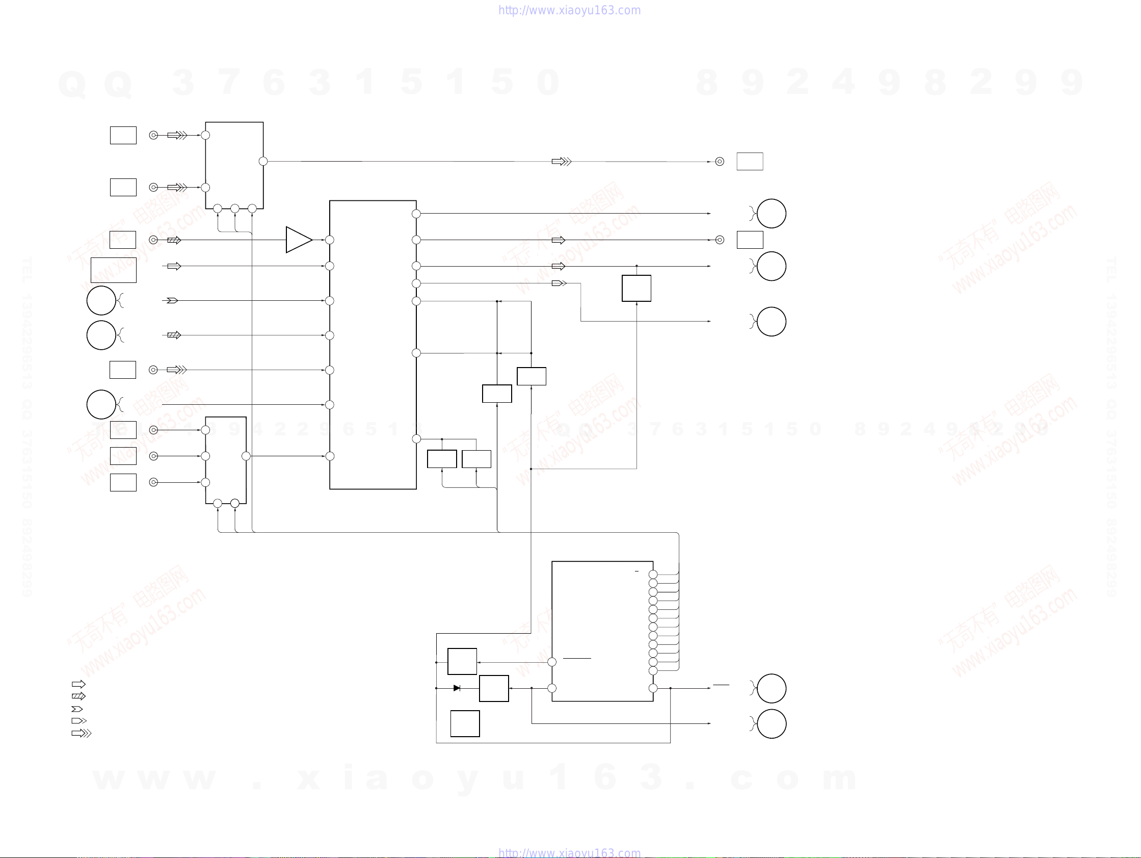
– DISPLAY SECTION –
Q
Q
3
7
6
3
TEL 13942296513 QQ 376315150 892498299
X601
12.5MHz
(Page
F
26)
E
RESET
DATA
CLOCK
WAKE UP
A –7V
A +7V
L
MIC–SIG
SPE–ANA
1
D671 – D675
3
9
REC LEVEL
OUTPUT
DISPLAY CONTROL (FOR MIC)
4
2
2
3
LINE NF
4
LINE IN
REC IN
6
REC NF
5
IC603
9
REC LEVEL
F06
F05
F04
F02
F01
6
11
12
13
14
16
17
MAIN 1 SECTION
MAIN 2 SECTION
(Page
27)
(Page 30, 32)
POWER SECTION
MAIN 1 SECTION
(Page 26)
J
T
K
D
1
5
70
72
73
78
79
22
1
21
20
19
18
17
16
5
X IN
X OUT
RESET
2
C DATA
I
2
C CLK
I
WAKE UP
3
ALL BAND
BPF 4
BPF 3
BPF 2
BPF 1
BPF 0
SEG-1
45 67
1
DISPLAY CONTROL
IC601
23
GR-3 14, 2
29VF40, 42
5
0
SIRCS
JOG A
JOG B
LED SCK
LED LATCH
LED DAT
D-SW
LED SEL
VOLUME A
VOLUME B
KEY 0
KEY 4
DAILY LED
REC LED
LED-EC0
GR-1
GR-15
GR-16
1
2
8
3
4
5
80
7
9
10
11
Q
15
74
75
77
43
28
27
Q
REMOTE
CONTROL
RECIEVE
IC602
S702
JOG
ROTARY
ENCODER
S691
OPEN
Q601 – Q603
LED POWER
SWITCH
S701
VOLUME
ROTARY
ENCODER
KEY MATRIX
Q605 – Q607
LED DRIVER
Q608 – Q610
DRIVER
0
4
8
9
9
2
8
4
D700
1
2
5
8
SERIAL
PARALLEL
CONVERTER
IC604
6
P3
P5
P7
P11
P12
P14
P1
P2
3
•
•
•
14
CLK
15
STB
13
DATA
6
D604 – D607
D604 – D607
7
3
D601 – D603
9
D611, D612, D616, D618 – D621,
D623 – D627, D635 – D638
1
5
•
7
9
•
20
22
17
•
19
D631, D632
5
1
9
2
8
2
9
9
9
TEL 13942296513 QQ 376315150 892498299
9
09
w
w
w
FLUORESCENT INDICATOR TUBE
.
– 33 – – 34 –
x
i
a
o
FL601
y
u
1
6
3
.
c
o
m
2.5V
APPROX 500mVp-p (PLAY)
2.5V
APPROX 200m Vp-p (PLAY)
HCD-DR4/DR5/DR6/DR440/W300/W5000/XB500
THIS NOTE IS COMMON FOR PRINTED WIRING
Q
TEL 13942296513 QQ 376315150 892498299
Q
BOARDS AND SCHEMATIC DIAGRAMS.
(In addition to this, the necessary note is printed
in each block.)
For schematic diagrams.
Note:
• All capacitors are in µF unless otherwise noted. pF: µµF
50 WV or less are not indicated except for electrolytics
and tantalums.
• All resistors are in Ω and 1/
specified.
¢
•
• C : panel designation.
• U : B+ Line.
• V : B– Line.
• H : adjustment for repair.
• Voltages and waveforms are dc with respect to ground
• Voltages are taken with a VOM (Input impedance 10 MΩ).
• Waveforms are taken with a oscilloscope.
• Circled numbers refer to wavefor ms.
• Signal path.
• Abbreviation
For printed wiring boards.
Note:
• X : parts extracted from the component side.
•
•
• b : Pattern from the side which enables seeing.
(The other layers' patterns are not indicated.)
: internal component.
Note:
The components identi-
fied by mark ! or dotted
line with mark ! are critical for safety.
Replace only with part
number specified.
under no-signal (detuned) conditions.
Voltage var iations may be noted due to normal produc-
tion tolerances.
Voltage var iations may be noted due to normal pro-
duction tolerances.
T
E
F : FM
g : VIDEO/MD
E : PB (DECK A)
d : PB (DECK B)
G : REC (DECK B)
J : CD
c : digital out
I : PHONO
CND : Canadian model.
AUS : Australian model.
®
¢
L
: Through hole.
: internal component.
3
4
W or less unless otherwise
Note:
Les composants identifiés par
une marque ! sont critiques
pour la sécurité.
Ne les remplacer que par une
piéce portant le numéro
spécifié.
1
3
7
9
4
6
2
2
3
9
1
6
5
1
5
3
1
5
0
Q
Q
WAVEFORMS
– BD (CD) SECTION –
1
IC101 ^§ XTAI
2
IC101 %¡ RF AC
3
4
5
7
3
IC101 @§ MDP
8
16.9MHz
(PLAY)
IC101 $¡ TE
IC101 #ª FE
3
6
7.5µsec
3.1Vp-p
1.2Vp-p
2.4Vp-p
1
9
5
1
2
5
0
4
– MAIN (2/5) SECTION –
9
1
2
– PANEL FL SECTION –
1
9
8
8
16MHz
IC501 !£ X-OUT
32.768kHz
IC501 !¡ XC-OUT
12.5MHz
IC601 &™ X-OUT
4
2
9
2
8
5.5Vp-p
5.2Vp-p
3.4Vp-p
2
9
9
9
TEL 13942296513 QQ 376315150 892498299
9
• Indication of transistor
C
EB
These are omitted
C
Q
These are omitted
EB
w
w
w
.
x
– 35 –
i
a
o
y
u
1
6
3
.
c
o
m
– 36 –
 Loading...