

Sony HCD-DP900P Schematic

HCD-DP900D
SERVICE MANUAL
Ver 1.2 2002.07
• HCD-DP900D is the tuner, deck,
DVD and amplifier section in MHCDP900D.
Model Name Using Similar Mechanism NEW
DVD DVD Mechanism Type CDM58D-DVBU9
Section Base Unit Name DVBU9
Optical Pick-up Name KHM-240AAA/CLNP
Tape deck Model Name Using Similar Mechanism HCD-DP800AV
Section T ape Transport Mechanism Type TCM-230AWR41/MWR41
E Model
Amplifier section
The following measured at AC 120, 220, 240 V,
50/60 Hz
DIN power output (rated) 130 + 130 watts
(6 ohms at 1 kHz, DIN)
Continuous RMS power output (reference)
180 + 180 watts
(6 ohms at 1 kHz, 10% THD)
Inputs
GAME IN: voltage 250 mV,
(phono jacks) impedance 47 kilohms
MD (VIDEO) IN: voltage 450 mV/250 mV,
(phono jacks) impedance 47 kilohms
OPTICAL IN:
(Square optical connector jacks, front panel)
wavelength ——
MIC: sensitivity 1 mV,
(Except for North impedance 10 kilohms
American and
European models)
(phone jack)
SPECIFICATIONS
Outputs
MD (VIDEO) OUT: voltage 250 mV
(phono jacks) impedance 1 kilohms
VIDEO OUT: max. output level
(phono jack) 1 Vp-p, unbalanced, Sync
negative, load impedance
75 ohms
S-VIDEO OUT: Y: 1 Vp-p, unbalanced,
(4-pin/mini-DIN jack) Sync negative,
C: 0.286Vp-p,
load impedance 75 ohms
PHONES: accepts headphones of
(stereo mini jack) 8 ohms or more
SPEAKER: accepts impedance of 6 to
16 ohms
SUB WOOFER: Voltage 1 V,
impedance 1 kilohms
— Continued on next page —
9-873-312-03
2002G0200-1
© 2002.07
MINI HI-FI COMPONENT SYSTEM
Sony Corporation
Home Audio Company
Published by Sony Engineering Corporation
HCD-DP900D
DVD player section
Laser Semiconductor laser
(DVD: λ =650 nm,
CD: λ =780 nm)
Emission duration:
continuous
Frequency response DVD (PCM 48 kHz):
2 Hz – 22 kHz = (±1 dB)
CD: 2Hz – 20 kHz =
(±1 dB)
Signal-to-noise ratio More than 90 dB
Dynamic range More than 90 dB
Video color system format
NTSC, PAL
DIGITAL OUT OPTICAL
(Square optical connector jack, rear panel)
Wavelength 660 nm
Tape player section
Recording system 4-track 2-channel stereo
Frequency response 40 – 13,000 Hz (±3 dB),
(DOLBY NR OFF) using Sony TYPE I
cassette,
40 – 14,000 Hz (±3 dB),
using Sony TYPE II
cassette
Tuner section
FM stereo, FM/AM superheterodyne tuner
FM tuner section
Tuning range 87.5 – 108.0 MHz
Antenna FM lead antenna
Antenna terminals 75 ohm unbalanced
Intermediate frequency 10.7 MHz
SAFETY-RELATED COMPONENT WARNING!!
COMPONENTS IDENTIFIED BY MARK 0 OR DOTTED LINE WITH
MARK 0 ON THE SCHEMATIC DIAGRAMS AND IN THE PARTS
LIST ARE CRITICAL TO SAFE OPERATION. REPLACE THESE
COMPONENTS WITH SONY PARTS WHOSE PART NUMBERS
APPEAR AS SHOWN IN THIS MANUAL OR IN SUPPLEMENTS
PUBLISHED BY SONY.
NOTES ON HANDLING THE OPTICAL PICK-UP
BLOCK OR BASE UNIT
The laser diode in the optical pick-up block may suffer electrostatic
break-down because of the potential difference generated by the
charged electrostatic load, etc. on clothing and the human body.
During repair, pay attention to electrostatic break-down and also
use the procedure in the printed matter which is included in the
repair parts.
The flexible board is easily damaged and should be handled with
care.
NOTES ON LASER DIODE EMISSION CHECK
The laser beam on this model is concentrated so as to be focused on
the disc reflective surface by the objective lens in the optical pickup block. Therefore, when checking the laser diode emission,
observe from more than 30 cm away from the objective lens.
Laser component in this product is capable
of emitting radiation exceeding the limit for
Class 1.
AM tuner section
Tuning range 531 – 1,602 kHz
(with the interval set at 9 kHz)
530 – 1,710 kHz
(with the interval set at 10 kHz)
Antenna AM loop antenna
Antenna terminals External antenna terminal
Intermediate frequency 450 kHz
General
Power requirements
Mexican model: 120 V AC, 60 Hz
Thailand model: 220 V AC, 50/60 Hz
Other models: 120 V, 220 V or
230 – 240 V AC,
50/60 Hz
Adjustable with voltage
selector
Power consumption 210watts
Dimensions (w/h/d) Approx. 280 x 360 x 365mm
Mass Approx. 12.5 kg
Supplied accessories: AM loop antenna (1)
FM lead antenna (1)
Remote commander (1)
Batteries (2)
Video cable (1)
Front speaker pads (8)
This appliance is classified as a CLASS 1 LASER product. The
CLASS 1 LASER PRODUCT MARKING is located on the rear
exterior.
CAUTION
Use of controls or adjustments or performance of procedures
other than those specified herein may result in hazardous radiation
exposure.
Notes on chip component replacement
• Never reuse a disconnected chip component.
• Notice that the minus side of a tantalum capacitor may be
damaged by heat.
Flexible Circuit Board Repairing
• Keep the temperature of soldering iron around 270˚C
during repairing.
• Do not touch the soldering iron on the same conductor of the
circuit board (within 3 times).
• Be careful not to apply force on the conductor when soldering
or unsoldering.
Design and specifications are subject to change without notice.
2
HCD-DP900D
Ver 1.2 2002.07
MODEL IDENTIFICATION
— BACK PANEL —
PARTS No.
MODEL
E model
MX model
SP, MY model
TH model
• Abbreviation
SP : Singapore model
MY : Malaysia model
TH : Thai model
MX : Mexican model
PARTS No.
4-236-825-0s
4-236-825-1s
4-236-825-2s
4-236-825-3s
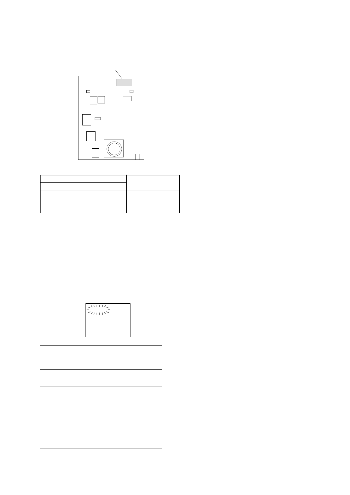
Self-diagnosis function
(When letters/numbers appear in the display)
When the self-diagnosis function is activated to prevent the system from
malfunctioning, a five-character service number (e.g., C 13 00) with a
combination of a letter and digits appears on the screen. In this case,
check the following table.
C:13:00
TABLE OF CONTENTS
1. GENERAL ·········································································· 5
2. DISASSEMBY···································································6
3. TEST MODE ···································································· 13
4. MECHANICAL ADJUSTMENTS ····························· 16
5. ELECTRICAL ADJUSTMENTS ······························· 17
6. DIAGRAMS
6-1. Circuit Board Location ················································· 21
6-2. Block Diagrams ···························································· 23
6-3. Printed Wiring Board RF-240 Section······················ 26
6-4. Schematic Diagram RF-240 Section ························ 27
6-5. Printed Wiring Board MB Section···························· 28
6-6. Schematic Diagram MB Section (1/5)······················ 30
6-7. Schematic Diagram MB Section (2/5)······················ 31
6-8. Schematic Diagram MB Section (3/5)······················ 32
6-9. Schematic Diagram MB Section (4/5)······················ 33
6-10.Schematic Diagram MB Section (5/5)·····················34
6-11. Schematic Diagram Driver Section ························ 35
6-12. Printed Wiring Board Driver Section······················ 35
6-13.Printed Wiring Board Main Section························· 36
6-14.Schematic Diagram Main Section (1/3)··················· 37
6-15.Schematic Diagram Main Section (2/3)··················· 38
6-16.Schematic Diagram Main Section (3/3)··················· 39
6-17.Printed Wiring Board DSP Section ··························40
6-18. Schematic Diagram DSP Section (1/2) ··················· 41
6-19. Schematic Diagram DSP Section (2/2) ··················· 42
6-20. Printed Wiring Board OPT/VIDEO Section··········· 43
6-21. Schematic Diagram OPT/VIDEO Section·············· 43
6-22. Printed Wiring Board Front Amp Section ···············44
6-23. Schematic Diagram Front Amp Section ················· 45
6-24. Schematic Diagram Surround Amp Section ··········· 46
6-25. Printed Wiring Board Surround Amp Section ········ 47
6-26. Printed Wiring Board Panel Section ······················· 48
6-27. Schematic Diagram Panel Section (1/2) ················· 49
6-28. Schematic Diagram Panel Section (2/2) ················· 50
6-29. Printed Wiring Board Leaf SW Section ··················51
6-30. Schematic Diagram Leaf SW Section····················· 51
6-31. Printed Wiring Board Trans Section ······················· 52
6-32. Schematic Diagram Trans Section·························· 53
6-33. IC Pin Function Description ······································· 54
6-34. IC Block Diagrams ····················································· 61
First three
characters of
the service
number
C 13
C 31
E XX
(XX is a number)
Cause and/or Corrective
Action
The disc is dirty
,Clean the disc with a soft
cloth (page 54).
The disc is not inserted correctly.
,Re-insert the disc correctly.
To prevent a malfunction, the
system has performed the self-diagnosis
function.
,Contact your nearest Sony
dealer or local authorized
Sony service facility and give
the 5-character service
number.
Example: E 61 10
7. EXPLODED VIEWS
7-1. Main Section································································· 65
7-2. Front Panel Section······················································· 66
7-3. Chassis Section ·····························································67
7-4. Tape Mechanism Deck Section-1 (TCM-230MWR41) 68
7-5. Tape Mechanism Deck Section-2 (TCM-230AWR41) 69
7-6. DVD Mechanism Deck Section (CDM58D-DVBU9) · 70
8. ELECTRICAL PARTS LIST ······································· 71
3

HCD-DP900D
Ver 1.2 2002.07
SERVICE POSITION
MB board
Jig (J-2501-155-A)
to RF240 board : CN004
Jig (J-2501-199-A)
to RF240 board : CN002
4
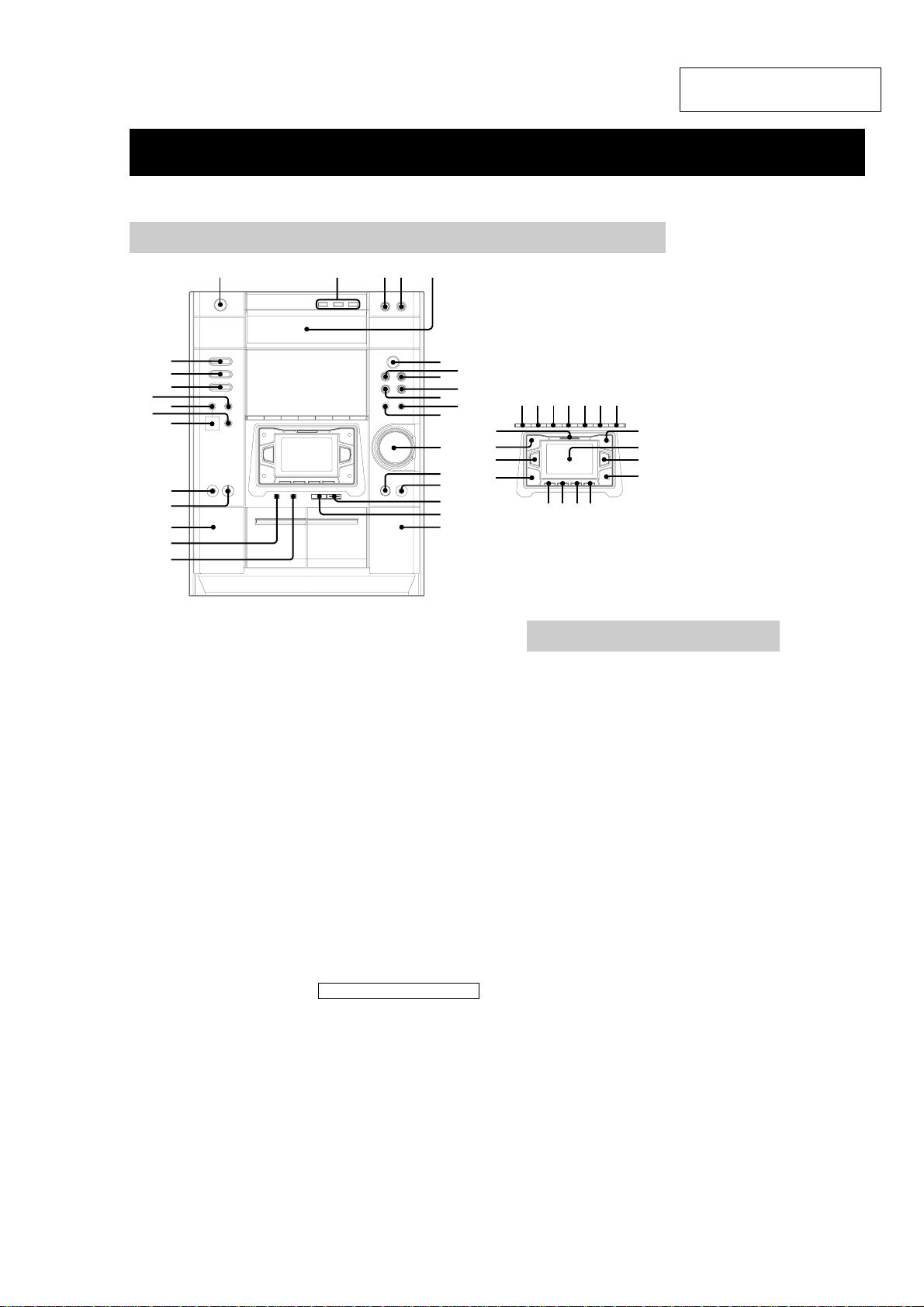
Parts Identification
The items are arranged in alphabetical order.
Main unit
SECTION 1
GENERAL
HCD-DP900D
Ver 1.2 2002.07
This section is extracted from
instruction manual.
1
e;
wl
wk
wj
wh
wg
wf
wd
ws
wa
w;
ql
2CH/MULTI rs (24, 46)
CD SYNC HI-DUB qj (43, 44)
CLOCK/TIMER SET ed (15, 45,
51)
DECK A Z wa (42)
DECK B Z qk (42)
digipad el (9, 24, 40, 47)
DIGITAL wh (52)
DIGITAL IN (OPTICAL) jack
wf (52)
DIRECTION eg (42–44, 50)
DISC 1–3 2 (23, 24)
DISC SKIP EX-CHANGE 3
(23, 24)
Disc tray 5 (23)
DISPLAY ea (16, 29, 30)
DOLBY NR eh (42–44)
DSP EDIT rj (47)
DVD e; (12, 25, 26, 34, 43, 44)
DVD DISPLAY eg (17, 28, 30)
DVD MENU ql (25)
EFFECT rd (47)
ENTER r; (14, 15, 25–27, 31,
32, 34–41, 44, 45, 47, 51)
FM MODE eh (41)
GAME wg (52)
GAME MODE rh (47)
GROOVE rf (46)
IR receptor qf
KARAOKE PON (Except for
North American and European
models) es (49)
MD (VIDEO) wj (52)
MIC jack (Except for North
American and European
models) wd (49)
2
MIC LEVEL control (Except for
North American and European
models) ws (49)
MOVIE MODE ek (47)
MULTI CHANNEL DECODING
indicator rl (46)
MUSIC MODE rk (47)
P FILE rg (48)
PHONES jack qg
PLAY MODE ej (23, 26, 27, 44)
PTY (European model only) eg
(41)
REC PAUSE/START qh (43, 44,
50)
REPEAT eh (28, 29)
SPECTRUM (North American
and European models only) es
(49)
TAPE A/B wk (42, 43)
TIMER SELECT ef (45, 51)
TITLE w; (25)
TOOL MODE ra (47)
TUNER/BAND wl (40)
TUNER MEMORY ej (40)
VOLUME control qd
BUTTON DESCRIPTIONS
@/1 (power) 1
Z OPEN/CLOSE (disc tray) 4
nN (play) 6
X (pause) 7
x (stop) 8
. (go back) q;
> (go forward) 9
m/– (rewind) qs
M/+ (fast forward) qa
3
45
6
8
q;
qs
qd
qf
qg
qh
qj
qk
7
9
qa
ea
rl
rk
rj
rh
esedefegeh
rf
rg
ej
ek
el
r;
ra
rdrs
Setting the time
1
Turn on the system.
2
Press CLOCK/TIMER SET.
When you set the time for the first time,
proceed to step 5.
3
Press . or > repeatedly to select
“CLOCK SET”.
4
Press ENTER.
5
Press . or > repeatedly to set the
hour.
6
Press ENTER.
7
Press . or > repeatedly to set the
minutes.
8
Press ENTER.
Tip
If you have made a mistake or want to change the
time, start over from step 2.
Note
The clock settings are canceled when you disconnect
the power cord or if a power failure occurs.
5

HCD-DP900D
)
SECTION 2
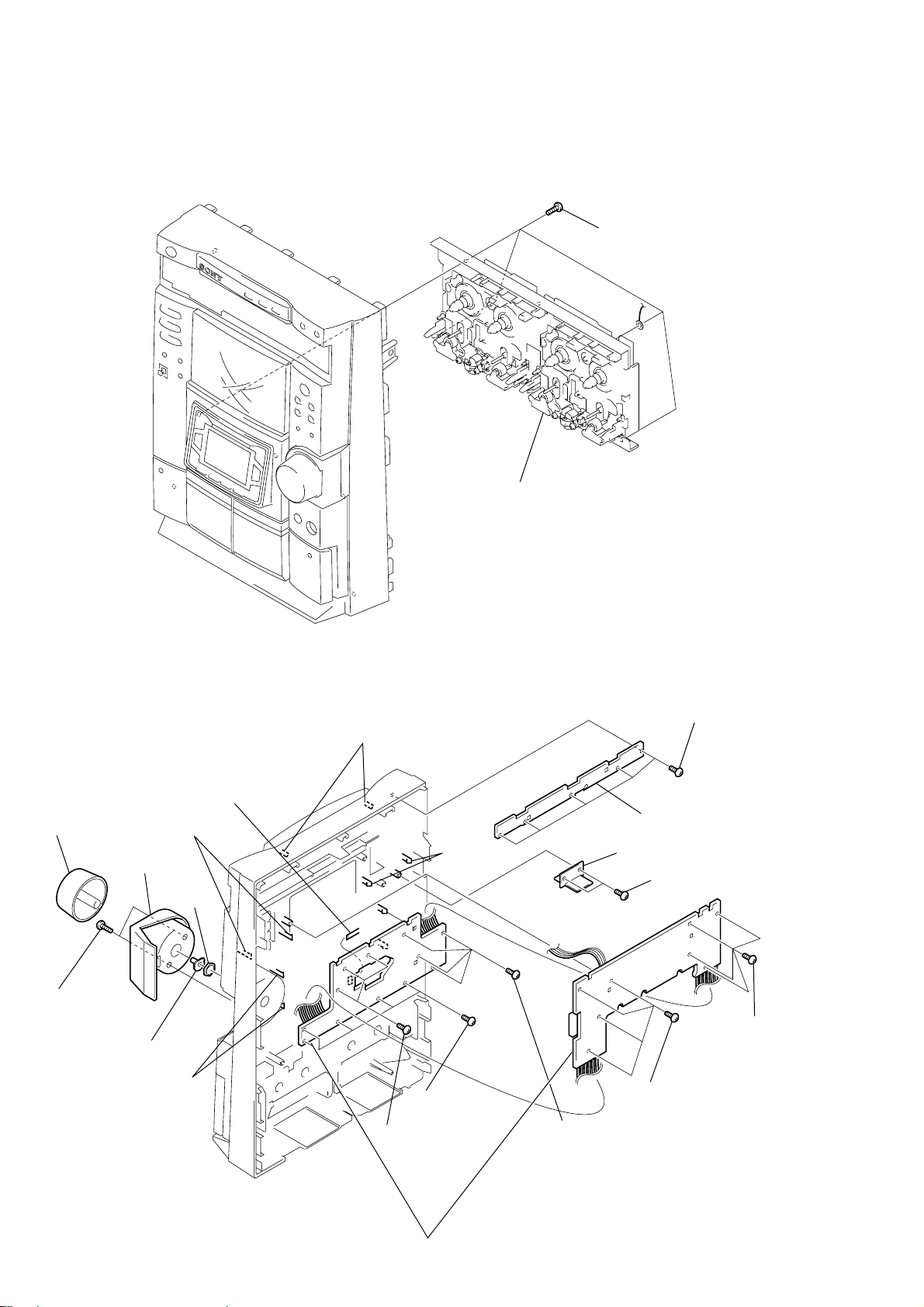
DISASSEMBLY
• The equipment can be removed using the following procedure.
Set Case (Top) Loading Panel Front Panel Section
Tape Mechanism Deck
(TCM-230AWR41/MWR41)
CD Panel board, Panel board, OPT IN Board
Chassis section
SUB Trans board, Back panel, Fan
Tnans board, Main board
DVD mechanism deck
DSP board, MB board, VIDEO board
(CDM58D)
Driver board, Motor board, Diode board, Sensor board, Tray, Sensor board
Note : Follow the disassembly procedure in the numerical order given.
2-1. CASE (TOP)
5
two screws (+BVTT 3
8
case
4
screw (case 3 TP2)
LEAF SW board, Head (A) board,
Head (B) board
Escutcheon pad
(With touch pad)
Front AMP board, Surround AMP board
RF-240 board, optical pick-up (KHM-240AAA)
6
×
8)
three screws (+BVTT 3
×
8)
3
two screws (case 3 TP2)
7
two screws
(+BVTT 3
2
screw (case 3 TP2)
1
two screws (case 3 TP2)
×
8
6
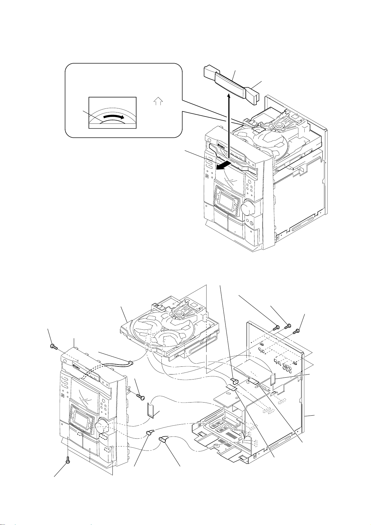
2-2. LOADING PANEL
DVD mechanism deck (CDM58D)
1
turn the pulley to the direction of arrow.
front panel side
4
pull-out the disc tray.
loading panel
HCD-DP900D
pulley
2
pull-out the disc tray.
2-3. FRONT PANEL SECTION, DVD MECHANISM DECK (CDM58D)
qa
connector (CN204)
3
qg
three screws (+BVTP 3
×8
)
qh
DVD mechanism deck (CDM58D)
3
screw (+BVTP 3
5
front panel section
4
three screws (+BVTT 3
×
10)
1
connector (CN601)
×
qf
two screws (+BVTP 3
2
screw
(+BVTP 3
7
connector (CN1)
8)
×
10)
6
flat type wire (CN1001)
8
connector (CN2)
qs
flat type wire
(CN501)
×8
)
qd
five screws
(+BVTP 3
9
flat type wire
(CN203)
chassis section
0
flat type wire
(CN502)
×8
)
7
HCD-DP900D
)
)
2-4. TAPE MECHANISM DECK (TCM-230AWR41/MWR41)
1
four screws (+BVTP 2.6
2
tape mechanism deck
(TCM-230AWR41/MWR41)
×
8
2-5. CD PANEL BOARD, PANEL BOARD, OPT IN BOARD
two claws
qf
flat type wire (CN108)
5
ring (vol)
×
8)
6
cover(vol)
two claws
two claws
7
nut
qa
five screws
(+BVTP 2.6
0
three
screws
(+BVTP 2.6
3
knob (vol)
4
two screws
(+BVTP 2.6
two claws
×
8)
×
1
five screws
(+BVTP 2.6
2
CD panel board
qh
OPT IN board
qg
two screws
(+BVTP 2.6
8
four screws
(+BVTP 2.6
9
five screws
8)
qs
four screws
(+BVTP 2.6
(+BVTP 2.6
×
8)
×
×
×
8)
8)
×
8
8)
qd
PANEL board
8

2-6. ESCUTCHEON PAD (WITH TOUCH PAD)
)
)
1
button (edit)
3
two screws
(+BVTP 2.6
touch pad
7
holder (pad)
6
two screws
(TPG +P 2
×
8)
×
8)
5
two screws
(TPG +P 2
4
escutcheon (pad)
8
three screws
(+BVTP 2.6
2
two screws
(+BVTP 2.6
×
8)
HCD-DP900D
×
8)
9
button (DSP
×
8)
2-7. SUB TRANS BOARD, BACK PANEL, FAN
1
connector (CN901)
2
connector (CN902)
5
SUB trans board
3
connector
(CN903)
qa
back panel
qf
fan
9
4
two screws
(+BVTP 3
0
two screws
(+BVTP 3
6
two screws
(+BVTP 3
qd
two screws
(+BVTP 3
7
two screws
(+BVTP 3
8
two screws
(+BVTP 3
rew (+BVTP 3
×
8)
×
8)
×
8
×
10
)
×
8)
×
8)
×
8)
qs
connector
(CN104)
9
HCD-DP900D
)
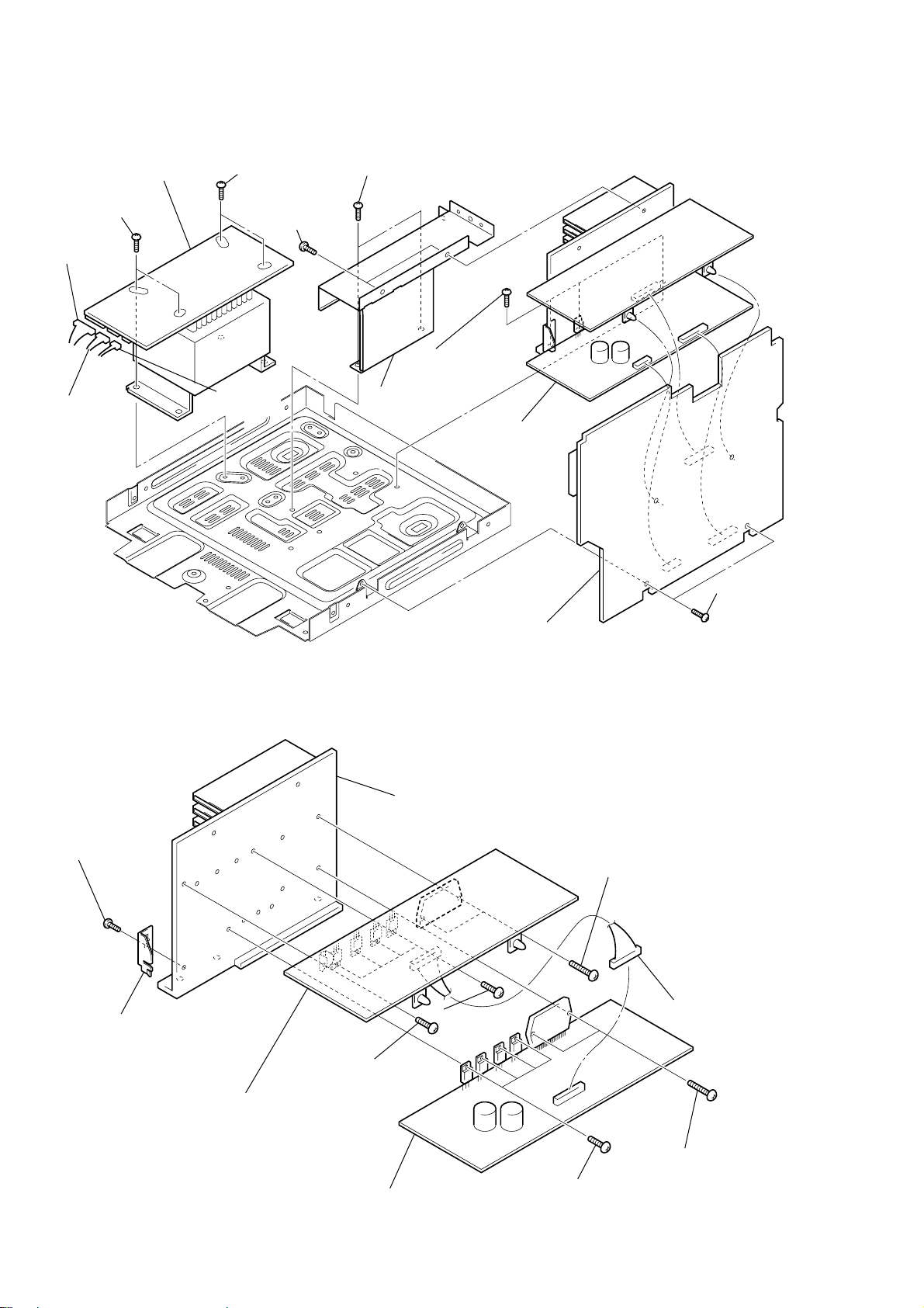
2-8. TRANS BOARD, MAIN BOARD
4
6
5
two screws
(+BVTT 4
1
connector
(CN914)
2
connector
(CN915)
TRANS board
×
8)
two screws
(+BVTT 4
7
two screws
(+BVTT 3
3
connector
(CN913)
×
8
two screws
×
8)
(+BVTP 3
9
8)
×
8)
0
two
screws
(+BVTP 3
cover (heat sink)
qa
SURROUND and
FRONT AMP
board ASSY
×
8)
2-9. FRONT AMP BOARD, SURROUND AMP BOARD
heat sink assy
1
screw
(+BVTT 3
2
bracket
×
8)
qd
8
four
screws
(+BVTT 3
MAIN board
×
8)
9
two
screws
(+BVTP 3
qs
two
(+BVTP 3
×
16)
3
connector (CN803
screws
×
8)
10
0
SURROUND AMP board
7
screw
(+BVTT 3
6
FRONT AMP board
×
8)
5
two
screws
(+BVTP 3
4
four
screws
(+BVTT 3
×
8)
×
16)

2-10. LEAF SW BOARD, HEAD (A) BOARD, HEAD (B) BOARD (TCM-230AWR41/MWR41)
Note: This illustration is for TCM-230MWR, but in case of TCM-230AWR, you can remove them in the same way.
1
five claws
2
LEAF SW board
3
remove the four solderings.
HCD-DP900D
5
HEAD (A) board
4
screw (+PTT 2
ground point
×
4),
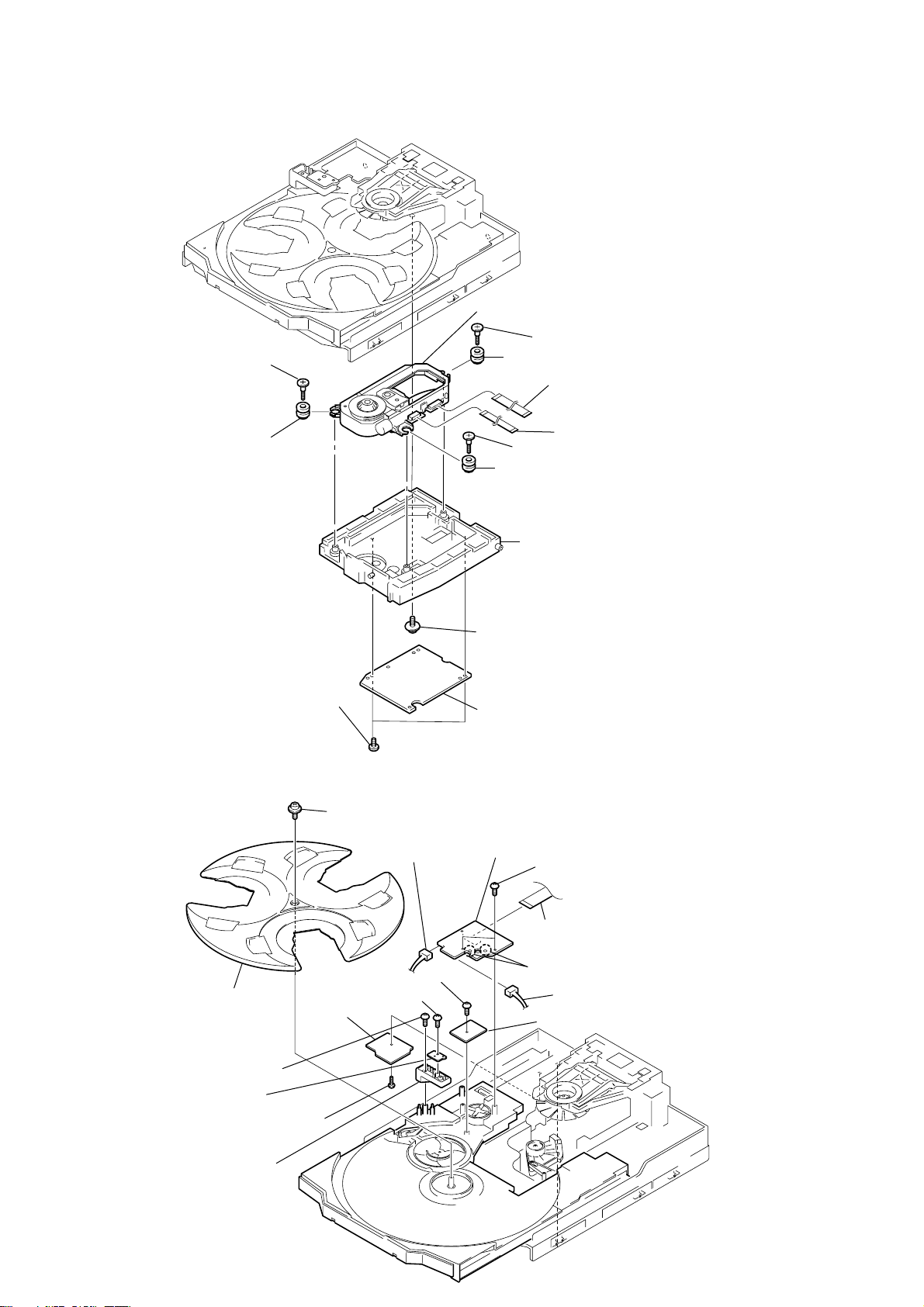
2-11. BASE UNIT, DSP BOARD, MB BOARD, VIDEO BOARD
6
HEAD (B) board
4
screw (+PTT 2
ground point
×
4),
DVD mechanism deck (CDM58D)
qd
screw (+BVTP 3X8)
qa
7
connector (CN202)
qs
VIDEO board
6
fiat type wire (CN011)
two screws (+BVTP 3X8)
0
MB board
9
two screws (+BVTP 3X8)
5
flat type wire (CN009)
1
two screws (+BVTP 3X8)
2
two screws (+BVTP 3X8)
4
flat type wire (CN010)
8
two screws (+BVTP 3X8)
qf
bracket (DVD)
3
DSP board
11
HCD-DP900D
)
2-12. RF-240 BOARD, OPTICAL PICK-UP (KHM-240AAA)
9
step screw (10)
qs
insulator
qd
optical pick-up (KHM-240AAA)
7
step screw (L)
0
insulator
5
flat type wire (26 core
6
flat type wire (9 core)
8
step screw (10)
qa
insulator
4
holder (DVD) assy
3
floating screw (+PTPWHM2.6)
1
two screws (+PTP 2.6X12)
2
RF-240 board
2-13. DRIVER BOARD, MOTOR BOARD, DIODE BOARD, TRAY, SENSOR BOARD
qd
qf
tray
screw (+PTPWH 2.6
8
qg
screw (+BVTP 2.6
9
screw (+BVTP 2.6
2
DRIVER board
connector(CN723)
×
×
×
8)
5
MOTOR board
3
two screws (+BVTP 2.6
6
8)
8)
flat type wire (CN721)
4
remove the two solderings of motor.
7
connector(CN722)
qh
SENSOR board
×
8)
12
qa
screw (+BVTP 2.6
0
DIODE board
1
screw (+BVTP 2.6
qs
BRCKET (SENSOR)
×
8)
×
8)

SECTION 3
TEST MODE
[Cold Reset]
• The cold reset clears all data including preset data stored in the
RAM to initial conditions. Execute this mode when returning
the set to the customer.
Procedure:
1. Press three buttons x , DISPLAY , and DISC 1
simultaneously.
2. The fluorescent indicator tube becomes blank instantaneously,
and the set is reset.
[Tuner Step Change] (Except for European and Middle Eastern
models)
• A step of AM channels can be changed over between 9 kHz and
10 kHz.
Procedure:
1. Press `/1 button to turn the set ON.
2. Select the function “TUNER”, and press TUNER/BAND button
to select the BAND “AM”.
3. Press `/1 button to turn the set OFF.
4. Press ENTER and `/1 buttons simultaneously, and the
display of fluorescent indicator tube changes to “AM 9 k STEP”
or “AM 10 k STEP”, and thus the channel step is changed over.
[MD/VIDEO Function Change]
• Change of function MD or VIDEO ( also the input level changes).
Procedure:
1. Press `/1 button to turn the set ON.
2. Press MD (VIDEO) and `/1 buttons simultaneously, and
the display of fluorescent indicator tube changes to “MD” or
“VIDEO”, and thus the channel step is changed over.
3. Press `/1 button to turn the set OFF.
HCD-DP900D
[MC Test Mode]
• This mode is used to check operations of the respective sections
of Amplifier, Tuner, and Tape.
Procedure:
• To enter MC Test Mode
1. Press `/1 button to turn on the set.
2. Press three buttons of x , DISPLAY and DISC 3
simultaneously.
3. Cursor segment flash on the FL display tube. The input
FUNCTION is changed to GAME.
* Check of Amplifier
Initial settings: Input , GAME
EQ , FLAT
Mode , MUSIC
VA C S , OFF
Output channel switching:
MUSIC key: L , LR , R through
MOVIE key: L , SL R , SR through
GAME key:L , L, SL, C R , R, SR, SW through
TOOL MODE key: L , CR , SW through
1. When VOLUME control knob is turned clockwise even slightly,
the sound volume increases to is maximum and a message
“VOLUME MAX” appears for two seconds, then the display
returns to the original display.
2. When VOLUME control knob is tuned counter-clockwise even
slightly, the sound volume decreases to its minimum and a
message “VOLUME MIN” appears for two seconds, then the
display returns to the original display.
[GC Test Mode]
• This mode is used to check the software version, FL tube, LED,
keyboard and VACS.
Procedure:
1. Press three buttons x , DISPLAY , and DISC 2
simultaneously.
2. LEDs and fluorescent indicator tube are all turned on.
3. When you want to enter the software version display mode,
press DISC 1 .The model number and destination are displayed.
4. Each time DISC 1 is pressed, the display changes stating from
MC version, GC version, DVD version, CDDM, CDMA,
CDMB, BDA, BDB version, ST version, TA version, TM
version, TC version, in this order, and returns to the model
number and destination display.
5. When DISC 3 is pressed while the version numbers are being
displayed except model number and destination, year, month
and day of the software creation appear. When DISC 3 is pressed
again, the display returns to the software version display. When
DISC 1 is pressed while year, month and day of the software
creation are being displayed, the year, month and day of creation
of the software versions are displayed in the same order of
version display.
6. Press DISC 2 button, and the key check mode is activated.
7. In the key check mode, the fluorescent indicator tube displays
“KOJOVO”. Each time a button is pressed, “KEY” value
increases.
However, once a button is pressed, _it is no longer taken into
account.
“VOL” value increases like 1, 2, 3...if rotating VOLUME knob
in “+” direction, or it decreases like 0, 9, 8...if rotating in
“_”direction.
8. Also when DISC 3 is pressed after lighting of all LEDs and FL
tubes, value of VACS appears.
9. To exit from this mode, press three buttons in the same manner
as step 1, or disconnect the power cord.
* Tuner function
1. In the test mode, the default-preset channel is called even when
the TUNER is selected and an attempt is made to call the preset
channel that has been stored in memory. (It means that the
memory is cleared.)
2. The minimum, center and maximum frequency of each band is
set then.
* Tape recording test
1. To enter the MC Test Mode.
2. Load tapes in both tape decks A and B.
3. Press the REC button to start recording.
4. Pressing M , m buttons during recording returns the tape
to the recording start position and stops it at this position.
5. Pressing the “High Speed Dubbing” key while playing back the
tape of deck B switches the playback speed between “Normal
Speed” and “High Speed”.
Note:
When the playback direction of the tape is set to other than “ONY
WAY”, the restriction on the number of times playback which can
be repeated will be cleared.
* AMS Test Mode
1. Set TAPE function
2. Select the desired loop by pressing PLAY MODE button.
Insert a test tape AMS-110A or AMS-120 to Deck A.
3. Press SPECTRUM or KARAOKE PON button to enter the
AMS test mode.
4. After a tape is rewound first, the FF AMS is checked, and the
mechanism is shut off after detecting the AMS signal the AMS
signal twice.
5. Then the REW AMS is checked and the mechanism is shut off
after detecting the AMS signal twice.
6. When the check is complete, a message of either OK or NG
appears.
* To return to normal mode again.
1. When you want to exit this mode, press `/1 button.
2. The cold reset is enforced at the same time.
13
HCD-DP900D
[Aging Mode]
This mode can for operation check of tape deck section and DVD
section.
• If an error occurred:
The aging operation stops and display then status.
• If no error occurs:
The aging operation continues repeatedly.
Procedure:
1. Press DVD button to select the function “DVD”.
2. Load the tapes into the decks A and B respectively.
3. Set a disk in “DISK1” tray.
4. Press PLAY MODE button to set the “ALL DISCS” mode,
and press the REPEAT button to “REPEAT” off.
5. Press three buttons of x , ENTER , and DISC SKIP/EXCHANGE simultaneously.
6. The aging mode is activated, if the indicator of DOLBY NR is
blinking.
7. To exit from the aging mode, operate the cold reset.
[Tape Deck Section]
• The sequence during the aging mode is following as below.
• If an error occurred, stop display that step.
Aging mode sequence (Tape deck section):
Rewind the tape A and B
“TAPE A AG-1”
Shut off
FWD play the tape A
“TAPE A AG-2”
2 minutes
Fast forward the tape A
“TAPE A AG-3”
Shut off or 20 seconds
RVS play the tape A
“TAPE A AG-4”
2 minutes
Rewind the tape A
“TAPE A AG-5”
Shut off
FWD play the tape B
“TAPE B AG-2”
Fast forward the tape B
“TAPE B AG-3”
RVS play the tape B
“TAPE B AG-4”
Rewind the tape B
“TAPE B AG-5”
14
2 minutes
Shut off or 20 seconds
2 minutes
Shut off
HCD-DP900D
[DVD Section]
• The sequence during the aging mode is following as below.
Aging mode sequence (DVD section):
Tray Turn
Disc 1 Chucking
TOC Read
Track 1 Play
2 seconds
Last Track Play
2 seconds
Error History Display
1. BD Error History Display
11 digits are displayed after the D character.
Example of display : D00209010100
1st digit : Indicates the error history number.
0 is the latest error
2nd to 3rd digits : Indicates details of the problem.
01 : Cannot focus
02 : GFS NG
03 : Start time over
04 : Focus deviates continuously
05 : Q code absent for some time
4th to 5th digits : Processing when problems occur
01 : Currently SHIP processing
02 : Currently POWER OFF processing
03 : Currently initializing
04 : Currently stopping
05 : Currently STOP operation processing
06 : Currently start processing
07 : Currently TOC reading
08 : Currently searching
09 : Currently playing
0A : Currently pausing
0B : Currently PLAY manual searching
0C : Currently PAUSE manual searching
6th to 7th digits : Operations currently performed for problems
which have occurred
8th to 9th digits : Rotation speed of DISC when problems occur
01 : x1 speed
02 : x2 speed
10th to 11th digits : Fixed at 00
2. CDM Error History <CDM58D Error History Display>
11 digits are displayed after the M character.
Example of display : M0FF400220000
1st digit : Indicates the error history number.
0 is the latest error
2nd to 3rd digits : Indicates the details of the problem.
01 : Initialization table is currently rotating 1
02 : Initialization table is currently rotating 2
03 : Initialization table is currently rotating 3
04 : Currently DISC SKIP in OPEN mode
05 : CLOSE table is currently rotating
06 : Chucking table is currently rotating
07 : Currently performing SHIP operations
08 : Currently performing release operations
09 : Currently performing POWER OFF
operations
4th to 5th digits : Processing when problems occur
01 : Currently performing SHIP operations
02 : Currently performing POWER OFF
operations
03 : Currently initializing
04 : Currently performing release operations
05 : Currently in chuck stop state
06 : Currently performing CLOSE operations
07 : Currently performing exchange CLOSE
operations
08 : Currently performing OPEN operations
09 : Currently performing OPEN POP UP
operations
0A: Currently performing exchange OPEN
operations
6 to 7th digits : Operations currently performed for problems
which have occurred
8th to 9th digits : Targets of processing when problems occur
Same as 4th to 5th digits
10th to 11th digits : Fixed at 00
[DVD and CD Ship Mode (No Memory Clear)]
• This mode moves the position to the position durable to vibration Use this mode when returning the set to the customer after
repair.
Procedure:
1. Press `/1 button to turn the set ON.
2. Press three DVD button and
3. After the “STANBY” display blinks six times, a message
“LOCK” is displayed on the fluorescent indicator rube, and the
DVD ship mode is set.
[DVD and CD Ship Mode (Memory Clear)]
• This mode moves the pickup to the position durable to vibration. Use this mode when returning the set to the customer after
repair.
Procedure:
1. Press
2. Press three buttons ENTER , DISC 1 , and DVD button
simultaneously.
3. After the “STANDBY” display blinks six times, a message
“LOCK” is displayed on the fluorescent indicator tube, and the
DVD ship mode is set.
button to turn the set ON.
`/1
button simultaneously.
`/1
15

HCD-DP900D
[VACS ON/OFF MODE]
• This mode is used to switch ON and OFF the VACS (Variable
Attenuation Control System).
Procedure:
Press three buttons x , ENTER and SPECTRUM or KARAOK
PON simultaneously.
[REPEAT 5 LIMIT OFF MODE]
• This mode is used to enable infinite repetitions.
Normally, the number of repetitions allowed is 5.
Procedure:
1. Press
2. Set the function “DVD”.
3. Press three burtons ENTER , DISC 3 , and x is simultaneously.
4. Infinite repetitions is enabled.
5. This state is maintained ( memorized ) until COLD RESET is
executed.
button to turn ON the power supply.
`/1
SECTION 4
MECHANICAL ADJUSTMENTS
Precaution
1. Clean the following parts with a denatured alcohol-moistened
swab:
record/playback heads pinch rollers
erase head rubber belts
capstan idlers
2. Demagnetize the record/playback head with a head
demagnetizer.
3. Do not use a magnetized screwdriver for the adjustments.
4. After the adjustments, apply suitable locking compound to the
parts adjusted.
5. The adjustments should be performed with the rated power
supply voltage unless otherwise noted.
Torque Measurement
Mode
FWD
FWD
back tension
REV
REV
back tension
FF/REW
FWD tension
REV tension
Torque meter
CQ-102C
CQ-102C
CQ-102RC
CQ-102RC
CQ-201B
CQ-403A
CQ-403R
Meter reading
3.06 N • m to 6.96 N • m
31 to 71 g • cm
(0.43 – 0.98 oz • inch)
0.19 N • m to 0.58 N • m
2 to 6 g • cm
(0.02 – 0.08 oz • inch)
3.06 N • m to 6.96 N • m
31 to 71 g • cm
(0.43 – 0.98 oz • inch)
0.19 N • m to 0.58 N • m
2 to 6 g • cm
(0.02 – 0.08 oz • inch)
6.96 N • m to 14.02 N • m
71 to 143 g • cm
(0.98 – 1.99 oz • inch)
9.80 N • m
100 g or more
(3.53 oz or more)
9.80 N • m
100 g or more
(3.53 oz or more)
16
SECTION 5
r
MAIN
board
CN301
set
test tape
P-4-A100
(10 kHz, –10 dB)
pin 1
oscilloscope
L-CH
R-CH
V
H
waveform of oscilloscope
in phase 45° 90° 135° 180°
good
wrong
pin 2
pin 3
L
R
forward
reverse
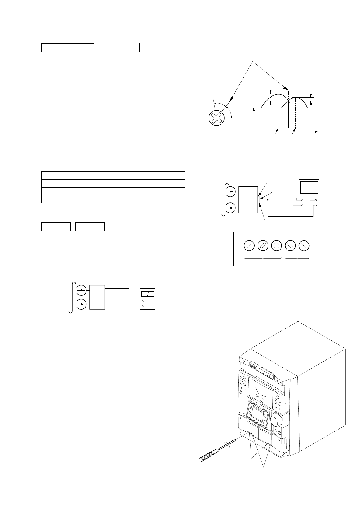
ELECTRICAL ADJUSTMENTS
HCD-DP900D
DECK SECTION
0 dB=0.775 V
1. Demagnetize the record/playback head with a head
demagnetizer.
2. Do not use a magnetized screwdriver for the adjustments.
3. After the adjustments, apply suitable locking compound to the
parts adjust.
4. The adjustments should be performed with the rated power
supply voltage unless otherwise noted.
5. The adjustments should be performed in the order given in this
service manual. (As a general rule, playback circuit adjustment
should be completed before performing recording circuit
adjustment.)
6. The adjustments should be performed for both L-CH and RCH.
7. Switches and controls should be set as follows unless otherwise
specified.
• Test Tape
Tape Signal Used for
P-4-A100 10 kHz, –10 dB Azimuth Adjustment
WS-48B 3 kHz, 0 dB Tape Speed Adjustment
P-4-L300 315 Hz, 0 dB Level Adjustment
Record/Playback Head Azimuth Adjustment
DECK A DECK B
2. Turn the adjustment screw and check output peaks. If the peaks
do not match for L-CH and R-CH, turn the adjustment screw
so that outputs match within 1dB of peak.
Output
level
within
1dB
L-CH
peak
R-CH
peak
within
1dB
Screw
position
L-CH
peak
Screw
position
R-CH
peak
3. Mode: Playback
Note: Perform this adjustments for both decks
Procedure:
1. Mode: Playback
test tape
P-4-A100
(10 kHz, –10 dB)
main board
CN301
Pin 3 (L-CH)
Pin 1 (R-CH)
set
main board
CN301
Pin 2 (GND)
level mete
+
–
4. After the adjustments, apply suitable locking compound to the
pats adjusted.
Adjustment Location: Playback Head (Deck A).
Record/Playback/Erase Head (Deck B).
17

HCDDP900D
r
Tape Speed Adjustment DECK B
Note: Start the Tape Speed adjustment as below after setting to the test
mode.
In the test mode, the tape speed is high during pressing
CD SYNC HI-DUB button.
Procedure:
1. Turn the power switch on.
2. Press x button, DISPLAY button and DISC 3 button
simultaneously.
(Cursor segment flash on the FL display tube.)
To exit from the test mode, press ?/1 button.
Mode: Playback
test tape
WS-48B
(3 kHz, 0 dB)
set
main board
CN301 (Pin 3 : L-CH)
frequency counter
+
–
(Pin 1 : R-CH)
1. Insert the WS-48B into the deck B.
2. Press Y button on the deck B.
3. Press CD SYNC HI-DUB button in playback mode.
Then at HIGH speed mode.
4. Adjust RV1001 on the LEAF SW board do that frequency
counter reads 6,000 ± 180 Hz.
5. Press CD SYNC HI-DUB button.
Then back to NORMAL speed mode.
6. Adjust RV1002 on the LEAF SW board so that frequency
counter reads 3,000 ± 90 Hz.
Adjustment Location: LEAF SW board
REC Bias Adjustment DECK B
Procedure:
INTRODUCTION
When set to the test mode performed in Tape Speed Adjustment,
when the tape is rewound after recording, the “REC memory mode”
which rewinds only the recorded portion and playback is set.
This “REC memory mode” is convenient for performing this
adjustment. During recording, the input signal FUNCTION will
automatically switch to VIDEO.
(If do not operation of stopped from recording complete, and rotette
of shuttle knob then rewind to recording start position.)
1. Press MD (VIDEO) button to select VIDEO. (This step is not
necessary if the above test mode has already been set.)
2. Insert a tape into deck B.
3. After press REC PAUSE/START button, press REC PAUSE/
START button, then recording start.
4. Mode: Record
MD/VIDEO (AUDIO) IN
1) 315 Hz
2) 10 kHz
AF OSC
attenuator
50 mV (–23.8 dB)
600 Ω
blank tape
CN-123
set
5. Mode: Playback
recorded
portion
level mete
Playback level Adjustment DECK A DECK B
Procedure:
Mode: Playback
test tape
P-4-L300
(315 Hz, 0 dB)
set
main board
CN301 (Pin 3 : L-CH)
(Pin 1 : R-CH)
level meter
+
–
Deck A is RV302 (L-CH), Deck B is RV303 (L-CH) so that
adjustment within adjustment level as follows.
Adjustment Level:
CN301 PB level: 334 to 375 mV (–6.8 dB ± 0.5 dB) level
difference between the channels: within ±0.5 dB
Adjustment Location: MAIN board
Sample Volue of Wow and Flutter: 0.3% or less W. RMS
(WS-48B)
set
CN301 (Pin 3 : L-CH)
(Pin 1 : R-CH)
+
–
6. Confirm playback the signal recorded in step 3 become
adjustable level as follows.
If these levels do not adjustable level, adjustment the RV304
(L-CH) and RV354 (R-CH) on the AUDIO board to repeat steps
4 and 5.
Adjustable level: Playback output of 315 Hz to playback output
of 10 kHz: 0±0.5 dB
Adjustment Location: MAIN board
REC Level Adjustment DECK B
Procedure:
INTRODUCTION
When set to the test mode performed in Tape Speed Adjustment,
when the tape is rewound after recording, the “REC memory mode”
which rewinds only the recorded portion and playback is set.
This “REC memory mode” is convenient for performing this
adjustment. During recording, the input signal FUNCTION will
automatically switch to VIDEO.
(If do not operation of stopped from recording complete, and rotate
of shuttle knob then rewind to recording start position.)
1. Press MD (VIDEO) button to select VIDEO. (This step is not
necessary if the above test mode has already been set.)
2. Insert a tape into deck B.
3. After press REC PAUSE/START button, press REC PAUSE/
START button, then recording start.
18

HCD-DP900D
r
4. Mode: Record
MD/VIDEO (AUDIO) IN
AF OSC
315 Hz, 50 mV (–23.8 dB)
600 Ω
blank tape
CS-123
attenuator
set
5. Mode: Playback
recorded
portion
set
CN301 (Pin 3 : L-CH)
(Pin 1 : R-CH)
level mete
+
–
6. Confirm playback the signal recorded in step 3 become
adjustable level as follows.
If these levels do not adjustable level, adjustment the RV301
(L-CH) and RV351 (R-CH) on the MAIN board to repeat steps
4 and 5.
Adjustable level:
CN301 PB level: 33.4 to 37.5 mV (–27.3 to –26.3 dB)
Adjustment Location: MAIN board
[MAIN BOARD] (Component Side)
T11
RV11
CN301
PB LEVEL (L)
(B)
REC LEVEL (R)
(B)
REC LEVEL (L)
(B)
PB LEVEL (L)
RV301
RV351
(A)
RV304
CN304
RV302
RV303
RV354
FM Tuned Level Adjustment
FM RF SSG
75
Ω
coaxial
set
Carrier frequency : 98 MHz
Modulation : AUDIO 1 kHz, 75 kHz
deviation (100%)
Output level : 25 dB (at 75
Ω
open)
FM ANTENNA terminal
(TM1)
Procedure:
1. Supply a 25 dB 98 MHz signal from the ANTENNA terminal.
2. Tune the set to 98 MHz.
3. Adjust RV11 to the point (moment) when the TUNED indicator
will change from going off to going on.
Adjustment Location: MAIN board
Null Adjustment
FM RF SSG
75 Ω coaxial
set
Carrier frequency : 98 MHz
Modulation : AUDIO 1 kHz, 75 kHz
deviation (100%)
Output level : 60 dB (at 75 Ω open)
FM ANTENNA terminal
(TM1)
Procedure:
1. Supply a 60 dB
98 MHz signal from the ANTENNA terminal.
2. Tune the set to 98 MHz.
3. Measure voltage between pin 22 and pin 3 of IC 11. Adjust
T11 ubtil the voltage becomes 0 V.
Adjustment Location: MAIN board
Adjustment Location
[MAIN BOARD] Component side
REC BIAS (L)
(B)
[LEAF SW BOARD] (Component Side)
TAPE SPEED
(NORMAL) (HIGH)
RV1002
RV1001
CN1001
REC BIAS (R)
(B)
T11
12
13
1
IC11
RV11
24
FM TUNED LEVEL
CN301
NULL
RV351
RV301
RV303
RV304
CN304
RV302
RV354
19
HCDDP900D
e
e
DVD SECTION
Note :
1. DVD Block is basically designed to operate without adjustment.
Therefore, check each item in order given.
2. Use HLX-504 (J-6090-088-A) or HLX-505 (J-6090-089-A)
unless otherwise indicated.
3. Use an oscilloscope with more than 10MΩ impedance.
4. Clean the object lens by an applicator with neutral detergent
when the signal level is low than specified value with the
following checks.
Video Level Adjustment (MB BOARD)
Purpose
This adjustment is made to satisfy the NTSC standard, and if not
adjusted correctly, the brightness will be too large or small.
Oscilloscop
75
Ω
set
J601
VIDEO OUTPUT
Procedure:
1. Connect oscilloscope to VIDEO output.
2. Load a disc (HLX-504 or HL-505) playback.
3. Adjust the RV501 to attain 1.0±0.1Vp-p.
3. Confirm that the S-Y level is 1.0 ± 0.1Vp-p.
1.0 ± 0.1 Vp-p
4. Connect oscilloscope to S-VIDEO output. (S-C teminal)
5. Connect that the S-C burst is 286 ± 50mVp-p.
286 ± 80 mVp-p
Adjustment Location
MB BOARD (SIDE A)
1.0 ± 0.1 Vp-p
(WHITE 75%)
S-terminal Output Check
Purpose
Check S-video output.
Oscilloscop
set
G
G
J602
S-VIDEO OUTPUT
75
Ω
Procedure:
1. Connect oscilloscope to S-VIDEO out. (S-Y teminal)
2. Load a disc (HLX-504 or HL-505) playback.
RV501
VIDEO LEVEL
Adjustment
CN404
CN011
IC103
IC503
CN008
CN103
20
SECTION 6
d
DIAGRAMS
HCD-DP900D
Ver 1.1 2002.03
6-1. CIRCUIT BOARD LOCATION
THIS NOTE IS COMMON FOR PRINTED WIRING BOARDS AND SCHEMA TIC DIAGRAMS.
(In addition to this, the necessary note is printed in each bloc k.)
Note on Schematic Diagram:
• All capacitors are in µF unless otherwise noted. pF: µµF
50 WV or less are not indicated except for electrolytics
and tantalums.
• All resistors are in Ω and 1/
specified.
f
•
• 5 : fusible resistor.
• C : panel designation.
• A : B+ Line.
• B : B– Line.
• H : adjustment for repair.
• Voltages and waveforms are dc with respect to ground
• Voltages are taken with a VOM (Input impedance 10 MΩ).
• Waveforms are taken with a oscilloscope.
• Circled numbers refer to waveforms.
• Signal path.
• Abbreviation
: internal component.
Note:
The components identified by mark 0 or
dotted line with mark 0 are critical for
safety.
Replace only with part number specified.
under no-signal (detuned) conditions.
Voltage variations may be noted due to normal produc-
tion tolerances.
Voltage variations may be noted due to normal production tolerances.
F : FM
f : AM
E : PB (DECK A)
d : PB (DECK B)
G : REC (DECK B)
c : digital out
g : MD (VIDEO)
MY : Malaysia model
SP : Singapore model
TH : Thai model
MX : Mexican model
EA : Saudi Arabia
4
W or less unless otherwise
Note on Printed Wiring Boards:
• X : parts extracted from the component side.
• : Pattern from the side which enables seeing.
• Indication of transistor.
C
These are omitted.
Q
B
CE
These are omitted.
Q
B
MOTOR board
DIODE board
SENSOR board
E
HEAD (A) board
HEAD (B) board
VIDEO board
SUB TRANS board
TRANS board
CD-PANEL board
DRIVER board
RF-240 board
LEAF SW board
MB board
DSP board
MAIN board
OPT IN board
SURROUND AMP boar
FRONT AMP board
PANEL board
2121
HCD-DP900D
p
r
WAVEFORMS
– MB BOARD –
IC102 8 XTO
1
IC701 2 INA
6
– PF-240 BOARD –
IC001 2 RFIN
1
– MAIN BOARD –
NO303 8 E-HOT
1
27MHz
IC102 9 512-2OUT
2
DVD STOP : 22.5792MHz
DVD PLAY : 24.576MHx
IC102 qd 33-2OUT
3
33.8688MHz
IC102 3 27-1OUT
4
4.0Vp-p
3.2Vp-p
3.2Vp-p
4.0Vp-p
H
IC701 4 INB
7
IC701 7 INC
8
H
IC701 9 OUT C2
9
1.3Vp-p
1.0Vp-p
H
1.3 Vp-p
2.6Vp-p
0.2V/div
100nsec/div
IC001 ra TE
2
0.5V/div
1msec/div
IC001 rs FE
3
0.1V/div
1msec/div
IC001 tl SIGO
4
0.72Vp-p
0.5Vp-p
0.3Vp-p
80kHz
T301 4
2
80kHz
IC401 qa XC-OUT
3
32.768kHz
IC401 qd X-OUT
4
35Vp-p
122Vp-p
3.2Vp-p
3.0Vp-p
IC103 ed X1
5
27MHz
16.5MHz
3.0Vp-p
H
IC701 qs OUT B2
0
IC701 qg OUT A1
qa
H
0.5V/div
100nsec/div
2.0Vp-p
H
– PANEL BOARD –
IC1101 is XO
1
1.3Vp-p
4MHz
1.4Vp-p
3.0Vp-
16MHz
IC51 ws XOUT
5
4.5MHz
3.8Vp-p
2222
6-2. BLOCK DIAGRAMS
– TUNER/DVD DSP SECTION –
OPTICAL PICK-UP
BLOCK
(KHM-240AAA)
SLA+
SLA-
SLB+
SLB-
SPM+
SPM-
19
14
13
12
11
15
16
17
18
2
25
26
21
22
24
37
36
35
34
32
31
30
29
27
28
VCC
DVDLD
CD LD
FCS+
FCS-
TRK+
TRK-
VC
A
B
C
D
E
G
H
RF
PD
SW
F
SLED
MOTOR
SPINDLE
MOTOR
+5V
Q001
LD
DRIVE
Q002
LD
DRIVE
M
M
IC001
RF AMP
VC
A
B
C
D
E
F
G
H
RF IN
DVD LD
CD LD
DVDPD
CDPD
LDSELO
MOTOR/COIL DRIVE
DO1+
DO1-
DO2+
DO2-
DO3+
DO3-
DO4+
DO4-
DO5+
DO5-
RFDCO
IC401
SDEN
SCLK
SWD
SRD
DFT
TZC
MIRR
MON
LDON
IN1+
IN1-
IN2+
IN2-
IN3-
OUT5
HCD-DP900D
DIGITAL SERVO
DIGITAL SIGNAL PROCESSOR
D/A CONV.
IC302 (1/2)
128
RFIN2
131
MDSO
MDPO
136
135
137
180
175
174
173
185
196
197
144
172
142
27
204
205
202
203
198
199
159
161
RFIN1
ADC1
ADC0
ADC2
GIO13
GIO8/SCK
GIO7/SDO
GIO6/SDI
DFCTI
TZC
MIRR
ADC7
GI05/PGIN
ADC5
SSTP
PDM2
PDM3
PDM0
PDM1
PWM0
PWM1
MDSO
MDPO
D OUT
DATA
BCK
LRCK
SDI0
SDI7
S DCKT
XSHD
XSAK
SDEF
MD0
MD15
MA0
MA9
XMWR
XRAS
XOE
XCAS
66
62
63
65
73
I
76
•
78
I
81
68
69
71
72
16
44
I
I
60
10
27
I
I
36
38
41
42
39
2-10
21-24
17
18
33
34
35
XLDON
8
IC303
SDRAM
I/O0
I
41-49
I/O15
A0
I
27-32
A9
WE
RAS
OE
UCAS
LCAS
B
DVD SYS
SECTION
(Page 24)
59
FE
42
TE
41
36PI
35PII
40TZIN
48
47
46
45
38
37
33
44
VCI
39
27
48
1
3
6
7
10IN4-
13IN5-
14
SSCS
SSCK
SSWD
SSRD
SSDFCTI
TZC
MIRR
SS MON
FDRV+
FDRV-
TDRV+
TDRV-
SLDA
SLDB
DIGITAL IN
22
23
25
26
31
I
34
•
36
I
39
41
44
45
43
OPTICAL
CDIN2I
CDIN1I
CDBCKI
CDLRCKI
DTI0
DTI7
ICLKI
ISTARTI
IVALI
IERRI
IC1195
DIGITAL
IN
IC503(1/2)
MPEG DECODER
COMPOUT
COUT
YOUT
AVDD
VREFI
SDDQ0
I
SDQ15
SDAD0
I
SDAD11
SPDIF
SDDQM0
SDWE0B
SDRAS0B
SDDQM1
SDCLKO
SDCKEO
SDCS0B
SDCS1B
DO
20
80
77
74
84
157
I
177
124
I
140
155
152
151
147
154
149
146
144
143
IC608
85
103
g
g
g
IC502
4
REG
RV501
16
12
DIGITAL AUDIO
IC604 (2/2)
DIN1
4
DIN0
3
INC
7
INA
2
INB
4
1
5
IC504,505
SDRAM
DQ0
I
2-12
39-49
DQ15
A0
I
19-24
27-32
A11
DQML
14
WE
15
CAS
16
RAS
17
DQMU
36
CLK
35
CKE
34
CS
18
CS
18
INTERFACE
SPDIF
IC701
VIDEO BUFFER
OUTC1
OUTC2
OUTA1
OUTA2
OUTCB1
OUTCB2
MUTE
+5V
IC609
2
10
g
9
15
g
14
13
g
12
1
OPTICAL
DIGITAL
CY
• RCH is omitted
• Signal Path
V MUTE
IN
due to same as LHC
: FM
: AM
: DVD
: DIGITAL OUT
: VIDEO
D
DIGITAL OUT
OPTICAL
J601
VIDEO
OUT
J602
S VIDEO
OUT
MAIN
SECTION
(Page 25)
FM 75Ω
AM
RV11
1
FM IF
11
AM/FM
24
OSC FM
12
VCO STOP
10
IF REQ MUTE
21
AM RF IN
22
AFC
23
AM OSC
VCC
9
AM/FM IF MPX
IC11
AM IF IN
AM MIX OUT
DECORDER
PLL IN OUT
DECORDER
STEREO
FM-DET
L OUT
R OUT
IN
TUNED
13
14
18
17
16
4
2
6
7
8
A+12V
R-CH
AMP
Q11
A+12V
IFT11
T11
LPF11
NULL
LPF
L-CH
A
MAIN
SECTION
(Page 25)
DI
DO
CL
CE
MASTER CONTROL
IC401(1/2)
23
ST-DOUT
25
ST-DIN
27
ST-CLK
CE
22
TUNED
88
STEREO
87
21
ST MUTE
TM1
G
8
FE2(AEP,UK)
ANT IN
IF OUT
OSC OUT
1
3
VT
4
CF1 CF2
+B
(FE2,3)
Q1
RF IF
AMP
Q2
A+12V
PLL
FM TUNED
LEVEL
A+12V
IC51
10
2
11
49
RB41
10
X51
4.5MHz
1
3
8
7
6
1
22
16
20
19
18
FM
XIN
XOUT
FM OSC
AOUT
AIN
PD
IF IN
AM OSC
12
FM
7
15
9VCO STOP
8IF REQ
DO
6DO
DI
DI
4DI
CL
CL
5
CE
CE
3
A+12V
2323

HCD-DP900D
– DVD SYS SECTION –
X102
27MHz
7
XTI
8
XTI
IC102
CLOCK OSC
27-1OUT
33-2OUT
33-1OUT
512-1OUT
IC302 (2/2)
DIGFITAL SERVO
DIGITAL SIGNAL PROCESSOR
D/A CONV.
TRS
TMS
TCK
TDO
XSRQ
191
192
194
195
70
122
TRST
TMS
121
120
TCK
118
TDI
IREQO
46
IC503 (2/2)
MPEG DECODER
IC006
MCKI
SCKI
102
109107 232221 25 18224
3
13
15
10
D0-7 HD0-7
CLKIN
2 - 9
HD8-15
A0-7
11-15
17-19
HA0-7
XINT
XARPIT
XSDPIT
HINT
XCS
XARPCS
HCS
XWAT
XWAIT
XSDPCS
ADDRESS BUS
MCKI
MCKI
180 29 12
MCKI
232-235,237-240
1-5,7-10
HD0-15
HAD0-7
218-215,213-210
208-205,203-200
198-195,193,192
HA0-21
HCSB
HRWB
220 221 223 224 226 227 228 229 190 191
XRD
XWRH
HIREQ0
XWAIT
XAVDIT
HWAITOB
DACK0
DM-REQ1
DM-ACK1
DACK1
DREQ0
DM-REQ00
DM-ACK0
DREQ1
HAD23
XAVDCS2
HAD22
XAVDCS3
+1.8V +3.3V
+1.8V +3.3V
+3.3V +5V
3
IC501
1
IC301
+1.8V
REG
+1.8V
REG
+3.3V
REG
1
2
14
TBL ADDRESS
SENSOR
S711
(BU UP/DOWN)
M721
TURN
MOTOR
S701
(OPEN/CLOSE)
D731
Q712
D+5V
Q711
IC701
MOTOR DRIVER
OUT1
4
2
OUT2
FIN
RIN
DATA BUS
HD8-11
HA0-3,19
85-100
18-15
D0-3 SHA0-3
TSW1
36
TSW2
35
7
9
33
TRMP
32
TRMM
CKMP
29
28
CKMM
5 - 2
1
SHA19
IC202
PGA
10 11
XIFCS
XRST
INT
CS5
CK
XIFCS
8
9
12
48
IC101
EEPROM
HD0-15 DQ0-15 A0-19HA0-21
77
CPUCK
XRST
35
INT3
19
65
CS6X
SDA
SCL
WP
102-109,111-118
1-5
WP
SCL
SDA
38 39 7 53 54 84
5
6
7
XRQ
XWRH
XRQ
CS0X
CS0X
XWRH
X1
X101
16.5MHz
XRAPIT
XSDPIT
XARPCS
INT1
INT2
IC103
DVD SYSTEM
CONTROL
X0
XSDPCS
CS4X
XWAIT
CS5X
XAVDIT
INT0
XWAIT
DREQ0
DACK0
DREQ0
DREQ1
DACK0
DREQ1
DKCK1
DACK1
XLD ON
XAVDCS2
60 6149 5046 4767 1662 6317 1870 71 58
CS2X
MAMUTE
XFRRST
INT4
SIO
SOO
SCO
XIFCS
XAVDCS3
CS3X
83
76
20
25
26
27
51
29-36
38-45
FLASH RAM IC107
XIFOK
TRST
1
3
2
4
6
5
12
11
13
IC106
25-16
10-1,48
XRD
CS0H
28 26 11
CE
OE
XIFOK
XFRRST
XIFINT
SIO
SOO
SCO
XIFCS
XLDON
XW0H
WE
MAIN
C
SECTION
(Page 25)
TUNER/DVD SYS
B
SECTION
(Page 23)
2424
– MAIN SECTION –
L-CH
TUNER
A
SECTION
J101
DECK-A
DECK-B
TC BLOCK
A120/70
B120/70
B SHUT
A SHUT
B PLAY
A PLAY
B HALF
A HALF
A TRG M+
B TRG M+
CAP M H/L
CAP M+
CN304
E+6V
L-CH
R-CH
R-CH
R-CH
R-CH
PB EQ
AMP
IC303
PB EQ
IC304
RV304
REC
BIAS(L)
E+6V
Q393,394
A TRIG
Q391,392
B TRIG
CAP MOTOR
SPEED CONT
Q396,397
CAP MOTOR
g
MD/VIDEO
(AUDIO)
HEAD
REC/PB
HEAD
ERASE
HEAD
L
R
PB
PB
RV302
LEVEL
AMP
E-6V
C332,L301
BIAS
TRAP
T301
DRIVE
DRIVE
Q395
DRIVE
• RCH is omitted due to same as LHC
• Signal Path
: PB (DECK A)
: PB (DECK B)
: REC (DECK B)
: FM
: CD
: MD(VIDEO)
: AM
TUNER/DVD DSP
SECTION
(Page 23)
RV303
1
2
3
BIAS
OSC
Q302,303
DVD SYS
SECTION
(Page 24)
PB
LEVEL
REC/PB SWITCH
IC302
Q301
E+6V
D
C
D1117
POWER
SWITCH
4
Q304,305
R CH
TC A+12V
Q141
DC
TC A+12V
BIAS
X401
32.768kHz
X402
16MHz
VMUTE
XIFOK
XFRRST
XIFINT
SIO
SOO
SCO
XIFCS SYS CS
Q1120
RED
DRIVER
IC1102
REMOTE
CONTROL
IR
RECEIVER
S1135
DISPLAY
S1115
POWER
48
46
36
33
32
90
89
57
56
91
70
69
50
52
54
55
10
11
13
15
48
43
40
42
36
35
37
19
97
4
73
A/N(L)
B/N(L)
EQ OUT(L)
BIAS(N)
BIAS(C)
A
B
B-SHUT
A-SHUT
B-PLAY
A-PLAY
B-HALF
A-HALF
TC-RELAY
A-TRIG
B-TRIG
CAP-M H/L
CAP M-CONT
XC-IN
XC-OUT
X-OUT
X-IN
VMUTE
SYS OK
SYS RST
SYS RQ
SYS IN
SYS OUT
SYS CLK
POWER
SIRCS
DISPLAY KEY
POWER KEY
BIAS
SW
HCD-DP900D
J601
FIP21
FIP59
FIP/LED5
PLAY1
PB6/AN13
PB6/AN14
PB7/AN15
XOUT
1
PHONES
I
XIN
T911
J1101
6-10
12-22
24-41
43-47
100
90
I
1-5
55
59
67
76
85
86
78
79
80
87
88
89LED1 FIP/LED4
52
53
54PB8/S10 LED13
83
82
L REC OUT
R-CH
R-CH
R-CH
NC
5.1CH
EFFECT
GROOVE
LED CTL
REC /
GAME
DIGITAL
VIDEO
TAPE A/B
TUNER
CD/DVD
DISC1
DISC2
DISC3
E,SP,MY
F911
F912
F913
F1
F2
D902-905
L IN1
L IN4
SWOUT
F1
ENTER
X1101
4.0MHz
JW906
E,SP,MY
E,SP,MY
JW905
TRANSFORMER
IC607(1/2)
MUTE
SWITCH
Q612
1
67
64
70
15
16
17
SOUND PROCESSOR
MAC IN
LIN2
LREC OUT1
LIN5
IC607(2/2)
SOUND PROCESSOR
B PLAY
B PLAY
B PLAY
IC603(2/2)
6
2
Q502
LINE
MUTE
Q501
RESET
SWITCH
RV1201
MIC-LEVEL
Q504-507
IC1201
MIC
AMP
POWER
MUTE
J1202
MIC
DECK PROC.
IC301
REC
70
PB
120
REC
EQ
38
RV301
REC(L)
LEVEL
39
B NORM/CROM/METAL
A120/70
17
19
67
MASTER CONTROL
PB A/B16NORM/HIGH
18
66
PB-A/B
IC401(2/2)
REC(L)
DOLBY
B
PB OUT(L)
DOL
PAS
BIAS ON/OFF
ALC ON/OFF15RM ON/OFF22NR ON/OFF23REC /PB/PASS24LM ON/OFF25MS OUT
20
68
65
61
60
59
58
ALC
BIAS
EQ -H/N
R/PB-PAS
REC-MUTE
NR-ON/OFF
SP PROTECT
FRONT RELAY
AMP-DATA
AMP-CLK
AMP-LAT
REAR-RELAY NC
STK-MUTE
LINE-MUTE
CODEC-SMUTE
DSP-CS
DIG-TX
DIG-CLK
DIR-STATE
DIR-RX
DIR-CS
IICDATA
IICCLK
M-RESET
DSP-RX
DSP-ACK
DSP-DECODE
DIR-UNLOCK
DVDPOWER
ACOUT
RESET
STBY RELAY
26
53
TC-MUTE
FAN
43
40
AMS-IN
86
84
1
2
3
85
72
71
79
81
5
7
77
78
76
94
30
29
41
6
80
82
75
38
100
12
8374
NC
32
COUT
NC
SLOUT
36
FLOUT
46 10
63
LREC OUT
66
LIN1
69
LIN4
28
SWOUT
MUTE
FRBB2
52
FRBB1
51
45
FLBB2
FLBB1
44
L REC IN
2
6
ADL+OUT
7
ADL-OUT
FLIN
9
L-RECIN
2
SWIN
13 24
C IN
12
PORT3
20
PORT1
18
21
PORT4
PORT5
22
BUFFER
5
1
X601
13.5MHz
DSP-DECODE
Q607
MUTE
Q611
Q604
DBFB
CONT
Q605
DBFB
CONT
IC605
MULTI-CHANEL AUDIO DECODE
30
LIN+
LIN-
29
27
LOUT1
25
LOUT2
LOUT3
23
LOUT3
PDN
17
SMUTE
3
Q613
RESET
SWITCH
IC604(1/2)
DIGITALAUDIO
INTERFACE
17
XSTATE
35
DO
37
CE
DI
36
CL
38
XOUT
21
XIN
22
IC603(1/2)
BUFFER
DSP-RX
12
DSP-DATA
10
8
DIR-UNLOCK
4
18
MCLK
DATA0
DATA1
DATA2
DATA3
LRCK
CKOUT
XMCK
AUDIO
ERROR
Q821,822
BCK
DATA
BCK
LRCK
IC801
POWER
AMP
12
Q823
MUTE
MUTE
SWITCH
39
4
9
6
7
8
5
16
14
15
13
20
24
34
13
11
9
3
11
+B
SCKOUT
14
BCK
20
SDI1
18
SDO1
23
SDO4
26
SDO3
25
19
LRCKO
GP10
67
BST
56
2
XRST
113
PM
36
HCS
33
HD IN
34
HCLK
30
SDI2
29
BCKI2
28
LRCKI2
22
KFSI2
12
MCLK2
9
MCLK1
69
GP8(AUDIO)
Q801
OVER LOAD
DETECTOR
Q816,817
THERMAL
DETECTOR
IC601
AUDIO DECODER
HACN
HDOUT
323568
D891
72
I
80
•
98
•
99
•
102
I
108
64
I
66
•
83
I
85
•
92
I
97
•
109
•
110
•
112
CSO
45
WEO
GP9(DECODE)
EXLOCK(ERROR)
59
GC+3.3V
Q835-837
PROTECT
DETECTOR
Q831,832
PROTECT
FEED BACK
16
I
13
•
10
I
7
•
38
I
35
•
32
I
29
20
I
18
•
2
I
4
•
1
•
5
•
21
•
24
•
42
I
44
•
27
I
25
61744
CONT
IC602
S-RAM
D15
D0
A15
A0
CS
WE
IC933
3
D606
D111
Q111-113
DRIVER
SWITCH
Q121
Q503
D+5V
1
R-CH
FAN
Q114
FAN
S1135
TOUCH
PANEL
DIVICE
S1136-1138,1140-1149
FUCTION
S1110-1114
S1129-1134,1139
FUCTION
S1116-1128
FUCTION
ENCORDER
VOLUME
+VH
-VH
+VL
-VL
Q833,834
PROTECT
DVD+12V
+4.5V
+2.6V
MC+9V
RELAY
DRIVE
IC921
3
Q881,882
REG
RY881
1
Q601
REG
IC610
REG
Q921-924
SWITCH
IC922
3
REG
MUTE
MUTE
SWITCHT
13
IC923
A+12V
1
REG
D+3.3V
IC931
3
D+5V
5VREG
(DVD)
D+5V
3
1
REG
IC932
3
(UNREG+16V)
1
REG
VP
(-30V)
IC934
3
1
REG
(UNREG+9V)
Q931,932
B+SWITCH
1
R-CH
KEY
KEY
KEY
S1101
D871
D1071
D950
D959
Q971
REG
IC501
3
RESET
EVER5.7V
AC1
AC1
AC2
AC2
AC3
AC3
AC4
AC4
TM801
M961
FAN
R CH
1
58
68
69
70
71
64
65
66
56
57
60
61
77
F916
F917
D830,831
D961,962
L
SPEAKER
R
DISPLAY CONTROL
IC1101
HEADPHONE
VL
VH
HL
HH
KEY0
PB7/SO1 LED11
PA3/AN3 LED10
KEY1
RLED5 FIP/LED0
KEY2
VOL 1A
VOL 1B
PB1/C11 LED14
IIC DATA
IICCLOCK
RSTX
D911
IC901
+5.7V
3
REG
RELAY
DRIVER
Q901
FRONT
FIP/LED20
PB4/AN2 LED9
LED4 FIP/LED1
LED1 FIP/LED2
LED1 FIP/LED3
PB0/IC1 LED15
POWER TRANSFORMER
F918
F919
J602
FLOURESCENT
INDICATOR TUBE
Q1107,1111
Q1108-1110,
Q1101-1106
Q1114-1116
RY901
JW901
TH
T901
SUB
FL1101
97 99
1112
LED
DRIVER
1113
LED
DRIVER
LED
DRIVER
LED
DRIVER
JW909
MX
L
OUT
R
L
IN
R
L
IN
R
SUB WOOFER
OUT
Q1123,1124
GRID
DRIVER
D1107,1111
D1108,1113
D1101-1106
D1114-1116
E,SP,MY
S901(1/2)
230-240
220
120
MX,TH
JW907
JW902
S901(2/2)
230-240
120
E,SP,MY
F2
1112
JW903
MD VIDEO
GAME
CN901
2
AC
IN
1
2525
HCD-DP900D
6-3. PRINTED WIRING BOARD – RF-240 SECTION – • See page 21 for Circuit Boards Location.
1
2
A
3 4 5 6 7
RF–240 BOARD (SIDE B) RF–240 BOARD (SIDE A)
8
9 10 11
B
CN004
C015
R045
R009
OPTICAL
R002
PICK–UP
BLOCK
KHM–240AAA
C
D
CN003
C005
CN001
C006
C002
C001
R003
C007
C008
C016
C019
C025
C022
1
16
C032
R038
C033
48
33
C038
C035
C040
R005
C043
C048
C046
R006
R037
C039
C047
64
49
C031
C027
C028
IC001
17
32
C036
C026
C034
B
A
MB
BOARD
(Page 28)
MB
BOARD
(Page 28)
C044
C018
R010
R011
C009
Q001
L001
C017
E
F
1-681-879-
11
(11)
D001
R007
C023
R008
C024
R025
Q002
R029
D004
C021
L002
R020
R023
CN002
1-681-879-
11
(11)
• Semiconductor
Location
Ref. No. Location
D001 E-7
D004 E-9
IC001 C-8
Q001 E-8
Q002 E-9
2626
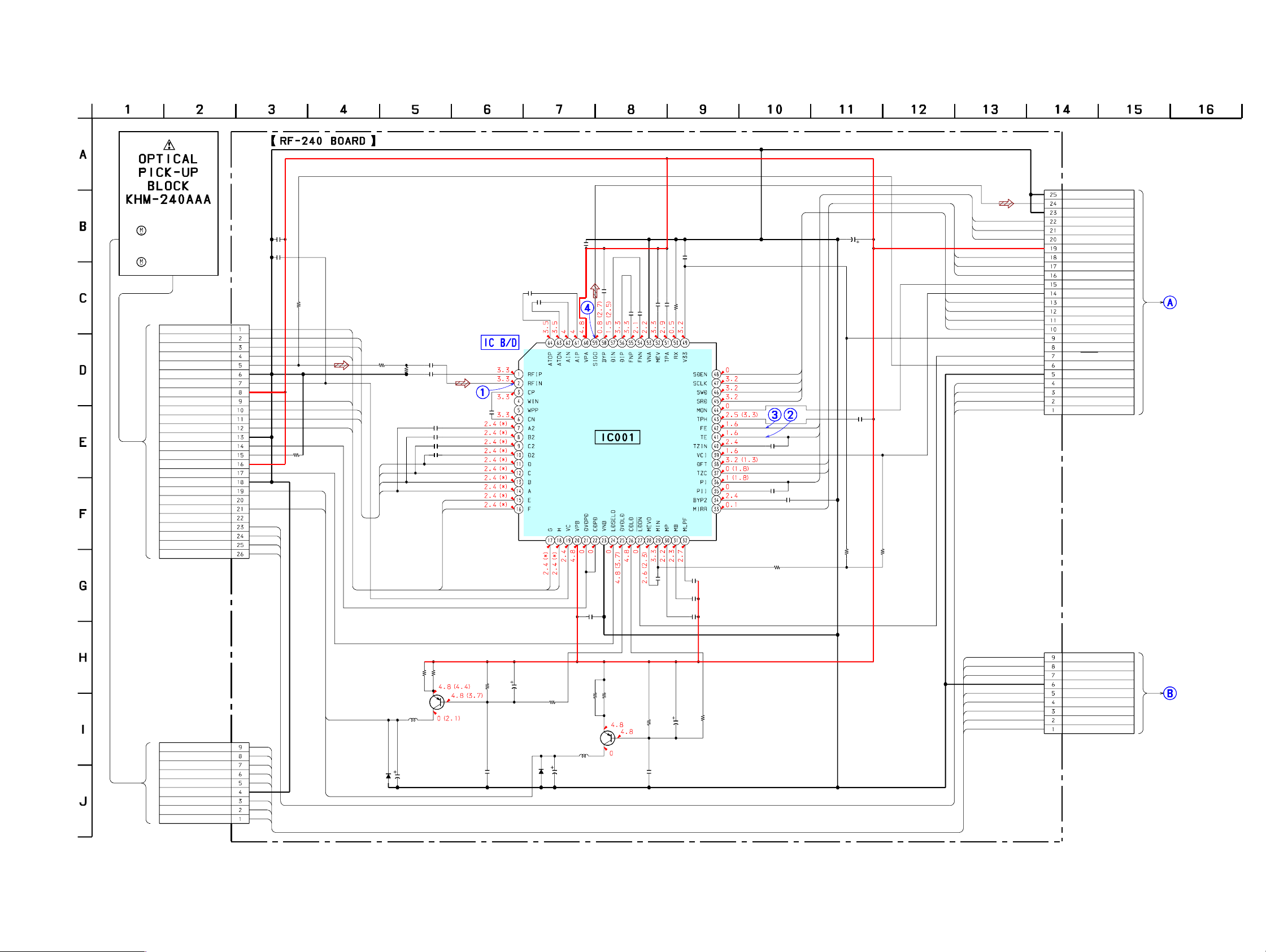
6-4. SCHEMATIC DIAGRAM – RF-240 SECTION – • See page 22 for Waveforms. • See page 64 for IC Block Diagrams.
SLED
MOTOR
SPINDLE
MOTOR
CN001
26P(1MMFFC)
LD GND
DVD LD
CN003
INLIM
SPM+
GND
VCC
GND
MOD
CD LD
FCS+
FCS-
TRK+
TRK-
9P
SLA+
SLB+
SLB-
SLA-
LED
GND
SPM-
C001
0.01
C002
0.01
C025
R002
100
DVD_LD
CD_LD
H
B
A
F
G
C
D
E
D001
1SS355TE-1
7
R045
100
R009
C015
4700p
1k
C016
4700p
C019
560p
C005
2200p
C006
2200p
C007
2200p
C008
R008
2200p
E
F
33
C018
0.001
R010
47k
C017
100
6.3V
D004
1SS355TE-1
7
D
C
B
A
R007
33
L001
47µH
Q001
2SB1132-T1
00-QR
LD DRIVE
C009
10
16V
H
B
A
F
RF
VC
G
C
D
E
PD
VR
SW
N.C
N.C
SLA+
SLB+
SLBSLA-
LED
INLIM
SPM-
SPM+
FCS+
FCSTRK+
TRK-
R003
100
DVD_LD
CD_LD
C022
R011
C027
0.01
0.01
0.1
0.1
G
H
R020
100
L002
47µH
C021
10
16V
C026
0.01
33
2SB1132-T1
LD DRIVE
Q002
00-QR
C028
IC001
SP3728AC
RF AMP
R023
33
0.1
C031
0.1
C032
C034
0.01
0.001
C033
R025
47k
C024
0.001
0.1
C035
12k
R037
C039
0.01
C023
6.3V
100
C040
150p
C038
0.047
C036
0.047
R029
HCD-DP900D
CN002
25P(1MMFFC)
GND
RF+
CN004
SPM+
SPM-
INLIM
GND
LED
SLA-
SLBSLB+
SLA+
9P
GND
PI
TE
FE
5V
MIRR
TZC
SSDFCTI
SS_MON
SVC
SSCK
SSWD
SSRD
SSCS
3.3V
RFTPON
LDON
RFMON
GND
FCS+
FCSTRK+
TRK-
MB
BOARD(1/5)
(Page 30)
MB
BOARD(1/5)
(Page 30)
SSCK
SSWD
SSRD
SSCS
MIRR
TZC
SSDFCTI
FCS+
FCSTRK+
TRK-
SPM+
SPM-
INLIM
LED
SLASLB-
SLB+
SLA+
PI
TE
FE
C044
10
16V
SSCS
SSCK
SSWD
SSRD
FE
TE
C047
0.1
SSDFCTI
TZC
PI
C048
0.01
MIRR
C046
0.01
R038
2.2M
100
C043
R005
100k
0.1
R006
27k
2727
 Loading...