

Page 1

DSC-V3
SERVICE MANUAL
Ver 1.0 2004.09
Revision History
Revision History
How to use
How to use
Acrobat Reader
Acrobat Reader
Link
Link
SPECIFICATIONS
SPECIFICATIONS
BLOCK DIAGRAMS
BLOCK DIAGRAMS
LEVEL 2
US Model
Canadian Model
AEP Model
UK Model
E Model
Hong Kong Model
Australian Model
Chinese Model
Korea Model
Tourist Model
Japanese Model
PRINTED WIRING BOARDS
PRINTED WIRING BOARDS
SERVICE NOTE
SERVICE NOTE
DISASSEMBLY
DISASSEMBLY
•For ADJUSTMENTS (SECTION 6), refer to SERVICE MANUAL, ADJ (9-876-762-51).
•For INSTRUCTION MANUAL, refer to SERVICE MANUAL, LEVEL 1 (9-876-762-41).
• Reference No. search on printed wiring boards is available.
• Note in Lens Frame Installation
• Note on Handling the Laser Diode
• The Method of Attachment of Harnesses
• HELP: Sheet attachment positions and procedures of processing the FLEXIBLE boards/harnesses are shown.
On the CH-146, SY-106 and DD-217 boards
This service manual procides the information that is premised the
circuit board replacement service and not intended repair inside the
CH-146, SY-106 and DD-217 boards.
Therefore, schematic diagram, printed wiring board and electrical
parts list of the CH-146, SY-106 and DD-217 boards are not shown.
The following pages are not shown.
FRAME SCHEMATIC DIAGRAM
FRAME SCHEMATIC DIAGRAM
SCHEMATIC DIAGRAMS
SCHEMATIC DIAGRAMS
REPAIR PARTS LIST
REPAIR PARTS LIST
DIGITAL STILL CAMERA
Schematic diagrams.................. Pages 4-9 to 4-34
Printed wiring boards ................ Pages 4-55 to 4-60
Waveforms ................................ Pages 4-69 and 4-70
Mounted parts location.............. Page 4-72
Electrical parts list ..................... Pages 5-10 to 5-12 and 5-15 to 5-18
DSC-V3
The above-described information is shown in service manual Level 3.
Sony EMCS Co.
2004I0500-1
©2004.9
Published by DI Technical Support Section9-876-762-31
Page 2

SPECIFICATIONS
x Camera
[System]
Image device
Total pixels number of camera
Effective pixels number of camera
Lens Carl Zeiss Vario-Sonnar
Exposure control
White balance
File format (DCF compliant)
Recording media
Flash Recommended distance (ISO set to
9.04 mm (1/1.8 type) color CCD
Primary color fi lter
Approx. 7 410 000 pixels
Approx. 7 201 000 pixels
4× zoom lens
f = 7 − 28 mm (34 − 136 mm when
converted to a 35 mm still camera)
F2.8 − 4.0
Automatic exposure, Shutter speed
priority, Aperture priority, Manual
exposure, Scene selection (7 modes)
Automatic, Daylight, Cloudy,
Fluorescent, Incandescent, Flash,
One-push
Still images: Exif Ver. 2.2 JPEG
compliant, RA
compatible
Movies: MPEG1 compliant
(Monaural)
“Memory Stick”
CompactFlash (Type I)
Auto):
0.4 to 3 m (15 3/4 inches to 118 1/8
inches) (W)
0.4 to 2.5 m (15 3/4 inches to 98 1/2
inches) (T)
W, TIFF, DPOF
[Input and Output connectors]
A/V OUT (MONO) jack (Monaural)
Accessory jack
USB jack mini-B
USB communication
Minijack
Video: 1 Vp-p, 75 Ω, unbalanced,
sync negative
Audio: 327 mV (at a 47 kΩ load)
Output impedance 2.2 kΩ
Mini-minijack (φ 2.5 mm)
Hi-Speed USB (USB 2.0 compliant)
[LCD screen]
LCD panel
Total number of dots
6.2 cm (2.5 type)
123 000 dots
TFT drive
[Power, general]
Used battery pack
Power requirements
Power consumption (during shooting
with LCD screen on)
Operating temperature
Storage temperature
Dimensions
Mass 410 g (14.5 oz) (including battery
Micr
Speaker Dynamic speaker
Exif Print Compatible
PRINT Image Matching II
PictBridge
NP-FR1
3.6 V
1.53 W
0°C to +40°C (+32°F to +104°F)
−20°C to +60°C (−4°F to +140°F)
119.8×72.0×63 mm (4 3/4×2 7/8×2
1/2 inches) (W/H/D, excluding
maximum protrusions)
pack NP-FR1, “Memory Stick” and
shoulder strap)
ophone
Electret condenser microphone
Compatible
Compatible
x AC-LS5/LS5B AC Adaptor
Input rating
Output rating
Operating temperature
Storage temperature
Dimensions
Mass Approx. 130 g (5 oz) excluding
100 V to 240 V AC, 50/60 Hz, 11 W,
0.16 A to 0.09 A
4.2 V DC, 1.5 A
0°C to +40°C (+32°F to +104°F)
−20°C to +60°C (−4°F to +140°F)
Approx. 48×29×81 mm (1 15/16×1
3/16×3 1/4 inches) (W/H/D,
excluding projecting parts)
power cord (mains lead)
x NP-FR1 battery pack
Used battery
Maximum voltage
Nominal voltage
Capacity 4.4
Lithium-ion battery
DC 4.2 V
DC 3.6 V
Wh (1220 mAh)
x Accessories
• AC-LS5/LS5B AC Adaptor (1)
• Power cord (mains lead) (1)
• NP-FR1 battery pack (1)
• Battery case (1)
• USB cable (1)
• A/V connecting cable (1)
• Shoulder strap (1)
• CD-ROM (USB driver SPVD-012) (1)
• CD-ROM (Image Data Converter Ver.2.0) (1)
• Operating instructions (1)
See page 5-19
Design and specifi cations are subject to change
without notice.
DSC-V3
— 2 —
Page 3
CAUTION
Use of controls or adjustments or performance
procedures other than those specified herein may
result in hazardous radiation exposure.
DSC-V3
Danger of explosion if battery is incorrectly replaced.
CAUTION
Replace only with the same or equivalent type.
SAFETY-RELATED COMPONENT WARNING!!
COMPONENTS IDENTIFIED BY MARK 0 OR DOTTED LINE WITH
MARK 0 ON THE SCHEMATIC DIAGRAMS AND IN THE PARTS
LIST ARE CRITICAL TO SAFE OPERATION. REPLACE THESE
COMPONENTS WITH SONY PARTS WHOSE PART NUMBERS
APPEAR AS SHOWN IN THIS MANUAL OR IN SUPPLEMENTS
PUBLISHED BY SONY .
SAFETY CHECK-OUT
After correcting the original service problem, perform the following
safety checks before releasing the set to the customer.
1. Check the area of your repair for unsoldered or poorly-soldered
connections. Check the entire board surface for solder splashes
and bridges.
2. Check the interboard wiring to ensure that no wires are
"pinched" or contact high-wattage resistors.
3. Look for unauthorized replacement parts, particularly
transistors, that were installed during a previous repair. Point
them out to the customer and recommend their replacement.
4. Look for parts which, through functioning, show obvious signs
of deterioration. Point them out to the customer and
recommend their replacement.
5. Check the B+ voltage to see it is at the values specified.
6. FLEXIBLE Circuit Board Repairing
•Keep the temperature of the soldering iron around 270°C
during repairing.
• Do not touch the soldering iron on the same conductor of the
circuit board (within 3 times).
• Be careful not to apply force on the conductor when soldering
or unsoldering.
ATTENTION AU COMPOSANT AYANT RAPPORT
À LA SÉCURITÉ!
LES COMPOSANTS IDENTIFÉS P AR UNE MARQUE 0 SUR LES
DIAGRAMMES SCHÉMA TIQUES ET LA LISTE DES PIÈCES SONT
CRITIQUES POUR LA SÉCURITÉ DE FONCTIONNEMENT. NE
REMPLACER CES COMPOSANTS QUE PAR DES PIÈSES SONY
DONT LES NUMÉROS SONT DONNÉS DANS CE MANUEL OU
DANS LES SUPPÉMENTS PUBLIÉS PAR SONY.
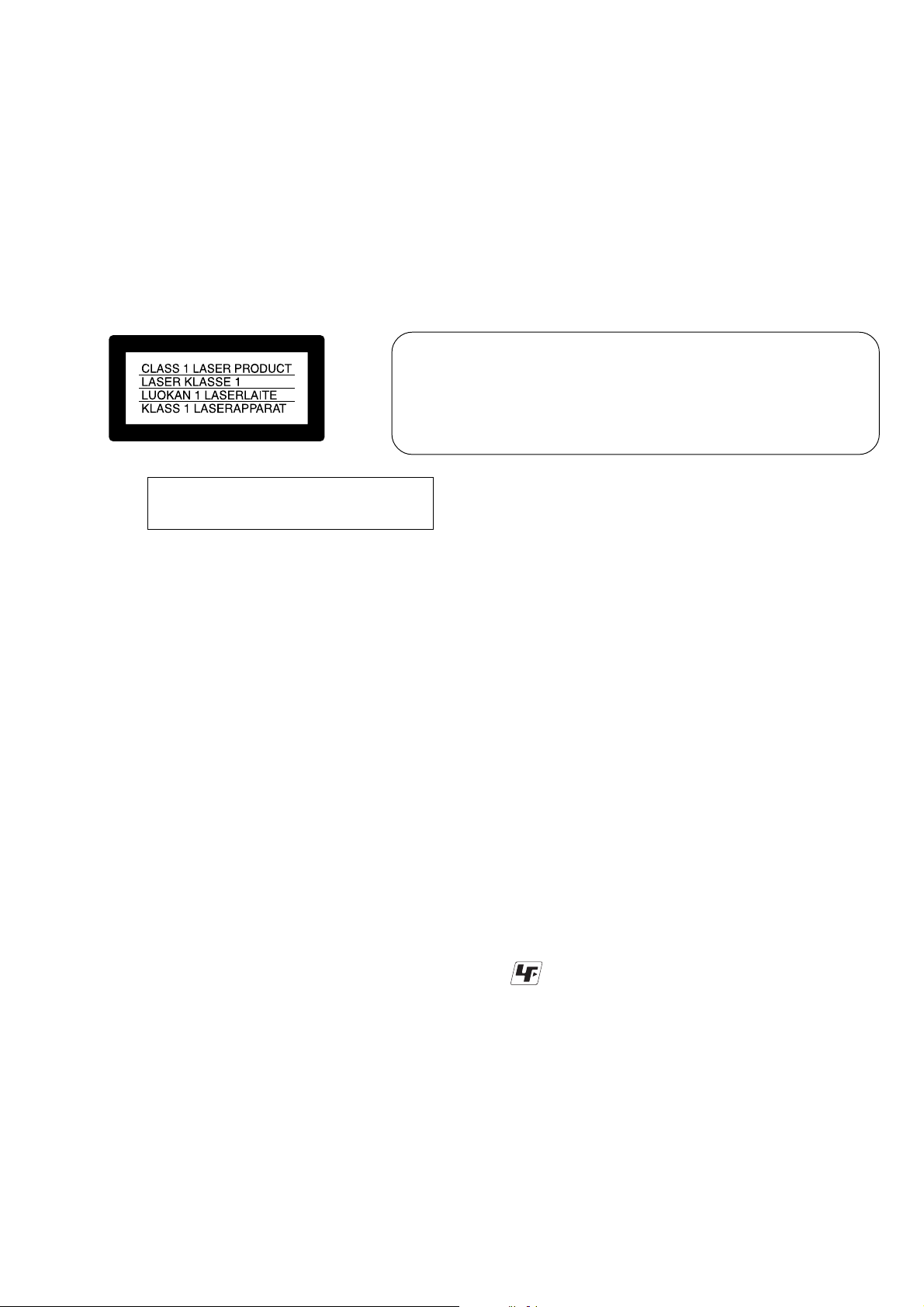
Unleaded solder
Boards requiring use of unleaded solder are printed with the leadfree mark (LF) indicating the solder contains no lead.
(Caution: Some printed circuit boards may not come printed with
the lead free mark due to their particular size.)
: LEAD FREE MARK
Unleaded solder has the following characteristics.
• Unleaded solder melts at a temperature about 40°C higher than
ordinary solder.
Ordinary soldering irons can be used but the iron tip has to be
applied to the solder joint for a slightly longer time.
Soldering irons using a temperature regulator should be set to
about 350°C.
Caution: The printed pattern (copper foil) may peel away if the
heated tip is applied for too long, so be careful!
• Strong viscosity
Unleaded solder is more viscous (sticky, less prone to flow) than
ordinary solder so use caution not to let solder bridges occur such
as on IC pins, etc.
• Usable with ordinary solder
It is best to use only unleaded solder but unleaded solder may
also be added to ordinary solder.
— 3 —
Page 4

TABLE OF CONTENTS
Section Title Page
Section Title Page
1. SERVICE NOTE
1-1. Note for Repair ································································1-1
1-2. Discharging of the Charging Capacitor (C205)···············1-1
1-3. Note in Lens Frame Installation ······································ 1-2
1-4. Notes on Handling the Laser Diode
[Laser Unit (D109) on the AF-008 FLEXIBLE
BOARD]··········································································1-2
1-5. Description on Self-diagnosis Display ····························1-3
2. DISASSEMBLY
2-1. Disassembly·····································································2-1
2-2. Service Position ·······························································2-5
2-3. The Method of Attachment of Harnesses························2-7
2-4. Circuit Boards Location ··················································2-8
3. BLOCK DIAGRAMS
3-1. Overall Block Diagram (1/3)···········································3-1
3-2. Overall Block Diagram (2/3)···········································3-3
3-3. Overall Block Diagram (3/3)···········································3-5
3-4. Power Block Diagram (1/2)·············································3-7
3-5. Power Block Diagram (2/2)·············································3-9
4. PRINTED WIRING BOARDS AND
SCHEMATIC DIAGRAMS
4-1. Frame Schematic Diagrams·············································4-1
Frame Schematic Diagram (1/2) ·····································4-1
Frame Schematic Diagram (2/2) ·····································4-3
4-2. Schematic Diagrams························································ 4-5
CD-515 FLEXIBLE (CCD IMAGER) ···························4-7
ST-111 (FLASH DRIVE) ·············································4-35
FL-147 (FLASH UNIT) ···············································4-36
PL-001 FLEXIBLE (PLUNGER) ································4-36
CF-099 (CF/MS CONNECTOR) ·································4-37
BB-005 FLEXIBLE
(SY-DD EXTENSITON BOARD) ·······························4-39
MS-211 FLEXIBLE
(SY-CF EXTENSION BOARD) ··································4-41
JK-269 FLEXIBLE (USB, A/V JACK) ························4-43
AF-008 FLEXIBLE (AF LASER)································4-45
RE-003 FLEXIBLE (SHUTTER SWITCH) ················4-45
BT-026 FLEXIBLE (BATTERY IN)····························4-46
LI-072 FLEXIBLE
(LITHIUM BATTERY) ···············································4-46
CONTROL SWITCH BLOCK
(SW51610) (REAR SW) ··············································4-47
CONTROL SWITCH BLOCK
(SW51610) (MODE SW) ············································4-49
4-3. Printed Wiring Boards ···················································4-51
CD-515 FLEXIBLE······················································4-53
ST-111 ···········································································4-61
FL-147 ··········································································4-61
PL-001 FLEXIBLE ······················································4-62
CF-099 ··········································································4-63
BB-005 FLEXIBLE ······················································4-63
MS-211 FLEXIBLE ·····················································4-64
JK-269 FLEXIBLE·······················································4-65
AF-008 FLEXIBLE ······················································4-66
BT-026 FLEXIBLE ······················································4-66
RE-003 FLEXIBLE ······················································4-66
LI-072 FLEXIBLE ·······················································4-66
4-5. Mounted Parts Location ················································4-71
5. REPAIR PARTS LIST
5-1. Exploded Views·······························································5-2
5-1-1.Main Block ······································································5-2
5-1-2.Cabinet (Front) Block······················································5-3
5-1-3.Grip Block ·······································································5-4
5-1-4.Lens Block·······································································5-5
5-1-5.Cabinet (Upper) Block ····················································5-6
5-1-6.Cabinet (Rear) Block·······················································5-7
5-2. Electrical Parts List ·························································5-8
DSC-V3
— 4 —
Page 5

1-1. NOTE FOR REPAIR
When installing a connector, don’t press down at wire of connector.
It is possible that a wire is snapped.
1. SERVICE NOTE
Make sure that the flat cable and flexible board are not cracked of
bent at the terminal.
Do not insert the cable insufficiently nor crookedly.
Cut and remove the part of gilt
which comes off at the point.
(Be careful or some
pieces of gilt may be left inside)
When remove a connector, don’t pull at wire of connector.
It is possible that a wire is snapped.
1-2. DISCHARGING OF THE
CHARGING CAPACITOR (C205)
The charging capacitor (C205) is charged up to the maximum 300
V potential.
There is a danger of electric shock by this high voltage when the
capacitor is handled by hand. The electric shock is caused by the
charged voltage which is kept without discharging when the main
power of the unit is simply turned off. Therefore, the remaining
voltage must be discharged as described below.
Preparing the Short Jig
To preparing the short jig, a small clip is attached to each end of a
resistor of 1 kΩ /1 W (1-215-869-11).
Wrap insulating tape fully around the leads of the resistor to prevent
electrical shock.
1 kΩ/1 W
Wrap insulating tape.
Discharging the Capacitor
Short-circuit between the positive and the negative terminals of
charged capacitor with the short jig about 10 seconds.
R:1 kΩ/1 W
(Part code:
1-215-869-11)
DSC-V3
1-1
Page 6

1-3. NOTE IN LENS FRAME
INSTALLATION
When tightening a screw , have both sides of the lens b lock assemb ly
so as not for the load to depend.
Lens flame
Lens block assembly
M1.7
M1.7
ST ground plate
1-4. NOTES ON HANDLING THE LASER DIODE
[LASER UNIT (D109) ON THE AF-008 FLEXIBLE BOARD]
The laser diode may suffer electrostatic breakdown because of the
potential difference generated by the charged electrostatic load, etc.
on clothing and the human body.
During repair, pay attention to electrostatic breakdown and also use
the procedure in the printed matter which is included in the repair
parts.
The flexible board is easily damaged and should be handled with
care.
Note: Adjustment is needed when laser unit (D109) on the AF-
008 flexible board is replaced.
Refer to “CAMERA adjustmen 5” and “CAMERA
adjustment 6” of SERVICE MANUAL, ADJ (9-876-762-
51.pdf).
Laser unit
(D109)
DSC-V3
1-2
Page 7
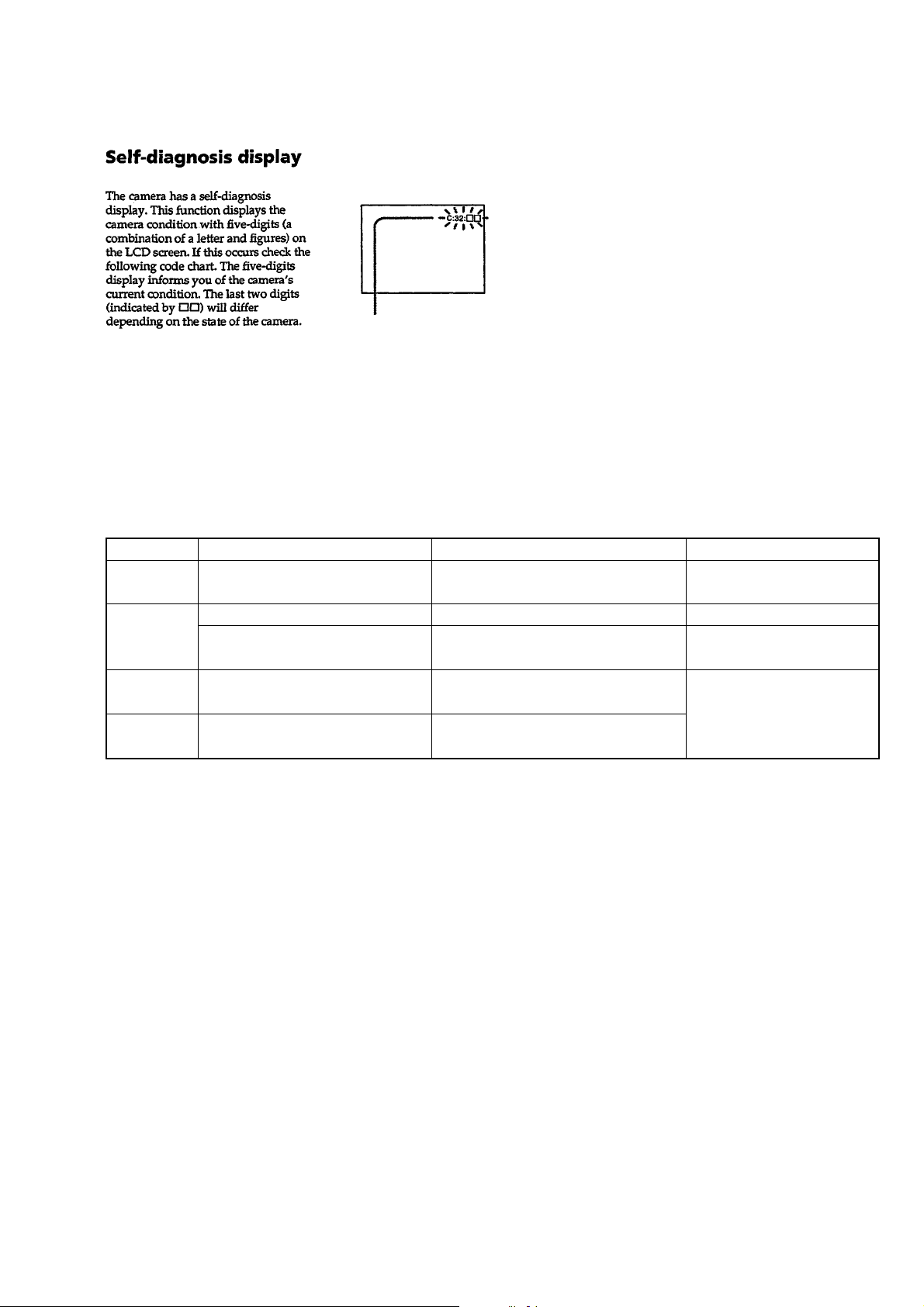
1-5. DESCRIPTION ON SELF-DIAGNOSIS DISPLAY
Self-diagnosis display
• C: ss: ss
You can reverse the camera
malfunction yourself. (However,
contact your Sony dealer or local
authorized Sony service facility
when you cannot recover from the
camera malfunction.)
• E: ss: ss
Contact your Sony dealer or local
authorized Sony service facility.
Display Code
C:32:ss
C:13:ss
E:61:ss
E:91:ss
Countermeasure
Turn the power off and on again.
Format the recording medium.
Insert a new recording medium.
Checking of lens drive circuit.
Checking of flash unit or replacement
of flash unit.
Cause
Trouble with hardware.
Unformatted recording medium is inserted.
Recording medium is broken.
When failed in the focus and zoom
initialization.
Abnormality when flash is being
charged.
Caution Display During Error
SYSTEM ERROR
FORMAT ERROR
MEMORY STICK ERROR,
CF CARD ERROR
—
DSC-V3
1-3E
Page 8

Link
Link
2. DISASSEMBLY
DISASSEMBLY
DISASSEMBLY
THE METHOD OF ATTACHMENT OF HARNESSES
THE METHOD OF ATTACHMENT OF HARNESSES
CIRCUIT BOARDS LOCATION
CIRCUIT BOARDS LOCATION
SERVICE POSITION
SERVICE POSITION
HELP
HELP
DSC-V3
Page 9
2. DISASSEMBLY
The following flow chart shows the disassembly procedure.
2. DISASSEMBLY
2. DISASSEMBLY
HELP
HELP
2-1. DISASSEMBLY
Don't disconnect
the FP-082 flexible board
from the connector on
the SY-106 board even after
the cabinet (upper) block
was removed.
6
3
1
1
1
2
5
4
1 P2 torasuta screw (M1.7)
2 Claw
x1
x4
3 Lifting up the cabinet (upper) block.
4 FP-082 flexible board: CN006
5 Capacitor cover
x1
6 Cabinet (upper) block
Note: High-voltage cautions
Discharging the Capacitor
Short-circuit between the two
points with the short jig about 10
seconds.
R:1 kΩ/1 W
(Part code:
1-215-869-11)
4
3
5
3
The battery lid
can't be disassembled.
When replacing the battery lid,
cut the lid with nippers
to break and replace it.
Battery lid
1
7
2
4
1
1 P2 torasuta screw (M1.7)
2 Cabinet bottom
x1
3 Open the battery lid.
4 P2 lock ace screw (M1.7)
5 Claw
6 Flexible board
x1
x3: CN702, 703, 801
7 Cabinet (rear) block
6
1
to Page 2-3
x5
x1
4
1
0
9
3
5
1
6
4
7
8
2
HELP
1 Tape (A)
x2
2 Flexible board x2: CN004, 007
x1
: CN003
x1
x1
: CN005
3 P2 screw (M1.7)
2
4 Lifting up the ST-111 board.
5 Connector
6 Flexible board
7 ST-111board
8 P2 screw (M1.7)
x2
9 P2 tapping screw (M1.7)
0 Flash unit
x1
3
3
6
5
1
1 Harness cover
2 ST blind
3 Claw
x1
x4
4 ST cover assy
5 Sheet
x1
6 FL-147 board block
x1
x1
2
When you disassemble
the FL-147 board
(harness (HN-001, HN-002)),
assemble with refer to page 2-7
" The method of attachment
of Harnesses ".
3
2
1
1 SY protection sheet
2 P2 tapping screw (M1.7)
3 Control switch block
4 Claw
x1
5 LCD block
5
x1
HELP
x5
DSC-V3
2-1 2-2
Page 10

from Page 2-2
4
1
4
3
1 Flexible board x1: CN752
2 Connector
3 Connector
4 Claw
5 Lens block
x2
x1
x2
: CN701, 704
: CN401
5
2
2. DISASSEMBLY
2. DISASSEMBLY
1
2
1 P2 tapping screw (M1.7)
2 P2 torasuta screw (M1.7)
3 Grip block
x3
x1
3
1
1
1
1 P2 tapping screw (M1.7)
2 JK-269 flexible board
2
2
x3
HELP
HELP
1
1
1 Flexible board
2 P2 tapping screw (M1.7)
3 SY-106 board
x3
: CN201, 451, 763
x1
3
2
qd
qf
1 Claw
2 Grip assy
3 Connector x
4 P2 tapping screw (M1.7)
5 Connector x2: CN083, 085
6 DD-217 board
7 Claw
8 LI-072 flexible board
9 Claw
0 BT-026 flexible board
qa Claw
qs RE-003 flexible board
qd Screw (M1.7)
qf CF-099 board
x1
x2
x1
x1
qs
1
1
: CN001
x2
qa
7
0
8
9
5
5
3
4
6
x2
When removing the grip assy,
detents are firmly engaged
and therefore take care not to
get injured with projection, etc.
DSC-V3
2-3 2-4
Page 11
2-2. SERVICE POSITION
6
3
1
2
2. DISASSEMBLY
2. DISASSEMBLY
Cabinet (rear) block
5
1
7
2
1
4
5
1
6
1
qd
qf
qs
1
qa
1
7
8
2
9
5
5
0
6
3
4
Lens block
It is connection needlessness
at the time of a play mode check.
JK-269
flexible board
SY-106 board
AC power
adaptor
DD-217 board
BB-005
flexible board
Cabinet (upper) block
AC IN
4
1
3
4
3
4
1
2
5
1
2
1
1
2
1
Color monitor
3
1
2
3
DSC-V3
2-5 2-6
Page 12

2. DISASSEMBLY
SY
-106
2. DISASSEMBLY
2-3. THE METHOD OF ATTACHMENT OF HARNESSES
Cut the both ends of the harness at position shown below
to expose the copper leads.
2.3mm2.3mm
Harness (HN-001) 1-963-220-XX
FL-147 board
Blue
Pink
ST-111 board
Cut the both ends of the harness at position shown below
to expose the copper leads.
White
10mm2.3mm
Black
White
When connecting the harness to
the strobe capacitor terminals,
wind the naked leads of the harness
around the terminals by more than
2.5 turns, and then solder them.
Capacitor
Harness
2-4. CIRCUIT BOARDS LOCATION
BT-026 flexible
RE-003 flexible
CF-099
BB-005 flexible
LI-072 flexible
DD-217
CD-515 flexible
MS-211 flexible
PL-001 flexible
SY
-106
FL-147
ST-111
AF-008
CH-146
(included in SY-106)
SY-106
(including CH-146)
JK-269 flexible
Harness (HN-002) 1-963-221-XX
Board Name Function
AF-008 FLEXIBLE AF LASER
BB-005 FLEXIBLE SY-DD EXTENSION BOARD
BT-026 FLEXIBLE BATTERY IN
CD-515 FLEXIBLE CCD IMAGER
CF-099 CF/MS CONNECTOR
CH-146 CCD SIGNAL PROCESS
(included in SY-106)
DD-217 FRONT CONTROL, DC IN, DC/DC CONVERTER
FL-147 FLASH UNIT
JK-269 FLEXIBLE USB, A/V JACK
LI-072 FLEXIBLE LITHIUM BATTERY
MS-211 FLEXIBLE SY-CF EXTENSION BOARD
PL-001 FLEXIBLE PLUNGER
RE-003 FLEXIBLE SHUTTER SWITCH
ST-111 FLASH DRIVE
SY-106 CAMERA MODULE, CAMERA DSP, LENS DRIVE,
(Including CH-146) SH DSP, CF INTERFACE, LCD DRIVE, AUDIO,
LANC DRIVE, AF LASER/IR LED DRIVE, FLASH
CONTROL
DSC-V3
2-7 2-8E
Page 13

HELP
Sheet attachment positions and procedures of processing the flexible boards/harnesses are shown.
Tape (A)
Control switch block
(SW51610) (Mode Sw)
Harness
ST-111 board
Tape (A)
Control switch block
(SW51610) (Rear Sw)
DSC-V3
SY protection sheet
HELP
Page 14

3. BLOCK DIAGRAMS
Link
Link
POWER BLOCK DIAGRAM (1/2)OVERALL BLOCK DIAGRAM (1/3)
POWER BLOCK DIAGRAM (1/2)OVERALL BLOCK DIAGRAM (1/3)
OVERALL BLOCK DIAGRAM (2/3) POWER BLOCK DIAGRAM (2/2)
OVERALL BLOCK DIAGRAM (2/3) POWER BLOCK DIAGRAM (2/2)
OVERALL BLOCK DIAGRAM (3/3)
OVERALL BLOCK DIAGRAM (2/3)
DSC-V3
Page 15
3. BLOCK DIAGRAMS
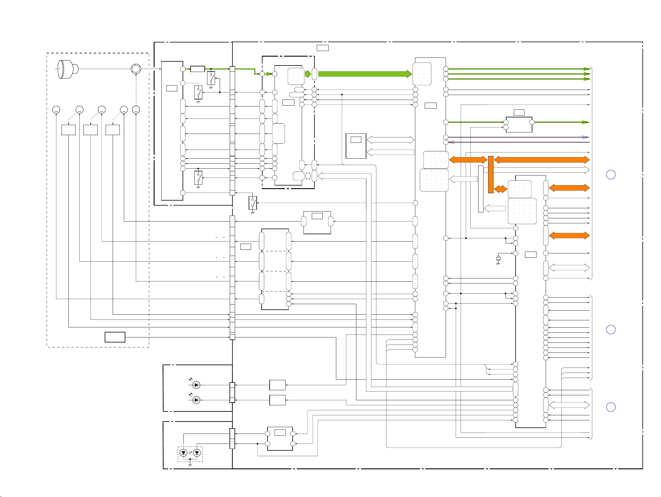
3-1. OVERALL BLOCK DIAGRAM (1/3)
LENS BLOCK
LENS
ZOOM
SENSOR
ZOOM
MOTOR
M
FOCUS
SENSOR
SHUTTER
MOTOR
M
A : VIDEO SIGNAL
A : AUDIO SIGNAL
A : VIDEO/AUDIO SIGNAL
FOCUS
MOTOR
M
IR FILTER
MOTOR
IR
SENSOR
LENS TEMP
SENSOR
IRIS
(METER)
IRIS
MOTOR
M
M
CD-515 FLEXIBLE BOARD
IC101
IMAGER
JK-269 FLEXIBLE BOARD (1/3)
(IR EMITTER)
(SELF TIMER)
AF-008 FLEXIBLE BOARD
05
( ) : Number in parenthesis ( ) indicates the division number of schematic diagram where the component is located.
CCD
D203
D204
SY-106 BOARD (1/3)
Q102
15
BUFFER
Q105
16
Q104
20
21
22
25
26
3
7
ı
14
1
5
6
4
2
23
Q103
24
RG, H1B, H2B
H1A, H2A
V2, V4, V5A, V5B,
V6, V7, V8, V9, V10
V1, V3A, V3B
VHLD
VST
VSUB
RANDOM
TRIG
VSUB CONT
IR FILTER±
FOCUS A, A, B, B
ZOOM A, A, B, B
IRIS A, A, B, B
SHUTTER±
IR SENS RST
F RST SENS
Z RST SENS1, 2
TEMP OUT LENS TEMP
IR LED K
SELF TIMER LED
D109
(LASER UNIT)
CN201
CCD OUT
14
POW SAVE
11
5
7
8
3
2
34
30
ı
23
36
32
31
33
35
21
17
19
Q201
CN451
1
ı
4
12
ı
19
IC451
LENS DRIVE
(3/9)
32
ı
39
24
ı
27
20
ı
23
6
8
28
29
10
CN752
(1/3)
2
4
CN763
LD
6
7
PD
10
11
CH-146 BOARD
86
6
133
37
33
5
42
2
51
4
37
1
48
3
9
113 109
12
112 115
ı
125 119
18
118 121 7
20
10
7
20
11
17
10
11
19
13
8
19
21
135
36
A6
FOCUS
B5
MOTOR
A4
DRIVER
B4
C1
ZOOM
D2
MOTOR
E1
DRIVER
E2
G4
IRIS
H4
MOTOR
G5
DRIVER
H6
SHUTTER
E7
MOTOR
D7
DRIVER
Q601
IR LED
DRIVE
Q502 (1/2)
LED
DRIVE
IC601
5
AF LASER
DRIVE
1
(9/9)
134 136
6 9 12 15
18 21 24
27 30 32
66
IC101
CCD SIGNAL
PROCESSOR,
TIMING
GENERATOR
B8
C8
C7
B7
B3
B2
A2
A1
G1
H2
G2
G3
F7
F8
H8
2
4
49
101 120
3
126
2 4
–
105
132
124
123
129
84
99
CP201
CAMERA
MODULE
(1/9)
22
ı
35
45
46
47
48
XFE CS, XTG CS
38
39
40
ı
CAM SO, XCAM SCK, XCAM RST
42
VSUB CONT_IC_302
IC452
7
IR FILTER
6
MOTOR DRIVE
HR EN2, HR DIR2A, HR DIR2B
HR EN0, HR DIR0A, HR DIR0B
HR EN3, HR DIR3A, HR DIR3B
2
3
(3/9)
MSHUT EN
MSHUT DIR
MSHUT REF
XIR RST SENS
XFC RST SENS
XZM RST SENS1, 2
CA AD00 – CA AD13
CA HD
CAM F
TG CLK
MCKTG
IC303
CAM F
512M
SDRAM
(2/9)
IR FILTER IN,
IR FILTER EN (OUT)
DQ0 – 31, DQM0 – 3
AQ0 – 12, BA0,1
CAM SO, XCAM SCK, XCAM RST
IR LED ON
GEN STRB ON
EXT STRB ON
STRB ON
AA10 AC10 Y10
AB10 AC9 AA8
Y8 Y9
AB9
AA7 AA9
AB8 AA6
AC6
Y6
AC3
AC7
CAMERA DSP
AB21
AA3
Y3
L2
L3
M2
J3
K4
J2
M4
N3
M3
AC20
U4
Y2
F2
F3
G3
R4
AC21
AA20
AB20
D1
Y7
V22 U20 U21 W22
V20 Y22 V21 W20
W21 Y20 Y21 Y19
K21 L22 L20 M22 L21
M23 M20 N22 M21 N23
N21 P22 N20 P20 R23
R22 P21 T23 R20 U23
R21 T22 T20 U22 T21
C1
D2
D6
C6
IC302
(2/9)
E1
AC13
AB14
AA22 AB23 AB22 AA21
P1
J20
J22
P4
D7
AA11
MC D0 - D15
MC A1 - A25
ADDRESS BUS MC A0 - A25
MC A0 - A25
VIDEO AMP ON
MC CKIO
X501
27MHz
MC XCS IC 302REG
MC XCS IC 302SDRAM
XSYS RST
SYS V
CAM SO, XCAM SCK, XCAM RST
SELF TIMER LED
PRELAMP AF CONT
PRELAMP AF ON
IC301
VIDEO AMP
(2/9)
1
MC D0 - D15
L21 L23 M24 K23
J21 J22 F24
PD LEV
H22
H21 M23 K22
K21
L24 F23 E23
G21
V22 V21 V23 R22 W22
W21 T22 R23 N21
U22
P21 P23 R21 M22
P22
P24 U21 U23 N22
T21
N23 T24 M21 T23
U24
D21
A7
H1
A6
A17
C18
D14
K2
AA8
AC12
AA9
AC16
A2
A12
B12
C23
G2
H23
F1
AC14
D5
DATA BUS MC D0 - D15
CAM F
XFE CS
XTG CS
LENS TEMP
MSHUT REF
B21
MC CAM,
24
IC501
SH DSP,
FLASH
(4/9)
PANEL R
PANEL G
PANEL B
HDO
PANEL V
XSYS RST
V OUT
AU AIN
AU AOUT
MC CKIO
MC D0 - D15
MC A0 - A10, A24
MC MSDIO,
MC MSBS,
MC MSSCLK
B16
B15
D16
XACCESS LED
C22
XAU LINE MUTE
AA18
D22
AB7
AD14
J1
K1
L1
M1
B17
A11
B11
C11
AD16
L22
AD20
AB15
AA7
AA5
AC13
AA17
AA14
AA6
AC19
AB11
AD19
AC15
AB5
AB13
B13
D13
C13
AD11
D11
AU SEN
MELODY ENV
MELODY
USBPHY D±
MC XCS IC 582
SYS SI, SYS SO, XSYS SCK
XPANEL TG CS
AE LOCK LED
XPROGRAM DIAL A, B
PROGRAM DIAL OSABORI
XASHOE JACK IN
EXT STRB CONT
XSTB POPUP
STB PLUNGER
XSTRB PWR SAVE
STRB CHRG
XSTRB FULL
GEN STRB ON
EXT STRB ON
XAE LOCK ON
FR SI, FR SO, XFR SCK
TALLY LED
STRB ON
XSHTR ON
FR INT
XCS MC
XSYS RST
SYS V
1
OVERALL (2/3)
(PAGE 3-3)
2
OVERALL (3/3)
(PAGE 3-6)
3
OVERALL (3/3)
(PAGE 3-5)
DSC-V3
3-1 3-2
Page 16

3-2. OVERALL BLOCK DIAGRAM (2/3) ( ) : Number in parenthesis ( ) indicates the division number of schematic diagram where the component is located.
SY-106 BOARD (2/3)
1
OVERALL (1/3)
(PAGE 3-2)
SYS SI, SYS SO, XSYS SCKSYS SI, SYS SO, XSYS SCK
XPANEL TG CS
PANEL R
PANEL G
PANEL B
HDO
PANEL V
XSYS RST
BL LEV
D11
E11
F11
A2
B1
C1
A5
B4
A4
B5
G10
IC801
LCD DRIVE
(6/9)
E1 F1 G1
H2 H1 J2
J1 K1 K3
L3 K4
H11 L10
L6
L7
L8
J11
RGT, HCK1, HCK2,
HST, PCG, XSTBY,
DWN, EN,
VCK, WIDE, REF, VP
CF D0 - D15
CF A0 - A10
PANEL R
PANEL G
PANEL B
HDO
PANEL V
XSYS RST
XPANEL TG CS
MC CKIO
XSYS RST
MC XCS IC 582
MC D0 - D15
MC A0 - A10, A24
MC MSDIO, MC M BS, MC MSSCLK MC MSDIO, MC M BS, MC MSSCLK
C7
A11
CF INTERFACE
C5
H10 J10 J11 J12
K8 K11 K12 L7
L8 L10 L12 M8
M9 M10 M11 M12
B9
D12 E10
E11 E12 F10
F11 F12 G10
G11 G12 H11
IC582
(5/9)
A1 A2 A3 A4
B1 B3 B4 C1
C2 D1 D2 D3
E2 E3 F2 F3
F1 G1 G2
G3 H1 J1
J2 K1 K2
L1 L2
M7
CN801
VR
VG
VB
COM
VST PANEL
CN702
BL H
BL L
4
5
3
23
24
2
6
ı
,
9
11
ı
14
19
ı
22
4
6
MS-211 FLEXIBLE BOARD
CN001CN704
3
19
5
22
7
29
9
31
11
34
13
49
15
50
17
52
25
33
27
41
30
44
ı
32
48
1 54
MC MSDIO, MC M BS,
8
4
16
12
56
XACCESSS LEDXACCESSS LED
PANEL UNIT
MONITOR
BACKLIGHT
CF D0 - D15
CF A0 - A10
RESET
XCD1, 2
MC MSSCLK
XMS IN
LCD901
COLOR
LCD
D901
CF-099 BOARD
CN101CN002
3
19
5
22
7
29
9
31
11
34
13
49
15
50
17
52
25
33
27
41
30
44
ı
32
48
5151
1 54
8
4
16
12 6
56
CF D0 - D15
CF A0 - A10
CF RESET
XCD1, 2
MC MSDIO, MC M BS, MC MSSCLK
XMS IN
Q101
LED
DRIVE
D105
(ACCESS)
CN105
CN104
2
ı
6
21
ı
23
8
10
ı
12
41
26 25
27
ı
31
47
ı
48
14
ı
20
4
2
8
CF CARD
COMPACT FLASH
TYPE I
MEMORY
STICK
MIC901
MICROPHONE
ST-111 BOARD (1/2)
CN003
1
05
USBPHY D± USBPHY D±
USB JACK IN
V OUT
V OUT
AU OUT
AU AIN
AU AOUT
XAU LINE MUTE
AU SEN
MELODY ENV
MELODY
CN006
(1/2)
MIC SIG
1 45
Q502 (2/2)
MODULATOR
CN751
(1/2)
SYS SO, XSYS SCK
BEEP
MIC IN
H6
H7
H2
H3
G4
H4
C1
A7
IC401
AUDIO AMP
(7/9)
F1
A2
A4
XAV JACK IN
Q702
XUSB JACK IN
XRST SW
XMS IN
XCD1, 2
IC701
1 2 4
(8/9)
XU DRIVE IN
BL L
BL H
BL LEV
XAV JACK IN
4
OVERALL (3/3)
(PAGE 3-5)
SP ±
60
CN752
JK-269 FLEXIBLE BOARD (2/3)
(2/3)
17
USB D±
15
USB JACK IN
12
V OUT
23
AU OUT
21
XAV JACK IN
25
CN401
1
2
A : VIDEO SIGNAL
A : AUDIO SIGNAL
A : VIDEO/AUDIO SIGNAL
XRESET FR
SP901
SPEAKER
60
CN101
VCC
S101
RESET
3
2
1
(USB)
J003
A/V OUT
(MONO)
DSC-V3
3-3 3-4
Page 17
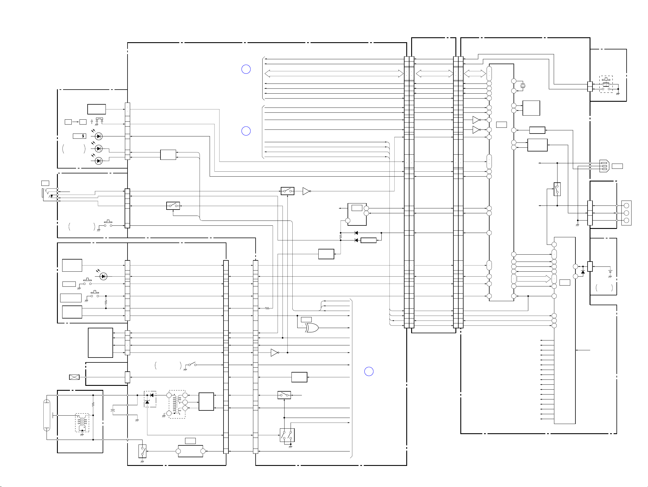
3-3. OVERALL BLOCK DIAGRAM (3/3)( ) : Number in parenthesis ( ) indicates the division number of schematic diagram where the component is located.
J102
ACC
FLASH
UNIT
CONTROL SWITCH BLOCK
(SW51610) (REAR SW)
S001 – 005,
007 – 015
MS
D106
SELF TIMER/
RECORDING
D107
(AE/AF LOCK)
S016
CHG/
D108
CF
FUNCTION
KEY
JK-269 FLEXIBLE BOARD (3/3)
LANC DC
S101
LENS ADAPTOR
DETECT
XLANC JACK IN
LANC SIG
ACC STRB ON
CONTROL SWITCH BLOCK
(SW51610) (MODE SW)
S104
MODE DIAL
S103
POWER
S105
NIGHTFRAMING
/NIGHTSHOT
S106
JOG DIAL
PLUNGER
XE_H
TRIGGER
XE_L
EXECUTE
DIAL A, B
L201
(POWER)
ADVANCED
ACCESSORY
SHOE
PL-001 FLEXIBLE
BOARD
CHARGING
CAPACITOR
FL-147 BOARD
D110
+
C205
SY-106 BOARD (3/3)
CN703
11
KEY AD0 – 2
2
9
KEY AD4
10
XCHARGE LED
5
8
AE LOCK LED
6
CN752
(3/3)
XLANC JACK IN
6
LANC SIG
8
ACC STRB ON
10
KEY AD3C
27
ST-111 BOARD (2/2)
CN005
MODE DIAL0, 1
4
3
PWR LED ON
6
XPWR ON
10
KEY AD3
2
KEY AD3C
12
Program Dial A, B
14
13
CN004
LANC SIG
1
INTE STRB ON
7
HOT
4
5
LANC JACK IN2
8
CN007
4
ı
6
D202
Q203
Q504
LED
DRIVE
Q654
EXT STRB CONT
S201
STROBE
POP UP DETECT
T202
5 4
2
TALLY LEDXTALLY LED
AE LOCK LED
1
3
IC201
FLASH
2
CONTROL
Q201, 202
TRANS
DRIVE
4
CN006
(2/2)
BB-005 FLEXIBLE
BOARD
XAE LOCK ON
XSHTR ON
3
OVERALL (1/3)
(PAGE 3-2)
4
OVERALL (2/3)
(PAGE 3-4)
MODE DIAL0, 1
11
13
PWR LED ON
5
XPWR ON XPWR ON
9
KEY AD3
14
KEY AD3C
12
Program Dial A, B
3
4
LANC SIG
19
INTE STRB ON
16
HOT
17
LANC JACK IN2
15
XSTRB POPUP
43
STRB PLUNGER
ı
45
28
ST UNREG
ı
33
XSTRB PWRSAVE
26
STB FULL
22
STRB ON
25
FR INT
XCS MC
XSYS RST
SYS V
XAV JACK IN
XUSB JACK IN XUSB JACK IN
XU DRIVE IN XU DRIVE IN
XMS IN XMS IN
XRST SW
BL L
BL H
35
33
41
37
32
34
43
42
27
30
29
31
442
3
1
18
13
20
24
21
CN751
(2/2)
ı
ı
BL LEV
Q652, 653
KEY AD3C
Q651
Q753, 754
KEY AD0 – 2
KEY AD4
XCHARGE/XSTRB LED
Q703
LANC SIG
INTE SALA SIG
XPROGRAM DIAL A, B
IC751
(9/9)
1 2 4
Q751
PLUNGER
DRIVE
ST UNREG
Q752
LANC DC
Q655, 656
LANC SIG
SWITCH
EXT STRB CONT
TALLY LED
AE LOCK LED
PROGRAM DIAL
OSABORI
EXT STRB ON
GEN STRB ON
XASHOE JACK IN
XSTB POPUP
STB PLUNGER
XSTRB PWR SAVE
STRB CHRG
XSTRB FULL
STRB ON
11
D632
D631
FR SI, FR SO, XFR SCKFR SI, FR SO, XFR SCK
BL LEVEL
IC631
10
LANC OUT
12
LANC
DRIVE
(8/9)
Q631, 632
SWITCH
2
OVERALL (1/3)
(PAGE 3-2)
XRSTX
BL L
BL H
LANC IN
CN301CN701
48
48
50
50
46
46
72
72
56
56
67
67
74
74
5959
7070
6161
6464
6363
71
71
73
73
75
75
7979
5454
4040
42
42
5858
807880
78
6262
6969
7777
7676
3636
3030
3232
XAE LOCK ON
XSHTR ON
FR SI, FR SO, XFR SCK
FR INT
XCS MC
XSYS RST
SYS V
XAV JACK IN
XLANC JACK IN FR
KEY AD0 – 2
KEY AD4
XCHARGE/XSTRB LED
LANC IN
LANC OUT
XLANC PWR ON
MODE DIAL0, 1
XPWR LED ON
KEY AD3
XRSTX
BL L
BL H
BL LEVEL
DD-217 BOARD
CN084CN302
26262626
28282828
48
48
50
50
46
46
72
72
56
56
67
67
74
74
5959
7070
6161
6464
6363
71
71
73
73
75
75
7979
5454
4040
42
42
5858
807880
78
6262
6969
7777
7676
3636
3030
3232
Q104
Q103
D1
D2
E1
D9
E2
B3
B9
A3
C8
A6
B6
B4
J6
H6
G6
H7
B1
F3
F2
A8
J8
J9
B2
B8
J7
IC101
FRONT
CONTROL
(1/3)
XRST SW
J5
J4
J2
J3
A7
G1
G2
E8
H2
J1
A9
C1
D3
H1
D7
X101
32.768kHz
PLL
LOOP
FILTER
Q101, 102
BUFFER
Q106
BATTERY
CHARGE
DETECTOR
ACV UNREG
ST UNREG
BATT UNREG
SYS DD ON
FAST CHARGE
INIT CHARGE
BATT IN
DDCON SO, DDCON SCK
XCS DDCON
XRSTX
BL L
BL H
BL LEV
EVER 3.0V
PANEL 8.5V
A 3.1V
D 1.2V
BACK UP VCC
LANC 5.5V
SDRAM 2.8V
D 2.8V
A 2.8V
CAM –0.5V
CAM 15.5V
CAM –8.0V
CF 3.3V
PANEL 4.9V
M 5V
CAM 5V
ST 5V
Q011
CHG SW
E4
C7
D7
E3
D2
A7
L8
K8
K7
B7
G2
G1
B1
XAE LOCK ON
BATT/XEXT
BATT SIG
IC005
DC/DC
CONTROL,
RESET
(2/3)
CN085
XSHTR ON
CN001
CN083
D8
A10
RE-003
FLEXIBLE
BOARD
6
4
BT-026
FLEXIBLE
BOARD
1
BATT UNREG
ı
7
5
9
ı
16
LI-072
FLEXIBLE
BOARD
8
VL 3V
ı
11
ACV UNREG
S001
(SHUTTER)
BATT SIG
BATT GND
BT001
LITHIUM
BATTERY
J001
DC IN
TERMINAL
BT001
BATTERY
+
S
−
DSC-V3
05
3-5 3-6
Page 18
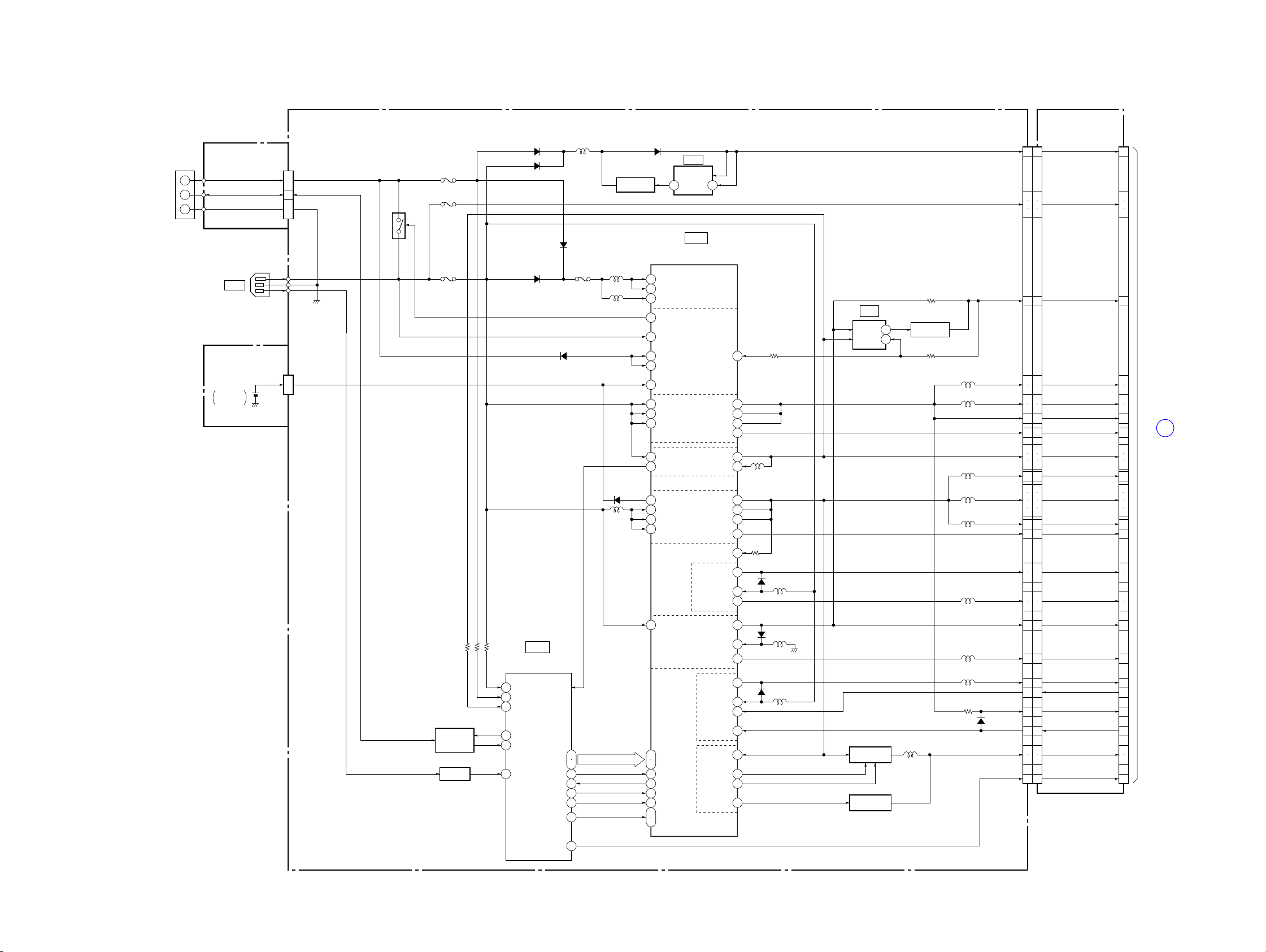
3-4. POWER BLOCK DIAGRAM (1/2)
( ) : Number in parenthesis ( ) indicates the division number of schematic diagram where the component is located.
BT001
BATTERY
TERMINAL
+
S
−
BT-026 FLEXIBLE
BOARD
BATT UNREG
BATT SIG
BATT GND
J001
DC IN
LI-072 FLEXIBLE
BOARD
BT001
LITHIUM
BATTERY
VL 3V
DD-217 BOARD
CN001
1
ı
7
8
9
ı
16
CN083
8
ı
11
ACV UNREG
BATT/XEXT
Q011
F003
F001
F002
Q106
BATTERY
CHARGE
DETECTOR
Q101, 102
BUFFER
D 1.2V
BATT UNREG
ACV UNREG
G8
H8 BATT SENS
F8 DD CON SENS
G1
G2
A7
D012
D011
D006
VL 3V
IC101
FRONT CONTROL
(1/3)
ACV SENS
BATT SO
BATT SI
BATT/XEXT
D002
L022, 023
D005
F004
BACK UP VCC
C1
D3
H1
A9
H2
J1
E8
SWITCHING
L001, 010
L027
D017
L005
DDCON SO,
DDCON SCK
XCS DDCON
BATT IN
FAST CHARGE
INIT CHARGE
SYS DD ON
Q002
D9
E9
B11
E4
D1
E5
D4
D8
G11
G10
G9
F9
B9
A10
J3
K1
J2
K5
L8
K8
K7
A7
E3
D2
C7
D7
D013
IC004
DC
CONTROL
15
(2/3)
IC005
DC/DC CONTROL, RESET
(2/3)
OUT8A
OUT8B
VCC8
CHG SW
VDCIN
MARK
BATT
VBCK
VCC1A
VCC1B
VCC1C
VCC2
VLDO2
VLDO3
OUT3A
OUT3B
OUT3C
VCC5
DIN
CLK
LD
CS
FCHG
ICHG
SYSDDON
USB PWR ON
VCH1A
VCH1B
VCH1C (FB4)
VLDO1
VCH3A (FB3)
VCH3B
VCH3C (FB6)
VCH3S
VCC GD
VLDO4
VLDO5
VOS72
VOS73
CBG
VCH2
OUT2
VCH4
OUT4
VCH5
OUT5
VCH6
OUT6
ICH6
REF6
VCC7
VCH7
ACV UNREG
B5
L10
K9
L9
A11
E11
F10
J1
H4
H3
H2
H1
J6
D009
K6
C8
J5
D008
L5
B8
G1
D007
F1
G2
B1
J4
K4
L3
K3
D 1.2V
L002
L006
L007
L003
IC003
DC
CONTROL
(2/3)
Q006, 009
SWITCHING
Q010
DC CONTROL
BB-005 FLEXIBLE
BOARD
LANC 5.5V
ST UNREG
CAM –0.5V
SWITCHING
L024
Q001
L011, 015
L017
L014
L013
L026
L019
L020
L012
D003
A 2.8V
D 2.8V
SDRAM 2.8V
EVER 3.0V
D 1.2V
PANEL 4.9V
M 5V
CAM 5V
ST 5V
CAM 15.5V
A 3.1V
CAM –8.0V
PANEL 8.5V
BL H
BL L
BL THH
BL LEV
CF 3.3V
1
4
CN302CN084
77
1
1
3
3
5
5
1111
313331
33
373937
39
25
27
29
49
51
53
55
19
23
45
SDRAM 2.8V
5757
99
25
27
29
PANEL 4.9V
4141
49
51
53
55
4747
3535
171917
212321
1313
PANEL 8.5V
1515
3030
3636
3434
3232
434543
XLANC IC ON
6363 63
LANC 5.5V
ST UNREG
CAM –0.5V
A 2.8V
D 2.8V
EVER 3.0V
D 1.2V
M 5V
CAM 5V
ST 5V
CAM 15V
A 3.1V
CAM –8.0V
BL H
BL L
BL THH
BL LEVEL
CF 3.3V
CN301
7
1
3
5
11
31
33
37
39
57
9
25
27
29
41
49
51
53
55
47
35
17
19
21
23
13
15
30
36
34
32
43
45
A
POWER 2
(PAGE 3-9)
DSC-V3
XLANC IC ON
A1
05
3-7 3-8
Page 19

3-5. POWER BLOCK DIAGRAM (2/2)
( ) : Number in parenthesis ( ) indicates the division number of schematic diagram where the component is located.
SY-106 BOARD
CN701
EVER 3.0V
9
1
ST UNREG
3
5
ST 5V
35
XLANC IC ON
63
LANC 5.5V
7
L751
M 5V
Q753, 754
STRB CHRG
Q755
CAM DD ON
Q751
STB PLUNGER
D 2.8V
IC701
OR GATE
(8/9)
Q633
IC631
LANC DRIVE
(8/9)
IC751
XOR GATE
(9/9)
14
FB751
CN751
CN703
EVER 3.0V
D 2.8V
CN752
IR LED A
D 2.8V
LANC DC
ST-111 BOARD
33
28
2422
45
43
CN006
739
ı
ı
EVER 3.0V
ST UNREG
13
ı
18
1
STRB PLUNGER
ı
3
ST 5V
CONTROL SWICHT BLOCK
(SW51610) (REEAR SW)
3
7
JK-269 FLEXIBLE BOARD
1
3
5
(IR EMITTER)
(SELF TIMER)
PANEL UNIT
T202
D108
CHG/
D106
SELF TIMER/
RECORDING
D107
(AE/AF LOCK)
D203
D204
CONTROL SWICHT BLOCK
(SW51610) (MODE SW)
CN005
8
IC201
FLASH CONTROL
J102
ACC
D110
(POWER)
CN007
FL-147 BOARD
PL-001 FLEXIBLE
BOARD
4
ı
6
FLASH
PLUNGER
UNIT
CP201
CAMERA
MODULE
IC201
3.3V
5
1
REG
(1/9)
4
(1/9)
L204
L203
L202
FB206
L205
FB203
FB204
CH-146 BOARD
52
57
71
53
54
55
56
50
51
49
IC101
CCD SIGNAL
PROCESSOR,
TIMING
GENERATOR
DSC-V3
A
POWER 2
(PAGE 3-8)
H11
G10
VIDEO AMP
CN801
18
11
CN702
IC502
1.8V
REG
4 1
(4/9)
IC301
(2/9)
1
4
6
VDD
REF
BL THH
BL H
BL L
CAM DD ON
STB PLUNGER
STRB CHRG
Q202, 203
D2.8V
A 3.1V
D 1.2V
L502
D 1.2V
AU 2.8V
M 5V
LCD901
COLOR
LCD
MONITOR
D901
BACKLIGHT
AD19
AC20
AC19
PU[6]
PU[2]
PU[0]
SDA(O/D)
IC501
MC CAM,
SH DSP,
FLASH
(4/9)
AD18
CAM 5V
CAM 15V
CAM –8.0V
D 2.8V
FB304
FB301
FB302
FB305
PI008
PI006
PI007
IC302
CAMERA
DSP
(2/9)
XIR SENS LED
U3
XZM RST LED
W2
XLENS RST LED
V4
FB581
L581
IC601
AF LASER
DRIVE
(9/9)
CF POWER ON
IC582
CF INTERFACE
(5/9)
Q452 (1/2)
L451
L452
L453
Q581
K6
Q451
LENS DRIVE
MOTOR DRIVE
L201
MS PWR ON
Q452 (2/2)
IC451
(3/9)
IC452
IR FILTER
(3/9)
CN201
10
38
CN704 CN001
35
CF VCC
37
39
MS VCC
18
58
CN451
5
9
31
CD-515 FLEXIBLE BOARD
CAM 15V
CAM –8.0V
35
CF VCC
37
39
MS-211
FB101
CN002 CN101
CCD IMAGER
35
35
37
37
39
39
CF-099 BOARD
FLEXIBLE
BOARD
MS VCC
18
MS PWR ON
58
IR SENS VCC
F RST VCC
Z RST VCC
18
18
58
58
ZOOM
IR
SENSOR
SENSOR
FOCUS
SENSOR
ZOOM
SENSOR
LENS BLOCK
IC101
Q102
L101
CN105
CN104
13
38
9
CF CARD
COMPACT FLASH
TYPE I
MEMORY
STICK
L401
L804
L813
IC802
2.8V
5 4
REG
(6/9)
IC401
AUDIO AMP
(7/9)
IC801
LCD DRIVE
(6/9)
L302
REF
EXTDA
PANEL 8.5V
15
PANEL 4.9V
41
BL LEVEL
32
BL THH
34
BL H
30
BL L
36
CAM 5V
47
CAM –0.5V CAM –0.5V
11
CAM 15V
17
19
CAM –8.0V
13
CF 3.3V CF 3.3V
43
45
D 2.8V
37
39
FB303
IC303
512M
SDRAM
(2/9)
SDRAM 2.8V
57
A 3.1V
21
23
25
D 1.2V
27
29
A 2.8V
31
33
49
M 5V
51
53
55
05
L304
A 2.8V
3-9 3-10E
Page 20

4-1. FRAME SCHEMATIC DIAGRAMS
1
3
4
FRAME SCHEMATIC DIAGRAM (1/2)
A
ADVANCED
ACCESSORY SHOE
4. PRINTED WIRING BOARDS AND SCHEMATIC DIAGRAMS
62
8
911127
10
13 14
15
165
CHARGING CAPACITOR
B
HARNESS (HN-002) x 2 HARNESS (HN-001) x 3
10
C
PL-001
FLEXIBLE
BOARD
D
(PLUNGER)
CN007
6
5
4
3
2
1
6P
STRB_PLUNGER
STRB_PLUNGER
STRB_PLUNGER
REG_GND
REG_GND
REG_GND
10P
CN004
SHOE_GND
SHOE_GND
N.C.
INTE_STRB_ON
LANC_JACK_IN2
123456789
N.C.
HOT
HOT
REG_GND
LANC_SIG
ST-111 BOARD
C205
CHARGING
CAPACITOR
(FLASH DRIVE)
CN003
2P
MIC_SIG
MIC901
E
MICROPHONE
F
AF-008
G
FLEXIBLE
BOARD
(AF LASER)
H
JK-269
FLEXIBLE
I
J
K
BOARD
(USB, A/V JACK)
(USB)
J102
ACC
J103
A/V OUT
(MONO)
GND
VCC
CN101
ID
D+
D-
1
MIC
REG_GND
2
45P
STRB_PLUNGER
CN006
45
STRB_PLUNGER
XSTRB_POPUP
STRB_PLUNGER
REG_GND
REG_GND
REG_GND
REG_GND
REG_GND
REG_GND
N.C.
ST_UNREG
ST_5V
STRB_ON
XSTRB_PWRSAVE
N.C.
REG_GND
REG_GND
LANC_SIG
REG_GND
STB_FULL
HOT
ST_UNREG
ST_UNREG
ST_UNREG
ST_UNREG
ST_UNREG
N.C.
N.C.
FP-082 FLEXIBLE
123456789
11PCN763
GND
1
GND
2
GND
3
N.C.
4
N.C.
5
LD
6
LD
7
N.C.
8
N.C.
9
PD
10
PD
11
CN752
27P
IR_LED_A
1
IR_LED_K
2
D2.8V
3
SELF_TIMER_LED
4
LANC_DC
5
XLANC_JACK_IN
6
REG_GND(N.C)
7
LANC_SIG
8
REG_GND(N.C)
9
ACC_STRB_ON
10
REG_GND
11
USB_JACK_IN
12
REG_GND
13
5
4
14
15
16
17
18
19
20
21
22
23
24
25
26
27
N.C
USB_D-
N.C
USB_D+
REG_GND
REG_GND
REG_GND(N.C)
A_OUT
REG_GND(N.C)
V_OUT
REG_GND
XAV_JACK_IN
REG_GND
KEY_AD3C
3
2
1
45P
CN751
STRB_PLUNGER
STRB_PLUNGER
STRB_PLUNGER
12PCN703
KEY_AD1
REG_GND
1234567
REG_GND
XSTRB_POPUP
EVER_3.0V
N.C.
XCHARGE_LED
1011121314151617181920212223242526272829303132333435363738394041424344
N.C.
REG_GND
REG_GND
REG_GND
REG_GND
REG_GND
N.C.
ST_UNREG
ST_UNREG
ST_UNREG
ST_UNREG
ST_UNREG
ST_UNREG
N.C.
XSTRB_PWRSAVE
STRB_ON
ST_5V
N.C.
STB_FULL
REG_GND
REG_GND
LANC_SIG
HOT
REG_GND
SY-106 BOARD (1/2)
(1/9) (CAMERA MODULE)
(2/9) (CAMERA DSP)
(3/9) (LENS DRIVE)
(4/9) (SH DSP)
(5/9) (CF INTERFACE)
(6/9) (LCD DRIVE)
(7/9) (AUDIO)
(8/9) (LANC DRIVE, DC SUPPLY)
(9/9) (AF LASER/IR LED DRIVE, FLASH CONTROL)
D_2.8V
AE_LOCK_LED
KEY_AD2
XTALLY_LED
9
8
KEY_AD0
KEY_AD4
101112
REG_GND
6P
N.C
BL_THH
CN702
12345
BL_THL
24P
N.C
BL_L
BL_H
6
CN801
VCK
CS
COM
VST
FL-147 BOARD
LANC_JACK_IN2
MODE_DIAL0
MODE_DIAL1
INTE_STRB_ON
KEY_AD3C
KEY_AD3
N.C.
1011121314151617181920212223242526272829303132333435363738394041424344
N.C.
KEY_AD3
KEY_AD3C
MODE_DIAL1
LANC_JACK_IN2
EN
DWN
MODE_DIAL0
VSSG
VDD
VSS
N.C.
INTE_STRB_ON
(FLASH UNIT)
XPWR_ON
N.C.
EVER_3.0V
PWR_LED_ON
N.C.
567
8
9
N.C.
N.C.
XPWR_ON
EVER_3.0V
PWR_LED_ON
PCG
HST
REF
SOUT(N.C)
XSTBY
101112131415161718192021222324
Program_Dial_B
4
Program_Dial_B
WIDE
HCK2
MIC_SIG
MIC_GND
Program_Dial_A
123
45
MIC_SIG
MIC_GND
Program_Dial_A
PSIG
HCK1
15P
CN005
N.C
1
KEY_AD3
2
MODE_DIAL1
3
MODE_DIAL0
4
N.C
PWR_LED_ON
EVER_3.0V
XPWR_ON
KEY_AD3C
Program_Dial_B
Program_Dial_A
REG_GND
5
6
N.C
7
8
N.C
9
10
N.C
11
12
13
14
15
(SW51610)(MODE SW)
CONTROL
SWITCH
BLOCK
CD-515 FLEXIBLE BOARD
(CCD IMAGER)
123456789
REG_GND
RG
H1A
H2A
REG_GND
39P
CN201
1011121314151617181920212223242526272829303132333435363738
H2B
REG_GND
H1B
CAM_15V
REG_GND
CCD_GND
POW_SAVE
CCD_GND
CCD_OUT
CCD_GND
CCD_GND
REG_GND
RANDOM_TRIG
REG_GND
VSUB_CONT
VSUB
REG_GND
V6
V8
V7
V9
V10
V5B
V5A
39
V4
V3B
V1
V2
VST
V3A
VHLD
REG_GND
REG_GND
CAM_-8.0V
CP201
CH-146
BOARD
CCD SIGNAL
PROCESS
39P
ZOOM_A
ZOOM_A
ZOOM_B
ZOOM_B
ZOOM_B
Z_RST_SENS2
Z_RST_SENS1
IRIS-A
ZOOM_A
ZOOM_A
TEST(N.C)
G
R
B
RGT
CN451
123456789
39
Z_RST_GND
Z_RST_VCC
ZOOM_B
IRIS-A
IRIS-B
IRIS-B
SHUTTER+
SHUTTER+
SHUTTER-
SHUTTER-
FOCUS_A
FOCUS_A
FOCUS_A
FOCUS_A
FOCUS_B
FOCUS_B
FOCUS_B
FOCUS_B
TEMP_GND
TEMP_OUT
1011121314151617181920212223242526272829303132333435363738
F_RST_SENS
F_RST_VCC
IR_SENS_RST
IR_SENS_GND
IR_FILTTER-
IR_SENS_VCC
IR_FILTTER+
IR_FILTTER-
IR_FILTTER+
123456789
CONTINUED ON
PAGE 4-3
DSC-V3
L
CONTROL
SWITCH
BLOCK
COLOR LCD MONITOR
LCD901
OVF
(SW51610)
M
(REAR SW)
D901 BACKLIGHT
LENS BLOCK
LENS
PANEL UNIT
05
4-1 4-2
FRAME (1/2)
Page 21

1
3 14114
6
897
122 10
13 2115
165 20
17
18
19
22
FRAME SCHEMATIC DIAGRAM (2/2)
A
B
C
D
E
F
SY-106 BOARD (2/2)
(1/9) (CAMERA MODULE)
(2/9) (CAMERA DSP)
G
CONTINUED ON
H
PAGE 4-2
I
J
K
L
M
(3/9) (LENS DRIVE)
(4/9) (SH DSP)
(5/9) (CF INTERFACE)
(6/9) (LCD DRIVE)
(7/9) (AUDIO)
(8/9) (LANC DRIVE, DC SUPPLY)
(9/9) (AF LASER/IR LED DRIVE, FLASH CONTROL)
CN704
VSS
2
MC_MSBS
4
MC_MSD1
6
MC_MSDIO
8
MC_MSD2
10
XMS_IN
12
MC_MSD3
14
MC_MSCLK
16
MS_VCC
18
VSS
20
D07
22
XCE1
24
XIORD
26
IREQ
28
A02
30
A00
32
D01
34
GND
36
GND
38
GND
40
XOE
42
A08
44
A07
46
A04
48
D08
50
D10
52
XCD2
54
XACCESS_LED
56
MS_PWR_ON
58
XRESET_FR
60
MODE_DIAL0
80
MODE_DIAL1
78
76
XRSTX
SYS_V
74
FR_INT
72
XUSB_JACK_IN
70
68
REG_GND
XLANC_JACK_IN_FR
66
XMS_IN
64
62
XPWR_LED_ON
MC_UPDATE
60
XLANC_PWR_ON
58
56
XCS_MC
XCHARGE/XSTRB_LED
54
REG_GND
52
50
FR_SO
FR_SI
48
46
XFR_SCK
44
REG_GND
LANC_OUT
42
LANC_IN
40
38
REG_GND
36
BL_L
34
BL_THH A_2.8V
32
BL_LEVEL
30
BL_H
XSHTR_ON
28
26
XAE_LOCK_ON
24
REG_GND
REG_GND
22
REG_GND
20
18
REG_GND
REG_GND
16
14
REG_GND
12
REG_GND
REG_GND
10
REG_GND
8
REG_GND
6
REG_GND
4
REG_GND
2
60P
80P
CN701
KEY_AD4
KEY_AD3
KEY_AD2
KEY_AD1
KEY_AD0
XPWR_ON
XSYS_RST
XLANC_IC_ON
XU_DRIVE_IN
XAV_JACK_IN
CAM_5V
PANEL_4.9V
CAM_15V
CAM_15V
PANEL_8.5V
CAM_-8.0V
CAM_-0.5V
EVER_3.0V
LANC_5.5V
ST_UNREG
ST_UNREG
ST_UNREG
CF_VCC
CF_VCC
CF_VCC
XIOIS16
CF_3.3V
CF_3.3V
XIOWR
XWAIT
D_2.8V
D_2.8V
A_2.8V
D_1.2V
D_1.2V
D_1.2V
A_3.1V
A_3.1V
50PCN105
50
GND
25
XCD2
D10
49
24
XIOIS16
48
D09
D02
2P
CN401
SP+
1
SP901
SPEAKER
SP-
2
XCD1
XCD1
1
1
D03
D03
3
3
D11
D11
5
5
D04
D04
7
7
D12
D12
9
9
D05
D05
11
11
D13
D13
13
13
D06
D06
15
15
D14
D14
17
17
D15
D15
19
19
XCE2
XCE2
21
21
XIOWR
23
23
A05
A05
25
25
A01
A01
27
27
D00
D00
29
29
D02
D02
31
31
A10
A10
33
33
CF_VCC
35
35
CF_VCC
37
37
CF_VCC
39
39
A09
A09
41
41
XWE
XWE
43
43
A06
A06
45
45
A03
A03
47
47
D09
D09
49
49
RESET
RESET
51
51
XWAIT
53
53
XREG
XREG
55
55
XIOIS16
57
57
GND
GND
59
59
79
79
KEY_AD4
77
77
KEY_AD3
KEY_AD2
75
75
73
KEY_AD1
73
71
71
KEY_AD0
69
69
XPWR_ON
67
67
XSYS_RST
N.C
65
65
N.C
63
63
XLANC_IC_ON
61
61
XU_DRIVE_IN
59
59
XAV_JACK_IN
57
57
M_5V
55
55
M_5V
M_5V
53
53
M_5V
M_5V
51
51
M_5V
M_5V
M_5V
49
49
47
CAM_5V
47
45
45
CF_3.3V
43
43
CF_3.3V
PANEL_4.9V
41
41
D_2.8V
39
39
37
37
ST_5V
ST_5V
35
35
33
33
A_2.8V
A_2.8V
31
31
D_1.2V
29
29
27
D_1.2V
27
25
D_1.2V
25
A_3.1V
23
23
A_3.1V
21
21
CAM_15V
19
19
17
17
CAM_15V
PANEL_8.5V
15
15
13
13
CAM_-8.0V
CAM_-0.5V
11
11
9
9
EVER_3.0V
LANC_5.5V
7
7
ST_UNREG
5
5
ST_UNREG
3
3
ST_UNREG
1
1
60PCN001
XACCESS_LED
MS_PWR_ON
80PCN301
MODE_DIAL0
MODE_DIAL1
XUSB_JACK_IN
XLANC_JACK_IN_FR
XPWR_LED_ON
XLANC_PWR_ON
XCHARGE/XSTRB_LED
XAE_LOCK_ON
MC_MSBS
MC_MSD1
MC_MSDIO
MC_MSD2
XMS_IN
MC_MSD3
MC_MSCLK
MS_VCC
XRESET_FR
REG_GND
XMS_IN
MC_UPDATE
XCS_MC
REG_GND
XFR_SCK
REG_GND
LANC_OUT
LANC_IN
REG_GNDD_2.8V
BL_THH
BL_LEVEL
XSHTR_ON
REG_GND
REG_GND
REG_GND
REG_GND
REG_GND
REG_GND
REG_GND
REG_GND
REG_GND
REG_GND
REG_GND
REG_GND
FR_INT
VSS
2
4
6
8
10
12
14
16
18
VSS
20
D07
22
XCE1
24
XIORD
26
IREQ
28
A02
30
A00
32
D01
34
GND
36
GND
38
40
42
44
46
48
50
52
54
56
58
60
80
78
76
74
72
70
68
66
64
62
60
58
56
54
52
50
48
46
44
42
40
38
36
34
32
30
28
26
24
22
20
18
16
14
12
10
8
6
4
2
MS-211
FLEXIBLE BOARD
BB-005
FLEXIBLE BOARD
GND
XOE
A08
A07
A04
D08
D10
XCD2
XRSTX
SYS_V
FR_SO
FR_SI
BL_L
BL_H
2
4
6
8
10
12
14
16
18
20
22
24
26
28
30
32
34
36
38
40
42
44
46
48
(SY-CF EXTENSION BOARD)
50
52
54
56
58
60
80
78
76
74
72
70
68
66
64
62
60
58
56
54
52
50
48
46
44
42
40
38
36
34
32
30
28
26
(SY-DD EXTENSION BOARD)
24
22
20
18
16
14
12
10
8
6
4
2
CN002
VSS
MC_MSBS
MC_MSD1
MC_MSDIO
MC_MSD2
XMS_IN
MC_MSD3
MC_MSCLK
MS_VCC
VSS
D07
XCE1
XIORD
IREQ
A02
A00
D01
GND CF_VCC
GND
XOE
A08
A07
A04
D08
D10
XCD2
XACCESS_LED
MS_PWR_ON
XRESET_FR
MODE_DIAL0
MODE_DIAL1
XRSTX
SYS_V
FR_INT
XUSB_JACK_IN
REG_GND
XLANC_JACK_IN_FR
XMS_IN
XPWR_LED_ON
MC_UPDATE
XLANC_PWR_ON
XCS_MC
XCHARGE/XSTRB_LED
REG_GND
FR_SO
FR_SI
XFR_SCK
REG_GND
LANC_OUT
LANC_IN
REG_GND
BL_L
BL_THH
BL_LEVEL
BL_H
XSHTR_ON
XAE_LOCK_ON
REG_GND
REG_GND
REG_GND
REG_GND
REG_GND
REG_GND
REG_GND
REG_GND
REG_GND
REG_GND
REG_GND
REG_GND
60P
CF_VCC
CF_VCCGND
XIOIS16
80P
CN302
KEY_AD4
KEY_AD3
KEY_AD2
KEY_AD1
KEY_AD0
XPWR_ON
XSYS_RST
XLANC_IC_ON
XU_DRIVE_IN
XAV_JACK_IN
PANEL_4.9V
CAM_15V
CAM_15V
PANEL_8.5V
CAM_-8.0V
CAM_-0.5V
EVER_3.0V
LANC_5.5V
ST_UNREG
ST_UNREG
ST_UNREG
CAM_5V
CF_3.3V
CF_3.3V
XCD1
XCD1
1
1
D03
D03
3
3
D11
D11
5
5
D04
D04
7
7
D12
D12
9
9
D05
D05 XMS_IN
11
11
D13
D13
13
13
D06
D06
15
15
D14
D14
17
17
D15
D15
19
19
XCE2
XCE2
21
21
XIOWR
XIOWR
23
23
A05
A05
25
25
A01
A01
27
27
D00
D00
29
29
D02
D02
31
31
A10
A10
33
33
CF_VCC
35
35
37
37
CF_VCC
39
39
A09
A09
41
41
XWE
XWE
43
43
A06
A06
45
45
A03
A03
47
47
D09
D09
49
49
RESET
RESET
51
51
XWAIT
XWAIT
53
53
XREG
XREG
55
55
XIOIS16
57
57
GND
GND
59
59
79
79
KEY_AD4
77
77
KEY_AD3
75
75
KEY_AD2
73
73
KEY_AD1
71
71
KEY_AD0
XPWR_ON
69
69
XSYS_RST
67
67
N.C
65
65
N.C
63
63
XLANC_IC_ON
61
61
XU_DRIVE_IN
59
59
XAV_JACK_IN
57
57
SDRAM_2.8VSDRAM_2.8VSDRAM_2.8VSDRAM_2.8V
55
M_5V
55
M_5V
M_5V
53
53
M_5V
M_5V
M_5V
51
51
M_5V
49
49
M_5V
47
CAM_5V
47
45
CF_3.3V
45
43
43
CF_3.3V
PANEL_4.9V LANC_OUT
41
41
D_2.8V
39
39
D_2.8V
D_2.8V
D_2.8V
37
37
ST_5V
ST_5V
35
35
A_2.8V
A_2.8V
33
33
A_2.8V
A_2.8V
31
31
D_1.2V
D_1.2V
29
29
D_1.2V
D_1.2V
27
27
D_1.2V
D_1.2V
25
25
A_3.1V
A_3.1V
23
23
A_3.1V
A_3.1V
21
21
CAM_15V
19
19
CAM_15V
17
17
PANEL_8.5V
15
15
CAM_-8.0V
13
13
CAM_-0.5V
11
11
EVER_3.0V
9
9
LANC_5.5V
7
7
5
5
ST_UNREG
3
3
ST_UNREG
1
1
60PCN101
80PCN084
XLANC_JACK_IN_FR
XPWR_LED_ON
XLANC_PWR_ON
XCHARGE/XSTRB_LED
MC_MSBS
MC_MSD1
MC_MSDIO
MC_MSD2
MC_MSD3
MC_MSCLK
MS_VCC
XACCESS_LED
MS_PWR_ON
XRESET_FR
MODE_DIAL0
MODE_DIAL1
XUSB_JACK_IN
REG_GND
XMS_IN
MC_UPDATE
XCS_MC
REG_GND
XFR_SCK
REG_GND
LANC_IN
REG_GND
BL_THH
BL_LEVEL
XSHTR_ON
XAE_LOCK_ON
REG_GND
REG_GND
REG_GND
REG_GND
REG_GND
REG_GND
REG_GND
REG_GND
REG_GND
REG_GNDST_UNREG
REG_GND
REG_GND
FR_INT
VSS
2
4
6
8
10
12
14
16
18
VSS
20
D07
22
XCE1
24
XIORD
26
IREQ
28
A02
30
A00
32
D01
34
GND
36
GNDCF_VCC
38
GND
40
XOE
42
A08
44
A07
46
A04
48
D08
50
D10
52
XCD2
54
56
58
60
80
78
76
XRSTX
74
SYS_V
72
70
68
66
64
62
60
58
56
54
52
50
FR_SO
48
FR_SI
46
44
42
40
38
36
BL_L
34
32
30
BL_H
28
26
24
22
20
18
16
14
12
10
8
6
4
2
CF-099
BOARD
(CF/MS CONNECTOR)
DD-217 BOARD
(1/3) (FRONT CONTROL)
(2/3) (DC IN,DC/DC CONVERTER)
(3/3) (CONNECTOR)
J001
5P
DC IN
23
47
D08
D01
22
XSTSCHG
46
21
D00
45
XSPKR
A00
20
XREG
44
19
A01
43
XINPACK
A02
18
42
XWAIT
17
A03
RESET
41
16
A04
40
XVS2
A05
15
XCSEL
39
14
A06
38
VCC
VCC
13
IREQ
37
A07
12
36
XWE
A08
11
35
XIOWR
A09
10
XIORD
34
9
XOE
33
XVS1
A10
8
XCE2
32
7
XCE1
31
D15
D07
6
D14
30
5
D06
29
D13
4
D05
28
D12
D04
3
D11
27
D03
2
26
XCD1
GND
1
CF CARD
COMPACT FLASH
TYPE I
CN104
10
VSS
VCC
9
8
SCLK
DATA3
7
INT
6
DATA2
5
SDIO/DATA0
4
3
DATA1
2
MS_BS
1
VSS
XAE_LOCK_ON
12P
CN085
XSHTR_ON
REG_GND
REG_GND
CN083
VL_GND
VL_GND
VL_GND
VL_GND
CN001
BATT_GND
BATT_GND
BATT_GND
BATT_GND
BATT_GND
BATT_GND
BATT_GND
BATT_GND
BATT_SIG
BATT_UNREG
BATT_UNREG
BATT_UNREG
BATT_UNREG
BATT_UNREG
BATT_UNREG
BATT_UNREG
11
MEMORY
STICK
MEMORY
12
6P
6
N.C.
5
4
N.C.
3
2
1
11P
11
VL_3V
10
VL_3V
9
VL_3V
8
VL_3V
7
N.C.
6
N.C.
5
N.C.
4
3
(LITHIUM BATTERY)
2
1
16P
16
15
14
13
12
11
10
9
8
7
6
5
4
3
2
1
STICK
RE-003
FLEXIBLE
BOARD
(SHUTTER SWITCH)
LI-072
FLEXIBLE
BOARD
BT-026
FLEXIBLE
BOARD
(BATTERY IN)
BT001
LITHIUM
BATTERY
BT001
BATTERY
TERMINAL
S
05
DSC-V3
4-44-3
FRAME (2/2)
Page 22

Link
Link
4-2. SCHEMATIC DIAGRAMS
CD-515 FLEXIBLE (CCD IMAGER)
CD-515 FLEXIBLE (CCD IMAGER)
ST-111 BOARD (FLASH DRIVE)
ST-111 BOARD (FLASH DRIVE)
FL-147 BOARD (FLASH UNIT)
FL-147 BOARD (FLASH UNIT)
PL-001 FLEXIBLE BOARD (PLUNGER)
PL-001 FLEXIBLE BOARD (PLUNGER)
CF-099 BOARD (CF/MS CONNECTOR)
CF-099 BOARD (CF/MS CONNECTOR)
BB-005 FLEXIBLE BOARD
BB-005 FLEXIBLE BOARD
(SY-DD EXTENSION BOARD)
(SY-DD EXTENSION BOARD)
MS-211 FLEXIBLE BOARD
MS-211 FLEXIBLE BOARD
(SY-CF EXTENSION BOARD)
(SY-CF EXTENSION BOARD)
COMMON NOTE FOR SCHEMATIC DIAGRAMS
COMMON NOTE FOR SCHEMATIC DIAGRAMS
JK-269 FLEXIBLE BOARD (USB, A/V JACK)
JK-269 FLEXIBLE BOARD (USB, A/V JACK)
AF-008 FLEXIBLE BOARD (AF LASER)
AF-008 FLEXIBLE BOARD (AF LASER)
BT-026 FLEXIBLE BOARD (BATTERY IN)
BT-026 FLEXIBLE BOARD (BATTERY IN)
RE-003 FLEXIBLE BOARD
RE-003 FLEXIBLE BOARD
(SHUTTER SWITCH)
(SHUTTER SWITCH)
LI-072 FLEXIBLE BOARD
LI-072 FLEXIBLE BOARD
(LITHIUM BATTERY)
(LITHIUM BATTERY)
CONTROL SWITCH BLOCK
CONTROL SWITCH BLOCK
(SW51610) (REAR SW)
(SW51610) (REAR SW)
CONTROL SWITCH BLCOK
CONTROL SWITCH BLCOK
(SW51610) (MODE SW)
(SW51610) (MODE SW)
DSC-V3
Page 23

4-2. SCHEMATIC DIAGRAMS
Fig.b (Picture on monitor TV)
H
A=B/2A
BB
A
Yellow
Cyan
Green
White
Magenta
Red
Blue
Fig. a (Video output terminal output waveform)
CRT picture frame
Electronic beam
scanning frame
4-2. SCHEMATIC DIAGRAMS
4-2. SCHEMATIC DIAGRAMS
THIS NOTE IS COMMON FOR SCHEMATIC DIAGRAMS
(In addition to this, the necessary note is printed in each block)
(For schematic diagrams)
• All capacitors are in µF unless otherwise noted. pF : µ
Link
µF. 50 V or less are not indicated except f or electrolytics
and tantalums.
• Chip resistors are 1/10 W unless otherwise noted.
kΩ=1000 Ω, MΩ=1000 kΩ.
• Caution when replacing chip parts.
New parts must be attached after removal of chip.
Be careful not to heat the minus side of tantalum
capacitor, Because it is damaged by the heat.
• Some chip part will be indicated as follows.
Example C541 L452
22U 10UH
TA A 2520
Kinds of capacitor
Case Size
External dimensions (mm)
• Constants of resistors, capacitors, ICs and etc with XX
indicate that they are not used.
In such cases, the unused circuits may be indicated.
• Parts with ★ differ according to the model/destination.
Refer to the mount table for each function.
• All variable and adjustable resistors have characteristic
curve B, unless otherwise noted.
• Signal name
XEDIT→ EDIT PB/XREC → PB/REC
• 2: non flammable resistor
• 5: fusible resistor
• C : panel designation
• A : B+ Line
• B : B– Line
• J : IN/OUT direction of (+,−) B LINE.
• C : adjustment for repair.
• A : not use circuit
• Circled numbers refer to waveforms.
(Measuring conditions voltage and waveform)
• Voltages and waveforms are measured between the
measurement points and ground when camera shoots
color bar chart of pattern box. They are reference values
and reference waveforms.
(VOM of DC 10 MΩ input impedance is used)
• Voltage values change depending upon input
impedance of VOM used.)
1. Connection
Pattern box
Pattern box PTB-450
J-6082-200-A
or
Small pattern box
PTB-1450
J-6082-557-A
Pattern box
Front of the lens
Color bar chart
For PTB-450:
J-6020-250-A
For PTB-1450:
J-6082-559-A
L = About 24 cm(PTB-450)
L = About 11 cm(PTB-1450)
L
2. Adjust the distance so that the output waveform of
Fig. a and the Fig. b can be obtain.
When indicating parts by reference number, please
include the board name.
Note : The components identified by mark 0 or
dotted line with mark 0 are critical for safety.
Replace only with part number specified.
DSC-V3
Note : Les composants identifiés par une marque
0 sont critiques pour la sécurité.
Ne les remplacer que par une pièce portant
le numéro spécifie.
4-5
Page 24

For Schematic Diagram
• Refer to page 4-53 for printed wiring board.
1
3
4
6
8527
9
CD-515 FLEXIBLE BOARD
A
B
C
D
E
F
G
CCD IMAGER (CCD BLOCK)
XX MARK:NO MOUNT
05
SY-106
(1/9)
CN201
PAGE 4-11
of LEVEL3
LND101
LND102
LND103
LND104
LND105
LND106
LND107
LND108
LND109
LND110
LND111
LND112
LND113
LND114
LND115
LND116
LND117
LND118
LND119
LND120
LND121
LND122
LND123
LND124
LND125
LND126
LND127
LND128
LND129
LND130
LND131
LND132
LND133
LND134
LND135
LND136
LND137
LND138
LND139
39
38
37
36
35
34
33
32
31
30
29
28
27
26
25
24
23
22
21
20
19
18
17
16
15
14
13
12
11
10
9
8
7
6
5
4
3
2
1
REG_GND
CAM_-8.0V
REG_GND
REG_GND
REG_GND
VSUB_CONT
REG_GND
RANDOM_TRIG
CCD_GND
CCD_GND
CCD_OUT
CCD_GND
CCD_GND
POW_SAVE
CAM_15V
REG_GND
REG_GND
REG_GND
REG_GND
VHLD
V3A
V5A
VSUB
H2B
H1B
H1A
H2A
VST
V3B
V5B
V10
Note: IC101 is not included in
CD-515 flexible complete board.
Note: Voltage and Waveform of mounted parts on
CD-515 flexible board can not be
measured, because there are mounted
by the side of the lens.
V1
V2
V4
V6
V7
V8
V9
R110
150k
Q103
UN9213J-(K8).SO
SWITCH
C112
XX
R119
33
Q104
UN9213J-(K8).SO
SWITCH
RG
Q105
UN9213J-(K8).SO
SWITCH
R118
4700
R113
330
1/10W
C111
C103
R112
XX
2700
R103
XX
1M
R104
3900
C105
XX
Q102
2SC4250(T5LSONY1)
BUFFER
R106
R114
R115
R111
R116
R117
0
V10
v7
V6
V8
V9
V5B
V5A
V4
V3B
V3A
Vhld
1235467891011121314
v2
V1
Vst
IC101
CCD IMAGER
IC101
ICX489HQF-13
VOUT
GND(Rss3)
GND
GND
VDDRGH2B
15 16 17 18 19 20 21 22 23 24 25 26 27 28
C107
0.22u
16V
0
0
0
0
0
C108
0.1u
16V
H1B
SUB
CSUB
H1A
H2AVLGND
FB101
C110
0.1u
16V
C109
10u
16V
Precautions for Replacement of CCD Imager
•The CD-515 flexible board mounted as a repair part is not
equipped with a CCD imager.
When replacing this board, remove the CCD imager from the
old one and mount it onto the new one.
• If the CCD imager has been replaced, carry out all the
adjustments for the camera section.
• As the CCD imager may be damaged by static electricity from
its structure, handle it carefully like for the MOS IC.
In addition, ensure that the receiver is not covered with dusts
nor exposed to strong light.
DSC-V3
4-7 4-8
CD-515
Page 25

Schematic diagrams of the CH-146, SY-106 and DD-217 boards are not shown.
Pages from 4-9 to 4-34 are not shown.
DSC-V3
Page 26
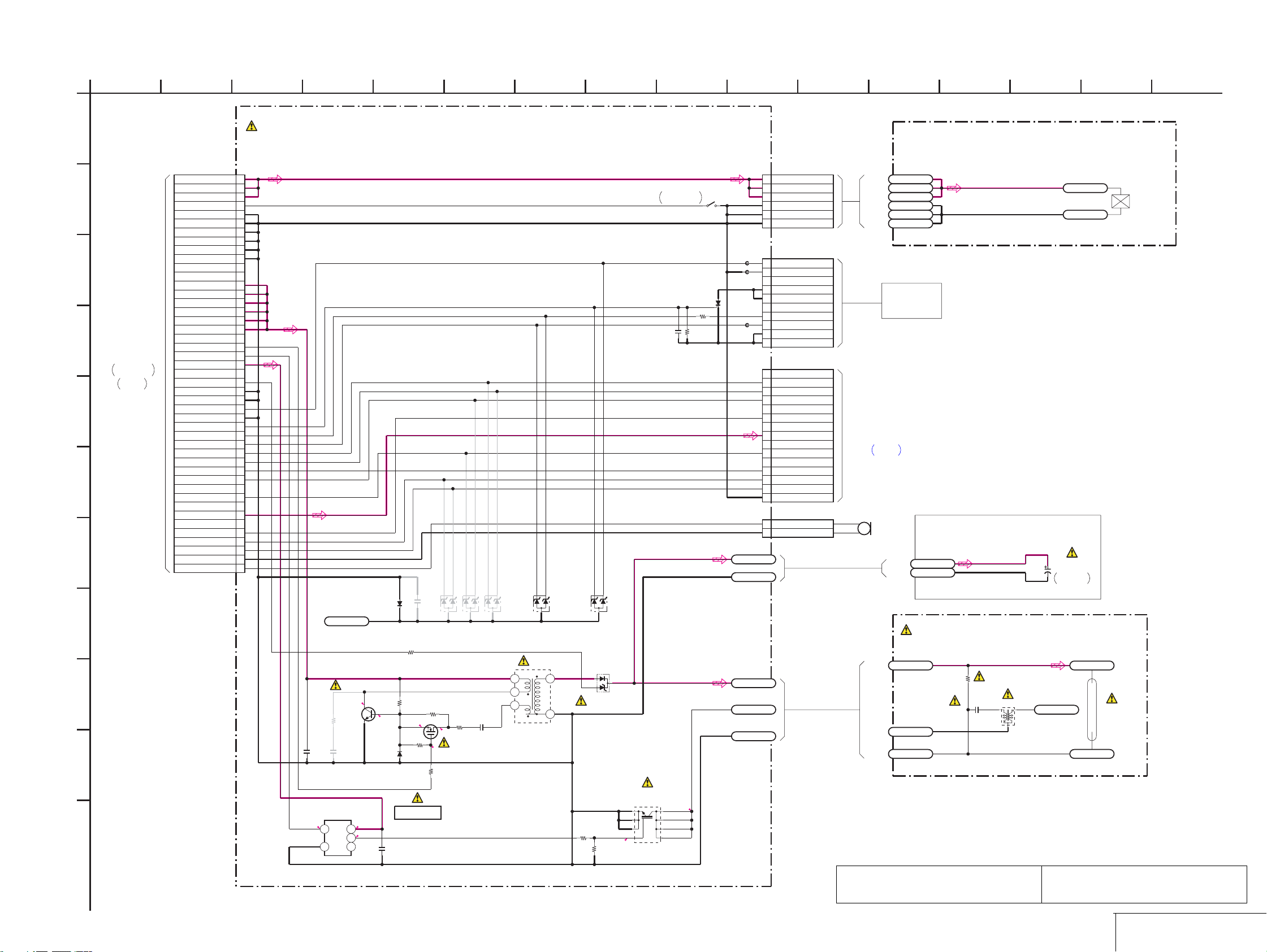
For Schematic Diagram
• Refer to page 4-61 for printed wiring board.
DSC-V3
1
A
3
ST-111 BOARD
4 1411 15
67
FLASH DRIVE (STROBE BLOCK)
XX MARK:NO MOUNT
CN006
45P
REG_GND
REG_GND
REG_GND
REG_GND
REG_GND
REG_GND
ST_UNREG
ST_UNREG
ST_UNREG
ST_UNREG
ST_UNREG
ST_UNREG
STRB_ON
ST_5V
STB_FULL
REG_GND
REG_GND
LANC_SIG
REG_GND
KEY_AD3
KEY_AD3C
XPWR_ON
EVER_3.0V
MIC_GND
MIC_SIG
45
44
43
42
41
40
39
38
37
36
35
N.C.
34
N.C.
33
32
31
30
29
28
27
N.C.
26
25
24
23
N.C.
22
21
20
19
18
17
HOT
16
15
14
13
12
11
10
N.C.
9
8
N.C.
7
6
N.C.
5
4
3
2
1
STRB_PLUNGER
STRB_PLUNGER
B
STRB_PLUNGER
XSTRB_POPUP
C
D
SY-106
(9/9)
CN751
THROUGH THE
FP-082 FLEXIBLE
PAGE 4-27
of LEVEL3
XSTRB_PWRSAVE
E
INTE_STRB_ON
LANC_JACK_IN2
MODE_DIAL1
F
G
MODE_DIAL0
PWR_LED_ON
Program_Dial_B
Program_Dial_A
H
I
C201
10u
J
6.3V
0 R5/P0
K
05
NO MARK:REC/PB MODE
LND001
STATIC_GND2
Q201,Q202
TRANS DRIVE
CPH3235-S-TL-E
0
R201
XX
C202
XX
IN
3
4
VDD
2
OUT
GND
1
5
NC
Q201
1
3
0
R:REC MODE
P:PB MODE
D007
MA111-(K8).S0
R206
4700
R202
5600
2
0
D201
MA111-(K8).S0
IC201
FLASH CONTROL
TND721MH5-S-TL-E
C204
0.1u
IC201
0
R203
100k
3
3
3
2
D001
XX
0
1
R207
560
Q202
MCH3405-TL-E
D002
2
1
1
D003
XX
XX
C203
0.22u
C002
XX
R204
1800
1
3
2
0
R205
10k
2
DF3A6.8FV(TH3SONY)
4
1
3
3
2
1
D004
T202
5
2
DF3A6.8FV(TH3SONY)
R208
47
R209
1M
4-35 4-36
8910
S201
STROBE
POP UP DETECT
FB001
0uH
FB002
0uH
D006
1
03P4J-T1
2
3
3
2
1
D005
1
2
D202
HAU160C030STP
3
GT8G133(T2LSONY.Q)
1
2
3
4
0
Q203
FLASH DRIVE
0.01u
C001
0R003
R002
1k
256
5
6
7
8
FB003
LND247
HOT
REG_GND
LND248
XE_H
XE_L
REG_GND
0uH
LND244
LND245
LND246
CN007
6
5
4
3
2
1
1
2
3
4
5
6
7
8
9
10
CN005
1
2
3
4
5
6
7
8
9
10
11
12
13
14
15
CN003
1
2
6P
STRB_PLUNGER
STRB_PLUNGER
STRB_PLUNGER
REG_GND
REG_GND
REG_GND
10P
CN004
LANC_SIG
REG_GND
N.C.
HOT
HOT
N.C.
INTE_STRB_ON
LANC_JACK_IN2
SHOE_GND
SHOE_GND
15P
N.C.
KEY_AD3
MODE_DIAL1
MODE_DIAL0
N.C.
PWR_LED_ON
N.C.
EVER_3.0V
N.C.
XPWR_ON
N.C.
KEY_AD3C
Program_Dial_B
Program_Dial_A
REG_GND
2P
MIC_SIG
REG_GND
THROUGH THE
HARNESS (HN-002)X2
THROUGH THE
HARNESS (HN-001)X3
122
13
PL-001 FLEXIBLE BOARD
PLUNGER
STRB_PLUNGER
6
LND008
STRB_PLUNGER
5
LND007
STRB_PLUNGER
4
LND006
3
BLOCK
PAGE 4-49
of LEVEL2
REG_GND
2
REG_GND
1
REG_GND
ADVANCED
ACCESSRY
SHOE
Note: C205 is not included in ST-111 complete board.
CHARGING CAPACITOR
LND201
HOT
LND202
REG_GND
LND005
LND004
LND003
CONTROL SWITCH
(SW51610)(MODE SW)
LND001-LND015
MIC901
MICROPHONE
MIC
FL-147 BOARD
FLASH UNIT
LND250
LND251
LND252
The components identified by mark 0 or dotted
line with mark 0 are critical for safety.
Replace only with part number specified.
REG_GND
XE_H
XE_L
Anode
C206
0.047u
R210
1M
L201
123
165
LND002
STRB_PLUNGER
LND246
TRIGGER
LND001
REG_GND
C205
135u
315V
CHARGING
CAPACITOR
Anode
CathodeCathode
LND244
XE_H
XE_L
LND245
FLASH
UNIT
PLUNGER
Les composants identifiés par une marque 0 sont
critiques pour la sécurité. Ne les remplacer que
par une piéce portant le numéro spécifié.
ST-111, FL-147, PL-001
Page 27

For Schematic Diagram
• Refer to page 4-63 for printed wiring board.
1
2
3
4 11
5
67
8910
CF-099 BOARD
A
CF/MS CONNECTOR
XX MARK:NO MOUNT
NO MARK:REC/PB MODE
B
MC_MSBS
MC_MSD1
MC_MSDIO
MC_MSD2
XMS_IN
MC_MSD3
MC_MSCLK
C
D
E
F
G
CF_D7
CF_XCE1
CF_XIORD
CF_IREQ
CF_A2
CF_A0
CF_D1
CF_XOE
CF_A08
CF_A07
CF_A04
CF_D8
CF_D10
CF_XCD2
R119
R117
R114
R112
R111
R109
R107
R106
R102
CN105 50P
50
MS-211
FLEXIBLE
CN002
PAGE 4-42
of LEVEL2
60P
CN101
2
VSS
4
MC_MSBS
6
MC_MSD1
8
MC_MSDIO
10
MC_MSD2
12
XMS_IN
14
MC_MSD3
16
MC_MSCLK
18
MS_VCC
20
47
47
47
47
47
47
47
47
47
VSS
22
D07
24
XCE1
26
XIORD
28
IREQ
30
A02
32
A00
34
D01
36
GND
38
GND
40
GND CF_VCC
42
XOE
44
A08
46
A07
48
A04
50
D08
52
D10
54
XCD2
56
XACCESS_LED
58
MS_PWR_ON
60
XRESET_FR
XCD1
XCE2
XIOWR
CF_VCC
CF_VCC
RESET
XWAIT
XREG
XIOIS16
GND
XWE
1
D03
D11
D04
D12
D05
D13
D06
D14
D15
A05
A01
D00
D02
A10
A09
A06
A03
D09
R127
3
R126
5
R125
7
R124
9
R123
11
R122
13
R121
15
R120
17
R118
19
R116
21
R113
23
25
R110
27
R108
29
R105
31
33
35
37
39
41
43
45
47
R103
49
51
53
55
57
59
CF_XCD1
CF_D3
47
CF_D11
47
CF_D4
47
CF_D12
47
CF_D5
47
CF_D13
47
CF_D6
47
CF_D14
47
CF_D15
47
CF_XCE2
47
CF_XIOWR
47
CF_A05
CF_A1
47
CF_D0
47
CF_D2
47
CF_A10
CF_A09
CF_XWE
CF_A06
CF_A03
CF_D9
47
CF_RESET
CF_XWAIT
CF_XREG
CF_XIOIS16
L101
1uH
CF_XCD2
CF_D10
CF_XIOIS16
CF_D9
CF_D2
CF_D8
CF_D1
CF_D0
CF_A0
CF_XREG
CF_A1
CF_A2
CF_XWAIT
CF_A03
CF_RESET
CF_A04
CF_A05
CF_A06
CF_IREQ
CF_A07
CF_XWE
CF_A08
CF_XIOWR
CF_A09
CF_XIORD
CF_XOE
CF_A10
CF_XCE2
CF_XCE1
CF_D15
CF_D7
CF_D14
CF_D6
CF_D13
CF_D5
CF_D12
CF_D4
CF_D11
CF_D3
CF_XCD1
CL102
R104
CL103
CL104
CL105
0
CL101
C101
0.1u
C102
0.1u
XXC104
GND
25
XCD2
D10
49
24
XIOIS16
48
D09
D02
23
47
D08
22
D01
46
XSTSCHG
21
D00
45
XSPKR
A00
20
XREG
44
19
A01
43
XINPACK
A02
18
42
XWAIT
17
A03
41
RESET
16
A04
40
XVS2
15
A05
XCSEL
39
14
A06
38
VCC
VCC
13
IREQ
37
A07
12
36
XWE
A08
11
35
XIOWR
10
A09
34
XIORD
9
XOE
33
XVS1
A10
8
XCE2
32
7
XCE1
31
D15
D07
6
D14
30
5
D06
29
D13
4
D05
28
D12
D04
3
D11
27
D03
2
26
XCD1
GND
1
CF CARD
COMPACT FLASH
TYPE I
DSC-V3
H
I
J
4-37
MAZS082008SO
MA2S111-(K8).SO
D105
CL-270HR-C-TS
(ACCESS)
MA2S111-(K8).SO
D104
D106
D103
4-38
MC_MSCLK
MC_MSD3
XMS_IN
MC_MSD2
MC_MSDIO
MC_MSD1
MC_MSBS
CN104
10
9
8
7
6
5
4
3
2
1
R101
XX
R133
XX
12P
VSS
VCC
SCLK
DATA3
INT
DATA2
SDIO/DATA0
DATA1
MS_BS
VSS
LND101
STATIC GND
LND102
STATIC GND
11
MEMORY
STICK
MEMORY
STICK
12
CF-099
C107
0.1u
R130
R132
390
R131
C103
47u
6.3V
0
0
S101
RESET
Q102
SSM6E01TU
B+ SWITCH
2.9
R129
3300
3
6
R128
220k
C106
22u
6.3V
C105
Q101
DTA144EMT2L
LED DRIVE
2.9
R115
2200
05
0.1u
2.9
0
2.9
4
5
0.10.1
1
2
2.9
D102
MA2SD32008S0
Page 28
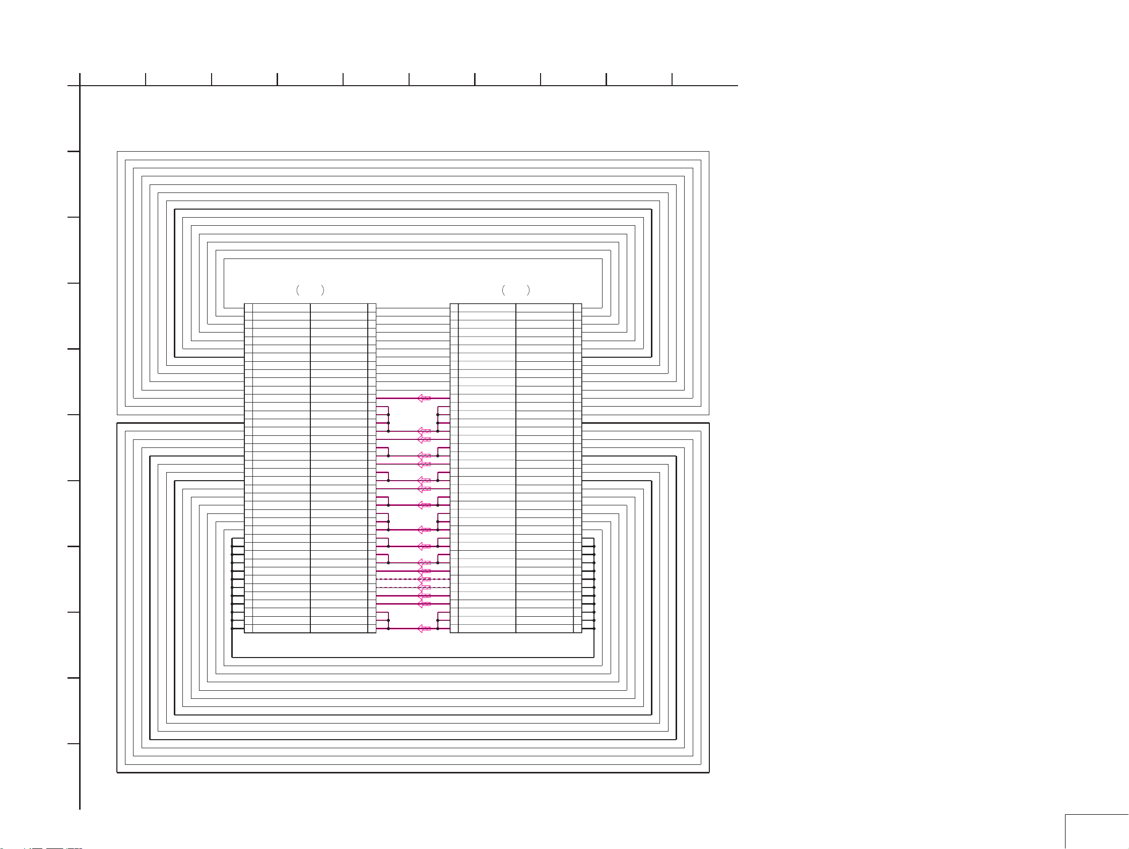
For Schematic Diagram
• Refer to page 4-63 for printed wiring board.
1
BB-005 FLEXIBLE BOARD
A
SY-DD EXTENSION BOARD
B
C
D
E
F
G
H
I
3
80
MODE_DIAL0
78
MODE_DIAL1
76
XRSTX
74
SYS_V
72
FR_INT
70
XUSB_JACK_IN
68
REG_GND
66
XLANC_JACK_IN_FR
64
XMS_IN
62
XPWR_LED_ON
60
MC_UPDATE
58
XLANC_PWR_ON
56
XCS_MC M_5V
54
XCHARGE/XSTRB_LED
52
REG_GND
50
FR_SO
48
FR_SI
46
XFR_SCK
44
REG_GND
42
LANC_OUT
40
LANC_IN
38
REG_GND
36
BL_L
34
BL_THH
32
BL_LEVEL
30
BL_H
28
XSHTR_ON
26
XAE_LOCK_ON
24
REG_GND A_3.1V
22
REG_GND
20
REG_GND CAM_15V
18
REG_GND
16
REG_GND
14
REG_GND
12
REG_GND
10
REG_GND
8
REG_GND
6
REG_GND
4
2
REG_GND
410
SY-106
(8/9)
CN701
PAGE 4-25
of LEVEL3
CN301
80P
5
79
KEY_AD4
77
KEY_AD3
75
KEY_AD2
73
KEY_AD1
71
KEY_AD0
69
XPWR_ON
67
XSYS_RST
65
N.C
CAM_5V
CF_3.3V
CF_3.3V
D_2.8V
D_2.8V
ST_5V
A_2.8V
A_2.8V
D_1.2V
D_1.2V
D_1.2V
A_3.1V
CAM_15V
CAM_-8.0V
CAM_-0.5V
EVER_3.0V
LANC_5.5V
ST_UNREG
ST_UNREGREG_GND
ST_UNREG
M_5V
M_5V
M_5V
63
61
59
57
55
53
51
49
47
45
43
41
39
37
35
33
31
29
27
25
23
21
19
17
15
13
11
9
7
5
3
1
XLANC_IC_ON
XU_DRIVE_IN
XAV_JACK_IN
SDRAM_2.8V SDRAM_2.8V
PANEL_4.9V
PANEL_8.5V
62 9
79
KEY_AD4
77
KEY_AD3
75
KEY_AD2
73
KEY_AD1
71
KEY_AD0
69
XPWR_ON
67
XSYS_RST
65
N.C
63
XLANC_IC_ON
61
XU_DRIVE_IN
59
XAV_JACK_IN
57
55
M_5V
53
M_5V
51
M_5V
49
M_5V
47
CAM_5V
45
CF_3.3V
43
CF_3.3V
PANEL_4.9V
41
D_2.8V
39
D_2.8V
37
ST_5V
35
33
A_2.8V
31
A_2.8V
29
D_1.2V
27
D_1.2V
25
D_1.2V
23
A_3.1V
21
A_3.1V
19
CAM_15V
CAM_15V
17
15
PANEL_8.5V
13
CAM_-8.0V
CAM_-0.5V
11
9
EVER_3.0V
LANC_5.5V
7
ST_UNREG
5
ST_UNREG
3
ST_UNREG
1
7
DD-217
PAGE 4-33
of LEVEL3
CN302
(3/3)
CN084
80P
MODE_DIAL0
MODE_DIAL1
XUSB_JACK_IN
REG_GND
XLANC_JACK_IN_FR
XMS_IN
XPWR_LED_ON
MC_UPDATE
XLANC_PWR_ON
XCS_MC
XCHARGE/XSTRB_LED
REG_GND
XFR_SCK
REG_GND
LANC_OUT
LANC_IN
REG_GND
BL_THH
BL_LEVEL
XSHTR_ON
XAE_LOCK_ON
REG_GND
REG_GND
REG_GND
REG_GND
REG_GND
REG_GND
REG_GND
REG_GND
REG_GND
REG_GND
REG_GND
REG_GND
XRSTX
SYS_V
FR_INT
FR_SO
FR_SI
BL_H
BL_L
8
80
78
76
74
72
70
68
66
64
62
60
58
56
54
52
50
48
46
44
42
40
38
36
34
32
30
28
26
24
22
20
18
16
14
12
10
8
6
4
2
DSC-V3
J
K
05
4-39
4-40
BB-005
Page 29

For Schematic Diagram
• Refer to page 4-64 for printed wiring board.
1
2 9
3
4
5
6
7
810
MS-211 FLEXIBLE BOARD
A
B
C
D
E
F
G
SY-CF EXTENSION BOARD
SY-106
(8/9)
CN704
PAGE 4-26
of LEVEL3
CN001
2
VSS
4
MC_MSBS
6
MC_MSD1
8
MC_MSDIO
10
MC_MSD2
12
XMS_IN
14
MC_MSD3 D13
16
MC_MSCLK
18
MS_VCC
20
VSS
22
D07
24
XCE1
26
XIORD
28
IREQ
30
A02
32
A00
34
D01
36
GND
38
GND
40
GND
42
XOE
44
A08
46
A07
48
A04
50
D08
52
D10
54
XCD2
56
XACCESS_LED
58
MS_PWR_ON
60
XRESET_FR
60P
XCD1
XCE2
XIOWR
CF_VCC
CF_VCC
CF_VCC
XWE
RESET
XWAIT
XREG
XIOIS16
GND
CF-099
CN101
PAGE 4-37
of LEVEL2
60PCN002
XMS_IN
MS_VCC
XCE1
XIORD
XCD2
D07
IREQ
D01
GND
GND
GND
XOE
A08
D08
D10
VSS
VSS
A02
A00
A07
A04
2
4
6
8
10
12
14
16
18
20
22
24
26
28
30
32
34
36
38
40
42
44
46
48
50
52
54
56
58
60
1
3
D03
5
D11
7
D04
9
D12
11
D05
13
15
D06
17
D14
19
D15
21
23
25
A05
27
A01
29
D00
31
D02
33
A10
35
37
39
41
A09
43
45
A06
47
A03
49
D09
51
53
55
57
59
1
XCD1
3
D03
5
D11
7
D04
9
D12
11
D05
13
D13
15
D06
17
D14
19
D15
21
XCE2
23
XIOWR
25
A05
27
A01
29
D00
31
D02
33
A10
35
CF_VCC
37
CF_VCC
39
CF_VCC
41
A09
43
XWE
45
A06
47
A03
49
D09
51
RESET
53
XWAIT
55
XREG
57
XIOIS16
59
MC_MSBS
MC_MSD1
MC_MSDIO
MC_MSD2
MC_MSD3
MC_MSCLK
XACCESS_LED
MS_PWR_ON
XRESET_FRGND
DSC-V3
H
I
05
4-41
4-42
MS-211
Page 30

For Schematic Diagram
• Refer to page 4-65 for printed wiring board.
1
2675
3
4
JK-269 FLEXIBLE BOARD
A
B
C
D
E
F
USB, A/V JACK (JK BLOCK)
XX MARK:NO MOUNT
J102
ACC
CN101
6
USB
7
J103
A/V OUT
(MONO)
GND
VCC
D203
CL-330IRS-X-TU
(IR EMITTER)
D204
R206
470
4
1
5
2
3
7P
5
ID
4
D+
3
D-
2
1
3
1
2
4
CL-196HR-CD-T
(SELF TIMER)
R101
0
FB107
FB101
FB108
S101
LENS ADAPTOR
DETECT
(RED)
FB103
1
IR_LED_A
2
IR_LED_K
3
SELF_TIMER_LED
4
5
LANC_DC
XLANC_JACK_IN
6
REG_GND(N.C)
7
LANC_SIG
8
REG_GND(N.C)
9
ACC_STRB_ON
FB106
2
3
1
LND150
STATIC_GND
10
11
12
13
14
15
16
17
18
19
20
21
22
23
24
25
26
27
REG_GND
USB_JACK_IN
REG_GND
USB_D-
USB_D+
REG_GND
REG_GND
REG_GND(N.C)
A_OUT
REG_GND(N.C)
V_OUT
REG_GND
XAV_JACK_IN
REG_GND
KEY_AD3C
D2.8V
N.C
N.C
LND101
LND102
LND103
LND104
LND105
LND106
LND107
LND108
LND109
LND110
LND111
LND112
LND113
LND114
LND115
LND116
LND117
LND118
LND119
LND120
LND121
LND122
LND123
LND124
LND125
LND126
LND127
SY-106
(9/9)
CN752
PAGE 4-27
of LEVEL3
DSC-V3
05
4-43
The components identified by mark 0 or dotted
line with mark 0 are critical for safety.
Replace only with part number specified.
4-44
Les composants identifiés par une marque 0 sont
critiques pour la sécurité. Ne les remplacer que
par une piéce portant le numéro spécifié.
JK-269
Page 31

For Schematic Diagram
LND019
BATT_GND
LND018
BATT_GND
LND017
BATT_GND
LND016
BATT_GND
LND015
BATT_GND
LND012
BATT_GND
LND014
BATT_GND
LND013
BATT_GND
LND011
BATT_SIG
LND010
BATT_UNREG
LND009
BATT_UNREG
LND008
BATT_UNREG
LND007
BATT_UNREG
LND005
BATT_UNREG
LND004
BATT_UNREG
LND006
BATT_UNREG
S
BT001
1
A
11
6
7
14
15
1
8
3
2
1
3
2
5
4
13
16
12
9
10
BATTERY
TARMINAL
DD-217
(2/3)
PAGE 4-31
B
4
XX MARK:NO MOUNT
05
BT-026 FLEXIBLE BOARD
C
of LEVEL3
BATTERY IN
CN001
32
LND005
N.C.
LND006
N.C.
LND003
VL_GND
LND004
VL_GND
LND001
VL_GND
LND002
VL_GND
BT001
LND007
N.C.
LND008
VL_3V
LND009
VL_3V
LND010
VL_3V
LND011
VL_3V
1
A
LITHIUM
BATTERY
DD-217
(3/3)
PAGE 4-33
B
4
XX MARK:NO MOUNT
05
LI-072 FLEXIBLE BOARD
C
of LEVEL3
LITHIUM BATTERY
CN083
32
2
10
5
9
1
6
3
7
11
4
8
• Refer to page 4-66 for printed wiring board.
For Schematic Diagram
• Refer to page 4-66 for printed wiring board.
1
32
4
AF-008 FLEXIBLE BOARD
A
B
C
AF LASER
XX MARK:NO MOUNT
05
1
LD
2
PD
D109
(LASER UNIT)
(Note)
3
KCOM
GND
GND
GND
N.C.
N.C.
LD
LD
N.C.
N.C.
PD
PD
1
LND001
LND002
2
LND003
3
LND004
4
5
LND005
LND006
6
LND007
7
LND008
8
LND009
9
LND010
10
LND011
11
SY-106
(9/9)
CN763
PAGE 4-28
of LEVEL3
DSC-V3
For Schematic Diagram
• Refer to page 4-66 for printed wiring board.
1
2
RE-003 FLEXIBLE BOARD
A
B
C
SHUTTER SWITCH
XX MARK:NO MOUNT
S001
(SHUTTER)
NO
1
4
05
XAE_LOCK_ON
3
2
XSHTR_ON
4-45
For Schematic Diagram
• Refer to page 4-66 for printed wiring board.
3
N.C.
XSHTR_ON
N.C.
REG_GND
REG_GND
XAE_LOCK_ON
6
LND001
LND002
5
LND003
4
LND004
3
LND005
2
LND006
1
DD-217
(3/3)
CN085
PAGE 4-34
of LEVEL3
4
(Note) Be sure to read “SERVICE NOTE” on page 1-2
when replacing the laser unit (D109).
The components identified by mark 0 or dotted
line with mark 0 are critical for safety.
Replace only with part number specified.
4-46
Les composants identifiés par une marque 0 sont
critiques pour la sécurité. Ne les remplacer que
par une piéce portant le numéro spécifié.
AF-008, BT-026, RE-003, LI-072
Page 32

1
53
62
74
CONTROL SWITCH BLOCK
A
(SW51610) (REAR SW)
R014
6800
R002
3300
CONTROL SWITCH BLOCK (SW51610) (REAR SW) is replaced
as block, so that PRINTED WIRING BOARD is omitted.
S016
CF
MS
B
MSCF
12
11
10
9
8
7
6
5
4
3
2
1
REG_GND
KEY_AD0
KEY_AD4
KEY_AD2
XTALLY_LED
D_2.8V
AE_LOCK_LED
XCHARGE_LED
EVER_3.0V
KEY_AD1
REG_GND
N.C.
S011
T (FLASH)
LND012
LND011
LND010
LND009
SY-106
C
(8/9)
CN703
PAGE 4-25
of LEVEL3
LND008
LND007
LND006
LND005
LND004
LND003
LND002
LND001
R003
1500
R004
1200
R001
1200
S012
(ZOOM)
TLRMV1021(T15SOY,F)
(SELF TIMER/RECORDING)
W
D106
(RED)
R005
1500
S005
IMAGE SIZE/
DELETE
S004
MENU
S003
(REVIEW)
S002
DISPLAY/
LCD SCREEN ON/OFF
S001
(MACRO)
R009
3300
S013
R011
1200
S014
(SET)
R016
6800
R015
3300
R007
1500
R008
1200
R010
6800
S015
(SELF TIMER)
S010
EXPOSURE
S009
FOCUS
S008
FRAME
S007
AE LOCK
D
D107
TLGV1021(T15SOY2,F)
(AE/AF LOCK)
(GREEN)
R012
470
D108
TLYV1021(T15SOY,F)
R013
820
CHG/
(YELLOW)
E
05
DSC-V3
4-47
4-48
SW51610 (REAR SW)
Page 33

1
53
62
74
CONTROL SWITCH BLOCK
A
(SW51610) (MODE SW)
CONTROL SWITCH BLOCK (SW51610) (MODE SW) is replaced
as block, so that PRINTED WIRING BOARD is omitted.
S105
NIGHTFRAMING/
NIGHTSHOT
R112
3300
B
C
D
ST-111
CN005
PAGE 4-36
of LEVEL2
LND001
LND002
LND003
LND004
LND005
LND006
LND007
LND008
LND009
LND010
LND011
LND012
LND013
LND014
LND015
1
2
3
MODE_DIAL1
4
MODE_DIAL0
5
6
PWR_LED_ON
7
8
9
10
11
12
Program_Dial_B
13
Program_Dial_A
14
15
KEY_AD3
EVER_3.0V
XPWR_ON
KEY_AD3C
REG_GND
N.C
N.C
N.C
N.C
N.C
R109
270
R105
1200
D110
TLGV1021(T15SOY2,F)
(POWER)
(GREEN)
R106
1500
R107
3300
R108
6800
S106
(JOG DIAL)
SCENE
SET_UP
MOVIE
PLAY
AUTO
DIAL_A
EXECUTE
10
4
3
2
1
MANUAL
AE-A
AE-S
P_AUTO
R115
1200
R113
1500
R114
1200
5
A
6
B
C
S104
(MODE DIAL)
S103
POWER
DSC-V3
4-49
E
05
4-50
DIAL_B
SW51610 (MODE SW)
Page 34

Link
Link
4-3. PRINTED WIRING BOARDS
CD-515 FLEXIBLE BOARD
CD-515 FLEXIBLE BOARD
ST-111 BOARD
ST-111 BOARD
FL-147 BOARD
FL-147 BOARD
PL-001 FLEXIBLE BOARD
PL-001 FLEXIBLE BOARD
CF-099 BOARD
CF-099 BOARD
BB-005 FLEXIBLE BOARD
BB-005 FLEXIBLE BOARD
COMMON NOTE FOR PRINTED WIRING BOARDS
COMMON NOTE FOR PRINTED WIRING BOARDS
MOUNTED PARTS LOCATION
MOUNTED PARTS LOCATION
CIRCUIT BOARDS LOCATION
CIRCUIT BOARDS LOCATION
MS-211 FLEXIBLE BOARD
MS-211 FLEXIBLE BOARD
JK-269 FLEXIBLE BOARD
JK-269 FLEXIBLE BOARD
AF-008 FLEXIBLE BOARD
AF-008 FLEXIBLE BOARD
BT-026 FLEXIBLE BOARD
BT-026 FLEXIBLE BOARD
RE-003 FLEXIBLE BOARD
RE-003 FLEXIBLE BOARD
LI-072 FLEXIBLE BOARD
LI-072 FLEXIBLE BOARD
Board Name Function
CD-515 FLEXIBLE CCD IMAGER
ST-111 FLASH DRIVE
FL-147 FLASH UNIT
PL-001 FLEXIBLE PLUNGER
CF-099 CF/MS CONNECTOR
BB-005 FLEXIBLE SY-DD EXTENSION BOARD
MS-211 FLEXIBLE SY-CF EXTENSION BOARD
JK-269 FLEXIBLE USB, A/V JACK
AF-008 FLEXIBLE AF LASER
BT-026 FLEXIBLE BATTERY IN
RE-003 FLEXIBLE SHUTTER SWITCH
LI-072 FLEXIBLE LITHIUM BATTERY
DSC-V3
Page 35

4-3. PRINTED WIRING BOARDS
4-3. PRINTED WIRING BOARDS
4-3. PRINTED WIRING BOARDS
THIS NOTE IS COMMON FOR PRINTED WIRING BOARDS
• : Uses unleaded solder.
•
: Circuit board
: Flexible board
• Chip parts.
Transistor Diode
C
654
46
45
Pattern from the side which enables seeing.
: pattern of the rear side
(The other layers’ patterns are not indicated)
• Through hole is omitted.
EB
123
3152
21
312
23
12
• Circled numbers refer to waveforms.
• There are a few cases that the part printed on diagram
345
14
534
isn’t mounted in this model.
• C: panel designation
Board Name Parts Location
Total Number of Layers Layers Not Indicated
Pattern
CD-515 flexible 4-71 2 layers –
ST-111 4-73 4 layers 2 to 3 layers
FL-147 – 4 layers 2 to 3 layers
PL-001 flexible – 1 layers –
CF-099 4-71 4 layers 2 to 3 layers
BB-005 flexible – 2 layers –
MS-211 flexible – 2 layers –
JK-269 flexible – 1 layer –
AF-008 flexible – 1 layer –
BT-026 flexible – 1 layer –
RE-003 flexible – 1 layer –
LI-072 flexible – 1 layer –
54
21321321
123
43
12
23
14
3
4
3
12
31
4625
654
46
123
3152
DSC-V3
4-51
Page 36

CD-515 FLEXIBLE
CD-515
---
CCCCC
BBB
C
C
Note for Printed Wiring Board (See page 4-51).
: Uses unleaded solder.
CD-515 FLEXIBLE BOARD
LND131
LND123
LND125
LND127
LND129
LND133
LND135
LND137
LND139
LND121
LND119
LND117
LND113
LND115
LND111
LND107
LND109
LND103
LND105
LND101
A
B
C
R117
Q104
R115
R116
LND138
LND136
R114
LND132
LND134
R104
R118
Q102
LND128
LND130
R119
Q105
R111
C108
LND124
LND126
C112
LND120
LND122
Q103
R110
R113
C107
LND116
LND118
R103
R106
C105
LND112
LND114
C103
LND108
LND110
R112
LND104
LND106
C111
LND102
Note: IC101 is not included in
CD-515 flexible complete board.
14
1
IC101
FB101
C109
C110
+
15
28
B
DSC-V3
05
1 2 3
1-864-452-
11
4-544-53
CD-515
Page 37

Printed wiring boards of the CH-146, SY -106 and DD-217 boards are not shown.
Pages from 4-55 to 4-60 are not shown.
DSC-V3
Page 38

PL-001 FLEXIBLE
Note for Printed Wiring Board (See page 4-51).
: Uses unleaded solder.
ST-111, FL-147
Note for Printed Wiring Board (See page 4-51).
: Uses unleaded solder.
FL-147 BOARD
31
LND245
ST-111 BOARD (SIDE A)
LND245
58
LND246
LND247
A
Q203
1
R208
4
R209
LND248
B
LND246
LND250
L201
XE L
XE L
XE H
REG GND
LND244
LND251
TRIGGER
2
LND252
FLASH UNIT
C206
S201
FB001
1
6
CN007
R210
LND244
1-864-448-
FB002
XE H
11
S201
STROBE
POP UP DETECT
21
CN003
1
CN004
PL-001 FLEXIBLE BOARD
PL-001
LND001 LND002
1-864-454-
PLUNGER
11
05
LND007
LND008
LND005
LND006
LND003
LND004
1-864-454-
ST-111 BOARD (SIDE B)
EP-GW
1-864-447-
C201
R207
LND001
1
D003
23
1-864-447-
10
11
115
CN005
FB003
D001
2
1
D004
3
3
1
2
1
3
2
D002
2
14
2
1
C002
R003
D007
D005
3
1
2
Q202
G
R203
R205
CN006
R204
D
S
R202
D201
C203
B
Q201
E
44
45
3
2
C
1
R201
C202
T202
R206
4
1
5
2
D202
R002
IC201
3
C001
5
4
3
1
C204
3
1
D006
2
A
B
DSC-V3
05
1 2 3 4
REG GND
HOT
+
C205
CHARGING
CAPACITOR
Note: C205 is not included in
ST-111 complete board.
05
234
4-624-61
1-864-447-
1
11
ST-111, FL-147, PL-001
Page 39

CF-099
1
4
6
<
0
-
-
4
1
Note for Printed Wiring Board (See page 4-51).
: Uses unleaded solder.
CF-099 BOARD (SIDE A)
R103
A
R102
24
502549
B
C
R105
R107
R106
R108
CL103
CL104
R109
CL105
R110
R104
R111
C104
CL101
C101
C102
CN105
R112
R113
R114
R116
R117
R118
R119
R120
R121
R122
R123
R124
R125
CF-099 BOARD (SIDE B)
R127
+
B
C103
R126
L101
CL102
1
25101520
2630354045
1
2
1
CN104
10
R115
C105
D106
R128
D103
R131
+
A
C106
13
Q102
64
D102
CN101
60
59
11
12
R130
C107
R129
R101
A
B
C
D
05
1 2 3 4
BB-005 FLEXIBLE
Note for Printed Wiring Board (See page 4-51).
: Uses unleaded solder.
BB-005 FLEXIBLE BOARD
2
1
CN302
1-864-446-
1
CN301
D104
LND102
B
E
C
Q101
D105
D105
(ACCESS)
S101
R132
AK
S101
RESET
R133
11
05
LND101
1-864-446-
1234
D
11
MS-211 FLEXIBLE BOARD
MS-211 FLEXIBLE
1
Note for Printed Wiring Board (See page 4-51).
: Uses unleaded solder.
280
2
1
1-864-450-
2
CN001
59
60
8
11
CN002
80
05
DSC-V3
79
79
1-864-451-
60
11
05
59
4-63 4-64
CF-099, BB-005, MS-211
Page 40

JK-269 FLEXIBLE
D
1
<
J
9
A
AF-008 FLEXIBLE
BT-026 FLEXIBLE
Note for Printed Wiring Board (See page 4-51).
: Uses unleaded solder.
JK-269 FLEXIBLE BOARD
LND101
LND102
LND103
LND104
LND105
LND106
LND107
LND108
LND109
LND110
LND111
LND112
LND113
LND114
LND115
LND116
LND117
LND118
LND119
LND120
LND121
LND122
LND123
LND124
LND125
LND126
LND127
05
S101
LENS ADAPTOR
DETECT
(IR EMITTER)
2
1
S101
3
D203
FB107
D203
1
FB103
FB101
R101
2
LND150
FB108
D204
A
R206
CN101
J102J103
K
-864-449-
I
FB106
6
7
4
3
D204
(SELF TIMER)
CN101
(USB)
J103
A/V OUT
(MONO)
J102
ACC
Note for Printed Wiring Board (See page 4-51).
: Uses unleaded solder.
(Note) Be sure to read “SERVICE NOTE” on page 1-2
when replacing the laser unit (D109).
AF-008 FLEXIBLE BOARD
3
2
1
D109
(LASER UNIT)
(Note)
1-864-457-AF-008
1-864-457-
05
LND001
LND002
LND003
LND004
LND005
LND006
LND007
LND008
LND009
LND010
11
LND011
Note for Printed Wiring Board (See page 4-51).
: Uses unleaded solder.
BT-026 FLEXIBLE BOARD
LND010
LND004
LND005
LND006
LND007
LND008
LND009
LND011
LND012
LND013
LND014
LND015
LND016
LND017
LND018
LND019
BT-026
3
BT001
05
1
1-864-455-
1-864-455-
11
LI-072 FLEXIBLE
Note for Printed Wiring Board (See page 4-51).
: Uses unleaded solder.
LI-072 FLEXIBLE BOARD
LND008
LND010
LND002
LND004
LND011
LND009
LND001
LND003
K-26
>PI
1-864-449-
11
RE-003 FLEXIBLE BOARD
4
3
S001
(SHUTTER)
RE-003
S001
2
1
LI-072
1-864-456-
BT001
BATTERY,
LITHIUM SECONDARY
RE-003 FLEXIBLE
1-864-453-
Note for Printed Wiring Board
(See page 4-51).
: Uses unleaded solder.
1-864-453-
LND006
LND005
LND003
LND001
05
DSC-V3
11
05
BT001
1-864-456-
11
CAUTION
Danger of explosion if battery is incorrectly replaced.
Replace only with the same or equivalent type.
4-664-65
JK-269, AF-008, BT-026, RE-003, LI-072
Page 41

Waveforms of the SY -106 and DD-217 boards are not sho wn.
Page 4-69 and 4-70 are not shown.
DSC-V3
Page 42

4-3. PRINTED WIRING BOARDS
4-3. PRINTED WIRING BOARDS
4-5. MOUNTED PARTS LOCATION
CD-515 FLEXIBLE BOARD
C107 C-1
C108 C-1
C109 C-3
C110 C-3
FB101 C-3
Q102 C-1
Q103 B-1
Q104 C-1
Q105 C-1
R103 B-1
R104 B-1
R106 C-1
R110 B-1
R111 C-1
R112 C-2
R113 C-1
R114 B-1
R115 C-1
R116 C-1
R117 C-1
R118 C-1
R119 B-1
CF-099 BOARD
C101 A-2
C102 A-2
* C103 A-4
* C105 B-1
* C106 B-1
* C107 B-1
* CN101 B-4
* CN104 B-2
CN105 A-3
* D102 B-1
* D103 B-1
* D104 C-4
* D105 D-3
* D106 A-1
* L101 A-4
* Q101 D-4
* Q102 B-1
R102 A-1
R103 A-1
R104 A-2
R105 A-1
R106 A-2
R107 A-2
R108 A-2
R109 A-2
R110 A-2
R111 A-2
R112 A-3
R113 A-3
R114 A-3
* R115 B-1
R116 A-3
R117 A-3
R118 A-3
R119 A-3
R120 A-3
R121 A-3
R122 A-3
R123 A-3
R124 A-3
R125 A-3
* R126 A-4
* R127 A-4
* R128 B-1
* R129 B-1
* R130 B-1
* R131 B-1
* R132 D-4
* S101 D-4
no mark : side A
mark : side B
*
DSC-V3
4-71
CD-515, CF-099
Page 43

Mounted parts location of the SY -106 and DD-217 board is not shown.
Page 4-72 is not shown.
DSC-V3
Page 44

ST-111 BOARD
* C001 B-1
* C201 A-1
* C203 A-2
* C204 A-1
CN003 A-3
CN004 B-4
* CN005 B-4
* CN006 B-3
CN007 B-3
* D004 A-3
* D005 A-3
* D006 A-1
* D007 A-3
* D201 A-3
* D202 A-1
FB001 A-3
FB002 A-3
* FB003 A-3
* IC201 A-1
* Q201 A-2
* Q202 A-3
Q203 A-1
* R002 B-1
* R003 A-3
* R202 A-3
* R203 A-3
* R204 A-3
* R205 A-3
* R206 B-2
* R207 A-3
R208 A-1
R209 A-1
S201 A-3
* T202 A-2
4-3. PRINTED WIRING BOARDS
4-3. PRINTED WIRING BOARDS
no mark : side A
mark : side B
*
DSC-V3
4-73E
ST-111
Page 45

NOTE
GRIP BLOCK
GRIP BLOCK
NOTE
5. REPAIR PARTS LIST
NOTE: Characters A to Z of the electrical parts list indicate location of exploded views in which the desired part is shown.
Link
Link
MAIN BLOCK
MAIN BLOCK
CABINET (UPPER) BLOCK
CABINET (UPPER) BLOCK
EXPLODED VIEWS
EXPLODED VIEWS
ABC
CABINET (FRONT) BLOCK
CABINET (FRONT) BLOCK
EF
CABINET (REAR) BLOCK
CABINET (REAR) BLOCK
LENS BLOCK
LENS BLOCK
D
Link
Link
AF-008 FLEXIBLE BOARD
AF-008 FLEXIBLE BOARD
BB-005 FLEXIBLE BOARD
BB-005 FLEXIBLE BOARD
BT-026 FLEXIBLE BOARD
BT-026 FLEXIBLE BOARD
ACCESSORIES
ELECTRICAL PARTS LIST
ELECTRICAL PARTS LIST
A
C
C
DCE
CF-099 BOARD
CF-099 BOARD
FL-147 BOARD
FL-147 BOARD
JK-269 FLEXIBLE BOARD
JK-269 FLEXIBLE BOARD
LI-072 FLEXIBLE BOARD ST-111 BOARDCD-515 FLEXIBLE BOARD
LI-072 FLEXIBLE BOARD ST-111 BOARDCD-515 FLEXIBLE BOARD
C
E
B
MS-211 FLEXIBLE BOARD
MS-211 FLEXIBLE BOARD
PL-001 FLEXIBLE BOARD
PL-001 FLEXIBLE BOARD
RE-003 FLEXIBLE BOARD
RE-003 FLEXIBLE BOARD
ACCESSORIES
C
E
C
DSC-V3
Page 46

5. REPAIR PARTS LIST
5. REPAIR PARTS LIST
5. REPAIR PARTS LIST
NOTE:
• -XX, -X mean standardized parts, so they may have some differences from
the original one.
• Items marked “*” are not stocked since they are seldom required for routine
service. Some delay should be anticipated when ordering these items.
• The mechanical parts with no reference number in the exploded views are not
supplied.
• Due to standardization, replacements in the parts list may be different from
the parts specified in the diagrams or the components used on the set.
• CAPACITORS:
uF: µF
• COILS
uH: µH
• RESISTORS
All resistors are in ohms.
METAL: metal-film resistor
METAL OXIDE: Metal Oxide-film resistor
F: nonflammable
• SEMICONDUCTORS
In each case, u: µ, for example:
uA...: µA... , uPA... , µPA... ,
uPB... , µPB... , µPC... , µPC... ,
uPD..., µPD...
• Abbreviation
AUS: Australian model
CH : Chinese model
CND: Canadian model
HK : Hong Kong model
J: Japanese model
JE : Tourist model
KR : Korean model
When indicating parts by reference number,
please include the board name.
The components identified by mark 0 or
dotted line with mark 0 are critical for safety.
Replace only with part number specified.
Les composants identifiés par une marque
0 sont critiques pour la sécurité.
Ne les remplacer que par une pièce portant
le numéro spécifié.
DSC-V3
5-1
Page 47
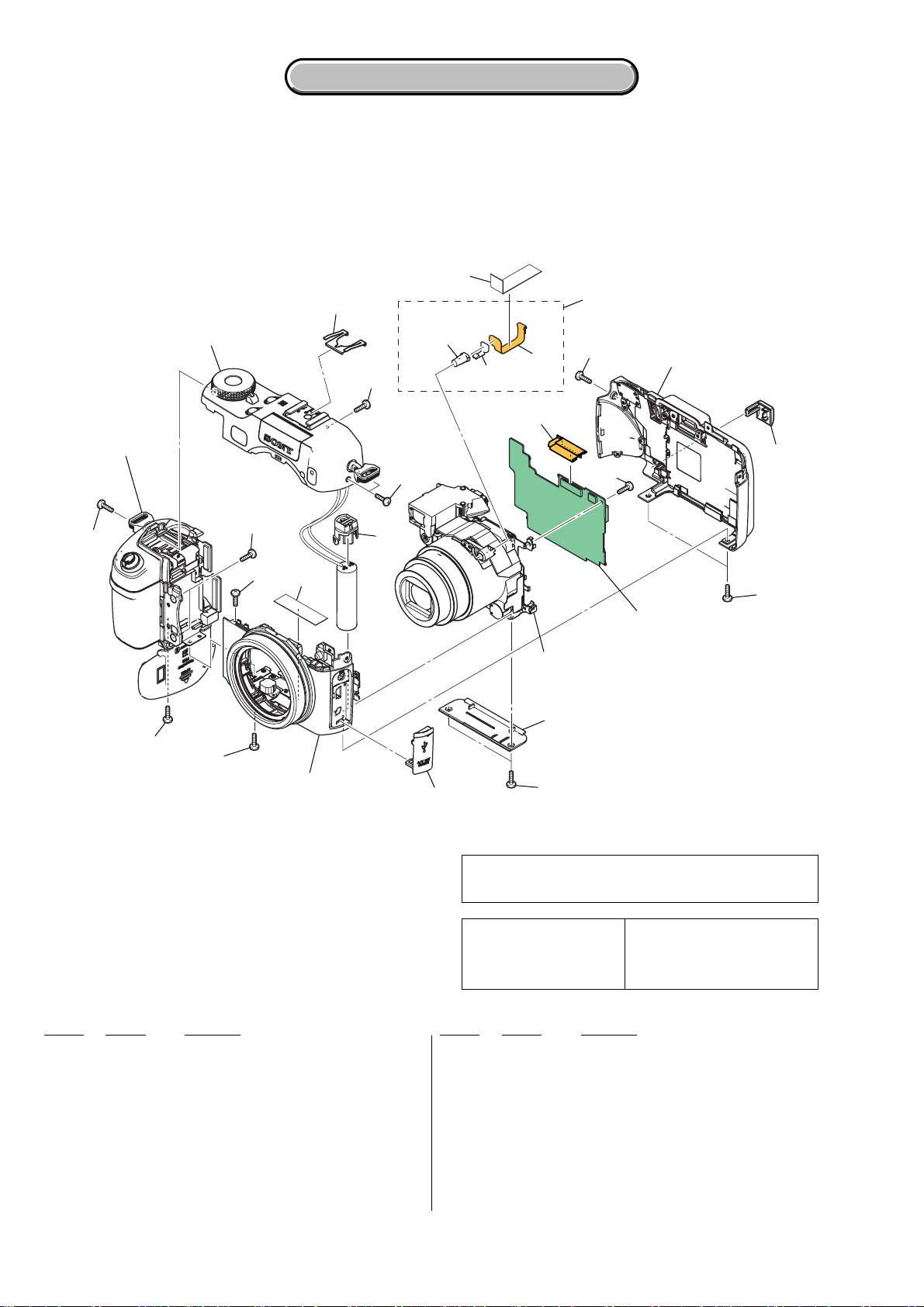
5-1. EXPLODED VIEWS
5-1-1. MAIN BLOCK
ns: not supplied
Cabinet (upper) block
(See page 5-6.)
5. REPAIR PARTS LIST
5. REPAIR PARTS LIST
4
D109
(Note)
1
7
8
ns
1
Cabinet (rear) block
(See page 5-7.)
9
Grip block
(See page 5-4.)
1
14
2
2
1
Cabinet (front) block
(See page 5-3.)
5
6
1
SY-106
12
3
7
1
13
(Includeing CP201
Lens block
(See page 5-5.)
(CH-146 board))
10
11
(Note) Be sure to read “PRECAUTIONS FOR USE OF LASER
1
UNIT” on page 1-2 when removing the laser unit and
AF-008 flexible board.
Ref. No. Part No. Description
1 2-515-756-91 SCREW (M1.7), TORASUTA, P2
2 3-080-222-11 SCREW (M1.7), TAPPING, P2
3 2-187-067-01 COVER, CAPACITOR
4 3-082-835-01 SPRING, SHOE
5 1-864-458-11 FP-082 FLEXIBLE BOARD
6 2-187-068-01 COVER, DC
7 3-941-343-21 TAPE (A)
0 8 A-1077-533-A AF-008 FLEXIBLE BOARD, COMPLETE (Note)
9 3-083-456-01 RETAINER, ASSIST LIGHT COVER
10 2-187-069-01 BOTTOM, CABINET
DSC-V3
The components identified by
mark 0 or dotted line with
mark 0 are critical for safety.
Replace only with part number specified.
Ref. No. Part No. Description
11 2-187-070-01 LID, JK
12 3-080-222-21 SCREW (M1.7), TAPPING, P2
13 A-1085-167-A SY-106 BOARD, COMPLETE
13 A-1089-920-A SY-106 BOARD, COMPLETE
14 3-989-735-51 SCREW (M1.7), LOCK ACE, P2
0 D109 1-805-470-01 LASER UNIT (Note)
(Including CP201 (CH-146 board)) (SERVICE) (J)
Les composants identifiés par une
marque 0 sont critiques pour la
sécurité.
Ne les remplacer que par une pièce
portant le numéro spécifié.
(Including CP201 (CH-146 board))
5-2
(SERVICE) (EXCEPT J)
Page 48

5-1-2. CABINET (FRONT) BLOCK
ns: not supplied
5. REPAIR PARTS LIST
5. REPAIR PARTS LIST
57
52
ns
SP901
56
54
55
54
JK-269
57
58
54
59
53
51
Ref. No. Part No. Description
51 X-2023-600-1 CABINET (FRONT) ASSY
52 X-2025-229-1 RING ASSY (SERVICE USE), LENS
53 2-187-015-01 PLATE, JK GROUND
54 2-025-236-31 SCREW (M1.7 )
55 2-187-017-01 PLATE, LENS GROUND
ns
Ref. No. Part No. Description
56 2-186-686-01 RETAINER, SPEAKER
57 3-080-222-11 SCREW (M1.7), TAPPING, P2
58 A-1077-525-A JK-269 FLEXIBLE BOARD, COMPLETE
59 2-187-018-01 SLIDER, DETECTION (SW)
SP901 1-825-262-31 LOUD SPEAKER (1.6CM)
DSC-V3
5-3
Page 49

5-1-3. GRIP BLOCK
ns: not supplied
5. REPAIR PARTS LIST
5. REPAIR PARTS LIST
102
101
103
104
117
ns
105
CF-099
116
105
107
ns
115
(Note)
106
ns
ns
BT001
112
108
109
110
DD-217
!
111
118
(Note) If it is original the battery lid can’t be disassembled.
Be sure to read “DISASSEMBLY” (page 2-2) when removing the battery lid.
CAUTION
Danger of explosion if battery is incorrectly replaced.
Replace only with the same or equivalent type.
Ref. No. Part No. Description
101 X-2023-598-1 GRIP ASSY
102 2-187-080-01 RUBBER (FRONT)
103 2-187-086-01 CEMENT (GRIP RUBBER), CONTACT
104 2-187-081-01 SHEET METAL (L), STRAP BRACKET
105 3-078-890-21 SCREW, TAPPING
106 3-087-116-01 BRACKET (FRONT), STRAP
107 A-1077-529-A RE-003 FLEXIBLE BOARD, COMPLETE
108 A-1077-531-A BT-026 FLEXIBLE BOARD, COMPLETE
109 A-1077-527-A BB-005 FLEXIBLE BOARD, COMPLETE
110 3-080-222-11 SCREW (M1.7), TAPPING, P2
114
113
!
BT001(BATTERY, LITHIUM SECONDARY)
Board on the mount position (See page 4-66)
The components identified by
mark 0 or dotted line with
mark 0 are critical for safety.
Replace only with part number specified.
Ref. No. Part No. Description
111 A-1077-521-A DD-217 BOARD, COMPLETE
112 A-1077-532-A LI-072 FLEXIBLE BOARD, COMPLETE
113 2-186-859-01 FOOT, RUBBER
114 X-2023-601-1 HOLDER ASSY, BATTERY
115 2-186-864-01 LID, BATTERY
116 A-1077-526-A MS-211 FLEXIBLE BOARD, COMPLETE
117 3-078-889-51 SCREW (M1.7)
118 A-1077-522-A CF-099 BOARD, COMPLETE
0 BT001 1-528-999-61 BATTERY, LITHIUM SECONDARY
Les composants identifiés par une
marque 0 sont critiques pour la
sécurité.
Ne les remplacer que par une pièce
portant le numéro spécifié.
DSC-V3
5-4
Page 50

5-1-4. LENS BLOCK
ns: not supplied
5. REPAIR PARTS LIST
5. REPAIR PARTS LIST
157
158
151
152
158
155
IC101
(Note 1, 2)
154
153
CD-515
160
ns
158
156
159
DSC-V3
Ref. No. Part No. Description
151 A-1079-957-A LENS ASSY (B158C)
152 2-188-926-01 SHEET (LE), ABSORBING
153 3-054-555-01 RUBBER (K), SEAL
154 1-788-183-11 OPTICAL FILTERBLOCK (OFB-02-20)
155 A-1077-528-A CD-515 FLEXIBLE BOARD, COMPLETE
156 3-078-890-21 SCREW, TAPPING
(Note 1) IC101 is not included in CD-515 flexible complete board.
(Note 2) Be sure to read “Precuations for Replacement of CCD
Imager” on page 4-8 when changing the CCD imager.
Ref. No. Part No. Description
157 2-187-010-01 FRAME, LENS
158 3-080-222-11 SCREW (M1.7), TAPPING, P2
159 2-187-013-01 PLATE, SY GROUND
160 2-187-012-01 HOLDER, LASER
IC101 A-1076-017-A CCD BLOCK ASSY (CCD IMAGER) (Note 1, 2)
5-5
Page 51
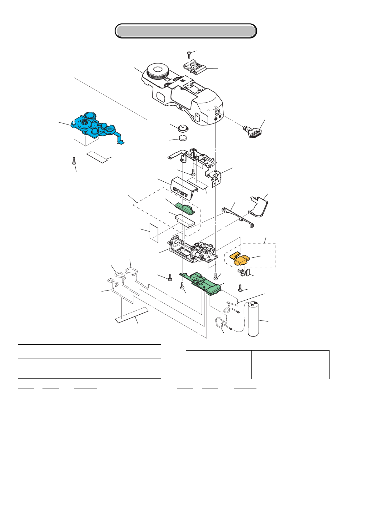
5. REPAIR PARTS LIST
)
5. REPAIR PARTS LIST
201
5-1-5. CABINET (UPPER) BLOCK
ns: not supplied
206
207
208
203
212
227
MIC901
211
213
205
ns
210
207
202
204
209
214
215
216
222
(Note 2)
224
(Note 2)
223
(Note 2)
207
(Note 1) C205 is not included in ST-111 complete board.
(Note 2) Be sure to read “2-3. THE METHOD OF ATTA CHMENT
Ref. No. Part No. Description
OF HARNESSES” (page 2-7) when removing the harness.
201 3-057-082-21 SCREW (M1.7), P2
202 1-817-518-11 SHOE CONNECTOR
203 X-2023-599-1 CABINET (UPPER) ASSY
204 3-087-116-01 BRACKET (FRONT), STRAP
205 2-187-075-01 CUSHION, MICROPHONE
225
208
226
201
221
201
217
218
219
(Note 2)
C205 (Note 1
220
(Note 2)
The components identified by
mark 0 or dotted line with
mark 0 are critical for safety.
Replace only with part number specified.
Ref. No. Part No. Description
215 2-187-076-01 BLIND, ST
216 A-1077-530-A PL-001 FLEXIBLE BOARD, COMPLETE
217 2-187-099-01 PLATE, FIXED
218 3-078-890-21 SCREW, TAPPING
219 1-963-221-21 HARNESS (HN-002) (BLACK)
Les composants identifiés par une
marque 0 sont critiques pour la
sécurité.
Ne les remplacer que par une pièce
portant le numéro spécifié.
206 1-478-981-11 SWITCH BLOCK, CONTROL (SW51610)
207 3-914-343-21 TAPE (A)
208 3-080-222-11 SCREW (M1.7), TAPPING, P2
209 2-187-074-01 FRAME, SHOE
210 3-057-082-41 SCREW (M1.7), P2
211 X-2023-603-1 COVER ASSY, ST
0 212 A-1077-523-A FL-147 BOARD, COMPLETE
0 213 1-477-895-21 FLASH UNIT
214 2-187-077-01 COVER, HARNESS
DSC-V3
(MODE SW)
220 1-963-221-11 HARNESS (HN-002) (WHITE)
0 221 A-1077-524-A ST-111 BOARD, COMPLETE
222 1-963-220-21 HARNESS (HN-001) (BLUE)
223 1-963-220-31 HARNESS (HN-001) (PINK)
224 1-963-220-11 HARNESS (HN-001) (WHITE)
225 X-2023-602-1 CASE ASSY, ST
226 1-454-674-51 SOLENOID, PLUNGER
227 2-546-937-01 SHEET, ST ELECTROSTATIC
0 C205 1-100-542-21 CAP, ELECT 135uF 315V (Note)
MIC901 1-542-312-11 MICROPHONE
5-6
Page 52

5-1-6. CABINET (REAR) BLOCK
ns: not supplied
5. REPAIR PARTS LIST
5. REPAIR PARTS LIST
252
253
254
D901
255
256
ns
LCD901
DSC-V3
251
Ref. No. Part No. Description
251 2-188-793-01 SHEET, SY PROTECTION
252 3-080-222-11 SCREW (M1.7), TAPPING, P2
253 1-478-980-11 SWITCH BLOCK, CONTROL (SW51610)
254 2-187-006-01 RUBBER (REAR), GRIP
(REAR SW)
Ref. No. Part No. Description
255 2-188-797-01 SHEET (REAR), GRIP ADHESIVE
256 X-2023-597-1 CABINET (REAR) ASSY
D901 1-478-463-11 BLOCK, LIGHT GUIDE PLATE
LCD901 8-753-217-37 ACX326CM-J
5-7
Page 53

AF-008 BB-005 BT-026 CD-515 CF-099
5-2. ELECTRICAL PARTS LIST
Ref. No. Part No. Description Ref. No. Part No. Description
0 A-1077-533-A AF-008 FLEXIBLE BOARD, COMPLETE (Note)
******************************
3-083-456-01 RETAINER, ASSIST LIGHT COVER
< DIODE>
0 D109 1-805-470-01 LASER UNIT (Note)
A-1077-527-A BB-005 FLEXIBLE BOARD, COMPLETE
*******************************
< CONNECTOR>
CN301 1-778-594-21 CONNECTOR, BOARD TO
BOARD 80P
CN302 1-778-599-21 CONNECTOR, BOARD TO
BOARD 80P
A-1077-531-A BT-026 FLEXIBLE BOARD, COMPLETE
******************************
R116 1-216-864-11 SHORT CHIP 0
R117 1-216-864-11 SHORT CHIP 0
R118 1-216-829-11 METAL CHIP 4.7K 5% 1/10W
R119 1-216-803-11 METAL CHIP 33 5% 1/10W
A-1077-522-A CF-099 BOARD, COMPLETE
**********************
< CAPACITOR >
C101 1-107-826-11 CERAMIC CHIP 0.1uF 10% 16V
C102 1-107-826-11 CERAMIC CHIP 0.1uF 10% 16V
C103 1-100-662-11 TANTAL. CHIP 47uF 20% 6.3V
C105 1-107-826-11 CERAMIC CHIP 0.1uF 10% 16V
C106 1-119-750-11 TANTAL. CHIP 22uF 20% 6.3V
C107 1-125-777-11 CERAMIC CHIP 0.1uF 10% 10V
< CONNECTOR >
< BATTERY TERMINAL >
0BT001 1-780-061-11 BATTERY TERMINAL BOARD
A-1077-528-A CD-515 FLEXIBLE BOARD, COMPLETE
*******************************
(IC101 is not included in this complete board.)
< CAPACITOR >
C107 1-127-715-91 CERAMIC CHIP 0.22uF 10% 16V
C108 1-107-826-11 CERAMIC CHIP 0.1uF 10% 16V
C109 1-135-957-91 TANTAL. CHIP 10uF 20% 16V
C110 1-107-826-11 CERAMIC CHIP 0.1uF 10% 16V
< FERRITE BEAD >
FB101 1-414-921-11 INDUCTOR, FERRITE BEAD
< IC >
IC101 A-1076-017-A CCD BLOCK ASSY (CCD IMAGER) (Note)
< TRANSISTOR >
Q102 8-729-050-22 TRANSISTOR 2SC4250 (T5LSONY1)
Q103 8-729-037-74 TRANSISTOR UN9213J-(TX).SO
Q104 8-729-037-74 TRANSISTOR UN9213J-(TX).SO
Q105 8-729-037-74 TRANSISTOR UN9213J-(TX).SO
< RESISTOR >
R103 1-216-857-11 METAL CHIP 1M 5% 1/10W
R104 1-216-828-11 METAL CHIP 3.9K 5% 1/10W
R106 1-216-864-11 SHORT CHIP 0
R110 1-216-847-11 METAL CHIP 150K 5% 1/10W
R111 1-216-864-11 SHORT CHIP 0
R112 1-216-826-11 METAL CHIP 2.7K 5% 1/10W
R113 1-216-815-11 METAL CHIP 330 5% 1/10W
R114 1-216-864-11 SHORT CHIP 0
R115 1-216-864-11 SHORT CHIP 0
CN101 1-778-593-21 CONNECTOR, BOARD TO BOARD 60P
CN104 1-815-572-61 CONNECTOR, MEMORY STICK
CN105 1-818-801-21 PIN, CONNECTOR 50P (CF CARD)
< DIODE >
D102 6-500-813-01 DIODE MA2SD32008S0
D103 8-719-056-23 DIODE MA2S111-(K8).SO
D104 8-719-056-61 DIODE MAZS082008SO
D105 8-719-066-44 DIODE CL-270HR-C-TS
D106 8-719-056-23 DIODE MA2S111-(K8).SO
< COIL >
L101 1-469-549-21 INDUCTOR 1uH
< TRANSISTOR >
Q101 6-550-239-01 TRANSISTOR DTA144EMT2L
Q102 6-550-576-01 TRANSISTOR SSM6E01TU
< RESISTOR >
R102 1-218-937-11 RES-CHIP 47 5% 1/16W
R103 1-218-937-11 RES-CHIP 47 5% 1/16W
R104 1-218-990-11 SHORT CHIP 0
R105 1-218-937-11 RES-CHIP 47 5% 1/16W
R106 1-218-937-11 RES-CHIP 47 5% 1/16W
R107 1-218-937-11 RES-CHIP 47 5% 1/16W
R108 1-218-937-11 RES-CHIP 47 5% 1/16W
R109 1-218-937-11 RES-CHIP 47 5% 1/16W
R110 1-218-937-11 RES-CHIP 47 5% 1/16W
R111 1-218-937-11 RES-CHIP 47 5% 1/16W
R112 1-218-937-11 RES-CHIP 47 5% 1/16W
R113 1-218-937-11 RES-CHIP 47 5% 1/16W
R114 1-218-937-11 RES-CHIP 47 5% 1/16W
R115 1-218-957-11 RES-CHIP 2.2K 5% 1/16W
R116 1-218-937-11 RES-CHIP 47 5% 1/16W
R117 1-218-937-11 RES-CHIP 47 5% 1/16W
R118 1-218-937-11 RES-CHIP 47 5% 1/16W
DSC-V3
(Note) Be sure to read “SERVICE NOTE” on page 1-
2 when replacing the laser unit (D109).
(Note) Be sure to read “Precautions for Replacement
of CCD Imager” on page 4-8 when changing
the CCD imager.
5-8
The components identified by
mark 0 or dotted line with
mark 0 are critical for safety.
Replace only with part number specified.
Les composants identifiés par une
marque 0 sont critiques pour la
sécurité.
Ne les remplacer que par une pièce
portant le numéro spécifié.
Page 54

5-2. ELECTRICAL PARTS LIST
Ref. No. Part No. Description Ref. No. Part No. Description
R119 1-218-937-11 RES-CHIP 47 5% 1/16W
R120 1-218-937-11 RES-CHIP 47 5% 1/16W
R121 1-218-937-11 RES-CHIP 47 5% 1/16W
R122 1-218-937-11 RES-CHIP 47 5% 1/16W
R123 1-218-937-11 RES-CHIP 47 5% 1/16W
R124 1-218-937-11 RES-CHIP 47 5% 1/16W
R125 1-218-937-11 RES-CHIP 47 5% 1/16W
R126 1-218-937-11 RES-CHIP 47 5% 1/16W
R127 1-218-937-11 RES-CHIP 47 5% 1/16W
R128 1-218-981-11 RES-CHIP 220K 5% 1/16W
R129 1-218-959-11 RES-CHIP 3.3K 5% 1/16W
R130 1-216-864-11 SHORT CHIP 0
R131 1-216-864-11 SHORT CHIP 0
R132 1-218-948-11 RES-CHIP 390 5% 1/16W
< SWITCH >
S101 1-786-227-21 SWITCH, TACTILE (RESET)
Electrical parts list of the CH-146 and DD217 boards are not shown.
Pages 5-10 to 5-12 are not shown.
CF-099
DSC-V3
5-9
Page 55

FL-147 JK-269 LI-072 MS-211 PL-001 RE-003 ST-111
Ref. No. Part No. Description Ref. No. Part No. Description
0 A-1077-523-A FL-147 BOARD, COMPLETE
***********************
A-1077-530-A PL-001 FLEXIBLE BOARD, COMPLETE
*******************************
0 1-477-895-21 FLASH UNIT
< CAPACITOR >
0 C206 1-137-723-21 CERAMIC CHIP 0.047uF 10% 250V
< COIL >
0 L201 1-456-193-11 COIL, TRIGGER
< RESISTOR >
0 R210 1-216-121-11 RES-CHIP 1M 5% 1/10W
A-1077-525-A JK-269 FLEXIBLE BOARD, COMPLETE
******************************
< CONNECTOR >
0 CN101 1-794-962-11 CONNECTOR, SQUARE TYPE (USB 5P)
< DIODE >
D203 6-500-512-01 DIODE CL-330IRS-X-TU (IR EMITTER)
D204 8-719-077-09 DIODE CL-196HR-CD-T (SELF TIMER)
< FERRITE BEAD >
1-454-674-51 SOLENOID, PLUNGER
A-1077-529-A RE-003 FLEXIBLE BOARD, COMPLETE
*******************************
< SWITCH >
S001 1-786-602-11 SWITCH, TACTILE (SHUTTER)
0 A-1077-524-A ST-111 BOARD, COMPLETE
***********************
< CAPACITOR >
C001 1-164-943-11 CERAMIC CHIP 0.01uF 10% 16V
C201 1-137-710-11 CERAMIC CHIP 10uF 20% 6.3V
C203 1-127-715-91 CERAMIC CHIP 0.22uF 10% 16V
C204 1-107-826-11 CERAMIC CHIP 0.1uF 10% 16V
< CONNECTOR >
CN003 1-580-055-21 PIN, CONNECTOR (SMD) 2P
CN004 1-817-705-11 CONNECTOR, FPC (LIF (NON-ZIF).,) 10P
CN005 1-815-330-11 CONNECTOR, FPC (ZIF) 15P
CN006 1-817-623-41 CONNECTOR, FPC (ZIF) 45P
CN007 1-816-654-31 FFC/FPC CONNECTOR (LIF) 6P
DSC-V3
FB101 1-500-444-11 FERRITE, EMI (SMD) (1608)
FB103 1-469-179-21 INDUCTOR, FERRITE BEAD
FB106 1-469-179-21 INDUCTOR, FERRITE BEAD
FB107 1-500-284-21 INDUCTOR, FERRITE BEAD
FB108 1-500-284-21 INDUCTOR, FERRITE BEAD
< JACK >
J102 1-793-995-21 JACK, SUPER SMALL TYPE (ACC)
J103 1-793-620-41 JACK (A/V OUT (MONO))
< RESISTOR >
R101 1-216-864-11 SHORT CHIP 0
R206 1-216-817-11 METAL CHIP 470 5% 1/10W
< SWITCH >
S101 1-762-805-41 SWITCH, PUSH (1 KEY)
(LENS ADAPTOR DETECT)
A-1077-532-A LI-072 FLEXIBLE BOARD, COMPLETE
******************************
< BATTERY >
0 BT001 1-528-999-32 BATTERY, LITHIUM SECONDARY
A-1077-526-A MS-211 FLEXIBLE BOARD, COMPLETE
*******************************
< CONNECTOR >
CN001 1-778-593-21 CONNECTOR, BOARD TO BOARD 60P
CN002 1-778-598-21 CONNECTOR, BOARD TO BOARD 60P
< DIODE >
D004 6-500-776-01 DIODE MAZW068H0LS0
D005 6-500-776-01 DIODE MAZW068H0LS0
D006 8-719-123-76 THYRISTOR 03P4J-T1
D007 8-719-073-01 DIODE MA111-(K8).S0
D201 8-719-073-01 DIODE MA111-(K8).S0
0 D202 6-500-962-01 DIODE HAU160C030STP
< FERRITE BEAD >
FB001 1-500-284-21 INDUCTOR, FERRITE BEAD
FB002 1-469-581-21 INDUCTOR, FERRITE BEAD (1005)
FB003 1-400-354-11 INDUCTOR, FERRITE BEAD (1005)
< IC >
0 IC201 6-703-635-01 IC TND721MH5-S-TL-E
< TRANSISTOR >
0 Q201 6-550-759-01 TRANSISTOR CPH3235-S-TL-E
0 Q202 8-729-056-01 TRANSISTOR MCH3405-TL-E
0 Q203 6-550-891-01 TRANSISTOR GT8G133 (T2LSONY.Q)
< RESISTOR >
R002 1-218-953-11 RES-CHIP 1K 5% 1/16W
R003 1-218-990-11 SHORT CHIP 0
R202 1-218-962-11 RES-CHIP 5.6K 5% 1/16W
R203 1-218-977-11 RES-CHIP 100K 5% 1/16W
R204 1-218-956-11 RES-CHIP 1.8K 5% 1/16W
R205 1-218-965-11 RES-CHIP 10K 5% 1/16W
R206 1-218-961-11 RES-CHIP 4.7K 5% 1/16W
R207 1-218-950-11 RES-CHIP 560 5% 1/16W
5-13
The components identified by
mark 0 or dotted line with
mark 0 are critical for safety.
Replace only with part number specified.
Les composants identifiés par une
marque 0 sont critiques pour la
sécurité.
Ne les remplacer que par une pièce
portant le numéro spécifié.
Page 56

ST-111
Ref. No. Part No. Description Ref. No. Part No. Description
R208 1-218-937-11 RES-CHIP 47 5% 1/16W
R209 1-218-989-11 RES-CHIP 1M 5% 1/16W
< SWITCH >
S201 1-786-180-31 SWITCH, PUSH (1KEY)
< TRANSFORMER >
0T202 1-443-417-21 DC-DC CONVERTER TRANSFORMER
(STROBE POP UP DETECT)
Electrical parts list of the SY -106 board is not
shown.
Pages 5-15 to 5-18 are not shown.
DSC-V3
5-14
The components identified by
mark 0 or dotted line with
mark 0 are critical for safety.
Replace only with part number specified.
Les composants identifiés par une
marque 0 sont critiques pour la
sécurité.
Ne les remplacer que par une pièce
portant le numéro spécifié.
Page 57

Checking supplied accessories.
Power cord (1)
0 1-769-608-11 (AEP, E)
0 1-782-476-13 (CH)
0 1-783-374-11 (UK, HK)
0 1-790-107-22 (US, CND)
0 1-790-732-12 (JE, J)
0 1-823-947-11 (KR)
0 1-827-945-11 (AUS)
CD-ROM
(USB driver: SPVD-012) (1)
2-187-477-01 (US, J)
2-187-478-01 (EXCEPT US, J)
USB cable (1)
1-827-038-11
AC-LS5/LS5B AC adaptor (1)
0 1-477-730-51
CD-ROM
(Image Data Converter Ver.2.0) (1)
2-514-710-01
Battery case (1)
(not supplied)
NP-FR1 battery pack (1)
(not supplied)
Shoulder strap (1)
3-071-638-12
Other accessories
2-318-592-01 MANUAL, INSTRUCTION (for BASIC)
2-318-592-11 MANUAL, INSTRUCTION (ENGLISH)
(EXCEPT AEP, KR, CH, J)
2-318-592-21 MANUAL, INSTRUCTION (FRENCH, ITALIAN)
2-318-592-31 MANUAL, INSTRUCTION
(SPANISH, PORTUGUESE) (AEP, E, JE)
2-318-592-41 MANUAL, INSTRUCTION (GERMAN, DUTCH)
2-318-592-51 MANUAL, INSTRUCTION
TRADITIONAL CHINESE)
2-318-592-61 MANUAL, INSTRUCTION
2-318-592-71 MANUAL, INSTRUCTION (ARABIC, PERSIAN)
2-318-592-81 MANUAL, INSTRUCTION (KOREAN) (KR, JE)
2-318-592-91 MANUAL, INSTRUCTION (CZECH, POLISH)
(JAPANESE) (J)
(CND, AEP)
(AEP)
(SIMPLIFIED CHINESE,
(E, HK, JE)
(RUSSIAN, SWEDISH)
(AEP)
(E)
(AEP)
DSC-V3
Conversion adaptor (1)
0 1-569-008-12 (E)
A/V connecting cable (1)
1-824-111-11
Conversion adaptor (1)
0 1-569-007-11 (E, JE)
2-318-593-01 MANUAL, INSTRUCTION (for APPLICATION)
2-318-594-11 MANUAL, INSTRUCTION
2-318-598-11 MANUAL, INSTRUCTION (ENGLISH) (CH)
2-318-598-21 MANUAL, INSTRUCTION
The components identified by
mark 0 or dotted line with
mark 0 are critical for safety.
Replace only with part number specified.
(HUNGARIAN, SLOVAKIAN) (AEP)
(SIMPLIFIED CHINESE,
TRADITIONAL CHINESE) (CH)
Les composants identifiés par une
marque 0 sont critiques pour la
sécurité.
Ne les remplacer que par une pièce
portant le numéro spécifié.
5-19E
(JAPANESE) (J)
Page 58

[Description of main button functions on toolbar of the Adobe Acrobat Reader Ver5.0 (for Windows)]
Toolbar
Printing a text
1. Click the Print button .
2. Specify a printer, print range, number of copies, and other options, and then click [OK].
Application of printing:
To set a range to be printed within a page, select the graphic
selection tool
be printed, and then click the Print button.
and drag on the page to enclose a range to
Finding a text
1. Click the Find button .
2. Enter a character string to be found into a text box, and click
the [Find]. (Specify the find options as necessary)
Application to the Service Manual:
To execute “find” from current page toward the pre vious pages,
select the check box “Find Backward” and then click the
“Find”.
3. Open the find dialog box again, and click the [Find Again] and
you can find the matched character strings displayed next.
(Character strings entered previously are displayed as they are
in the text box.)
Reversing the screens displayed once
•To reverse the previous screens (operation) one by one, click
.
the
•To advance the reversed screens (operation) one by one, click
.
the
Application to the Service Manual:
This function allows you to go and back between circuit diagram and printed circuit board diagram, and accordingly it
will be convenient for the voltage check.
Moving with link
1. Select either palm tool , zoom tool , text selection tool
, or graphic selection tool .
2. Place the pointer in the position in a text where the link exists
(such as a button on cover and the table of contents page, or
blue characters on the removal flowchart page or drawing
page), and the pointer will change to the forefinger form .
3. Then, click the link. (You will go to the link destination.)
Moving with bookmark:
Click an item (text) on the bookmark pallet, and you can move
to the link destination. Also, clicking can display the
hidden items.
(To go back to original state, click )
Application to the Service Manual:
The parts on the drawing pages (block diagrams, circuit diagrams, printed circuit boards) and parts list pages in a text
can be found using this find function. For example, find a
Ref. No. of IC on the block diagram, and click the [Find Again]
continuously, so that you can move to the Ref. No. of IC on
the circuit diagram or printed circuit board diagram successively.
Note: The find function may not be applied to the Service
Manual depending on the date of issue.
Switching a page
•To move to the first page, click the .
•To move to the last page, click the
•To move to the previous page, click the
•To move to the next page, click the
.
.
.
Zooming or rotating the screen display
“Zoom in/out”
• Click the triangle button in the zoom control box to select the
display magnification. Or, you may click
ing in or out.
“Rotate”
• Click rotate tool , and the page then rotates 90 degrees each.
or for zoom-
Application to the Service Manual:
The printed circuit board diagram you see now can be changed
to the same direction as the set.
Page 59

Reverse
987676231.pdf
Revision History
Ver.
1.0
Date
2004.09
History
Official Release
Contents
—
S.M. Rev.
issued
—
DSC-V3
 Loading...