

Page 1
http://servis-manual.com/
Page 2
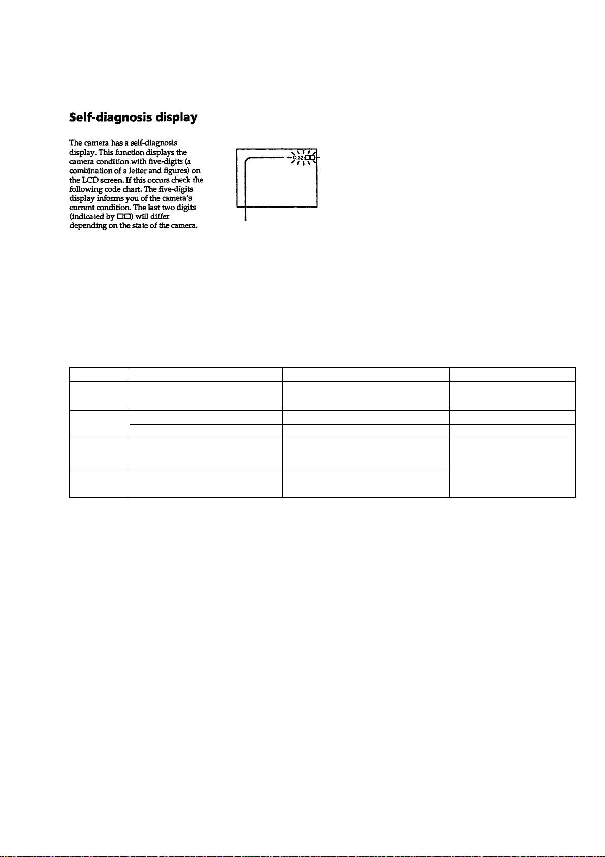
Self-diagnosis display
– If a code starting with an alp habet
letter appears
Your camera has a self-diagnosis display.
This function displays t he camera condit ion
on the LCD screen with a combination o f a
letter and four numerical digits. If this
occurs, check the f ollowing code chart and
attempt the co rresponding corrective
actions. The l as t two digits (indicated by
ss) will differ depending on the state of
the camera.
C:32:ss
Self-diagnosis display
Code Cause Corrective action
C:32: ss There is trouble with your
C:13: ss The camera cannot read or write
E:61: ss
E:91: ss
camera’s hardware.
data on the “Memory Stick.”
An unformatted “Memory Stick”
is inserted.
The inserted “Memory Stick”
cannot be used with your camera,
or the data is damaged.
A camera malfunction that you
cannot reverse has occurred.
Turn the power off and on again (page 14).
Re-insert the “Memory Stick” several
times.
Format the “Memory Stick” (pag e 37).
Insert a new “Memory Stick” (page 17).
Press the RESET button (page 97) located
on the bottom of the camera, then turn on
the power again.
If you are unable to solve the problem even
after trying th e corrective actions a few
times, contact your Sony dea ler or lo ca l
authorized Sony ser vice f acility and inf orm
them of the 5-digit code.
108
Page 3
1-5. DESCRIPTION ON SELF-DIAGNOSIS DISPLAY
Self-diagnosis display
• C: ss: ss
You can reverse the camera
malfunction yourself. (However,
contact your Sony dealer or local
authorized Sony service facility
when you cannot recover from the
camera malfunction.)
• E: ss: ss
Contact your Sony dealer or local
authorized Sony service facility.
DSC-V1
Display Code
C:32:ss
C:13:ss
E:61:ss
E:91:ss
Countermeasure
Turn the power off and on again.
Format the “Memory stick”.
Insert a new “Memory Stick”.
Checking of lens drive circuit.
Checking of flash unit or replacement
of flash unit.
Cause
Trouble with hardware.
Unformatted memory stick is inserted.
Memory stick is broken.
When failed in the focus and zoom
initialization.
Abnormality when flash is being
charged.
Caution Display During Error
SYSTEM ERROR
FORMAT ERR OR
MEMORY STICK ERROR
—
1-3E
Page 4

COVER
COVER
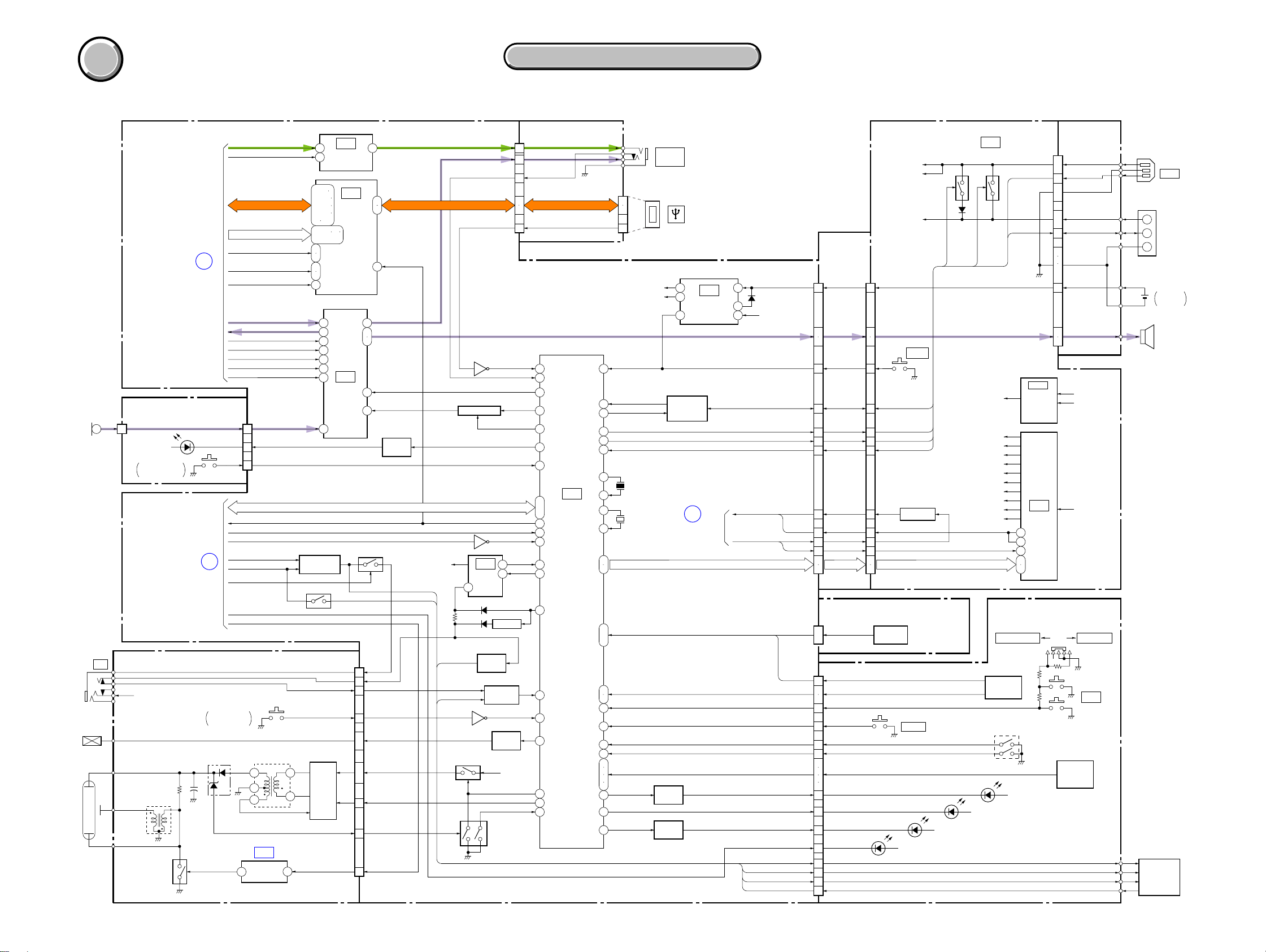
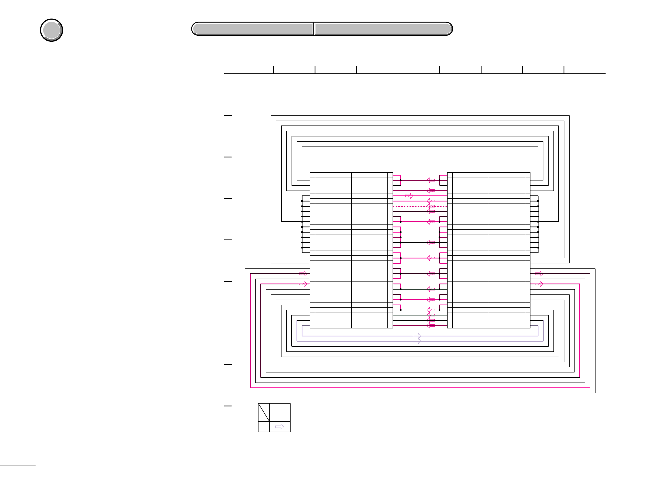
3. BLOCK DIAGRAMS
Link
Link
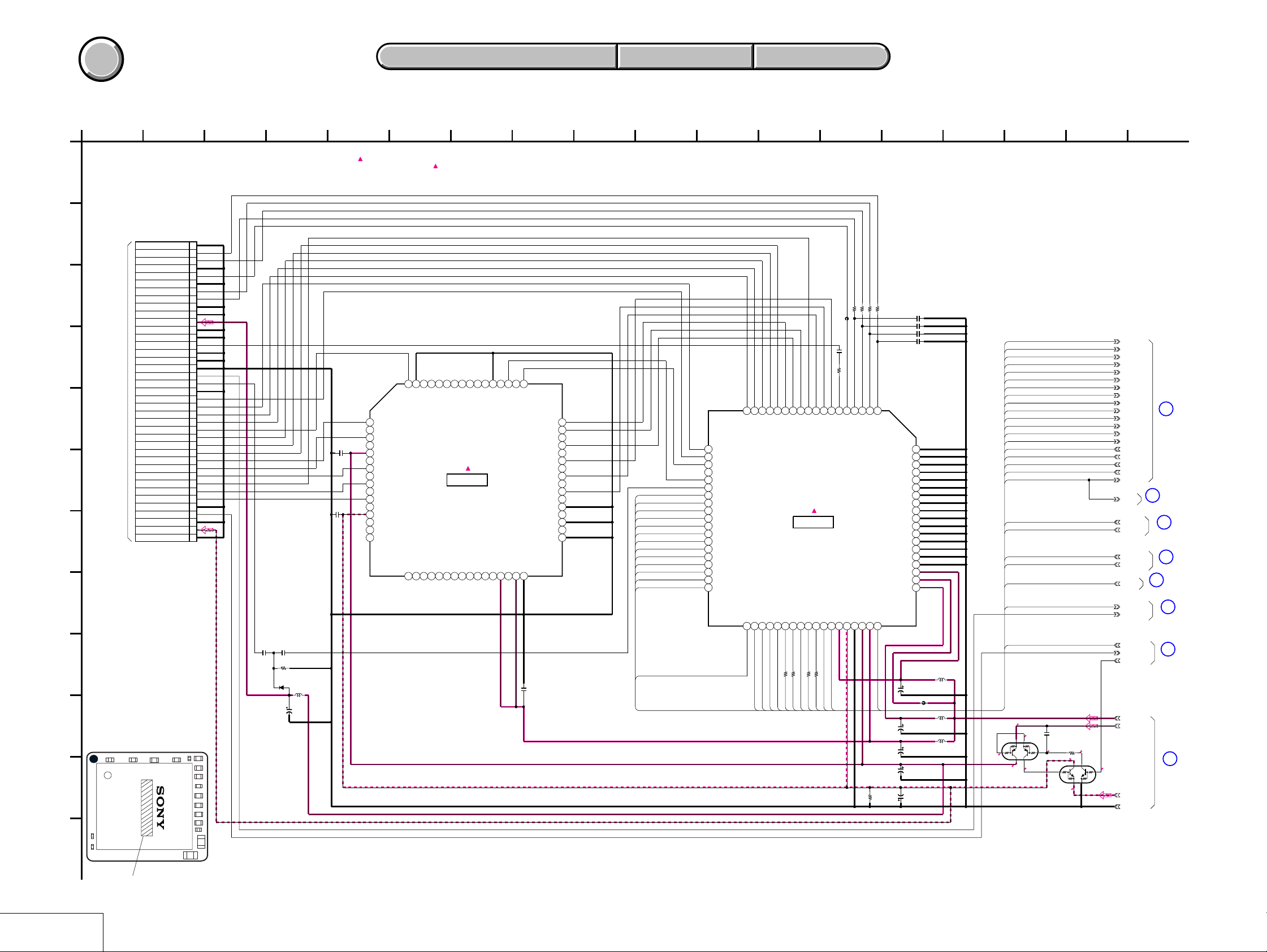
POWER BLOCK DIAGRAM (1/2)OVERALL BLOCK DIAGRAM (1/2)
POWER BLOCK DIAGRAM (1/2)OVERALL BLOCK DIAGRAM (1/2)
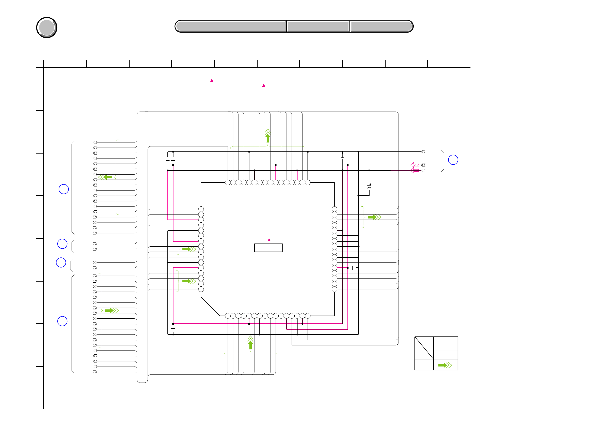
OVERALL BLOCK DIAGRAM (2/2) POWER BLOCK DIAGRAM (2/2)
OVERALL BLOCK DIAGRAM (2/2) POWER BLOCK DIAGRAM (2/2)
DSC-V1
Page 5
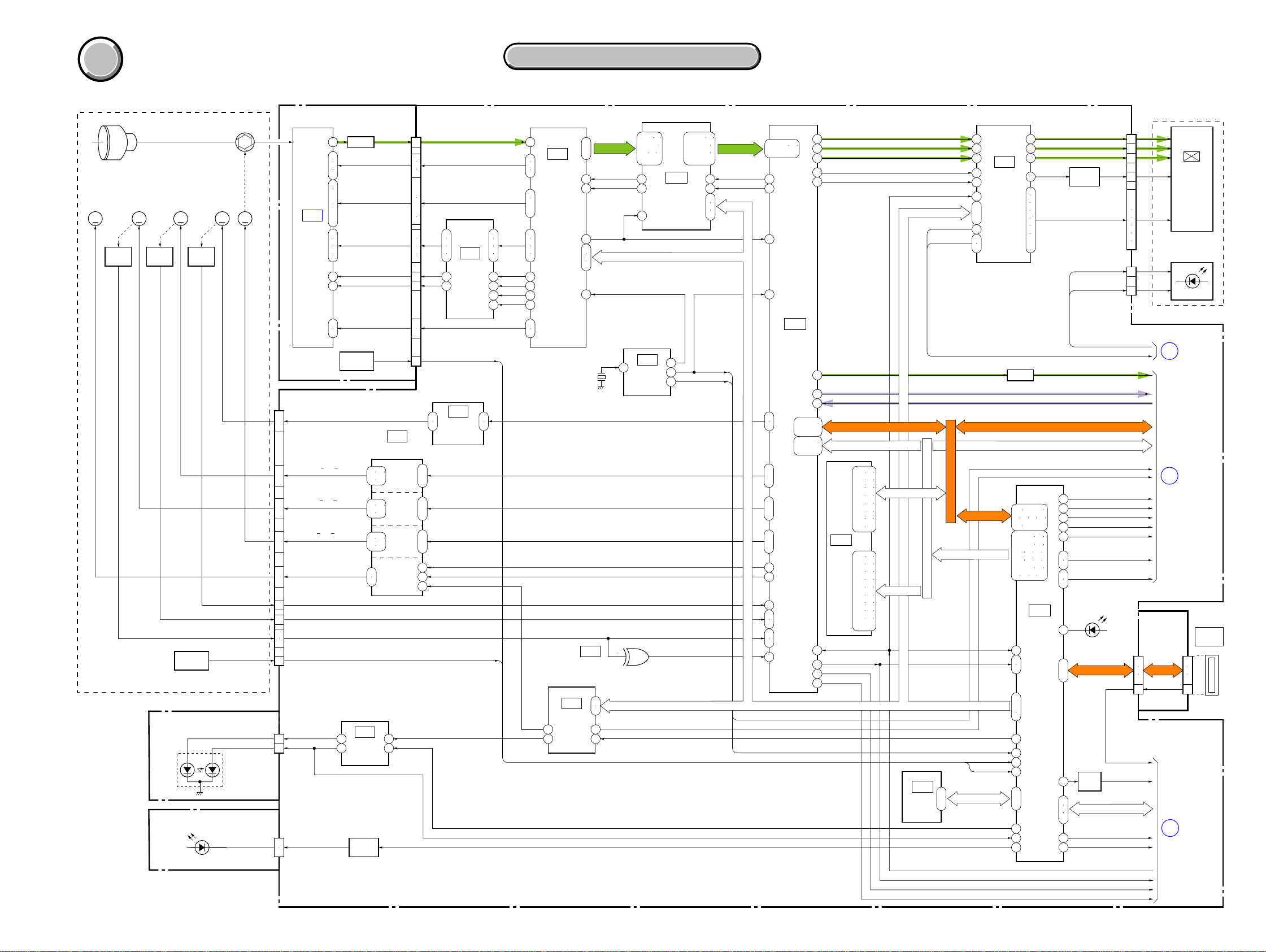
DSC-V1
COVER
COVER
SECTION 3
BLOCK DIAGRAMS
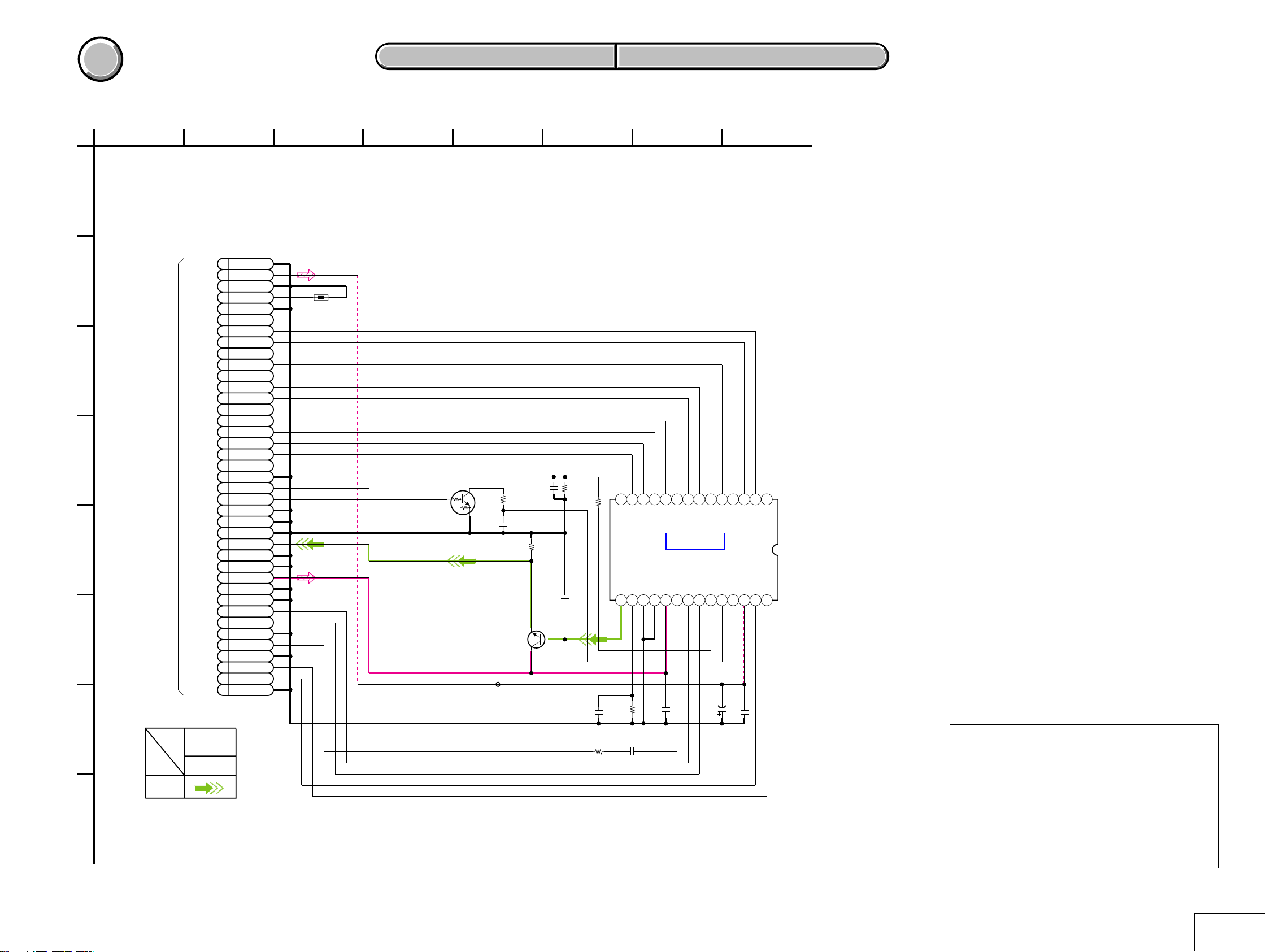
3-1. OVERALL BLOCK DIAGRAM (1/2)
LENS UNIT
LENS
ZOOM
SENSOR
ZOOM
MOTOR
M
FOCUS
SENSOR
SHUTTER
MOTOR
M
ST-083 FLEXIBLE BOARD (1/2)
SW-395 FLEXIBLE BOARD (1/2)
A : VIDEO SIGNAL
A : AUDIO SIGNAL
A : VIDEO/AUDIO SIGNAL
FOCUS
MOTOR
M
LENS TEMP
SENSOR
IR
SENSOR
IR FILTER
MOTOR
M
TEMP OUT
(LASER UNIT)
D101
(IR EMITTER)
IRIS
(SHUTTER)
MOTOR
M
LD OUT
PD OUT
D333
IR LED K
IRIS
CD-441 FLEXIBLE BOARD
IC101
CCD
IMAGER
CN301
1
IR FILTER±
ı
4
12
FOCUS A, A, B, B
ı
19
32
ZOOM A, A, B, B
ı
39
24
IRIS A, A, B, B
ı
27
20
SHUTTER±
ı
23
IR SENS RST
6
F RST SENS
8
28
Z RST SENS1, 2
29
10
CN751 (1/2)
25
27
CN753 (1/2)
5
6
05
3. BLOCK DIAGRAMS
3. BLOCK DIAGRAMS
( ) : Number in parenthesis ( ) indicates the division number of schematic diagram where the component is located.
SY-089 BOARD (1/2)
IC303
(3/12)
FOCUS
MOTOR
DRIVE
ZOOM
MOTOR
DRIVE
IRIS
MOTOR
DRIVE
SHUTTER
MOTOR
DRIVE
2
4
14
21
24
26
28
32
30
31
33
34
25
29
36
5
7
8
ı
ı
2
3
CN151
5
ı
8
1
ı
4
9
ı
12
47
48
31
3
7
9
IC151
11
V DRIVER
(1/12)
64
1
IC302
6
IR FILTER
7
MOTOR DRIVE
(3/12)
PRELAMP AF CONT
PRELAMP AF ON
PD LEV
2
3
LENS TEMP
XSG3A,
XSG3B,
XSG5A,
39
XSG5B
41
45
48
XV6
XV4
49
XV3
43
XV5
47 11
MSHUT REF
Q102
15 6
20
21
22
3
7
ı
9
11
ı
14
1
2
4
5
10
6
27
28
CCD TEMP
SENSOR
5
1
CCD OUT
BUFFER
RG, H1B, H2B
V2, V4, V5A, V5B,
V6, V7A, V7B, V8
V1A, V1B, V3A, V3B
Vhold
Vst
H1A, H2A
TH101
CCD TEMP CCD TEMP
LENS DRIVER
20 21
23 24
37 38
41 42
14 15
17 18
43
46
IC281
AF LASER
DRIVE
(11/12)
Q281
IR LED
DRIVE
IC152
5
2
CAMERA
4
MODULE
(1/12)
10
14
ı
20
8
9
12
13
2351
21
7
1
3
HR DIR0A, HR DIR0B
HR DIR1A, HR DIR1B
HR DIR2A, HR DIR2B
B1
A2
25
ı
38
46
47
MCK12
49
41
42
45
48
X581
27MHz
IR FILTER IN,
IR FILTER OUT
HR EN0,
HR EN1,
HR EN2,
MSHUT ON
MSHUT EN
XIR RST SENS
XFC RST SENS
XZM RST SENS1, 2
IC602
(4/12)
C4
IC304
B4
EVR
(D/A CONV.)
(3/12)
C1
A3
CA ADI00
ı
CA ADI13
TG CLK
1 - 4 6
8 - 10
56 57
61 - 64
CA HDI
CA FDI
CAM SO, XCAM SCK, XCAM RESET
2
GENERATOR
1 2 4
CAM SO, XCAM SCK
SP VOL
50
48
58
IC581
CLOCK
(6/12)
IC681
SIGNAL
GENERATOR,
SRAM
(2/12)
4
16
11
29 - 32 34
36 - 38
40 - 42
45 - 47
22
19
20
13
24
CKIO
USB CLK
CA AD00
ı
CA AD13
CA HD
CA FD
12 - 14 16
18 - 27
8
9
96
88
CAMERA DSP,
256M SDRAM
CAM SO, XCAM SCK, XCAM RESET
197
199
233
ı
235
237
ı
239
241
ı
243
246
196
185
192
232
187
184
248
USB CLK
IC601
(4/12)
65 - 69
71 - 81
29 - 41
43 - 54
212
207
204
225
229
215
278
272
94
227
249
248
MC A01 - A25
IC503
32M
FLASH
(6/12)
XRST SYS
SYS V
EXT STRB ON
STRB ON
PANEL R
PANEL G
PANEL B
HDO
PANEL V
XRST SYS
CAM SI, CAM SO, XCAM SCK
MC D00 - D15
C2 C3
C8 D7
D9 E1
MC D00 - D15
E4 E9
F2 F3
F7 F8
G2 G6
H2 J9
A3 A4
B3 B4
C4 D4
D6 G4
H3 H4
MC A01 - A21
H6 H7
J3 J4
J6 J7
K3 K4
K6 - K8
CAM SI, CAM SO, XCAM SCK, XCAM RESET
IC502
EEPROM
(6/12)
40
39
38
IC801
43
LCD DRIVE,
42
TIMING
GENERATOR
9
(7/12)
46
ı
BL ON
BL LEV
ADDRESS BUS MC A01 - A25
48
31
28
29
MC D00 - D15
DATA BUS MC D00 - D15
MC A01 - A25
XRST SYS
DAC STB
CCD TEMP
LENS TEMP
EEPROM,
SO, SI, SCK
2
ı
4
SYS V
CKIOCKIO
19
20
21
25
2
3
4
14
15
23
32
ı
35
Q606
BUFFER
MC D00 - D15
MC A01 - A07
39 41 - 45
47 49 51 52
54 56 - 60
62 - 64 66
68 - 70 72
73 75 76
78 79 81
83 - 88 90
92 93 95 97
IC501
MC CAM,
SH DSP,
FLASH
(5/12)
140
164
179
199
ı
201
220
19
187
230
229
202
ı
204
7
236
27 32
CN801
Q801, 802
RGT, HCK1, HCK2,
HST, WIDE, DWN,
EN, VCK, VST, COM
13
50
29
124
25
129
130
208
210
216
MS DIO, MS BS,
213
ı
215
35
185
190
191
17
PSIG
PSIG
DRIVE
CN702
BL THL
BL L
BL THL, BL L
BL ON, BL LEV
AU AOUT
XAU SP MUTE
XAU LINE MUTE
XAU POWER SAVE
XUSB DREQ0, XUSB DACK0
XUSB DREQ1, XUSB DACK1
D704
(MS ACCESS)
MS SCLK
Q501
XAE LOCK LED
LED
DRIVE
FR SI, FR SO, XFR SCK
EXT STRB CONT
EXT STRB ON
VR
21
VG
20
VB
22
19
2
ı
6
12
13
17
18
23
1
4
CV OUT
AU AINL
USB CLK
SP VOL
VAMP ON
AU HGL SEL
CN705
2
4
6
5
XMS IN
HSHOE CONT
XRST SYS
SYS V
STRB ON
PANEL UNIT
3
1
MS-165
FLEXIBLE
BOARD
DIO, BS,
SCLK
INT
2
LCD901
COLOR
LCD
MONITOR
D901
BACKLIGHT
OVERALL
(2/2)
(PAGE 3-4)
OVERALL
(2/2)
(PAGE 3-3)
MEMORY
STICK
8
4
2
6
OVERALL
(2/2)
(PAGE 3-3)
3-1 3-2
Page 6
DSC-V1
COVER
COVER
3. BLOCK DIAGRAMS
3. BLOCK DIAGRAMS
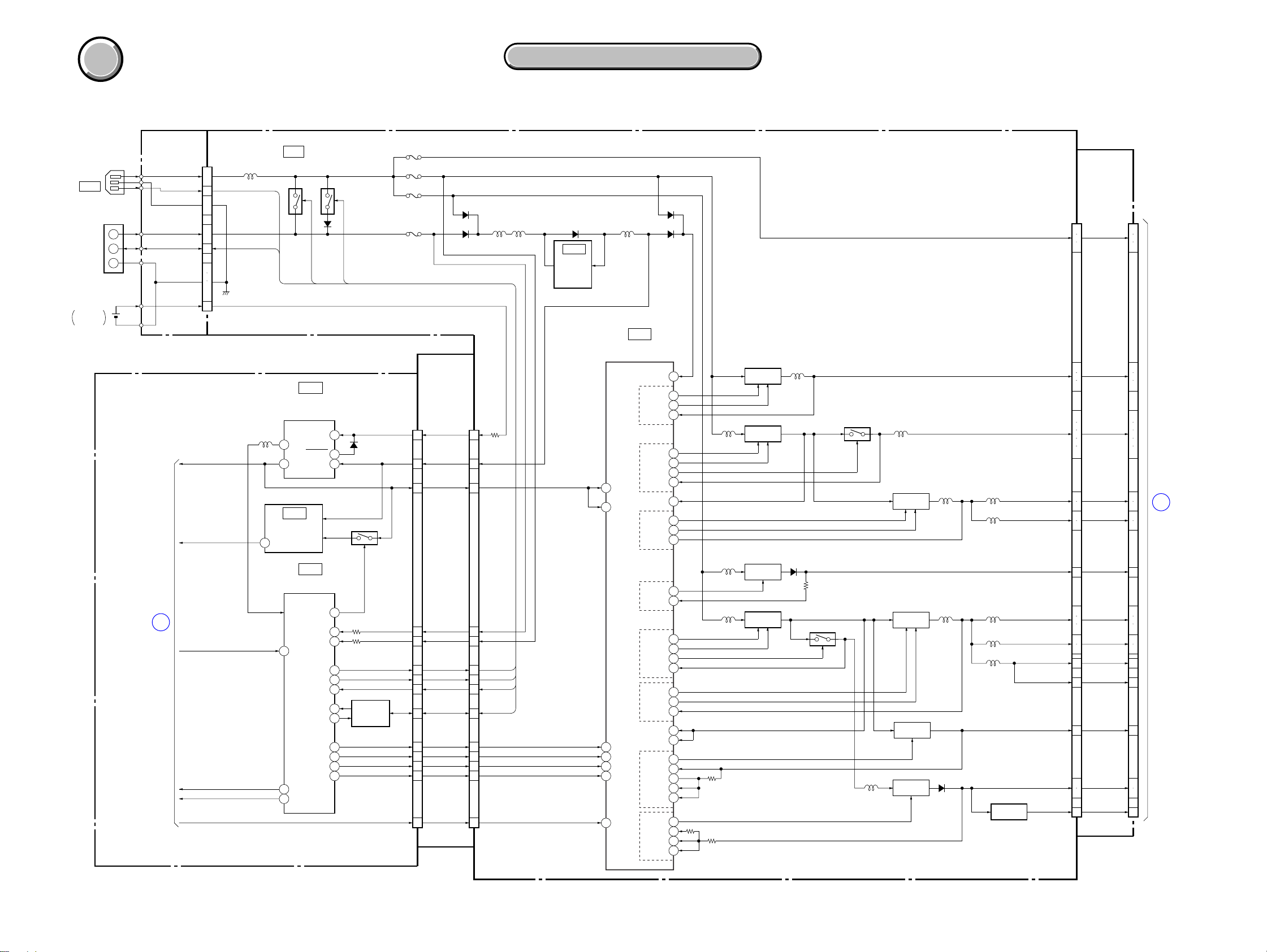
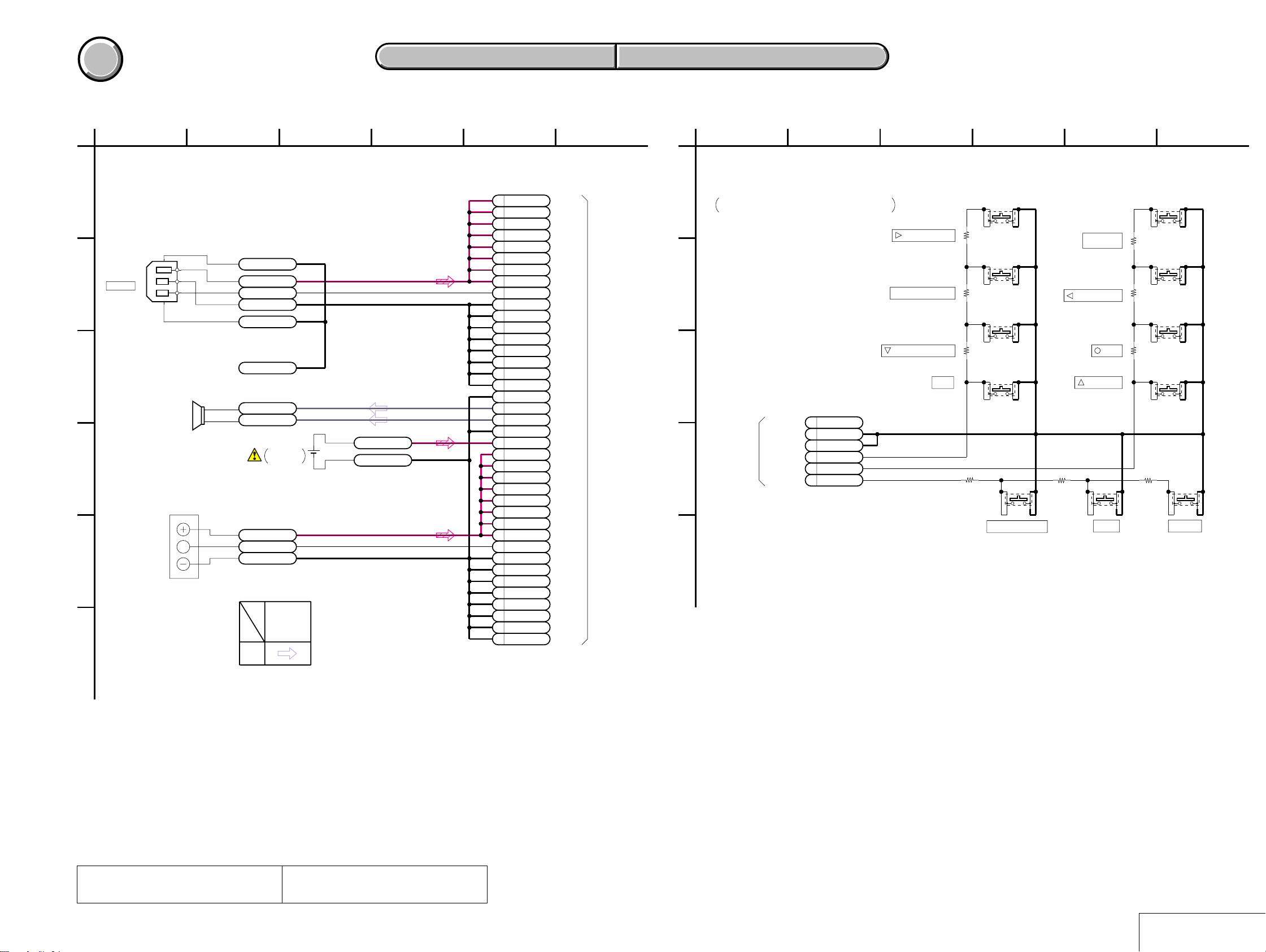
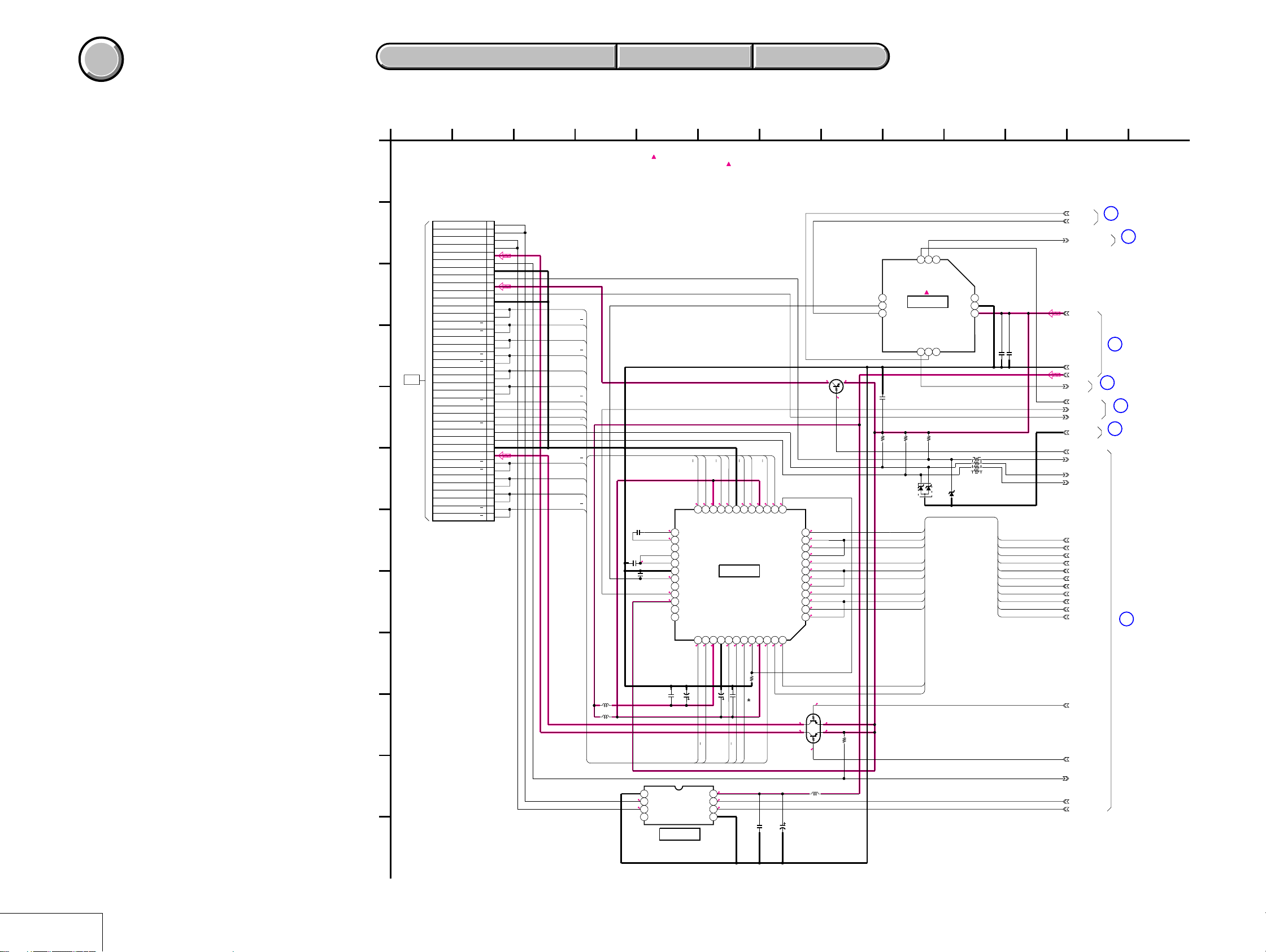
3-2. OVERALL BLOCK DIAGRAM (2/2)
SY-089 BOARD (2/2)
MIC901
MICROPHONE
J301
ACC
PLUNGER
FLASH
UNIT
05
OVERALL (1/2)
(PAGE 3-2)
1
SW-395 FLEXIBLE BOARD (2/2)
CN101
2
D102
(SELF TIMER)
S101
LENS ADAPTOR
DETECT
OVERALL (1/2)
(PAGE 3-2)
2
ST-083 FLEXIBLE BOARD (2/2)
LANC DC
STROBE OPEN
XE_H (Anode)
+
TRIGGER
XE L (Cathode)
L331
Q334
C333
CHARGING
CAPACITOR
CV OUT
VAMP ON
MC A01 - A07
XUSB DREQ0, XUSB DACK0
XUSB DREQ1, XUSB DACK1
USB CLK
AU AINL
AU AOUT
SP VOL
XAU SP MUTE
XAU LINE MUTE
AU HGL SEL
XAU POWER SAVE
CN753
(2/2)
10
8
2
SYS V
HSHOE CONT
EXT STRB ON
EXT STRB CONT
XAE LOCK LED
STRB ON
S301
DETECT
D332
5 1
4
3
IC331
FLASH
2
CONTROL
MIC SIG
XSELF TIMER LED
KEY AD4
T331
6
7
2 - 5
41 - 44
46 - 48
78 - 80
82 107
38 - 40 76
104 - 106
10
52
14
55
36
Q708
EXT STROBE
SWITCH
Q705, Q706
EXT1 STB ON
ACC XLANC JACK IN
Q331, Q332
TRANS
DRIVE
2
4
( ) : Number in parenthesis ( ) indicates the division number of schematic diagram where the component is located.
JK-254 FLEXIBLE BOARD
VIDEO AMP
H4
H5
J3
B2
C8
G8
H9
AUDIO AMP
B8
LANC SIG
IC101
4
(8/12)
IC901
97
USB
INTERFACE
IC201
(8/12)
99
(9/12)
35
B4
A2
D1
BEEP ON
F2 49
E1
Q406 (1/2)
Q703
CN751
(2/2)
32
30
33
XSTRB POPUP
28
37
STRB PLUNGER
ı
39
7
ST UNREG
ı
12
XSTRB PWRSAVE
5
STB FULL
1
STRB ON
4
XRST SYS
BEEP
LED
DRIVE
INTE STRB ON
USB D±MC D00 - D15
LANC DC
HOT
FR SI, FR SO, XFR SCKFR SI, FR SO, XFR SCK
INTE
SALA SIG
LANC JACK IN2
AU OUT
AV JACK IN
USB JACK IN
Q402 (1/2)
Q407
MODULATOR
Q403
IC401
LANC
DRIVER
11
(10/12)
D401
D405
LANC SIG
Q701, Q702
Q405, Q411 (1/2), Q412
Q411
(2/2)
Q753,Q754
CN752
V OUT
USB JACK IN
AV JACK IN
SELF TIMER LED
KEY AD4
XRST SYSXRST SYS
SYS V
MS INXMS IN
LANC IN
10
12
LANC OUT
XLANC PWR ON
Q409, Q410
SWITCH
LANC SIG
SWITCH
LANC JACK
INDETECT
Q751
PLUNGER
DRIVE
ST UNREG
STB CHARGE
XSTRB PWR SAVE
XSTB FULL
Q752
13
9
11
2
3
5
V OUT
AU OUT
AV JACK IN
USB JACK IN
9
11
74
79
19
59
23
ı
25
CONTROLLER
77
32
6
39
40
7
10
45
78
46
75
34
USB D±
IC402
FRONT
(10/12)
CN201
2
3
VCC
1
BACKUP VCC
XRESET
73
BATT SI
43
BATT SO
42
INIT CHARGE
47
FAST CHARGE
48
BATT/XEXT
8
29
10MHz
28
51
32.768kHz
52
20
21
55
KEY AD0 - AD2
ı
57
37
38
KEY AD3
58
XPWR ON
1
XSHTR ON
4
XAE LOCK SW
5
2
XPB ON, MODE DIAL2, MODE DIAL, XSETUP ON
35
54
60
17
15
16
EVER 3.0V
X401
X402
J201
A/V OUT
(MONO)
(USB)
6
8
INITIAL RESET,
BACK UP VCC
5
(10/12)
Q408
BATTERY
CHARGE
DETECTOR
3
OVERALL (1/2)
(PAGE 3-2)
UNREG SO, UNREG SCK UNREG SO, UNREG SCK
Q402 (2/2)
LED
DRIVE
Q406 (2/2)
LED
DRIVE
A : VIDEO SIGNAL
A : AUDIO SIGNAL
A : VIDEO/AUDIO SIGNAL
IC403
3
D403
2
7
BL THL, BL L BL THL
BL ON, BL LEV
Program Dial A, B
INTE SALA SIG
INTE STRB ON
LANC JACK IN2
LANC 5.5V
SP ±
BL L
BL LEV
BL ON
KEY AD0 - AD2
KEY AD2
KEY AD3
XPWR ON
XSHTR ON
XAE LOCK ON
PWR LED ON
XTALLY LED
XCHARGE LED
AE LOCK LED
CN703
CN704
DD-195 BOARD
IC002
, Q001
Q004, Q005
D004
INIT CHARGE
S081
Q002
BB-004
FLEXIBLE
BOARD
58
60
XRESET FR
BATT SIG
INIT CHARGE
FAST CHARGE
BATT/XEXT
BL LEVEL
4
DATA, CLK
8
SP ±
BL THL
BL L
BL ON
ACV UNREG
ST UNREG
BATT UNREG
CN402 CN082CN401CN701
58
60
RESET
5454
4848
5050
5252
4646
4242
3838
3636
3434
4
8
BATT SIG
INIT CHARGE
FAST CHARGE
BATT/XEXT
SWITCHING
CONTROL SWITCH BLOCK (GL-51470)
4
ı
6
22
23
24
9
15
2
1
10
11
13
14
16
18
21
19
LANC SIG
4
HOTHOT HOT
6
INTE STRB ON
7
LANC JACK IN2
8
S251 - S261
FUNCTION
KEY
EXECUTE
DIAL A, BDIAL A, B
S104
POWER
XSHTR ON
XAE LOCK ON
XPB ON, MODE DIAL2, MODE DIAL, XSETUP ON
D108
(FLASH/CHG)
D107
(AE/AF LOCK)
SWITCH
(1/2)
BATT/XEXT
BATT SIG
FAST CHARGE
IC003
,
S103
CONVERTER
CONTROL
59
60
48
45
46
D105
(POWER)
Q019
DC/DC
(1/2)
IC001
(2/2)
LANC 5.5V
D 1.5V
D 2.9V
A 2.9V
PANEL 2.9V
CAM 3.2V
USB 3.2V
CAM P 5V
CAM 15V
CAM –7.5V
PANEL 13.5V
CONTROL SWITCH BLOCK
(MODE-51470)
NIGHTFRAMING NIGHTSHOT
S106
JOG DIAL
(SHUTTER)
D106
(SELF TIMER/RECORDING)
CN081
DC
10
17
23
30
31
18
21
32
39
225959
19
20
S102
(OFF)
1
ı
8
9
ı
ı
ı
FU-165
FLEXIBLE
BOARD
ACV UNREG1
BATT UNREG1
S108
MODE
LANC JACK IN2
BATT/XEXT1
ACV GND1
BATT SIG1
BATT GND1
VL 3VVL 3V
SP ±SP ±
BATT UNREG
ACV UNREG
ACV UNREG
S105
(UP)
ZOOM
S101
(DOWN)
DIAL
LANC SIG
INTE STRB ON
J101
DC IN
+
BT901
S
BATTERY
TERMINAL
−
BT101
LITHIUM
BATTERY
SP901
SPEAKER
INTTELLIGENT
SHOE
3-3 3-4
Page 7
COVER
COVER
3. BLOCK DIAGRAMS
3. BLOCK DIAGRAMS
DSC-V1
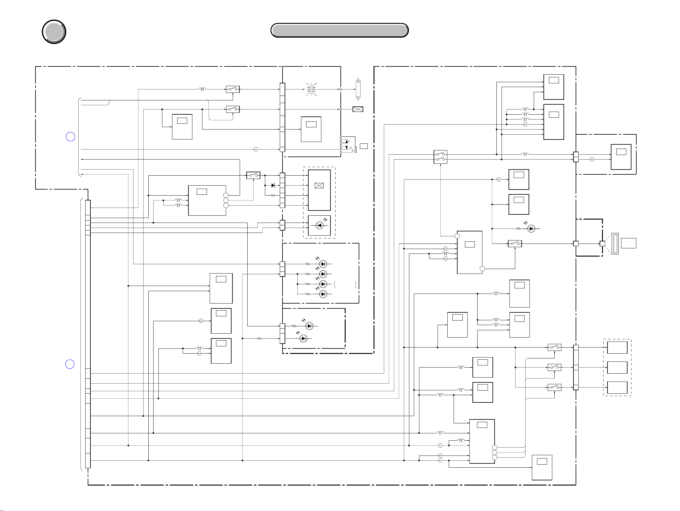
3-3. POWER BLOCK DIAGRAM (1/2)
DD-195 BOARD
CN081
1
ı
8
9
10
ı
17
23
ı
30
31
18
21
32
ı
39
22
EVER 3.0V
LANC DC
D 1.5V
STB PLUNGER
STB CHARGE
BL ON
LF001
BATT/XEXT
BATT SIG
L401
14
BACKUP
IC002
SWITCH
(1/2)
INITIAL RESET,
BACK UP VCC
VOUT
6
VRO
8
IC401
LANC DRIVER
(10/12)
LANC DC
FRONT CONTROLLER
VCC
66 DD CON SENS
FAST CHARGE
INIT CHARGE
BATT/XEXT
SYS DD ON
XCS DDCON
UNREG SO
UNREG SCK
78 STB PLUNGER
46 STB CHG
(10/12)
(10/12)
ACV SENS
J101
DC IN
BT901
BATTERY
TERMINAL
BT101
LITHIUM
BATTERY
SY-089 BOARD (1/2)
(PAGE 3-7)
05
+
S
−
POWER 2
FU-165
FLEXIBLE
BOARD
ACV UNREG1
BATT/XEXT1
ACV GND1
BATT UNREG1
BATT SIG1
BATT GND1
VL 3V
A
( ) : Number in parenthesis ( ) indicates the division number of schematic diagram where the component is located.
, Q001
D004
FAST CHARGE
IC403
VBAT
PREEND
VIN
IC402
BATT SI
BATT SO
Q004, Q005
INIT CHARGE
VL 3V
3
2
7
LANC 5.5V
18XLANC ON
67BATT SENS
68
48
47
8
43
42
76
22
20
21
CHARGE
CONTROL
D403
Q401
Q408
BATTERY
CHARGE
DETECTOR
F001
F002
F004
F006
BB-004
FLEXIBLE
BOARD
(1/2)
CN401
CN701
(1/2)
(1/2)
59
7
9
BATT UNREG
57 57
ACV UNREG
55 55
FAST CHARGE
52 52
INIT CHARGE
50 50
BATT/XEXT
46 46
48 48
SYS DD ON
2
6
8
4
34
D009
D010
CN402
(1/2)
VL 3V
LANC 5.5V
EVER 3.0VEVER 3.0V
BATT SIG
XCS
DATA
CLK
BL ON BL ON
L018 L006
ACV UNREG
BATT UNREG
CN082
(1/2)
59
7
9
2
6
8
4
34
VL 3V
LANC 5.5V
ACV UNREG
BATT UNREG
DC/DC
CONVERTER
EVER 3.0V
SYS DD ON
XCS DDCON
UNREG SO
UNREG SCK
D011
IC003
,
Q019
(1/2)
LANC 5.5V
56
VCC1
47
RST
57
CONT
44
XCS
45
DATA
46
CLK
48
ONOFF2
L010
IC001
DC CONTROL
(2/2)
AMPOUT
VCC2
OUT1p
OUT1n
VIN1–
OUT6p
OUT6n
OUT6S
VIN6–
VCC4
OUT4p
OUT4n
VIN4–
OUT2n
OVP2
OUT5p
OUT5n
OUT5S
VIN5–
OUT3p
OUT3n
VIN3–
VCC3
VCC5
OUT10
AMPIN
IN10
FB10
OUT9
FB9
IN9–
SCP9
D008
D012
−
Q011, Q015
L003
L001
L002
SWITCHING
Q008, Q018
SWITCHING
Q023
SWITCHING
Q007, Q017
SWITCHING
41
36
37
55
28
29
18
50
19
30
31
53
35
58
38
39
43
52
32
33
54
42
20
22
4
5
3
2
23
79
80
1
L007
D015
Q020 (2/2)
Q020 (1/2)
L004
L017
Q010, Q014
SWITCHING
Q012, Q016
SWITCHING
Q009
SWITCHING
Q024
SWITCHING
L009
L008
D014
L015
L016
L012
L013
L014
Q021, Q022
13.5V REG
CN082
ST UNREG
D 1.5V
CAM P 5V
CAM 3.2V
USB 3.2V
BL H
D 2.9V
A 2.9V
PANEL 2.9V
BL THH
CAM –7.5V
CAM 15V
PANEL 13.5V
(2/2)
BB-004
FLEXIBLE
BOARD
(2/2)
CN402
(2/2)
1
3
5
31
33
35
21
23
25
27
29
47
49
51
53
40
37
39
41
43
45
11
44
13
17
19
PANEL 13.5V
15
CN401
ST UNREG
D 1.5V
CAM P 5V
CAM 3.2V
USB 3.2V
BL H
D 2.9V
A 2.9V
PANEL 2.9V
BL THH
CAM –7.5V
CAM 15V
(2/2)
1
3
5
31
33
35
21
23
25
27
29
47
49
51
53
40
37
39
41
43
45
11
44
13
17
19
15
B
POWER 2
(PAGE 3-7)
3-5 3-6
Page 8
DSC-V1
COVER
COVER
3. BLOCK DIAGRAMS
3. BLOCK DIAGRAMS
3-4. POWER BLOCK DIAGRAM (2/2)
SY-089 BOARD (2/2)
STB CHARGE
POWER 1
(PAGE 3-5)
POWER 1
(PAGE 3-6)
STB PLUNGER
A
LANC DC
BL ON
EVER 3.0V
D 1.5V
CN701
(2/2)
1
ST UNREG
3
5
PANEL 13.5V
15
PANEL 2.9V
11
BL THH
44
BL H
40
B
CAM 3.2V
47
49
CAM 15V
17
19
CAM −7.5V
13
USB 3.2V
51
53
21
23
CAM P 5V
25
27
29
A 2.9V
43
45
31
D 1.5V
33
35
37
D 2.9V
39
41
CAM P 5V
( ) : Number in parenthesis ( ) indicates the division number of schematic diagram where the component is located.
D108
D105
(POWER)
D106
SELF TIMER/
RECORDING
D107
FLASH
UNIT
PLUNGER
J301
ACC
CAM 15V
CAM 3.2V
7.5V
−
CAM
CAM 3.2V
CAM 15V
CAM −7.5V
D 2.9V
D 2.9V
USB 3.2V
D 1.5V
CAM P 5V
D 2.9V
A 2.9V
CAM P 5V
L802
L803
PANEL 2.9V
BL THH
BL H
D 1.5V
D 2.9V
A 2.9V
USB 3.2V
IC281
AF LASER
DRIVE
(11/12)
PANEL 13.5V
L901
FB901
L752
IC801
LCD DRIVE,
TIMING
GENERATOR
(7/12)
FB582
Q753, Q754
STB CHARGE
STB PLUNGER
31
PWM
16
XPOFF
6
REF
IC681
SIGNAL
GENERATOR,
SRAM
(2/12)
IC581
CLOCK
GENARATOR
(6/12)
IC901
USB
INTERFACE
(9/12)
Q751
BL ON
XPOFF
ST UNREGST UNREG
STRB PLUNGER
FB752
LANC DC
Q803
EVER 3.0V
PANEL 2.9V
IR LED A
CN751
M 5V
CN801
D801
CN702
CN704
D 2.9V
CN753
ST-083 FLEXIBLE BOARD
T331
7
ı
12
37
ı
39
VDD
REF
BL H
IC331
FLASH
CONTROL
PANEL UNIT
MONITOR
BACKLIGHT
LCD901
COLOR
LCD
D901
3
34
7
VDDG
9
CRext
16
14
BL THH
3
6
CONTROL SWITCH BLOCK
(MODE-51470)
20
17
SW-395 FLEXIBLE BOARD
7
3
4
(AF ILLUMINATOR)
(FLASH/CHG)
(AE/AF LOCK)
D102
(SELF TIMER)
D101
CAM 3.2V
CAM 15V
CAM −7.5V
USB 3.2V
CAM P 5V
A 2.9V
D 1.5V
D 2.9V
L201
L602
FB602
FB604
FB603
Q152, Q153
CAM DD ON
FB505
L502
FB506
198
IC304
EVR
(D/A CONV.)
(3/12)
L101
L202
AU 2.9V
L601
PTM (6)
IC501
MC CAM,
SH DSP,
FLASH
(5/12)
D32/PTA (7)
CAMERA DSP,
256M SDRAM
30
L304
L302
L303
IC101
VIDEO AMP
(8/12)
IC201
AUDIO AMP
(8/12)
IC601
(4/12)
PI007
PI003
PI001
FB507
MS POWER ON
XIR SENS LED
189
XFC RST LED
195
XLENS RST LED
198
L154
L153
L152
FB152
L151
IC503
32M FLASH
(6/12)
IC502
EEPROM
(6/12)
Q704
IC302
IR FILTER
MOTOR
DRIVE
(3/12)
IC303
LENS
DRIVER
(3/12)
(MS ACCESS)
XIR SENS LED
XFC RST LED
XLENS RST LED
IC602
XOR
(4/12)
IC151
V DRIVER
(1/12)
IC152
CAMERA
MODULE
(1/12)
CAM 15V
CAM −7.5V
D704
Q304 (1/2)
Q305
Q304 (2/2)
CD-441 FLEXIBLE BOARD
CN151
11
38
MS-165
FLEXIBLE
BOARD
CN705
CN301
7
5
9
31
VCC
IR SENS VCC
F RST VCC
Z RST VCC
FB101
9
IC101
CCD
IMAGER
LENS UNIT
IR
SENSOR
FOCUS
SENSOR
ZOOM
ZOOM
SENSOR
SENSOR
MEMORY
STICK
05
3-7 3-8E
Page 9
COVER
COVER
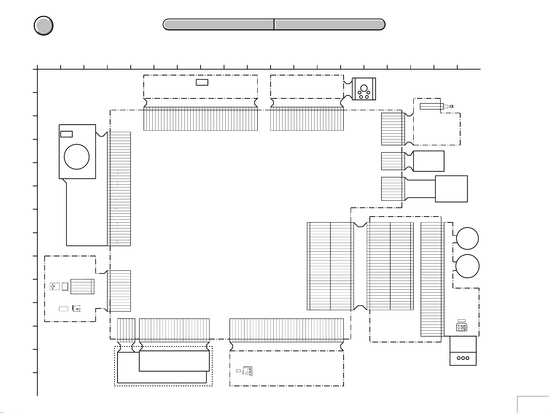
PRINTED WIRING BOARDS AND SCHEMATIC DIAGRAMS
4-1. FRAME SCHEMATIC DIAGRAM
SECTION 4
4-2. SCHEMATIC DIAGRAMS 4-3. PRINTED WIRING BOARDS
4-2. SCHEMATIC DIAGRAMS 4-3. PRINTED WIRING BOARDS
DSC-V1
1
FRAME SCHEMATIC DIAGRAM
A
B
C
LENS UNIT
OVF
D
LENS
E
F
G
H
JK-254
I
J
FLEXIBLE
BOARD
(USB)
A/V OUT
(MONO)
CN201
5P
GND
ID
D+
D-
VCC
J201
K
L
CCD
21V8
R
813184
14CCD_OUT
15GND
16GND
17GND
18VSUB_CONT
19VSUB
20GND
TEST2
RGT
B
23
24
10GND
11
12GND
13GND
CAM_15V
SY-089
BOARD
39P
CN751
STB_FULL
123456789
9
1GND
2H1A
3H2A
4GND
5RG
6GND
7H1B
8H2B
9GND
N.C.
N.C.
XSTRB_PWRSAVE
ST_UNREG
STRB_ON
ST_UNREG
ST_UNREG
M_5V
25
NC
25P
KEY_AD2
C704
ST_UNREG
ST_UNREG
N.C.
N.C.
ST_UNREG
1011121314151617181920212223242526272829303132
REG_GND
Program_Dial_B
Program_Dial_A
REG_GND
REG_GND
REG_GND
EVER_3.0V
XCHARGE_LED
REG_GND
REG_GND
127 15
CONTROL
SWITCH
BLOCK
(MODE-51470)
HOT
REG_GND
N.C.
LANC_DC
343536
REG_GND
LANC_SIG
STRB_PLUNGER
N.C.
373839
123456789
XSHTR_ON
XAE_LOCK_ON
VL_3V
BATT_UNREG
ACV_UNREG
USB_3.2V
USB_3.2V
CAM_3.2V
CAM_3.2V
A_2.9V
A_2.9V
D_2.9V
D_2.9V
D_2.9V
D_1.5V
D_1.5V
D_1.5V
CAM_P_5V
CAM_P_5V
CAM_P_5V
CAM_P_5V
CAM_15V
CAM_15V
PANEL_13.5V
CAM_-7.5V
PANEL_2.9V
EVER_3.0V
LANC_5.5V
ST_UNREG
ST_UNREG
ST_UNREG
STRB_PLUNGER
STRB_PLUNGER
XTALLY_LED
AE_LOCK_LED
REG_GND
REG_GND
D_2.9V
REG_GND
XPWR_ON
PWR_LED_ON
LD_OUT
REG_GND
MODE_DIAL
XSETUP_ON
60
58
56
54
52
50
48
46
44
42
40
38
36
34
32
30
28
26
24
22
20
18
16
14
12
10
8
6
4
2
REG_GND
PD_OUT
REG_GND
MODE_DIAL2
60PCN701
SP-
SP+
REG_GND
XRESET_FR
FAST_CHARGE
INIT_CHARAGE
BATT_SIG
BATT/XEXT
BL_THH
BL_THL
BL_H
BL_L
BL_LEVEL
BL_ON
REG_GND
REG_GND
REG_GND
REG_GND
REG_GND
REG_GND
REG_GND
REG_GND
REG_GND
REG_GND
REG_GND
REG_GND
DATA
XCS
CLK
SYS_DD_ON
XSTRB_POPUP
LANC_GND
101112131415161718192021222324
XPB_ON
LANC_SIG
KEY_AD3
LANC_GND
LANC_JACK_IN2
EXT1_STB_ON
INTE_STRB_ON
ACC_XLANC_JACK_IN
33
REG_GND
MIC_SIG
MIC_GND
XSELF_TIMER_LED
PANEL_2.9V
IR_LED_K
IR_LED_K
IR_LED_A
IR_LED_A
KEY_AD4
REG_GND
CN703
KEY_AD2
KEY_AD1
KEY_AD0
REG_GND
REG_GND
DD-195
BOARD
16
11PCN753
6P
NC
8PCN705
VSS
VCC
SCLK
INT
DIO
NC
BS
VSS
FAST_CHARGE
INIT_CHARAGE
SYS_DD_ON
11
10
9
8
7
6
5
4
3
2
1
6
5
4
3
2
1
8
7
6
5
4
3
2
1
REG_GND
XRESET_FR
BATT_SIG
BATT/XEXT
BL_THH
BL_THL
BL_LEVEL
REG_GND
REG_GND
REG_GND
REG_GND
REG_GND
REG_GND
REG_GND
REG_GND
REG_GND
REG_GND
REG_GND
REG_GND
BL_H
BL_ON
DATA
1410 19
INTELLIGENT
SHOE
60PCN082
59
57
55
53
51
49
47
45
43
41
39
37
35
33
31
29
27
25
23
21
19
17
15
13
11
9
7
5
3
1
59
VL_3V
57
BATT_UNREG
55
ACV_UNREG
53
USB_3.2V
51
USB_3.2V
49
CAM_3.2V
47
CAM_3.2V
45
A_2.9V
43
A_2.9V
41
D_2.9V
39
D_2.9V
37
D_2.9V
35
D_1.5V
33
D_1.5V
31
D_1.5V
29
CAM_P_5VCAM_P_5V
27
CAM_P_5V
25
CAM_P_5V
23
CAM_P_5V
21
CAM_P_5V
19
CAM_15V
17
CAM_15V
15
PANEL_13.5V
BB-004 FLEXIBLE BOARD
13
CAM_-7.5V
11
PANEL_2.9V
9
EVER_3.0V
7
LANC_5.5V
5
CN402 60P
3
1
ST_UNREG
ST_UNREG
ST_UNREG
CN401 60P
SP+
BL_L
XCS
CLK
SP-
MS-165
FLEXIBLE
BOARD
60
58
56
54
52
50
48
46
44
42
40
38
36
34
32
30
28
26
24
22
20
18
16
14
12
10
8
6
4
2
17
MIC_GND
MIC_SIG
SW-395
FLEXIBLE
BOARD
CONTROL
SWITCH
BLOCK
(GL-51470)
BATT_GND1
BATT_GND1
BATT_GND1
BATT_GND1
BATT_GND1
BATT_GND1
BATT_GND1
BATT_GND1
BATT_UNREG1
BATT_UNREG1
BATT_UNREG1
BATT_UNREG1
BATT_UNREG1
BATT_UNREG1
BATT_UNREG1
BATT_UNREG1
BATT_GND1
BATT_GND1
BATT/XEXT1
ACV_UNREG1
ACV_UNREG1
ACV_UNREG1
ACV_UNREG1
ACV_UNREG1
ACV_UNREG1
ACV_UNREG1
ACV_UNREG1
BATT_SIG1
ACV_GND1
ACV_GND1
ACV_GND1
ACV_GND1
ACV_GND1
ACV_GND1
ACV_GND1
ACV_GND1
2PCN101
39PCN081
VL_3V
SP+
SP-
MIC901
MICROPHONE
1
2
MS
CONNECTOR
39
38
37
36
35
34
33
32
31
30
29
28
27
26
25
24
23
22
21
20
19
18
17
16
15
14
13
12
11
FLEXIBLE
10
9
8
7
6
5
4
3
2
1
BATTERY
TERMINAL
SP901
SPEAKER
BT101
LITHIUM
BATTERY
FU-165
BOARD
J101
DC IN
BT901
32
39PCN301
1
IR_FILTTER+
2
IR_FILTTER+
3
IR_FILTTER-
4
IR_FILTTER-
5
IR_SENS_VCC
6
IR_SENS_RST
7
IR_SENS_GND
8
F_RST_SENS
9
F_RST_VCC
10
TEMP_OUT
11
TEMP_GND
12
FOCUS_B
FOCUS_B
13
FOCUS_B
14
FOCUS_B
15
16
FOCUS_A
17
FOCUS_A
FOCUS_A
18
19
FOCUS_A
SHUTTER-
20
SHUTTER-
21
22
SHUTTER+
23
SHUTTER+
24
IRIS-B
25
IRIS-B
26
IRIS-A
27
IRIS-A
28
Z_RST_SENS1
29
Z_RST_SENS2
30
Z_RST_GND
31
Z_RST_VCC
32
ZOOM_B
33
ZOOM_B
34
ZOOM_B
35
ZOOM_B
36
ZOOM_A
37
ZOOM_A
38
ZOOM_A
39
ZOOM_A
14P
CN752
USB_GND
1
USB_D+
2
USB_D-
3
USB_GND
5
4
3
2
1
4
USB_JACK_IN
5
STATIC_GND
6
STATIC_GND
7
GND_GUARD(REG_GND)
8
A_OUT
9
GND_GUARD(REG_GND)
10
AV_JACK_IN
11
GND_GUARD(REG_GND)
12
V_OUT
13
REG_GND
14
6P
N.C
BL_THL
CN702
12345
BL_THH
56 11
CD-441
FLEXIBLE BOARD
22V7B
23V7A
24V6
25Vhold
26V5B
27V5A
28V4
29Vst
30V3B
31V3A
32V2
33V1B
34
35GND
36CCD_TEMP
373839GND
BL_L
BL_H
N.C
6
39P
CN151
24P
COM
TEST1
CN801
1234567
VST
CAM_-7.5V
VCK
V1A
GND
DWN
VSSG
EN
VDDG
VSS
VDD
8
9
10111213141516171819202122
REF
HST
WIDE
G
CRext
PSIG
HCK1
HCK2CSSOUT
M
LCD901
COLOR LCD MONITOR
J301
ACC
ST-083
FLEXIBLE BOARD
D901 BACKLIGHT
N
05
PANEL UNIT
4-1 4-2
FRAME
Page 10
COVER
COVER
Link
Link
DSC-V1
4-2. SCHEMATIC DIAGRAMS
BB-004 FLEXIBLE BOARD
CD-441 FLEXIBLE BOARD
CD-441 FLEXIBLE BOARD
ST-083 FLEXIBLE BOARD
ST-083 FLEXIBLE BOARD
(FLASH DRIVE, LASER UNIT)
(FLASH DRIVE, LASER UNIT)
SW-395 FLEXIBLE BOARD
SW-395 FLEXIBLE BOARD
(MIC, LENS ADAPTOR SWITCH)
(MIC, LENS ADAPTOR SWITCH)
JK-254 FLEXIBLE BOARD (USB, A/V JACK) CONTROL SWITCH BLOCK (MODE-51470)
JK-254 FLEXIBLE BOARD (USB, A/V JACK) CONTROL SWITCH BLOCK (MODE-51470)
MS-165 FLEXIBLE BOARD
MS-165 FLEXIBLE BOARD
(MEMORY STICK CONNECTOR)
(MEMORY STICK CONNECTOR)
COMMON NOTE FOR SCHEMATIC DIAGRAMS
COMMON NOTE FOR SCHEMATIC DIAGRAMS
(CCD IMAGER)
(CCD IMAGER)
BB-004 FLEXIBLE BOARD
(SY-DD EXTENSION BOARD)
(SY-DD EXTENSION BOARD)
FU-165 FLEXIBLE BOARD
FU-165 FLEXIBLE BOARD
(DC IN, BATTERY IN)
(DC IN, BATTERY IN)
CONTROL SWITCH BLOCK (GL-51470)
CONTROL SWITCH BLOCK (GL-51470)
Page 11
COVER
COVER
For Schematic Diagram
• Refer to page 4-49 for printed wiring board.
4-2. SCHEMATIC DIAGRAMS CD-441 FLEXIBLE BOARD
4-2. SCHEMATIC DIAGRAMS CD-441 FLEXIBLE BOARD
DSC-V1
1
CD-441 FLEXIBLE BOARD
A
CCD IMAGER(CCD BLOCK)
3
482
5
Note:Voltage and waveform of mounted on CD-441 flexible
board can not be measured because they are mounted
by the side of the lens.
6
7
XX MARK:NO MOUNT
LND101
39
LND102
B
C
D
SY-089
(1/12)
CN151
(PAGE 4-9)
E
F
LND103
LND104
LND105
LND106
LND107
LND108
LND109
LND110
LND111
LND112
LND113
LND114
LND115
LND116
LND117
LND118
LND119
LND120
LND121
LND122
LND123
LND124
LND125
LND126
LND127
LND128
LND129
LND130
LND131
LND132
LND133
LND134
LND135
LND136
LND137
LND138
LND139
38
37
36
35
34
33
32
31
30
29
28
27
26
25
24
23
22
21
20
19
18
17
16
15
14
13
12
11
10
9
8
7
6
5
4
3
2
1
SIGNAL PATH
G
VIDEO
SIGNAL
Y/CHROMA
REC
CAM_-7.5V
CCD_TEMP
Vhold
VSUB
VSUB_CONT
CCD_OUT
CAM_15V
GND
GND
GND
GND
GND
GND
GND
GND
GND
GND
GND
GND
GND
GND
V1A
V1B
V3A
V3B
V5A
V5B
V7A
V7B
H2B
H1B
H2A
H1A
TH101
V2
Vst
V4
V6
V8
R104
3300
R103
470k
C105
R106
6
Vhld
7V48
V5A9V5B
10
14
0
11v612
V8
V7A13V7B
3v24
1
Vst
V1A2V1B
V3A5V3B
IC101
CCD IMAGER
IC101
ICX455AQF-13
XX
C106
XX
16V
VOUT16GND17GND18GND19VDD20RG21H2B22H1B23SUB24CSUB25NC26VL27H1A28H2A
15
R110
680
R111
C108
0
0.1u
C107
0.22u
16V
16V
C109
10u
16V
C110
0.1u
16V
Precautions for Replacement of CCD Imager
•The CD-441 flexible board mounted as a repair part is not
C103
XX
R101
1500
Q102
BUFFER
FB101
1/10W
C101
0.1u
16V
Q101
UN9213J-(K8).SO
SWITCH
RG
2SC4250(T5LSONY1)
equipped with a CCD imager.
When replacing this board, remove the CCD imager from the
old one and mount it onto the new one.
• If the CCD imager has been replaced, carry out all the
adjustments for the camera section.
H
• As the CCD imager may be damaged by static electricity from
its structure, handle it carefully like for the MOS IC.
In addition, ensure that the receiver is not covered with dusts
05
nor exposed to strong light.
4-7 4-8
CD-441
Page 12

Schematic diagrams of the SY-089 and DD-195 boards are not shown.
Pages from 4-9 to 4-36 are not shown.
Page 13
DSC-V1
COVER
COVER
For Schematic Diagram
• Refer to page 4-57 for printed wiring board.
4-2. SCHEMATIC DIAGRAMS ST-083 FLEXIBLE BOARD
4-2. SCHEMATIC DIAGRAMS ST-083 FLEXIBLE BOARD
1
3
482 10
5
6
7
9
ST-083 FLEXIBLE BOARD
A
B
C
D
E
F
G
FLASH DRIVE,LASER UNIT(STROB BLOCK)
XX MARK:NO MOUNT
NO MARK:REC/PB MODE
STRB_PLUNGER
39
SY-089
(11/12)
CN751
(PAGE 4-29)
LND389
LND388
LND387
LND386
LND385
LND384
LND383
LND382
LND381
LND380
LND379
LND378
LND377
LND376
LND375
LND374
LND373
LND372
LND371
LND370
LND369
LND368
LND367
LND366
LND365
LND364
LND363
LND362
LND361
LND360
LND359
LND358
LND357
LND356
LND355
LND354
LND353
LND352
LND351
38
37
36
35
34
33
32
31
30
29
28
27
26
25
24
23
22
21
20
19
18
17
16
15
14
13
12
11
10
9
8
7
6
5
4
3
2
1
STRB_PLUNGER
STRB_PLUNGER
N.C.
N.C.
LANC_DC
ACC_XLANC
_JACK_IN
EXT1_STB_ON
LANC_GND
LANC_SIG
LANC_GND
XSTRB_POPUP
PD_OUT
REG_GND
LD_OUT
REG_GND
REG_GND
REG_GND
REG_GND
REG_GND
REG_GND
REG_GND
REG_GND
REG_GND
REG_GND
N.C.
N.C.
ST_UNREG
ST_UNREG
ST_UNREG
ST_UNREG
ST_UNREG
ST_UNREG
N.C.
XSTRB_PWRSAVE
STRB_ON
M_5V
N.C.
STB_FULL
C338
10u
6.3V
CPH3209-SONY-TL-E
LND305
STRB_PLUNGER
LND304
REG_GND
STROBE OPEN
Q331
Q331,Q332
TRANS DRIVE
S301
DETECT
0
MA111-(K8).S0
D331
PLUNGER
R331
5600
0
R333
100k
0
R334
10k
R332
1800
0
FB302
FB305
R302
5.6
0
Q332
MCH3405-TL-E
T331
R335
560
4
1
5
6
2
3
7
1
P
2
C331
0.22u
IC331
FLASH CONTROL
IC331
TND721MH5-S-TL-E
3.GND
S
F
J301
ACC
LND390
+
SIDE
FOR DISCHARGING
L331
R337
C334
0.047u
250V
1M
LND331
XE_H
Cathode
XE_L
LND332
Q334
FLASH DRIVE
5
7
8
Anode
LND391
GND
1
2
34
LND333
TRIGGER
268
1.LD2.PD
D333
LASER
UNIT
(Note)
HAU160C030TP
4
IN
5
GND
VDD
OUT
2
1
NC
D332
315V
CHARGING
CAPACITOR
3
2
1
3
C333
135u
C337
FLASH
UNIT
CY25BAJ-8F-T23
6
R338
47
0
R339
XX
1M
5
4
3
ST-083
05
(Note) Be sure to read “SERVICE NOTE” on page 1-2
when replacing the laser unit (D333).
The components identified by mark 0 or dotted
line with mark 0 are critical for safety.
Replace only with part number specified.
Les composants identifiés par une marque 0 sont
critiques pour la sécurité. Ne les remplacer que
par une piéce portant le numéro spécifié.
4-37 4-38
Page 14
COVER
COVER
4-2. SCHEMATIC DIAGRAMS
4-2. SCHEMATIC DIAGRAMS
SW-395 FLEXIBLE BOARD
SW-395 FLEXIBLE BOARD
JK-254, MS-165
JK-254, MS-165
FLEXIBLE BOARD
FLEXIBLE BOARD
DSC-V1
For Schematic Diagram
• Refer to page 4-59 for printed wiring board.
1
SW-395 FLEXIBLE BOARD
A
MIC,LENS ADAPTOR SWITCH(SW BLOCK)
LND101
1
2
3
4
5
6
7
8
9
10
11
AUDIO
SIGNAL
REG_GND
KEY_AD4
IR_LED_A
IR_LED_A
IR_LED_K
IR_LED_K
PANEL_2.9V
XSELF_TIMER
MIC_GND
MIC_SIG
REG_GND
_LED
LND102
B
SY-089
(11/12)
CN753
(PAGE 4-30)
LND103
LND104
LND105
LND106
LND107
LND108
LND109
LND110
LND111
C
SIGNAL PATH
D
REC
342
S101
LENS ADAPTOR
DETECT
D102
CL-196HR-CD-T
(SELF TIMER)(RED)
For Schematic Diagram
• Refer to page 4-61 for printed wiring board.
5
6
1
342
5
6
MS-165 FLEXIBLE BOARD
A
MEMORY STICK CONNECTOR
VSS
VCC
SCLK
N.C.
INT
N.C.
DIO
N.C.
BS
VSS
LND020
LND019
LND018
LND017
LND016
LND015
LND014
LND013
LND012
LND011
MEMORY
STICK
MS
CONNECTOR
MEMORY STICK
D101
2
1
DCZ2805
(IR EMITTER)
(IR)
3
R101
1
2
2PCN101
REG_GND
MIC_SIG
REG_GND
470
LND112
MIC901
MICROPHONE
B
SY-089
(6/12)
CN705
(PAGE 4-19)
C
LND008
LND007
LND006
LND005
LND004
LND003
LND002
LND001
7
VCC
SCLK
6
5
INT
DIO
4
3
N.C.
2
BS
1
VSS
VSS
8
10
9
8
7
6
5
4
3
2
1
SIGNAL PATH
VIDEO SIGNAL
Y/CHROMA
AUDIO
SIGNAL
REC
D
PB
05
For Schematic Diagram
• Refer to page 4-61 for printed wiring board.
1
JK-254 FLEXIBLE BOARD
A
USB,A/V JACK(JK BLOCK)
CN201 5P
GND
ID
B
(USB)
C
A/V OUT
(MONO)
J201
D+
D-
VCC
05
1
2
3
4
5
6
7
GND_GUARD(REG_GND)
8
9
GND_GUARD(REG_GND)
10
11
GND_GUARD(REG_GND)
12
13
14
5
USB_GND
USB_D+
USB_D-
USB_GND
USB_JACK_IN
STATIC_GND
STATIC_GND
A_OUT
AV_JACK_IN
V_OUT
REG_GND
LND201
LND202
LND203
LND204
LND205
LND206
LND207
LND208
LND209
LND210
LND211
LND212
LND213
LND214
6
SY-089
(9/12)
CN752
(PAGE 4-26)
342
5
4
3
2
1
LND215
STATIC_GND
SIGNAL PATH
D
VIDEO SIGNAL
Y/CHROMA
AUDIO
SIGNAL
REC
PB
E
05
4-39
4-40
SW-395, JK-254, MS-165
Page 15
DSC-V1
COVER
COVER
4-2. SCHEMATIC DIAGRAMS BB-004 FLEXIBLE BOARD
4-2. SCHEMATIC DIAGRAMS BB-004 FLEXIBLE BOARD
For Schematic Diagram
• Refer to page 4-62 for printed wiring board.
1
32
56
7
84
9
BB-004 FLEXIBLE BOARD
A
SY-DD EXTENSION BOARD
B
C
D
E
F
2
4
6
8
10
12
14
16
18
20
22
24
26
28
30
32
34
36
38
40
42
44
46
48
50
52
54
56
58
60
SYS_DD_ON
CLK
XCS
DATA
REG_GND
REG_GND
REG_GND
REG_GND
REG_GND
REG_GND
REG_GND
REG_GND
REG_GND
REG_GND
REG_GND
REG_GND
BL_ON
BL_LEVEL
BL_L
BL_H
BL_THL
BL_THH
BATT/XEXT
BATT_SIG
INIT_CHARAGE
FAST_CHARGE
XRESET_FR
REG_GND
SP+
SP-
SY-089
(12/12)
CN701
(PAGE 4-31) (PAGE 4-33)
60PCN401
ST_UNREG
ST_UNREG
ST_UNREG
LANC_5.5V
EVER_3.0V
PANEL_2.9V
CAM_-7.5V
PANEL_13.5V
CAM_15V
CAM_15V
CAM_P_5V
CAM_P_5V
CAM_P_5V
CAM_P_5V
CAM_P_5V
D_1.5V
D_1.5V
D_1.5V
D_2.9V
D_2.9V
D_2.9V
A_2.9V
A_2.9V
CAM_3.2V
CAM_3.2V
USB_3.2V
USB_3.2V
ACV_UNREG
BATT_UNREG
VL_3V
1
3
5
7
9
11
13
15
17
19
21
23
25
27
29
31
33
35
37
39
41
43
45
47
49
51
53
55
57
59
1
3
5
7
9
11
13
15
17
19
21
23
25
27
29
31
33
35
37
39
41
43
45
47
49
51
53
55
57
59
ST_UNREG
ST_UNREG
ST_UNREG
LANC_5.5V
EVER_3.0V
PANEL_2.9V
CAM_-7.5V
PANEL_13.5V
CAM_15V
CAM_15V
CAM_P_5V
CAM_P_5V
CAM_P_5V
CAM_P_5V
CAM_P_5V
D_1.5V
D_1.5V
D_1.5V
D_2.9V
D_2.9V
D_2.9V
A_2.9V
A_2.9V
CAM_3.2V
CAM_3.2V
USB_3.2V
USB_3.2V
ACV_UNREG
BATT_UNREG
VL_3V
DD-195
(1/2)
CN082
60PCN402
SYS_DD_ON
BATT/XEXT
INIT_CHARAGE
FAST_CHARGE
XRESET_FR
DATA
REG_GND
REG_GND
REG_GND
REG_GND
REG_GND
REG_GND
REG_GND
REG_GND
REG_GND
REG_GND
REG_GND
REG_GND
BL_ON
BL_LEVEL
BL_H
BL_THL
BL_THH
BATT_SIG
REG_GND
BL_L
2
CLK
4
XCS
6
8
10
12
14
16
18
20
22
24
26
28
30
32
34
36
38
40
42
44
46
48
50
52
54
56
SP+
58
SP-
60
BB-004
4-41
G
H
SIGNAL PATH
AUDIO
SIGNAL
I
05
PB
4-42
Page 16
COVER
COVER
For Schematic Diagram
• Refer to page 4-63 for printed wiring board.
4-2. SCHEMATIC DIAGRAMS FU-165 FLEXIBLE BOARD
4-2. SCHEMATIC DIAGRAMS FU-165 FLEXIBLE BOARD
DSC-V1
1
3
42
5
6
FU-165 FLEXIBLE BOARD
A
B
DC IN,BATTERY IN(FUSE BLOCK)
J101
DC IN
5P
LND110
LND107
LND109
LND108
LND111
STATIC_GND
ACV_UNREG1
BATT/XEXT1
ACV_GND1
STATIC_GND
LND101
STATIC_GND
C
LND106
SP901
SPEAKER
LND105
SP-
SP+
BT101
LITHIUM
BATTERY
LND112
LND113
VL_3V
ACV_GND1
D
LND102
BT901
BATTERY
TERMINAL
S
E
F
LND103
LND104
BATT_UNREG
BATT_SIG
BATT_GND
SIGNAL PATH
AUDIO
SIGNAL
PB
ACV_UNREG1
1
ACV_UNREG1
2
3
ACV_UNREG1
ACV_UNREG1
4
5
ACV_UNREG1
6
ACV_UNREG1
ACV_UNREG1
7
8
ACV_UNREG1
BATT/XEXT1
9
10
ACV_GND1
ACV_GND1
11
ACV_GND112
13
ACV_GND1
ACV_GND1
14
15
ACV_GND1
ACV_GND1
16
17
ACV_GND1
BATT_GND1
18
SP-
19
SP+
20
BATT_GND1
21
22
VL_3V
BATT_UNREG1
23
24
BATT_UNREG1
25
BATT_UNREG1
26
BATT_UNREG1
27
BATT_UNREG1
28
BATT_UNREG1
BATT_UNREG1
29
30
BATT_UNREG1
31
BATT_SIG1
32
BATT_GND1
33
BATT_GND1
BATT_GND1
34
BATT_GND1
35
36
BATT_GND1
BATT_GND1
37
BATT_GND1
38
39
BATT_GND1
LND151
LND152
LND153
LND154
LND155
LND156
LND157
LND158
LND159
LND160
LND161
LND162
LND163
LND164
LND165
LND166
LND167
LND168
LND169
LND170
LND171
LND172
LND173
LND174
LND175
LND176
LND177
LND178
LND179
LND180
LND181
LND182
LND183
LND184
LND185
LND186
LND187
LND188
LND189
DD-195
(1/2)
CN081
(PAGE 4-33)
A
B
C
D
E
05
1
342
CONTROL SWITCH BLOCK(GL-51470)
CONTROL SWITCH BLOCK (GL-51470) is replaced as a block,
so that PRINTED WIRING BOARD is omited.
SY-089
(10/12)
CN703
(PAGE 4-27)
LND251
LND252
LND253
LND254
LND255
LND256
1
REG_GND
2
REG_GND
3
KEY_AD0
KEY_AD1
5
64KEY_AD2
(RIGHT)/MACRO
IMAGE SIZE/DELETE
(DOWN)/SELF TIMER
MENU (UP)/FLASH
NC
S254
R251
3300
S253
R252
1500
S252
R253
1200
S251 S255
R257
1200
S259
R258
1500
DISPLAY/
LCD ON/OFF
(LEFT)/REVIEW
S260
5
(SET)
R254
3300
R255
1500
R256
1200
R259
3300
6
S258
S257
S256
S261
AE LOCKFOCUSEXPOSURE/INDEX
05
The components identified by mark 0 or dotted
line with mark 0 are critical for safety.
Replace only with part number specified.
Les composants identifiés par une marque 0 sont
critiques pour la sécurité. Ne les remplacer que
par une piéce portant le numéro spécifié.
4-43
4-44
FU-165, GL-51470
Page 17
DSC-V1
COVER
COVER
4-2. SCHEMATIC DIAGRAMS
4-2. SCHEMATIC DIAGRAMS
1
428109
5 12
6
7
113
CONTROL SWITCH BLOCK (MODE-51470)
A
CONTROL SWITCH BLOCK (MODE-51470) is replaced as a block,
so that PRINTED WIRING BOARD is omited.
B
MAZT082H08S0
MAZT082H08S0
D101
D113
1SS387-TPL3
D102
C
D
CN100
25P
XAE_LOCK_ON
E
INTE_STRB_ON
LANC_JACK_IN2
F
SY-089
(10/12)
CN704
(PAGE 4-27)
G
MODE_DIAL2
MODE_DIAL
XSETUP_ON
PWR_LED_ON
XTALLY_LED
AE_LOCK_LED
XCHARGE_LED
Program_Dial_B
Program_Dial_A
XSHTR_ON
REG_GND
LANC_SIG
REG_GND
KEY_AD3
XPB_ON
REG_GND
XPWR_ON
D_2.9V
EVER_3.0V
KEY_AD2
1
2
3
4
5
HOT
6
7
8
9
10
11
12
13
14
15
16
17
18
19
20
21
22
23
24
NC
25
H
MAZT082H08S0
D103
STATIC_GND
LND100
MAZT082H08S0
D104
MAZT082H08S0
D109
MAZT082H08S0
D110
C100
0.01u
R112
R113
03P4J
1k
D112
R114
S103
(SHUTTER)
(DOWN)
SCENE
XPWR_ON
(2nd)
1
2
(1st)
3
4
ZOOM
R107
S105S101
1200
(UP)
(OFF) NIGHTSHOT
S102
R108
4700
0.5%
R109
6800
S108
(MODE DIAL)
5
A
6
B
C
POWER
S104
4
3
10
2
1
R110
3300
MANUAL
AE-A
AE-S
P_AUTO
1500
1200
R115
R116
XSHTR_ON
XAE_LOCK_ON
0
0
LANC_SIG
REG_GND
HOT
INTE_STRB_ON
LANC_JACK_IN2
SHOE_GND
LND101
LND102
LND103
LND104
LND105
LND106
INTELLIGENT
SHOE
D105
TLGV1021(T15SOY2,F)
(POWER)(GREEN)
D106
TLRMV1021(T15SOY,F)
(SELF TIMER/RECORDING)(RED)
D107
TLGV1021(T15SOY2,F)
(AE/AF LOCK)(GREEN)
D108
TLYV1021(T15SOY,F)
/CHG
(ORANGE)
R105
6800
1200
R104
NIGHTFRAMING
SET_UP
MOVIE
PLAY
AUTO
R103
270
R100
1200
R101
470
R102
820
MODE-51470
I
J
05
The components identified by mark 0 or dotted
line with mark 0 are critical for safety.
Replace only with part number specified.
4-45 4-46
DIAL_A
S106
(JOG DIAL)
EXECUTE
DIAL_B
Les composants identifiés par une marque 0 sont
critiques pour la sécurité. Ne les remplacer que
par une piéce portant le numéro spécifié.
Page 18
COVER
COVER
Link
Link
DSC-V1
4-2. SCHEMATIC DIAGRAMS
SY-089 BOARD (1/12)
SY-089 BOARD (1/12)
SY-089 BOARD (2/12)
SY-089 BOARD (2/12)
SY-089 BOARD (3/12)
SY-089 BOARD (3/12)
SY-089 BOARD (4/12)
SY-089 BOARD (4/12)
SY-089 BOARD (5/12)
SY-089 BOARD (5/12)
SY-089 BOARD (6/12)
SY-089 BOARD (6/12)
(MEMORY, CLOCK GENERATOR)
(MEMORY, CLOCK GENERATOR)
SY-089 BOARD (7/12)
SY-089 BOARD (7/12)
(LCD DRIVE, TIMING GENERATOR)
(LCD DRIVE, TIMING GENERATOR)
(CAMERA MODULE)
(CAMERA MODULE)
(SIGNAL GENERATOR)
(SIGNAL GENERATOR)
(LENS DRIVE)
(LENS DRIVE)
(CAMERA DSP)
(CAMERA DSP)
(SH DSP)
(SH DSP)
SY-089 BOARD (8/12)
SY-089 BOARD (8/12)
SY-089 BOARD (9/12)
SY-089 BOARD (9/12)
SY-089 BOARD (10/12)
SY-089 BOARD (10/12)
SY-089 BOARD (11/12)
SY-089 BOARD (11/12)
(AF LASER/IR LED DRIVE, FLASH CONTROL)
(AF LASER/IR LED DRIVE, FLASH CONTROL)
SY-089 BOARD (12/12)
SY-089 BOARD (12/12)
(INTELLIGENT SHOE CONTROL, DC POWER)
(INTELLIGENT SHOE CONTROL, DC POWER)
DD-195 BOARD (1/2)
DD-195 BOARD (1/2)
(DC POWER IN, CONNECTOR)
(DC POWER IN, CONNECTOR)
DD-195 BOARD (2/2)
DD-195 BOARD (2/2)
WAVEFORMSCOMMON NOTE FOR SCHEMATIC DIAGRAMS
WAVEFORMSCOMMON NOTE FOR SCHEMATIC DIAGRAMS
(AUDIO, VIDEO)
(AUDIO, VIDEO)
(USB INTERFACE)
(USB INTERFACE)
(FRONT CONTROL)
(FRONT CONTROL)
(DC/DC CONVERTER)
(DC/DC CONVERTER)
Page 19
DSC-V1
COVER
COVER
For Schematic Diagram
• Refer to page 4-51 for printed wiring board.
1
SY-089 BOARD (1/12)
A
CAMERA MODULE(CH BLOCK)
XX MARK:NO MOUNT
NO MARK:REC/PB MODE
R:REC MODE
P:PB MODE
B
C
D
CD-441
FLEXIBLE
LND101-LND139
(PAGE 4-7)
E
F
G
2
CN151
39P
1GND
2H1A
3H2A
4GND
5RG
6GND
7H1B
8H2B
9GND
10GND
11CAM_15V
12GND
13GND
14CCD_OUT
15GND
16GND
17GND
18VSUB_CONT
19VSUB
20GND
21V8
22V7B
23V7A
24V6
25Vhold
26V5B
27V5A
28V4
29Vst
30V3B
31V3A
32V2
33V1B
34V1A
35GND
36CCD_TEMP
37GND
38CAM_-7.5V
39GND
H
I
Note: Each model has its
own camera module.
J
Discrimination
method is the following.
K
4-2. SCHEMATIC DIAGRAMS
4-2. SCHEMATIC DIAGRAMS
4
C155
0.1u
C152
C151
0.22u
0.22u
R156
100k
D151
MA2S111-(K8).SO
L151
100uH
C153
3.3u
35V
5
:Voltage measurment of the CSP ICs
and the Transistors with mark,are
not possible.
1
V4
2
NC
3
C154
0.01u
V5B
4
NC
5
VH
6
NC
7
V5A
8
NC
9
V3B
NC
10
V3A
11
NC
12
VL
13
NC
14
V2
15
V1
16
50NC51
52NC53
IC151
V DRIVER
IC151
CXD3440GA-T4
54NC55NC56NC57NC58NC59NC60NC61NC62NC63VM64
XV6
VSS
V6
SUB18NC19NC20NC21NC22NC23NC24NC25NC26NC27NC28NC29MODE30NC31VDD32XSUB
17
8
49
XV4
XSG5B
48
XV5
47
NC
46
XSG5A
45
NC
44
XV3
43
NC
42
XSG3B
41
NC
40
XSG3A
39
NC
38
XV2
37
NC
36
XV1
35
NC
34
XSG1
33
0.1u
C167
SY-089 BOARD SIDE A SY-089 BOARD SIDE B
SY-089 BOARD SIDE A SY-089 BOARD SIDE B
910
CA_AD00
CA_AD01
CA_AD02
CA_AD03
CA_AD04
CA_AD05
CA_AD06
CA_AD07
CA_AD08
CA_AD09
CA_AD10
CA_AD11
CA_AD12
CA_AD13
11 15 17 183
19202122232425262728293031323334353637
38 39 40 41 42 43 44 45 46 47 48 49 50 51 52 53 54 55
XFE_CS
XTG_CS
CAM_SO
XCAM_SCK
12
IC152
CAMERA MODULE
(CH-122 (5M-V1) BOARD)
220
R161
R160 220
XCAM_RESET
CLPDM
CLPOB
IC152
220
R163
CA_HR
220
R164
CA_VR
TG_CLK
MCK12
13 1667
5.6
5.6
5.6
R167
R168
R166
(Note)
FB151
C156
0.1u
150
R165
14
Note: EMI filter is mounted to the location
where FB151 is printed.
5.6
R169
XX
C158
XX
C161
XX
C162
C163
XX
123456789101112131415161718
56 57 58 59 60 61 62 63 64 65 66 67 68 69 70 71 72 73 74
C157
47u
6.3V
TG_WEN
R170
100k
FB152
C159
47u
6.3V
C160
47U
6.3V
C164
3.3u
35V
C165
22u
16V
CA_AD00
CA_AD01
CA_AD02
CA_AD03
CA_AD04
CA_AD05
CA_AD06
CA_AD07
CA_AD08
CA_AD09
CA_AD10
CA_AD11
CA_AD12
CA_AD13
CA_VR
CA_HR
CLPOB
CLPDM
MCK12
CAM_SO
XCAM_SCK
XCAM_RESET
XTG_CS
TG_CLK
TG_WEN
XFE_CS
L152
47uH
5
R3.3
/P15
R15.1/P0
Q152
RN2907FE(TPLR3)
B+ SWITCH
15.1
C166
R3.3
0.1u
/P15
1
4
R0
/P14.9
2
3
6
R3.1
/P-7.5
R-7.6/P0
5
R0
R171
82k
/P14.8
6
3
1
4
-7.6
L153
47uH
L154
47uH
R2.9/P0
2
Q153
RN1907FE(TPLR3)
B- SWITCH
CA_ADI00
CA_ADI01
CA_ADI02
CA_ADI03
CA_ADI04
CA_ADI05
CA_ADI06
CA_ADI07
CA_ADI08
CA_ADI09
CA_ADI10
CA_ADI11
CA_ADI12
CA_ADI13
CA_FDI
CA_HDI
CLPOBI
CLPDMI
MCK12
MCK12
CAM_SO
XCAM_SCK
XCAM_RESET
XTG_CS
TG_CLK
TG_WEN
VSUB_CONT
XFE_CS
CCD_TEMP
CAM_DD_ON
CAM_3.2V
CAM_15V
CAM_-7.5V
REG_GND
1
(2/12)
2
(4/12)
3
(5/12)
4
(5/12)
5
(6/12)
6
(4/12)
7
(5/12)
8
(12/12)
L
SY-089 (1/12)
05
DSC-V1 : D3431
4-9
4-10
Page 20
DSC-V1
COVER
COVER
For Schematic Diagram
• Refer to page 4-51 for printed wiring board.
1
2
SY-089 BOARD (2/12)
A
B
C
D
E
F
G
SIGNAL GENERATOR
XX MARK:NO MOUNT
CA_AD00
CA_AD01
CA_AD02
CA_AD03
CA_AD04
CA_AD05
CA_AD06
CA_AD07
9
(4/12)
10
(5/12)
11
(5/12)
1
(1/12)
CA_AD08
CA_AD09
CA_AD10
CA_AD11
CA_AD12
CA_AD13
CA_FD
CA_HD
CLPOB
CLPDM
CAM_SO
XCAM_SCK
XCAM_RESET
XTG_CS
CA_ADI00
CA_ADI01
CA_ADI02
CA_ADI03
CA_ADI04
CA_ADI05
CA_ADI06
CA_ADI07
CA_ADI08
CA_ADI09
CA_ADI10
CA_ADI11
CA_ADI12
CA_ADI13
CA_FDI
CA_HDI
CLPOBI
CLPDMI
MCK12
CA_AD00
CA_AD01
CA_AD02
CA_AD03
CA_AD04
CA_AD05
CA_AD06
CA_AD07
CA_AD08
CA_AD09
CA_AD10
CA_AD11
CA_AD12
CA_AD13
CA_FD
CA_HD
CLPOB
CLPDM
CAM_SO
XCAM_SCK
XCAM_RESET
XTG_CS
CA_ADI00
CA_ADI01
CA_ADI02
CA_ADI03
CA_ADI04
CA_ADI05
CA_ADI06
CA_ADI07
CA_ADI08
CA_ADI09
CA_ADI10
CA_ADI11
CA_ADI12
CA_ADI13
CA_FDI
CA_HDI
CLPOBI
CLPDMI
MCK12
CA_FDI
CLPDMI
CA_HDI
CLPOBI
CA_ADI00
CA_ADI02
MCK12
CA_ADI01
CA_ADI03
CA_ADI05
C681
4-2. SCHEMATIC DIAGRAMS
4-2. SCHEMATIC DIAGRAMS
5
SY-089 BOARD SIDE A SY-089 BOARD SIDE B
SY-089 BOARD SIDE A SY-089 BOARD SIDE B
67
9843
10
:Voltage measurment of the CSP ICs
and the Transistors with mark,are
not possible.
CA_AD11
CA_AD12
CA_AD13
XX
C683
1u
45
46
47
48
ADOUT13
ADOUT12
CCDFDOUT
CLPDUMOUT
49
CCDHDOUT
50
VDDE
51
CLPOPBOUT
52
VSS
53
XTST
54
VDDI
55
ADIN00
56
ADIN02
57
CLK
58
VSS
59
VDDE
60
ADIN01
61
ADIN04
62
ADIN03
63
ADIN05
64
ADIN072ADIN063ADIN094ADIN085VDDE6ADIN107VSS8ADIN119ADIN1310ADIN1211XSM12VDDI13SCK14VPD15SMCK16CLPDUMIN
1
CA_AD09
CA_AD10
41
42
43
44
VSS
VDDE
ADOUT11
ADOUT09
IC681
SIGNAL GENERATOR,SRAM
IC681
CXD3176GA-T2
CA_AD08
40
ADOUT08
ADOUT10
39
CA_AD06
38
VDDI
CA_AD07
37
ADOUT06
CA_AD05
36
ADOUT05
ADOUT07
35
34
VDDE
CA_AD04
33
ADOUT04
VSS
ADOUT03
ADOUT02
ADOUT01
ADOUT00
VDDE
TEST0
XRST
CCDHDIN
SDATA
CCDFDIN
CLPOPBIN
VSS
MST
VSS
VDDI
XCS
C684
0.1u
REG_GND
12
D_1.5V
D_2.9V
C687
22u
32
31
30
29
28
27
26
25
24
23
22
21
20
19
18
17
C686
0.1u
CA_AD03
CA_AD02
CA_AD01
CA_AD00
XCAM_RESET
CA_HD
CAM_SO
CA_FDCA_ADI04
CLPOB
XTG_CS
(12/12)
SIGNAL PATH
C682
XX
CLPDM
XCAM_SCK
VIDEO
SIGNAL
Y/CHROMA
REC
CA_ADI07
CA_ADI06
CA_ADI09
CA_ADI08
CA_ADI10
CA_ADI11
CA_ADI13
CA_ADI12
H
05
4-11
4-12
SY-089 (2/12)
Page 21
DSC-V1
COVER
COVER
4-2. SCHEMATIC DIAGRAMS
4-2. SCHEMATIC DIAGRAMS
For Schematic Diagram
• Refer to page 4-51 for printed wiring board.
1
SY-089 BOARD (3/12)
A
LENS DRIVE(LD BLOCK)
XX MARK:NO MOUNT
NO MARK:REC/PB MODE
R:REC MODE
P:PB MODE
B
C
D
LENS
UNIT
E
F
LENS UNIT is replaced as a block.
So that there PRINTED WIRING BOARD and
SCHEMATIC DIAGRAM are omitted.
G
CN301
IR_FILTTER+
IR_FILTTER+
IR_FILTTER-
IR_FILTTER-
IR_SENS_VCC
IR_SENS_RST
IR_SENS_GND
F_RST_SENS
F_RST_VCC
TEMP_OUT
TEMP_GND
FOCUS_B
FOCUS_B
FOCUS_B
FOCUS_B
FOCUS_A
FOCUS_A
FOCUS_A
FOCUS_A
SHUTTER-
SHUTTER-
SHUTTER+
SHUTTER+
Z_RST_SENS1
Z_RST_SENS2
Z_RST_GND
Z_RST_VCC
ZOOM_B
ZOOM_B
ZOOM_B
ZOOM_B
ZOOM_A
ZOOM_A
ZOOM_A
ZOOM_A
IRIS-B
IRIS-B
IRIS-A
IRIS-A
2
39P
1
2
3
4
5
6
7
8
9
10
11
12
13
14
15
16
17
18
19
20
21
22
23
24
25
26
27
28
29
30
31
32
33
34
35
36
37
38
39
H
I
J
FOCUS_B
FOCUS_B
FOCUS_A
FOCUS_A
SHUTTER-
SHUTTER+
ZOOM_B
ZOOM_B
ZOOM_A
ZOOM_A
IRIS_B
IRIS_B
IRIS_A
IRIS_A
SY-089 BOARD SIDE A SY-089 BOARD SIDE B
SY-089 BOARD SIDE A SY-089 BOARD SIDE B
4 11893
C302
0.1u
L302
10uH
10uH
L303
5 12
:Voltage measurment of the CSP ICs
and the Transistors with mark,are
not possible.
C304
0.1u
R0/P5
CP1
25
R0/P5
CP2
26
CP3
27
CP4
28
R9.9/P4.6
C305
0.1u
R2.8/P0
VG
29
DGND
30
0.6
VLIM
31
VREF
32
PS
33
2.9
VCC
34
BR6
35
BR5
36
C317
22u
C306
10V
XX
FOCUS_B
FOCUS_B
R0.8/P0
R0.8/P05R0.9/P0
22
23
VM2
OUT4A24OUT4B
OUT5A38OUT5B39VM340PGND2
37
5
R1.1/P0.6
R1.1/P0.6
ZOOM_A
ZOOM_A
6
IRIS_B
IRIS_B
FOCUS_A
FOCUS_A
R1.5/P0
R2.1/P0
R2.9/P05R2.9/P0
16
17
19
20
21
OUT2A18OUT2B
OUT3A
OUT3B
PGND1
IC303
LENS DRIVER
IC303
BD6752AKV-E2
OUT6A42OUT6B43OUT7A44RNF45VM446OUT7B47EN748IN7
41
0
5
R1/P0.5
R1/P0.5
R1/P0.5
22u 10V
C316
R308
XX
2.2
5%
C310
ZOOM_B
ZOOM_B
SHUTTER+
IRIS_A
VM1
R0.1/P0.7
SHUTTER-
7
IRIS_A
R2.1/P0
0
13
14
CNF
OUT1A15OUT1B
0
R0/P2.9
Q304
RN2910FE(TPLR3)
B+ SWITCH
R-1.2/P-0.7
R-1.2/P-0.7
IN1
EN1
IN2
EN2
IN3
EN3
IN4
EN4
IN5
EN5
IN6
EN6
Q305
DTA143TMT2L
B+ SWITCH
R1.7/P2.8
12
R2.8/P0
11
R1.2/P0
10
R2.8/P0
9
R0.5/P0
8
0
7
R2.5/P2.9
6
0
5
R1.4/P0
4
0
3
R1.4/P0
2
0
1
621
3
5
2.9
/P-0.7
10
CAM_SO
XCAM_SCK
PRELAMP_AF_CONT
A1
A2
A3
LD
N.C
A01
N.C
A4
IC304
A02
B1
B4
R-1.2
2.9
2.9
C313
R307
EVR
CLK
(D/A CONVERTER)
IC304
BH2220GLS-E2
A03
C1
C4DID1
1u
6.3V
R305
68k
68k
D302
XX
HR_DIR2A
HR_EN2
HR_DIR2B
HR_DIR0A
HR_EN0
HR_DIR0B
HR_DIR1A
HR_EN1
HR_DIR1B
N.C
D4
GND
D3
VCC
D2
N.C
R306
68k
RB301
1k
D303
XX
XXC314
HR_EN0
HR_DIR0A
HR_DIR0B
HR_EN1
HR_DIR1A
HR_DIR1B
HR_EN2
HR_DIR2A
HR_DIR2B
MSHUT_EN
MSHUT_ON
C315
10u
D_2.9V
REG_GND
CAM_P_5V
SP_VOL
DAC_STB
XCAM_DR_PS
LENS_TEMP
STATIC_GND
XFC_RST_LED
XFC_RST_SENS
XZM_RST_SENS1
XZM_RST_SENS2
HR_EN0
HR_DIR0A
HR_DIR0B
HR_EN1
HR_DIR1A
HR_DIR1B
HR_EN2
HR_DIR2A
HR_DIR2B
MSHUT_EN
MSHUT_ON
13
(5/12)
15
(12/12)
16
(8/12)
17
(5/12)
18
(10/12)
13
14
(11/12)
19
(4/12)
MSHUT_EN
MSHUT_ON
2.9
2.9
2.9
4
R303
68k
XLENS_RST_LED
XIR_SENS_LED
SY-089 (3/12)
L304
K
L
05
8
PGND
0.8
7
OUT1
0.8
6
OUT2
5
NC
IC302
IR FILTER
MOTOR DRIVE
IC302
LB1938T-TLM-E
SGND
5
1
VCC
0
2
IN1
0
3
IN2
4
C311
XX
10uH
C312
22u
10V
4-13 4-14
XIR_RST_SENS
IR_FILTER_IN
IR_FILTER_OUT
Page 22
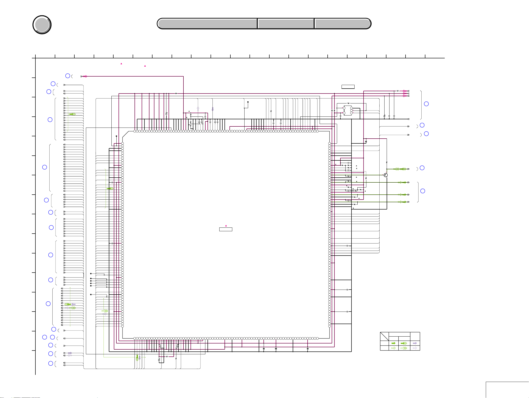
DSC-V1
COVER
COVER
For Schematic Diagram
• Refer to page 4-51 for printed wiring board.
1
32
SY-089 BOARD (4/12)
A
CAMERA DSP(HMS BLOCK)
XX MARK:NO MOUNT
NO MARK:REC/PB MODE
B
C
D
E
F
G
H
I
J
K
L
M
N
O
P
05
(1/12)
6
(1/12)
9
(2/12)
19
(3/12)
21
(5/12)
22
(5/12)
23
(5/12)
24
(5/12)
25
(5/12)
26
(5/12)
29
28
(10/12)
(5/12)
30
(10/12)
31
(8/12)
32
(7/12)
2
VSUB_CONT
XFC_RST_LED
XFC_RST_SENS
XZM_RST_SENS1
XZM_RST_SENS2
MSHUT_EN
MSHUT_ON
XLENS_RST_LED
XIR_SENS_LED
XIR_RST_SENS
IR_FILTER_IN
IR_FILTER_OUT
XCS_HMS_RAM
XCS_HMS_REG
MC_D00
MC_D01
MC_D02
MC_D03
MC_D04
MC_D05
MC_D06
MC_D07
MC_D08
MC_D09
MC_D10
MC_D11
MC_D12
MC_D13
MC_D14
MC_D15
27
(6/12)
TG_WEN
CA_AD00
CA_AD01
CA_AD02
CA_AD03
CA_AD04
CA_AD05
CA_AD06
CA_AD07
CA_AD08
CA_AD09
CA_AD10
CA_AD11
CA_AD12
CA_AD13
HR_EN0
HR_DIR0A
HR_DIR0B
HR_EN1
HR_DIR1A
HR_DIR1B
HR_EN2
HR_DIR2A
HR_DIR2B
AU_LRCK
MC_XWE0
MC_XWE1
MC_XRD
MC_A01
MC_A02
MC_A03
MC_A04
MC_A05
MC_A06
MC_A07
MC_A08
MC_A09
MC_A10
MC_A11
MC_A12
MC_A13
MC_A14
MC_A15
MC_A16
MC_A17
MC_A18
MC_A19
MC_A20
MC_A21
MC_A22
MC_A23
MC_A24
MC_A25
XRST_SYS
AU_AOUT
AU_AINL
PANEL_V
CLPDM
PLLBYP
IRQIMG
20
AU_2.9V
(8/12)
VSUB_CONT
XFC_RST_LED
XFC_RST_SENS
XZM_RST_SENS1
XZM_RST_SENS2
HR_DIR0A
HR_DIR0B
HR_DIR1A
HR_DIR1B
HR_DIR2A
HR_DIR2B
MSHUT_EN
MSHUT_ON
XLENS_RST_LED
XIR_SENS_LED
XIR_RST_SENS
IR_FILTER_IN
IR_FILTER_OUT
AU_LRCK
XCS_HMS_RAM
XCS_HMS_REG
MC_XWE0
MC_XWE1
XRST_SYS
AU_AOUT
TG_WEN
CA_AD00
CA_AD01
CA_AD02
CA_AD03
CA_AD04
CA_AD05
CA_AD06
CA_AD07
CA_AD08
CA_AD09
CA_AD10
CA_AD11
CA_AD12
CA_AD13
HR_EN0
HR_EN1
HR_EN2
PLLBYP
IRQIMG
MC_XRD
MC_A01
MC_A02
MC_A03
MC_A04
MC_A05
MC_A06
MC_A07
MC_A08
MC_A09
MC_A10
MC_A11
MC_A12
MC_A13
MC_A14
MC_A15
MC_A16
MC_A17
MC_A18
MC_A19
MC_A20
MC_A21
MC_A22
MC_A23
MC_A24
MC_A25
MC_D00
MC_D01
MC_D02
MC_D03
MC_D04
MC_D05
MC_D06
MC_D07
MC_D08
MC_D09
MC_D10
MC_D11
MC_D12
MC_D13
MC_D14
MC_D15
AU_AINL
PANEL_V
MCK12
CA_FD
CA_HD
CLPOB
CLPDM
CLPOB
CLPDM
CA_HD
CA_FD
CA_AD13
CA_AD12
CA_AD09
CA_AD11
CA_AD10
CA_AD08
CA_AD06
CA_AD07
CA_AD04
CA_AD05
CA_AD03
XWAIT
CKIO
SYS_V
HDO
CA_AD02
CA_AD00
CA_AD01
MC_A23
MC_A25
MC_A22
MC_A24
MC_A19
MC_A21
MC_A18
MC_A20
MC_A15
MC_A14
MC_A17
MC_A11
MC_A16
MC_A13
MC_A08
MC_A07
MC_A12
MC_A05
MC_A10
MC_A04
MC_A09
MC_A03
MC_A02
MC_A06
MC_A01
CL601
MC_XRD
CL602
XCS_HMS_REG
CL603
XCS_HMS_RAM
CL604
MC_XWE0
CL605
MC_XWE1
IRQIMG
CL606
XWAIT
MC_D09
MC_D02
MC_D00
MC_D08
MC_D13
MC_D05
MC_D01
MC_D04
MC_D07
MC_D12
MC_D15
MCK12
CA_FD
CA_HD
CLPOB
XWAIT
CKIO
SYS_V
HDO
4-2. SCHEMATIC DIAGRAMS
4-2. SCHEMATIC DIAGRAMS
56
:Voltage measurment of the CSP ICs
and the Transistors with mark,are
not possible.
291
292
293
294
295
296
297
298NC299NC300NC301NC302
303NC304
NC
CL607
C602
0.1u
C601
0.1u
NC
1
SMCK
2
CAMVDI
3
EXTVALID
4
DGND_0
5
PBLK
6
OPBCLP
7
DUMCLP
8
CCDHD
9
CCDFD
VCC3_0
10
ADIN15
11
ADIN13
12
ADIN12
13
ADIN09
14
ADIN14
15
ADIN11
16
VCC2_0
17
ADIN10
18
ADIN08
19
ADIN06
20
ADIN07
21
ADIN04
22
ADIN05
23
ADIN03
24
ADIN02
25
ADIN00
26
ADIN01
27
DGND_1
28
A23
29
A25
30
A22
31
A24
32
A19
33
A21
34
A18
35
A20
36
A15
37
A14
38
A17
39
A11
40
A16
41
VCC3_1
42
A13
43
A08
44
A07
45
A12
46
A05
47
A10
48
A04
49
A09
50
A03
51
A02
52
A06
53
A01
54
RDX
55
VCC2_1
56
CSX
57
CSXRAM
58
WRLX
59
WRHX
60
IRQJPG
61
IRQIMG
62
DGND_2
63
XWAIT
64
D09
65
D02
66
D00
67
D08
68
D13
69
VCC3_2
70
D05
71
D01
72
D04
73
D07
74
D12
75
D15
76
D1178D0379D0680D1481D1082DGND_383XWAITIN84MD[0]85MD[1]86MD[2]87PLLVCC88CLKI89PLLGND90PLLMD[0]91PLLINSEL92DACMD93VCC2_294RSTX95SONYTEST96CLKTG97PLLMD[1]98PLLMD[2]99PLLXMSK
77
MC_D03
MC_D11
MC_D06
MC_D14
VSSQR
MC_D10
VSSL
VSSR
VDDR
VSSQL
VDDQL
VDDQR
C604
0.01u
L601
C603
10uH
22u
4V
CKIO
813 20184
FB604
C606
22u
6.3V
284
285
283
286
287SM288
289
290
/cs
MST
XTST
VDDL
AVDD_3
DGND_16
0.1u
C607
R601
1k
MCK12
XRST_SYS
9
AU_AINL
R602
10k
0.5%
R603
5600
0.5%
C608
0.5%
R604
10k
280
281
278
279
282
VRPR
VRNR
AVS_2
AVS_3
AOUTR
VCC3_3
PLL24
PLL12
100
101
102
103
AU_AOUT
C610
0.1u
0.1u
0.1u
C609
275
276
277
VRBL
VRNL
AOUTL
VCC2_3
PLLBYP
104
105NC106
PLLBYP
AVDD_2
XCS00
0.1u
0.1u
0.1u
C613
C612
C611
268
269
270
271
272
273
274
AIN
VRL
VRH
VR_1
AVS_1
AVDD_1
DGND_4
107
XCS01
108
XCS02
XCS03
109
110
DGND_15
IC601
CAMERA DSP,256M SDRAM
IC601
(HM(5M SA)BOARD)
XRAS
XCAS
QCLKE
111
112
113
114
ACLK
VCC3_4
266NC267
115NC116
11
CL608
AU_LRCK
258
259
260
261
262
263
264
265
SCLK
AUCK
ADCK
XACLK
XPWAD
XPWDA
VCC3_14
QCLK
DGND_5
BA01
AQ09
BA00
VCC3_5
AQ12
122
117
123
118
119
120
121
SY-089 BOARD SIDE A SY-089 BOARD SIDE B
SY-089 BOARD SIDE A SY-089 BOARD SIDE B
127 15
MSHUT_ON
246
VCC3_13
AQ01
135
C616
0.1u
245
SHUTTER
VCC3_6
136
C617
0.1u
IRISOUT
AQ00
HR_EN2
HR_DIR1B
HR_DIR2A
HR_DIR2B
238
239
240
241
242
243
244
EN2
DIR1B
DIR2A
DIR2B
SENS2
VCC2_7
XWE
DQM03
DQM02
DQM01
DQM00
DGND_7
137
138
139
140
141
142
143
VCC2_8
AQ06
STRB_ON
VSUB_CONT
EXT_STRB_ON
R605
1k
C615
0.1u
247
248
249
250
251
252
253
254
255
256
257
SIA
SOA
VR_0
AVS_0
AVDD_0
STRBAD
AQ05
AQ11
AQ03
AQ10
124
125
126
127
STROBE1
STROBE2
SUBCNTL
DGND_14
DGND_6
AQ02
VCC2_4
AQ07
AQ08
AQ04
128
129
130
131
132
133
134
C614
0.1u
1410 19 21
HR_EN1
HR_EN0
DIR0B
DQ25
HR_DIR0A
234
147
DIR0A
DQ28
233
148
C618
0.1u
XFC_RST_SENS
232
EN0
SENS0
VCC3_7
DQ27
149
PANEL_V
230
229
231
VPD
LCDVD
VCC3_12
DGND_13
DGND_12
DGND_11
DGND_10
DQ23
DQ22
DQ26
151
152
150
HR_DIR1A
DIR1A
DQ30
HR_DIR0B
235
236
237
EN1
SENS1
DQ31
DQ29
145
144
146
CAMVDO
EXTPAL
VCC2_6
VCC3_11
VCC2_5
VCC3_10
VCC3_9
DGND_9
VCC3_8
DGND_8
16
FB603
FB602
228
NTVDO
227
FLD
226
HD
225
224
223
NC
222
VAVS4
221
R607
27k
CO
220
0.5%
VAVD4
219
VRO2
218
VREF2
217
VAVD3
216
YO
215
VAVS3
214
VAVS2
213
RO
212
VAVD2
211
VRO1
210
VREF1
209
VAVD0
208
GO
207
BAVS0
206
BAVD1
205
C619
BO
204
VAVS1
203
202
PIO00
201
200
PIO05
199
PIO01
198
PIO06
197
PIO02
196
PIO03
195
PIO09
194
193
PIO10
192
PIO04
191
PIO12
190
PIO07
189
PIO08
188
PIO13
187
186
PIO14
185
PI011
184
PIO15
183
182
DQ00
181
DQ02
180
179
DQ03
178
DQ01
177
DQ06
176
DQ04
175
DQ07
174
DQ05
173
172
DQ09
171
DQ08
170
DQ10
169
168
DQ12
167
DQ11
166
165
DQ13
164
DQ14
163
DQ16
162
DQ17
161
DQ18
160
159
DQ15
158
DQ19
157
DQ20
156
DQ21
155
154
DQ24
153
2.9
C635
XX
R606
C622 0.1u
C623
IC602
TC7S86FU(TE85R)
0
10k
0.1u
0.1u
45
Y GND
VCC
17
L602
XOR
IC602
R622
XX
XZM_RST_SENS1
2.8
A
2.8
123
B
C620
18k
6800
C621
330
560
0.5%
R614
R608
C633
XX
C634
0.1u
XZM_RST_SENS2
STRB_ON
EXT_STRB_ON
C624
XX
SYS_V
HDO
0.1u
R609
0.5%
R610
0.5%
XX
R611
0.5%
R612
0.5%
18k
R615
0.5%
27k
0.5%
R613
560
0.5%
560
0.5%
R616
XX
IR_FILTER_OUT
XLENS_RST_LED
IR_FILTER_IN
MSHUT_EN
XFC_RST_LED
XFC_RST_SENS
XIR_SENS_LED
XZM_RST_SENS2
XIR_RST_SENS
XZM_RST_SENS1
TG_WEN
0.2
SIGNAL PATH
10uH
A_2.9V
D_2.9V
D_1.5V
33
(12/12)
Y/CHROMA
REG_GND
STRB_ON
EXT_STRB_ON
CV_OUT
PANEL_R
PANEL_G
PANEL_B
AUDIO
SIGNAL
(11/12)
34
35
(12/12)
36
(8/12)
37
(7/12)
C626
C627
C625
10u
10u
22u
4V
R620
2200
0.8
Q606
2SA2029T2LQ/R
BUFFER
VIDEO SIGNAL
CHROMA
REC
PB
4-15
4-16
SY-089 (4/12)
Page 23

DSC-V1
COVER
COVER
For Schematic Diagram
• Refer to page 4-51 for printed wiring board.
1
SY-089 BOARD (5/12)
A
SH DSP(SH BLOCK 1/2)
XX MARK:NO MOUNT
NO MARK:REC/PB MODE
B
38
(12/12)
C
D
39
E
(11/12)
PRELAMP_AF_ON
F
40
(12/12)
G
(6/12)
41
H
42
(10/12)
I
17
(3/12)
J
XAU_POWER_SAVE
43
(8/12)
K
REG_GND
USB_3.2V
IR_LED_ON
HSHOE_CONT
EXT_STRB_CONT
TG_CLK_EN
USB_CLK_EN
XAE_LOCK_LED
XMC_NMI
MC_HELP
MC_UPDATE
DAC_STB
XCAM_DR_PS
LENS_TEMP
AU_HGL_SEL
XAU_SP_MUTE
XAU_LINE_MUTE
VAMP_ON
D_2.9V
PD_LEV
XCS_MC
D_1.5V
2
C501
10u
CL501
XRST_JTAG
CL502
XASEMD0
CL503
XASEBREAK
CL504
XTRST
R501
TCK
TDI
TDO
TMS
XEEPROM_BUSY
DAC_STB
MS_POWER_ON
VBUS
MC_D15
MC_D14
MC_D13
MC_D12
MC_D11
MC_D10
MC_D09
MC_D08
MC_D07
MC_D06
MC_D05
MC_D04
MC_D03
MC_D02
MC_D01
MC_D00
XCS_MC
XMC_NMI
MC_HELP
MC_UPDATE
DAC_STB
XCAM_DR_PS
LENS_TEMP
AU_HGL_SEL
CL505
CL506
CL507
CL508
CL509
L
SIGNAL PATH
M
VIDEO SIGNAL
Y/CHROMA
AUDIO
SIGNAL
REC
PB
N
05
4-2. SCHEMATIC DIAGRAMS
4-2. SCHEMATIC DIAGRAMS
4 118 15
C502
47u
4V
0
2.6
Q501
DTC144EMT2L
LED DRIVE
0
5
:Voltage measurment of the CSP ICs
and the Transistors with mark,are
not possible.
FB505
FB506
RB501
47k
0.1u
C503
0.1uC504
47k
R503
1
STATUS1/PTE(1)
2
STATUS0/PTE(0)
3
XVDATA/PTD(0)
4
TXENL/PTD(1)
5
SUSPND/PTD(1)
6
VBUS/PTD(3)
7
T02/PTQ(1)
8
TO0/PTE(2)
9
BREQ
TO3/PTQ(2)
10
TXDMNS/PTD(7)
11
TXDPLS/PTD(6)
12
PTM(2)
13
DPLS/PTD(4)
14
DMNS/PTD(5)
15
TEND/PTQ(0)
16
D31/PTB(7)
17
Vcc
18
D30/PTB(6)
19
Vss
20
D29/PTB(5)
21
D28/PTB(4)
22
D27/PTB(3)
23
VssQ
24
D26/PTB(2)
25
VccQ
26
D25/PTB(1)
27
D24/PTB(0)
28
PTM(1)
29
D23/PTA(7)
30
D22/PTA(6)
31
D21/PTA(5)
32
D20/PTA(4)
33
D19/PTA(3)
34
D18/PTA(2)
35
D17/PTA(1)
36
D16/PTA(0)
37
VssQ
38
D15
39
VccQ
40
D14
41
D13
42
D12
43
D11
44
D10
45
Vcc
46
D9
47
Vss
48
D8
49
PTM(0)
50
D7
51
D6
52
VssQ
53
D5
54
VccQ
55
D4
56
D3
57
D2
58
D1
59
D0
60
6
RB504
47k
C522
0.1u
C507
0.1u
235
236
237
238
239DP240
DM
AVss
AVcc(USB)
AN[7]/PTL[7]
VssQ
A0/PTK(0)62A1
63A264A365
61
MC_A01
MC_A02
MC_A03
7
CCD_TEMP
LENS_TEMP
RB505
0.1uC508
228
229
230
231
232
233
234
AN[6]/PTL[6]
66A467
MC_A04
AVcc(AD)
AN[1]/PTL[1]
AN[2]/PTL[2]
AN[3]/PTL[3]
AN[4]/PTL[4]
AN[5]/PTL[5]
VccQ68A569A670A771PTN(6)72A873A974TI2A/PTN(7)75A1076A11
MC_A05
MC_A06
MC_A07
XEEPROM_WE
MC_A08
XFE_CS
RB503
1k
47k
0.1u
CL510
C509
221
222
223
224
225
226
227
PTM(3)
AVss(AD)
TO1/PTE(3)
AN[0]/PTL[0]
CTS5/SCPT2(6)
TXD5/SCPT2(4)
RTS5/SCPT2(5)
RXD5/SCPT2(4)
TI2B/PTQ(7)78A1279A1380VssQ81A1482VccQ83A1584A1685A1786A1887A19/PTK(1)88A20/PTK(2)
77
MC_A09
MC_UPDATE
MC_A10
MC_A11
MC_A12
MC_A13
XCAM_RESET
CL511
219
220
PTM(4)
MC_A14
C511
0.1u
218
VccQ
0.1u
C510
MC_A15
SY-089 BOARD SIDE A SY-089 BOARD SIDE B
SY-089 BOARD SIDE A SY-089 BOARD SIDE B
CKIO2
217
MC_A16
XACCESS_LED
216
VssQ
MSDIR/PTC(0)
MC_A17
MS_DIO
215
MSDIO/PTC(1)
MC_A18
9
MS_BS
214
MSBS/PTC(2)
MC_A19
MS_SCLK
FB504
100
R519
212
213
Vcc
MSSCLK/PTC(3)
IC501
MC CAM,SH DSP,FLASH
HD6417190BPZ110CHV
Vss90A21/PTK(3)91Vcc
89
MC_A20
XFLASH_WP
211
PTM(5)
IC501
MC_A21
XUSB_DACK1
209
210
DACK1/PTC(7)
0.1u
C512
92
MC_A22
10
EEPROM_SCK
XUSB_DREQ1
204
205
206
207
208
Vss
TXD3/PTH(5)
SCK3/PTH(7)
SCK2/PTH(4)
RXD3/PTH(6)
DREQ(1)/PTC(6)
A22/PTK(4)93A23/PTK(5)94VssQ95A24/PTK(6)96VccQ97A25/PTK(7)98BS
MC_A23
MC_A24
MC_A25
EEPROM_SI
203
RXD2/PTH(3)
EEPROM_SO
202
TXD2/PTH(2)
99RD100
MC_XRD
CAM_SI
201
RXD1/SCPT(5)
WE0/DQMLL
MC_XWE0
CAM_SO
R543 100k
200
TXD1/SCPT(4)
WE1/DQMLU
101
MC_XWE1
XCAM_SCK
199
SCK1/SCPT(6)
WE2/DQMUL
102
CAM_DD_ON
197
198
PTM(6)
WE3/DQMUU/AH
103
104
195
196
SCK4/SCPT2(1)
RXD4/SCPT2(0)
TI3A/PTQ(6)
RDWR
106
105
CL512
193
194
CTS4/SCPT2(3)
RTS4/SCPT2(2)
TXD4/SCPT2(0)
AUDSYNC/PTG(4)
TI3B/PTQ(5)
VssQ
107
108
FR_SO
XCAM_DR_PS
191
192
PTM(7)
CS0
109
110
XCS_FLASH
XTG_CS
12
FR_SI
190
TXD0/SCPT(0)
RXD0/SCPT(0)
PTN(5)
VccQ
111
XEEPROM_CS
188
189
PTN(0)
CS2/PTJ(0)
112
113
CKIO
186
187
CKIO
VccQ
CS3/PTJ(1)
CS4/PTJ(2)
114
115
XCS_HMS_RAM
185
VssQ
CS5A/PTJ(3)
116
FR_SCK
184
SCK0/SCPT(2)
CS5B/PTJ(4)
117
XCS_HMS_REG
13
182
183
MD0
UCLK/PTH(0)
CS6A/PTJ(5)
CS6B/PTJ(6)
118
119
XCS_USB
181
MD2
MD1
Vcc(PLL2)
Vss(PLL2)
Vss(PLL1)
Vcc(PLL1)
IRQ4/PTF(4)
IRQ3/PTF(3)
IRQ2/PTF(2)
IRQ1/PTF(1)
IRQ0/PTF(0)
SCL(O/D)/PTF(6)
SDA(O/D)PTF(7)
AUDATA(0)/PTG(0)
AUDATA(1)/PTG(1)
IRQ7/PTQ(4)
AUDATA(2)/PTG(2)
AUDATA(3)/PTG(3)
IRQ6/PTQ(3)
TCLK/PTJ(7)
ASEBREKAK/PTG(5)
ASEMD0
SCS0/SCPT(3)
DACK0/PTC(5)
DREQ0/PTC(4)
IRQ5/PTF(5)
RASU/PTE(5)
CASU/PTE(7)
CASL/PTE(6)
RASL/PTE(4)
CKE/PTH(1)
VccQ
MD3
120
AUDCK
PTN(1)
PTN(2)
PTN(3)
RESETP
RESETM
PTN(4)
EXTAL
VccQ
180
179
XTAL
178
VssQ
177
176
CAP2
175
174
173
CAP1
172
171
Vss
170
169
168
167
166
165
164
Vcc
163
162
Vss
161
160
TCK
159
TDI
158
157
TMS
156
TRST
155
154
153
152
151
150
149
148
VccQ
147
146
VssQ
145
144
143
VccQ
142
141
140
139
WAIT
138
137
NMI
136
Vcc
135
134
Vss
133
BACK
132
TDO
131
130
129
128
VccQ
127
126
VssQ
125
124
123
122
121
C515
0.1u
C513 0.1u
R525 XX
R527 XX
MC_XWE0
MC_XWE1
173 14
XCS_PANEL_TG
CAM_SI
CAM_SO
XCAM_SCK
XCAM_RESET
XTG_CS
XFE_CS
CCD_TEMP
CAM_DD_ON
FR_SI
FR_SO
FR_SCK
XRST_SYS
SYS_V
PLLBYP
AU_LRCK
IRQIMG
XWAIT
XCS_HMS_RAM
XCS_HMS_REG
CKIO
EEPROM_SI
EEPROM_SO
EEPROM_SCK
XEEPROM_CS
XEEPROM_WE
XEEPROM_BUSY
VBUS
XCS_USB
XUSB_DREQ0
XUSB_DACK0
XUSB_DREQ1
XUSB_DACK1
XUSB_IRQ
MC_XWE0
MC_XWE0
MC_XWE1
XCS_FLASH
XFLASH_WP
MC_XWE1
MC_XRD
MC_A01
MC_A02
MC_A03
MC_A04
MC_A05
MC_A06
MC_A07
MC_A08
MC_A09
MC_A10
MC_A11
MC_A12
MC_A13
MC_A14
MC_A15
MC_A16
MC_A17
MC_A18
MC_A19
MC_A20
MC_A21
MC_A22
MC_A23
MC_A24
MC_A25
MC_D00
MC_D01
MC_D02
MC_D03
MC_D04
MC_D05
MC_D06
MC_D07
MC_D08
MC_D09
MC_D10
MC_D11
MC_D12
MC_D13
MC_D14
MC_D15
3
(1/12) (2/12)
(1/12)11(2/12)
(1/12)
46
(10/12)
47
(10/12)
28
(4/12)
XACCESS_LED
MS_POWER_ON
MS_BS
MS_DIO
MS_SCLK
(9/12)
(4/12)
51
(6/12)
23
(4/12)
(4/12)24(6/12)
25
(4/12)
26
(4/12)
44
(7/12)
4
7
21
(4/12)
49
(6/12)
50
22
52
(6/12) (9/12)
53
(6/12)
16 18
XCS_PANEL_TG
CAM_SI
CAM_SO
XCAM_SCK
XCAM_RESET
XTG_CS
XFE_CS
CCD_TEMP
CAM_DD_ON
FR_SI
FR_SO
FR_SCK
XRST_SYS
SYS_V
C516
0.1u
L502
10uH
C517
22u
4V
CL514
IRQIMG
SYS_V
PLLBYP
TCK
MC_HELP
TMS
XTRST
XUSB_IRQ
AU_LRCK
XASEBREAK
XASEMD0
XWAIT
XCS_PANEL_TG
XMC_NMI
XCS_MC
TDO
XUSB_DACK0
XUSB_DREQ0
RB502
47k
AU_HGL_SEL
XRST_JTAG
C518
0.1u
XRST_SYS
R533
1k
PLLBYP
AU_LRCK
IRQIMG
XWAIT
XCS_HMS_RAM
XCS_HMS_REG
XACCESS_LED
MS_POWER_ON
MS_BS
MS_DIO
MS_SCLK
CKIO
EEPROM_SI
EEPROM_SO
EEPROM_SCK
XEEPROM_CS
XEEPROM_WE
XEEPROM_BUSY
VBUS
XCS_USB
XUSB_DREQ0
XUSB_DACK0
TDI
XUSB_DREQ1
XUSB_DACK1
XUSB_IRQ
XCS_FLASH
XFLASH_WP
MC_XRD
MC_A01
MC_A02
MC_A03
MC_A04
MC_A05
MC_A06
MC_A07
MC_A08
MC_A09
MC_A10
MC_A11
MC_A12
MC_A13
MC_A14
MC_A15
MC_A16
MC_A17
MC_A18
MC_A19
MC_A20
MC_A21
MC_A22
MC_A23
MC_A24
MC_A25
MC_D00
MC_D01
MC_D02
MC_D03
MC_D04
MC_D05
MC_D06
MC_D07
MC_D08
MC_D09
MC_D10
MC_D11
MC_D12
MC_D13
MC_D14
MC_D15
10 13
(3/12) (7/12)
48
(6/12)
55
54 56
(9/12)
19
45
SY-089 (5/12)
4-17 4-18
Page 24

DSC-V1
COVER
COVER
For Schematic Diagram
• Refer to page 4-51 for printed wiring board.
• Refer to page 4-65 for waveforms.
1
SY-089 BOARD (6/12)
A
MEMORY,CLOCK GENERATOR(SH BLOCK 2/2,GEN BLOCK,CN1 BLOCK 1/4)
XX MARK:NO MOUNT
NO MARK:REC/PB MODE
D_2.9V
A_2.9V
2
4 1183
B
57
(12/12)
C
41
(5/12)
REG_GND
TG_CLK_EN
USB_CLK_EN
D
E
XEEPROM_CS
EEPROM_SCK
EEPROM_SO
EEPROM_SI
F
2.9
1
CS
2.9
2
SCK
0
3
DI
2.9
4
DO
BR9016ARFVM-WTR
IC502
EEPROM
IC502
BUSY
VCC
RST
GND
G
58
XMS_IN
(10/12)
H
XACCESS_LED
MS_POWER_ON
48
I
(5/12)
J
MS-165
FLEXIBLE
LND001-LND008
(PAGE 4-40)
59
(10/12)
MS_BS
MS_DIO
MS_SCLK
STATIC_GND
R718
180
D706
MA2S111-(K8).SO
D703
8PCN705
8
VSS
7
VCC
6
SCLK
5
INT
4
DIO
3
NC
2
BS
1
VSS
R719
0
D707
MAZS082008S0
K
05
4-2. SCHEMATIC DIAGRAMS
4-2. SCHEMATIC DIAGRAMS
5 12
:Voltage measurment of the CSP ICs
and the Transistors with mark,are
not possible.
FB581
2.9
8
2.9
7
2.9
6
5
D704
CL-270HR-C-TS
(MS ACCESS)
MA2SD24008S0
C524
0.1u
SSM6E01TU
2.9 2.9
C704
0.1u
C703
22u
6.3V
R539
Q704
B+ SWITCH
0
R708
2200
XX
XEEPROM_BUSY
XEEPROM_WE
R710
680
4
5
1
2
2.9
XX
FB582
C581
10u
MC_A17
MC_A20
MC_A08
MC_A11
MC_A16
MC_A19
MC_D09
MC_A09
MC_A12
MC_A15
MC_A18
MC_A21
R707
470k
3
6
0
R709
3300
C702
0.47u
C582
XX
X581
27MHz
FB507
C584
0.1u
2.9
1
VDD
1.4
2
FIN
3
VSS
1.3
TCLK
4
2.9
5
T_ON
2.9
6
T_SEL0
7
T_SEL2
2.9
8
VDD
IC581
CLOCK GENERATOR
CY27030ZCT
MC_A13
MC_A10
MC_D07
A8
A11
VCC
DQ7
DQ26
NC
H5H6H7H8H9
A15
A18
DQ24
VCC
DQ22
J1J2J3J4J5J6J7J8J9K2K3K4K5K6
DQ23
A6
A9
NC
A14
A17
VCC
DQ9
VSS
A7
A10
NC
A13
A16
K7K8
A19
WE
A4
NC
A1
MC_A03
NC
R521
MC_XWE1
A3 A4 A5 A6 A7 A8 B2 B3
C519
10u
MC_A06
SY-089 BOARD SIDE A SY-089 BOARD SIDE B
SY-089 BOARD SIDE A SY-089 BOARD SIDE B
967
1.4
REF
123
IC581
VSS
DQ25
MBM29PL3200BE90PBT-62-ER
VCC
CE
XX
XCS_FLASH
16
VSS
15
2.9
T_SEL1
14
0
U_ON
13
2.9
VDD
12
0
UCLK
11
VSS
10
2.9
9
U_SEL
MC_D06
MC_A14
MC_D08
G6G7G8G9H1H2H3H4
NC
A12
DQ6
DQ8
DQ21
IC503
32M FLASH
IC503
DW/W
NC
ACC
A2
A5
B4 B5 B6 B7 B8 B9 C1 C2 C3 C4 C5 C6 C7
CL513
MC_A04
MC_A07
10
R581
R584
0
22
R585
R582
0
22
R586
R583
22
0
MC_D00
NC
DQ0
NC
A3
MC_A05
MC_D05
NC
WP
XFLASH_WP
DQ5
NC
MC_D04
F2F3F4F5F6F7F8F9G1G2G3G4G5
DQ4
OE
MC_XRD
DQ31/A-1
DQ20
DQ12
DQ28
VSS
NC
NC
DQ2
DQ18
DQ19
DQ3
DQ13
DQ29
DQ14
NC
A0
DQ16
VSS
VCC
VCC
DQ15
MC_D11
MC_D10
VSS
DQ27
DQ10
DQ11
DQ17
DQ30
VSS
DQ1
MC_D01
SIGNAL PATH
VIDEO SIGNAL
Y/CHROMA
AUDIO
SIGNAL
REC
PB
13
USB_CLK
TG_CLK
EEPROM_SI
EEPROM_SO
EEPROM_SCK
XEEPROM_CS
XEEPROM_WE
XEEPROM_BUSY
XCS_FLASH
XFLASH_WP
MC_XWE1
MC_XRD
MC_D12
MC_A01
MC_A02
MC_A03
MC_D02
MC_D03
MC_D13
MC_D14
MC_A01
MC_A02
MC_D15
MC_A04
MC_A05
MC_A06
MC_A07
MC_A08
MC_A09
MC_A10
MC_A11
MC_A12
MC_A13
MC_A14
MC_A15
MC_A16
MC_A17
MC_A18
MC_A19
MC_A20
MC_A21
MC_D00
MC_D01
MC_D02
MC_D03
MC_D04
MC_D05
MC_D06
MC_D07
MC_D08
MC_D09
MC_D10
MC_D11
MC_D12
MC_D13
MC_D14
MC_D15
E6 E7 E8 E9 F1
D1 D2 D3 D4 D5 D6 D7 D8 D9 E1 E2 E3 E4 E5
C8 C9
C520
0.1u
EEPROM_SI
EEPROM_SO
EEPROM_SCK
XEEPROM_CS
XEEPROM_WE
XEEPROM_BUSY
XCS_FLASH
XFLASH_WP
MC_XWE1
MC_XRD
MC_A01
MC_A02
MC_A03
MC_A04
MC_A05
MC_A06
MC_A07
MC_A08
MC_A09
MC_A10
MC_A11
MC_A12
MC_A13
MC_A14
MC_A15
MC_A16
MC_A17
MC_A18
MC_A19
MC_A20
MC_A21
MC_D00
MC_D01
MC_D02
MC_D03
MC_D04
MC_D05
MC_D06
MC_D07
MC_D08
MC_D09
MC_D10
MC_D11
MC_D12
MC_D13
MC_D14
MC_D15
14
27
CKIO
(4/12)
60
(9/12)
5
(1/12)
CKIO
49
(5/12)
51
(5/12)
52
(5/12)
53
(5/12)
54
(5/12)
4-19
4-20
SY-089 (6/12)
Page 25

DSC-V1
COVER
COVER
For Schematic Diagram
• Refer to page 4-51 for printed wiring board.
• Refer to page 4-65 and 4-66 for waveforms.
1
SY-089 BOARD (7/12)
A
LCD DRIVE,TIMING GENERATOR(PD BLOCK,CN1 BLOCK 2/4)
XX MARK:NO MOUNT
NO MARK:REC/PB MODE
PANEL_13.5V
PANEL_2.9V
61
B
(12/12)
REG_GND
C
PANEL_B
37
D
E
(4/12)
44
(5/12)
(5/12)
45
PANEL_G
PANEL_R
XCS_PANEL_TG
CAM_SI
CAM_SO
XCAM_SCK
XCS_PANEL_TG
XCAM_SCK
F
PANEL_V
32
(4/12)
62
(10/12)
XRST_SYS
HDO
XRST_SYS
G
SIGNAL PATH
VIDEO SIGNAL
CHROMA
REC
H
05
PB
CAM_SI
CAM_SO
PANEL_V
HDO
L802
C820
6.3V
4-2. SCHEMATIC DIAGRAMS
4-2. SCHEMATIC DIAGRAMS
482
C808
0.1u
R823
0
C809
0.01u
VDD
37
2.9
BIN
38
1.7
39
GIN
1.7
RIN
40
1.7
SCAN
41
42
XVD
2.8
HD
43
2.6
VCC1
44
2.8
XCS
45
2.8
XSCK
46
2.8
SI
47
1.2
SO
48
2.7
C807
XX
C806
0.01u
C802
0.1u
10u
10uHL803
47uH
47u
C819
0.01u
C805
PANEL_V
HDO
XCS_PANEL_TG
XCAM_SCK
CAM_SO
CAM_SI
XRST_SYS
5 12
EN
VST
VCK
DWN
C810
2.2u
25V
0
1.4
35
36
VST
VCK
VSS
BL_ON
2.6
2.9
2.8
31
32
33EN34
DWN
PWM
2.8
30
BLDET
2.5
29
FBACK
BL_LEV
2.5
28
EXTDA
13.6
7
25
26
27
VP
XLED
VCC3
9
4
5
6
7
8
XWRT/CLKIN2RGT3HCK14HCK25HDO6REF7OP_OUT8OP_IN9XCLR10Filter211Filter12VSS
1
2.9
1.8
HCK1
RGT
1.8
JL801
HCK2
IC801
LCD DRIVE,
TIMING GENERATOR
IC801
CXA3622AR-T4
1.4
1.2
REF
R808
1.4
2.9
1.3
R807
XX
560pC812
C811
68k
0.1u
10
11
12
1.1
R809
R810
100k
SY-089 BOARD SIDE A SY-089 BOARD SIDE B
SY-089 BOARD SIDE A SY-089 BOARD SIDE B
910
VP
NC
24
6.5
COM
23
13.6
VCC2
10k
0.5%
0.5%
GND2
GND1
XPOFF
WIDE
HST
VDD
22
7.1
VB
21
7.1
20
VG
7.1
VR
19
18
17
0
16
0.2
15
0
14
2.9
13
JL802
RB801
10
VB
VG
VR
XPOFF
WIDE
HST
UP04601008S0
BL_LEV
BL_ON
VG
VR
VB
VP
7
Q801
PSIG DRIVE
XPOFF
C813
4.7u
Q802
UP04601008S0
PSIG DRIVE
R815
47k
6.5
2
6
VST
VCK
EN
DWN
WIDE
HST
REF
HCK2
HCK1
RGT
7
1
4
13.6
R816
5
3
R817
470k
10k
R818
47k
7.6
7
113
Q803
MCH3310-TL-E
B+ SWITCH
C814
0.1u
46
3
1
6.5
5
1367
13.613.6
C815
0.01u
0.3
24PCN801
TEST1
1
COM
2
VST
3
VCK
4
EN
5
DWN
6
VDD
D801
MA8036-TX
C816
1u
R819
150k
13.6
7.6
2
7
C817
7
VSS
8
9
VDDG
VSSG
10
CS
11
WIDE
12
HST
13
REF
14
SOUT
15
0.1u
JL803
16
17
18
19
20
21
22
23
24
1
2
3
4
5
6
CN702
CRext
HCK2
HCK1
PSIG
G
R
B
RGT
TEST2
BL_THL
N.C
BL_THH
BL_L
N.C
BL_H
6P
BL_THH
BL_THL
BL_H
BL_L
BL_LEV
BL_ON
63
(12/12)
14
PANEL UNIT
LCD901
COLOR
LCD
MONITOR
D901
BACKLIGHT
SY-089 (7/12)
The components identified by mark 0 or dotted
line with mark 0 are critical for safety.
Replace only with part number specified.
4-21 4-22
Les composants identifiés par une marque 0 sont
critiques pour la sécurité. Ne les remplacer que
par une piéce portant le numéro spécifié.
Page 26

DSC-V1
COVER
COVER
For Schematic Diagram
• Refer to page 4-51 for printed wiring board.
• Refer to page 4-66 for waveforms.
1
2
SY-089 BOARD (8/12)
A
AUDIO,VIDEO(AU BLOCK,VI BLOCK)
XX MARK:NO MOUNT
NO MARK:REC/PB MODE
B
C
C202
R202
4.7u
47k
1u
D
E
F
C204
C201
0.01u
C203
0.015u
R203
2700
C206
C205
0.015u
R204
10k
0.1u
NC(HK)
J9
NC(HN)
G7
STBY
H9
LPF_SEL
G8
AGC_DET
G9
WHPF_OUT
F8
WHPF_BIAS
F9
WHPF_IN
E8
GAIN_SET
E9
MIC_OUT
D8
GND
D9
LINE_MUTE
C8
MIC_OFF
C9
MIC_IN
B8
NC
B3
4-2. SCHEMATIC DIAGRAMS
4-2. SCHEMATIC DIAGRAMS
4 1183
C208
0.015u
C211
0.01u
R206
1500
D2
A9
XX
R207
J8
NC
NC(HK)C7NC(HN)B9MIC_SPYA8MIC_2VB7MIC_REBA7VREFB6VCCA6MUTE_TMGB5GNDA5MUTE_DRVRB4LINE_OUTA4VCC_SPA3VCC_SPB2SP_SAVE
J6
AGC_OUT
C212
0.033u
0.022uC213
J5
H6
LPF1AH7LPF1BJ7LPF2AH8LPF2B
LPF_OUT
IC201
AUDIO AMP
IC201
AN12908A-VB
5
J4
H5
REC_OUT
REC_AMP_IN
:Voltage measurment of the CSP ICs
and the Transistors with mark,are
not possible.
C216
0.47u
C218
C217
1u
H3
J3
H4
AGND
PB_IN
VOL_CTL
SPAGC_SW
XX
G3
J1
NC(HN)
C220
10u
6.3V
R208
10k
NC(HK)
SPAGC_DET
XAUDIO_MUTE
SP_LPF_0
BEEP_OUT
BEEP_MIX_IN
XBEEP_MUTE
VREF_SP
SP_OUT-
SP_GND
SP_OUT+
6
AGND
BEEP
NC(HN)
NC(HK)
SY-089 BOARD SIDE A SY-089 BOARD SIDE B
SY-089 BOARD SIDE A SY-089 BOARD SIDE B
R211
2700
L201
10uH
10uH
9
68kR212
L202
7
C223
1u
C225
NC
C2
J2
H1
H2
G1
G2
F1
F2
E1
E2
D1
C1
A2
C3
A1
R209
4.7u
47k
C224
C219
0.001u
0.47u
1u
C221
XXC231
C232
0.047u
10V
C229
C228
C230
0.47u
10u
6.3V
XX
10
AU_AOUT
AU_AINL
XAU_POWER_SAVE
AU_HGL_SEL
XAU_SP_MUTE
XAU_LINE_MUTE
VAMP_ON
SP_VOL
BEEP_ON
BEEP
AU_2.9V
A_2.9V
CAM_P_5V
31
(4/12)
43
(5/12)
16
(3/12)
66
(10/12)
20
(4/12)
67
(12/12)
1u
1u
MIC_SIG
64
(11/12)
G
H
65
(12/12)
36
(4/12)
REG_GND
SP-
SP+
CV_OUT
C207
6.3V
10u
C209
C210
1u
C214
C215
1u
REG_GND
L101
10uH
C102
XX
22u
4V
C101
C103
R101
10u
1M
13
SIGNAL PATH
VIDEO SIGNAL
I
Y/CHROMA
REC
PB
AUDIO
SIGNAL
IC101
VIDEO AMP
IC101
NJM2574RB1(TE2)
J
05
2.8
2.9
8
CL/BI SW
LPF/THR SW
1
2.9
7
PowerSave
GND
2
6
Video-in
Vsag
3
2.9
5
1.6
VCC
14
V-OUT
C107
4
100u
1.1
1.1
R102
4V
C104
68
22u
4V
V_OUT
AU_OUT
68
(9/12)
4-23
4-24
SY-089 (8/12)
Page 27

DSC-V1
COVER
COVER
For Schematic Diagram
• Refer to page 4-51 for printed wiring board.
1
2
SY-089 BOARD (9/12)
A
USB INTERFACE(USB BLOCK,CN2 BLOCK 1/2)
XX MARK:NO MOUNT
70
55
(5/12)
56
(5/12)
60
(6/12)
USB_3.2V
REG_GND
XCS_USB
XUSB_DREQ0
XUSB_DACK0
XUSB_DREQ1
XUSB_DACK1
XUSB_IRQ
MC_XWE0
MC_XRD
MC_A01
MC_A02
MC_A03
MC_A04
MC_A05
MC_A06
MC_A07
MC_D00
MC_D01
MC_D02
MC_D03
MC_D04
MC_D05
MC_D06
MC_D07
MC_D08
MC_D09
MC_D10
MC_D11
MC_D12
MC_D13
MC_D14
MC_D15
XRST_SYS
USB_CLK
VBUS
XCS_USB
XUSB_DREQ0
XUSB_DACK0
XUSB_DREQ1
XUSB_DACK1
XUSB_IRQ
MC_XWE0
MC_XRD
MC_A01
MC_A02
MC_A03
MC_A04
MC_A05
MC_A06
MC_A07
MC_D00
MC_D01
MC_D02
MC_D03
MC_D04
MC_D05
MC_D06
MC_D07
MC_D08
MC_D09
MC_D10
MC_D11
MC_D12
MC_D13
MC_D14
MC_D15
XRST_SYS
VBUS
B
69
(12/12)
C
D
50
(5/12)
E
F
G
H
(10/12)
I
J
MC_XWE0
XCS_USB
MC_A02
MC_A06
MC_A04
MC_D09
10uH
L901
C905
0.01u
CL901
4-2. SCHEMATIC DIAGRAMS
4-2. SCHEMATIC DIAGRAMS
4 118 153
FB901
C901
10u
6.3V
C902
10u
6.3V
5 12
:Voltage measurment of the CSP ICs
and the Transistors with mark,are
not possible.
MC_A05
MC_D10
MC_D12
MC_D14
RB901
C906
MC_D05
C907
0.1u
D6
D13
VDD
GND
INT0B
84858687888990
WRB
0.1uC904
10k
0.1u
0.1uC903
SCAN1
VDD
GND
LD0
LD3
LD6
919293949596979899100101102
LD4
GND
VDD
GND
RPU
DP
GND
DM
PVDD
VDD
GND
CSB
103104105106107108109
A2
A6
A4
D1
VDD
GND
N.CD8D10
D12
12345678910111213141516171819202122232425262728
CL902
MC_D00
MC_D02
MC_D04
MC_D07
XUSB_IRQ
R911
9100
0.5%
0.1u
C908
A5
D2
D4
GND
INTB_ALL
D15
ACTIVE
INT1BM2GND
RB902
10k
M0
N.C
GND
XOUT
IC901
USB INTERFACE
UPD720122F1-DN1-E2-A
FM21
N.C
EP1_DACKB
EP1_TCB
CL903 CL904
XUSB_DACK0
GND
GND
IC901
EP2_TCB
EP2_DACKB
XUSB_DACK1
PVSS
LD2
RSDM
GND
GND
RREF
AVDD
LD7
LD11
LD9
SY-089 BOARD SIDE A SY-089 BOARD SIDE B
SY-089 BOARD SIDE A SY-089 BOARD SIDE B
10
LD8
AVSS(R)
LD5
AVSS
LD1
RSDP
56575859606162636465666768697071727374757677787980818283
RB905
10k
EP2_WRB
VDD
EP2_DRQB
EP1_RDB
EP1_DRQB
SCAN0
INT2B
XIN_CLK
RESETB
VBUS
C910
0.1u
XUSB_DREQ1
R924
CL905
CL906
CL907
R925
36
0.5%
0.5%
36
XUSB_DREQ0
MC_XRD
MC_D06
MC_D03
MC_D01
MC_D15
MC_D13
MC_D11
MC_D08
MC_A07
MC_A03
MC_A01
XRST_SYS
R927
1500
0.5%
VBUS
N.C
RDB
D14
D11
D9
N.C
D7
D5
D3
D0
A7
A3
A1
GND
N.C
M1
VDD
N.C
N.C
C911
29 30 31 32 33 34 35 36 37 38 39 40 41 42 43 44 45 46 47 48 49 50 51 52 53 54 55
0.1u
0.01u
C909
N.C
LD13
RB903
10k
RB904
LD12
LD14
LD10
N.C
LD15
BUNRI
10k
SIGNAL PATH
D756
MAZT082H08S0
REC
PB
13
D755
MAZT082H08S0
VIDEO SIGNAL
Y/CHROMA
XX
D753
R765
3
4
LF751
R764
0
D752
R757
R763
0
2
1
14
D757
MA111-(K8).S0
MAZT082H08S0
0
FB751
10k
AUDIO
SIGNAL
CN752
14P
14
REG_GND
13
V_OUT
12
GND_GUARD(REG_GND)
11
AV_JACK_IN
10
GND_GUARD(REG_GND)
9
A_OUT
8
GND_GUARD(REG_GND)
7
STATIC_GND
6
STATIC_GND
5
USB_JACK_IN
4
USB_GND
3
USB_D-
2
USB_D+
1
USB_GND
V_OUT
AU_OUT
USB_JACK_IN
AV_JACK_IN
STATIC_GND
68
(8/12)
71
(10/12)
72
(10/12)
JK-254
FLEXIBLE
LND201-LND214
(PAGE 4-39)
16967
05
SY-089 (9/12)
4-25 4-26
Page 28

DSC-V1
COVER
COVER
For Schematic Diagram
• Refer to page 4-51 for printed wiring board.
• Refer to page 4-66 for waveforms.
1
SY-089 BOARD (10/12)
A
FRONT CONTROL(FR BLOCK,CN1 BLOCK 3/4)
XX MARK:NO MOUNT
NO MARK:REC/PB MODE
2 10
C401
10V
10u
C402
0.1u
B
30 5.6
4
5NC6
7
NC
GND
C
IC401
LANC DRIVER
IC401
TL1596CPWR
8
3 0.2 2.2 0.2 5.5
POWER
VCC9WAKE_UP10DATA_OUT11LANC_OUT12DATA_IN13NC14LANC_DC
D
LANC_SIG
E
F
G
H
I
73
(11/12)
74
(12/12)
CONTROL
SWITCH
BLOCK
(MODE-51470)
CN100
(PAGE 4-45)
LANC_DC
INTE_STRB_ON
INTE_SALA_SIG
LANC_SIG
(5/12)
42
HOT
XAE_LOCK_ON
XSHTR_ON
REG_GND
LANC_SIG
REG_GND
INTE_STRB_ON
LANC_JACK_IN2
MODE_DIAL2
REG_GND
MODE_DIAL
XSETUP_ON
XPWR_ON
PWR_LED_ON
XTALLY_LED
AE_LOCK_LED
EVER_3.0V
XCHARGE_LED
Program_Dial_B
Program_Dial_A
XAE_LOCK_LED
CN704
KEY_AD3
XPB_ON
D_2.9V
KEY_AD2
MC_UPDATE
HOT
NC
XCS_MC
XMC_NMI
MC_HELP
R401
D401
470
MA2SD24008S0
25P
1
2
3
4
5
6
7
8
9
10
11
12
13
14
15
16
17
18
19
20
21
22
23
24
25
J
XRESET_FR1
FAST_CHARGE
75
INIT_CHARGE
(12/12)
K
18
CONTROL
SWITCH
BLOCK
(GL-51470)
L
LND251-LND256
(PAGE 4-44)
7259
(6/12)(3/12)
BATT_SIG
BATT/XEXT
76
STATIC_GND
(11/12)(9/12)
LND701
STATIC_GND
D701
MAZT082H08S0
CN703
6P
1
NC
2
REG_GND
3
REG_GND
4
KEY_AD0
5
KEY_AD1
6
KEY_AD2
4-2. SCHEMATIC DIAGRAMS
4-2. SCHEMATIC DIAGRAMS
0
Q402
INVERTER,
LED DRIVE
RB401
470K
2
6
2.6 0.2
6
1
0
3
3
5
4
4 118 15
C403
10u
C404
10V
XX
R402
2700
1
2NC3
C.LIM
UNREG
C701
XX
LANC_5.5V
33
Q401
DTA114EMT2L
B+ SWITCH
0
XLANC_ON
Q409
DTC144TMT2L
1.2
3.5
Q410
DTA144TMT2L
Q409,Q410
SWITCH
D405
MA111-(K8).S0
LANC_OUT
XLANC_PWR_ON
XAE_LOCK_SW
XSHTR_ON
LANC_JACK_IN2
MODE_DIAL2
MODE_DIAL
XPWR_ON
XPWR_LED_ON
XTALLY_LED
XCHARGE_ST_LED
XMC_NMI
MC_UPDATE
FAST_CHARGE
INIT_CHARGE
BATT_SIG
BATT/XEXT
D702
MA111-(K8).S0
3
LANC_IN
KEY_AD3
XPB_ON
XSET_UP
DIAL_B
DIAL_A
XCS_MC
MC_HELP
KEY_AD0
KEY_AD1
KEY_AD2
5 12
:Voltage measurment of the CSP ICs
and the Transistors with mark,are
not possible.
STB_POPUP
LANC_JACK_IN2
2.4
XLANC_JACK_IN
XPWR_ON
XPB_ON
XSHTR_ON
XAE_LOCK_SW
XLANC_PWR_ON
BATT/XEXT
XTALLY_LED
XCHARGE_ST_LED
XPWR_LED_ON
XLANC_ON
XSELF_TIMER_LED
UNREG_SO
AV_JACK_IN
XMS_IN
USB_JACK_IN
RN1904FE(TPLR3)
LANC_OUT
LANC_IN
BATT_IN
LANC_5.5V
7
RB402
XX
Q411
RN2904FE(TPLR3)
2.9
5
0.1
2.90
3
4
6
1
0
R411
100k
R476
2
100k
R409
R403
0
2SC5658T2LQ/R
Q411
STROBE POPUP LANC JACK IN
DETECT DETECT
RB403
2.8
Q412
1K
0.5
R414
4700
Q403
INVERTER
DTC143TMT2L
1M
Q405,Q411,Q412
1M
R474
1MR408
0
470k
2
R412
1k
R473
47k
R404
100k
2.702.7
6
5
1
Q405
XP6501-(TX).SO
100kR472
22kR423
R424
1k
2.4 0.7
6
1
Q406
LED DRIVE
RN1904FE(TPLR3)
R417
47k
C406
4700p
4
2
3
4
XRESET_FR
9
BEEP
R425
R427
2700
4700
C411
3.3u
6.3V
C410
0.001u
3
C408
0.1u
00
5
IC403
INITIAL RESET,
BACK UP VCC
IC403
S-8425AABPA-TF-G
3
5678
RESET CS
3
L401
5.6
47uH
C407
C409
33u
0.1u
6.3V
PREEND
VIN
3
SY-089 BOARD SIDE A SY-089 BOARD SIDE B
SY-089 BOARD SIDE A SY-089 BOARD SIDE B
XMC_NMI
XRST_SYS
XRESET_FR
Q407
DTC144EMT2L
MODULATOR
10kR426
1234567891011121314151617181920
XPWR_ON
XPB_ON
GND
XSHTR_ON
XAE_LOCK_ON
MS_IN
XLANC_PWR_ON
BATT/XEXT
XUSB_JACK_IN
LANC_JACK_IN
AV_JACK_IN
LCD_COM/XDATA
GND
BACK_UP_VCC
XTALLY_LED
CHARGE_ST_LED
PWR_LED_ON
XLANC_ON
SELF_TIMER_LED
UNREG_SO
VBATVOUT
VSSVRO
0
15
3
2.9
3.1
1234
SYS_DD_ON
STB_PLUNGER
XSTRB_PWR_SAVE
R439
R435
100k
100k
0.5%
CL402
[AN15]
XRESET
MELODY_ENV
IC402
FRONT CONTROLLER
IC402
MB89097LGA-G-157-ER
10MHz_OUT
10MHz_IN
MOD0
1M
R433
1
3
2
X401 10MHz
D403
[AN14]
MOD1
C413
0.1u
CL403
0.5%
[AN13]
BATT_IN
BATT_IN
VL_3V
REG_GND
LANC_5.5V
EVER_3.0V
0.5%
100kR434
ACV_SENS
SYS_V DEW_SENS
XMULTI_IN
RB409 470K
SYS_V
0.5%
100k
R437
BATT_SENS
XSTB_FULL
XSTB_FULL
C414
0.1u
DD_CON_SENS
XSETUP_ON
RB408
XSET_UP
MFOCUS_B
MC_HELP
1K
MC_HELP
77
(12/12)
AVss
Program_Dial_A
0
MELODY
XRST_SYS
SYS_DD_ON
MC_WAKE_UP
STB_PLUNGER
XSTRB_PWR_SAVE
FR_SI
XCS_MC
FR_SO
XCS_DDCON
FR_SCK
UNREG_SCK
21 22 23 24 25 26 27 28 29 30 31 32 33 34 35 36 37 38 39 40
FR_SO
XCS_MC
XCS_DDCON
UNREG_SCK
FR_SI
FR_SCK
R429
XX
R428
1SS357-TPH3
47k
R431
330
C412
XX
0.1u
C415
6162636465666768697071727374757677787980
AVCC
AVREF
MFOCUS_A
LANC_OUT
LANC_IN
Program_Dial_B
DIAL_A
MODE_DIAL_2
KEY_AD4
KEY_AD3
KEY_AD2
KEY_AD1
KEY_AD0
MODE_DIAL1
BACK_UP_VCC
32kHz_IN
32kHz_OUT
BEEP_ON
FAST_CHARGE
INIT_CHARGE
STB_CHG
XSTB_POPUP
MC_UPDATE
BATT_SI
BATT_SO
(RESERVED)
10k
R443
DIAL_B
C416
XX
GND
41 42 43 44 45 46 47 48 49 50 51 52 53 54 55 56 57 58 59 60
10k
R444
R446
13
0
16
C424
R449
10M
330k
R450
0.2
2
3.2
Q408
HN1L02FU(TE85R)
BATTERY
CHARGE
DETECTOR
16 18
UNREG_SO
XCS_DDCON
UNREG_SCK
SYS_DD_ON
STB_CHARGE
XSTB_FULL
XLANC_JACK_IN
STB_POPUP
STB_PLUNGER
XSTRB_PWR_SAVE
KEY_AD4
XSELF_TIMER_LED
USB_JACK_IN
FR_SI
FR_SO
FR_SCK
AV_JACK_IN
XMS_IN
BEEP_ON
BEEP
SYS_V
XRST_SYS
R462
100k
RB404
10K
RB405
XX
C426
C427
XX
C417
C418
XX
C419
XX
C420
XX
XX
C421
0.1u
X402
32.768kHz
C423
4
1
3
6
3
0.3
1K
XX
RB406
1K
C422
9p
10p
R457
100k
5
2.8
R451
100k
D404
MA111-(K8).S0
RB407
RB410
MODE_DIAL_2
KEY_AD4
KEY_AD3
KEY_AD2
KEY_AD1
KEY_AD0
MODE_DIAL
10K
BEEP_ON
FAST_CHARGE
INIT_CHARGE
STB_CHARGE
MC_UPDATE
470K
BATT_SIG
173 14
ACV_UNREG
BATT_UNREG
D_1.5V
D_2.9V
UNREG_SO
XCS_DDCON
UNREG_SCK
SYS_DD_ON
STB_CHARGE
XSTB_FULL
XLANC_JACK_IN
STB_POPUP
STB_PLUNGER
XSTRB_PWR_SAVE
KEY_AD4
XSELF_TIMER_LED
USB_JACK_IN
AV_JACK_IN
XMS_IN
BEEP_ON
BEEP
SYS_V
XRST_SYS
FR_SI
FR_SO
FR_SCK
78
(12/12)
79
(12/12)
71
(9/12)
58
(6/12)
66
(8/12)
29
(4/12)
30
(4/12) (5/12)
62 70
(7/12) (9/12)
46
(5/12)
80
(11/12)
47
05
4-27
4-28
SY-089 (10/12)
Page 29

DSC-V1
COVER
COVER
4-2. SCHEMATIC DIAGRAMS
4-2. SCHEMATIC DIAGRAMS
For Schematic Diagram
• Refer to page 4-51 for printed wiring board.
1
2
4 1183
SY-089 BOARD (11/12)
A
AF LASER/IR LED DRIVE,FLASH CONTROL(IR BLOCK,CN2 BLOCK 2/2)
XX MARK:NO MOUNT
NO MARK:REC/PB MODE
76
B
(10/12)
C
D
ST-083
FLEXIBLE
LND351-LND389
(PAGE 4-37)
E
F
G
34
(4/12)
H
I
39
14
(3/12)
PRELAMP_AF_CONT
PRELAMP_AF_ON
(5/12)
J
STATIC_GND
STRB_PLUNGER
STRB_PLUNGER
STRB_PLUNGER
ACC_XLANC_JACK_IN
XSTRB_PWRSAVE
STRB_ON
PD_LEV
IR_LED_ON
CN751
LANC_DC
EXT1_STB_ON
LANC_GND
LANC_SIG
LANC_GND
XSTRB_POPUP
PD_OUT
REG_GND
LD_OUT
REG_GND
REG_GND
REG_GND
REG_GND
REG_GND
REG_GND
REG_GND
REG_GND
REG_GND
REG_GND
ST_UNREG
ST_UNREG
ST_UNREG
ST_UNREG
ST_UNREG
ST_UNREG
STRB_ON
STB_FULL
M_5V
39P
39
38
37
N.C.
36
N.C.
35
34
33
32
31
30
29
28
27
26
25
24
23
22
21
20
19
18
17
16
15
14
N.C.
13
N.C.
12
11
10
9
8
7
N.C.
6
5
4
3
2
N.C.
1
MAZT082H08S0
D759
MA111-(K8).S0
FB752
FB753
FB754
D754
R281
R282
10k
22k
C284
1SS355TE-17
XX
D751
820
R286
D758
MAZT082H08S0
UMF5NTR
PLUNGER DRIVE
2200
R287
C281
0.1u
SY-089 BOARD SIDE A SY-089 BOARD SIDE B
SY-089 BOARD SIDE A SY-089 BOARD SIDE B
5 12
967
10
SIGNAL PATH
AUDIO
SIGNAL
REC
LANC_DC
LANC_SIG
XLANC_JACK_IN
EXT1_STRB_ON
STB_POPUP
5
Q751
C751
0
0.2
0
2
R751
100k
1
0
6
5
3
4
1u
1
+
2
-
3
GND
4
PULSE
5
0
IC281
AF LASER DRIVE
BD9214FVM
IC281
5
R752
330
C752
XX
8
VCC
7
TEST
6
SOFT
5
LD
5
0
0
STB_PLUNGER
XSTRB_PWR_SAVE
C282
0.1u
C283
0.01u
4700
R753
R284
R285
R283
1500
39
0
Q752
RN1902FE(TPLR3)
FLASH CHARGE
DETECT
39
0
0
6
2
1
1.6
2SD2216J-QR(K8).SO
IR LED DRIVE
Q753
UPA650TT-E1-A
B+ SWITCH
2.7
3
4
Q281
C753
0
2
1
3
4
5
4.1
R754
10k
4.1
5
0
C754
1u
10u
6
XLANC_JACK_IN
STB_POPUP
STB_PLUNGER
XSTRB_PWR_SAVE
R755
4.1
100k
DTC144EMT2L
0
R762
13k
0.5%
Q754
SWITCH
C755
L752
2.2uH
1u
R756
4700
11
10
9
8
7
6
5
4
3
2
1
11PCN753
REG_GND
MIC_SIG
MIC_GND
XSELF_TIMER_LED
PANEL_2.9V
IR_LED_K
IR_LED_K
IR_LED_A
IR_LED_A
KEY_AD4
REG_GND
CAM_P_5V
D_2.9V
PANEL_2.9V
REG_GND
ST_UNREG
STB_CHARGE
XSTB_FULL
XLANC_JACK_IN
STB_POPUP
STB_PLUNGER
XSTRB_PWR_SAVE
KEY_AD4
XSELF_TIMER_LED
MIC_SIG
REG_GND
73
(10/12)
81
(12/12)
(12/12)
64
(8/12)
SW-395
FLEXIBLE
LND101-LND111
(PAGE 4-39)
82
80
(10/12)
SY-089 (11/12)
05
line with mark 0 are critical for safety.
Replace only with part number specified.
4-29 4-30
The components identified by mark 0 or dotted
Les composants identifiés par une marque 0 sont
critiques pour la sécurité. Ne les remplacer que
par une piéce portant le numéro spécifié.
Page 30

DSC-V1
COVER
COVER
For Schematic Diagram
• Refer to page 4-51 for printed wiring board.
1
2 10
SY-089 BOARD (12/12)
A
B
C
D
E
F
G
H
INTELLIGENT SHOE CONTROL,DC POWER(CN1 BLOCK 4/4)
XX MARK:NO MOUNT
NO MARK:REC/PB MODE
SP-
SP+
XRESET_FR1
FAST_CHARGE
INIT_CHARGE
BATT_SIG VL_3V
BATT/XEXT
BL_THH
BL_THL
BL_H
BL_L
BL_LEVEL
BL_ON
UNREG_SO
XCS_DDCON
UNREG_SCK
SYS_DD_ON
EXT_STRB_ON
HSHOE_CONT
LANC_SIG
INTE_STRB_ON
INTE_SALA_SIG
HOT
AUDIO
SIGNAL
75
(10/12)
(10/12)
35
(4/12)
40
(5/12)
74
(10/12)
81
(11/12)
65
(8/12)
63
(7/12)
79
EXT_STRB_CONT
EXT1_STRB_ON
SIGNAL PATH
PB
3
MCH3310-TL-E
DTC144EMT2L
Q702
60
58
56
54
52
50
48
46
44
42
40
38
36
34
32
30
28
26
24
22
20
18
16
14
12
10
8
6
4
2
Q701
2.1
SP-
SP+
REG_GND
XRESET_FR
FAST_CHARGE
INIT_CHARAGE
BATT_SIG
BATT/XEXT
BL_THH
BL_THL
BL_H
BL_L
BL_LEVEL
BL_ON
REG_GND
REG_GND
REG_GND
REG_GND
REG_GND
REG_GND
REG_GND
REG_GND
REG_GND
REG_GND
REG_GND
REG_GND
DATA
XCS
CLK
SYS_DD_ON
-7.6
-7.6
-7.6
4-2. SCHEMATIC DIAGRAMS
4-2. SCHEMATIC DIAGRAMS
4 118
BB-004 FLEXIBLE
CN401
(PAGE 4-41)
60P
CN701
2.1
R701
100k
1.1
0.5
5
3
6
2
Q703
RN4904FE(TPLR3)
0
1.1
BATT_UNREG
ACV_UNREG
CAM_P_5V
CAM_P_5V
CAM_P_5V
CAM_P_5V
CAM_P_5V
PANEL_13.5V
CAM_-7.5V
PANEL_2.9V
EVER_3.0V
LANC_5.5V
ST_UNREG
ST_UNREG
ST_UNREG
4
1
1
VL_3V
USB_3.2V
USB_3.2V
CAM_3.2V
CAM_3.2V
A_2.9V
A_2.9V
D_2.9V
D_2.9V
D_2.9V
D_1.5V
D_1.5V
D_1.5V
CAM_15V
CAM_15V
5
2.9
0
R702
220
59
57
55
53
51
49
47
45
43
41
39
37
35
33
31
29
27
25
23
21
19
17
15
13
11
9
7
5
3
1
UN9217J-(K8).SO
2.5
Q701-Q703,Q705,Q706,Q708
INTELLIGENT SHOE CONTROL
0
Q705
0
6
2
1
67
Q708
RN4904FE(TPLR3)
2.9
3
6
1
R704
0
5
Q706
RN1904FE(TPLR3)
22k
3
4
R703
2.5
10k
SY-089 BOARD SIDE A SY-089 BOARD SIDE B
SY-089 BOARD SIDE A SY-089 BOARD SIDE B
0
5
2
2.9
4
1
R717
100
2.9
1SS383(T5RSONY1)
3
4
D705
2
1
R715
22k
9
CAM_P_5V
D_2.9V
PANEL_2.9V
REG_GND
ST_UNREG
ACV_UNREG
BATT_UNREG
D_1.5V
D_2.9V
REG_GND
LANC_5.5V
EVER_3.0V
USB_3.2V
REG_GND
A_2.9V
CAM_P_5V
REG_GND
PANEL_13.5V
PANEL_2.9V
REG_GND
D_2.9V
A_2.9V
REG_GND
D_2.9V
REG_GND
USB_3.2V
D_1.5V
A_2.9V
D_2.9V
D_1.5V
REG_GND
D_2.9V
REG_GND
CAM_P_5V
REG_GND
D_1.5V
D_2.9V
CAM_3.2V
CAM_15V
CAM_-7.5V
REG_GND
82
(11/12)
78
(10/12)
77
(10/12)
69
(9/12)
67
(8/12)
61
(7/12)
57
(6/12)
38
(5/12)
33
(4/12)
15
(3/12)
12
(2/12)
8
(1/12)
05
4-31
4-32
SY-089 (12/12)
Page 31

DSC-V1
COVER
COVER
For Schematic Diagram
• Refer to page 4-55 for printed wiring board.
4-2. SCHEMATIC DIAGRAMS DD-195 BOARD
4-2. SCHEMATIC DIAGRAMS DD-195 BOARD
1
DD-195 BOARD (1/2)
A
DC POWER IN,CONNECTOR(CN BLOCK,DD BLOCK 1/2)
XX MARK:NO MOUNT
B
C
FLEXIBLE
D
LND151-LND189
(PAGE 4-43)
E
F
G
H
I
J
NO MARK:REC/PB MODE
FU-165
EVER_3.0V
PANEL_2.9V
CAM_-7.5V
CAM_P_5V
1
(2/2)
D_1.5V
D_2.9V
A_2.9V
CAM_3.2V
USB_3.2V
ACV_UNREG1
ACV_UNREG1
ACV_UNREG1
ACV_UNREG1
ACV_UNREG1
ACV_UNREG1
ACV_UNREG1
ACV_UNREG1
BATT/XEXT1
ACV_GND1
ACV_GND1
ACV_GND1
ACV_GND1
ACV_GND1
ACV_GND1
ACV_GND1
ACV_GND1
BATT_GND1
BATT_GND1
BATT_UNREG1
BATT_UNREG1
BATT_UNREG1
BATT_UNREG1
BATT_UNREG1
BATT_UNREG1
BATT_UNREG1
BATT_UNREG1
BATT_SIG1
BATT_GND1
BATT_GND1
BATT_GND1
BATT_GND1
BATT_GND1
BATT_GND1
BATT_GND1
BATT_GND1
VL_3V
39PCN081
1
2
3
4
5
6
7
8
9
10
11
12
13
14
15
16
17
18
SP-
19
SP+
20
21
22
23
24
25
26
27
28
29
30
31
32
33
34
35
36
37
38
39
FB001
0.022u
0.022u
C001
C002
LND001
R066
1k
STATIC_GND
R081
33
42810
LF001
D001
MAZT082H08S0
1
3
5
7
9
11
13
15
17
19
21
23
25
27
29
31
33
35
37
39
41
43
45
47
49
51
53
55
57
59
5 12
4.2
4.1
4.1
R014
470k
D002
MA8120-TX
C010
0.022u
4
0
Q001
SSM3K03FE(TPL3)
SWITCH
BB-004
FLEXIBLE
CN402
(PAGE 4-42)
ST_UNREG
ST_UNREG
ST_UNREG
LANC_5.5V
EVER_3.0V
PANEL_2.9V
CAM_-7.5V
PANEL_13.5V
CAM_15V
CAM_15V
CAM_P_5V
CAM_P_5V
CAM_P_5V
CAM_P_5V
CAM_P_5V
D_1.5V
D_1.5V
D_1.5V
D_2.9V
D_2.9V
D_2.9V
A_2.9V
A_2.9V
CAM_3.2V
CAM_3.2V
USB_3.2V
USB_3.2V
ACV_UNREG
BATT_UNREG
VL_3V
60PCN082
6
Note:Transistor is mounted to
the location where IC002 is
printed.
DRAIN1
1
SOURCE1
2
SOURCE1
3
4
GATE1
4
IC002
FDW2508P/N
R018
1M
SYS_DD_ON
CLK
XCS
DATA
REG_GND
REG_GND
REG_GND
REG_GND
REG_GND
REG_GND
REG_GND
REG_GND
REG_GND
REG_GND
REG_GND
REG_GND
BL_ON
BL_LEVEL
BL_L
BL_H
BL_THL
BL_THH
BATT/XEXT
BATT_SIG
INIT_CHARAGE
FAST_CHARGE
XRESET_FR
REG_GND
SP+
SP-
SWITCH
IC002
(Note)
DRAIN2
SOURCE2
SOURCE2
GATE2
2
4
6
8
10
12
14
16
18
20
22
24
26
28
30
32
34
36
38
40
42
44
46
48
50
52
54
56
58
60
7
0
8
4.1
7
4.1
6
4
5
Q004
CPH3106-TL-E
CHARGE
CONTROL
D004
RB520S-40TE61
S081
RESET
R038
10
4.2
-0.5
D081
MAZS082008SO
9
F001
(2A/32V)
DTC144EMT2L
0
0.5%
240k
0.5%
Q005
CHARGE
CONTROL
(2A/32V)
F003
F004
(2A/32V)
F005
F006
(2A/32V)
F007
Q021,Q022
13.5V REG
C048
0.22u
F002
XX
XX
XX
13.5
R056
100k
14.5
2
D009
RB520S-40TE61
D010
RB520S-40TE61
15.1
4
6
3
1
4
13
R057
100k
14.4
2
1
5
5
Q021
HN1C01FU-TE85R
HN1A01FU-TE85R
13.6
6
3
13.6
L006
L018
100uH
10uH
3.8
C031
10u
6.3V
Q022
C049
3.3u
25V
R039
1k
4.2
R040
3300
4.2
R054
27k
R055
113 14
C040
L010
10p
10uH
R045
1.5M
1.2
123
5.7
5.7
0.5%
R046
160k
0.5%
C039
33u
R077
10V
160k
0.5%
MCH3406-TL-E
SWITCHING
C050
XX
Q019
2
DC/DC CONVERTER
D011
RB520S-40TE61
45
IC003
IC003
XC6368B101MR
13
D012
RB520S-40TE61
1
2
3
CAM_15V
REG_GND
SYS_DD_ON
UNREG_SCK
XCS_DDCON
UNREG_SO
BL_ON
BL_LEVEL
BL_L
BL_H
BL_THL
BL_THH
2
(2/2)
3
(2/2)
4
(2/2)
SIGNAL PATH
AUDIO
SIGNAL
PB
DD-195 (1/2)
K
05
The components identified by mark 0 or dotted
line with mark 0 are critical for safety.
Replace only with part number specified.
Les composants identifiés par une marque 0 sont
critiques pour la sécurité. Ne les remplacer que
par une piéce portant le numéro spécifié.
4-33 4-34
Page 32

COVER
COVER
For Schematic Diagram
• Refer to page 4-55 for printed wiring board.
4-2. SCHEMATIC DIAGRAMS DD-195 BOARD
4-2. SCHEMATIC DIAGRAMS DD-195 BOARD
DSC-V1
1
DD-195 BOARD (2/2)
A
DC/DC CONVERTER(DD BLOCK 2/2)
XX MARK:NO MOUNT
NO MARK:REC/PB MODE
:Voltage measurment of the CSP ICs
and the Transistors with mark,are
not possible.
B
C
D
E
F
G
H
I
J
BL_L
BL_H
BL_ON
K
4
BL_LEVEL
(1/2)
L
05
BL_THL
BL_THH
L007
22uH
L008
22uH
3
3
L009
22uH
2
1
2
RB520S-40TE61
MCH3406-TL-E
SWITCHING
C036
10u
6.3V
C037
10u
6.3V
C035
10u
6.3V
CPH5802-TL-E
SWITCHING
4.9
CPH5802-TL-E
SWITCHING
5
D014
Q024
Q017
Q018
13
C033
47u
10V
Q020
ECH8603-TL-E
SWITCH
C034
10u
6.3V
166
1
2
2
3
(1/2)
CAM_15V
REG_GND
SYS_DD_ON
UNREG_SCK
C041
XX
6.3V
1uHL012
1uH
L013
L014
1uH
C042
10u
6.3V
L015
10uH
L016
1uH
4.9
1
3
5
C032
2.2u
35V
C044
10u
6.3V
0
2
4.9
8
7
6
5
5
4
0
L017
1uH
C038
XX
25V
UNREG_SO
XCS_DDCON
C043
C046
10u
10u
6.3V
6.3V
C047
10u
6.3V
C045
10u
6.3V
SYS_DD_ON
UNREG_SCK
UNREG_SO
XCS_DDCON
EVER_3.0V
D_1.5V
D_2.9V
A_2.9V
PANEL_2.9V
CAM_3.2V
USB_3.2V
CAM_P_5V
CAM_-7.5V
3
(1/2)
1
(1/2)
2
R001
10
0.5%
R076
3300
0.5%
C003
R075
27k
0.5%
C052
0.1u
25V
R008
2200
R009
100k
R010
22k
R011
4700
R012
R013
100k
R002
6800
0.5%
6800pC005
C007
0.033u
22k
C008
0.033u
R007
8200
0.5%
R003
15k
0.5%
R004
100k
0.5%
R005
10k
0.5%
R006
10k
0.5%
4 118 15 173914
R062
33k
R063
16k
1k
R015
61
0.033u
0.033uC004
0.033uC006
IN2+
62
FB1
63
IN1-
64
FB3
65
IN3-
66
FB4
67
IN4-
68
FB5
69
IN5-
70
NC
71
NC
72
NC
73
FB6
74
IN6-
75
NC
76
NC
77
NC
78
NC
79
FB9
80
IN9-
C012
0.033u
R019
470k
D003
MA2S111-(K8).SO
R017
100
C009
0.1u
Q002
DTC144EMT2L
SWITCHING
5 12
SYS_DD_ON
C053
0.1u
0.01uC011
55
56
57
58
59
60
FB2
IN2-
VCC1
OVP2
CONT
SCP91FB102IN10-3AMPIN4AMPOUT5CT16RT7CT28CS9SCPIN10CP11TLOFF12GND13VREG(2.2V)14DT215DT116PGND117OUT6s18VCC419VCC5
R020
47k
R022
10k
0.5%
R021
75k
0.5%
R024
1800
0.5%
R025
10k
0
2.5
VIN5-52VIN4-53VIN3-54VIN1-
IC001
DC CONTROL
IC001
FA7712Q-D-TE2
100p
100p
C014
C013
R027
C015
27k
0.1u
0.5%
UNREG_SCK
470
RB001
46
47
48NC49
50NC51
CLK
RST
VIN6-
ONOFF2
0.1u
C016
R034
R031
47k
4700
0.5%
R036
270k
0.5%
C018
1u
25V
R037
15k
0.5%
UNREG_SO
45
DATA
R035
47k
0.5%
XCS_DDCON
43
44
XCS
C020
25V
7
015AZ6.2-Z(TPL3)
41
42
VCC3
VCC2
OUT5S
20
D015
RB520S-40TE61
1u
Q023
MCH3406-TL-E
SWITCHING
D006
PGND3
OUT5n
OUT5p
OUT1n
OUT1p
OUT2n
OUT3n
OUT3p
OUT4n
OUT4p
OUT6n
OUT6p
OUT9
OUT10
PGND2
D013
015AZ6.2-Z(TPL3)
4.2
C017
C019
0.1u
0.1u
16V
16V
40
39
38
37
36
35
34
NC
33
32
31
30
29
28
27
NC
26
NC
25
NC
24
NC
23
22
21
L001
4.7uH
1.1
C022
1u
6.3V
D008
RB520S-40TE61
10
Q011
MCH3317-TL-E
SWITCH
1.5 1.5
4.2
C027
1u
4.9
2
C028
1u
5
C026
1u
MCH3406-TL-E
C024
10u
C025
10u
R064
XX
0 -7.6
3
4
52
L005
C023
100uH
1u
1
QS5U26TR
4.1
SWITCHING
3.1
MCH3317-TL-E
SWITCH
2.9
MCH3317-TL-E
2.1
L002
10uH
Q007
SWITCHING
L003
Q008
MCH3406-TL-E
SWITCHING
4.9
Q009
2.3
Q012
1.2
SWITCH
1.4
0.8
0.5
5
4
1
2
3
Q015
MCH5801-TL-E
SWITCHING
2.9
5
4
1
3
2
Q016
MCH5801-TL-E
SWITCHING
Q010
3.2
3.2
5
4
1
Q014
MCH5801-TL-E
3
2
SWITCHING
4.2
51
4
4.2
1.5
4.2
5
4
54.2
1.3
L004
22uH
4.9
1.4
C029
1u
C030
4.7u
10V
4-35 4-36
DD-195 (2/2)
Page 33

COVER
COVER
4-4. WA VEFORMS
SY-089 BOARD (1/2)
SY-089 BOARD SIDE A SY-089 BOARD SIDE B
SY-089 BOARD SIDE A SY-089 BOARD SIDE B
DSC-V1
1
2
3
3.5 Vp-p
27 MHz
IC581 2 (X581) REC/PB
2.7 Vp-p
54 MHz
IC581 4 REC/PB
6
440 mVp-p
H
IC801 r; REC/PB
7
2.9 Vp-p
V
IC801 rs REC/PB
8
4
5
27 MHz
IC581 qh REC/PB
H
IC801 ek REC/PB
3.3 Vp-p
380 mVp-p
360 mVp-p
2.9 Vp-p
H
IC801 rd REC/PB
9
5.0 Vp-p
2H
IC801 wg REC/PB
0
8.5 Vp-p
H
IC801 el REC/PB
4-65
2H
IC801 wa REC/PB
SY-089 (1/2)
Page 34

DSC-V1
COVER
COVER
SY-089 BOARD (2/2)
SY-089 BOARD SIDE A SY-089 BOARD SIDE B
SY-089 BOARD SIDE A SY-089 BOARD SIDE B
qa
qs
qd
2H
IC801 w; REC/PB
2H
IC801 ql REC/PB
8.0 Vp-p
8.0 Vp-p
qh
1.1 Vp-p
32.768 kHz
IC402 ts (X402) REC/PB
510 mVp-p
H
IC101 6 REC/PB (AV JACK IN)
qf
2.1 Vp-p
H
IC101 4 REC/PB (AV JACK IN)
qg
2.3 Vp-p
SY-089 (2/2)
10 MHz
IC402 wk (X401) REC/PB
4-66
Page 35

COVER
COVER
Before starting adjustment
EVR Data Re-writing Procedure When Replacing Board
The data that is stored in the repair board, is not necessarily correct.
Perform either procedure 1 or procedure 2 or procedure 3 when replacing board.
Procedure 1
Save the EVR data of the machine in which a board is going to be replaced. Download the saved data after a
board is replaced.
DSC-V1
SECTION 6
ADJUSTMENTS
(Machine before starting repair)
Save the EVR data
to a personal computer.
Procedure 2
Remove the EEPROM from the board of the machine that is going to be re paired. Install the removed EEPR OM
to the replaced board.
PC
Remove the EEPROM and install it.
(Former board)
(New board)
PC
Download the saved
data to a machine.
(Machine after a board is replaced)
Procedure 3
When the data cannot be saved due to defective EEPROM, or when the EEPROM cannot be removed or installed, save the data from the same model of the same destination, and download it.
(Machine to be repaired)
Download the data.
Save the data.
(The same model of the same destination)
After the EVR data is saved and downloaded, check the
respective items of the EVR data.
(Refer to page 6-2 for the items to be checked.)
(Machine to be repaired)PC
6-1
Page 36

DSC-V1
COVER
COVER
1-1. Adjusting items when replacing main parts and boards
When replacing main parts and boards, adjust the items indicated by z in the following table.
Replaced parts
Block Mounted parts Board
replacement replacement replacement
Adjustment section Adjustment
Initialization of 0E, 2F,
4F, 6F page data
Video Composite video level adj. zz z z
Camera Flange back adj. zz zz
LCD LCD initial data input zz
Initialization of 0E, 2F, 4F,
6F page data
F No. compensation zzz zz
Mechanical shutter adj. z zzz z z
Light value adj. zzz zz
Mixed color cancel adj. zzz zz
AWB 3200K
standard data input
AWB 5800K
standard data input
CCD linearity check zz z z
Color reproduction adj. zz z z
CCD (white and black)
defect compensation
Strobe adj. zz z z z z
Hologram AF data input zz zzzz
VCO adj. zzz
Bright adj. zzz
Contrast adj. zzz
Black limit adj. zzz
V-COM adj. zzzz
White balance adj. zz z z z
(LCD panel)
(Back light)
(CCD imager)
(Camera module)
(EVR)
(Camera DSP, 256M SDRAM)
(VIDEO AMP)
(LCD drive, Timing generator)
LCD901
D901
IC101
IC152
IC304
IC601
IC101
IC801
Lens block assy
LCD block
LCD block
CD-441 board
SY-089 board
SY-089 board
SY-089 board
SY-089 board
SY-089 board
zzz zz
zzz zz
zzz
(Laser unit)
Flash unit
D333
(COMPLETE)
(COMPLETE)
ST-083 flexible board
ST-083 flexible board
SY-089 board
ST-083 flexible board
zz
EEPROM
IC502
SY-089 board
Table 6-1-1
6-2
Page 37

COVER
COVER
6-1. CAMERA SECTION ADJUSTMENTS
1-1. PREPARATIONS BEFORE ADJUSTMENTS
1-1-1. List of Service Tools
• Oscilloscope • Color monitor • Vectorscope
• Regulated power supply • Digital voltmeter
• Calculating machine capable of calculating hexadecimal numbers.
Ref. No.
J-1
Filter for color temperature correction (C14)
J-2
Pattern box PTB-450
J-3
Color bar chart for pattern box
J-4
Siemens star chart
J-5
Clear chart for pattern box
J-6
Personal computer
J-7
USB cable
HASP key and application for adjustment
J-8
(SEUS)
J-9
Minipattern box
J-10 Back ground paper J-2501-130-A For adjusting the strobe
Name
Parts Code
J-6080-058-A
J-6082-200-A
J-6020-250-A
J-6080-875-A
J-6080-621-A
1-823-932-11
J-6082-353-B
Auto white balance adjustment/check
White
balance adjustment/check
For checking the flange back
OS: Windows 98/98SE/Me/2000/XP Home/XP Pro
USB connector × 2
For connecting the camera to PC
Contact our service headquater of each area how to get
the application for adjustment (SEUS) and HASP key
For adjusting the flange back
DSC-V1
Usage
J-1
J-6 J-7
J-2
J-3 J-4
J-8 J-9
and application for
adjustment (SEUS)
Fig. 6-1-1
J-5
J-10
6-3
Page 38

DSC-V1
1-1-2. Preparations
1) Connect the equipment for adjustments according to Fig. 6-1-3.
2) Start up the application for adjustment (SEUS).
PC
with USB connectors (x 2)
(Windows 98/98SE/ME/2000/XP)
Pattern box
L
Front of the lens
L = About 25 cm
Fig. 6-1-2
Terminated
75 Ω
To USB connector
To USB connector
Vectorscope
AC IN
Color monitor
AC power adaptor
USB cable
(1-823-932-11)
HASP Key
Video (yellow)
Audio (Black)
Fig. 6-1-3
To USB connector
DSC- V1
To A/V OUT jack
To DC IN jack
Insert the Memory Stick.
LOCK
6-4
Page 39

1-1-3. Precautions
1. Setting the Switch
Unless otherwise specified, set the switches as follows and perform adjustments.
1. Mode Dial ................................................. CAMERA
2. ZOOM button
(MODE-51470 block S101, S105)........... WIDE end
3. DSPL/LCD ON/OFF button
(GL-51470 block S258)............................ OSD OFF
4. SMART ZOOM (SET UP setting) ........... OFF
5. VIDEO OUT (SET UP setting)................ NTSC
2. Order of Adjustments
Basically carry out adjustments in the order given.
DSC-V1
Color bar chart (Standard picture frame)
H
Yellow
Cyan
White
Magenta
Green
AB B
A=B
Red
Blue
A
Enlargement
B
A
3. Subjects
1) Color bar chart (Standard picture frame).
When performing adjustments using the color bar chart, adjust the picture frame as shown in Fig. 6-1-4. (Standard picture frame)
2) Clear chart (Standard picture frame)
Remove the color bar chart from the pattern box and insert a
clear chart in its place. (Do not perform zoom operations during this time)
C=D
V
Difference in level
DC
Fig. 6-1-4
Electronic beam scanning frame
Red
Cyan
White
Green
Yellow
Fig. b (monitor TV picture)
Adjust the camera zoom and direction to
obtain the output waveform shown in Fig a
and the monitor TV display shown in Fig. b.
Blue
Magenta
CRT picture frame
6-5
Page 40

DSC-V1
4. Preparing the Flash Adjustment Box
A dark room is required to provide an accurate flash adjustment.
If it is not available, prepare the flash adjustment box as given
below;
1) Provide woody board A, B and C of 15 mm thickness.
Dimensions without brackets are for a box of 1 m in depth.
Dimensions in brackets are for a box of 50 cm in depth.
woody board A (2)
530 mm
(400 mm)
1026 mm
(513 mm)
1030 mm
(730 mm)
woody board B (2)
500 mm
(370 mm)
1000 mm
(700 mm)
Fig. 6-1-5
2) Apply black mat paint to one side of woody board A and B.
3) Attach backgr ound paper (J-2501-130-A) to woody board C.
4) Assemble so that the black sides and the background paper
side of woody board A, B and C are internal. (Fig 6-1-6)
1026 mm
(513 mm)
woody board A
woody board C (1)
1000 mm
(700 mm)
1000 mm
(700 mm)
woody board B
woody board B
woody board C
Fig. 6-1-6
woody board A
6-6
Page 41

COVER
COVER
DSC-V1
1-2. INITIALIZATION OF 0E, 2F, 4F, 6F PAGE
DAT A
1-2-1. Initialization of 0E, 2F, 4F, 6F Page Data
1. Initializing 0E, 2F, 4F, 6F Page Data
Note 1: Initialize the data every page of 0E, 2F, 4F, and 6F.
Note 2: If the 4F page data has been initialized, the following
adjustments need to be performed again.
1) Video system adjustment
2) LCD system adjustments
Note 3: If the 6F page data has been initialized, the following
adjustments need to be performed again.
1) Camera system adjustments
Adjusting Page 0E
Adjusting Address 00 to FF
Adjusting Page 2F
Adjusting Address 00 to 7F
Adjusting Page 4F
Adjusting Address 00 to FF
Adjusting Page 6F
Adjusting Address 00 to FF
Initializing Method:
1) Select page: 00, address: 01 and set data: 01.
2) Click [Page Edit] on the SEUS screen to display the SEUS
PAGE EDIT screen.
3) Click [Page], and then enter the page to be initialized.
4) Click
5) For page 0E, enter Set ID = “00” and read the initializing data
6) For page 2F, 4F and 6F, enter Set ID = “09” and read the ini-
7) On the SEUS PAGE EDIT screen, change the data at “Fixed
8) Confirm that the data at respective adjustment addresses are
9) Click [Write] to write the initializing data to the set.
10) Click [Close] to close the SEUS PAGE EDIT screen.
Processing after Completing Initializing
Order Page
Note: At this time, the set is reset and the power is turns off once
[Preset Data Read] to display the Set ID input screen.
on the SEUS PAGE EDIT screen.
tializing data on the SEUS PAGE EDIT screen.
data-2” address given in the table on the page to be initialized.
Note: New data for change are not listed in the table. If the
data are to be changed, read and copy the data from the
same model. Copying the data from different models
may cause an operation failure.
the initial values (adjustment initial values) gi v en in the table.
If different, change to the adjustment initial values.
Address
1200029 [set]
2200129 [Write] (Note)
and then on again. Accordingly, the message “Receive
Packet Error” is displayed on the SEUS screen, and the
SEUS goes in “disconnect” state, but this is not a trouble.
[Connect] on the SEUS screen to restore the “con-
Click
nected” state. (In case that the power does not turn on again,
press the power button.)
Data Procedure
2. 0E Page table
Note 1: Fixed data-1: Initialized data.
(Refer to step 5 of “ 1. Initializing of 0E, 2F , 4F, 6F Page
Data”)
Note 2: Fixed data-2: Modified data.
(Refer to step 7 of “ 1. Initializing of 0E, 2F , 4F, 6F Page
Data”)
Address Initial value Remark
00 to FF Fixed data-1 (Initialized data)
3. 2F Page table
Note 1: Fixed data-1: Initialized data.
(Refer to step 6 of “ 1. Initializing of 0E, 2F , 4F, 6F Page
Data”)
Note 2: Fixed data-2: Modified data.
(Refer to step 7 of “ 1. Initializing of 0E, 2F , 4F, 6F Page
Data”)
Address Initial value Remark
00 to 20 Fixed data-1 (Initialized data)
21 00 Test mode
22 to 7F Fixed data-1 (Initialized data)
4. 4F Page table
Note 1: Fixed data-1: Initialized data.
(Refer to step 6 of “ 1. Initializing of 0E, 2F , 4F, 6F Page
Data”)
Note 2: Fixed data-2: Modified data.
(Refer to step 7 of “ 1. Initializing of 0E, 2F , 4F, 6F Page
Data”)
Address Initial value Remark
00 to 81 Fixed data-1 (Initialized data)
82 90 VCO adj. (NTSC mode)
83 9B VCO adj. (PAL mode)
84 91 V-COM adj.
85 B2 Bright adj.
86 2D Black limit adj.
87 Fixed data-1 (Initialized data)
88 84
89 66
8A 3F Contrast adj.
8B to 9F Fixed data-1 (Initialized data)
A0 80 Composite video level adj.
A1 to A7 Fixed data-1 (Initialized data)
A8
A9
AA to FF Fixed data-1 (Initialized data)
White balance adj.
Fixed data-2
6-7
Page 42

DSC-V1
5. 6F Page Table
Note 1: Fixed data-1: Initialized data.
(Refer to step 6 of “ 1. Initializing of 0E, 2F , 4F, 6F Page
Data”)
Note 2: Fixed data-2: Modified data.
(Refer to step 7 of “ 1. Initializing of 0E, 2F , 4F, 6F Page
Data”)
Address Initial value Remark
00 to 0F Fixed data-1 (Initialized data)
10 58
11 FF
12 FF Hologram AF data input
13 FF
14 00
15 to 17 Fixed data-1 (Initialized data)
18 4C
19 0F
1A AC
1B CA
1C 10
1D 00
1E 00
1F 00
20 00
21 00
22 00
23 00
24 20
25 20
26 64
27 46
28 0A
29 00 Flange back adj.
2A 00
2B 00
2C 00
2D 00
2E 00
2F 00
30 00
31 00
32 00
33 00
34 00
35 00
36 00
37 00
38 00
39 00
3A 00
3B 00
Address Initial value Remark
3C 00
3D 00 Flange back adj.
3E FF
3F Fixed data-1 (Initialized data)
40 00
41 00
42 00
43 00
44 00
45 00
46 00
47 00
48 00
49 00 Flange back adj.
4A 00
4B 00
4C 00
4D 00
4E 00
4F 00
50 00
51 00
52 00
53 00
54 00 Hologram AF data input
55 to 5F Fixed data-1 (Initialized data)
60 00
61 00
62 00 F No. compensation
63 00
64 00
65 30
66 FE Light value adj.
67 6D
68 to 6A Fixed data-1 (Initialized data)
6B FF
6C 00
6D 00
6E 00
6F 00
70 29
71 83
72 1F
73 DF
74 29
75 0C
76 22
77 6D
F No. compensation
Mechanical shutter adj.
Mixed color cancel adj.
AWB 3200K standard data input
6-8
Page 43

6F Page Table
Address Initial value Remark
78 00
79 00
7A 00
7B 00
7C 00
7D 00
7E 00
7F 00
80 00
81 00
82 00
83 00
84 00
85 00
86 00
87 00
88 19
89 66
8A 30
8B 6E
8C 19
8D A7
8E 32
8F FB
90 00
91 00
92 00
93 00
94 00
95 00 AWB 5800K standard data input
96 00
97 00
98 00
99 00
9A 00
9B 00
9C 00
9D 00
9E 00
9F 00
A0 2A
A1 7E
A2 5F
A3 81
A4 03
A5 E9
A6 63
A7 83
AWB 3200K standard data input
Color reproduction adj.
Address Initial value Remark
A8 D5
A9 FE
AA 73
AB 45
AC 63
AD 83
AE 03
AF E9
B0 00 AWB 3200K standard data input
B1 00 AWB 5800K standard data input
B2 00 AWB 3200K standard data input
B3 00 AWB 5800K standard data input
B4 00 AWB 3200K standard data input
B5 Fixed data-1 (Initialized data)
B6 28
B7 6E
B8 10
B9 6B
BA 0F
BB F6
BC 0F
BD F7
BE 0F
BF F2
C0 0F
C1 F7
C2 00
C3 00
C4 00
C5 00
C6 00
C7 30 Mechanical shutter adj.
C8 1B
C9 12
CA 0D
CB 08
CC 80
CD 88
CE 98
CF 90
D0 88
D1 00
D2 00
D3 00
D4 00
D5 00
D6 00
D7 14
Color reproduction adj.
Strobe adj.
DSC-V1
6-9
Page 44

DSC-V1
6F Page Table
Address Initial value Remark
D8 FF
D9 FF
DA FF
DB 00
DC 00
DD 00
DE 00
DF 00
E0 00
E1 00
E2 00
E3 00 Strobe adj.
E4 00
E5 00
E6 00
E7 00
E8 00
E9 00
EA 00
EB 00
EC 00
ED 00
EE 00
EF 00
F0 to FF Fixed data-1 (Initialized data)
6-10
Page 45

COVER
COVER
1-3. VIDEO SYSTEM ADJUSTMENTS
1. Composite Video Level Adjustment
Adjust the sync level of the composite video signal output and
check the burst level of the composite video signal output.
Mode PLAY
Signal Arbitrary
Measurement Point Video terminal of A/V OUT jack
(75 Ω terminated)
Measuring Instrument Oscilloscope
Adjustment Page 4F
Adjustment Address A0
Specified Value Sync level:
A = 286 ± 5 mV (NTSC mode)
A = 300 ± 5 mV (PAL mode)
Burst level:
B = 286 ± 30 mV (NTSC mode)
B = 300 ± 30 mV (PAL mode)
Adjusting method:
Order Page
1000101 [Set]
22F2108 [Write]
34F0F01 [Write]
44F0203 [Write]
560C1[Read] Check the data is “01”.
640F104 [Set]
74FA0
84FA0[Write] Write this data.
9
Address
Data Procedure
Change the data and set
the sync level (A) to the
specified value.
Check the burst level (B)
to the specified value.
DSC-V1
Processing after Completing Adjustments:
Order Page
140F100 [Set]
22F2100 [Write]
34F0200 [Write]
44F0F00 [Write]
5000100 [Set]
B
Address
Data Procedure
H
Fig. 6-1-7
A
6-11
Page 46

DSC-V1
COVER
COVER
1-4. CAMERA SYSTEM ADJUSTMENTS
Before perform the camera system adjustments, check that the
specified values of “VIDEO SYSTEM ADJUSTMENTS” are satisfied.
Note: For “CAMERA SYSTEM ADJUSTMENTS”, perform in
order of item numbers.
Data setting during camera system adjustments
Perform the following data setting before the camera system adjustments.
It is not necessary to perform the following data setting ev ery time
when you perform some items of camera system adjustments continuously unless the power is turned off. Only when the power is
turned off during this adjustments, perform the data setting again,
then continue the adjustments.
Set up setting:
1) VIDEO OUT of SET UP setting............... NTSC (NTSC mode)
(This adjustment must be performed in NTSC mode, so don't
set the SET UP setting to “PAL”)
Data setting method
Order Page
1000101 [Set]
24F0120 [Write]
37F6800 [Write]
4750A04 [Write]
5200029 [Set]
6200129 [Write] (Note 1)
7000101 [Set]
84F0F01 [Write]
92F210B [Write]
10 60 C1 [Read]
11 4F 02 03 [Set]
12 60 6C 01 [Set]
13 Wait for 1 second.
Note 1: At this time, the set is reset and the power is turned off
Note 2: Repeat the “Data setting method”, if the power was turned
Address
once and then on again. Accordingly, the message “Receive Packet Error” is displayed on the SEUS screen, and
the SEUS goes in “disconnect” state, but this is not a
trouble. Click
the “connected” state. (In case that the power does not
turn on again, press the power button.)
off and on during the “CAMERA SYSTEM ADJUSTMENTS”.
Data Procedure
Check the data changes
to “02”.
[Connect] on the SEUS screen to restore
After completing the camera system adjustments, release the
data setting:
1) Click
2) Click
3) Click
4) Enter Set ID = “00” and read the initializing data on the SEUS
5) Check that all the data is “FF”.
6) Click [Write] to write the initializing data to the set.
7) Click [Close] to close the SEUS PAGE EDIT screen.
8) Release the data setting which has been executed before ad-
Order Page
[Page Edit] on the SEUS screen to display the SEUS
PAGE EDIT screen.
[Page], and then enter the page “0E”.
[Preset Data Read] to display the Set ID input screen.
PAGE EDIT screen.
justment.
Address
14F0100 [Write]
27F6840 [Write]
3750A00 [Write]
4606C00 [Set]
54F0200 [Set]
62F2100 [Write]
74F0F00 [Write]
8000100 [Set]
Data Procedure
6-12
Page 47

DSC-V1
Color bar chart picture frame
Monitor TV picture frame
E=F
V
EF
Picture Frame Setting
Mode CAMERA
Subject Color bar chart
(Standard picture frame with the
zoom lens at WIDE end)
Measurement Point Video terminal of A/V OUT jack
(75 Ω terminated)
Measuring Instrument Oscilloscope and monitor TV
Specified value A=B, C=D, E=F
Switch setting:
1) FOCUS button .............................. AUTO
2) MACRO (Control button)............. ON
Setting method:
Order Page
Address
Data Procedure
Shoot the color bar chart
1
with the zoom WIDE
end.
2608C30 [Set]
Enter the output of
VIDEO OUT to the
3
monitor TV, and move
the position as shown in
Fig. 6-1-10.
Horizontal width of one
color (B, C) and that of
4
black (A, D) on the color
bar chart should be same.
(See Fig. 6-1-8)
With vertical width of
black (E, F) set in same,
5
the color bar chart
should come to the
center of monitor TV.
(See Fig. 6-1-9)
Check that the color bar
6
on the monitor TV is
focused.
Read the data.
71044
[Read]
Note down the data, and
this is named YH data.
Read the data.
81045
[Read]
Note down the data, and
this is named YL data.
Processing after Completing Adjustments:
Order Page
1608C00
Address
Data Procedure
[Set]
How to reset the zoom and focus when they deviated:
Order Page
Address
Data Procedure
1602C01 [Set]
2609000 [Set]
3609100 [Set]
46092YL [Set] (Note)
56093YH [Set] (Note)
6600179 [Write]
76007[Read]
8600100
[Write]
Check the data changes
to “01”.
Note: The data noted down at step 7 and 8 of “Setting method”.
Check on the oscilloscope
1. Horizontal period
A=B
B
A
C=D
C
D
Fig. 6-1-8
2. Vertical period
Fig. 6-1-9
Check on the monitor TV
Fig. 6-1-10
6-13
Page 48

DSC-V1
1. Flange Back Adjustment
(Using the minipattern box)
The flange back of inner focus lens is adjusted automatically. If
shifted, the auto focus is disordered.
Mode CAMERA
Subject Siemens star chart with ND filter
for minipattern box (Note 1)
Measurement Point Data of page: 6F, address: 24 and
3E
Adjustment Page 6F
Adjustment Address 18 to 3E, 40 to 53
Specified value 1 00
Specified value 2 0A to 40
Note 1: Dark Siemens star chart.
Note 2: Check that the data of page: 60, address: 02 is “00”. If
not, press the RESET switch using a thin and long pin.
Preparations before adjustments:
1) The minipattern box is installed as shown in the following figure.
Note 3: The attachment lenses are not used.
Note 4: Take care not to hit the minipattern box when ex-
tending the lens.
2) Install the minipattern box so that the distance between it and
the front of lens of camera is less than 3 cm.
3) Make the height of minipattern box and the camera equal.
4) Check the output voltage of the regulated power supply is the
specified voltage ± 0.01 Vdc.
5) Check that the center of Siemens star chart meets the center of
shot image screen with the zoom lens at TELE end and WIDE
end respectively.
Specified voltage:The specified voltage varies according to the
minipattern box, so adjustment the power supply output voltage to the specified voltage written on the sheet which is supplied with the minipattern box.
Adjusting method:
Order Page
Address
Data Procedure
Perform “Data setting
1
during camera system
adjustment”.
(Refer to page 6-12)
2600113 [Write]
3600127 [Write] (Note 5)
46002
[Read]
Check the data changes
to “01”.
Check that the data
56F3E
[Read]
satisfied the specified
value 1.
Check that the data
66F24
[Read]
satisfied the specified
value 2.
7600100 [Write]
8600125 [Write]
9Wait for 3.5 seconds.
Note 5: The adjustment data will be automatically input to page:
6F, address: 18 to 3E and 40 to 53.
Processing after Completing Adjustments:
Order Page
Address
Data Procedure
1600100 [Write]
Release “ Data setting
2
during camera system
adjustment”.
(Refer to page 6-12)
3
Perform “Flange Back
Check”.
Minipattern box
Output voltage : Specified voltage ± 0.01 Vdc
Red (+)
Black (–)
Yellow (SENS +)
White (SENS –)
Black (GND)
Below 3 cm
Camera
Camera
table
Regulated power supply
Output current : more than 3.5 A
Need not connected
Fig. 6-1-11
6-14
Page 49

DSC-V1
2. Flange Back Check
Mode CAMERA
Subject Siemens star
(1.0 m from the front of the lens)
(Luminance: 200 to 400 lux)
Measurement Point Check operation on monitor TV
Measuring Instrument
Specified value Focused at the TELE end and
WIDE end
Checking method:
Order Page
1
2
3
4608C30 [Set]
55F3D50 [Set]
6
7
8602C01 [Set]
97B9894 [Set]
10
Address
Data Procedure
Perform “Data setting
during camera system
adjustment”
(Refer to page 6-12)
Place the Siemens star
1.0 from the front of the
lens.
To open the IRIS,
decrease the luminous
intensity to the Siemens
star up to a point before
noise appear on the
image.
Set the zoom lens to the
TELE end then set the
center of the Siemens
star chart in the center of
the TV monitor.
Check that the lens is
focused.
While observe the TV
monitor, change the
zoom to the WIDE end
and check that the lens is
focused.
3. F No. Compensation
Compensate the unevenness of the iris meter sensitivity.
Mode CAMERA
Subject Clear chart
(Standard picture frame with the
zoom lens at WIDE end)
Measurement Point Data of page: 6F, address: 6B
Adjustment Page 6F
Adjustment Address 60 to 64, 6B to 6D
Specified value 00
Note 1: Check that the data of page: 60, address: 02 is “00”. If
not, press the RESET switch using a thin and long pin.
Adjusting method:
Order Page
1
2
36001BB [Write] (Note 2)
46002
56F6B
Note 2: The adjustment data will be automatically input to page:
Processing after Completing Adjustments:
Order Page
1600100 [Write]
2
Address
6F, address: 60 to 64 and 6B to 6D.
Address
Data Procedure
Perform “Data setting
during camera system
adjustment”.
(Refer to page 6-12)
Perform “Picture frame
setting”
(Refer to page 6-13)
[Read]
[Read]
Data Procedure
Check the data changes
to “01”.
Check that the data
satisfied the specified
value.
Release “Data setting
during camera system
adjustment”
(Refer to page 6-12)
Processing after Completing Adjustments:
Order Page
15F3D
27B98
3608C00 [Set]
4
Address
Data Procedure
[Read]
[Read]
The data reverts back to
the first.
The data reverts back to
the first.
Release “Data setting
during camera system
adjustment”
(Refer to page 6-12)
6-15
Page 50

DSC-V1
4. Mechanical Shutter Adjustment
Adjust the period which the mechanical shutter is closed, and compensate the exposure.
Mode CAMERA
Subject Clear chart
(Standard picture frame with the
zoom lens at WIDE end)
Measurement Point Data of page: 6F, address: 6B
Adjustment Page 6F
Adjustment Address 6B to 6D, B8 to D7
Specified value 00
Note 1: Check that the data of page: 60, address: 02 is “00”. If
not, press the RESET switch using a thin and long pin.
Adjusting method:
Order Page
1 Perform “Data setting
2
36001AD [Write] (Note 2)
46002
56F6B
Note 2: The adjustment data will be automatically input to page:
Processing after Completing Adjustments:
Order Page
1600100 [Write]
2
Address
6F, address: 6B to 6D and B8 to D7.
Address
Data Procedure
during camera system
adjustment”.
(Refer to page 6-12)
Perform “Picture frame
setting”
(Refer to page 6-13)
[Read]
[Read]
Data Procedure
Check the data changes
to “01”.
Check that the data
satisfied the specified
value.
Release “Data setting
during camera system
adjustment”
(Refer to page 6-12)
5. Light Value Adjustment
Adjust the standard light value.
Mode CAMERA
Subject Clear chart
(Standard picture frame with the
zoom lens at WIDE end)
Measurement Point Data of page: 10, address: 0C and
0D (2byte data) (Note 2)
Data of page: 6F, address: 65
Adjustment Page 6F
Adjustment Address 65 to 67
Specified value 1 0FE0 to 1020
Specified value 2 30 to 50
Note 1: Check that the data of page: 60, address: 02 is “00”. If
not, press the RESET switch using a thin and long pin.
Note 2: 2byte data is upper 1byte data and lower 1 byte data.
XX XX
Lower 1byte data (Page: 10, address: 0D)
Upper 1byte data (Page: 10, address: 0C)
Adjusting method:
Order Page
1
2
360010D [Write] (Note 3)
46002
5100C
6100D
7
86F65
Note 3: The adjustment data will be automatically input to page:
Address
[Read]
[Read]
[Read]
[Read]
6F, address: 65 to 67.
Data Procedure
Perform “Data setting
during camera system
adjustment”.
(Refer to page 6-12)
Perform “Picture frame
setting”
(Refer to page 6-13)
Check the data changes
to “01”.
Read the data
(Upper 1byte).
Read the data
(Lower 1byte).
Check that the 2byte
data (Note 2) satisfied
the specified value 1.
Check that the data
satisfied the specified
value 2.
Processing after Completing Adjustments:
Order Page
1600100 [Write]
2
Address
Data Procedure
6-16
Release “Data setting
during camera system
adjustment”
(Refer to page 6-12)
Page 51

DSC-V1
6. Mixed Color Cancel Adjustment
Correct the dispersion of Gr/Gb filter on CCD imager
Mode CAMERA
Subject Color bar chart
(Standard picture frame with the
zoom lens at WIDE end)
Measurement Point Data of page: 6F, address: B5
Adjustment Page 6F
Adjustment Address 6E and 6F
Specified value 00
Note 1: Check that the data of page: 60, address: 02 is “00”. If
not, press the RESET switch using a thin and long pin.
Adjusting method:
Order Page
1
2
36FB5FF [Write]
46001D7 [Write]
5Wait for 3 seconds.
66001D5 [Write] (Note 2)
76002
86FB5
Note 2: The adjustment data will be automatically input to page:
Processing after Completing Adjustments:
Order Page
1600100 [Write]
2
Address
Data Procedure
[Read]
[Read]
6F, address: 6E and 6F
Address
Data Procedure
Perform “Data setting
during camera system
adjustment”.
(Refer to page 6-12)
Perform “Picture frame
setting”
(Refer to page 6-13)
Check the data changes
to “01”.
Check that the data
satisfied the specified
value.
Release “Data setting
during camera system
adjustment”
(Refer to page 6-12)
7. AWB 3200K Standard Data Input
Adjust the white balance reference at 3200K.
Mode CAMERA
Subject Clear chart
(Standard picture frame with the
zoom lens at WIDE end)
Measurement Point Data of page: 6F, address: B5
Adjustment Page 6F
Adjustment Address 70 to 87, B0, B2 and B4
Specified value 00
Note 1: Check that the data of page: 60, address: 02 is “00”. If
not, press the RESET switch using a thin and long pin.
Adjusting method:
Order Page
1
2
36FB5FF [Write]
460010B [Write] (Note 2)
56002
66FB5
Note 2: The adjustment data will be automatically input to page:
Processing after Completing Adjustments:
Order Page
1600100 [Write]
2
Address
6F, address: 70 to 87, B0, B2 and B4.
Address
Data Procedure
Perform “Data setting
during camera system
adjustment”.
(Refer to page 6-12)
Perform “Picture frame
setting”
(Refer to page 6-13)
[Read]
[Read]
Data Procedure
Check the data changes
to “01”.
Check that the data
satisfied the specified
value.
Perform “AWB 5800K
Standard Data Input”.
6-17
Page 52

DSC-V1
8. AWB 5800K Standard Data Input
Adjust the white balance reference at 5800K.
Mode CAMERA
Subject Clear chart
(Standard picture frame with the
zoom lens at WIDE end)
Filter Filter C14 for color temperature
correction
Measurement Point Data of page: 6F, address: B5
Adjustment Page 6F
Adjustment Address 88 to A3, B1 and B3
Specified value 00
Note 1: Check that the data of page: 60, address: 02 is “00”. If
not, press the RESET switch using a thin and long pin.
Note 2: Perform this check after “AWB 3200K Standard Data
Input” without a break.
Adjusting method:
Order Page
1
2
36FA02A [Write]
46FA17E [Write]
56FA25F [Write]
66FA381 [Write]
76FB5FF [Write]
86001A5 [Write] (Note 3)
96002
10 6F B5
Note 3: The adjustment data will be automatically input to page:
Processing after Completing Adjustments:
Order Page
1600100 [Write]
2
3
Address
6F, address: 88 to A3, B1 and B3.
Address
Data Procedure
“AWB 3200K Standard
Data Input” is completed.
Place the C14 filter on
the lens.
[Read]
[Read]
Data Procedure
Check the data changes
to “01”.
Check that the datasatisfied the specified value.
Release “Data setting
during camera system
adjustment”
(Refer to page 6-12)
Remove the C14 filter
on the lens.
9. AWB 5800K Check
Mode CAMERA
Subject Clear chart
(Standard picture frame with the
zoom lens at WIDE end)
Filter Filter C14 for color temperature
correction
Measurement Point Data of page: 6F, address: B5
Specified value 00
Note: Check that the data of page: 60, address: 02 is “00”. If not,
press the RESET switch using a thin and long pin.
Checking method:
Order Page
1
2
3
46FB5FF [Write]
560013F [Write]
66002[Read]
76FB5
Processing after Completing Adjustments:
Order Page
1600100 [Write]
2
3
Address
Address
Data Procedure
Place the C14 filter on
the lens.
Perform “Data setting
during camera system
adjustment”.
(Refer to page 6-12)
Perform “Picture frame
setting”
(Refer to page 6-13)
Check the data changes
to “01”.
Check that the data
[Read]
Data Procedure
satisfied the specified
value.
Release “Data setting
during camera system
adjustment”
(Refer to page 6-12)
Remove the C14 filter
on the lens.
6-18
Page 53

DSC-V1
10. AWB 3200K Check
Mode CAMERA
Subject Clear chart
(Standard picture frame with the
zoom lens at WIDE end)
Measurement Point Data of page: 6F, address: B5
Specified value 00
Note: Check that the data of page: 60, address: 02 is “00”. If not,
press the RESET switch using a thin and long pin.
Checking method:
Order Page
1
2
36FB5FF [Write]
460010F [Write]
56002 [Read]
66FB5
Processing after Completing Adjustments:
Order Page
1600100 [Write]
2
Address
Address
Data Procedure
Perform “Data setting
during camera system
adjustment”.
(Refer to page 6-12)
Perform “Picture frame
setting”
(Refer to page 6-13)
Check the data changes
to “01”.
Check that the data
[Read]
Data Procedure
satisfied the specified
value.
Release “Data setting
during camera system
adjustment”
(Refer to page 6-12)
11. CCD Linearity Check
Check that CCD output keep being straight even ISO sensiti vity is
changed.
Mode CAMERA
Subject Clear chart
(Standard picture frame with the
zoom lens at WIDE end)
Specified value 1 97 to 103 (Decimal)
Specified value 2 96 to 104 (Decimal)
Note: 2byte data is upper 1byte data and lower 1byte data.
XX XX
Lower 1byte data
(Page: 10, address: 81 or 83)
Upper 1byte data
(Page: 10, address: 80 or 82)
Checking method:
Order Page
1
2
3750904 [Set]
477F600 [Set]
577F742 [Set]
677F282 [Set]
7601490 [Set]
860129F [Set]
9600516 [Set]
10 75 21 88 [Set]
11 75 22 00 [Set]
12 75 23 BB [Set]
13 75 24 1B [Set]
14 75 25 24 [Set]
15 Wait for 2 seconds.
16 60 01 F9 [Write]
17 60 E1 [Read]
18 10 80
19 10 81
20
21 10 82
22 10 83
23
24 60 01 00 [Write]
25 60 E1 00 [Set]
Address
Data Procedure
Perform “Data setting
during camera system
adjustment”
(Refer to page 6-12)
Perform “Picture frame
setting”
(Refer to page 6-13)
Check the data changes
to “08”.
[Read]
[Read]
[Read]
[Read]
Read the data
(Upper 1byte).
Read the data
(Lower 1byte).
This 2byte data (Note) is
named D1.
Read the data
(Upper 1byte).
Read the data
(Lower 1byte).
This 2byte data (Note) is
named D2.
6-19
Page 54

DSC-V1
Order Page
Address
Data Procedure
26 77 72 54 [Set]
27 Wait for 2 seconds.
28 60 01 F9 [Write]
29 60 E1 [Read]
30 10 80
31 10 81
[Read]
[Read]
32
33 10 82
34 10 83
[Read]
[Read]
35
Check the data changes
to “08”.
Read the data
(Upper 1byte).
Read the data
(Lower 1byte).
This 2byte data (Note) is
named D3.
Read the data
(Upper 1byte).
Read the data
(Lower 1byte).
This 2byte data (Note) is
named D4.
36 60 01 00 [Write]
37 60 E1 00 [Set]
38 60 12 A2 [Set]
39 77 72 09 [Set]
40 Wait for 2 seconds.
41 60 01 F9 [Write]
42 60 E1 [Read]
43 10 80
44 10 81
[Read]
[Read]
45
46 10 82
47 10 83
[Read]
[Read]
48
Check the data changes
to “08”.
Read the data
(Upper 1byte).
Read the data
(Lower 1byte).
This 2byte data (Note) is
named D5.
Read the data
(Upper 1byte).
Read the data
(Lower 1byte).
This 2byte data (Note) is
named D6.
49 60 01 00 [Write]
50 60 E1 00 [Set]
51 60 12 00 [Set]
52 60 14 00 [Set]
53 75 09 [Read]
54 77 F6
55 77 F7
56 77 F2
57 77 72
[Read]
[Read]
[Read]
[Read]
The data reverts back to
the first.
The data reverts back to
the first.
The data reverts back to
the first.
The data reverts back to
the first.
The data reverts back to
the first.
58 60 05 00 [Set]
59 75 21 [Read]
The data reverts back to
the first.
Order Page
60 75 22
61 75 23
62 75 24
63 75 25
Address
Data Procedure
[Read]
[Read]
[Read]
[Read]
The data reverts back to
the first.
The data reverts back to
the first.
The data reverts back to
the first.
The data reverts back to
the first.
Convert D
64
D5, D6 to decimal
notation, and obtain D1’,
D2’, D3’, D4’, D5’ D6’.
Calculate S
using following
equations.
65
(Decimal calculation)
S1 = (D3’ ÷ D1’) × 100
S2 = (D4’ ÷ D2’) × 100
S3 = (D5’ ÷ D1’) × 100
S4 = (D6’ ÷ D2’) × 100
Check that the S
66
satisfies the specified
value 1.
Check that the S
67
satisfies the specified
value 2.
Processing after Completing Adjustment:
Order Page
Address
Data Procedure
Release “Data setting
1
during camera system
adjustment”
(Refer to page 6-12)
, D2, D3, D4,
1
, S2, S3, S
1
and S
1
and S
3
4
2
4
6-20
Page 55

DSC-V1
12. Color Reproduction Adjustment
Adjust the color separation matrix coefficient so that proper color
reproduction is produced.
Mode CAMERA
Subject Color bar chart
(Standard picture frame with the
zoom lens at WIDE end)
Measurement Point Video terminal of A/V OUT jack
(75 Ω terminated)
Data of page: 6F, address: B5
Measuring Instrument Vectorscope
Adjustment Page 6F
Adjustment Address A4 to AF
Specified value 00
Menu setting:
1) VIDEO OUT of SET UP menu
................................. NTSC (NTSC mode)
Note 1: Check that the data of page: 60, address: 02 is “00”. If
not, press the RESET switch using a thin and long pin.
Adjusting method:
Order Page
1
2
37F6800 [Set]
46FB5FF [Write]
56001AB [Write]
6601280 [Write]
7Wait for 1 seconds.
8601200 [Write]
9Wait for 2 seconds.
10 60 01 A9 [Write] (Note 2)
11 60 02
12 6F B5
13
Note 2: The adjustment data will be automatically input to page:
Address
Data Procedure
[Read]
[Read]
6F, address: A4 to AF.
Perform “Data setting
during camera system
adjustment”.
(Refer to page 6-12)
Perform “Picture frame
setting”
(Refer to page 6-13)
Check the data changes
to “01”.
Check that the data
satisfied the specified
value.
Check the each color
luminance point is in
each color reproduction
frame.
Processing after Completing Adjustments:
Order Page
1600100 [Write]
27F68[Read]
3
Address
Data Procedure
The data reverts back to
the first.
Release “Data setting
during camera system
adjustment”
(Refer to page 6-12)
R-Y
M
Y
E
Burst position
R
G
W
G
C
Y
Fig. 6-1-12
B-Y
B
6-21
Page 56

DSC-V1
13. CCD White Defect Compensation
Mode CAMERA
Subject Not required
Measurement Point Data of page: 60, address: 55
Note 1: Check that the data of page: 60, address: 02 is “00”. If
not, press the RESET switch using a thin and long pin.
Note 2: The “CCD White Defect Compensation” should be made
when the set warms up at certain duration after the power
was turned on, as it is affected with the temperature.
Adjusting method:
Order Page
1
27D641E [Set]
37D6918 [Set]
460018B [Write]
56002[Read]
66055
7600100 [Write]
87D640F [Set]
97D6960 [Set]
10 60 01 87 [Write]
11 60 02 [Read]
12 60 55
Address
Data Procedure
Perform “Data setting
during camera system
adjustment”.
(Refer to page 6-12)
Check the data changes
to “01”.
Check the data.
[Read]
[Read]
00 to 7F: Normal
80 to FF: Defective
Check the data changes
to “01”.
Check the data.
00 : Normal
01 to FF: Defective
Processing after Completing Adjustments:
Order Page
1600100 [Write]
27D640F [Set]
37D6943 [Set]
4
Address
Data Procedure
Release “Data setting
during camera system
adjustment”
(Refer to page 6-12)
6-22
Page 57

DSC-V1
14. CCD Black Defect Compensation
Mode CAMERA
Subject Clear chart
(Standard picture frame with the
zoom lens at WIDE end)
Measurement Point Data of page: 60, address: 55
Note 1: Check that the data of page: 60, address: 02 is “00”. If
not, press the RESET switch using a thin and long pin.
Note 2: Check that there are no dust, no dirt and reflection of the
clear chart.
Note 3: Any subject other than the clear chart should be in the
screen.
Adjusting method:
Order Page
1
2
37D654C [Set]
4609000 [Set]
5609103 [Set]
6609200 [Set]
7609300 [Set]
8600179 [Write]
9603008 [Set]
10 60 07 [Read]
11 60 01 8D [Write]
12 60 02 [Read]
13 60 55 [Read]
14 60 01 00 [Write]
15 7D 65 5A [Set]
16 60 01 89 [Write]
17 60 02 [Read]
18 60 55
Address
Data Procedure
Perform “Data setting
during camera system
adjustment”.
(Refer to page 6-12)
Perform “Picture frame
setting”
(Refer to page 6-13)
Check the data changes
to “01”.
Check the data changes
to “01”.
Check the data.
00: Proceed to “Processing after Completing
Adjustment”
00 to 14 : Normal
15 to FF : Defective
Check the data changes
to “01”.
Check the data.
[Read]
00 : Normal
01 to FF : Defective
Processing after Completing Adjustments:
Order Page
1600100 [Write]
2609100 [Set]
3603000 [Set]
47D654C [Set]
5
Address
Data Procedure
Release “Data setting
during camera system
adjustment”
(Refer to page 6-12)
6-23
Page 58

DSC-V1
15. Strobe Adjustment
Adjust the light value and white balance when strobe light flashed.
Mode CAMERA
Subject Flash adjustment box (Note 2)
(50 cm from the front of lens)
Measurement Point Data of page: 6F, address: DC
and B5
Adjustment Page 6F
Adjustment Address B6, B7 and D8 to EF
Specified value 1 03 to 0E
Specified value 2 00
Note 1: Perform this adjustment in the Flash adjustment box.
Note 2: Refer to “4. Preparing the Flash adjustment box”. (See
page 6-6)
Note 3: “Strobe Adjustment” is available only once after the
power is turned on. If the adjustment is retried, press the
RESET switch using a thin and long pin.
Note 4: Check that the data of page: 60, address: 02 is “00”. If
not, press the RESET switch using a thin and long pin.
Switch setting:
1) FLASH (Control button) .................... ON
Adjusting method:
Order Page
1
2602C01 [Set]
3609000 [Set]
4609100 [Set]
56092FF [Set]
66093FF [Set]
7600179 [Write]
86007[Read]
96FB5FF [Write]
10 60 01 B9 [Write]
11 60 02
12 6F D8 [Read] Check the data is “00”.
13 60 01 00 [Write]
14 60 ED [Read]
15 60 01 E7 [Write] Check the flashing.
16 60 02
17 6F D8 [Read] Check the data is “00”.
18 6F DC [Read]
19 6F B5
Note 5: The adjustment data will be automatically input to page:
Address
6F, address: B6, B7 and D8 to EF.
Data Procedure
Perform “Data setting
during camera system
adjustment”.
(Refer to page 6-12)
Check the data changes
to “01”.
Check the flashing.
(Note 5)
[Read]
[Read]
[Read]
Check the data changes
to “01”.
Check the data changes
to “02”.
Check the data changes
to “01”.
Check that the data
satisfied the specified
value 1.
Check that the data
satisfied the specified
value 2.
Processing after Completing Adjustments:
Order Page
1600100 [Write]
2609200 [Set]
3609300 [Set]
4602C00 [Set]
5
Address
Data Procedure
6-24
Release “Data setting
during camera system
adjustment”.
(Refer to page 6-12)
Page 59

16. Hologram AF Data Input
Set the data for laser output of the hologram AF.
Mode CAMERA
Adjustment Page 6F
Adjustment Address 10 to 14 and 54
Input method:
Order Page
1000101 [Set]
26F1091 [Write]
36F1100 [Write]
46F1200 [Write]
56F1300 [Write]
66F1400 [Write]
76F5400 [Write]
Processing after Completing Input:
Order Page
1000100
Address
Address
Data Procedure
Data Procedure
[Set]
DSC-V1
6-25
Page 60

DSC-V1
17. Hologram AF Angle Check
Check a deviation of optical axis between hologram AF and camera image.
Mode CAMERA
Subject Flash adjustment box (Note 2)
(1 m from the front of lens)
Measurement Point Check operation on monitor TV
Measuring Instrument
Specified value All luminance points should
settle within specification frame.
Note 1: Perform this adjustment in the Flash adjustment box.
Restrict external light to enter the Flash adjustment box
as less as possible.
Note 2: Refer to “4. Preparing the Flash adjustment box”. (See
page 6-6)
Note 3: Perform checking by making the shooting surface of the
Flash adjustment box perpendicular to the optical axis of
the camera.
Preparation
1) Take a reduced or enlarged copy on the clear sheet so that a
rectangular frame of the sheet for auxiliary light is suitable for
the effective image size of the monitor.
2) Stick the copied sheet for auxiliary light on the monitor screen.
Checking method:
Order Page
1
2603006 [Set]
35F3D50 [Set]
4602C01 [Set]
5609000 [Set]
6609100 [Set]
7609200 [Set]
8609340 [Set]
9600179 [Write]
10 60 07 [Read]
11 60 01 00 [Write]
12 60 22 05 [Set]
13 60 23 0A [Set]
14
Address
Data Procedure
Perform “Data setting
during camera system
adjustment”
(Refer to page 6-12)
Check the data changes
to “01”.
Check that the hologram
patterns are all within the
specification frame.
(None of the hologram
patterns are completely
out of the frame)
Specification frame
Fig. 6-1-13
Processing after Completing Adjustment:
Order Page
15F3D
2602300 [Set]
3602C00 [Set]
4603000 [Set]
5609300 [Set]
6
Address
Data Procedure
[Read]
The data reverts back to
the first.
Release “Data setting
during camera system
adjustment”
(Refer to page 6-12)
6-26
Page 61

COVER
COVER
DSC-V1
1-5. LCD SYSTEM ADJUSTMENTS
Note 1: Taken an extreme care not to destroy the liquid crystal
display module by static electricity when replacing it.
Note 2: Set the LCD BRIGHTNESS (SET UP setting) to the
NORMAL.
1. LCD Initial Data Input
Mode PLAY
Signal Arbitrary
Adjustment Page 4F
Adjustment Address 80 to 8A, 8F, 91 to 93, 95, A3, A4
Note: “Memory Stick” must be inserted.
Input method:
1) Select page: 00, address: 01, and set data: 01.
2) Select page: 4F, and write the da ta given in the follo wing table.
Address Data Remark
80 5F
81 EF
82 90 VCO adjustment (NTSC mode)
83 9B VCO adjustment (PAL mode)
84 91 V-COM adjustment
85 B2 Bright adjustment
86 2D Black Limit adjustment
87 41 Fixed value
88 84
89 66
8A 3F Contrast adjustment
8F B2
91 40
92 2E
93 0E Fixed value
95 1F
A3 24
A4 12
Processing after Completing Input:
1) Select page: 00, address: 01, and set data: 00.
Fixed value
White Balance adjustment
2. VCO Adjustment (SY-089 Board)
Set the VCO free-run frequency. If deviated, the LCD screen will
be blurred.
Mode PLAY
Signal Arbitrary
Measurement Point Data of page: 40, address: 4F
Adjustment Page 4F
Adjustment Address 82 (NTSC mode)
83 (PAL mode)
Specified value 00
Menu setting:
1) VIDEO OUT of SET UP menu
................................. NTSC (NTSC mode)
(This adjustment must be performed in NTSC mode, so don’t set
the menu setting to “PAL”)
Adjusting method:
Order Page
1000101 [Set]
24F991D [Write]
3404F01 [Set]
4404E01 [Set] (Note)
5404F
64F82
7
84F83D
Note: The adjustment data will be automatically input to
page: 4F, address: 82.
Processing after Completing Adjustments:
Order Page
1000100
Address
Address
Data Procedure
Check that the data
[Read]
[Read]
[Write]
83
Data Procedure
satisfied the specified
value.
Read the data and this
data is named D82.
Calculate D
following equations.
(hexadecimal calculation)
D
= D
+ 0B
83
82
[Set]
using
83
6-27
Page 62

DSC-V1
3. Bright Adjustment (SY-089 Board)
Set the amplitude of the RGB decoder for driving the LCD to the
specified value.
If deviated, the LCD screen image will be blackish or saturated
(whitish).
Mode PLAY
Signal Arbitrary
Measurement Point Data of page: 40, address: 4F
Adjustment Page 4F
Adjustment Address 85
Specified value 00
Adjusting method:
Order Page
1000101 [Set]
24F8FB1 [Write]
3404F02 [Set]
4404E01 [Set] (Note)
5404F
Note: The adjustment data will be automatically input to
page: 4F, address: 85.
Processing after Completing Adjustments:
Order Page
1000100
Address
Address
Data Procedure
Check that the data
[Read]
Data Procedure
satisfied the specified
value.
[Set]
4. Contrast Adjustment (SY-089 Board)
Set the level of the VIDEO signal for driving the LCD to the specified value.
If deviated, the LCD screen image will be blackish or saturated
(whitish).
Mode PLAY
Signal Arbitrary
Measurement Point Data of page: 40, address: 4F
Adjustment Page 4F
Adjustment Address 8A
Specified value 00
Note 1: Perform “Bright Adjustment” before this adjustment.
Adjusting method:
Order Page
1000101 [Set]
24F9140 [Write]
3404F03 [Set]
4404E01 [Set] (Note 2)
5404F
Note 2: The adjustment data will be automatically input to
Processing after Completing Adjustments:
Order Page
1000100
Address
Data Procedure
[Read]
page: 4F, address: 8A.
Address
Data Procedure
Check that the data
satisfied the specified
value.
[Set]
6-28
Page 63

DSC-V1
5. Black Limit Adjustment (SY-089 Board)
Set the black limit voltage of LCD panel to the specified value.
If deviated, the LCD screen image will be blackish or saturated
(whitish).
Mode PLAY
Signal Arbitrary
Measurement Point Data of page: 40, address: 4F
Adjustment Page 4F
Adjustment Address 86
Specified value 00
Adjusting method:
Order Page
1000101 [Set]
24F9FBD [Write]
3404F04 [Set]
4404E01 [Set] (Note)
5404F
Note: The adjustment data will be automatically input to
page: 4F, address: 86.
Processing after Completing Adjustments
Order Page
1000100
Address
Address
Data Procedure
Check that the data
[Read]
Data Procedure
satisfied the specified
value.
[Set]
6. V-COM Adjustment (SY-089 Board)
Set the DC bias of the common electrode drive signal of LCD to
the specified value.
If deviated, the LCD display will be move, producing flicker and
conspicuous vertical lines.
Mode PLAY
Signal Arbitrary
Measurement Point Check on the LCD screen
Measuring Instrument
Adjustment Page 4F
Adjustment Address 84
Specified value The brightness difference between
the section-A and section-B is
minimum
Adjusting method:
Order Page
1000101 [Set]
240F182 [Set]
34F84
44F84
Processing after Completing Adjustments:
Order Page
140F100 [Set]
2000100 [Set]
Address
Address
Data Procedure
Change the data so that
brightness of the section
A and section B is equal.
[Write]
Data Procedure
Subtract 6 from the data,
and write this data.
A
B
A
B
A
B
A
B
Fig. 6-1-14
6-29
Page 64

DSC-V1
7. White Balance Adjustment (SY-089 Board)
Correct the white balance.
If deviated, the LCD screen color cannot be reproduced.
Mode PLAY
Signal Arbitrary
Measurement Point Check on the LCD screen
Measuring Instrument
Adjustment Page 4F
Adjustment Address 88, 89
Specified value LCD screen must not be colored
Note 1: Check the white balance only when replacing the fol-
lowing parts. If necessary, adjust them.
1. LCD901 PANEL UNIT
2. IC801
Adjusting method:
Order Page
1000101 [Set]
240F10A [Set]
34F8884 [Write]
44F8966
5
64F
Address
88
89 colored, and write this
Data Procedure
Write the data.
(Initial value)
[Write]
[Write]
Write the data.
(Initial value)
Check that the LCD
screen is not colored. If
not colored, proceed to
“Processing after
Completing Adjustments”.
Change the data so that
the LCD screen is not
data.
Processing after Completing Adjustments:
Order Page
140F100 [Set]
2000100 [Set]
Address
Data Procedure
6-30
Page 65

COVER
COVER
DSC-V1
6-2. SERVICE MODE
2-1. APPLICATION FOR ADJUSTMENT (SEUS)
The application for adjustment (SEUS) is used to change the coefficient for calculating the signal processing or EVR data. The SEUS
performs two-way communication between PC and set through
the USB terminal. The two-way communication result data can be
written to the nonvolatile memory.
2-1-1. Using Method of SEUS
1. Connection
1) Connect the HASP key to the USB terminal of the PC.
2) Connect the PC and set with the USB cable.
3) Confirm that the set starts in the USB mode.
4) Start the SEUS on the PC.
5) Click [Connect] on the SEUS screen. If the connection is normal, the SEUS screen will be as shown in Fig. 6-2-1, indicating the
“connected” state.
Note: The SEUS will go in
turned off (for instance, by resetting the set). In such a
case, click [Connect] on the SEUS screen to restore
the
“connected” state.
“disconnect" state, if the set is
2. Operation
•Page change
To change the page, click [Page] on the SEUS screen and enter
the page to be changed. The page is displayed in hexadecimal
notation.
• Address change
To change the address, click [Address] on the SEUS screen and
enter the address to be changed. The address is displayed in
hexadecimal notation.
• Data change
To change the data, click [Set] on the SEUS screen and enter
the data. The data is displayed in hexadecimal notation.
This operation does not write the data to the nonvolatile memory .
• Data writing
To write the data to the nonvolatile memory, click [Write] on
the SEUS screen and enter the data to be written.
• Data reading
The data displayed on the SEUS screen are the data values at
the time when the pages and addresses were set, and they are
not updated automatically. To check the data change, click
[Read] on the SEUS screen and update the displayed data.
2-1-2. Precaution on Use of SEUS
Wrong SEUS operation could clear correct adjustment data. To
prevent the data clear by mistake, it is recommended to save all
adjustment data by clicking [Page Edit] on the SEUS screen before starting the adjustment.
Fig. 6-2-1
6-31
Page 66

DSC-V1
COVER
COVER
2-2. DATA PROCESS
In some adjustment items, the calculation of SEUS displayed data
(hexadecimal) is needed to check the specified data or to acquire
the adjustment data. In such a case, prepare a computer capable of
calculating hexadecimal numbers.
Also, the data at two addresses are read, which are treated as 2
bytes of upper 1 byte and lower 1 byte (4-digit hex. number), to
check the specified data.
XX XX
Displayed data at lower 1 byte address
Displayed data at upper 1 byte address
2-3. SERVICE MODE
1. Setting the Test Mode
Page 2F Address 21
Data Function
00 Normal
01 Forced S (shutter speed) mode
02 Forced A (aperture) mode
03 Forced M (manual) mode
04 Forced SCN (scene selection) mode
05 Forced MOVIE mode
08 Forced PLAY mode
09 Forced SET UP mode
0A Forced CAMERA (auto) mode
0B Forced P (program) mode
• Before setting the data, select page: 00, address: 01, and set
data: 01.
• In the case of page 2F, writing the data by clicking [Write] on
the SEUS screen causes the data to be written to the nonvolatile
memory. In this case, the Test mode is not released even if the
set is turned off, thus requiring extreme care.
• After the adjustment/repair finished, be sure to return the data
to “00” to restore the Normal mode. Also, select page: 00, address: 01, and set data: 00.
6-32
Page 67

DSC-V1
2. Bit V alue Discrimination
In the following items, the bit values must be discriminated from
the data displayed on the SEUS. Whether bit values are “1” or “0”
can be discriminated from the table shown below.
Data displayed on SEUS
0 0
bit 3 to bit 0 discriminated
bit 7 to bit 4 discriminated
Bit values
Display on the bit3 bit2 bit1 bit0
SEUS or or or or
bit7 bit6 bit5 bit4
00000
10001
20010
30011
40100
50101
60110
70111
A
B
Example: If the displayed data is “8E”, bit 7 - bit 4 values can be
81000
91001
A1010
B1011
C1100
D1101
E1110
F1111
discriminated from block (A), and also bit 3 - bit 0 values from block (B).
3. LED Check
Page 20 Address 04 Data 02
Using method:
1) Select page: 20, address: 04, set data: 02.
2) Check that all LED (SELF TIMER, POWER, SELF TIMER/
RECODING, AE/AF LOCK, FLASH/CHG, MS ACCESS) are
lit.
3) Select page: 20, address: 04, set data: 00.
4. Jog Dial Check
Page 20 Address 81
Using method:
1) Set the mode dial to any position other than “SET UP’”.
2) Select page: 20, address: 81.
3) By discriminating the upper digit of read data, the rotation of
the control dial can be discriminated.
Jog dial
(MODE-51470 block S106)
When rotated upward.
When rotated downward.
5. Switch Check (1)
Page 20 Address 80
Bit Function
POWER SW
0
(MODE-51470 block
S104)
1
2
Shutter button
(XSHTR ON)
3
(MODE-51470 block
S103)
Shutter button
(XAE LOCK ON)
4
(MODE-51470 block
S103)
MEMORY STICK
5
IN SW
(MS Socket)
Upper digit of the data
...
→ 1 → 5 → D → 9 → 1 →
...
→ 1 → 9 → D → 5 → 1 →
When bit value=1 When bit value=0
OFF ON
OFF ON
OFF ON
IN OUT
...
...
Using method:
1) Select page: 20, address: 80.
2) By discriminating the bit value of read data, the state of the
switches can be discriminated.
6-33
Page 68

DSC-V1
6. Switch Check (2)
Page 20 Addresses 91 to 95
Using method:
1) Select page: 20, addresses: 91 to 95.
2) By discriminating the read data, the pressed key can be discriminated.
Address
91 MENU
(KEY AD0) (GL-51470 block) (GL-51470 block) (GL-51470 block) (GL-51470 block) No key input
(IC402 tg) (S251) (S252) (S253) (S254)
92 CONTROL UP CONTROL SET CONTROL LEFT
(KEY AD1) (GL-51470 block) (GL-51470 block) (GL-51470 block) (GL-51470 block) No key input
(IC402 th) (S255) (S256) (S257) (S258)
93
(KEY AD2)
(IC402 tj) (S106) (S259) (S260) (S261)
94 ZOOM DOWN ZOOM UP NIGHT SHOT
(KEY AD3)
(IC402 tk) (S101) (S105) (S102) (S102)
95
(KEY AD4) (SW-395 flexible) No key input
(IC402 tl) (S101)
7. Mode Dial Check (1)
00 to 0C 0D to 27 28 to 48 49 to 73 74 to DC DD to FF
CONTROL DOWN
EXECUTE EXPOSURE/
(JOG DIAL) INDEX
(MODE-51470 block)
(MODE-51470 block) (MODE-51470 block) (MODE-51470 block) (MODE-51470 block)
(GL-51470 block) (GL-51470 block) (GL-51470 block) No key input
IMAGE SIZE/
DELETE
FOCUS AE LOCK
Data
CONTROL RIGHT
DISPLAY/LCD
ON/OFF
NIGHT FLAMING
No key input
LENS ADAPTOR
DETECT
Page 20 Address 80, 81
Address Bit Function
80 1 PLAY others PLAY
81 4 SET UP others SET UP
Using method:
1) Select page: 20, address: 80 and 81.
2) By discriminating the bit value of read data, the state of the
switches can be discriminated.
When bit When bit
value=1 value=0
6-34
Page 69

8. Mode Dial Check (2)
Page 20 Addresses 90, 96
Using method:
1) Select page: 20, addresses: 90 and 96.
2) By discriminating the read data, the pressed key can be discriminated.
DSC-V1
Address
90 S (shutter speed) A (aperture) M (manual)
(MODE DIAL) (MODE-51470 block) (MODE-51470 block) (MODE-51470 block) (MODE-51470 block) (MODE-51470 block)
(IC402 tf) (S108) (S108) (S108) (S108) (S108)
96 CAMERA (auto) P (program)
(MODE DIAL 2)
(IC402 y;) (S108) (S108)
9. Self Diagnosis Code
Display Code
C:32:ss
C:13:ss
E:61:ss
E:91:ss
00 to 0C 0D to 27 28 to 48 49 to 73 74 to DC DD to FF
(MODE-51470 block) (MODE-51470 block)
Countermeasure
Turn the power off and on again.
Format the “Memory stick”.
Insert a new “Memory Stick”.
Checking of lens drive circuit.
Checking of flash unit or replacement
of flash unit.
Trouble with hardware.
Unformatted memory stick is inserted.
Memory stick is broken.
When failed in the focus and zoom
initialization.
Abnormality when flash is being
charged.
Data
SCN (scene selection)
Cause
MOVIE
Caution Display During Error
SYSTEM ERROR
FORMAT ERROR
MEMORY STICK ERROR
others
others
—
6-35
Page 70

DSC-V1
AF ILLUMINATION CHECK
Take a reduced or enlarged copy on the clear sheet so that a
rectangular frame of the SHEET FOR AUXILIARY LIGHT
is suitable for the effective image size of the monitor.
DSC-V1
6-36
✄
Page 71

FOR CAMERA COLOR REPRODUCTION ADJUSTMENT
DSC-V1
Take a copy of CAMERA COLOR
REPRODUCTION FRAME with a
clear sheet for use.
For NTSC mode
R-Y
M
R
Y
E
G
W
B-Y
B
G
C
Y
✄
DSC-V1
✄
6-37E
6-37
 Loading...