

Page 1
http://servis-manual.com/
Page 2
DSC-U30
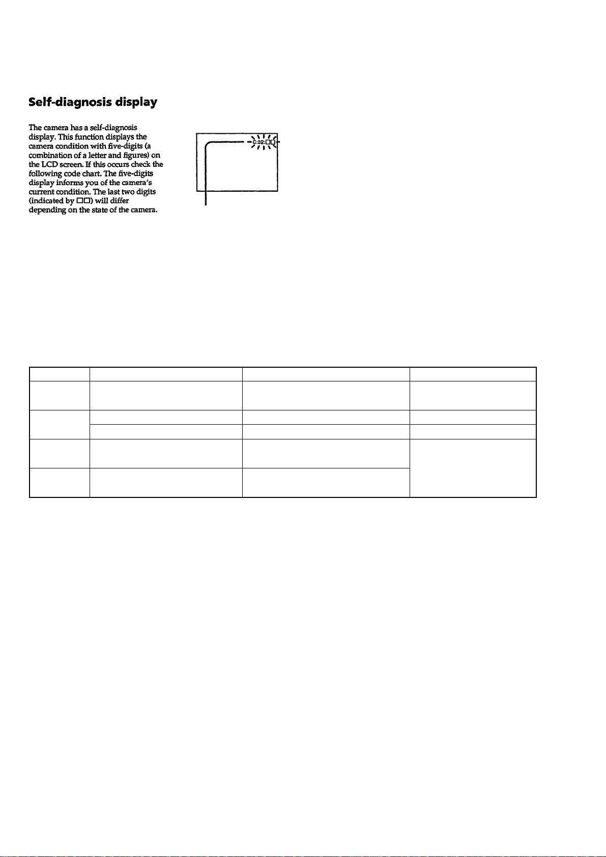
1-3. DESCRIPTION ON SELF-DIAGNOSIS DISPLAY
Self-diagnosis display
• C: ss: ss
You can reverse the camera
malfunction yourself. (However,
contact your Sony dealer or local
authorized Sony service facility
when you cannot recover from the
camera malfunction.)
• E: ss: ss
Contact your Sony dealer or local
authorized Sony service facility.
Display Code
C:32:ss
C:13:ss
E:61:ss
E:91:ss
Countermeasure
Turn the power off and on again.
Format the “Memory stick”.
Insert a new “Memory Stick”.
Checking of lens drive circuit.
Checking of flash unit or replacement
of flash unit.
Cause
Trouble with hardware.
Unformatted memory stick is inserted.
Memory stick is broken.
When failed in the focus initialization.
Abnormality when flash is being
charged.
Caution Display During Error
SYSTEM ERROR
FORMAT ERROR
MEMORY STICK ERROR
—
1-2E
Page 3

COVER
COVER
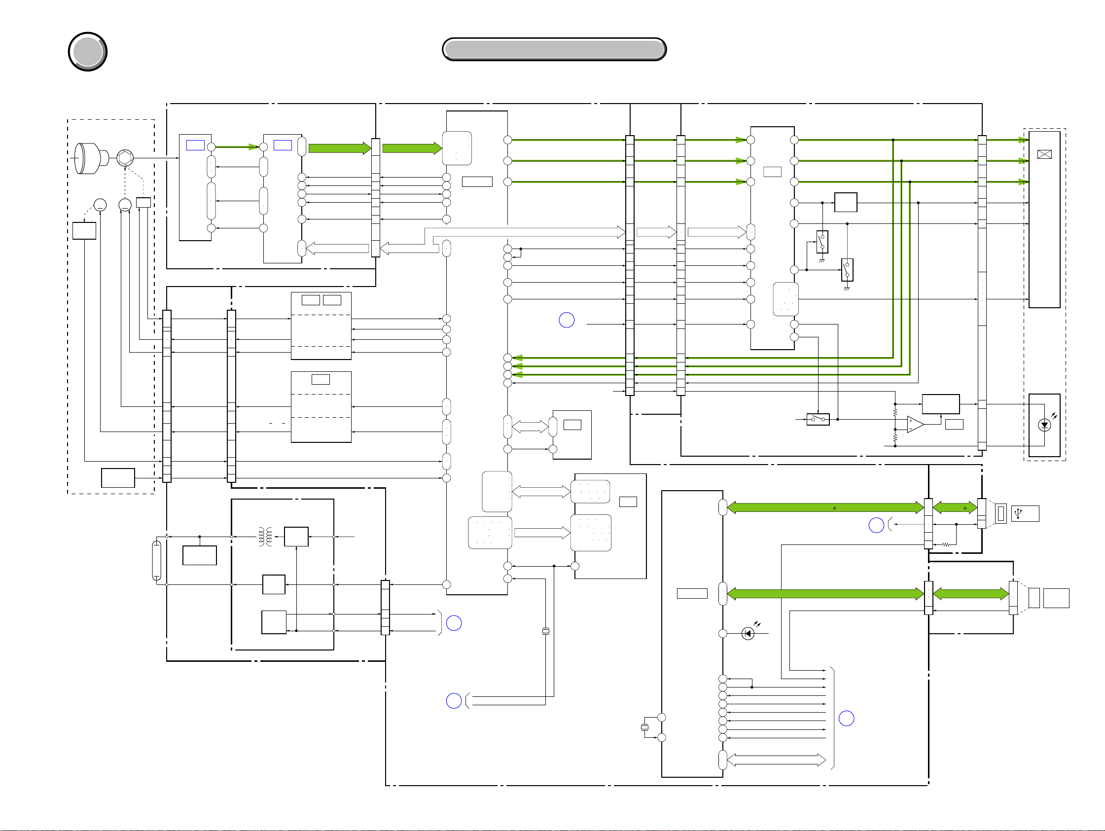
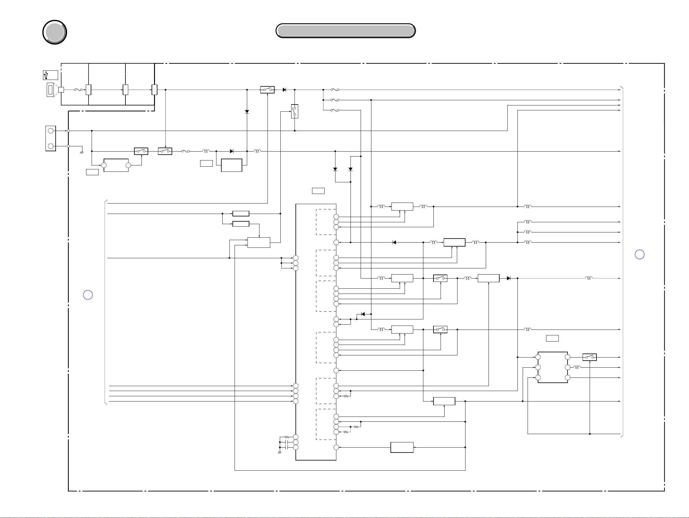
3. BLOCK DIAGRAMS
Link
Link
OVERALL BLOCK DIAGRAM (1/2) POWER BLOCK DIAGRAM (1/2)
OVERALL BLOCK DIAGRAM (1/2) POWER BLOCK DIAGRAM (1/2)
DSC-U30
OVERALL BLOCK DIAGRAM (2/2)
OVERALL BLOCK DIAGRAM (2/2)
POWER BLOCK DIAGRAM (2/2)
POWER BLOCK DIAGRAM (2/2)
Page 4
DSC-U30
COVER
COVER
SECTION 3
BLOCK DIAGRAMS
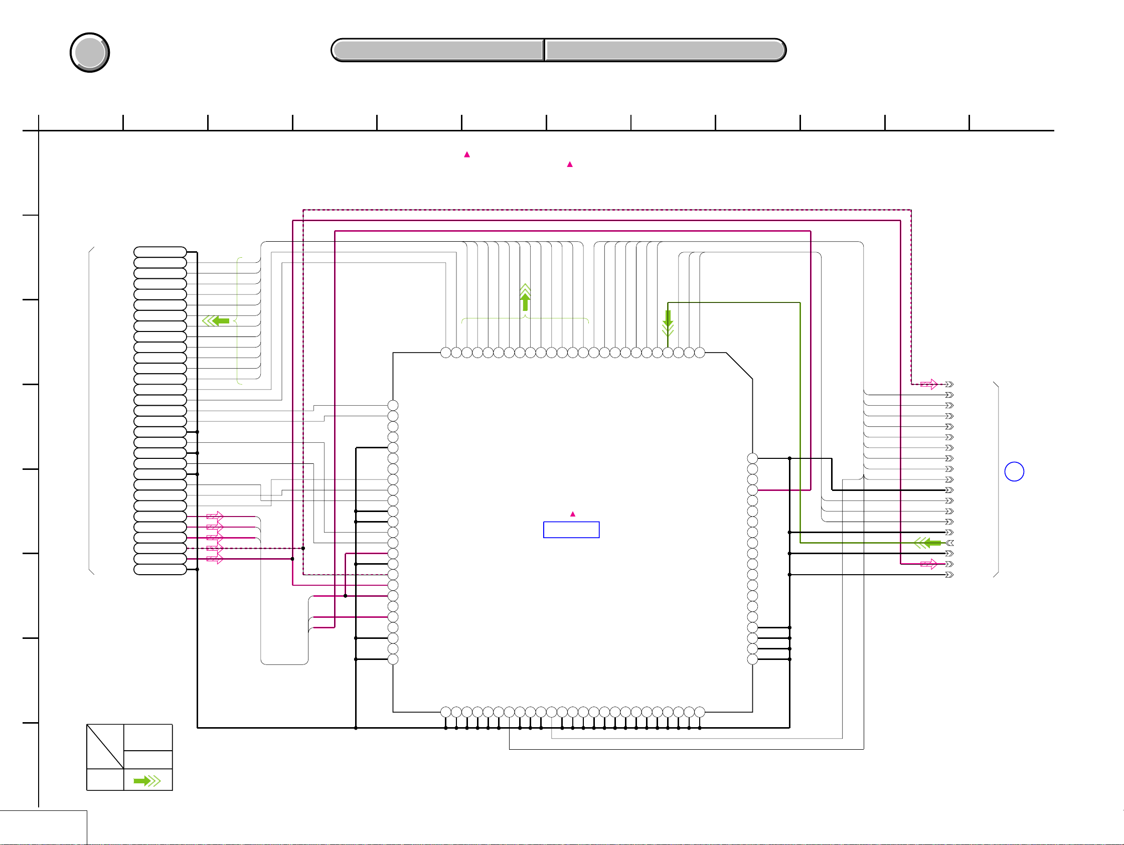
3-1. OVERALL BLOCK DIAGRAM (1/2)
CD-425 FLEXIBLE BOARD TY-20 BOARD (1/2)
10
12
RG, H1, H2
16
17
V1, V2A, V2B,
1
V2C, V3A, V3B,
ı
4
6
ı
9
18
CCD OUT
V3C, V4
VSHT
CN903
(1/2)
13
16
14
15
11
12
22
ı
25
17
21
IC101
4
CAMERA
1
MODULE
ı
(2/2)
3
5
ı
11
57
61
−
HALL+,
−
BIAS+,
−
DRIVE
+
DRIVE
FOCUS A, A, B, B
XFC RST SENS
LENS TEMP
H
IC302
CCD
IMAGER
(1/2)
SL-59 FLEXIBLE
BOARD
3
6
4
5
1
2
12
ı
15
7
11
ST-79 BOARD
CL601
CL531
ı
CL533
CL536,
537
T502
Q505 − 508
FLASH
DRIVE
Q504
FLASH
CHARGE
DETECT
XE A(H)
CHARGING
CAPACITOR
XE K (L)
05
ı
CL603
CL606,
607
LENS
FOCUS
MOTOR
FOCUS
SENSOR
LENS BLOCK
(SHUTTER)
IRIS
METER
M
LENS TEMP
SENSOR
IRIS
M
FLASH
UNIT
3. BLOCK DIAGRAMS
3. BLOCK DIAGRAMS
( ) : Number in parenthesis ( ) indicates the division number of schematic diagram where the component is located.
12
ı
CA AD00 − AD11
23
34
35
38
39
33
26
CAM SO, XCAM_SCK
27
IC202 IC206
(3/4)
HALL AMP,
HALL BIAS CONTROL,
HALL GAIN CONTROL
IRIS DRIVE
IC204
(3/4)
SHUTTER
DRIVE
FOCUS MOTOR
DRIVER
B+
SWITCH
CL501
CL507
CL526
CL516
CL508
Q501, 502
CA HD
CA FD
MCK
TG CLK
XCAM RESET
CL616
ı
CL622
CL641
CL631
CL623
CN902
19
ı
CA AD00 − AD11
30
8
9
13
11
7
15
CAM SO, XCAM_SCK
16
HALL AD
HALL GAIN
HALL OFFSET
IRIS CONT1
CAM DD ON, MSHUT ON
PE EN0, PE DIR0A, PE DIR0B
ı
ST UNREG
10
8
4
CA HD
CA FD
MCK
TG CLK
XCAM RESET
CN903 (2/2)
STRB ON
XSTB FULL
STB CHARGE
OVERALL (2/2)
(PAGE 3-4)
135 − 139
141 − 143
147 149
151 152
130
127
126
125
227
252
253
39
35
36
33
109
228
119
122
123
124
202
41
107
1
2
CAMERA DSP,
100
IC602 (1/2)
MAIN CPU
(1/4)
CAM SO, XCAM_SCK
167
218
242
243
245
261 − 263
265 − 267
270 − 275
277 − 279
281
18 19 50 51
53 − 55 57 − 59
61 − 63 65 − 67
70 71 73 74
213
OVERALL (2/2)
(PAGE 3-4)
XRST SYS
USB CLK EN
PANEL R
PANEL G
99
PANEL B
98
88
86
87
44
45
46
47
EEPROM TXD,
RXD, SCK
EEPROM RST
MC D00 − D15
27
48MHz
OVERALL (2/2)
(PAGE 3-4)
VR
VG
VB
VP
MC A01 − A20
X601
2
ı
4
6219
3
IC604
EEPROM
(2/4)
XRST SYS
D 1.5V
F3 F6 G3 − G7
H2 H3 H6 H7
J2 − J4 J6 J7
B2 B6 B7
C1 C2 C6 − C8
D1 − D3 D6 D7
E1 − E3 E6 E7
F1 F8
C4
CN904
XHD
XVD
TG CLK
XCS LCD
FP-533
FLEXIBLE
BOARD (1/2)
(1/2)
19
20
21
13
14
16
15
10
12
17 17
25
26
24
23
32 2
IC603
16M
FLASH ROM
(2/4)
X603
27MHz
163
162
PD-174 BOARD (1/2)
CN401
(1/2)
PANEL R
15
PANEL G
14
PANEL B
13
20
CAM SO, XCAM_SCK
21
XHD
18
XVD
19
TG CLK
24
XCS LCD
22
XRST SYS
VR
9
VG
8
VB
10
VP
11
FL+VO
IC602 (2/2)
CAMERA DSP,
MAIN CPU
(1/4)
22
23
255
258
259
257
134
90
26
30
31
166
214
247
50
23
51
19
45
48
67
47
78
20
D902
(MS ACCESS)
IC401
LCD
DRIVE
13
41 − 43
63 64
72 76 77
PANEL 2.8V
USB SUSPEND
VR
61
VG
7
VB
8
62
32
65
15
5
Q461
USB D
OVERALL (2/2)
(PAGE 3-4)
MS DIO, MS BS, MS SCLK
MS INT
USB JACK IN
SYS V
USB HOLD
USB VBUS
XMC NMI
XMC HELP
XCS MC
Q403 − 406
PSIG
DRIVE
Q402
5
Q401
FL−VO
4
USB JACK IN
OVERALL (2/2)
(PAGE 3-4)
CN402
RGT, HCK1, HCK2,
HST, WIDE, DWN,
EN, VCK, VST
Q462
BACKLIGHT
4
DRIVE
IC461
BACKLIGHT
CONTROL
1
3
US-7 FLEXIBLE
BOARD
CN907 CN050
5
USB D
6
USB 5V
2
3
1
SW-376 FLEXIBLE
CN906
BOARD (1/2)
(1/2)
15
18
MS DIO, MS BS, MS SCLK
20
MS INT
19 6
VCC
PANEL UNIT
R
7
G
8
B
6
PSIG
9
COM
26
5
10
11
15
16
22
ı
25
LED A
1
LED K
3
2
3
1
LCD901
COLOR
LCD
D901
BACKLIGHT
(USB)
(MS CONNECTOR)
2
4
8
MEMORY
STICK
249
ı
251
FR SI , FR SO, XFR SCK
3-1 3-2
A : VIDEO SIGNAL
Page 5
DSC-U30
COVER
COVER
3. BLOCK DIAGRAMS
3. BLOCK DIAGRAMS
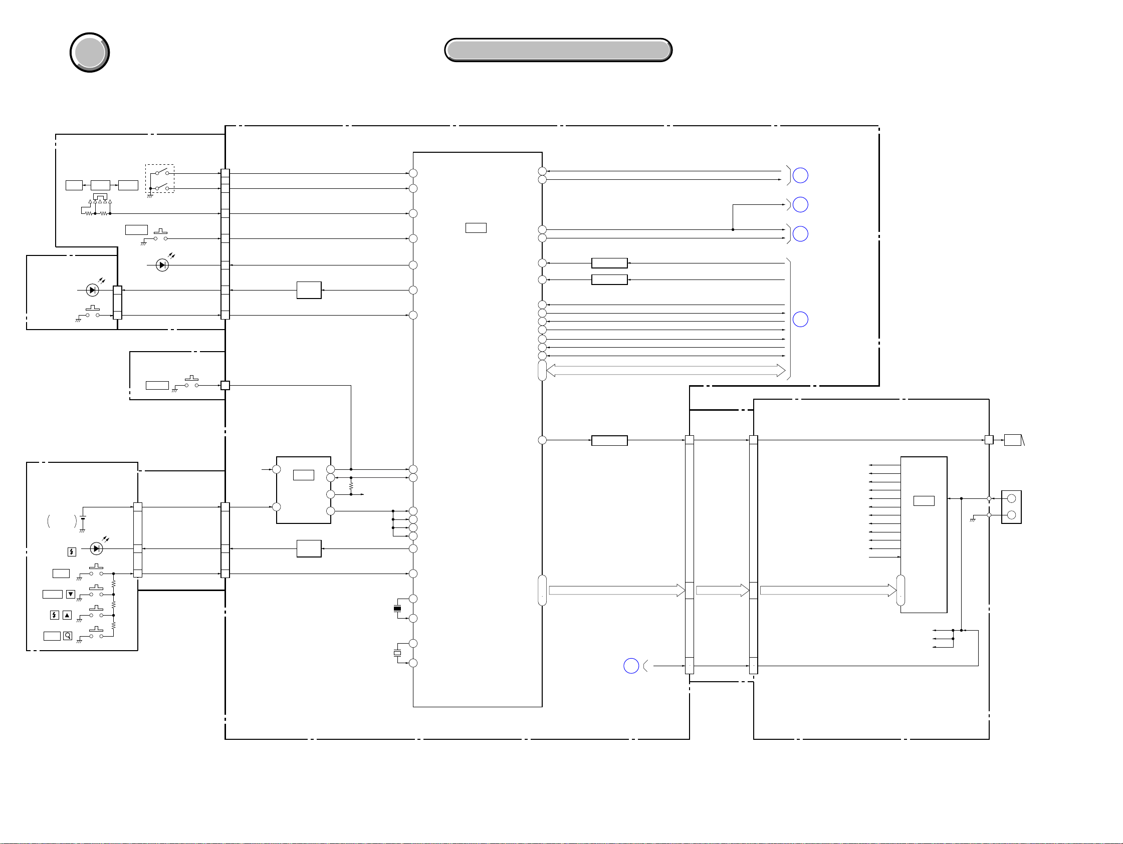
3-2. OVERALL BLOCK DIAGRAM (2/2)
SW-376 FLEXIBLE
BOARD (2/2)
S001
PLAY STILL MOVIE
OP-17 FLEXIBLE BOARD
D102
(SELF TIMER)
S101
(LENS COVER OPEN)
S003
(SHUTTER)
S002
POWER
D001
(POWER )
CN001
1
3
XSELF TIMER LED
XLENS CAP OPEN
RS-85 FLEXIBLE BOARD
METAL DISC
RESET
XSHUTTER
XAE LOCK SW
MODE DIAL
XPOWER ON
XPOWER LED
TY-20 BOARD (2/2)
CN906 (2/2)
11
10
12
9
6
3
5
CN908
XRESET SW ON
1
( ) : Number in parenthesis ( ) indicates the division number of schematic diagram where the component is located.
34
46
77
74
6
9
32
65
33
61
80
36
26
23
ı
25
Q401
INVERTER
Q403
INVERTER
FR SI, FR SO, XFR SCK
Q402 (1/2)
LED
DRIVE
4
5
54
IC401
1
17
19
3
HI CONTROL
(4/4)
XSTB FULL
STB CHARGE
XRST SYS
XRST SYS
USB CLK EN
MS INT
USB JACK IN
SYS V
USB HOLD
USB SUSPEND
USB VBUS
XMC NMI
XMC HELP
XCS MC
OVERALL (1/2)
1
(PAGE 3-1)
OVERALL (1/2)
3
(PAGE 3-1)
OVERALL (1/2)
2
(PAGE 3-1)
OVERALL (1/2)
5
(PAGE 3-2)
PD-174 BOARD (2/2)
BT480
LITHIUM
BATTERY
D481
S480
MENU
S481
SCENE
S482
S483
EXEC
FP-533 FLEXIBLE
CN401 (2/2)
BOARD (2/2)
28
27 7
29
VL 3V
XCHARGE LED
KEY AD0
EVER 4.0V
CN904 (2/2)
6
5
7
INITIAL RESET,
BACK UP VCC
3
IC402
(4/4)
Q402 (2/2)
LED
DRIVE
5
4
8
6
EVER 3.0V
BACKUP VCC
10MHz
X403
32.768kHz
X401
DD-209 BOARD
FP-532 FLEXIBLE
79
73
31
14
53
62
63
16
55
29
28
51
52
20
ı
UNREG SO, UNREG SCK, XCS DDCON, SYS DD ON
22
76
Q404, 405
MODULATOR
OVERALL (1/2)
(PAGE 3-2)
BUZZER
4
BOARD
50
41
ı
44
48
49
CN001CN901
BUZZER
2
EVER 4.0V
PANEL 2.8V
CAM 15V
PANEL 13.5V
BUZZER 15V
CAM −7.5V
EVER 3.0V
8
ı
UNREG SO, UNREG SCK, XCS DDCON, SYS DD ON
11
USB 5VUSB 5V
3
4
D 1.5V
D 2.8V
A 2.8V
M 5V
FL −VO
IC001
DC/DC
CONTROL
(2/2)
44
ı
46
57
BATT UNREG
ACV UNREG
ST UNREG
CN002
+
–
BZ901
BUZZER
BT901
BATTERY
TERMINAL
1
05
3-3 3-4
Page 6
COVER
COVER
3. BLOCK DIAGRAMS
3. BLOCK DIAGRAMS
DSC-U30
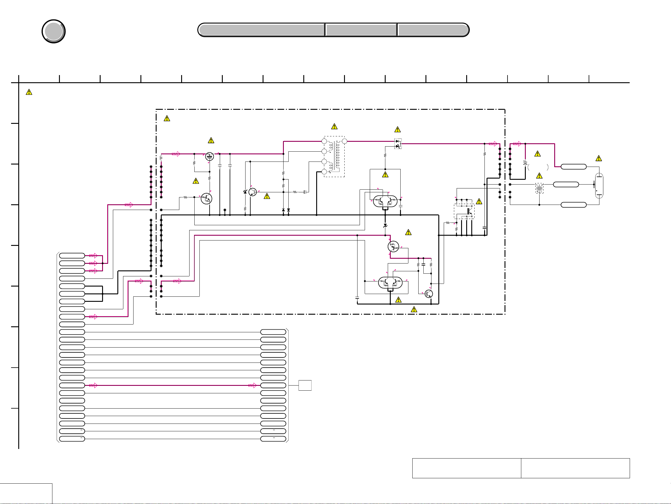
3-3. POWER BLOCK DIAGRAM (1/2)
DD-209 BOARD (1/2)
CN001 (1/2)
USB 5V
3
4
Q001, 004, 018
(USB)
BT901
BATTERY
TERMINAL
+
–
US-7
FLEXIBLE
BOARD
CN050
VCC
1
2
3
F005
BATT UNREG/+
BATT GND/–
IC002
VOLTAGE DETECT
(1/2)
TY-20 BOARD
(1/2)
CN901 (1/2)
CN907
USB 5V
USB UNREG SW
FAST CHARGE
Vout 1Vin2
49
48
FP-532
FLEXIBLE
BOARD
(1/2)
Q002, 006
( ) : Number in parenthesis ( ) indicates the division number of schematic diagram where the component is located.
F004
D001
L018 L019
IC004
(1/2)
D008
DC/DC
CONVERTER
SWITCH
SWITCH
Q007
Q011
Q010
EMERGENCY
DETECT
Q003, 005
D002
Q008, 009
IC001
DC/DC CONTROL
(2/2)
OUT1p
VCC2
F001
F002
F003
D009 D005
36
37OUT1n
55VIN1–
41
L001
Q013, 016
SWITCHING
D004
L008 L010
Q015, 017
L002 L009
SWITCHING
L012
L013
L014
ST UNREG
ACV UNREG
BATT UNREG
DD CON SENS
EVER 4.0V
D 1.5V
D 2.8V
A 2.8V
PANEL 2.8V
A
POWER (2/2)
(PAGE 3-7)
EVER 3.0V
UNREG SO
UNREG SCK
XCS DDCON
SYS DD ON
56
VCC1
47 RST
48 LDON
45
DATA
46
CLK
44 XCS
57 CONT
RT
7
CT1
6
8 CT2
OUT4p
SCPIN
30
31OUT4n
53VIN4–
39OUT5n
38OUT5p
43OUT5S
52VIN5–
D012
42VCC3
20VCC5
29OUT6n
28OUT6p
18OUT6s
50VIN6–
19VCC4
23OUT9
1SCP9
80IN9–
22OUT10
4AMPIN
5AMPOUT
3IN10–
10
L007
L005
Q020, 022
SWITCHING
Q021, 023
SWITCHING
Q012
EMERGENCY
DETECT
Q024
Q025
Q014
SWITCHING
L003
Q019
SWITCHING
D006, 007
L015
13.5V/15V/–7.5V REG
7
3
1
VCC
VEE
STB
IC003
(1/2)
REG2
REG1
REG3
L017
BUZZER 15V
M 5V
Q026, 027
6
L016
8
4
CAM 15V
PANEL 13.5V
CAM –7.5V
FL –VO
CAM DD ON
B
POWER (2/2)
(PAGE 3-7)
05
3-5 3-6
Page 7
DSC-U30
COVER
COVER
3. BLOCK DIAGRAMS
3. BLOCK DIAGRAMS
3-4. POWER BLOCK DIAGRAM (2/2)
TY-20 BOARD (2/2)DD-209 BOARD (2/2)
CN901 (2/2)
3
ST UNREG
ı
1
M 5V
17
16
CAM DD ON
15
BUZZER 15V
51
D 2.8V
19
18
CAM 15V
7
6
CAM –7.5V
9
8
A 2.8V A 2.8V
14
13
B
POWER (1/2)
(PAGE 3-6)
CN001 (2/2)
ST UNREG
M 5V
CAM DD ON
BUZZER 15V
D2.8V
CAM 15V
CAM –7.5V
A 2.8V
FP-532 FLEXIBLE
BOARD (2/2)
49
ı
51
35
36
37
1
33
34
45
46
43
44
38
39
( ) : Number in parenthesis ( ) indicates the division number of schematic diagram where the component is located.
SL-59 FLEXIBLE BOARD
BUZZER 15V
(MS ACCESS)
IC605
USB 1.5V REG
(2/4)
2
VIN
IC606
USB 3.1V REG
(2/4)
2
VIN
5
CE
D902
VOUT
VOUT
L202
FB202
D 2.8V
MS PWR ON
228
107
234
IC206
IRIS DRIVE,
HALL AMP
(3/4)
Q901
CAM DD ON
IC202
IRIS DRIVE,
HALL BIAS/GAIN
CONTROL
(3/4)
L201
D 2.8V
FB602
FB603
3
L604
L602
USB 1.5V
3
USB 3.1V
L601
L605
IC603
16M FLASH ROM
(2/4)
IC604
EEPROM
(2/4)
IC602
CAMERA DSP,
MAIN CPU
(1/4)
CAM DD ON
STRB ON
MS PWR ON
IC204
SHUTTER DRIVE,
FOCUS DRIVE
(3/4)
ST UNREG
STB CHARGE
XSTB FULL
Q201
F SENS VCC
L903
L902
L904
Q902
CAM –7.5V
FB902
D901
ST UNREG
CN903
1
ı
3
M 5V
9
STRB ON STRB ON
CN902
CAM 15V
FE3V
DRV3V
TG3V
CL636, 637 CL521, 522
10
4
8
18
CD-425 FLEXIBLE BOARD
2
3
4
5
6
CL501
CL616
ı
CL507
CL622
CL641 CL526
CL623 CL508
CL631 CL516
SW-376 FLEXIBLE BOARD OP-17 FLEXIBLE BOARD
CN906 CN001
D 2.8V
4
D 2.8V
7
MS VCC
21
22
ST-79 BOARD
L501
ı
M 5V
IC101
CAMERA
MODULE
(2/2)
D 2.8V
D001
(POWER)
VCC
Q501, 502
2
(MS CONNECTOR)
9
Q505 - 507
FLASH
DRIVE
L301
FB301
Q503
TRANS
DRIVE
MEMORY
STICK
STB CHARGE
XSTB FULL
IC302
CCD IMAGER
(1/2)
D102
(SELF TIMER)
2
1
3
4
T502
PS
F
C601
CHARGING
D502
5
Q508
Q504
CL531
CL533
CL536, 537
F SENS VCC
CAPACITOR
XE A(H)
CL601
ı
ı
CL603
+
XE K(L)
CL606, 607
LENS BLOCK
8
FOCUS
SENSOR
FLASH
UNIT
POWER (1/2)
(PAGE 3-5)
05
40
D 1.5V
ı
42
FL –VO
EVER 4.0V
EVER 3.0V
28
29
30
31
32
13
14
15
16
17
10
9
11
8
6
7
12
PANEL 13.5V
PANEL 2.8V
DD CON SENS
BATT UNREG
ACV UNREG
UNREG SO
UNREG SCK
XCS DDCON
SYS DD ON
A
FAST CHARGE
USB UNREG SW
12
D 1.5V
ı
10
FL –VO
24
PANEL 13.5V
23
22
PANEL 2.8V
21
20
EVER 4.0V
39
38
DD CON SENS
37
BATT UNREG
36
ACV UNREG
35
UNREG SO
42
UNREG SCK
43
XCS DDCON
41
SYS DD ON
44
FAST CHARGE
46
USB UNREG SW
45
EVER 3.0V
40
66 DD CON SENS
BATT SENS
67
68 ACV SENS
20 UNREG SO
21 UNREG SCK
22 XCS DDCON
76 SYS DD ON
48
72 USB UNREG SW
USB PWR ON
FAST CHARGE
STB CHG
XSTB FULL
IC401
HI CONTROL
(4/4)
78
STB CHARGE
46
34
BackUp Vcc
XSTB FULL
D 1.5V
EVER 4.0V
3.3V REG
2
VIN
4
CE
INITIAL RESET, BACK UP VCC
L401
6
VOUT
8
VRO
IC403
(4/4)
IC402
(4/4)
VOUT
VIN
VBAT
FP-533 FLEXIBLE
BOARD
CN904
32
33
3
D402
7
3
30
29
28
27
6
D 2.8V
FL +VO
FL –VO
PANEL 13.5V
PANEL 2.8V
VL 3V
268
28
2
1
4
5
6
7
CN401
L401
LITHIUM
BATTERY
BT480
D481
IC461
BACKLIGHT
CONTROL
POFF E3
IC401
LCD DRIVER
4
Q408, 409
59
Q462
BACKLIGHT
DRIVE
Q410
REF VOLTAGE
GEN.
D402
CN402
LED A
1
LED K
3
CRext
12
REF
14
VDDG
19
VDD
21
PANEL UNIT
D901
BACKLIGHT
LCD901
COLOR
LCD
PD-174 BOARD
3-7 3-8 E
Page 8
COVER
COVER
PRINTED WIRING BOARDS AND SCHEMATIC DIAGRAMS
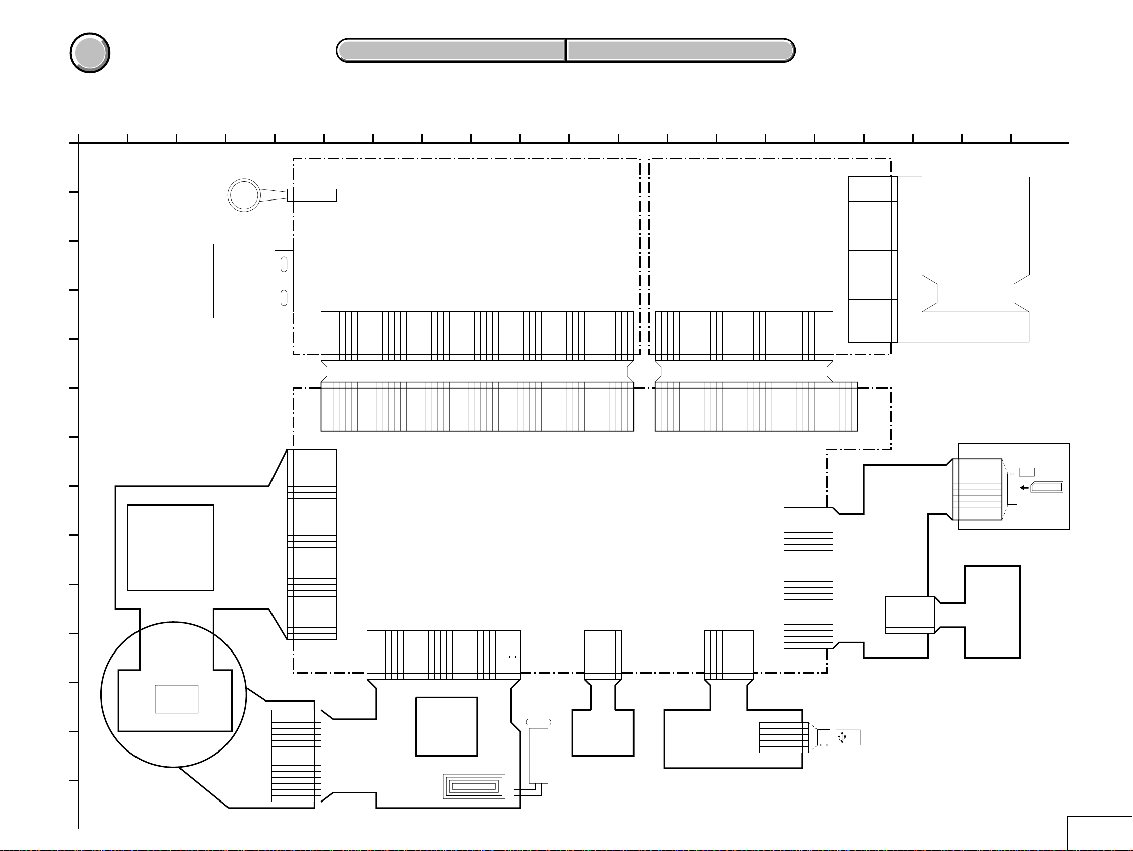
4-1. FRAME SCHEMATIC DIAGRAM
SECTION 4
4-2. SCHEMATIC DIAGRAMS 4-3. PRINTED WIRING BOARDS
4-2. SCHEMATIC DIAGRAMS 4-3. PRINTED WIRING BOARDS
DSC-U30
FRAME SCHEMATIC DIAGRAM
A
B
C
D
E
F
BZ901
BUZZER
BATTERY
TERMINAL
BT901
5
CN002
1 BUZZER
2 GND
76
2P
81410
DD-209 BOARD PD-174 BOARD
51P
CN001
BUZZER_15V2BUZZER3USB_5V4USB_5V5REG_GND6FAST_CHARGE7USB_UNREG_SW8SYS_DD_ON9UNREG_SCK10UNREG_SO11XCS_DDCON12EVER_3.0V13EVER_4.0V14EVER_4.0V15DD_CON_SENS16BATT_UNREG17ACV_UNREG18REG_GND19REG_GND20REG_GND21REG_GND22REG_GND23REG_GND24REG_GND25REG_GND26REG_GND27REG_GND28FL_-VO29PANEL_13.5V30PANEL_13.5V31PANEL_2.8V32PANEL_2.8V33D_2.8V34D_2.8V35M_5V36M_5V37CAM_DD_ON38A_2.8V39A_2.8V40D_1.5V41D_1.5V42D_1.5V43CAM_-7.5V44CAM_-7.5V45CAM_15V46CAM_15V47REG_GND48REG_GND49ST_UNREG50ST_UNREG51ST_UNREG
1
FP-532 FLEXIBLE BOARD FP-533 FLEXIBLE BOARD
4
6
8
10
13
15
16
18
20
21
22
23
24
25
M_5V17M_5V
A_2.8V14A_2.8V
PANEL_2.8V
PANEL_13.5V
PANEL_2.8V
D_2.8V19D_2.8V
CAM_DD_ON
FL_-VO
REG_GND26REG_GND27REG_GND28REG_GND29REG_GND30REG_GND31REG_GND32REG_GND33REG_GND34REG_GND
PANEL_13.5V
D_1.5V11D_1.5V12D_1.5V
CAM_15V7CAM_15V
REG_GND5REG_GND
CAM_-7.5V9CAM_-7.5V
51P
CN901
50
51
BUZZER
BUZZER_15V
35
36
37
38
40
41
42
43
44
45
46
47
48
USB_5V49USB_5V
REG_GND
FAST_CHARGE
USB_UNREG_SW
UNREG_SCK
SYS_DD_ON
UNREG_SO
XCS_DDCON
EVER_3.0V
EVER_4.0V39EVER_4.0V
BATT_UNREG
DD_CON_SENS
ACV_UNREG
12
29P
CN401
1
33P
ST_UNREG2ST_UNREG3ST_UNREG
CN904
139
FL_-VO2FL_+VO3REG_GND4PANEL_13.5V5PANEL_13.5V6PANEL_2.8V7PANEL_2.8V8VG9VR10VB11VP12REG_GND13PANEL_B14PANEL_G15PANEL_R16REG_GND17XRST_SYS18XHD19XVD20LCD_SO21XLCD_SCK22XCS_LCD23REG_GND24TG_CLK25REG_GND26D_2.8V27XCHARGE_LED28VL_3V29KEY_AD0
1
14
15
16
17
18
19
21
22
PANEL_2.8V
23VP24VB25VR26VG27
XVD
XHD
REG_GND
PANEL_B
LCD_SO
PANEL_R20PANEL_G
REG_GND
XRST_SYS
33
FL_-VO
32
FL_+VO
31
REG_GND
29
30
PANEL_13.5V
PANEL_13.5V
28
PANEL_2.8V
13
XLCD_SCK
12
XCS_LCD
11
REG_GND
10
TG_CLK
9
REG_GND
8
D_2.8V
6
7
VL_3V
XCHARGE_LED
16
4
5
KEY_AD0
MODE_DIAL (N.C.)
1
2
3
XPOWER_ON (N.C.)
XPOWER_LED (N.C.)
XRESET_SW_ON (N.C.)
LED_A
LED_K
174
27PCN402
1
N.C.
2
3
TEST2
4
RGT
5
B
6
R
7
G
8
PSIG
9
HCK1
10
HCK2
11
CRext
12
DSUT
13
REF
14
HST
15
WIDE
16
CS
17
VSSG
18
VDDG
19
VSS
20
VDD
21
DWN
22
EN
23
VCK
24
VST
25
COM
26
TEST
27
183 15 19 201 112
PANEL UNIT
LCD901
1inch
COLOR LCD
D901
LED BACKLIGHT
31PCN902
CD_GND
1
CAM_15V
G
H
IC101
CAMERA MODULE
I
(CH-124 BOARD) BOARD
CD-425
FLEXIBLE
J
K
L
M
CCD
LENS
N
2
CAM_-7.5V
3
FE3V
4
DRV3V
5
TG3V
6
XCAM_RESET
7
CA_HD
8
CA_FD
9
CD_GND
10
TG_CLK
11
CD_GND
12
MCK
13
CD_GND
14
XCAM_SCK
15
CAM_SO
16
XCAM_CS
17
XTG_CS
18
CA_AD0
19
CA_AD4
20
CA_AD8
21
CA_AD1
22
CA_AD5
23
CA_AD9
24
CA_AD2
25
CA_AD6
26
CA_AD10
27
CA_AD3
28
CA_AD7
29
CA_AD11
30
CD_GND
31
XFC_RST_SENS
F_SENS_VCC
F_SENS_GND
LENS TEMP
FOCUS_B
FOCUS_A
FOCUS_B
FOCUS_A
DRIVE-
DRIVE+
HALL-
BIAS+
HALL+
23PCN906
XAE_LOCK_LED (N.C.)
XTALLY_LED (N.C.)
XSELF_TIMER_LED
CN050
XLENS_CAP_OPEN
5P
TY-20 BOARD
25PCN903
ST_UNREG2ST_UNREG3ST_UNREG4STB_CHARGE5REG_GND6REG_GND7REG_GND8XSTB_FULL9M_5V10STRB_ON11DRIVE-12DRIVE+13HALL-14BIAS+15BIAS-16HALL+17XFC_RST_SENS18F_SENS_VCC19F_SENS_GND20N.C.21LENS_TEMP22FOCUS_B23FOCUS_A
1
15P
1
2
3
4
BIAS-
5
6
7
SL-59
8
FLEXIBLE
9
N.C.
10
BOARD
11
12
13
14
15
ST-79
BOARD
FLASH UNIT
FOCUS_B25FOCUS_A
24
C601
CHARGING
CAPACITOR
6PCN908
XRESET_SW_ON2REG_GND3XCPC_IN (N.C.)4EVER_4.0V (N.C.)5LANC_IN (N.C.)6LANC_OUT (N.C.)
1
RS-85
FLEXIBLE
BOARD
8PCN907
USB_JACK_IN2USB_5V3USB_5V4REG_GND (N.C.)5USB_D+6USB_D-7USB_GND8USB_GND
1
US-7
FLEXIBLE BOARD
XPOWER_LED
XPOWER_ON
XAE_LOCK_SW
XSHUTTER
MODE_DIAL
MS_VSS
MS_VCC (N.C.)
MS_VCC (N.C.)
MS_DIO
MS_INT
MS_SCLK
MS_VCC
MS_VCC
MS_VSS
1VCC
2D-
3D+
4ID
5GND
D_2.8V
D_2.8V
MS_BS
1
2
3
4
5
6
7
GND
8
9
10
11
12
GND
13
14
15
16
17
18
19
20
21
22
23
SW-376
FLEXIBLE
(USB)
BOARD
CN001
XSELF_TIMER_LED
XLENS_CAP_OPEN
STATIC_GND
D_2.8V
6P
1
2
3
GND
4
5
N.C.
6
MS CONNECTOR
10P
VSS
1
BS
2
VCC (N.C.)
3
DIO4
5
N.C
6
INT
7
N.C
SCLK
8
VCC
9
VSS
10
OP-17
FLEXIBLE
BOARD
10
MEMORY
STICK
MEMORY STICK
1
05
4-1 4-2
FRAME
Page 9
COVER
COVER
4-2. SCHEMATIC DIAGRAMS
Link
Link
CD-425 FLEXIBLE BOARD (1/2)
CD-425 FLEXIBLE BOARD (1/2)
(CCD IMAGER)
(CCD IMAGER)
US-7 FLEXIBLE BOARD
US-7 FLEXIBLE BOARD
DSC-U30
(USB CONNECTOR)
(USB CONNECTOR)
CD-425 FLEXIBLE BOARD (2/2)
CD-425 FLEXIBLE BOARD (2/2)
(CAMERA MODULE)
(CAMERA MODULE)
SL-59 FLEXIBLE BOARD
SL-59 FLEXIBLE BOARD
(CHARGING CAPACITOR, FLASH UNIT)
(CHARGING CAPACITOR, FLASH UNIT)
ST-79 BOARD
ST-79 BOARD
COMMON NOTE FOR SCHEMATIC DIAGRAMS WAVEFORMS
COMMON NOTE FOR SCHEMATIC DIAGRAMS WAVEFORMS
(FLASH DRIVE)
(FLASH DRIVE)
OP-17 FLEXIBLE BOARD
OP-17 FLEXIBLE BOARD
(LENS COVER DETECT)
(LENS COVER DETECT)
SW-376 FLEXIBLE BOARD
SW-376 FLEXIBLE BOARD
(CONTROL SWITCH, MS CONNECTOR)
(CONTROL SWITCH, MS CONNECTOR)
RS-85, FP-532, FP-533 FLEXIBLE BOARD
RS-85, FP-532, FP-533 FLEXIBLE BOARD
Page 10

COVER
COVER
For Schematic Diagram
• Refer to page 4-37 for printed wiring board.
• Refer to page 4-57 for waveform.
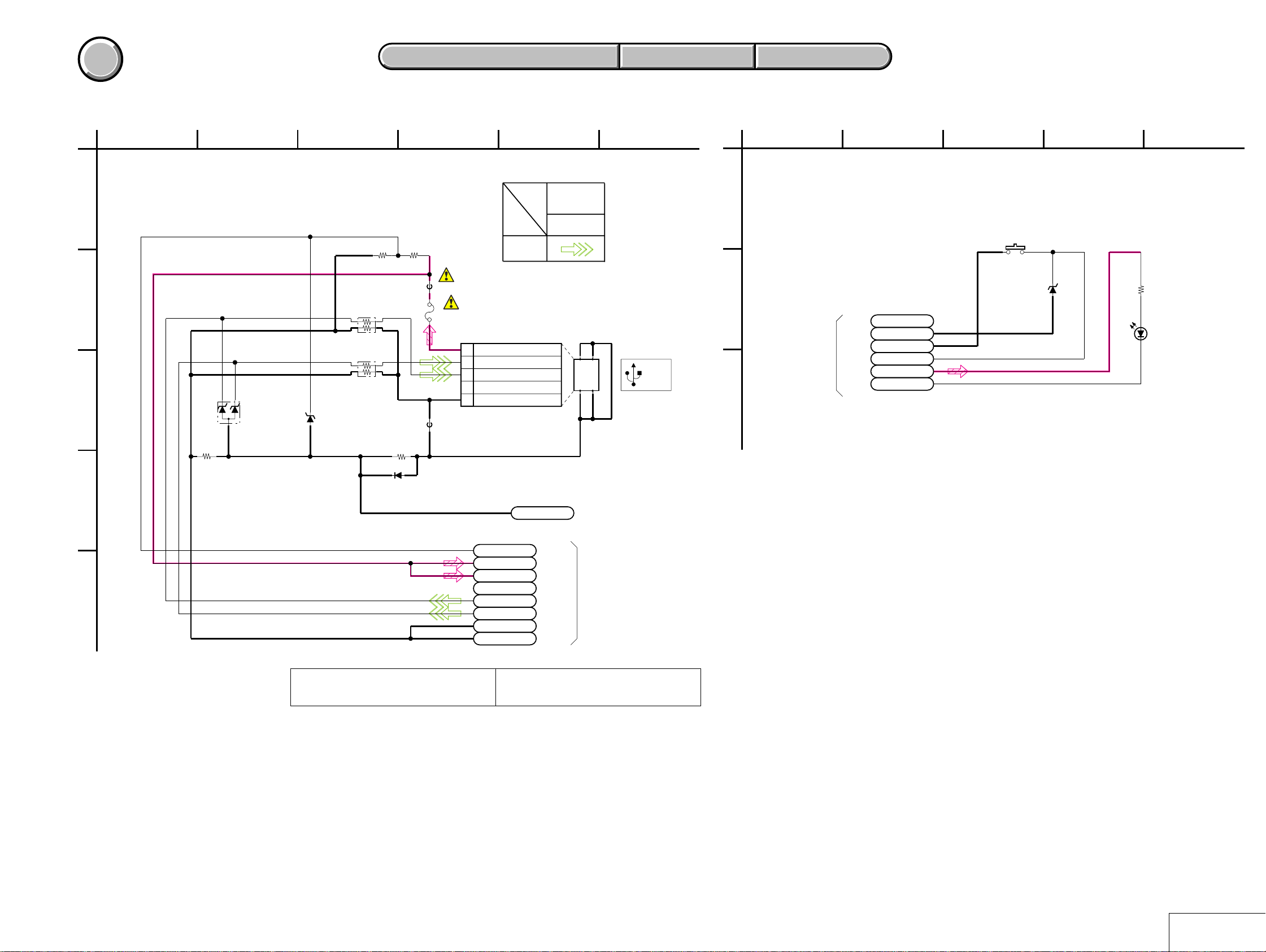
4-2. SCHEMATIC DIAGRAMS CD-425 FLEXIBLE BOARD
4-2. SCHEMATIC DIAGRAMS CD-425 FLEXIBLE BOARD
DSC-U30
1
32
4
56
7
8
9
CD-425 FLEXIBLE BOARD (1/2)
A
B
C
D
CCD IMAGER(CCD1 BLOCK)
XX MARK:NO MOUNT
NO MARK:REC/PB MODE
R:REC MODE
P:PB MODE
1
(2/2)
V3B
CAM_-7.5V
V3C
V2C
V3A
V2B
V2AV4V1
VSHT
GND
H1RGH2
GND
CCD_OUT
GND
CAM_15V
GND
L301
100uH
1
3
1
6
Q302
2SC4250(T5LSONY1)
BUFFER
R311
R11.8/P0
C311
0
XX
CH
R308
5.6k
R15.1/P0
R11.1/P0
C312
CH
C309
0.1u
16V
XX
V42V3A
Note:The voltage and
waveform of IC302
cannot be measured,
because it is mounted
by the side of lens.
V3B4V3C5VHOLD
E
D301
MA111-(K8).S0
R303
0
R304
0
0
C314
R302
C305
0.22u
R301
C313
100k
0.01u
10u
F
C301
0.22u
25V
FB301
HS601
C302
C315
1.5u
G
SIGNAL PATH
VIDEO
SIGNAL
1.5u
35V
35V
C303
10u
Y/CHROMA
REC
25V
R306
φ SUB
18
0
C307
2200p
IC302
CCD IMAGER
IC302
ICX454JQF-13
GND15VL16H117H2
14
V2A7V2B8V2C9V1
VDD
GND
10
11
12RG13
C306
0.1u
16V
R307
3.9k
VOUT
C310
0.1u
16V
Precautions for Replacement of CCD Imager
•The CD-425 flexible board mounted as a repair part is not
equipped with a CCD imager.
When replacing this board, remove the CCD imager from the
old one and mount it onto the new one.
• If the CCD imager has been replaced, carry out all the
adjustments for the camera section.
• As the CCD imager may be damaged by static electricity from
H
its structure, handle it carefully like for the MOS IC.
In addition, ensure that the receiver is not covered with dusts
nor exposed to strong light.
05
4-7 4-8
CD-425 (1/2)
Page 11
DSC-U30
COVER
COVER
For Schematic Diagram
• Refer to page 4-37 for printed wiring board.
4-2. SCHEMATIC DIAGRAMS CD-425 FLEXIBLE BOARD
4-2. SCHEMATIC DIAGRAMS CD-425 FLEXIBLE BOARD
1
2
5 12
89674
10
113
:Voltage measurment of the CSP ICs
CD-425 FLEXIBLE BOARD(2/2)
A
B
C
D
E
F
CAMERA MODULE(CH BLOCK)
TY-20
(2/4)
CN902
(PAGE 4-14)
LND101
31
LND102
LND103
LND104
LND105
LND106
LND107
LND108
LND109
LND110
LND111
LND112
LND113
LND114
LND115
LND116
LND117
LND118
LND119
LNC120
LND121
LND122
LND123
LND124
LND125
LND126
LND127
LND128
LND129
LND130
1
LND131
CD_GND
CA_AD11
CA_AD7
CA_AD3
CA_AD10
CA_AD6
CA_AD2
CA_AD9
CA_AD5
CA_AD1
CA_AD8
CA_AD4
CA_AD0
XTG_CS
XCAM_CS
CAM_SO
XCAM_SCK
CD_GND
MCK
CD_GND
TG_CLK
CD_GND
CA_FD
CA_HD
XCAM_RESET
TG3V
DRV3V
FE3V
CAM_-7.5V
CAM_15V
CD_GND
TG3V
DRV3V
FE3V
D11
D10
D7
D3
D6
D2
D9
D5
D1
D8
D4
D0
XCAM_SO
26
XCAM_SCK
27
D1
28
D0
29
GND
30
CLPOB
31
CLPDM
32
XCAM_RESET
33
CA_HD
34
CA_FD
35
GND
36
GND
37
MCK
38
TG_CLK
39
HVDD
40
GND
41
CAM_-7.5V
42
CAM_15V
TG3V
FE3V
DRV3V
43
TG3V
44
WEN
45
FE3V
46
DRV3V
47
GND
48
GND
49
GND
50
and the Transistors with mark,are
not possible.
D6
D7
D8
D9
D10
D11
24
25
D1021D1122D1223D13
XTG_CS
XGCAM_CS
D5
D3
D4
IC101
CAMERA MODULE
(CH-124 BOARD)
D0
D1
D2
IC101
V3C
V3B
V3A
V2A
10V411
12D213D314D415D516D617D718D819D920
VSHT
V2BV4V2C
5
7V28
V3A9V3B
V1A6V1B
RG
3RG4
CCD_OUT
H2
H1
CCD_OUT
1
H12H2
CAM_-7.5V
V3C
V2C
V4
V3A
V3B
V1
V2A
V2B
VSHT
GND
RG
H1
H2
GND
CCD_OUT
GND
CAM_15V
GND
1
(1/2)
DRV3V
(XCAM_SO)
(D13)
GND
GND
(D1)
(D5)
(D9)
GND
GND
GND
GND
V3C
V2C
V4
V3A
V3B
V1
95
93 94
RG
H1
H2
85 86 87 88 89 90 91 92
84
83
82
81
80
79
78
77
76
V2A
V2B
VSHT
G
H
05
CD-425 (2/2)
SIGNAL PATH
REC
VIDEO
SIGNAL
Y/CHROMA
GND52GND53GND54GND55GND56GND57V158GND59GND60GND61SUB62GND63GND64GND65GND66GND67GND68GND69GND70GND71GND72GND73GND74GND75GND
51
VSHT
V1
4-9 4-10
Page 12

Schematic diagrams of the TY-20, PD-174 and DD-209 boards are not shown.
Pages from 4-11 to 4-24 are not shown.
Page 13
DSC-U30
COVER
COVER
For Schematic Diagram
• Refer to page 4-45 for printed wiring board. (SL-59 FLEXIBLE BOARD)
• Refer to page 4-47 for printed wiring board. (ST-79 BOARD)
3 151 112
SL-59 FLEXIBLE BOARD
A
CHARGING CAPACITOR,FLASH UNIT
4
(Including ST-79 board)
B
CL622
CL621
CL620
C
D
LND601
ST_UNREG
1
E
F
TY-20 (3/4)
CN903
G
(PAGE4-15)
H
I
05
25
LND602
ST-UNREG
LND603
ST_UNREG
LND604
STB_CHARGE
LND605
REG_GND
LND606
REG_GND
LND607
REG_GND
LND608
XSTB_FULL
LND609
M_5V
LND610
STRB_ON
LND611
DRIVE- DRIVE-
LND612
DRIVE+
LND613
HALL-
LND614
BIAS+
LND615
BIAS-
LND616
HALL+
LND617
XFC_RST_SENS
LND618
LND619
F_SENS_GND F_SENS_GND
LND620
NC
LND621
LENS_TEMP
LND622
FOCUS_B
LND623
FOCUS_A
LND624
FOCUS_B
LND625
FOCUS_A
CL619
CL618
CL617
CL616
CL623
CL658
CL657
CL656
CL655
CL654
CL630
CL629
CL628
CL627
CL626
CL631
CL637
CL636
CL641
4-2. SCHEMATIC DIAGRAMS
4-2. SCHEMATIC DIAGRAMS
5
ST-79 BOARD
FLASH DRIVE(ST BLOCK)
XX MARK:NO MOUNT
Q502
MCH3306-TL
B+ SWITCH
L501
10uH
CL507
CL506
CL501
CL502
CL503
CL505
CL504
CL508
CL554
CL556
CL555
CL558
CL557
CL514
CL513
CL512
CL511
CL516
CL521
CL522
CL526
R501
4700
R502
100k
Q501
DTC144EHT2L
SWITCHING
0
2.4
R503
10k
0.3
2.4
C503
2.4
CL559
SL-59 FLEXIBLE BOARD ST-79 BOARD
SL-59 FLEXIBLE BOARD ST-79 BOARD
76
81410
12
139
NO MARK:REC/PB MODE
R:REC MODE
P:PB MODE
C504
10u
10u
0.3
D505
XX
CPH3205-SONY-TL-E
R514
0
0.3
Q503
TRANS DRIVE
LND629
LND630
DRIVE+
LND631
HALLLND632
BIAS+
LND633
BIASLND634
HALL+
LND635
XFC_RST_SENS
LND636
F_SENS_VCCF_SENS_VCC
LND637
LND638
NC
LND639
LENS_TEMP
LND640
FOCUS_B
LND641
FOCUS_A
LND642
FOCUS_B
LND643
FOCUS_A
R513
2200
R505
0
D501
MA111-(K8).S0
R506
470
C506
0.22u
D504
XX
1
LENS
BLOCK
LENS BLOCK is replaced as a block.
So that there PRINTED WIRING BOARD and
SCHEMATIC DIAGRAM are omitted.
15
T502
CHARGE TRANS
PFS
2
1
3
4
D502
RN1902FE(TPL3)
FLASH CHARGE
0
2
D503
XX
R5/P0
0
2
Q504
DETECT
6
1
R5/P0
HAU160C030TP
R507
4700
2.8
3
4
0
6
1
5
0
3
4
0
C508
1u
Q506
DTA114EHT2L
B+ SWITCH
R5/P0
R508
0
5
Q505
RN1902FE(TPL3)
SWITCHING
C509
0.047u
1k
0
2SD2216J-QR(K8).SO
FLASH DRIVE
R509
0
Q507
CL531
R512
CL532
4.7M
CL533
CL552
CL551
CL553
CL541
Q508
CY25AAJ-8-T13
208
FLASH SWITCH
8
7
65
IGBT
R510
47
4
1
23
0
R511
1M
150
C511
47000pF
250V
CL537
CL536
CL603
CL602
CL601
CL653
CL652
CL651
CL611
CL606
CL607
C601
42u
330V
CHARGING
CAPACITOR
L601
LND626
TRIGGER
LND627
XE_A(H)
LND628
XE_K(L)
FLASH UNIT
5
0
C507
0.1u
SL-59, ST-79
The components identified by mark 0 or dotted
line with mark 0 are critical for safety.
Replace only with part number specified.
4-25 4-26
Les composants identifiés par une marque 0 sont
critiques pour la sécurité. Ne les remplacer que
par une piéce portant le numéro spécifié.
Page 14
DSC-U30
COVER
COVER
For Schematic Diagram
• Refer to page 4-49 for printed wiring board.
US-7 FLEXIBLE BOARD
A
B
C
USB CONNECTOR
XX MARK:NO MOUNT
R051
XX
MAZT082H08S0
D050
312
RB001
RB002
D051
MA8082-(K8).S0
4-2. SCHEMATIC DIAGRAMS
4-2. SCHEMATIC DIAGRAMS
US-7 FLEXIBLE BOARD OP-17 FLEXIBLE BOARD
US-7 FLEXIBLE BOARD OP-17 FLEXIBLE BOARD
For Schematic Diagram
• Refer to page 4-51 for printed wiring board.
4
5
SIGNAL PATH
VIDEO
SIGNAL
6
OP-17 FLEXIBLE BOARD
A
LENS COVER DETECT
Y/CHROMA
R053
R052
330k
100k
FB050
PB
B
0
0
FB051
XX
R054
0
USB
USB
F005
(0.5A/50V)
VCC
1
D-
2
D+
3
4ID
5
GND
6
5PCN050
(USB)
SW-376
FLEXIBLE
CN001
(PAGE 4-29)
1
LND102
LND103
LND104
LND105
LND106
STATIC_GND
GND
XLENS_CAP_OPEN
D_2.8V
XSELF_TIMER_LED
N.C.
LND101
C
05
312
S101
(LENS COVER OPEN)
1
D101
MAZS051008SO
2
4
R101
680
5
D102
SML-310LTT86
(SELF TIMER)
D
E
D052
XX
LND058
STATIC GND
USB_JACK_IN
USB_5V
USB_5V
REG_GND (N.C.)
USB
USB_D+
USB_D-
USB
USB_GND
05
The components identified by mark 0 or dotted
line with mark 0 are critical for safety.
Replace only with part number specified.
USB_GND
Les composants identifiés par une marque 0 sont
critiques pour la sécurité. Ne les remplacer que
par une piéce portant le numéro spécifié.
LND050
LND051
LND052
LND053
LND054
LND055
LND056
LND057
1
TY-20 (4/4)
(PAGE 4-18)
8
CN907
4-27
4-28
US-7, OP-17
Page 15

DSC-U30
COVER
COVER
For Schematic Diagram
• Refer to page 4-53 for printed wiring board.
4-2. SCHEMATIC DIAGRAMS SW-376 FLEXIBLE BOARD
4-2. SCHEMATIC DIAGRAMS SW-376 FLEXIBLE BOARD
A
B
C
D
E
F
312
SW-376 FLEXIBLE BOARD
CONTROL SWITCH,MS CONNECTOR
CN001
6P
1XSELF_TIMER_LED
OP-17
FLEXIBLE
LND101-106
(PAGE 4-28)
TY-20 (4/4)
CN906
(PAGE 4-18)
1
23
LND022
LND021
LND020
LND019
LND018
LND017
LND016
LND015
LND014
LND013
LND012
LND011
LND010
LND009
LND008
LND007
LND006
LND005
LND004
LND003
LND002
LND001
XTALLY_LED (N.C.)
XSELF_TIMER_LED
D_2.8V
XLENS_CAP_OPEN
XPOWER_LED
D_2.8V
GND
XPOWER_ON
XAE_LOCK_SW
XSHUTTER
MODE_DIAL
GND
MS_VSS
MS_BS
MS_VCC (N.C.)
MS_VCC (N.C.)
MS_DIO
MS_INT
MS_SCLK
MS_VCC
MS_VCC
MS_VSS
XAE_LOCK_LED (N.C.)
LND023
2D_2.8V
3XLENS_CAP_OPEN
4GND
5STATIC_GND
6N.C.
SML-310MTT86
MS MS
D006
MAZS051008SO
R001
470
D001
(POWER)
4
5
76
8
9
SIGNAL PATH
VIDEO SIGNAL
LND024
STATIC_GND
LND025
STATIC_GND
REC
Y/CHROMA
PB
D005
D004
D007
(SHUTTER)
2
1
D003
MAZS051008SO
S003
LND026
LND027
LND028
LND029
LND030
LND031
LND032
LND033
LND034
LND035
MAZS051008SO
4
3
1
10
MAZS051008SO
R004
0
MS
CONNECTOR
MEMORY
STICK
MEMORY STICK
PLAY MOVIESTILL
S001
R002
1500
2
4
POWER
R003
S002
D002
MAZS051008SO
MA2S111-(K8),SO
1k
1
3
VSS
BS
VCC (N.C.)
DIO
N.C.
INT
N.C.
SCLK
VCC
VSS
SW-376
05
The components identified by mark 0 or dotted
line with mark 0 are critical for safety.
Replace only with part number specified.
4-29 4-30
Les composants identifiés par une marque 0 sont
critiques pour la sécurité. Ne les remplacer que
par une piéce portant le numéro spécifié.
Page 16

COVER
LND001
ST_UNREG
LND002
ST_UNREG
LND003
ST_UNREG
LND004
REG_GND
LND006
CAM_15V
LND007
CAM_15V
LND008
CAM_-7.5V
LND005
REG_GND
LND010
D_1.5V
LND014
A_2.8V
LND015
CAM_DD_ON
LND011
D_1.5V
LND013
A_2.8V
LND012
D_1.5V
LND009
CAM_-7.5V
LND033
REG_GND
LND027
REG_GND
LND031
REG_GND
LND032
REG_GND
LND036
BATT_UNREG
LND028
REG_GND
LND030
REG_GND
LND037
DD_CON_SENS
LND038
EVER_4.0V
LND039
EVER_4.0V
LND040
EVER_3.0V
LND035
ACV_UNREG
LND029
REG_GND
LND034
REG_GND
LND026
REG_GND
LND018
D_2.8V
LND016
M_5V
LND017
M_5V
LND021
PANEL_2.8V
LND022
PANEL_13.5V
LND023
PANEL_13.5V
LND024
FL_-VO
LND025
REG_GND
LND020
PANEL_2.8V
LND019
D_2.8V
LND048
USB_5V
LND047
REG_GND
LND043
UNREG_SCK
LND044
SYS_DD_ON
LND045
USB_UNREG_SW
LND046
FAST_CHARGE
LND050
BUZZER
LND049
USB_5V
LND042
UNREG_SO
LND041
XCS_DDCON
LND051
BUZZER_15V
LND127
REG_GND
LND108
CAM_-7.5V
LND125
REG_GND
LND147
REG_GND
LND118
D_2.8V
LND130
REG_GND
LND134
REG_GND
LND150
BUZZER
LND126
REG_GND
LND135
ACV_UNREG
LND141
XCS_DDCON
LND122
PANEL_13.5V
LND102
ST_UNREG
LND106
CAM_15V
LND146
FAST_CHARGE
LND121
PANEL_2.8V
LND140
EVER_3.0V
LND129
REG_GND
LND107
CAM_15V
LND131
REG_GND
LND111
D_1.5V
LND119
D_2.8V
LND103
ST_UNREG
LND145
USB_UNREG_SW
LND133
REG_GND
LND123
PANEL_13.5V
LND143
UNREG_SCK
LND144
SYS_DD_ON
LND105
REG_GND
LND132
REG_GND
LND112
D_1.5V
LND148
USB_5V
LND128
REG_GND
LND142
UNREG_SO
LND124
FL_-VO
LND113
A_2.8V
LND139
EVER_4.0V
LND138
EVER_4.0V
LND114
A_2.8V
LND117
M_5V
LND137
DD_CON_SENS
LND136
BATT_UNREG
LND115
CAM_DD_ON
LND110
D_1.5V
LND104
REG_GND
LND151
BUZZER_15V
LND120
PANEL_2.8V
LND116
M_5V
LND149
USB_5V
LND109
CAM_-7.5V
LND101
ST_UNREG
TY-20 (2/4)
CN901
(PAGE 4-13)(PAGE 4-22)
DD-209 (1/2)
CN001
(PRINTED WIRING BOARD is omitted.)
51
1
511
D
E
312
F
FP-532 FLEXIBLE BOARD
4
C
B
76
05
A
G
5
COVER
4-2. SCHEMATIC DIAGRAMS
4-2. SCHEMATIC DIAGRAMS
DSC-U30
312
4
5
RS-85 FLEXIBLE BOARD
A
B
C
The components identified by mark 0 or dotted
line with mark 0 are critical for safety.
Replace only with part number specified.
A
B
C
D
E
RS-85 FLEXIBLE BOARD is replaced as a block,
so that PRINTED WIRING BOARD is omitted.
METAL DISC
RESET
RESET_SW
LND009
RESET_SW
LND008
05
FP-533 FLEXIBLE BOARD
(PRINTED WIRING BOARD is omitted.)
PD-174
CN401
(PAGE 4-19)
05
LND001
29
LND002
LND003
LND004
LND005
LND006
LND007
LND008
LND009
LND010
LND011
LND012
LND013
LND014
LND015
LND016
LND017
LND018
LND019
LND020
LND021
LND022
LND023
LND024
LND025
LND026
LND027
LND028
LND029
1
KEY_ADO
VL_3V
XCHARGE_LED
D_2.8V
REG_GND
TG_CLK
REG_GND
XCS_LCD
XLCD_SCK
LCD_SO
XVD
XHD
XRST_SYS
REG_GND
PANEL_R
PANEL_G
PANEL_B
REG_GND
VP
VB
VR
VG
PANEL_2.8V
PANEL_2.8V
PANEL_13.5V
PANEL_13.5V
REG_GND
FL_+VO
FL_-VO
6
N.C.
N.C
N.C.
N.C.
REG_GND
XRESET_SW_ON
Les composants identifiés par une marque 0 sont
LND001
LND002
LND003
LND004
LND005
LND006
TY-20 (4/4)
1
CN908
(PAGE 4-18)
critiques pour la sécurité. Ne les remplacer que
par une piéce portant le numéro spécifié.
N.C.
N.C.
N.C.
N.C.
KEY_ADO
VL_3V
XCHARGE_LED
D_2.8V
REG_GND
TG_CLK
REG_GND
XCS_LCD
XLCD_SCK
LCD_SO
XVD
XHD
XRST_SYS
REG_GND
PANEL_R
PANEL_G
PANEL_B
REG_GND
VP
VB
VR
VG
PANEL_2.8V
PANEL_2.8V
PANEL_13.5V
PANEL_13.5V
REG_GND
FL_+VO
FL_-VO
5
LND130
LND131
LND132
LND133
LND101
LND102
LND103
LND104
LND105
LND106
LND107
LND108
LND109
LND110
LND111
LND112
LND113
LND114
LND115
LND116
LND117
LND118
LND119
LND120
LND121
LND122
LND123
LND124
LND125
LND126
LND127
LND128
LND129
312
4
4-31
1
33
SIGNAL PATH
REC
TY-20 (2/4)
CN904
(PAGE 4-14)
6
PB
VIDEO SIGNAL
CHROMA
7
4-32
RS-85, FP-532, FP-533
Page 17

COVER
COVER
Link
Link
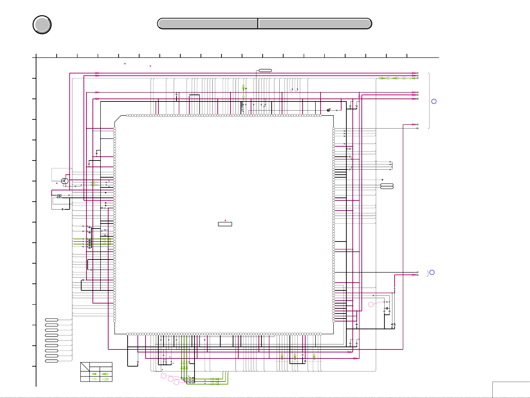
TY-20 BOARD (1/4)
TY-20 BOARD (1/4)
(CAMERA DSP, MAIN CPU)
(CAMERA DSP, MAIN CPU)
4-2. SCHEMATIC DIAGRAMS
PD-174 BOARD
PD-174 BOARD
(LCD DRIVE, CONTROL SWITCH)
(LCD DRIVE, CONTROL SWITCH)
DSC-U30
TY-20 BOARD (2/4)
TY-20 BOARD (2/4)
TY-20 BOARD (3/4)
TY-20 BOARD (3/4)
TY-20 BOARD (4/4)
TY-20 BOARD (4/4)
COMMON NOTE FOR SCHEMATIC DIAGRAMS WAVEFORMS
COMMON NOTE FOR SCHEMATIC DIAGRAMS WAVEFORMS
(MEMORY, CONNECTOR)
(MEMORY, CONNECTOR)
(LENS DRIVE)
(LENS DRIVE)
(HI CONTROL)
(HI CONTROL)
DD-209 BOARD (1/2)
DD-209 BOARD (1/2)
DD-209 BOARD (2/2)
DD-209 BOARD (2/2)
(DC IN, REGULATOR)
(DC IN, REGULATOR)
(DC/DC CONVERTER)
(DC/DC CONVERTER)
Page 18
COVER
COVER
For Schematic Diagram
• Refer to page 4-39 for printed wiring board.
• Refer to page 4-58 for waveforms.
1
TY-20 BOARD (1/4)
A
CAMERA DSP, MAIN CPU (TRS BLOCK 1/2)
B
C
D
E
Q601
UNRL11300AS0
4
1
X601
48MHz
XDP_PULL_UP
3
2
USB_CLK_EN
C614
0.1u
R601
0
F
G
H
I
J
K
L
M
N
O
LND601
LND602
LND603
LND604
LND605
LND606
LND607
LND608
LND609
RTCK
TCK
TDO
TDI
TMS
XTRST
XRESET_JTAG
232C_TXD
232C_RXD
P
05
MC_A01
MC_A02
USB_D-
USB_D+
R612
1k
USB_HOLD
USB_SUSPEND
USB_VBUS
IRIS_CONT1
HALL_GAIN
HALL_OFFSET
HALL_AD
LENS_TEMP
VR
VG
VB
VP
MC_A03
MC_A04
MC_A05
MC_A06
MC_A07
MC_A08
MC_A09
MC_A10
MC_A11
MC_A12
MC_A13
MC_A14
MC_A15
MC_A16
MC_A17
MC_A18
MC_A19
MC_A20
R604
1k
R605
1k
R607
R608
1k
R609
R610
1k
C609
XX
SIGNAL PATH
REC
PB
32
C613
0.1u
C611
0.1u
USB
R617
USB
R618
C616
0.1u
C602
0.1u
R616
C603
0.1u
C605
1k
XX
XX
C606
1k
XX
C607
C608
XX
XX
C601
VIDEO SIGNAL
CHROMA
Y/CHROMA
DSC-U30
4-2. SCHEMATIC DIAGRAMS TY-20 BOARD
4-2. SCHEMATIC DIAGRAMS TY-20 BOARD
56 11
:Voltage measurment of the CSP ICs
and the Transistors with mark,are
not possible.
MC_XRD
MC_XCS0
MC_CE1R
MC_XWE1
303304
NC
DACK
DREQ
PIPESTAT[1]
VDD
VDDQ
PIPESTAT[0]
TRACEPKT[7]
VSS
TRACEPKT[6]
TRACEPKT[5]
TRACEPKT[4]
TRACEPKT[3]
TRACEPKT[2]
TRACEPKT[1]
VDDQ
TRACEPKT[0]
TRACESYNC
TRACECLK
VDD
A0
A1
A2
VSS
AVDD(USB 3.1V)
D-
D+
AVSS
VDDQ(USB 3.1V)
HOLD
UCLK
VSS
VDD(USB_1.5V)
SUSPEND
VBUS
AVDD
IRIS_CONT1
IRIS_CONT2
HALL_GAIN
HALL_OFFSET
AVSS
AVSS
HALL_AD
NC
LENS_TEMP
CCD_TEMP
AN[3]
VR
VG
VB
VP
AVDD
VDD
A3
A4
VSS
A5
A6
A7
VDDQ
A8
A9
A10
VDD
A11
A12
A13
VSS
A14
A15
A16
NC
VDDQ
A17
A18
NC
A19
A20
A21/PK[3]
A22/PK[4]
PIPESTAT[2]
VSS
VDDQ
A25/PK[7]
A23/PK[5]
A24/PK[6]
79
77 78
80 81 82 83 84 85 86 87 88 89 90 91 92
C617
0.1u
12345678
910111213141516171819202122
27
0.5%
2324252627282930313233343536
27
0.5%
CL601
CL602
CL603
R615
47k
47k
4351 4250 4149 4048 3947 3846 3745
44
52
53545556575859606162636465
6667686970717273747576
SDRAM_XCAS
SDRAM_XRAS
(AU_LRCK)
(IRIS_CONT)
NC
MC_XWE0
VDD
TO0/PE[2]
PANEL_V
MC_XWE1
PANEL_V
LCD_CK
VSS
VDDQ
CS4/PJ[2]
LCD_CKHDEXTPAL
HDD
SYS_V
289290291292293294295296297298299300301302
CS5A/PJ[3]
SRRAM_XCS
VSS
SYS_V
0R625
R627
22k
0.5%
3
BS
MC_XCS0
IRF1
VRF
93 94 95 96
0
R688
0.5%
33k
R626
C651
0.1u
2
C619
0.1u
RD
SDRAM_RDXWR
AVSS
IRF0
0R689
R628
27k
0.5%
1
813184
MC_D00
MC_D01
MC_D02
C620
0.1u
D1
D2
D0
VDD
VDDQ
WAIT
SDRAM_CKO
SDRAM_CKE
AVDDQ
CV_OUTBOROGOSTRB_AD
97 98 99 100 101 102103 104 105106 107
AVSS
AVDDQ
C621
0.1u
R690
1500
0.5%
R691
R692
9
MC_D03
MC_D04
MC_D05
MC_D06
MC_D07
MC_D08
MC_D09
274275276277278279280281282283284285286287288
D4
D3
VSS
VSUB_CNT
VDD
VSS
0
R633
STRB_ON
1500
1500
D7
D8
D9
D5
D6
VDDQ
STRB_ON
VDDQ
MSHUT_ON
DIR2A
EN2
DIR2B
108109 110 111112 113 114115 116 117118 119 120121
MSHUT_ON
0.5%
0.5%
MC_D10
MC_D11
NC
D10
IC602
CAMERA DSP
MAIN CPU
IC602
CXD3159GA-T6
XOVF_RST_SENS
DIR1B
PANEL_B
PANEL_G
MS_BS
MC_D12
D11
DIR1A
PANEL_R
MS_DIO
MC_D13
MC_D14
MC_D15
MS_SCLK
MS MS
22
XX
R637
R636
260261262263264265266267268269270271272273
D15
D14
D13
D12
VSS
VDD
MSDIO
MSSCLK
DIR0BNCEN0
VSS
VDD
DIR0A
EN1
XZM_RST_SENS
122123 124 125126 127 128129 130 131132 133 134135
PE_EN0
PE_DIR0A
PE_DIR0B
FB601
100
R639
VDDQ
ACCESS_LED
XFC_RST_SENS
CKTGO
XFC_RST_SENS
TG_CLK
22
R642
RXD1
MSBS
CCDFD
CKTGI
MCK
CA_FD
127 15
LND610
FR_SI
FR_SO
XCAM_SCK
0
R646
CAM_SCK
VSS
CA_HD
XX
R681
TXD_TO_FR
RXD_FROM_FR
CCDHD
DUMCLP
XFR_SCK
XCS_MC
EEPROM_RXD
246247248249250251252253254255256257258259
VSS
FR_SCK
XCS_MC
CTS5/PO[6]
VDD
OPBCLP
CAMVDI
ADIN[11]
136137 138 139140 141 142143 144
CA_AD10
CA_AD11
VDDR
EEPROM_RXD
ADIN[10]
ADIN[9]
CA_AD09
EEPROM_TXD
EEPROM_SCK
EEPROM_SCK
ADIN[8]
CA_AD07
CA_AD08
EEPROM_RXD
R647
RXD4/PO[0]
EEPROM_TXD
VSS
ADIN[7]
232C_RXD
XX
TXD4/PO[0]
ADIN[6]
CA_AD06
232C_TXD
EEPROM_TXD
R648
XX
CTS4/PO[3]
ADIN[5]
CA_AD04
CA_AD05
RTS4_SCK4/PO[2]
ADIN[4]
MC_CE2R
VDDQ
USB_D+PULLUP
STRB_PHOTO_ON
VDD
145146 147 148149 150
0.1u
C622
C623
0.1u
CAM_SO
CAM_SO
VDDQ
1410 19
MS_POWER_ON
D902
SML-310LTT86
(MS ACCESS)
R908
330
229230
231232233234235236237238239240241242243244245
VSS
VDDR
TG_WEN
AMP_ON
MSHUT_EN
MS_PWR_ON
CAM_DD_ON
XCAM_RST
XFE_CS
XTG_CS
NC
BB_PS
XEEPROM_CS
VDDQ
221222 223 224225 226 227228
NC
EEPROM_RST
XLCD_TG_CS
VSS
VDDR
XLENS_RST_LED
XMC_HELP
XSYS_RESET
TREQB
TREQA
SCAN_ENABLE
TMODE
AE_LOCK_LED
CA_AD03
ADIN[3]
(XAU_LINE_MUTE)
(USB_D+PULLUP)
VSS
NCNCVDDQ
ADIN[2]
ADIN[1]
151152
CA_AD01
CA_AD02
(CAM_DD_ON1)
EEPROM_BUSY
XZM_RST_SENS
XFC_RST_SENS
NTSC/PAL
SC/PN[6]
RDY/PN[7]
XWP/PN[5]
XRE/PN[4]
XWE/PN[3]
ALE/PN[2]
CLE/PN[1]
XCE/PN[0]
FD0/PC[0]
FD1/PC[1]
FD2/PC[2]
FD3/PC[3]
FD4/PC[4]
FD5/PC[5]
FD6/PC[6]
FD7/PC[7]
INT3/PF[3]
INT2/PF[2]
WAKEUP
PLLMD[2]
PLLMD[1]
PLLMD[0]
ADIN[0]
CA_AD00
207208 209 210211 212 213214 215 216217 218 219220
VSS
VDDR
RTCK
TCK
VDDQ
TDO
TDI
TMS
193194 195 196197 198 199200 201 202203 204 205206
NC
TRST
VSS
VDDQ
VDDR
178179 180 181182 183 184185 186 187188 189 190191 192
VSS
VDDR
(SYSV)
VDDQ
164165 166 167168 169 170171 172 173174 175 176177
OSCO
OSCI
VSS
PVSS
PVDD
PVSS
PVDD
PVSS
PVDD
153154 155 156157 158 159160 161 162163
16
C629
C625
0.1u
0.1u
0R657
0R658
0R659
R687
1k
C632
0.1u
C628
0.1u
C627
XX
C630
0.1u
C626
C631
XX
XX
4-11 4-12
XCAM_RESET
XGCAM_CS
XCS_EEPROM
EEPROM_RST
XCS_PANEL_TG
XLENS_RST_LED
XMC_HELP
EEPROM_BUSY
XFC_RST_SENS
XMC_NMI
R663
XTG_CS
4
17
USB_3.1V
MS MS USB
R666
0
XRESET_JTAG
XRST_SYS
R667 2200
R685
47k
CL604
LND612
LND613
RTCK
TCK
TDO
TDI
TMS
XTRST
L604
10uH
0
R665
1M
X603
27MHZ
C633
5p
C634
7p
C650
C649
22u
0.1u
4V
USB_1.5V
1
D_1.5V_1
D_1.5V_2
D_2.8V_1
A_2.8V_1
CAM_DD_ON
REG_GND
D_2.8V
1
(2/4)
2
(2/4)
TY-20 (1/4)
Page 19

DSC-U30
For Schematic Diagram
• Refer to page 4-39 for printed wiring board.
COVER
COVER
4-2. SCHEMATIC DIAGRAMS TY-20 BOARD
4-2. SCHEMATIC DIAGRAMS TY-20 BOARD
1
TY-20 BOARD (2/4)
A
MEMORY, CONNECTOR(TRS BLOCK 2/2,CN BLOCK)
XX MARK:NO MOUNT
NO MARK:REC/PB MODE
1
3 16
MS MS
B
1
C
D
E
F
G
H
I
J
K
L
05
(1/4)
FP-532
FLEXIBLE
LND101-151
(PAGE 4-32)
SIGNAL PATH
REC
PB
7
(4/4)
VIDEO SIGNAL
CHROMA
A_2.8V_1
USB_3.1V
USB_1.5V
D1.5V_1
D1.5V_2
D2.8V_1
CAM_DD_ON
EVER_4.0V
EVER_3.0V
Y/CHROMA
LND611
VL_3V
CN901
BUZZER_15V
FAST_CHARGE
USB_UNREG_SW
SYS_DD_ON
UNREG_SCK
UNREG_SO
XCS_DDCON
EVER_3.0V
EVER_4.0V
EVER_4.0V
DD_CON_SENS
BATT_UNREG
ACV_UNREG
PANEL_13.5V
PANEL_13.5V
PANEL_2.8V
PANEL_2.8V
CAM_DD_ON
CAM_-7.5V
CAM_-7.5V
ST_UNREG
ST_UNREG
ST_UNREG
BUZZER
USB_5V
USB_5V
REG_GND
REG_GND
REG_GND
REG_GND
REG_GND
REG_GND
REG_GND
REG_GND
REG_GND
REG_GND
REG_GND
FL_-VO
D_2.8V
D_2.8V
A_2.8V
A_2.8V
D_1.5V
D_1.5V
D_1.5V
CAM_15V
CAM_15V
REG_GND
REG_GND
51P
51
50
49
48
47
46
45
44
43
42
41
40
39
38
37
36
35
34
33
32
31
30
29
28
27
26
25
24
23
22
21
20
19
18
M_5V
17
M_5V
16
15
14
13
12
11
10
9
8
7
6
5
4
3
2
1
USB
BUZZER_15V
BUZZER
USB_5V
FAST_CHARGE
USB_UNREG_SW
SYS_DD_ON
UNREG_SCK
UNREG_SO
XCS_DDCON
DD_CON_SENS
BATT_UNREG
ACV_UNREG
R906
XX
4
52
IC603
16M FLASH ROM
IC603
MB84VD2139
3
(4/4)
R905
XX
LND901
STATIC_GND
R907
XX
R909
0
FB902
C901
10u
6.3V
10uH
CAM_DD_ON
ST_UNREG
C908
10u
6.3V
C902
C903
22u
3.3u
16V
35V
L903
10uH
4
(3/4)
L904
C904
10u
10uH
6.3V
L902
6
:Voltage measurment of the CSP ICs
and the Transistors with mark,are
not possible.
R669
47k
MC_A08
MC_XWE1
MC_A09
MC_A12
MC_A04
MC_A07
XRST_SYS
MC_CE2R
MC_A20
MC_A13
MC_A16
MC_A03
MC_A06
MC_A19
MC_A10
MC_A14
MC_A02
MC_A05
MC_A18
MC_11
MC_A15
MC_A01
MC_A17
MC_XRD
7118
NC
A8
A7
B2
LB
B3
WP/ACC
B4
WE
B5
A8
B6
A11
B7
A3
C1
A6
C2
UB
C3
RESET
C4
CE2r
C5
A19
C6
A12
C7
A15
C8
A2
D1
A5
D2
A18
D3
RY/BY
D4
NC
D5
A9
D6
A13
D7
NC
D8
A1
E1
A4
E2
A17
E3
A10
E6
A14
E7
NC
E8
A0
F1
9
NC
K8
NC
K1
DQ14
J7
DQ5
J6
NC
J5
DQ11
J4
DQ2
J3
DQ8
J2
Vss
H8
DQ7
H7
DQ12
H6
Vccr
H5
Vccf
H4
DQ10
H3
DQ0
H2
CE1r
H1
Vccf
G8
DQ15
G7
DQ13
G6
DQ4
G5
DQ3
G4
DQ9
G3
OE
G2
CEf
G1
A16
F8
NC
F7
DQ6
F6
DQ1
F3
Vss
F2
C637
0.1u
MC_D14
MC_D05
MC_D11
MC_D02
MC_D08
MC_D07
MC_D12
C635
0.1u
MC_D10
MC_D00
MC_CE1R
MC_D15
MC_D13
MC_D04
MC_D03
MC_D09
47kR670
MC_XCS0
MC_D06
MC_D01
C638
10u
6.3V
IC605
USB_1.5V REG
IC605
S-817A15ANB-CUE-T2
NC
4
VOUT
3
1.5 3.1
C636
10u
6.3V
XCS_EEPROM
EEPROM_SCK
EEPROM_TXD
EEPROM_RXD
EEPROM_RST
EEPROM_BUSY
10
FB602
C643
22u
4V
C641
L605
0.1u
4.7uH
L601
C640
22u
FB603
4V
R673
XX
2.9
1
2.9
2
0R671
3
4
R672
0
1
VSS
2
VIN
C642
0.1u
C644
10uH
22u
4V
IC604
EEPROM
IC604
AK6417CH-E2
EEPROM_BUSY
VCC
RST
GND
CS
SCK
2.9
DI
1
DO
C645
10u
6.3V
12 18
C646
2.9
0.1u
8
2.9
7
6
5
3
2.9
45
100k
R674
C639
L602
22u
4V
10uH
C647
123
0.1u
4
3.1
D_2.8V
REG_GND
13
265
(1/4) (4/4)(3/4)
IC606
USB_3.1V REG
IC606
RN5RZ31BA-TL-FA
A_2.8V
M_5V
8
(3/4)
USB_PWR_ON
14
USB_SUSPEND
USB_PWR_ON
USB_CLK_EN
USB_HOLD
USB_VBUS
FR_SI
FR_SO
XFR_SCK
XCS_MC
XMC_HELP
XDP_PULL_UP
SYS_V
XMC_NMI
XRST_SYS
MS_POWER_ON
MS_SCLK
MS_DIO
MS_BS
USB_D-
USB_D+
CA_AD11
CA_AD7
CA_AD3
CA_AD010
CA_AD6
CA_AD2
CA_AD9
CA_AD5
CA_AD1
CA_AD8
CA_AD4
CA_AD0
XTG_CS
XCAM_CS
CAM_S0
XCAM_SCK
MCK
TG_CLK
CA_FD
CA_HD
XCAM_RESET
XRESET_SW_ON
XPWR_LED
XPWR_ON
MODE_DIAL
KEY_AD0
XCHARGE_LED
TG_CLK
XCS_LCD
XVD
XHD
XRST_SYS
PANEL_R
PANERL_G
PANEL_B
VP
VB
VR
VG
15
10
(4/4)
CN902
31
CD_GND
30
CA_AD11
29
CA_AD7
28
CA_AD3
27
CA_AD10
26
CA_AD6
25
CA_AD2
24
CA_AD9
23
CA_AD5
22
CA_AD1
21
CA_AD8
20
CA_AD4
19
CA_AD0
18
XTG_CS
XCAM_CS
17
16
CAM_SO
15
XCAM_SCK
CD_GND
14
MCK
13
12
CD_GND
TG_CLK
11
CD_GND
10
CA_FD
9
CA_HD
8
XCAM_RESET
7
6
TG3V
DRV3V
5
FE3V
4
CAM_-7.5V
3
2
1
CN904
XRESET_SW_ON (N.C.)
1
XPOWER_LED (N.C.)
2
XPOWER_ON (N.C.)
3
MODE_DIAL (N.C.)
4
KEY_AD0
5
VL_3V
6
XCHARGE_LED
7
D_2.8V
8
REG_GND
9
TG_CLK
10
REG_GND
11
XCS_LCD
12
XLCD_SCK
13
LCD_SO
14
XVD
15
XHD
16
XRST_SYS
17
REG_GND
18
PANEL_R
19
PANEL_G
20
PANEL_B
21
REG_GND
22
23
VP
24
VB
25
VR
26
VG
PANEL_2.8V
27
PANEL_2.8V
28
PANEL_13.5V
29
PANEL_13.5V
30
REG_GND
31
FL_+VO
32
FL_-VO
33
CAM_15V
CD_GND
31P
33P
HALL_AD
HALL_OFFSET
IRIS_CONT1
HALL_GAIN
XFC_RST_SENS
XLENS_RST_LED
PE_EN0
PE_DIR0B
PE_DIR0A
MSHUT_ON
STRB_ON
LENS_TEMP
XRESET_SW_ON
XPWR_LED
XPWR_ON
MODEL_DIAL
KEY_AD0
XCHARGE_LED
USB_SUSPEND
USB_PWR_ON
USB_CLK_EN
USB_HOLD
USB_VBUS
FR_SI
FR_SO
XFR_SCK
XCS_MC
XMC_HELP
XDP_PULL_UP
SYS_V
XMC_NMI
XRST_SYS
MS MS
USB
USB_D-
USB_D+
USB
MS_POWER_ON
MS_SCLK
MS_DIO
MS_BS
15
(4/4)
CL901
9
(4/4)
17
HALL_AD
HALL_OFFSET
IRIS_CONT1
HALL_GAIN
XFC_RST_SENS
XLENS_RST_LED
PE_EN0
PE_DIR0B
PE_DIR0A
MSHUT_ON
STRB_ON
LENS_TEMP
XRESET_SW_ON
XPWR_LED
XPWR_ON
MODEL_DIAL
KEY_AD0
XCHARGE_LED
CD-425
FLEXIBLE
LND101-131
(PAGE 4-9)
FP-533
FLEXIBLE
LND101-133
(PAGE 4-31)
11
(3/4)
12
(3/4)
13
(4/4)
(2/2)
TY-20 (2/4)
4-13 4-14
Page 20

COVER
COVER
For Schematic Diagram
• Refer to page 4-39 for printed wiring board.
4-2. SCHEMATIC DIAGRAMS TY-20 BOARD
4-2. SCHEMATIC DIAGRAMS TY-20 BOARD
DSC-U30
1
TY-20 BOARD (3/4)
A
LENS DRIVE(LD BLOCK)
XX MARK:NO MOUNT
NO MARK:REC/PB MODE
R:REC MODE
P:PB MODE
B
C
D
E
F
G
H
I
J
D201
1SS401(TE85L)
D202
MA4L11100AS0
R253
0
14
3
C231
1u
105
1
2
3
4
5
R901
6
7
22k
8
9
10
11
12
13
14
15
16
17
18
19
20
21
22
23
24
25
B3_ZA
32
R219
330
0.5%
18
PGND
R208
Q204
1
4
16
17
B4_ZB
3
R213
10k
0.5%
C206
1u
1k
R212
100k
C205
0.1u
0.9
12
13
14
OUT
IN(-)
R1/P0.1
R0.9/P1.1
OUT2IN(-)3IN(+)4VCC5IN(+)6IN(-)7OUT
1
0.7
0.1
R222
22k
13
14
15
IN3
IN4
EN3
EN4
0.5%
11
IN(+)
0.1
R228
12k
R227
1200
R211
4700
0.5%
0.9
0.9
9
10
GND
IN(-)
IN(+)
2.9
0.9
XX
C213
R232
10k
IC204
SHUTTER DRIVE,
FOCUS DRIVE
IC204
WTGA-UPD16877W
67
1200R233
R220
R234
150k
0.5%
R229
1200
0.5%
R215
47k
0.5%
R231
180k
0.5%
C212
0.001u
0.9
8
OUT
0.9
1.1
C214
0.01u
IC206
IRIS DRIVE,
HALL AMP
IC206
LMV324MTX
R242
24k
0.5%
R241
C237
10k
0.1u
0.5%
R254
0
C238
10u
C233
0.1u
13
14
0.9
0.9
OUT
IN(-)
R0.8/P1.5
OUT1IN(-)2IN(+)3VCC4IN(+)5IN(-)6OUT
1
0.9
0.9
C208
0.033u
R214
100k
0.5%
C207
3300p
3
2
1
Q201
2SB1462L0AS0
D_2.8V SWITCH
L202
R239
220
12
R226
1k
16k
0.5%
C211
0.01u
0.5%
R230
180k
R224
22k
0.5%
C218 0.022u
9
10
11
GND
IN(-)
IN(+)
IN(+)
R0.8/P2.7
R0.8/P1.7
R0.9/P2.9
2.9
R0.8/P2.9
R0.8/P2.9
R0.8/P2.9
0.1u
C217
4
10uH
C215
0.5%
0.1u
R223
100k
0.5%
R225
100k
0.5%
C210
0.022u
8
OUT
7
C216
XX
R205
56k
4700R206
FB202
24 9
Q202
2SD2216L0AS0
IRIS DRIVE
2
3
1
4
C203
0.022u
R207
10
IC202
IRIS DRIVE,
HALL BIAS CONTROL,
HALL GAIN CONTROL
IC202
NJM12902V(TE2)
2SD2216L0AS0
R255
0
GAIN CONTROL
C209
0.1u
2
19
20
21
22
23
24
VDD
PGND
B2_FB
B1_FA
VM2_3
VM12A1_FA3PGND4A2_FB5A3_ZA6PGND7A4_ZB8VM49IN110EN111IN212EN2
1
8
:Voltage measurment of the CSP ICs
and the Transistors with mark,are
not possible.
L201
10uH
C219
10u
6.3V
Q901
RN4983FE(TPLR3)
M_5V SWITCH
R0/P5
5
4
3
R5/P05
6
1
R0/P5
2
R2.9/P0
A_2.8V
M_5V
D_2.8V
REG_GND
HALL_AD
HALL_OFFSET
HALL_GAIN
IRIS_CONT1
XFC_RST_SENS
XLENS_RST_LED
PE_EN0
PE_DIR0B
PE_DIR0A
MSHUT_ON
CAM_DD_ON
ST_UNREG
ST_UNREG
ST_UNREG
ST_UNREG
STB_CHARGE
REG_GND
REG_GND
REG_GND
XSTB_FULL
M_5V
STRB_ON
DRIVE-
DRIVE+
HALL-
BIAS+
BIAS-
HALL+
XFC_RST_SENS
F_SENS_VCC
F_SENS_GND
N.C.
LENS_TEMP
FOCUS_B
FOCUS_A
FOCUS_B
FOCUS_A
11
12
8
(2/4)
5
(2/4)
11
(2/4)
4
(2/4)
25PCN903
SL-59
FLEXIBLE
LND601-625
(PAGE 4-25)
K
05
LENS_TEMP
STB_ON
XSTB_FULL
STB_CHARGE
4-15 4-16
12
(2/4)
14
(4/4)
TY-20 (3/4)
Page 21

DSC-U30
For Schematic Diagram
• Refer to page 4-39 for printed wiring board.
• Refer to page 4-58 for waveforms.
COVER
COVER
1
4-2. SCHEMATIC DIAGRAMS TY-20 BOARD
4-2. SCHEMATIC DIAGRAMS TY-20 BOARD
2
4 14
5
8
9
10
11
12
13
15 173
1667
TY-20 BOARD (4/4)
A
HI CONTROL(FR BLOCK)
XX MARK:NO MOUNT
NO MARK:REC/PB MODE
B
BUZZER_15V
BUZZER
USB_5V
FAST_CHARGE
USB_UNREG_SW
SYS_DD_ON
3
UNREG_SCK
13
(2/4)
(2/4)
14
(3/4)
(2/4)
9
UNREG_SO
XCS_DDCON
DD_CON_SENS
BATT_UNREG
ACV_UNREG
XRESET_SW_ON
XPWR_LED
XPWR_ON
MODE_DIAL
KEY_AD0
XCHARGE_LED
STB_CHARGE
XSTB_FULL
USB_SUSPEND
USB_PWR_ON
USB_CLK_EN
USB_HOLD
USB_VBUS
XFR_SCK
XCS_MC
XMC_HELP
XDP_PULL_UP
XMC_NMI
XRST_SYS
C
D
E
F
G
H
I
US-7
FLEXIBLE
LND050-057
(PAGE 4-27)
J
15
(2/4)
REG_GND (N.C.)
USB_D+
USB_D-
K
EVER_3.0V
7
EVER_4.0V
(2/4)
REG_GND
L
6
(2/4)
FR_SI
FR_SO
SYS_V
VL_3V
D_2.8V
CN907
:Voltage measurment of the CSP ICs
and the Transistors with mark,are
not possible.
SIGNAL PATH
VIDEO SIGNAL
Y/CHROMA
REC
PB
6PCN908
RS-85
FLEXIBLE
LND001-006
(PAGE 4-31)
MS_POWER_ON
MS MS
MSMS
MS_SCLK
MS_DIO
MS_BS
23
MS_VSS
22
MS_VCC
21
MS_VCC
20
MS_SCLK
19
MS_INT
18
MS_DIO
17
MS_VCC (N.C.)
16
MS_VCC (N.C.)
15
MS_BS
14
MS_VSS
13
GND
12
MODE_DIAL
XSHUTTER
11
10
XAE_LOCK_SW
9
XPOWER_ON
8
GND
7
D_2.8V
6
XPOWER_LED
5
XLENS_CAP_OPEN
4
D_2.8V
3
XSELF_TIMER_LED
2
XTALLY_LED (N.C.)
1
XAE_LOCK_LED (N.C.)
23PCN906
10
(2/4)
SW-376
FLEXIBLE
LND001-023
(PAGE 4-29)
BUZZER
C407
0.47u
2
BUZZER
FAST_CHARGE
USB_UNREG_SW
SYS_DD_ON
UNREG_SCK
UNREG_SO
XCS_DDCON
DD_CON_SENS
BATT_UNREG
ACV_UNREG
XRESET_SW_ON
XPWR_LED
XPWR_ON
MODE_DIAL
KEY_AD0
XCHARGE_LED
STB_CHARGE
XSTB_FULL
USB_SUSPEND
USB_PWR_ON
USB_CLK_EN
USB_HOLD
USB_VBUS
FR_SI
FR_SO
XFR_SCK
XCS_MC
XMC_HELP
XDP_PULL_UP
SYS_V
XMC_NMI
XRST_SYS
8P
8USB_GND
7USB_GND
6USB_D-
5USB_D+
4
3USB_5V
2USB_5V
1USB_JACK_IN
USB
USB
XPWR_ON
XLENS_CAP_OPN
XSHTR_ON
XAE_LOCK_SW
Q401
SSM3K03FE(TPL3)
INVERTER
XTALLY_LED
XCHARGE_LED
XPWR_LED
XSELF_TIMER_LED
UNREG_SO
XRESET_SW_ON
R402
470k
Q403
2SD2216L0AS0
INVERTER
2.8
R401
R460
1k
0
0
0
1
4
2
5
6
3
RN1904FE(TPLR3)
1.9
1.8
0
Q402
LED DRIVE
R406
1k
C401
4.7u
10V
R404
470k
3
2
1
4
470kR403
C403
4700p
C402
4.7u
10V
470k
R405
XRESET
R409
470k
R411
1M
R408
1k
470k
470k
470k
470k
R407
R410
R458
R414
47k
C404
10u
6.3V
R412
C406
0.1u
C422
10u
6.3V
R418
33k
Q404
2SD2216L0AS0
MODULATOR
R415
R461
R416
1k
R417
C405 0.1u
R413
470
L401
47uH
3
1
4
UNRL21300AS0
MODULATOR
1k
1k
1k
3
3
4
3
1234567891011121314151617181920
5678
CS
RESET
VOUT
VBAT
VCH
VIN
VRO
VSS
XMC_NMI
R419
100k
3
4
Q405
XPWR_ON
XPB_ON
XLENS_CAP_OPN
XSHTR_ON
XAE_LOCK_ON
MS_IN
XLANC_PWR_ON
BATT/XEXT
XUSB_JACK_IN
LANC_JACK_IN
AV_JACK_IN
LCD_COM/XDATA
GND
BACK_UP_VCC
XTALLY_LED
CHARGE/STB_LED
XPWR_LED_ON
XLANC_ON
SELF_TIMER_LED
UNREG_SO
USB_PWR_ON
R421
XX
2
1
470kR425
MELODY
USB_PWR_ON
MC_WAKE_UP
FR_SI
XCS_DDCON
UNREG_SCK
21 22 23 24 25 26 27 28 29 30 31 32 33 34 35 36 37 38 39 40
5
R423
R424
470
470
R420
100k
XCS_DDCON
UNREG_SCK
FR_SI
FR_SO
IC402
INITIAL RESET,
R422
100k
1234
BACK UP VCC
BD4201FV-E2
3
2.9
R428
33
C408
C423
0.1u
3300p
XRST_SYS
XRST_SYS
FR_SO
XFR_SCK
IC402
SYS_DD_ON
0
R426
SYS_DD_ON
XFR_SCK
XCS_MC
R429
330
XRESET
USB_CLK_EN
USB_UNREG_SW
XRESET
USB_CLK_EN
XSTB_PWRSAVE
IC401
HI CONTROL
MB89097LGA-G-136-ER
MOD0
10MHz_IN
XCS_MC
R430
1M
X401
10MHz
D402
MA2SD24008S0
R433
1M
0.5%
C410
0.1u
(AN13)
DRY_BATT_IN1
USB_UNREG_SW
IC401
10MHz_OUT
BATT_IN
MOD1
C409
0.1u
ACV_UNREG
0.5%
1MR431
DEW_SENS
SYS_V
470k
R432
SYS_V
USB_SUSPEND
USB_UNREG_SW
BATT_UNREG
DD_CON_SENS
C411 0.47u
0.5%
1M
R434
ACV_SENS
BATT_SENS
XSTB_FULL
USB_SUSPEND
1kR437
470k
R435
XSTB_FULL
USB_HOLD
R436
1M
0.5%
1k
R438
0.01u
C412
AVss
USB_HOLD
DD_CON_SENS
XMC_HELP
XSETUP_ON
Program_Dial_A
470k
R439
XMC_HELP
3.3
3
0
4
C413
0.1u
AVREF
Program_Dial_B
LANC_IN
VOUT
CE
USB_VBUS
6162636465666768697071727374757677787980
AVCC
USB_VBUS
ZOOM_AD_KEY
KEY_AD4
KEY_AD3
KEY_AD2
KEY_AD1
KEY_AD0
MODE_DIAL
BACK_UP_VCC
32kHz_IN
32kHz_OUT
XDP_PULL_UP
FAST_CHARGE
INIT_CHARGE
STB_CHG
XSTB_POPUP
XCS_LCD
BATT_SI
BATT_SO
(RESERVED)
LANC_OUT
LANC_IN
470k
R442
LANC_OUT
IC403
3.3V REG
IC403
RQ5RW33AA-TR-FA
1 XRESET_SW_ON
2 REG_GND
3 XCPC_IN (N.C.)
4 EVER_4.0V (N.C.)
5 LANC_IN (N.C.)
6 LANC_OUT (N.C.)
6
10k
R453
10k
R454
10k
XXC418
C419
R443
XX
10M
51 52 53 54 55 56 57 58 59 60
GND
50
41 42 43 44 45 46 47 48 49
4
2
VIN
GND
1
X403
150k
32.768kHz
R444
C909
22u
4V
R902
2200
R455
KEY_AD0
10k
R451
1kR449
1kR450
C420
9p
C421
9p
C907
0.47u
2.9
MODE_DIAL
10k
R452
R459
10k
XDP_PULL_UP
FAST_CHARGE
STB_CHARGE
MS_SCLK
MS_DIO
MS_BS
D901
MA4L11100AS0
R904
470k
2.9
3
1
6
Q902
SSM6E01TU
B+ SWITCH
2
45
14
C905
3
22u
2.9
4V
0
2
R903
3300
MS_SCLK
MS_DIO
MS_BS
C906
0.1u
MODE_DIAL
XSHTR_ON
XAE_LOCK_SW
XPWR_ON
XPWR_LED
XLENS_CAP_OPN
XSELF_TIMER_LED
XTALLY_LED
TY-20 (4/4)
05
4-17 4-18
Page 22

COVER
COVER
For Schematic Diagram
• Refer to page 4-41 for printed wiring board.
• Refer to page 4-59 for waveforms.
4-2. SCHEMATIC DIAGRAMS PD-174 BOARD
4-2. SCHEMATIC DIAGRAMS PD-174 BOARD
DSC-U30
PD-174 BOARD
LCD DRIVE,CONTROL SWITCH
A
(RGB/TG BLOCK,
SWITCH BLOCK)
XX MARK:NO MOUNT
NO MARK:REC/PB MODE
:Voltage measurment of the CSP ICs
B
and the Transistors with mark,are
not possible.
(Note)Resistors are mounted to the location
where L402 and L403 are printed.
C
CN401
29P
D
E
FP-533
FLEXIBLE
LND001-029
(PAGE 4-31)
F
G
H
I
J
K
XCHARGE_LED
PANEL_13.5V
PANEL_13.5V
BT480
LITHIUM BATTERY
SECONDARY
KEY_AD0
VL_3V
D_2.8V
REG_GND
TG_CLK
REG_GND
XCS_LCD
XLCD_SCK
LCD_SO
XVD
XHD
XRST_SYS
REG_GND
PANEL_R
PANEL_G
PANEL_B
REG_GND
VP
VB
VR
VG
PANEL_2.8V
PANEL_2.8V
REG_GND
FL_+VO
FL_-VO
R480
680
29
28
27
26
25
24
23
22
21
20
19
18
17
16
15
14
13
12
11
10
9
8
7
6
5
4
3
2
1
STATIC GND
LND480
R401
22k
0.5%
SML-310YTT86
R402
12k
0.5%
4
D482
MAZR082H0AS0
3
5
76 16
81410
12
8
R412
TG59
0
TG43
TG42
TG41
139
SIGNAL PATH
VIDEO SIGNAL
174
183 151 112
CHROMA
XHD
XHI_SO
REC
PB
L403
0
D481
XCS_LCD
XHI_SCK
XHI_SO
XVD
XHD
XRST
R406
82k
0.5%
R407
82k
47k
R408 82k
R405
22k
0.5%
R403
22k
0.5%
S480
S481
R481
1k
1
R482
1500
S482
2
S483
R483
3300
4
D480
XX
3
VP
VB
0.5%
VR
0.5%R404
VG
0.5%
10uH
C401
22u
4V
MENU
SCENE
EXEC
1
C480
2
XX
(Note)
C413
4.7u
C415
0.1u
59
60
RPD F3
POFF E3
61
VR G3
62
TG63
L402
0
(Note)
XVD
R414
XX
R415
82k
0.5%
XCS_LCD
R409
0
L401
C402
0.1u
TG64
TG65
TG72
C404
0.01u
TG76
TG77
R416
0
0.5%
R410
0.01u
XX
C403
VP G4
63
EN G5
64
HCK2 G6
65
TRON G7
66
DETIN F7
67
XVD E7
68
LPF_ADJ D7
69
NONEG C7
70
N.C. C6
71
BIAS C5
72
RGT C4
73
N.C. D4
74
N.C. E4
75
LED F4
76
VCK F5
77
HST F6
78
XCS E6
79
TRAP_ADJ D6
80
TST1 D5
81
N.C. E5
N.C. A12VDD B13COM_IN C14GND D15BL E16VR_DC_DET F17VG G18VB H19N.C. J110VCC2 J211VP_DC_DET J312XVP.SAVE J413WIDE J514N.C. J615EXT_DA J716C-BG J817N.C. J918VDD H919XSCK G920XCLR F9
1
C409
0.1u
58
VCC3 D3
5
57
OSCI C3
56
VCO B3
C420
R430
55
1u
100
3
54
TEST2 B4
53
OPIN+ B5
C406
52
VDO B6
TST0 B7
IC401
LCD DRIVER
CXA3617GG-T4
R429
100
470k
R413
C408
0.01u
51
B_IN B8
IC401
0.01u
R418
15k
44
45
46
47
48
49
50
SI H8
HD E8
SO G8
R_IN C8
CLKIN F8
TEST3 D8
C417
1u
6
C410
0.01u
TG13
UNRL11300AS0
BACKLIGHT
CONTROL
43
HCK1 H6
R_INJECT H7
Q461
42
0
R417
XHI_SCK
41
DWN H5
0
R411
1
VSTA H4
VG_DC_DET H2
VB_DC_DET G2
COM_OUT C2
COM_DC A2
XSH.SAVE A8
XRST
1
R461
47k
R462
47k
GND H3
GND2 F2
PWM E2
VREF D2
OSCO B2
OPOUT A3
TEST1 A4
OPIN- A5
HDO A6
TSTEN A7
N.C. A9
GND B9
G_IN C9
XWRT D9
VCC1 E9
C405
XX
2
40
1uC418
39
38
C419
1u
37
36
35
34
33
32
31
30
29
28
27
R440
26
R441
25
XX
24
23
22
21
R424
1M
100k
4.7u
R439
C422
0
C407
0.01u
2
2
3
4
Q401
UNRL21300AS0
R438
R437
XX
XX
4
3
R463
150k
R464
120k
IC461
TA75S01F(TE85R)
-3.1 2.9
VCC
123
-8
-3.1 0
BACKLIGHT CONTROL
IC461
0
45
1
UNRL21300AS0
C461
0.01u
SWITCHSWITCH
0.8
3
4
Q402
2
R465
47
0.5%
2SB1218A-QRS-TX
-1.7
1
Q462
BACKLIGHT
DRIVE
47
R431
100
Q405
2SD2216L0AS0
R428
100
Q403-406
PSIG DRIVE
2SB1462L0AS0
R443
XX
R444
47k
1
2
C423
XX
16V
Q403
1
2
4
3
4
3
4
2
2SB1462L0AS0Q406
VB
Q404
2SD2216L0AS0
R445
47k
3
3
1
VR
C424
XX
TG65
2
1
4
VG
VP
R446
470k
TG59
TG41
TG76
TG63
TG42
TG13
TG77
TG64
TG43
TG72
Q408
MCH3310-TL-E
VDD SWITCH
0
1
RD3.3UM-T1B
13.513.5
C425
0.01u
3
2
D402
C426
0.1u
C427
1u
R447
1M
4
Q409
UNRL21300AS0
SWITCH
R450
150k
R449
820k
1
R448
2
68k
Q410
2SB1462L0AS0
REF VOLTAGE GEN.
C428
0.1u
C429
0.1u
4
3
27PCN402
27
TEST
26
COM
25
VST
24
VCK
23
EN
DWN
22
21
VDD
20
VSS
19
VDDG
18
VSSG
17
CS
16
WIDE
HST
15
14
REF
13
DSUT
12
CRext
11
HCK2
10
HCK1
9
PSIG
8
G
7
R
6
B
5
RGT
TEST2
4
LED_K
3
N.C.
2
LED_A
1
PANEL UNIT
LCD901
1inch
COLOR LCD
D901
BACKLIGHT
05
4-19
The components identified by mark 0 or dotted
line with mark 0 are critical for safety.
Replace only with part number specified.
4-20
Les composants identifiés par une marque 0 sont
critiques pour la sécurité. Ne les remplacer que
par une piéce portant le numéro spécifié.
PD-174
Page 23

DSC-U30
DD-209 (1/2)
COVER
COVER
For Schematic Diagram
• Refer to page 4-43 for printed wiring board.
DD-209 BOARD (1/2)
A
DC IN,REGULATOR
XX MARK:NO MOUNT
B
C056
0.1u
(0)
<3>
Q002
JL001
JL002
R008
C002
0.047u
0.022u
(2.4)
<0>
1M
R061
R007
C003
0
BATT_UNREG/+
BATT_GND/-
0
0
Q004
MCH3306-TL-E
(0)<2.4>
R010
330k
(0)
<2.4>
Q018
SSM3K03FE(TPL3)
R003
330k
2.5
LND001
R001
R002
470k
1M
STATIC_GND
Q001,004,018
SWITCH
(2.4)
<0>
(0)
<3>
Q001
SSM3K03FE(TPL3)
Q002,006
SWITCH
SSM3K03FE(TPL3)
BT901
BATTERY
TERMINAL
C
D
E
F
G
UNREG_1
UNREG_2
REG_GND
1
EVER_3.0V
(2/2)
EVER_4.0V
H
I
J
K
05
4-2. SCHEMATIC DIAGRAMS DD-209 BOARD
4-2. SCHEMATIC DIAGRAMS DD-209 BOARD
3 151 112
Q005
CPH6311-TL
USB_UNREG
SWITCH
(0)<4.8>
R011
470k
R009
10k
0
UN9213J-(TX).SO
SWITCH
(2.6)<2.9>
2.5
2.5
0
MCH3306-TL-E
D014 XX
R005
100k
R006
1M
C009
1500p
Q006
Q003
R022
10k
D015 XX
4
NO MARK:REC/PB MODE,BATTERY/USB POWER SUPPLY
R:REC MODE
P:PB MODE
( ):BATTERY POWER SUPPLY
< >:USB POWER SUPPLY
5
(0)<4.8>
6
1
4
2
3
0
R020
470k
R021
10k
(0)<3.7>
Q007
SSM3K03FE(TPL3)
SWITCH
D010
MA2SD24008S0
D002
CRG01(TE85L)
Q008
ECH8603-TL-E
(2.5)
<3.8>
D003
XX
(-3.9)<3.5>
C010
(2.7)<0>
5
(2.5)
<3.7>
(-3.9)
<3.7>
2
1
7
8
6
5
3
4
2.5
XX
R024
1M
2.5
1
2.5
2
R027
10k
Vout
Vin
(2.5)
<3.7>
(-3.9)
<3.7>
5
6
8
7
<-8>
IC002
VOLTAGE DETECT
4
2
(-3.9)<3.7>
(-8)
<3.7>
2
(3)
R030
1M
XC61CC1502NR
IC002
(2.5)
<3.8>
3
1
6
1
-8
ECH8603-TL-E
Q009
Q008,009
SWITCH
(3)<-8>
3
4
3
C014
XX
(2.7)
<0>
Q011
SSM3K03FE(TPL3)
SWITCH
Vss
NC
RN4983FE(TPLR3)
EMERGENCY
5
(0)<3>
(0)<3>
R031
10k
4
3
76 16
:Voltage measurment of the CSP ICs
and the Transistors with mark,are
not possible.
Q010
DETECT
FAST_CHARGE
USB_UNREG_SW
1.5V
1
2.8V
5V
15.4V
2
(2/2)
-8.0V
81410
F001
(2A/32V)
F002
(2A/32V)
F003
(2A/32V)
F004
(2A/32V)
D005
MA2SD24008S0
C048
10u
10V
R2.9/P0 13.5
33uH
L018
R-7.4/
(2.4)<2.9>
L012
1uH
L013
1uH
L014
100uH
-8
P0
MA2S111-(K8),SO
RB160M-30TR
IC004
DC/DC CONVERTER
IC004
S-8321ADMP-DND-T2
45
C042
10u
6.3V
IC003
1
STB
2
GND
3
VEE
4
REG3
IC003
13.5V/15V/-7.5V REG
R050
0
C045
XX
D001
D008
123
C057
BA3986FV-E2
12
L019
10uH
(4.1)
(4.1)
<4.2>
10u
6.3V
<4.2>
(STB2)
REG1
REG2
VCC
C052
4.7u
D009
C050
33u
10V
C058
10u
6.3V
8
7
6
5
MA2SD24008S0
L010
10uH
C040
10u
6.3V
L015
1uH
C059
4.7u
L017
10uH
XX
R060
R058
15.2
15.1
0
R057
10V
0.1u
C039
L016
0
XX
R059
0
C053
0.022u
R052
4.7uH
47k
R054
47k
C046
4.7u
3
2
1
4
Q026
2SB1462L0AS0
CAM_15V SWITCH
C062
3.3u
20V
The components identified by mark 0 or dotted
line with mark 0 are critical for safety.
Replace only with part number specified.
C001
4.7u
10V
3
4
139
Q027
UNRL21300AS0
2
SWITCH
1
CN001
51P
51 ST_UNREG
50 ST_UNREG
49 ST_UNREG
48 REG_GND
REG_GND
47
46 CAM_15V
45 CAM_15V
44 CAM_-7.5V
43 CAM_-7.5V
42 D_1.5V
41 D_1.5V
40 D_1.5V
39 A_2.8V
38 A_2.8V
37 CAM_DD_ON
36 M_5V
35 M_5V
34 D_2.8V
33 D_2.8V
32 PANEL_2.8V
31 PANEL_2.8V
30 PANEL_13.5V
29 PANEL_13.5V
28 FL_-VO
27 REG_GND
26 REG_GND
25 REG_GND
24 REG_GND
23 REG_GND
22 REG_GND
21 REG_GND
20 REG_GND
19 REG_GND
18 REG_GND
17 ACV_UNREG
16 BATT_UNREG
15 DD_CON_SENS
14 EVER_4.0V
13 EVER_4.0V
XCS_DDCON
UNREG_SO
UNREG_SCK
SYS_DD_ON
USB_UNREG_SW
FAST_CHARGE
C063
1u
35V
R055
0
C054
0.1u
12 EVER_3.0V
11 XCS_DDCON
10 UNREG_SO
9 UNREG_SCK
8 SYS_DD_ON
7 USB_UNREG_SW
6 FAST_CHARGE
5 REG_GND
4 USB_5V
3 USB_5V
2 BUZZER
1 BUZZER_15V
2P
CN002
1 BUZZER
2 GND
Les composants identifiés par une marque 0 sont
critiques pour la sécurité. Ne les remplacer que
par une piéce portant le numéro spécifié.
BZ901
BUZZER
FP-532
FLEXIBLE
LND001-051
(PAGE 4-32)
4-21 4-22
Page 24

COVER
COVER
For Schematic Diagram
• Refer to page 4-43 for printed wiring board.
4-2. SCHEMATIC DIAGRAMS DD-209 BOARD
4-2. SCHEMATIC DIAGRAMS DD-209 BOARD
DSC-U30
DD-209 BOARD (2/2)
A
DC/DC CONVERTER
XX MARK:NO MOUNT
NO MARK:REC/PB MODE
:Voltage measurment of the CSP ICs
and the Transistors with mark,are
not possible.
B
C
D
C004
R015
0.033u
2200
E
F
G
R016
R017
4700
R018
4700
R019
C005
6800p
22k
C006
0.033u
C007
0.033u
C008
47k
0.033u
31 112
4
1
(1/2)
UNREG_SO
SYS_DD_ON
R037
XX
C013
0.033u
0
IC001
DC/DC CONTROL
FA3692Q-D-TE2
0R040
50
VIN6-51VIN7-52VIN5-53VIN4-54VIN3-55VIN1-
IC001
0R036
R039
56
57
58
59
60
FB2
IN2-
61
IN2+
62
FB1
63
IN1-
64
FB3
65
IN3-
66
FB4
67
IN4-
68
FB5
69
IN5-
70
FB7
71
IN7-
72
IN7+
73
FB6
74
IN6-
75
IN61-
76
FB8
77
IN8-
78
IN8+
79
FB9
80
IN9-
CH2UP
CONT
VCC1
UNREG_SCK
470
R044
470
R046
45
46
47
48
49
CLK
RST
LDON
DATA
VIN8-
UNREG_1
UNREG_2
REG_GND
EVER_3.0V
EVER_4.0V
XCS_DDCON
470
R048
43
44
XCS
OUT5S
5
D011
015AZ6.2-Z(TPL3)
0.022u
41
VCC242VCC3
C064
PGND3
OUT5n
OUT5p
OUT1n
OUT1p
OUT2n
OUT2p
OUT3n
OUT3p
OUT4n
OUT4p
OUT6n
OUT6p
OUT7n
OUT7p
OUT8n
OUT8p
OUT9
OUT10
PGND2
D004
MA2SD24008S0
C022
0.033u
40
39
38
37
36
35
34
33
32
31
30
29
28
27
26
25
24
23
22
21
015AZ6.2-Z(TPL3)
D012
MA2S111-(K8),SO
R049
0
D013
76
810
L001
4.7uH
1.7
C024
1u
MCH5801-TL-E
L002
4.7uH
2.1
C029
1u
L007
10uH
C025
10u
Q020
MCH3406-TL-E
Q013
MCH3317-TL-E
1
Q016
Q015
MCH3317-TL-E
1.4
Q020,022
SWITCHING
2.5
9
2.4
1.6
1.6
4.9
3
33
1
2
MCH5801-TL-E
2.4
5
213
5
Q017
4.9
Q013,016
SWITCHING
L008
22uH
1.6
4
Q015,017
SWITCHING
L009
22uH
4
3
Q022
CPH5802-TL-E
5
4
3.3
12
1.5V
C031
4.7u
1
2.8V
C034
4.7u
Q024
MCH3306-TL-E
2.4
1
2
3
4.92.4
C037
4.7u
SWITCH
4.94.9
0
2
(1/2)
C026
Q021,023
SWITCHING
L005
10uH
10u
2.4
2.5
Q021
MCH3406-TL-E
Q023
CPH5802-TL-E
2.4 5.1 5.1 5.1
5
4
5.1
2.4
1
2
3
3.3
C038
4.7u
Q025
MCH3306-TL-E
SWITCH
0
5V
SCP92FB103IN10-4AMPIN5AMPOUT6CT17RT8CT29CS10SCPIN11CP12TLOFF13GND14VREG(2.2V)15DT216DT117PGND118OUT6s19VCC420VCC5
1
C030
2.2u
H
R014
8200
0.5%
R012
22k
0.5%
I
R013
100k
0.5%
05
C012
0.033u
R029
R032
0.5%
0.1u
100p
100p
R038
R035
22k
47k
10k 0.5%
R033
0.5%
R034
C015
82k
0
5%
EMERGENCY DETECT
27k
C016
C017
3
4
Q012
2SD2216L0AS0
C023
C027
1u
R047
47k
47k
0.1u
C020
R045
C019
0.1u
R041
4700
2
1
R042
R043
33k
68k
L003
33uH
4.9
1u
1
2
L006
100uH
51
1.5
CPH5803-TL-E
SWITCHING
3
2.6
4.9
24
3
Q019
-80
5
4
5.1
Q014
CPH5802-TL-E
SWITCHING
7.7
4-23
D007
RB161M-20TR
D006
RB161M-20TR
C033
4.7u
C035
15.4V
C036
2.2u
-8.0V
4.7u
4-24
DD-209 (2/2)
Page 25

DSC-U30
COVER
COVER
4-4. WAVEFORMS
TY-20 BOARD
TY-20 BOARD
TY-20 BOARD
1
2
3
470 mVp-p
H
R692 (IC602 <z// ) REC/PB
390 mVp-p
H
R691 (IC602 ol) REC/PB
6
630 mVp-p
32.768 kHz
R443 (IC401 ts) (X403) REC/PB
350 mVp-p
H
R690 (IC602 ok) REC/PB
4
2.0 Vp-p
27 MHz
R665 (IC602 <znx ) (X603) REC/PB
5
2.4 Vp-p
TY-20
10 MHz
R430 (IC401 wk) (X401) REC/PB
4-58
Page 26

COVER
COVER
PD-174 BOARD
PD-174 BOARD
PD-174 BOARD
DSC-U30
1
2
3
370 mVp-p
H
C408 (IC401 t;) REC/PB
350 mVp-p
H
C407 (IC401 wd) REC/PB
6
8.2 Vp-p
2H
R429 (IC401 8) REC/PB
7
5.0 Vp-p
2H
R428 (IC401 ys) REC/PB
8
4
5
390 mVp-p
H
C406 (IC401 ta) REC/PB
8.1 Vp-p
2H
R431 (IC401 ya) REC/PB
8.0 Vp-p
2.8 Vp-p
6.75 MHz
R412 (IC401 rj) REC/PB
2H
R430 (IC401 7) REC/PB
4-59
PD-174
Page 27

COVER
COVER
Before starting adjustment
EVR Data Re-writing Procedure When Replacing Board
The data that is stored in the repair board, is not necessarily correct.
Perform either procedure 1 or procedure 2 or procedure 3 when replacing board.
Procedure 1
Save the EVR data of the machine in which a board is going to be replaced. Download the saved data after a
board is replaced.
DSC-U30
SECTION 6
ADJUSTMENTS
(Machine before starting repair)
Save the EVR data
to a personal computer.
Procedure 2
Remove the EEPROM from the board of the machine tha t is going to be repaired. Install the removed EEPR OM
to the replaced board.
PC
Remove the EEPROM and install it.
(Former board)
(New board)
PC
Download the saved
data to a machine.
(Machine after a board is replaced)
Procedure 3
When the data cannot be saved due to defective EEPROM, or when the EEPROM cannot be removed or installed, save the data from the same model of the same destination, and download it.
(Machine to be repaired)
Save the data.
(The same model of the same destination)
After the EVR data is saved and downloaded, check the
respective items of the EVR data.
(Refer to page 6-2 for the items to be checked.)
PC
(Machine to be repaired)
Download the data.
6-1
Page 28

DSC-U30
COVER
COVER
1-1. Adjusting items when replacing main parts and boards
When replacing main parts and boards, adjust the items indicated by z in the following table.
Block Mounted parts Board
replacement replacement replacement
Replaced parts
Adjustment section Adjustment
Initialization of 2F,
4F, 5F, 6F, page data
Camera Hall adj.
LCD LCD initial data input
Initialization of 2F, 4F, 5F, 6F page data
Flange back adj.
F No. compensation
Mechanical shutter adj.
Light value adj.
Mixed color cancel data input & check
AWB 3200K standard data input
AWB 5800K standard data input
Color reproduction data input & check
CCD linearity check
Strobe adj.
VG center adj.
Bright adj.
PSIG adj.
Contrast adj.
V-COM adj.
White balance adj.
(LCD panel)
(Backlight)
(CCD imager)
(Camera DSP)
LCD901
D901
IC302
IC602
Lens block assy
LCD block
LCD block
CD-425 board
TY-20 board
zzz
zz zz
zz zz
zz zz
zz zzz
zz zzz
zz zzz
zz zzz
zz zzz
zzz zz
zzzzz z
zzzzz
zzzzz
zzzzz
zzzzz
zzzzz
zz z z zz
(LCD drive)
Flash unit
IC401
(COMPLETE)
(COMPLETE)
SL-59 flexible board
PD-174 board
CD-425 board
TY-20 board
zz
zz
EEPROM
(COMPLETE)
(COMPLETE)
IC604
SL-59 flexible board
PD-174 board
TY-20 board
Table 6-1-1
6-2
Page 29

COVER
COVER
6-1. CAMERA SECTION ADJUSTMENTS
1-1. PREPARATIONS BEFORE ADJUSTMENTS
1-1-1. List of Service Tools
• Calculating machine capable of calculating hexadecimal numbers.
Ref. No. Name Parts Code Usage
J-1 Filter for color temperature correction (C14) J-6080-058-A
J-2 Pattern box PTB-450 J-6082-200-A
J-3 Color bar chart for pattern box J-6020-250-A
J-4 Clear chart for pattern box J-6080-621-A
J-5 Personal computer
J-6 USB cable 1-823-932-11 For connecting the camera to PC
HASP key and application for adjustment
J-7
(SEUS)
J-8 Background paper J-2501-130-A For adjusting the strobe
Auto white balance adjustment/check
White balance adjustment/check
OS: Windows 98/98SE/Me/2000/XP Home/XP Pro
USB connector × 2
Contact our service headquarter of each area how to
get the application for adjustment (SEUS) and HASP
key
DSC-U30
J-1 J-5J-2
J-6 J-7
J-3 J-4
J-8
and application for
adjustment (SEUS)
Fig. 6-1-1
6-3
Page 30

DSC-U30
1-1-2. Preparations
1) Connect the equipment for adjustments according to Fig. 6-1-3.
2) Start up the application for adjustment (SEUS).
Note 1: Setting the “Forced Power ON Mode”
1) Select page: 00, address: 01, and set data: 01.
2) Select page: 2F, address: 11, and write data: E0.
3) Select page: 2F, address: 12, and write data: AC.
4) Select page: 20, address: 00, and set data: 29.
5) Select page: 20, address: 01, and set data: 29.
At this time, the set is reset and the power is turns
off once and then on again. Accordingly, the message “Receive Packet Error” is displayed on the
SEUS screen, and the SEUS goes in “disconnect”
state, but this is not a trouble. Click [Connect] on
the SEUS screen to restore the “connected” state.
6) Select page: 00, address: 01, and set data: 01.
7) Select page: 2F, address: 21, and write the following data.
01: MOVIE mode
02: CAMERA mode
03: PLAY mode
Pattern box
L
Front of the lens
L = About 30 cm
Fig. 6-1-2
The above procedure will enable the camera power to
be turned on. After completing adjustments, be sure to
exit the “Forced Power ON Mode”.
Note 2: Exiting the “Forced Power ON Mode”
1) Select page: 00, address: 01, and set data: 01.
2) Select page: 2F, address: 21, and write data: 00.
3) Select page: 2F, address: 12, and write data: 2C.
4) Select page: 2F, address: 11, and write data: 60.
5) Select page: 00, address: 01, and set data: 00.
1
*
:Set the mode switch
to PLAY
PC with USB connectors (x 2)
(Windows 98/98SE/ME/2000/XP)
DSC-U30*
To USB connector
Insert the Memory Stick
1
and the Batteries*
LOCK
2
:Size AAA
*
Nickel Metal Hydride
batteries (x 2)
2
.
To USB connector
To USB connector
USB cable
(1-823-932-11)
HASP Key
Fig. 6-1-3
6-4
Page 31

1-1-3. Precautions
1. Setting the Switch
Unless otherwise specified, set the switches as follows and perform adjustments.
1. FOCUS (Menu setting)...................... AUTO
2. P.EFFECT (Menu setting) ................. OFF
3. USB (Menu setting)........................... NORMAL
2. Order of Adjustments
Basically carry out adjustments in the order given.
3. Subjects
1) Color bar chart (Standard picture frame).
When performing adjustments using the color bar chart, adjust the picture frame as shown in Fig. 6-1-4. (Standard picture frame)
2) Clear chart (Standard picture frame)
Remove the color bar chart from the pattern box and insert a
clear chart in its place.
3) Chart for flange back adjustment
Join together a piece of white A0 size paper (1189mm × 841
mm) and a piece of black paper to make the chart shown in
Fig. 6-1-5.
Note: Use a non-reflecting and non-glazing vellum paper. The
size must be A0 or larger and the joint between the white
and black paper must not have any undulations.
DSC-U30
Color bar chart (Standard picture frame)
AB
C
C=D
D
Fig. (Picture on LCD screen)
Adjust the camera direction to obtain the
picture on LCD screen shown in Fig.
A=B
Yellow
Cyan
Green
White
Magenta
BA
Red
Blue
Black
Fig. 6-1-4
White
841 mm
1189 mm
Fig. 6-1-5
6-5
Page 32

DSC-U30
4. Preparing the Flash Adjustment Box
A dark room is required to provide an accurate flash adjustment.
If it is not available, prepare the flash adjustment box as given
below;
1) Provide woody board A, B and C of 15 mm thickness.
woody board A (2)
400 mm
513 mm 513 mm 700 mm
woody board B (2)
Fig. 6-1-6
2) Apply black mat paint to one side of woody board A and B.
3) Attach background paper (J-2501-130-A) to woody board C.
4) Assemble so that the black sides and the background paper
side of woody board A, B and C are internal. (Fig. 6-1-7)
370 mm
700 mm730 mm
woody board A
woody board C (1)
700 mm
woody board B
woody board A
woody board B
woody board C
Fig. 6-1-7
6-6
Page 33

COVER
COVER
DSC-U30
1-2. INITIALIZATION OF 2F, 4F, 5F, 6F PAGE
DAT A
1-2-1. Initialization of 2F, 4F, 5F, 6F Page Data
1. Initializing of 2F, 4F, 5F, 6F Page Data
Note 1: Initialize the data every page of 2F, 4F, 5F and 6F.
Note 2: If the 4F page data has been initialized, the following
adjustments need to be performed again.
1) LCD system adjustments
Note 3: If the 6F page data has been initialized, the following
adjustments need to be performed again.
1) Camera system adjustments
Adjusting Page 2F
Adjusting Address 10 to 73
Adjusting Page 4F
Adjusting Address 00 to FF
Adjusting Page 5F
Adjusting Address 00 to FF
Adjusting Page 6F
Adjusting Address 00 to FF
Initializing Method:
1) Click [Page Edit] on the SEUS screen to display the SEUS
PAGE EDIT screen.
2) Click [Page], and then enter the page to be initialized.
3) Click [Preset Data Read] to display the Set ID input screen.
4) Enter Set ID = “5” and read the initializing data on the SEUS
PAGE EDIT screen.
5) On the SEUS PAGE EDIT screen, change the data at “Fixed
data-2” address given in the table on the page to be initialized.
Note: New data for change are not listed in the table. If the
data are to be changed, read and copy the data from the
same model. Copying the data from different models
may cause an operation failure.
6) Confirm that the data at respective adjustment addresses are
the initial values (adjustment initial values) gi v en in the table.
If different, change to the adjustment initial values.
7) Click
8) Click [Close] to close the SEUS PAGE EDIT screen.
Processing after Completing Initializing
Order Page
Note: At this time, the set is reset and the power is turns off once
[Write] to write the initializing data to the set.
Address
16F0020 [Write]
2200029 [Set]
3200129 [Set] (Note)
and then on again. Accordingly, the message “Receive
Packet Error” is displayed on the SEUS screen, and the
SEUS goes in “disconnect” state, but this is not a trouble.
Click
[Connect] on the SEUS screen to restore the “con-
nected” state.
Data Procedure
2. 2F Page table
Note 1: Fixed data-1: Initialized data.
(Refer to step 4 of “1. Initializing of 2F, 4F, 5F, 6F Page
Data”)
Note 2: Fixed data-2: Modified data.
(Refer to step 5 of “1. Initializing of 2F, 4F, 5F, 6F Page
Data”)
Address Initial value Remark
10 to 20 Fixed data-1 (Initialized data)
21 00 Test mode
22 to 73 Fixed data-1 (Initialized data)
3. 4F Page table
Note 1: Fixed data-1: Initialized data.
(Refer to step 4 of “1. Initializing of 2F, 4F, 5F, 6F Page
Data”)
Note 2: Fixed data-2: Modified data.
(Refer to step 5 of “1. Initializing of 2F, 4F, 5F, 6F Page
Data”)
Address Initial value Remark
00 to 1F Fixed data-1 (Initialized data)
20
21
22 to 81 Fixed data-1 (Initialized data)
82 9C V-COM adj. (LCD)
83 B0 Bright adj. (LCD)
84 Fixed data-1 (Initialized data)
85 3D PSIG adj. (LCD)
86 84
87 78
88 5C Contrast adj. (LCD)
89 35 VG center adj. (LCD)
8A 90
8B 7C
8C to A7 Fixed data-1 (Initialized data)
A8 Fixed data-2
A9 to FF Fixed data-1 (Initialized data)
4. 5F Page table
Note 1: Fixed data-1: Initialized data.
(Refer to step 4 of “1. Initializing of 2F, 4F, 5F, 6F Page
Data”)
Note 2: Fixed data-2: Modified data.
(Refer to step 5 of “1. Initializing of 2F, 4F, 5F, 6F Page
Data”)
Address Initial value Remark
00 to FF Fixed data-1 (Initialized data)
Fixed data-2
White balance adj. (LCD Light ON)
(LCD)
White balance adj. (LCD Light OFF)
(LCD)
6-7
Page 34

DSC-U30
5. 6F Page table
Note 1: Fixed data-1: Initialized data.
(Refer to step 4 of “1. Initializing of 2F , 4F, 5F, 6F Page
Data”)
Note 2: Fixed data-2: Modified data.
(Refer to step 5 of “1. Initializing of 2F , 4F, 5F, 6F Page
Data”)
Address Initial value Remark
00 to 0F Fixed data-1 (Initialized data)
10 10
11 00
12 10
13 00
14 00
15 FF
16, 17 Fixed data-1 (Initialized data)
18 10
19 00
1A 10
1B 00
1C 10
1D 1D
1E, 1F Fixed data-1 (Initialized data)
20 00
21 00
22 00
23 00
24 20
25 20 Flange back adj.
26 00
27 02
28 02
29 00
2A 00
2B 00
2C to 3D Fixed data-1 (Initialized data)
3E FF Flange back adj.
3F to 51 Fixed data-1 (Initialized data)
52 00
53 00
54 to 57 Fixed data-1 (Initialized data)
58 44
59 A9
5A 15
5B 5B
5C 79
5D 5D
5E 13
5F 42
60 00
61 00
Flange back check
Flange back adj.
Flange back adj.
Hall adj.
F No. compensation
Address Initial value Remark
62 00
63 00 F No. compensation
64 00
65 3E
66 00 Light value adj.
67 A3
68 10 Hall adj.
69 to 6F Fixed data-1 (Initialized data)
70 31
71 00
72 1E AWB 3200K standard data input
73 80
74 2F
75 to 7B Fixed data-1 (Initialized data)
7C 1D
7D 00
7E 31
7F 00
80 to 87 Fixed data-1 (Initialized data)
88 00
89 00
8A 00
8B 00
8C 00
8D 00
8E 00
8F 00
90 to 99 Fixed data-1 (Initialized data)
9A 00
9B 00
9C to 9F Fixed data-1 (Initialized data)
A0 2B
A1 30
A2 5E
A3 00
A4 F4
A5 F1
A6 6A
A7 88
A8 FC
A9 FF
AA 7A
AB 6C
AC to AF Fixed data-1 (Initialized data)
B0 00
B1 00
B2 00 AWB 3200K standard data input
B3 00 AWB 5800K standard data input
AWB 5800K standard data input
CCD linearity check
CCD linearity check
AWB 5800K standard data input
Color reproduction data input & check
Mixed color cancel data input & check
6-8
Page 35

DSC-U30
6F Page table
Address Initial value Remark
B4 00 AWB 3200K standard data input
B5 Fixed data-1 (Initialized data)
B6 28
B7 6E
B8 09
B9 39
BA 06
BB 6A
BC 06
BD 03
BE 00
BF 00
C0 00
C1 00
C2 00
C3 00
C4 00
C5 00
C6 00
C7 44 Mechanical shutter adj.
C8 5B
C9 69
CA 00
CB 00
CC 80
CD 88
CE 98
CF 90
D0 88
D1 00
D2 00
D3 00
D4 00
D5 00
D6 00
D7 14
D8 to D9 Fixed data-1 (Initialized data)
DA 00
DB 00
DC 00
DD 00
DE 00
DF 00 Strobe adj.
E0 00
E1 00
E2 00
E3 00
E4 00
Strobe adj.
Address Initial value Remark
E5 00
E6 00
E7 00
E8 00
E9 00
EA 00 Strobe adj.
EB 00
EC 00
ED 00
EE 00
EF 00
F0 to FF Fixed data-1 (Initialized data)
6-9
Page 36

DSC-U30
COVER
COVER
1-3. CAMERA SYSTEM ADJUSTMENTS
Data Setting During Camera System Adjustments
Perform the following data setting before the camera system adjustments.
It is not necessary to perform the following data setting ev ery time
when you perform some item of camera system adjustment continuously unless the power is turned off. Only when the power is
turned off during this adjustments, perform the data setting again,
then continue the adjustment.
Data setting method:
Order Page
1000101 [Set]
22F11E0 [Write]
32F12AC [Write]
4200029 [Set]
5200129 [Set] (Note)
6000101 [Set]
72F2102 [Write]
860E1[Read]
94F020C
Address
Data Procedure
Check the data changes
to “02”.
[Set]
Picture Frame Setting
Mode CAMERA
Subject Color bar chart
(Standard picture frame)
(30 cm from the front of lens)
Measurement Point Picture on LCD screen
Specified value A=B, C=D
Setting method:
Order Procedure
Adjust the camera direction, and set the specified
1
position.
Adjust the picture frame to this position in following
2
adjustment using “Standard picture frame”.
Check on LCD screen
AB
C
A=B
BA
Note: At this time, the set is reset and the power is turns off once
and then on again. Accordingly, the message “Receive
Packet Error” is displayed on the SEUS screen, and the
SEUS goes in “disconnect” state, but this is not a trouble.
Click [Connect] on the SEUS screen to restore the “connected” state.
After completing the camera system adjustments, release the
data setting:
1) Click [Page Edit] on the SEUS screen to display the SEUS
PAGE EDIT screen.
2) Click [Page], and then enter the page “0E”.
3) Click [Preset Data Read] to display the Set ID input screen.
4) Enter Set ID = “5” and read the initializing data on the SEUS
PAGE EDIT screen.
5) Check that all the data is “FF”.
6) Click [Write] to write the initializing data to the set.
7) Click [Close] to close the SEUS PAGE EDIT screen.
8) Release the data setting which has been executed before adjustment.
Order Page
14F0200 [Set]
22F2100 [Write]
32F122C [Write]
42F1160 [Write]
5000100 [Set]
Address
Data Procedure
C=D
D
Yellow
Cyan
Fig. 6-1-8
Green
White
Magenta
Red
Blue
6-10
Page 37

1. HALL Adjustment
For detecting the position of lens iris, adjust the hall AMP gain
and offset.
Mode CAMERA
Subject Not required
Measurement Point Data of page: 10, address: 06
Adjustment Page 6F
Adjustment Address 58 to 5D and 68
Specified value 1 12 to 1A
Specified value 2 80 to 88
Note 1: Check that the data of page: 60, address: 02 is “00”. If
not, press the RESET switch at the bottom of the set using a thin and long pin.
Adjusting method:
Order Page
1
260016D [Write] (Note 2)
36002
4600100
Address
Data Procedure
Perform “Data setting
during camera system
adjustment”
(Refer to page 6-10)
[Read]
Check the data changes
to “01”.
[Write]
DSC-U30
Note 2: The adjustment data will be automatically input to page:
6F, address: 58 to 5D and 68.
Checking method:
Order Page
1600101 [Write]
21006[Read]
3600100 [Write]
4600103 [Write]
51006[Read]
Processing after Completing Adjustment:
Order Page
1600100 [Write]
2
Address
Address
Data Procedure
Check that the data
satisfied the specified
value 1.
Check that the data
satisfied the specified
value 2.
Data Procedure
Release “Data setting
during camera system
adjustment”
(Refer to page 6-10)
6-11
Page 38

DSC-U30
2. Flange Back Adjustment
The inner focus lens flange back adjustment is carried out automatically. In whichever case, the focus will be deviated during
auto focusing/manual focusing.
Preparations before adjustments:
1) Check that the center of Flange back adjustment chart meets
the center of shot image screen.
2-1. Flange Back Adjustment
Mode CAMERA
Subject Flange back adjustment chart
(2.0 m from the front of lens)
(Luminance: 300 to 400 lux)
Measurement Point Data of page: 6F, address: 24 and
3E
Adjustment Page 6F
Adjustment Address 18 to 1D, 20 to 2B, 3E, 52 and 53
Specified value 1 00
Specified value 2 0A to 7F
Note 1: Check that the data of page: 60, address: 02 is “00”. If
not, press the RESET switch at the bottom of the set using a thin and long pin.
Adjusting method:
Order Page
1
2600113 [Write]
3600115 [Write] (Note 2)
46002
56F3E
66F24
Address
Data Procedure
Perform “Data setting
during camera system
adjustment”
(Refer to page 6-10)
[Read]
[Read]
[Read]
Check the data changes
to “01”.
Check that the data
satisfied the specified
value 1.
Check that the data
satisfied the specified
value 2.
2-2. Flange Back Check
Mode CAMERA
Subject Flange back adjustment chart
(2.0 m from the front of lens)
(Luminance: 300 to 400 lux)
Measurement Point Data of page: 6F, address: 15
Adjustment Page 6F
Adjustment Address 10 to 15
Specified value 00
Note 1: Check that the data of page: 60, address: 02 is “00”. If
not, press the RESET switch at the bottom of the set using a thin and long pin.
Checking method:
Order Page
1
2000101 [Set]
36001DD [Write] (Note 2)
46002
56F15
Note 2: The adjustment data will be automatically input to page:
Processing after Completing Adjustment:
Order Page
1600100 [Write]
2
Address
[Read]
[Read]
6F, address: 10 to 15.
Address
Data Procedure
“Flange Back Adjustment” is completed.
Check the data changes
to “01”.
Check that the data
satisfied the specified
value.
Data Procedure
Release “Data setting
during camera system
adjustment”
(Refer to page 6-10)
Note 2: The adjustment data will be automatically input to page:
6F, address: 18 to 1D, 20 to 2B, 3E, 52 and 53.
Processing after Completing Adjustment:
Order Page
1600100 [Write]
2200029 [Set]
3200129 [Set] (Note 3)
4Wait for 4 seconds.
5
Note 3: At this time, the set is reset and the power is turns off
Address
once and then on again. Accordingly, the message “Receive Packet Error” is displayed on the SEUS screen, and
the SEUS goes in “disconnect” state, but this is not a
trouble. Click [Connect] on the SEUS screen to restore
the “connected” state.
Data Procedure
Perform “Flange Back
Check”.
6-12
Page 39

DSC-U30
3. F No. Compensation
Adjust the dispersion of the lens iris every F number , and compensate the exposure.
Mode CAMERA
Subject Clear chart
(Standard picture frame)
Adjustment Page 6F
Adjustment Address 5E to 64
Note 1: Check that the data of page: 60, address: 02 is “00”. If
not, press the RESET switch at the bottom of the set using a thin and long pin.
Adjusting method:
Order Page
1
2
36001BB [Write] (Note 2)
46002
Note 2: The adjustment data will be automatically input to page:
Processing after Completing Adjustment:
Order Page
1600100 [Write]
2 Release “Data setting
Address
[Read]
6F, address: 5E to 64.
Address
Data Procedure
Perform “Data setting
during camera system
adjustment”
(Refer to page 6-10)
Perform “Picture frame
setting”
(Refer to page 6-10)
Check the data changes
to “01”.
Data Procedure
during camera system
adjustment”
(Refer to page 6-10)
4. Mechanical Shutter Adjustment
Adjust the close time and loss time every F number of mechanical
shutter, and compensate the exposure.
Mode CAMERA
Subject Clear chart
(Standard picture frame)
Measurement Point Data of page: 60, address: AB
Adjustment Page 6F
Adjustment Address B8 to D7
Specified value 00
Note 1: Check that the data of page: 60, address: 02 is “00”. If
not, press the RESET switch at the bottom of the set using a thin and long pin.
Adjusting method:
Order Page
1
2
36001AD [Write] (Note 2)
46002
560AB
Note 2: The adjustment data will be automatically input to page:
Processing after Completing Adjustment:
Order Page
1600100 [Write]
2
Address
Data Procedure
[Read]
[Read]
6F, address: B8 to D7.
Address
Data Procedure
Perform “Data setting
during camera system
adjustment”
(Refer to page 6-10)
Perform “Picture frame
setting”
(Refer to page 6-10)
Check the data changes
to “01”.
Check that the data
satisfied the specified
value.
Release “Data setting
during camera system
adjustment”
(Refer to page 6-10)
6-13
Page 40

DSC-U30
5. Light Value Adjustment
Adjust the standard light value.
Mode CAMERA
Subject Clear chart
(Standard picture frame)
Measurement Point Data of page: 10, address: 0C and
0D (2byte data) (Note 2)
Data of page: 6F, address: 65
Adjustment Page 6F
Adjustment Address 65 to 67
Specified value 1 0FE0 to 1020
Specified value 2 38 to 48
Note 1: Check that the data of page: 60, address: 02 is “00”. If
not, press the RESET switch at the bottom of the set using a thin and long pin.
Note 2: 2byte data is upper 1byte data and lower 1byte data.
XX XX
Lower 1byte data (Page: 10, address: 0D)
Upper 1byte data (Page: 10, address: 0C)
Adjusting method:
Order Page
1
2
360010D [Write] (Note 3)
46002
5100C
6100D
7
86F65
Address
Data Procedure
Perform “Data setting
during camera system
adjustment”
(Refer to page 6-10)
Perform “Picture frame
setting”
(Refer to page 6-10)
[Read]
[Read]
[Read]
[Read]
Check the data changes
to “01”.
Read the data
(Upper 1byte).
Read the data
(Lower 1byte).
Check that the 2byte
data (Note 2) satisfied
the specified value 1.
Check that the data
satisfied the specified
value 2.
6. Mixed Color Cancel Data Input & Check
Correct the dispersion of Gr/Gb filter on CCD imager
Mode CAMERA
Subject Color bar chart
(Standard picture frame)
Adjustment Page 6F
Adjustment Address B0 and B1
Input method:
Order Page
1000101 [Set]
26FB000 [Write]
36FB135 [Write]
4000100 [Set]
Checking method:
Order Procedure
1 Shoot the color bar chart.
2
3
Address
Capture the shot picture into the PC, and display the
picture on the PC screen.
Confirm that no line (horizontal streak) is present in
blue, red and magenta portions of the picture of color
bar chart displayed.
Data Procedure
Note 3: The adjustment data will be automatically input to page:
6F, address: 65 to 67.
Processing after Completing Adjustment:
Order Page
1600100 [Write]
2
Address
Data Procedure
Release “Data setting
during camera system
adjustment”
(Refer to page 6-10)
6-14
Page 41

DSC-U30
7. AWB 3200K Standard Data Input
Adjust the white balance reference at 3200K.
Mode CAMERA
Subject Clear chart
(Standard picture frame)
Adjustment Page 6F
Adjustment Address 70 to 74, B2 and B4
Note 1: Check that the data of page: 60, address: 02 is “00”. If
not, press the RESET switch at the bottom of the set using a thin and long pin.
Adjusting method:
Order Page
1
2
3603702 [Set]
460010B [Write] (Note 2)
56002
Note 2: The adjustment data will be automatically input to page:
Processing after Completing Adjustment:
Order Page
1600100 [Write]
2603700 [Set]
3
Address
6F, address: 70 to 74, B2 and B4.
Address
Data Procedure
Perform “Data setting
during camera system
adjustment”
(Refer to page 6-10)
Perform “Picture frame
setting”
(Refer to page 6-10)
[Read]
Data Procedure
Check the data changes
to “01”.
Release “Data setting
during camera system
adjustment”
(Refer to page 6-10)
8. AWB 3200K Check
Mode CAMERA
Subject Clear chart
(Standard picture frame)
Measurement Point Data of page: 10, address: 08 and
09 (2byte data) (Note 2)
Data of page: 10, address: 0A and
0B (2byte data) (Note 2)
Specified value 3F60 to 40A0
Note 1: Check that the data of page: 60, address: 02 is “00”. If
not, press the RESET switch at the bottom of the set using a thin and long pin.
Note 2: 2byte data is upper 1byte data and lower 1byte data.
XX XX
Lower 1byte data
(Page: 10, address: 09 or 0B)
Upper 1byte data
(Page: 10, address: 08 or 0A)
Checking method:
Order Page
1
2
360370E [Set]
460010F [Write]
56002[Read]
61008
71009
8
9100A
10 10 0B
11
Address
Data Procedure
Perform “Data setting
during camera system
adjustment”
(Refer to page 6-10)
Perform “Picture frame
setting”
(Refer to page 6-10)
Check the data changes
to “01”.
[Read]
[Read]
[Read]
[Read]
Read the data
(Upper 1byte).
Read the data
(Lower 1byte).
Check that the 2byte
data (Note 2) satisfied
the specified value.
Read the data
(Upper 1byte).
Read the data
(Lower 1byte).
Check that the 2byte
data (Note 2) satisfied
the specified value.
Processing after Completing Adjustment:
Order Page
1600100 [Write]
2603700 [Set]
3
Address
Data Procedure
6-15
Release “Data setting
during camera system
adjustment”
(Refer to page 6-10)
Page 42

DSC-U30
9. AWB 5800K Standard Data Input
Adjust the white balance reference at 5800K.
Mode CAMERA
Filter Filter C14 for color temperature
correction
Subject Clear chart
(Standard picture frame)
Adjustment Page 6F
Adjustment Address 7C to 7F, A0 to A3 and B3
Note 1: Check that the data of page: 60, address: 02 is “00”. If
not, press the RESET switch at the bottom of the set using a thin and long pin.
Adjusting method:
Order Page
1
2
3
46FA02B [Write]
56FA130 [Write]
66FA25E [Write]
76FA300 [Write]
8796E[Read] Note down the data.
9796E80 [Write]
10 60 37 08 [Set]
11 60 01 A5 [Write] (Note 2)
12 60 02
Address
Data Procedure
Place the C14 filter on
the lens.
Perform “Data setting
during camera system
adjustment”
(Refer to page 6-10)
Perform “Picture frame
setting”
(Refer to page 6-10)
[Read]
Check the data changes
to “01”.
Note 2: The adjustment data will be automatically input to page:
6F, address: 7C to 7F, A0 to A3 and B3.
Processing after Completing Adjustment:
Order Page
1600100 [Write]
2603700 [Set]
3796E[Write]
4
5
Address
Data Procedure
Write the data noted
down at step 8.
Release “Data setting
during camera system
adjustment”
(Refer to page 6-10)
Remove the C14 filter
on the lens.
6-16
Page 43

DSC-U30
10. AWB 5800K Check
Mode CAMERA
Filter Filter C14 for color temperature
correction
Subject Clear chart
(Standard picture frame)
Measurement Point Data of page: 10, address: 08 and
09 (2byte data) (Note 2)
Data of page: 10, address: 0A and
0B (2byte data) (Note 2)
Specified value 1 2A90 to 2BD0
Specified value 2 5D60 to 5EA0
Note 1: Check that the data of page: 60, address: 02 is “00”. If
not, press the RESET switch at the bottom of the set using a thin and long pin.
Note 2: 2byte data is upper 1byte data and lower 1byte data.
XX XX
Lower 1byte data
(Page: 10, address: 09 or 0B)
Upper 1byte data
(Page: 10, address: 08 or 0A)
Checking method:
Order Page
1
2
3
4796E[Read] Note down the data.
5796E80 [Write]
6603714 [Set]
760013F [Write]
86002[Read]
91008
10 10 09
11
12 10 0A
13 10 0B
14
Address
Data Procedure
Place the C14 filter on
the lens.
Perform “Data setting
during camera system
adjustment”
(Refer to page 6-10)
Perform “Picture frame
setting”
(Refer to page 6-10)
Check the data changes
to “01”.
[Read]
[Read]
[Read]
[Read]
Read the data
(Upper 1byte).
Read the data
(Lower 1byte).
Check that the 2byte
data (Note 2) satisfied
the specified value 1.
Read the data
(Upper 1byte).
Read the data
(Lower 1byte).
Check that the 2byte
data (Note 2) satisfied
the specified value 2.
Processing after Completing Adjustment:
Order Page
1600100 [Write]
2603700 [Set]
3796E[Write]
4
5
Address
Data Procedure
Write the data noted
down at step 4.
Release “Data setting
during camera system
adjustment”
(Refer to page 6-10)
Remove the C14 filter
on the lens.
6-17
Page 44

DSC-U30
11. Color Reproduction Data Input & Check
Adjust the color separation matrix coefficient so that proper color
reproduction is produced.
Mode CAMERA
Subject Color bar chart
(Standard picture frame)
Adjustment Page 6F
Adjustment Address A4 to AB
Input method:
Order Page
1000101 [Set]
26FA4F5 [Write]
36FA5F2 [Write]
46FA666 [Write]
56FA775 [Write]
66FA8FD [Write]
76FA9F9 [Write]
86FAA72 [Write]
96FAB6A [Write]
10 00 01 00 [Set]
Address
Data Procedure
Checking method:
Order Procedure
1 Shoot the color bar chart.
Capture the shot picture into the PC, and display
2
the picture on the PC screen.
Confirm that no color is shifted by comparing the
3
displayed color bar chart with real color bar chart.
6-18
Page 45

DSC-U30
12. CCD Linearity Check
Check that CCD output keeps being straight even ISO sensitivity
is changed.
Mode CAMERA
Subject Clear chart
(Standard picture frame)
Measurement Point Data of page: 10, address: 08 and
09 (2byte data) (Note 2)
Data of page: 10, address: 0A and
0B (2byte data) (Note 2)
Adjustment Page 6F
Adjustment Address 88 to 8F, 9A and 9B
Specified value 1 000 to 300
Specified value 2 000 to 500
Note 1: Check that the data of page: 60, address: 02 is “00”. If
not, press the RESET switch at the bottom of the set using a thin and long pin.
Note 2: 2byte data is upper 1byte data and lower 1byte data.
XX XX
Lower 1byte data
(Page: 10, address: 09 or 0B)
Upper 1byte data
(Page: 10, address: 08 or 0A)
Checking method:
Order Page
1
2
379F3[Read] Note down the data
479F366 [Write]
579EB[Read] Note down the data
679EBFF [Write]
7603725 [Set]
860010F [Write]
96002[Read]
10 10 08
11 10 09
12
13 10 0A
14 10 0B
15
16 60 01 00 [Write]
17 75 9A [Read] Note down the data.
18 75 9A 84 [Write]
Address
Data Procedure
Perform “Data setting
during camera system
adjustment”
(Refer to page 6-10)
Perform “Picture frame
setting”
(Refer to page 6-10)
Check the data changes
to “01”.
[Read]
[Read]
[Read]
[Read]
Read the data
(Upper 1byte).
Read the data
(Lower 1byte).
This 2byte data
(Note 2) is named D1.
Read the data
(Upper 1byte).
Read the data
(Lower 1byte).
This 2byte data
(Note 2) is named D2.
Order Page
19 60 37 23 [Set]
20 60 01 0F [Write]
21 60 02 [Read]
22 10 08
23 10 09
24
25
26
27 10 0A
28 10 0B
29
30
31
32 60 01 00 [Write]
33 75 10 [Read] Note down the data.
34 75 10 FF [Write]
35 79 70 [Read] Note down the data.
36 79 70 53 [Write]
37 60 37 24 [Set]
38 60 01 0F [Write]
39 60 02 [Read]
40 10 08
41 10 09
42
43
Address
Data Procedure
Check the data changes
to “01”.
[Read]
[Read]
[Read]
[Read]
[Read]
[Read]
Read the data
(Upper 1byte).
Read the data
(Lower 1byte).
This 2byte data
(Note 2) is named D3.
Calculate S1 using
following equations.
(hexadecimal calculation)
S1 = D1 – D3
(S1: absolute value)
Check that the S1
satisfies the specified
value 1.
Read the data
(Upper 1byte).
Read the data
(Lower 1byte).
This 2byte data
(Note 2) is named D4.
Calculate S2 using
following equations.
(hexadecimal calculation)
S2 = D2 – D4
(S2: absolute value)
Check that the S2
satisfies the specified
value 1.
Check the data changes
to “01”.
Read the data
(Upper 1byte).
Read the data
(Lower 1byte).
This 2byte data
(Note 2) is named D5.
Calculate S3 using
following equations.
(hexadecimal calculation)
S3 = D1 – D5
(S3: absolute value)
6-19
Page 46

DSC-U30
Order Page
44
45 10 0A
46 10 0B
47
48
49
50 60 01 00 [Write]
51 79 70 70 [Write]
52 60 37 24 [Set]
53 60 01 0F [Write]
54 60 02 [Read]
55 10 08
56 10 09
57
58
59
60 10 0A
61 10 0B
62
63
64
Address
Data Procedure
[Read]
[Read]
[Read]
[Read]
[Read]
[Read]
Check that the S3
satisfies the specified
value 1.
Read the data
(Upper 1byte).
Read the data
(Lower 1byte).
This 2byte data
(Note 2) is named D6.
Calculate S4 using
following equations.
(hexadecimal calcula-
tion)
S4 = D2 – D6
(S4: absolute value)
Check that the S4
satisfies the specified
value 1.
Check the data changes
to “01”.
Read the data
(Upper 1byte).
Read the data
(Lower 1byte).
This 2byte data
(Note 2) is named D7.
Calculate S5 using
following equations.
(hexadecimal calcula-
tion)
S5 = D1 – D7
(S5: absolute value)
Check that the S5
satisfies the specified
value 2.
Read the data
(Upper 1byte).
Read the data
(Lower 1byte).
This 2byte data
(Note 2) is named D8.
Calculate S6 using
following equations.
(hexadecimal calcula-
tion)
S6 = D2 – D8
(S6: absolute value)
Check that the S6
satisfies the specified
value 2.
Processing after Completing Adjustment:
Order Page
1759A
27510
37970
4603700 [Set]
5600100 [Write]
679F3[Write]
779EB
8
Address
Data Procedure
[Write]
[Write]
[Write]
[Write]
Write the data noted
down at step 17.
Write the data noted
down at step 33.
Write the data noted
down at step 35.
Write the data noted
down at step 3.
Write the data noted
down at step 5.
Release “Data setting
during camera system
adjustment”
(Refer to page 6-10)
6-20
Page 47

DSC-U30
13. Strobe Adjustment
Adjust the light value and white balance when strobe light flashed.
Mode CAMERA
Subject Flash adjustment box (Note 2)
(50 cm from the front of lens)
Measurement Point Data of page: 6F, address: DA,
E8 and EA
Adjustment Page 6F
Adjustment Address B6, B7 and DA to EF
Specified value 07 to 0F
Note 1: Perform this adjustment in the Flash adjustment box.
Note 2: Refer to “4. Preparing the Flash adjustment box”. (See
page 6-6)
Note 3: “Strobe Adjustment” is a vailable only once after the power
is turned on. If the adjustment is retried, press the RESET switch at the bottom of the set using a thin and long
pin.
Note 4: Check that the data of page: 60, address: 02 is “00”. If
not, press the RESET switch at the bottom of the set using a thin and long pin.
Switch setting:
1) FLASH (Control button) ........................... ON
Adjusting method:
Order Page
1
2602C01 [Set]
36092FF [Set]
46093FF [Set]
5600179 [Write]
66007[Read]
7600167 [Write] Check the flashing.
86002
96FE8
10 60 01 00 [Write]
11 60 E1 [Read]
12 60 01 67 [Write] Check the flashing.
13 60 02
14 60 01 00 [Write]
15 60 E1 [Read]
16 60 01 B9
17 60 02
18 60 01 00
Address
Data Procedure
Perform “Data setting
during camera system
adjustment”
(Refer to page 6-10)
Check the data changes
to “01”.
[Read]
[Read]
[Read]
[Write]
[Read]
Check the data changes
to “01”.
Check that the data
satisfied the specified
value.
Check the data changes
to “02”.
Check the data changes
to “01”.
Check the data changes
to “02”.
Check the flashing.
(Note 5)
Check the data changes
to “01”.
[Write]
Order Page
19 60 E1
20 60 01 E7 [Write] Check the flashing.
21 60 02
22 60 01 00 [Write]
23 6F DA [R
24 6F EA
Note 5: The adjustment data will be automatically input to page:
Processing after Completing Adjustment:
Order Page
1609200 [Set]
2609300 [Set]
3602C00 [Set]
4
Checking method:
Order Procedure
1 Set the FLASH (Control button) to AUTO.
2 Shoot the Flash adjustment box.
3
4
Address
6F, address: B6, B7 and DA to EF.
Address
Capture the shot picture into PC, and display the
picture on the PC screen.
Make sure that white balance is adjusted by checking
the background paper in the Flash adjustment box.
Data Procedure
[Read]
[Read]
ead]
[Read]
Data Procedure
Check the data changes
to “02”.
Check the data changes
to “01”.
Check that the data
satisfied the specified
value.
Check that the data
satisfied the specified
value.
Release “Data setting
during camera system
adjustment”
(Refer to page 6-10)
6-21
Page 48

DSC-U30
COVER
COVER
1-4. LCD SYSTEM ADJUSTMENTS
Data Setting During LCD System Adjustments
Perform the following data setting before the LCD system adjustments.
It is not necessary to perform the following data setting ev ery time
when you perform some item of LCD system adjustment continuously unless the power is turned off. Only when the po wer is turned
off during this adjustments, perform the data setting again, then
continue the adjustment.
Data setting method:
Order Page
1000101 [Set]
22F11E0 [Write]
32F12AC [Write]
4200029 [Set]
5200129 [Set] (Note)
6000101 [Set]
72F2103 [Write]
84F020C [Set]
Note: At this time, the set is reset and the power is turns off once
and then on again. Accordingly, the message “Receive
Packet Error” is displayed on the SEUS screen, and the
SEUS goes in “disconnect” state, but this is not a trouble.
Click [Connect] on the SEUS screen to restore the “connected” state.
Address
Data Procedure
1. LCD Initial Data Input
Mode PLAY
Signal Arbitrary
Adjustment Page 4F
Adjustment Address 80, 82 to 8B
Input method:
1) Select page: 00, address: 01, and set data: 01.
2) Select page: 4F , and write the data giv en in the following table.
Address Data Remark
80 9D Fixed value
82 9C V-COM Adjustment
83 B0 Bright Adjustment
84 00 Fixed value
85 3D PSIG Adjustment
86 84
87 78
88 5C Contrast Adjustment
89 35 VG Center Adjustment
8A 90
8B 7C
Processing after Completing Input:
1) Select page: 00, address: 01, and set data: 00.
White Balance Adjustment
(LCD Light ON)
White Balance Adjustment
(LCD Light OFF)
After completing the LCD system adjustments,
release the data setting:
Order Page
14F0200 [Set]
22F2100 [Write]
32F122C [Write]
42F1160 [Write]
5000100 [Set]
Address
Data Procedure
6-22
Page 49

DSC-U30
2. VG Center Adjustment
Set the center of VG signal for driving the LCD to the specified
value.
Mode PLAY
Signal Arbitrary
Measurement Point Data of page: 50, address: 82, 83,
8A and 8B (2byte data) (Note 1)
Adjustment Page 4F
Adjustment Address 89
Specified Value VG = 1FC to 204
Note 1: 2byte data is upper 1byte data and lower 1byte data.
XX XX
Lower 1byte data
(Page: 50, address: 83 or 8B)
Upper 1byte data
(Page: 50, address: 82 or 8A)
Adjusting method:
Order Page
1
2408904 [Set]
34F8935 [Write]
4509001 [Set]
5509000 [Set]
65082[Read]
75083
8
9508A
10 50 8B
11
12
13
Address
[Read]
[Read]
[Read]
Data Procedure
Perform “Data setting
during LCD system
adjustment”
(Refer to page 6-22)
Read the data
(Upper 1byte).
Read the data
(Lower 1byte).
This 2byte data (Note
1) is named VG1.
Read the data
(Upper 1byte).
Read the data
(Lower 1byte).
This 2byte data (Note
1) is named VG2.
Calculate VG using
following equations.
(hexadecimal calculation)
VG = (VG1 + VG2) ÷ 2
Check that the VG
satisfies the specified
value. (Note 2)
Note 2: When VG does not satisfy the specified value, select page:
4F, address: 89, and write the different data (refer to the
following table), then retry the procedure from 4 to 13.
The data of page: 4F, address: 89 should be “00” to “7F”.
VG is smaller than the specified value Increase the data
VG is larger than the specified value Decrease the data
Processing after Completing Adjustment:
Order Page
1408900 [Set]
2
Address
Data Procedure
Release “Data setting
during LCD system
adjustment”
(Refer to page 6-22)
6-23
Page 50

DSC-U30
3. Bright Adjustment
Set the amplitude of the RGB decoder for driving the LCD to the
specified value.
If deviated, the LCD screen image will be blackish or saturated
(whitish).
Mode PLAY
Signal Arbitrary
Measurement Point Data of page: 50, address: 82, 83,
8A and 8B (2byte data) (Note 1)
Adjustment Page 4F
Adjustment Address 83
Specified Value VG = 1DC to 1E4
Note 1: 2byte data is upper 1byte data and lower 1byte data.
XX XX
Lower 1byte data
(Page: 50, address: 83 or 8B)
Upper 1byte data
(Page: 50, address: 82 or 8A)
Adjusting method:
Order Page
1
2408904 [Set]
34F83B0 [Write]
4509001 [Set]
5509000 [Set]
65082[Read]
75083
8
9508A
10 50 8B
11
12
13
Address
[Read]
[Read]
[Read]
Data Procedure
Perform “Data setting
during LCD system
adjustment”
(Refer to page 6-22)
Read the data
(Upper 1byte).
Read the data
(Lower 1byte).
This 2byte data (Note
1) is named VG1.
Read the data
(Upper 1byte).
Read the data
(Lower 1byte).
This 2byte data (Note
1) is named VG2.
Calculate VG using
following equations.
(hexadecimal calculation)
VG = VG1 – VG2
(VG: absolute value)
Check that the VG
satisfies the specified
value. (Note 2)
Note 2: When VG does not satisfy the specified v alue, select page:
4F, address: 83, and write the different data (refer to the
following table), then retry the procedure from 4 to 13.
VG is smaller than the specified value Increase the data
VG is larger than the specified value Decrease the data
Processing after Completing Adjustment:
Order Page
1408900 [Set]
2
Address
Data Procedure
Release “Data setting
during LCD system
adjustment”
(Refer to page 6-22)
6-24
Page 51

DSC-U30
4. PSIG Adjustment
Set the amplitude of the pre-charge pulse for driving the LCD to
the specified value.
Mode PLAY
Signal Arbitrary
Measurement Point Data of page: 50, address: 86, 87,
8E and 8F (2byte data) (Note 1)
Adjustment Page 4F
Adjustment Address 85
Specified Value VP = 147 to 14F
Note 1: 2byte data is upper 1byte data and lower 1byte data.
XX XX
Lower 1byte data
(Page: 50, address: 87 or 8F)
Upper 1byte data
(Page: 50, address: 86 or 8E)
Adjusting method:
Order Page
1
2408904 [Set]
34F853D [Write]
4509001 [Set]
5509000 [Set]
65086[Read]
75087
8
9508E
10 50 8F
11
12
13
Note 2: When VP does not satisfy the specified value, select page:
Address
4F, address: 85, and write the different data (refer to the
following table), then retry the procedure from 4 to 13.
The data of page: 4F, address: 85 should be “00” to “7F”.
Data Procedure
Perform “Data setting
during LCD system
adjustment”
(Refer to page 6-22)
Read the data
(Upper 1byte).
[Read]
[Read]
[Read]
Read the data
(Lower 1byte).
This 2byte data (Note
1) is named VP1.
Read the data
(Upper 1byte).
Read the data
(Lower 1byte).
This 2byte data (Note
1) is named VP2.
Calculate VP using
following equations.
(hexadecimal calculation)
VP = VP1 – VP2
(VP: absolute value)
Check that the VP
satisfies the specified
value. (Note 2)
VP is smaller than the specified value Increase the data
VP is larger than the specified value Decrease the data
Processing after Completing Adjustment:
Order Page
1408900 [Set]
2
Address
Data Procedure
Release “Data setting
during LCD system
adjustment”
(Refer to page 6-22)
6-25
Page 52

DSC-U30
5. Contrast Adjustment
Set the level of the VIDEO signal for driving the LCD to the specified value.
If deviated, the LCD screen image will be blackish or saturated
(whitish).
Mode PLAY
Signal Arbitrary
Measurement Point Data of page: 50, address: 82, 83,
8A and 8B (2byte data) (Note 1)
Adjustment Page 4F
Adjustment Address 88
Specified Value VG = 7B to 83
Note 1: 2byte data is upper 1byte data and lower 1byte data.
XX XX
Lower 1byte data
(Page: 50, address: 83 or 8B)
Upper 1byte data
(Page: 50, address: 82 or 8A)
Adjusting method:
Order Page
1
2408901 [Set]
34F885C [Write]
4509001 [Set]
5509000 [Set]
65082[Read]
75083
8
9508A
10 50 8B
11
12
13
Address
[Read]
[Read]
[Read]
Data Procedure
Perform “Data setting
during LCD system
adjustment”
(Refer to page 6-22)
Read the data
(Upper 1byte).
Read the data
(Lower 1byte).
This 2byte data (Note
1) is named VG1.
Read the data
(Upper 1byte).
Read the data
(Lower 1byte).
This 2byte data (Note
1) is named VG2.
Calculate VG using
following equations.
(hexadecimal calculation)
VG = VG1 – VG2
(VG: absolute value)
Check that the VG
satisfies the specified
value. (Note 2)
Note 2: When VG does not satisfy the specified v alue, select page:
4F, address: 88, and write the different data (refer to the
following table), then retry the procedure from 4 to 13.
The data of page: 4F, address: 88 should be “00” to “7F”.
VG is smaller than the specified value Decrease the data
VG is larger than the specified value Increase the data
Processing after Completing Adjustment:
Order Page
1408900 [Set]
2
Address
Data Procedure
Release “Data setting
during LCD system
adjustment”
(Refer to page 6-22)
6-26
Page 53

6. V-COM Adjustment
Set the DC bias of the common electrode drive signal of LCD to
the specified value.
If deviated, the LCD display will be move, producing flicker and
conspicuous vertical lines.
Mode PLAY
Signal Arbitrary
Measurement Point
Check on LCD screen
Measuring Instrument
Adjustment Page 4F
Adjustment Address 82
Specified Value The brightness difference
between the section-A and
section-B is minimum
Note: Perform “Bright Adjustment”, “Contrast Adjustment” and
“PSIG Adjustment” before this adjustment.
Adjusting method:
Order Page
Address
Data Procedure
Perform “Data setting
1
during LCD system
adjustment”
(Refer to page 6-22)
2408942 [Set]
Change the data so that
brightness of the
34F82
section A and section
B is equal.
(The data should be
“80” to “BF”)
Subtract 3 from the
44F82
[Write]
data, and write this
data.
DSC-U30
Processing after Completing Adjustment:
Order Page
Address
Data Procedure
1408900 [Set]
Release “Data setting
2
during LCD system
adjustment”
(Refer to page 6-22)
A
B
A
B
A
B
A
B
Fig. 6-1-9
6-27
Page 54

DSC-U30
7. White Balance Adjustment (LCD Light OFF)
Correct the white balance.
If deviated, the LCD screen color cannot be reproduced.
Note: Check the white balance only when replacing the follow-
ing parts. If necessary, adjust them.
1. LCD901 (LCD panel)
2. IC401
7-1. White Balance Adjustment (LCD Light OFF (VR))
Mode PLAY
Signal Arbitrary
Measurement Point Data of page: 50, address: 80, 81,
88 and 89 (2byte data) (Note 1)
Adjustment Page 4F
Adjustment Address 8A
Specified Value VR = 106 to 10E
Note 1: 2byte data is upper 1byte data and lower 1byte data.
XX XX
Lower 1byte data
(Page: 50, address: 81 or 89)
Upper 1byte data
(Page: 50, address: 80 or 88)
Adjusting method:
Order Page
1
2408903 [Set]
3408A01 [Set]
44F8A90 [Write]
5509001 [Set]
6509000 [Set]
75080[Read]
85081
9
10 50 88
11 50 89
12
13
14
Address
[Read]
[Read]
[Read]
Data Procedure
Perform “Data setting
during LCD system
adjustment”
(Refer to page 6-22)
Read the data
(Upper 1byte).
Read the data
(Lower 1byte).
This 2byte data (Note
1) is named VR1.
Read the data
(Upper 1byte).
Read the data
(Lower 1byte).
This 2byte data (Note
1) is named VR2.
Calculate VR using
following equations.
(hexadecimal calculation)
VR = VR1 – VR2
(VR: absolute value)
Check that the VR
satisfies the specified
value. (Note 2)
Note 2: When VR does not satisfy the specified value, select page:
4F, address: 8A, and write the dif ferent data (refer to the
following table), then retry the procedure from 5 to 14.
VR is smaller than the specified value Decrease the data
VR is larger than the specified value Increase the data
Processing after Completing Adjustment:
Order Page
1408900 [Set]
2408A00 [Set]
3
Address
Data Procedure
Release “Data setting
during LCD system
adjustment”
(Refer to page 6-22)
6-28
Page 55

DSC-U30
7-2. White Balance Adjustment (LCD Light OFF (VB))
Mode PLAY
Signal Arbitrary
Measurement Point Data of page: 50, address: 84, 85,
8C and 8D (2byte data) (Note 1)
Adjustment Page 4F
Adjustment Address 8B
Specified Value VB = 117 to 11F
Note 1: 2byte data is upper 1byte data and lower 1byte data.
XX XX
Lower 1byte data
(Page: 50, address: 85 or 8D)
Upper 1byte data
(Page: 50, address: 84 or 8C)
Adjusting method:
Order Page
1
2408903 [Set]
3408A01 [Set]
44F8B7C [Write]
5509001 [Set]
6509000 [Set]
75084[Read]
85085
9
10 50 8C
11 50 8D
12
13
14
Address
[Read]
[Read]
[Read]
Data Procedure
Perform “Data setting
during LCD system
adjustment”
(Refer to page 6-22)
Read the data
(Upper 1byte).
Read the data
(Lower 1byte).
This 2byte data (Note
1) is named VB1.
Read the data
(Upper 1byte).
Read the data
(Lower 1byte).
This 2byte data (Note
1) is named VB2.
Calculate VB using
following equations.
(hexadecimal calculation)
VB = VB1 – VB2
(VB: absolute value)
Check that the VB
satisfies the specified
value. (Note 2)
Note 2: When VB does not satisfy the specif ied value, select page:
4F , address: 8B , and write the dif f erent data (refer to the
following table), then retry the procedure from 5 to 14.
VB is smaller than the specified value Decrease the data
VB is larger than the specified value Increase the data
Processing after Completing Adjustment:
Order Page
1408900 [Set]
2408A00 [Set]
3
Address
Data Procedure
Release “Data setting
during LCD system
adjustment”
(Refer to page 6-22)
6-29
Page 56

DSC-U30
8. White Balance Adjustment (LCD Light ON)
Correct the white balance.
If deviated, the LCD screen color cannot be reproduced.
Mode PLAY
Signal Arbitrary
Measurement Point
Measuring Instrument
Adjustment Page 4F
Adjustment Address 86, 87
Specified Value LCD screen must not be colored
Note: Check the white balance only when replacing the follow-
ing parts. If necessary, adjust them.
1. LCD901 (LCD panel)
2. IC401
Adjusting method:
Order Page
1
2408905 [Set]
34F8684 [Write]
44F8778 [Write]
5
64F
Address
86
87
Check on LCD screen
Data Procedure
Perform “Data setting
during LCD system
adjustment”
(Refer to page 6-22)
Check that the LCD
screen is not colored.
If not colored, proceed
to “Processing after
Completing Adjust-
ments”.
Change the data so that
[Write]
the LCD screen is not
colored, and write this
data.
Processing after Completing Adjustment:
Order Page
1408900 [Set]
2
Address
Data Procedure
Release “Data setting
during LCD system
adjustment”
(Refer to page 6-22)
6-30
Page 57

COVER
COVER
DSC-U30
6-2. SERVICE MODE
2-1. APPLICATION FOR ADJUSTMENT (SEUS)
The application for adjustment (SEUS) is used to change the coefficient for calculating the signal processing or EVR data. The SEUS
performs two-way communication between PC and set through
the USB terminal. The two-way communication result data can be
written to the nonvolatile memory.
2-1-1. Using Method of SEUS
1. Connection
1) Connect the HASP key to the USB terminal of the PC.
2) Connect the PC and set with the USB cable.
3) Confirm that the set starts in the USB mode.
4) Start the SEUS on the PC.
5) Click [Connect] on the SEUS screen. If the connection is normal, the SEUS screen will be as shown in Fig. 6-2-1, indicating the
“connected” state.
Note: The SEUS will go in
turned off (for instance, by resetting the set). In such a
case, click [Connect] on the SEUS screen to restore
the
“connected” state.
“disconnect" state, if the set is
2. Operation
•Page change
To change the page, click [Page] on the SEUS screen and enter
the page to be changed. The page is displayed in hexadecimal
notation.
• Address change
To change the address, click [Address] on the SEUS screen and
enter the address to be changed. The address is displayed in
hexadecimal notation.
• Data change
To change the data, click [Set] on the SEUS screen and enter
the data. The data is displayed in hexadecimal notation.
This operation does not write the data to the nonvolatile memory .
• Data writing
To write the data to the nonvolatile memory, click [Write] on
the SEUS screen and enter the data to be written.
• Data reading
The data displayed on the SEUS screen are the data values at
the time when the pages and addresses were set, and they are
not updated automatically. To check the data change, click
[Read] on the SEUS screen and update the displayed data.
2-1-2. Precaution on Use of SEUS
Wrong SEUS operation could clear correct adjustment data. To
prevent the data clear by mistake, it is recommended to save all
adjustment data by clicking [Page Edit] on the SEUS screen before starting the adjustment.
Fig. 6-2-1
6-31
Page 58

DSC-U30
COVER
COVER
2-2. DATA PROCESS
In some adjustment items, the calculation of SEUS displayed data
(hexadecimal) is needed to check the specified data or to acquire
the adjustment data. In such a case, prepare a computer capable of
calculating hexadecimal numbers.
Also, the data at two addresses are read, which are treated as 2
bytes of upper 1 byte and lower 1 byte (4-digit hex. number), to
check the specified data.
XX XX
Displayed data at lower 1 byte address
Displayed data at upper 1 byte address
2-3. SERVICE MODE
1. Setting the Test Mode
Page 2F Address 21
Data Function
00 Normal
01 Forced MOVIE mode
02 Forced CAMERA mode
03 Forced PLAY mode
• Before setting the data, select page: 00, address: 01, and set
data: 01.
• In the case of page 2F, writing the data by clicking [Write] on
the SEUS screen causes the data to be written to the nonvolatile
memory. In this case, the Test mode is not released even if the
set is turned off, thus requiring extreme care.
• After the adjustment/repair finished, be sure to return the data
to “00” to restore the Normal mode. Also, select page: 00, address: 01, and set data: 00.
6-32
Page 59

DSC-U30
2. Bit V alue Discrimination
In the following items, the bit values must be discriminated from
the data displayed on the SEUS. Whether bit values are “1” or “0”
can be discriminated from the table shown below.
Data displayed on SEUS
0 0
bit 3 to bit 0 discriminated
bit 7 to bit 4 discriminated
Bit values
Display on the bit3 bit2 bit1 bit0
SEUS or or or or
bit7 bit6 bit5 bit4
00000
10001
20010
30011
40100
50101
60110
70111
A
B
81000
91001
A1010
B1011
C1100
D1101
E1110
F1111
3. Switch Check (1)
Page 20 Address 80
Bit Function
POWER SW
0 (SW-376 flexible) OFF ON
(S002)
1
LENS COVER SW
2 (OP-17 flexible) CLOSE OPEN
(S101)
SHUTTER button
(XAE LOCK SW)
3
(SW-376 flexible)
(S003)
SHUTTER button
(XSHUTTER)
4
(SW-376 flexible)
(S003)
Using method:
1) Select page: 20, address: 80.
2) By discriminating the bit value of read data, the state of the
switches can be discriminated.
When bit value=1 When bit value=0
OFF ON
OFF ON
Example: If the displayed data is “8E”, bit 7 - bit 4 values can be
discriminated from block (A), and also bit 3 - bit 0 values from block (B).
6-33
Page 60

DSC-U30
4. Switch Check (2)
Page 20 Addresses 90, 91
Using method:
1) Select page: 20, addresses: 90 and 91.
2) By discriminating the read data, the pressed key can be discriminated.
Address
90 MOVIE STILL PLAY
(MODE DIAL) (SW-376 flexible) (SW-376 flexible) (SW-376 flexible)
(IC401 tf) (S001) (S001) (S001)
91 MENU SCENE (DOWN) FLASH (UP) EXEC/PB ZOOM
(KEY AD0) (PD-174 board) (PD-174 board) (PD-174 board) (PD-174 board) No key input
(IC401 tg) (S480) (S481) (S482) (S483)
5. LED Check
Page 20 Address 04 Data 02
Using method:
1) Select page: 20, address: 04, and set data: 02.
2) Check that all LED (MS ACCESS, POWER, FLASH, SELF
TIMER) are lit.
3) Select page: 20, address: 04, and set data: 00
6. Self Diagnosis Code
Display Code
00 to 09 0A to 21 22 to 42 43 to 6D 6E to FF
Countermeasure
Data
Cause
Caution Display During Error
C:32:ss
C:13:ss
E:61:ss
E:91:ss
Turn the power off and on again.
Format the “Memory stick”.
Insert a new “Memory Stick”.
Checking of lens drive circuit.
Checking of flash unit or replacement
of flash unit.
Trouble with hardware.
Unformatted memory stick is inserted.
Memory stick is broken.
When failed in the focus initialization.
Abnormality when flash is being
charged.
SYSTEM ERROR
FORMAT ERROR
MEMORY STICK ERROR
—
6-34E
6-34
 Loading...