

Page 1
DSC-U30
SERVICE MANUAL
Ver 1.0 2003. 05
Revision History
Revision History
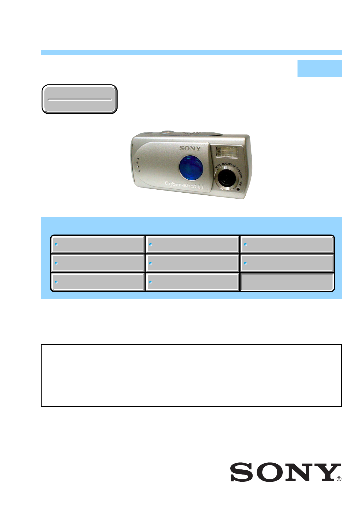
Photo: SILVER model
Link
Link
SPECIFICATIONS
SPECIFICATIONS
BLOCK DIAGRAMS
BLOCK DIAGRAMS
LEVEL 2
US Model
Canadian Model
AEP Model
UK Model
E Model
Hong Kong Model
Australian Model
Chinese Model
Korea model
Tourist Model
Japanese Model
PRINTED WIRING BOARDS
PRINTED WIRING BOARDS
SERVICE NOTE
SERVICE NOTE
DISASSEMBLY
DISASSEMBLY
•For ADJUSTMENTS (SECTION 6), refer to SERVICE MANUAL, ADJ (987626351.pdf).
•For INSTRUCTION MANUAL, refer to SERVICE MANUAL, LEVEL 1 (987626341.pdf).
• This service manual contains information for Japanese model as well.
• Reference No. search on printed wiring boards is available.
• HELP: Sheet attachment positions and procedures of processing the flexible boards/harnesses are shown.
On the DD-209, PD-174 and TY-20 boards
This service manual provides the information that is premised the circuit board replacement service and not intended repair
inside the DD-209, PD-174 and TY-20 boards.
Therefore, schematic diagram, printed wiring board, waveforms, mounted parts location and electrical parts list of the DD-209,
PD-174 and TY-20 boards are not shown.
The following pages are not shown.
Schematic diagram ........................... Pages 4-11 to 4-24
Printed wiring board.......................... Pages 4-39 to 4-44
Waveforms..........................................
FRAME SCHEMATIC DIAGRAMS
FRAME SCHEMATIC DIAGRAMS
SCHEMATIC DIAGRAMS
SCHEMATIC DIAGRAMS
Mounted parts location ......................
Electrical parts list............................ Pages 5-7, 5-8, 5-10,
Pages 4-58 and 4-59
REPAIR PARTS LIST
REPAIR PARTS LIST
Pages 4-61 and 4-62
5-12 to 5-14
DIGITAL STILL CAMERA
Page 2

DSC-U30
COVER
COVER
SPECIFICATIONS
xCamera
[System]
Image device
Total pixels number of camera
Effective pixels number of camera
Lens Single focal lens
Exposure control
Data formats
Recording media
Flash Recommended distance: 0.5 m to
6.72 mm (1/2.7 type) color CCD
Primary color filter
Approx. 2 112000 pixels
Approx. 2 020000 pixels
f = 5.0 mm
(7/32 inches) (35 mm camera
conversion: 33 mm (1 5/16 inches))
F2.8
Automatic, Scene Selection
(5 modes)
Still images: DCF compliant
(Exif Ver. 2.2 JPEG compliant),
DPOF compatible
Movies: MPEG1 compliant (without
audio)
“Memory Stick”
1.8 m (1 foot 7 3/4 inches to 5 feet
10 3/4 inches)
[Output connector]
USB jack mini-B
[LCD screen]
LCD panel used
Total number of dots
2.5 cm (1.0 type) TFT drive
64 460 (293×220) dots
[Power, general]
Used batteries
Power consumpti on (when shooting)
Operating temperatur e range
Storage temperature range
Dimensions
Mass Approx. 123 g (4.3 oz) (two
Exif Print Compatible
PRINT Image Matching II
AAA Nickel-Metal Hydride
batteries (2) 2.4 V
5 V (from USB cable)
1.35 W
0°C to +40°C (+32°F to +104°F)
–20°C to +60°C (–4°F to +140°F)
85 × 40.3 × 29.7 mm
(3 3/8 × 1 5/8 × 13/16 inches)
(W/H/D, protruding portions not
included)
batteries, “Memory Stick,” and neck
strap included)
Compatible
xBC-CS2A/CS2B Ni-MH
battery charger
Input rating
Output rating
Operating temperature ran ge
Storage temperature range
Dimensions
Mass Approx. 90 g (3 oz)
100 – 240 V AC, 50/60 Hz, 3 W
DC OUT AA: 1.4 V,
AAA: 1.4 V,
0°C to +40°C (+32°F to +104°F)
–20°C to +60°C (–4°F to +140°F)
Approx. 71 × 30 × 91 mm
(2 7/8 × 1 3/16 × 3 5/8 inches)
(W/H/D)
400 mA × 2
160 mA × 2
Accessories
•HR11/45: HR03 (Size AAA) Ni-MH batteries (2)
•Battery case (1)
• BC-CS2A/CS2B Ni-MH battery charger (1)
•Power cord (mains lead) (1)
•USB cable (1)
•Neck strap (1)
•“Memory Stick” (8MB) (1)
•CD-ROM (USB driver SPVD-010) (1)
•Operating instructions (1)
Design and specifications are subject to change
without notice.
— 2 —
Page 3

DSC-U30
SAFETY-RELATED COMPONENT WARNING!!
COMPONENTS IDENTIFIED BY MARK 0 OR DOTTED LINE WITH
MARK 0 ON THE SCHEMATIC DIAGRAMS AND IN THE PARTS
LIST ARE CRITICAL TO SAFE OPERATION. REPLACE THESE
COMPONENTS WITH SONY PARTS WHOSE PART NUMBERS
APPEAR AS SHOWN IN THIS MANUAL OR IN SUPPLEMENTS
PUBLISHED BY SONY .
SAFETY CHECK-OUT
After correcting the original service problem, perform the following
safety checks before releasing the set to the customer.
1. Check the area of your repair for unsoldered or poorly-soldered
connections. Check the entire board surface for solder splashes
and bridges.
2. Check the interboard wiring to ensure that no wires are
"pinched" or contact high-wattage resistors.
3. Look for unauthorized replacement parts, particularly
transistors, that were installed during a previous repair. Point
them out to the customer and recommend their replacement.
4. Look for parts which, through functioning, show obvious signs
of deterioration. Point them out to the customer and
recommend their replacement.
5. Check the B+ voltage to see it is at the values specified.
6. Flexible Circuit Board Repairing
•Keep the tempera ture of the soldering iron around 270˚C
during repairing.
• Do not touch the soldering iron on the same conductor of the
circuit board (within 3 times).
• Be careful not to apply force on the conductor when soldering
or unsoldering.
ATTENTION AU COMPOSANT AYANT RAPPORT
À LA SÉCURITÉ!
LES COMPOSANTS IDENTIFÉS P AR UNE MARQUE 0 SUR LES
DIAGRAMMES SCHÉMA TIQUES ET LA LISTE DES PIÈCES SONT
CRITIQUES POUR LA SÉCURITÉ DE FONCTIONNEMENT. NE
REMPLACER CES COMPOSANTS QUE PAR DES PIÈSES SONY
DONT LES NUMÉROS SONT DONNÉS DANS CE MANUEL OU
DANS LES SUPPÉMENTS PUBLIÉS PAR SONY.
Unleaded solder
Boards requiring use of unleaded solder are printed with the leadfree mark (LF) indicating the solder contains no lead.
(Caution: Some printed circuit boards may not come printed with
the lead free mark due to their particular size.)
: LEAD FREE MARK
Unleaded solder has the following characteristics.
• Unleaded solder melts at a temperature about 40°C higher than
ordinary solder.
Ordinary soldering irons can be used but the iron tip has to be
applied to the solder joint for a slightly longer time.
Soldering irons using a temperature regulator should be set to
about 350°C.
Caution: The printed pattern (copper foil) may peel away if the
heated tip is applied for too long, so be careful!
• Strong viscosity
Unleaded solder is more viscous (sticky, less prone to flow) than
ordinary solder so use caution not to let solder bridges occur such
as on IC pins, etc.
• Usable with ordinary solder
It is best to use only unleaded solder but unleaded solder may
also be added to ordinary solder.
— 3 —
Page 4

DSC-U30
TABLE OF CONTENTS
Section Title Page
1. SERVICE NOTE
1-1. Note for Repair ································································1-1
1-2. Discharging of the SL-59 Flexible Board’s
Charging Capacitor (C601) ·············································1-1
1-2-1.Preparing the Short Jig ····················································1-1
1-2-2.Discharging the Capacitor ···············································1-1
1-3. Description on Self-diagnosis Display ····························1-2
2. DISASSEMBLY
2-1. Cabinet (Front) Assembly ···············································2-3
2-2. OP-17 Flexible Board······················································2-3
2-3. Cabinet (Rear) Assembly················································· 2-4
2-4. PD-174 Board··································································2-4
2-5. Bottom Frame Assembly·················································2-5
2-6. Lens Block Assembly······················································2-5
2-7. SL-59 Flexible Board ······················································2-6
2-8. CCD Block Assembly ·····················································2-6
2-9. TY-20 Board ···································································· 2-7
2-10. Cabinet (Upper) Assembly ··············································2-7
2-11. US-7 Flexible Board ························································2-8
2-12. DD-209 Board ································································· 2-8
2-13. Circuit Boards Location ··················································2-9
3. BLOCK DIAGRAMS
3-1. Overall Block Diagram (1/2)··········································· 3-1
3-2. Overall Block Diagram (2/2)··········································· 3-3
3-3. Power Block Diagram (1/2)·············································3-5
3-4. Power Block Diagram (2/2)·············································3-7
4. PRINTED WIRING BOARDS AND
SCHEMATIC DIAGRAMS
4-1. Frame Schematic Diagram ··············································4-1
4-2. Schematic Diagrams························································4-5
CD-425 FLEXIBLE (1/2) (CCD IMAGER)···················4-7
CD-425 FLEXIBLE (2/2) (CAMERA MODULE)·········4-9
SL-59 FLEXIBLE
(CHARGING CAPACITOR, FLASH UNIT)···············4-25
ST-79 (FLASH DRIVE) ················································4-25
US-7 FLEXIBLE (USB CONNECTOR)······················4-27
OP-17 FLEXIBLE (LENS COVER DETECT) ············4-28
SW-376 FLEXIBLE
(CONTROL SWITCH, MS CONNECTOR) ················4-29
RS-85, FP-532, FP-533 FLEXIBLE ·····························4-31
4-3. Printed Wiring Boards ···················································4-35
CD-425 FLEXIBLE ······················································4-37
SL-59 FLEXIBLE ·························································4-45
ST-79 ·············································································4-47
US-7 FLEXIBLE···························································4-49
OP-17 FLEXIBLE·························································4-51
SW-376 FLEXIBLE······················································4-53
4-4. Waveforms·····································································4-57
4-5. Mounted Parts Location ················································4-60
5. REPAIR PARTS LIST
5-1. Exploded V iews ····························································5-2
5-1-1. Cabinet Section ····························································· 5-2
5-1-2. Cabinet (Upper) and Bottom Section····························5-3
5-1-3. Stroboscope and Lens Section ······································5-4
5-1-4. Battery Holder and LCD Section ··································5-5
5-2. Electrical Parts List·······················································5-6
— 4 —
Page 5
DSC-U30
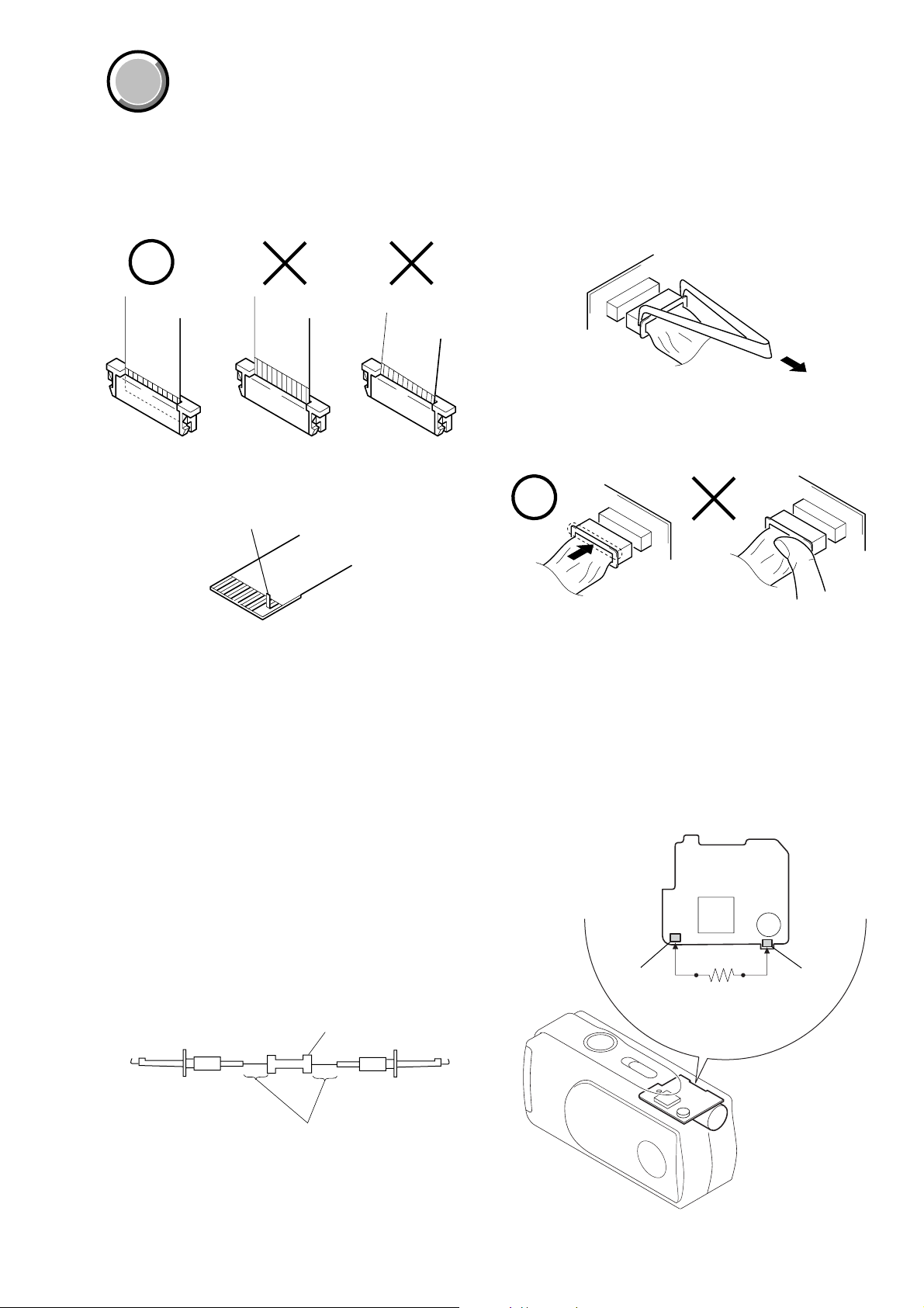
When installing a connector, don’t press down at wire of connector.
It is possible that a wire is snapped.
ST-79
R:1 kΩ/1 W
(Part code:
1-215-869-11)
A
B
COVER
COVER
SECTION 1
SERVICE NOTE
1-1. NOTE FOR REPAIR
Make sure that the flat cable and flexible board are not cracked of
bent at the terminal.
Do not insert the cable insufficiently nor crookedly.
Cut and remove the part of gilt
which comes off at the point.
(Be careful or some
pieces of gilt may be left inside)
When remove a connector, don’t pull at wire of connector.
It is possible that a wire is snapped.
1-2. DISCHARGING OF THE SL-59 FLEXIBLE BOARD’S CHARGING CAPACITOR
(C601)
The charging capacitor (C601) of the SL-59 flexible board is charged
up to the maximum 300 V potential.
There is a danger of electric shock by this high voltage when the
battery is handled by hand. The electric shock is caused by the
charged voltage which is kept without discharging when the main
power of the unit is simply turned off. Therefore, the remaining
voltage must be discharged as described below.
1-2-1. Preparing the Short Jig
To preparing the short jig, a small clip is attached to each end of a
resistor of 1 kΩ /1 W (1-215-869-11).
Wrap insulating tape fully around the leads of the resistor to prevent
electrical shock.
1 kΩ/1 W
Wrap insulating tape.
1-2-2. Discharging the Capacitor
Short-circuit between the A (positiv e) and the B (negativ e) terminals
on the ST-79 board with the short jig about 10 seconds.
1-1
Page 6

DSC-U30
1-3. DESCRIPTION ON SELF-DIAGNOSIS DISPLAY
Self-diagnosis display
• C: ss: ss
You can reverse the camera
malfunction yourself. (However,
contact your Sony dealer or local
authorized Sony service facility
when you cannot recover from the
camera malfunction.)
• E: ss: ss
Contact your Sony dealer or local
authorized Sony service facility.
Display Code
C:32:ss
C:13:ss
E:61:ss
E:91:ss
Countermeasure
Turn the power off and on again.
Format the “Memory stick”.
Insert a new “Memory Stick”.
Checking of lens drive circuit.
Checking of flash unit or replacement
of flash unit.
Cause
Trouble with hardware.
Unformatted memory stick is inserted.
Memory stick is broken.
When failed in the focus initialization.
Abnormality when flash is being
charged.
Caution Display During Error
SYSTEM ERROR
FORMAT ERROR
MEMORY STICK ERROR
—
1-2E
Page 7
DSC-U30
COVER
COVER
SECTION 2
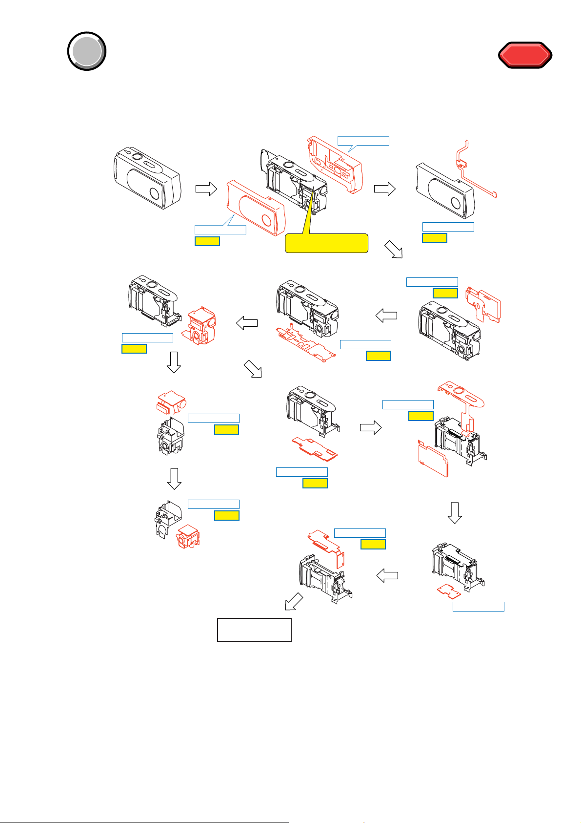
DISASSEMBLY
The following flow chart shows the disassembly procedure.
DISASSEMBLY
HELP
DISASSEMBLYDISASSEMBLY
Discharging the Capacitor
DISASSEMBLY
HELP
DISASSEMBLYDISASSEMBLY
HELP
HELP
HELP
DISASSEMBLY
HELP
DISASSEMBLYDISASSEMBLY
HELP
DISASSEMBLYDISASSEMBLY
HELP
DISASSEMBLYDISASSEMBLY
HELP
DISASSEMBLYDISASSEMBLY
HELP
DISASSEMBLYDISASSEMBLY
HELP
DISASSEMBLYDISASSEMBLY
HELP
DISASSEMBLYDISASSEMBLY
SERVICE POSITION
2-1
Page 8
DSC-U30
[SERVICE POSITION]
PC
USB cable
(1-823-932-11)
US-7 flexible board
PD-174 board
Cabinet (upper) block assembly
Cabinet (front) block assembly
BT holder assembly
TY-20 board
DD-209 board
Memory stick connector
LCD module
Lens block assembly
Insert the batteries*.
*: size AAA
Nickel Metal Hydride batteries (x2).
The procedure for a service position
1 2-1. CABINET (FRONT) ASSEMBLY ............................ (PAGE 2-3)
2 2-3. CABINET (REAR) ASSEMBLY............................... (PAGE 2-4)
3 2-4. PD-174 BOARD...................................................... (PAGE 2-4)
4 2-5. BOTTOM FRAME ASSEMBLY............................... (PAGE 2-5)
5 2-6. LENS BLOCK ASSEMBLY ..................................... (PAGE 2-5)
6 2-9. TY-20 BOARD ........................................................ (PAGE 2-7)
7 2-10. CABINET (UPPER) ASSEMBLY ............................ (PAGE 2-7)
8 2-11. US-7 BOARD.......................................................... (PAGE 2-8)
9 2-12. DD-209 BOARD ..................................................... (PAGE 2-8)
2-2
Page 9
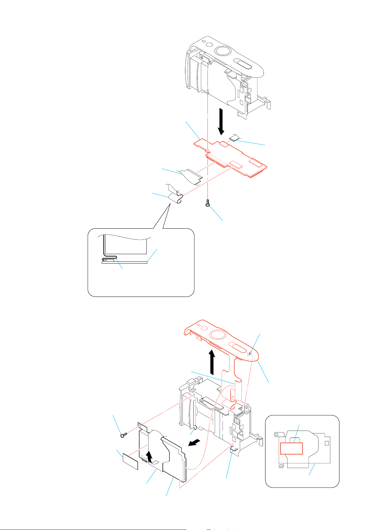
Note: Follow the disassembly procedure in the numerical order given.
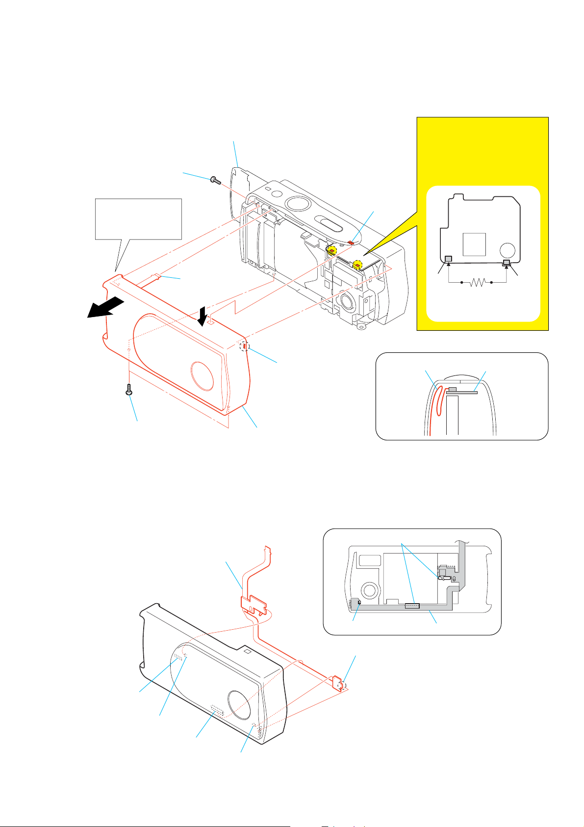
2-1. CABINET (FRONT) ASSEMBLY
DSC-U30
2 Screw (lock ace)
Note: Remove it while
taking care as
the flexible board
is connected.
7
1 Open battery lid.
8 Flexible board
(CN001)
4
6 Claw
Note: High-voltage cautions
Discharging the Capacitor
Short-circuit between the two
points of ST-79 flexible board
with the short jig about 10 seconds.
5 Claw
A
Processing the flexible board
OP-17 flexible board
ST-79
B
R:1 kΩ/1 W
(Part code:
1-215-869-11)
SW-376 board
3 Two screws (lock ace)
2-2. OP-17 FLEXIBLE BOARD
6 OP-17 flexible board
4 Boss
9 Cabinet (front) assembly
Processing the flexible board
(rear view)
claw
boss
OP-17 flexible board
1 Boss
5 Claw
3 Boss
2 Claw
2-3
Page 10
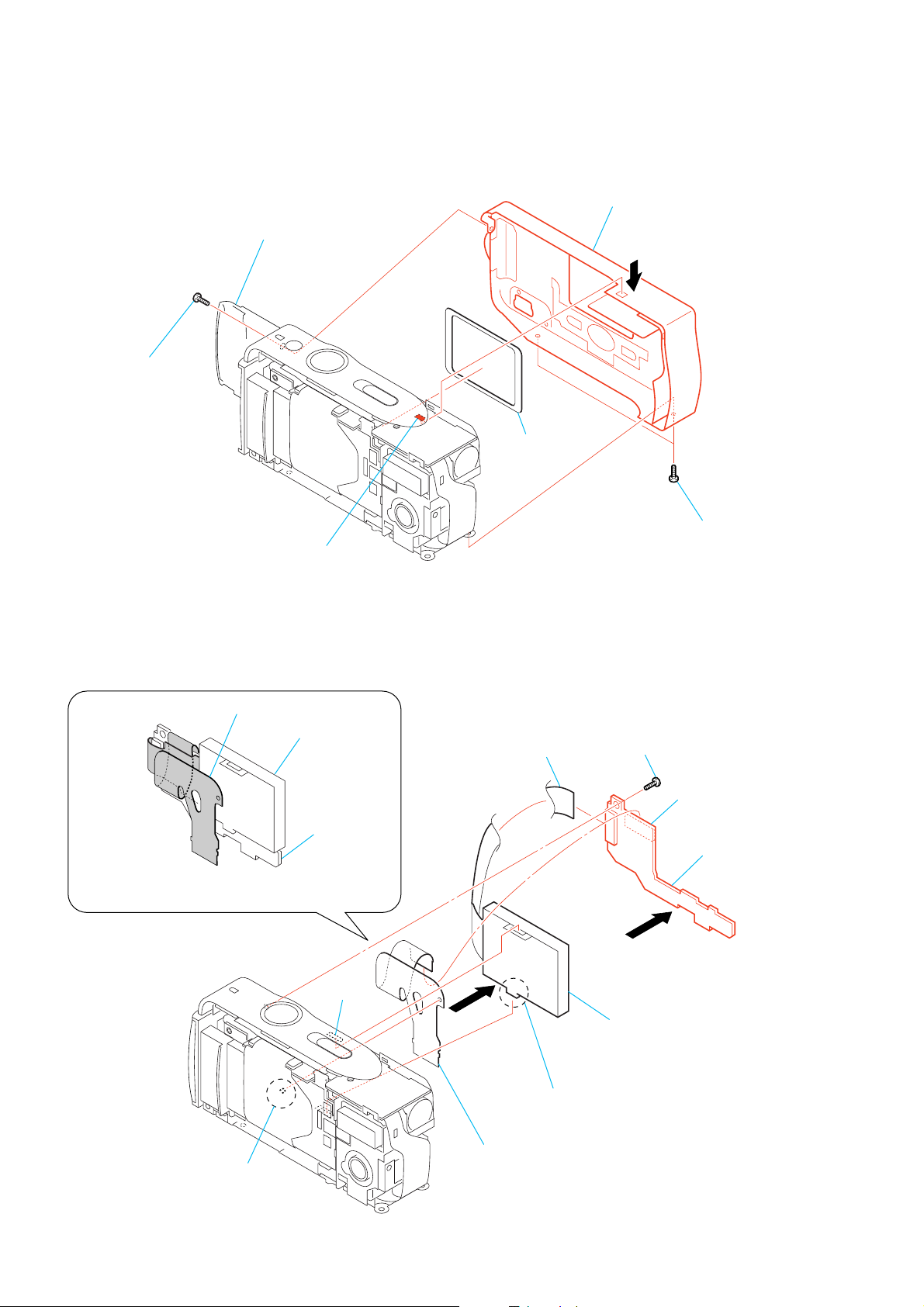
DSC-U30
2-3. CABINET (REAR) ASSEMBLY
1 Open battery lid.
2 Screw (lock ace)
6 Cabinet (rear) assembly
4
7 Cushion (LCD)
2-4. PD-174 BOARD
Processing the flexible board
Note: When installing FP-533 flexible board,
set it as shown in the figure.
5 Claw
FP-533 flexible board
LCD
PD-174 board
9 Flexible board (CN402)
3 Two screws (lock ace)
1 Screw (M1.7)
7 Connector (CN401)
qa PD-174 board
2
6 Boss
3 Claw
5
0 LCD
(ACX520AKM-1)
4 Boss
8 FP-533 flexible board (CN904)
2-4
Page 11
2-5. BOTTOM FRAME ASSEMBLY
7 Screw (M1.7)
5 Connector (CN903)
DSC-U30
Processing the flexible board
(bottom view)
Bottom frame assembly
Flexible board (SL-59)
9 Flexible board (CN908)
8
6 Screw (M1.7)
3 Boss
4 Cabinet (bottom) assembly
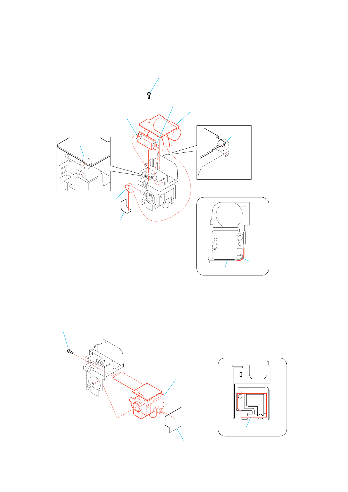
2-6. LENS BLOCK ASSEMBLY
Claw
1 Boss
Flexible board (SL-59)
0 Bottom frame assembly
2 Boss
2 Connector (CN002)
Lens block assembly
Note: When installing lens block assembly,
set it as shown in the figure.
Sheet attachment position
(bottom view)
Sheet (TY)
TY-20 board
6 Lens block assembly
4
3 Claw
5 Connector (CN902)
Sheet (USB)
1 Sheet (TY)
2-5
Page 12
DSC-U30
2-7. SL-59 FLEXIBLE BOARD
1 Screw (M1.7)
3 Claw
7 Flexible board
5 Claw
7 SL-59 flexible board
4 Claw
2 Claw
Sheet attachment position
6 Tape (K)
Tape (K)
SL-59 flexible board
2-8. CCD BLOCK ASSEMBLY
2 Screw (M1.7)
Sheet attachment position
3 CCD block assembly
Protection sheet (SL)
1 Protection sheet (SL)
2-6
Page 13
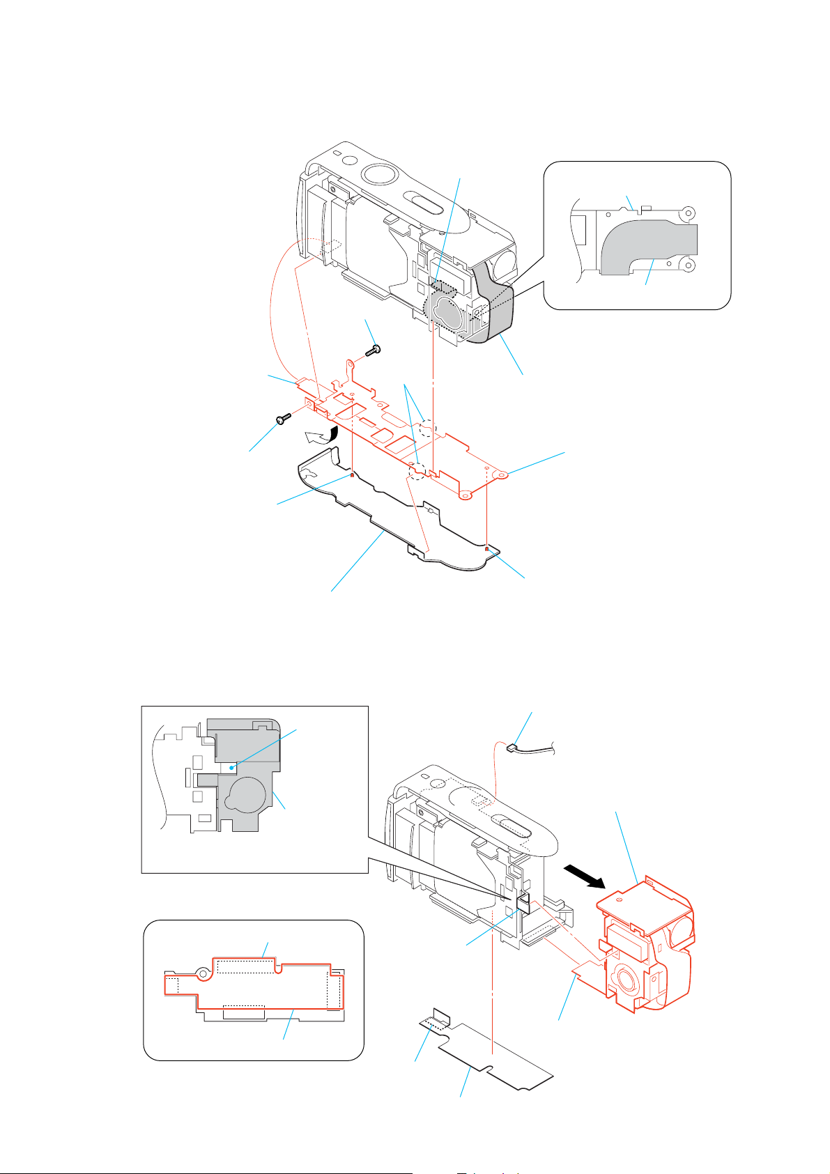
2-9. TY-20 BOARD
1 Flexible board (FP-532)
5 Flexible board (SW-376)
(CN906)
DSC-U30
6 TY-20 board
3
4 Flexible boards
(CN907)
(CN901)
Processing the flexible board
TY-20 board
Flexible board (SW-376)
Note: When installing Flexible board,
set it as shown in the figure.
2-10.CABINET (UPPER) ASSEMBLY
9 Connector
(memory stick connector)
2 Screw (M1.7)
7 Boss
8
qa Cabinet (upper) assembly
3 Screw (lock ace)
1 Sheet, lens
FP-533 flexible board
5 Claw
2
0 Memory stick connector
6
2-7
4 Claw
Sheet attachment position
Sheet, lens
Memory stick connector
Page 14
DSC-U30
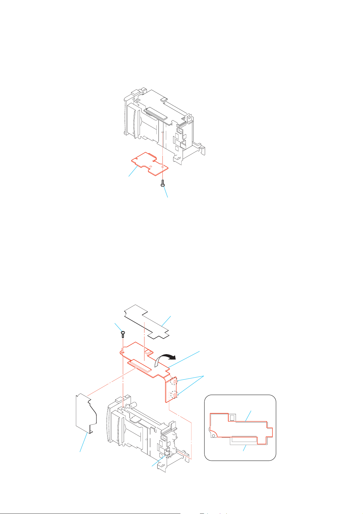
2-11.US-7 FLEXIBLE BOARD
2 US-7 flexible board
2-12.DD-209 BOARD
4 Screw (M1.7)
1 Screw (M1.7)
1 Insulating sheet (DD)
5
7 DD-209 board
3 Remove two solders.
2 FP-532 flexible board
Sheet attachment position
(bottom view)
Insulating sheet (DD)
DD-209 board
6 Claw
2-8
Page 15
2-13.CIRCUIT BOARDS LOCATION
DSC-U30
SW-376 FLEXIBLE
SL-59 FLEXIBLE
(Including ST-79)
CD-425 FLEXIBLE
OP-17 FLEXIBLE
PD-174
DD-209
US-7 FLEXIBLE
TY-20
Board Name Function
CD-425 FLEXIBLE CCD IMAGER, CAMERA MODULE
TY-20 CAMERA DSP, MAIN CPU, MEMORY, LENS DRIVE,
HI CONTROL
OP-17 FLEXIBLE LENS COVER DETECT
PD-174 LCD DRIVE, CONTROL SWITCH
DD-209 DC-IN, DC/DC CONVERTER
SL-59 FLEXIBLE CHARGING CAPACITOR, FLASH UNIT
(Including ST-79)
ST-79 FLASH DRIVE
US-7 FLEXIBLE USB CONNECTOR
SW-376 FLEXIBLE CONTROL SWITCH, MS CONNECTOR
2-9E
Page 16

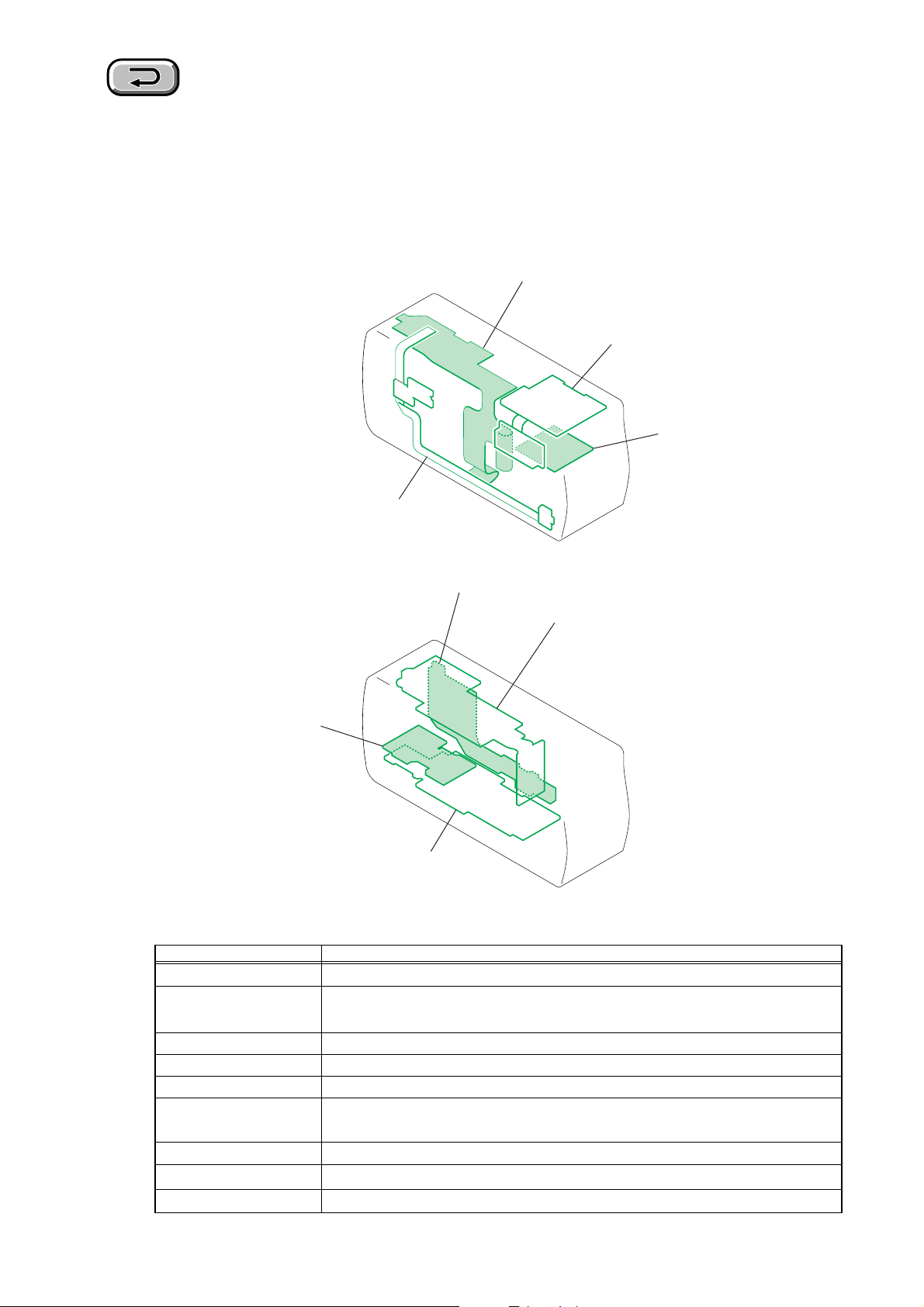
HELP
Sheet attachment positions and procedures of processing the flexible boards/harnesses are shown.
MAIN BLOCK SECTION
DSC-U30
2003.05.21 Update
OP-17 flexible board
Bottom frame assembly
Flexible board (SL-59)
SW-376 board
FP-533 flexible board
LCD
boss
claw
Sheet, lens
Memory stick connector
OP-17 flexible board
Sheet (TY)
Protection sheet (SL)
DD-209 board
PD-174 board
TY-20 board
Insulating sheet (DD)
DD-209 board
Tape (K)
Tape (K)
SL-59 flexible board
HELP
Page 17

COVER
COVER
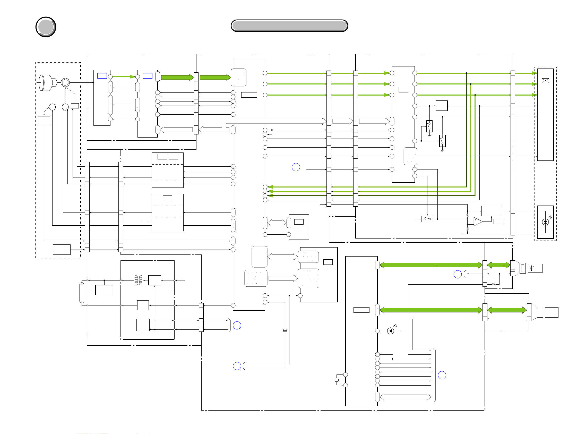
3. BLOCK DIAGRAMS
Link
Link
OVERALL BLOCK DIAGRAM (1/2) POWER BLOCK DIAGRAM (1/2)
OVERALL BLOCK DIAGRAM (1/2) POWER BLOCK DIAGRAM (1/2)
DSC-U30
OVERALL BLOCK DIAGRAM (2/2)
OVERALL BLOCK DIAGRAM (2/2)
POWER BLOCK DIAGRAM (2/2)
POWER BLOCK DIAGRAM (2/2)
Page 18
DSC-U30
COVER
COVER
SECTION 3
BLOCK DIAGRAMS
3-1. OVERALL BLOCK DIAGRAM (1/2)
CD-425 FLEXIBLE BOARD TY-20 BOARD (1/2)
10
12
16
17
V1, V2A, V2B,
1
V2C, V3A, V3B,
ı
4
6
ı
9
18
CCD OUT
RG, H1, H2
V3C, V4
VSHT
CN903
(1/2)
13
16
14
15
11
12
22
ı
25
17
21
IC101
4
CAMERA
1
MODULE
ı
3
5
ı
11
57
61
−
HALL+,
−
BIAS+,
−
DRIVE
+
DRIVE
FOCUS A, A, B, B
XFC RST SENS
LENS TEMP
(2/2)
H
IC302
CCD
IMAGER
(1/2)
SL-59 FLEXIBLE
BOARD
3
6
4
5
1
2
12
ı
15
7
11
ST-79 BOARD
CL601
CL531
ı
CL533
CL536,
537
T502
Q505 − 508
FLASH
DRIVE
Q504
FLASH
CHARGE
DETECT
XE A(H)
CHARGING
CAPACITOR
XE K (L)
05
ı
CL603
CL606,
607
LENS
FOCUS
MOTOR
FOCUS
SENSOR
LENS BLOCK
(SHUTTER)
IRIS
METER
M
LENS TEMP
SENSOR
IRIS
M
FLASH
UNIT
3. BLOCK DIAGRAMS
3. BLOCK DIAGRAMS
( ) : Number in parenthesis ( ) indicates the division number of schematic diagram where the component is located.
12
ı
CA AD00 − AD11
23
34
35
38
39
33
26
CAM SO, XCAM_SCK
27
IC202 IC206
(3/4)
HALL AMP,
HALL BIAS CONTROL,
HALL GAIN CONTROL
IRIS DRIVE
IC204
(3/4)
SHUTTER
DRIVE
FOCUS MOTOR
DRIVER
B+
SWITCH
CL501
CL507
CL526
CL516
CL508
Q501, 502
CA HD
CA FD
MCK
TG CLK
XCAM RESET
CL616
ı
ı
CL622
CL641
CL631
CL623
CN902
19
ı
CA AD00 − AD11
30
CA HD
8
CA FD
9
MCK
13
TG CLK
11
XCAM RESET
7
15
CAM SO, XCAM_SCK
16
HALL AD
HALL GAIN
HALL OFFSET
IRIS CONT1
CAM DD ON, MSHUT ON
PE EN0, PE DIR0A, PE DIR0B
ST UNREG
CN903 (2/2)
STRB ON
10
XSTB FULL
8
STB CHARGE
4
OVERALL (2/2)
(PAGE 3-4)
135 − 139
141 − 143
147 149
151 152
130
127
126
125
227
252
253
39
35
36
33
109
228
119
122
123
124
202
41
107
1
2
CAMERA DSP,
100
99
IC602 (1/2)
MAIN CPU
(1/4)
CAM SO, XCAM_SCK
18 19 50 51
53 − 55 57 − 59
61 − 63 65 − 67
70 71 73 74
261 − 263
265 − 267
270 − 275
277 − 279
281
98
88
167
86
87
218
44
45
46
47
242
243
245
213
27
OVERALL (2/2)
(PAGE 3-4)
XRST SYS
USB CLK EN
PANEL R
PANEL G
PANEL B
VR
VG
VB
VP
EEPROM TXD,
RXD, SCK
EEPROM RST
MC D00 − D15
MC A01 − A20
X601
48MHz
3
OVERALL (2/2)
(PAGE 3-4)
2
IC604
ı
4
EEPROM
(2/4)
6219
F3 F6 G3 − G7
H2 H3 H6 H7
J2 − J4 J6 J7
B2 B6 B7
C1 C2 C6 − C8
D1 − D3 D6 D7
E1 − E3 E6 E7
F1 F8
C4
CN904
XHD
XVD
TG CLK
XCS LCD
XRST SYS
D 1.5V
FP-533
FLEXIBLE
BOARD (1/2)
(1/2)
19
20
21
13
14
16
15
10
12
17 17
25
26
24
23
32 2
IC603
16M
FLASH ROM
(2/4)
X603
27MHz
163
162
PD-174 BOARD (1/2)
CN401
(1/2)
PANEL R
15
PANEL G
14
PANEL B
13
20
CAM SO, XCAM_SCK
21
XHD
18
XVD
19
TG CLK
24
XCS LCD
22
XRST SYS
VR
9
VG
8
VB
10
VP
11
FL+VO
IC602 (2/2)
CAMERA DSP,
MAIN CPU
(1/4)
22
23
255
258
259
257
134
90
26
30
31
166
214
247
50
23
51
19
45
48
67
47
78
20
D902
(MS ACCESS)
IC401
LCD
DRIVE
13
41 − 43
63 64
72 76 77
PANEL 2.8V
USB SUSPEND
VR
61
VG
7
VB
8
62
32
65
15
5
Q461
USB D
OVERALL (2/2)
(PAGE 3-4)
MS DIO, MS BS, MS SCLK
MS INT
USB JACK IN
SYS V
USB HOLD
USB VBUS
XMC NMI
XMC HELP
XCS MC
Q403 − 406
PSIG
DRIVE
Q402
5
Q401
FL−VO
4
USB JACK IN
OVERALL (2/2)
(PAGE 3-4)
CN402
RGT, HCK1, HCK2,
HST, WIDE, DWN,
EN, VCK, VST
Q462
BACKLIGHT
4
DRIVE
IC461
BACKLIGHT
CONTROL
1
3
US-7 FLEXIBLE
BOARD
CN907 CN050
5
USB D
6
USB 5V
2
3
1
SW-376 FLEXIBLE
CN906
BOARD (1/2)
(1/2)
15
18
MS DIO, MS BS, MS SCLK
20
MS INT
19 6
VCC
PANEL UNIT
R
7
G
8
B
6
PSIG
9
COM
26
5
10
11
15
16
22
ı
25
LED A
1
LED K
3
2
3
1
LCD901
COLOR
LCD
D901
BACKLIGHT
(USB)
(MS CONNECTOR)
2
4
8
MEMORY
STICK
249
ı
251
FR SI , FR SO, XFR SCK
3-1 3-2
A : VIDEO SIGNAL
Page 19

DSC-U30
COVER
COVER
3. BLOCK DIAGRAMS
3. BLOCK DIAGRAMS
3-2. OVERALL BLOCK DIAGRAM (2/2)
SW-376 FLEXIBLE
BOARD (2/2)
S001
PLAY STILL MOVIE
OP-17 FLEXIBLE BOARD
D102
(SELF TIMER)
S101
(LENS COVER OPEN)
S003
(SHUTTER)
S002
POWER
D001
(POWER )
CN001
1
3
XSELF TIMER LED
XLENS CAP OPEN
RS-85 FLEXIBLE BOARD
METAL DISC
RESET
XSHUTTER
XAE LOCK SW
MODE DIAL
XPOWER ON
XPOWER LED
TY-20 BOARD (2/2)
CN906 (2/2)
11
10
12
9
6
3
5
CN908
XRESET SW ON
1
( ) : Number in parenthesis ( ) indicates the division number of schematic diagram where the component is located.
34
46
77
74
6
9
32
65
33
61
80
36
26
23
ı
25
Q401
INVERTER
Q403
INVERTER
FR SI, FR SO, XFR SCK
Q402 (1/2)
LED
DRIVE
4
5
54
IC401
1
17
19
3
HI CONTROL
(4/4)
XSTB FULL
STB CHARGE
XRST SYS
XRST SYS
USB CLK EN
MS INT
USB JACK IN
SYS V
USB HOLD
USB SUSPEND
USB VBUS
XMC NMI
XMC HELP
XCS MC
OVERALL (1/2)
1
(PAGE 3-1)
OVERALL (1/2)
3
(PAGE 3-1)
OVERALL (1/2)
2
(PAGE 3-1)
OVERALL (1/2)
5
(PAGE 3-2)
PD-174 BOARD (2/2)
BT480
LITHIUM
BATTERY
D481
S480
MENU
S481
SCENE
S482
S483
EXEC
FP-533 FLEXIBLE
CN401 (2/2)
BOARD (2/2)
28
27 7
29
VL 3V
XCHARGE LED
KEY AD0
EVER 4.0V
CN904 (2/2)
6
5
7
INITIAL RESET,
BACK UP VCC
3
IC402
(4/4)
Q402 (2/2)
LED
DRIVE
5
4
8
6
EVER 3.0V
BACKUP VCC
10MHz
X403
32.768kHz
X401
DD-209 BOARD
FP-532 FLEXIBLE
79
73
31
14
53
62
63
16
55
29
28
51
52
20
ı
UNREG SO, UNREG SCK, XCS DDCON, SYS DD ON
22
76
Q404, 405
MODULATOR
OVERALL (1/2)
(PAGE 3-2)
BUZZER
4
BOARD
50
41
ı
44
48
49
CN001CN901
BUZZER
2
EVER 4.0V
PANEL 2.8V
CAM 15V
PANEL 13.5V
BUZZER 15V
CAM −7.5V
EVER 3.0V
8
ı
UNREG SO, UNREG SCK, XCS DDCON, SYS DD ON
11
USB 5VUSB 5V
3
4
D 1.5V
D 2.8V
A 2.8V
M 5V
FL −VO
IC001
DC/DC
CONTROL
(2/2)
44
ı
46
57
BATT UNREG
ACV UNREG
ST UNREG
CN002
+
–
BZ901
BUZZER
BT901
BATTERY
TERMINAL
1
05
3-3 3-4
Page 20

COVER
COVER
3. BLOCK DIAGRAMS
3. BLOCK DIAGRAMS
DSC-U30
3-3. POWER BLOCK DIAGRAM (1/2)
DD-209 BOARD (1/2)
CN001 (1/2)
USB 5V
3
4
Q001, 004, 018
(USB)
BT901
BATTERY
TERMINAL
+
–
US-7
FLEXIBLE
BOARD
CN050
VCC
1
2
3
F005
BATT UNREG/+
BATT GND/–
IC002
VOLTAGE DETECT
(1/2)
TY-20 BOARD
(1/2)
CN901 (1/2)
CN907
USB 5V
USB UNREG SW
FAST CHARGE
Vout 1Vin2
49
48
FP-532
FLEXIBLE
BOARD
(1/2)
Q002, 006
( ) : Number in parenthesis ( ) indicates the division number of schematic diagram where the component is located.
F004
D001
L018 L019
IC004
(1/2)
D008
DC/DC
CONVERTER
SWITCH
SWITCH
Q007
Q011
Q010
EMERGENCY
DETECT
Q003, 005
D002
Q008, 009
IC001
DC/DC CONTROL
(2/2)
OUT1p
VCC2
F001
F002
F003
D009 D005
36
37OUT1n
55VIN1–
41
L001
Q013, 016
SWITCHING
D004
L008 L010
Q015, 017
L002 L009
SWITCHING
L012
L013
L014
ST UNREG
ACV UNREG
BATT UNREG
DD CON SENS
EVER 4.0V
D 1.5V
D 2.8V
A 2.8V
PANEL 2.8V
A
POWER (2/2)
(PAGE 3-7)
EVER 3.0V
UNREG SO
UNREG SCK
XCS DDCON
SYS DD ON
56
VCC1
47 RST
48 LDON
45
DATA
46
CLK
44 XCS
57 CONT
RT
7
CT1
6
8 CT2
OUT4p
SCPIN
30
31OUT4n
53VIN4–
39OUT5n
38OUT5p
43OUT5S
52VIN5–
D012
42VCC3
20VCC5
29OUT6n
28OUT6p
18OUT6s
50VIN6–
19VCC4
23OUT9
1SCP9
80IN9–
22OUT10
4AMPIN
5AMPOUT
3IN10–
10
L007
L005
Q020, 022
SWITCHING
Q021, 023
SWITCHING
Q012
EMERGENCY
DETECT
Q024
Q025
Q014
SWITCHING
L003
Q019
SWITCHING
D006, 007
L015
13.5V/15V/–7.5V REG
7
3
1
VCC
VEE
STB
IC003
(1/2)
REG2
REG1
REG3
L017
BUZZER 15V
M 5V
Q026, 027
6
L016
8
4
CAM 15V
PANEL 13.5V
CAM –7.5V
FL –VO
CAM DD ON
B
POWER (2/2)
(PAGE 3-7)
05
3-5 3-6
Page 21

DSC-U30
COVER
COVER
3. BLOCK DIAGRAMS
3. BLOCK DIAGRAMS
3-4. POWER BLOCK DIAGRAM (2/2)
TY-20 BOARD (2/2)DD-209 BOARD (2/2)
CN901 (2/2)
3
ST UNREG
ı
1
M 5V
17
16
CAM DD ON
15
BUZZER 15V
51
D 2.8V
19
18
CAM 15V
7
6
CAM –7.5V
9
8
A 2.8V A 2.8V
14
13
B
POWER (1/2)
(PAGE 3-6)
CN001 (2/2)
ST UNREG
M 5V
CAM DD ON
BUZZER 15V
D2.8V
CAM 15V
CAM –7.5V
A 2.8V
FP-532 FLEXIBLE
BOARD (2/2)
49
ı
51
35
36
37
1
33
34
45
46
43
44
38
39
( ) : Number in parenthesis ( ) indicates the division number of schematic diagram where the component is located.
SL-59 FLEXIBLE BOARD
BUZZER 15V
(MS ACCESS)
IC605
USB 1.5V REG
(2/4)
2
VIN
IC606
USB 3.1V REG
(2/4)
2
VIN
5
CE
D902
VOUT
VOUT
L202
FB202
D 2.8V
MS PWR ON
228
107
234
IC206
IRIS DRIVE,
HALL AMP
(3/4)
Q901
CAM DD ON
IC202
IRIS DRIVE,
HALL BIAS/GAIN
CONTROL
(3/4)
L201
D 2.8V
FB602
FB603
3
L604
L602
USB 1.5V
3
USB 3.1V
L601
L605
IC603
16M FLASH ROM
(2/4)
IC604
EEPROM
(2/4)
IC602
CAMERA DSP,
MAIN CPU
(1/4)
CAM DD ON
STRB ON
MS PWR ON
IC204
SHUTTER DRIVE,
FOCUS DRIVE
(3/4)
ST UNREG
STB CHARGE
XSTB FULL
Q201
F SENS VCC
L903
L902
L904
Q902
CAM –7.5V
FB902
D901
ST UNREG
CN903
1
ı
3
M 5V
9
STRB ON STRB ON
CN902
CAM 15V
FE3V
DRV3V
TG3V
CL636, 637 CL521, 522
10
4
8
18
CD-425 FLEXIBLE BOARD
2
3
4
5
6
CL501
CL616
ı
CL507
CL622
CL641 CL526
CL623 CL508
CL631 CL516
SW-376 FLEXIBLE BOARD OP-17 FLEXIBLE BOARD
CN906 CN001
D 2.8V
4
D 2.8V
7
MS VCC
21
22
ST-79 BOARD
L501
ı
M 5V
IC101
CAMERA
MODULE
(2/2)
D 2.8V
D001
(POWER)
VCC
Q501, 502
2
(MS CONNECTOR)
9
Q505 - 507
FLASH
DRIVE
L301
FB301
Q503
TRANS
DRIVE
MEMORY
STICK
STB CHARGE
XSTB FULL
IC302
CCD IMAGER
(1/2)
D102
(SELF TIMER)
2
1
3
4
T502
PS
F
C601
CHARGING
D502
5
Q508
Q504
CL531
CL533
CL536, 537
F SENS VCC
CAPACITOR
XE A(H)
CL601
ı
ı
CL603
+
XE K(L)
CL606, 607
LENS BLOCK
8
FOCUS
SENSOR
FLASH
UNIT
POWER (1/2)
(PAGE 3-5)
05
40
D 1.5V
ı
42
FL –VO
EVER 4.0V
UNREG SO
EVER 3.0V
28
29
30
31
32
13
14
15
16
17
10
9
11
8
6
7
12
PANEL 13.5V
PANEL 2.8V
DD CON SENS
BATT UNREG
ACV UNREG
UNREG SCK
XCS DDCON
SYS DD ON
A
FAST CHARGE
USB UNREG SW
12
D 1.5V
ı
10
FL –VO
24
PANEL 13.5V
23
22
PANEL 2.8V
21
20
EVER 4.0V
39
38
DD CON SENS
37
BATT UNREG
36
ACV UNREG
35
UNREG SO
42
UNREG SCK
43
XCS DDCON
41
SYS DD ON
44
FAST CHARGE
46
USB UNREG SW
45
EVER 3.0V
40
66 DD CON SENS
BATT SENS
67
68 ACV SENS
20 UNREG SO
21 UNREG SCK
22 XCS DDCON
76 SYS DD ON
48
72 USB UNREG SW
USB PWR ON
FAST CHARGE
STB CHG
XSTB FULL
IC401
HI CONTROL
(4/4)
78
STB CHARGE
46
34
BackUp Vcc
XSTB FULL
D 1.5V
EVER 4.0V
3.3V REG
2
VIN
4
CE
INITIAL RESET, BACK UP VCC
L401
6
VOUT
8
VRO
IC403
(4/4)
IC402
(4/4)
VOUT
VIN
VBAT
FP-533 FLEXIBLE
BOARD
CN904
32
33
3
D402
7
3
30
29
28
27
6
D 2.8V
FL +VO
FL –VO
PANEL 13.5V
PANEL 2.8V
VL 3V
268
28
2
1
4
5
6
7
CN401
L401
LITHIUM
BATTERY
BT480
D481
IC461
BACKLIGHT
CONTROL
POFF E3
IC401
LCD DRIVER
4
Q408, 409
59
Q462
BACKLIGHT
DRIVE
Q410
REF VOLTAGE
GEN.
D402
CN402
LED A
1
LED K
3
CRext
12
REF
14
VDDG
19
VDD
21
PANEL UNIT
D901
BACKLIGHT
LCD901
COLOR
LCD
PD-174 BOARD
3-7 3-8 E
Page 22

COVER
COVER
PRINTED WIRING BOARDS AND SCHEMATIC DIAGRAMS
4-1. FRAME SCHEMATIC DIAGRAM
SECTION 4
4-2. SCHEMATIC DIAGRAMS 4-3. PRINTED WIRING BOARDS
4-2. SCHEMATIC DIAGRAMS 4-3. PRINTED WIRING BOARDS
DSC-U30
FRAME SCHEMATIC DIAGRAM
A
B
C
D
E
F
BZ901
BUZZER
TERMINAL
BT901
BATTERY
5
CN002
1 BUZZER
2 GND
76
2P
81410
DD-209 BOARD PD-174 BOARD
51P
CN001
BUZZER_15V2BUZZER3USB_5V4USB_5V5REG_GND6FAST_CHARGE7USB_UNREG_SW8SYS_DD_ON9UNREG_SCK10UNREG_SO11XCS_DDCON12EVER_3.0V13EVER_4.0V14EVER_4.0V15DD_CON_SENS16BATT_UNREG17ACV_UNREG18REG_GND19REG_GND20REG_GND21REG_GND22REG_GND23REG_GND24REG_GND25REG_GND26REG_GND27REG_GND28FL_-VO29PANEL_13.5V30PANEL_13.5V31PANEL_2.8V32PANEL_2.8V33D_2.8V34D_2.8V35M_5V36M_5V37CAM_DD_ON38A_2.8V39A_2.8V40D_1.5V41D_1.5V42D_1.5V43CAM_-7.5V44CAM_-7.5V45CAM_15V46CAM_15V47REG_GND48REG_GND49ST_UNREG50ST_UNREG51ST_UNREG
1
FP-532 FLEXIBLE BOARD FP-533 FLEXIBLE BOARD
4
6
8
10
13
15
16
18
20
21
22
23
24
25
M_5V17M_5V
A_2.8V14A_2.8V
PANEL_2.8V
PANEL_13.5V
PANEL_2.8V
D_2.8V19D_2.8V
CAM_DD_ON
FL_-VO
REG_GND26REG_GND27REG_GND28REG_GND29REG_GND30REG_GND31REG_GND32REG_GND33REG_GND34REG_GND
PANEL_13.5V
D_1.5V11D_1.5V12D_1.5V
CAM_15V7CAM_15V
REG_GND5REG_GND
CAM_-7.5V9CAM_-7.5V
51P
CN901
50
51
BUZZER
BUZZER_15V
35
36
37
38
41
42
43
44
45
46
47
48
USB_5V49USB_5V
REG_GND
FAST_CHARGE
USB_UNREG_SW
UNREG_SCK
SYS_DD_ON
UNREG_SO
XCS_DDCON
EVER_4.0V39EVER_4.0V40EVER_3.0V
BATT_UNREG
DD_CON_SENS
ACV_UNREG
12
29P
CN401
1
33P
ST_UNREG2ST_UNREG3ST_UNREG
CN904
139
FL_-VO2FL_+VO3REG_GND4PANEL_13.5V5PANEL_13.5V6PANEL_2.8V7PANEL_2.8V8VG9VR10VB11VP12REG_GND13PANEL_B14PANEL_G15PANEL_R16REG_GND17XRST_SYS18XHD19XVD20LCD_SO21XLCD_SCK22XCS_LCD23REG_GND24TG_CLK25REG_GND26D_2.8V27XCHARGE_LED28VL_3V29KEY_AD0
1
14
15
16
17
18
19
21
22
PANEL_2.8V
23VP24VB25VR26VG27
XVD
XHD
REG_GND
PANEL_B
LCD_SO
PANEL_R20PANEL_G
REG_GND
XRST_SYS
33
FL_-VO
32
FL_+VO
31
REG_GND
29
30
PANEL_13.5V
PANEL_13.5V
28
PANEL_2.8V
13
XLCD_SCK
12
XCS_LCD
11
REG_GND
10
TG_CLK
9
REG_GND
8
D_2.8V
6
7
VL_3V
XCHARGE_LED
16
4
5
KEY_AD0
MODE_DIAL (N.C.)
1
2
3
XPOWER_ON (N.C.)
XPOWER_LED (N.C.)
XRESET_SW_ON (N.C.)
LED_A
LED_K
174
27PCN402
1
N.C.
2
3
TEST2
4
RGT
5
B
6
R
7
G
8
PSIG
9
HCK1
10
HCK2
11
CRext
12
DSUT
13
REF
14
HST
15
WIDE
16
CS
17
VSSG
18
VDDG
19
VSS
20
VDD
21
DWN
22
EN
23
VCK
24
VST
25
COM
26
TEST
27
183 15 19 201 112
PANEL UNIT
LCD901
1inch
COLOR LCD
D901
LED BACKLIGHT
31PCN902
CD_GND
1
CAM_15V
G
H
IC101
CAMERA MODULE
I
(CH-124 BOARD) BOARD
CD-425
FLEXIBLE
J
K
L
M
CCD
LENS
N
2
CAM_-7.5V
3
FE3V
4
DRV3V
5
TG3V
6
XCAM_RESET
7
CA_HD
8
CA_FD
9
CD_GND
10
TG_CLK
11
CD_GND
12
MCK
13
CD_GND
14
XCAM_SCK
15
CAM_SO
16
XCAM_CS
17
XTG_CS
18
CA_AD0
19
CA_AD4
20
CA_AD8
21
CA_AD1
22
CA_AD5
23
CA_AD9
24
CA_AD2
25
CA_AD6
26
CA_AD10
27
CA_AD3
28
CA_AD7
29
CA_AD11
30
CD_GND
31
XFC_RST_SENS
F_SENS_VCC
F_SENS_GND
LENS TEMP
FOCUS_B
FOCUS_A
FOCUS_B
FOCUS_A
DRIVE-
DRIVE+
HALL-
BIAS+
HALL+
23PCN906
XAE_LOCK_LED (N.C.)
XTALLY_LED (N.C.)
XSELF_TIMER_LED
CN050
XLENS_CAP_OPEN
5P
TY-20 BOARD
25PCN903
ST_UNREG2ST_UNREG3ST_UNREG4STB_CHARGE5REG_GND6REG_GND7REG_GND8XSTB_FULL9M_5V10STRB_ON11DRIVE-12DRIVE+13HALL-14BIAS+15BIAS-16HALL+17XFC_RST_SENS18F_SENS_VCC19F_SENS_GND20N.C.21LENS_TEMP22FOCUS_B23FOCUS_A
1
15P
1
2
3
4
BIAS-
5
6
7
SL-59
8
FLEXIBLE
9
N.C.
10
BOARD
11
12
13
14
15
ST-79
BOARD
FLASH UNIT
FOCUS_B25FOCUS_A
24
C601
CHARGING
CAPACITOR
6PCN908
XRESET_SW_ON2REG_GND3XCPC_IN (N.C.)4EVER_4.0V (N.C.)5LANC_IN (N.C.)6LANC_OUT (N.C.)
1
RS-85
FLEXIBLE
BOARD
8PCN907
USB_JACK_IN2USB_5V3USB_5V4REG_GND (N.C.)5USB_D+6USB_D-7USB_GND8USB_GND
1
US-7
FLEXIBLE BOARD
XPOWER_LED
XPOWER_ON
XAE_LOCK_SW
XSHUTTER
MODE_DIAL
MS_VSS
MS_VCC (N.C.)
MS_VCC (N.C.)
MS_DIO
MS_INT
MS_SCLK
MS_VCC
MS_VCC
MS_VSS
1VCC
2D-
3D+
4ID
5GND
D_2.8V
D_2.8V
MS_BS
1
2
3
4
5
6
7
GND
8
9
10
11
12
GND
13
14
15
16
17
18
19
20
21
22
23
SW-376
FLEXIBLE
(USB)
BOARD
CN001
XSELF_TIMER_LED
XLENS_CAP_OPEN
STATIC_GND
D_2.8V
6P
1
2
3
GND
4
5
N.C.
6
MS CONNECTOR
10P
VSS
1
BS
2
VCC (N.C.)
3
DIO4
5
N.C
6
INT
7
N.C
SCLK
8
VCC
9
VSS
10
OP-17
FLEXIBLE
BOARD
10
MEMORY
STICK
MEMORY STICK
1
05
4-1 4-2
FRAME
Page 23

4-2. SCHEMATIC DIAGRAMS
COVER
COVER
4-2. SCHEMATIC DIAGRAMS
4-2. SCHEMATIC DIAGRAMS
THIS NOTE IS COMMON FOR SCHEMATIC DIAGRAMS
(In addition to this, the necessary note is printed in each block)
DSC-U30
(For schematic diagrams)
• All capacitors are in µF unless otherwise noted. pF : µ
Link
µF. 50 V or less are not indicated e xcept for electrolytics
and tantalums.
• Chip resistors are 1/10 W unless otherwise noted.
kΩ=1000 Ω, MΩ=1000 kΩ.
• Caution when replacing chip parts.
New parts must be attached after removal of chip.
Be careful not to heat the minus side of tantalum
capacitor, Because it is damaged by the heat.
• Some chip part will be indicated as follows.
Example C541 L452
22U 10UH
TA A 2520
Kinds of capacitor
Case Size
External dimensions (mm)
• Constants of resistors, capacitors, ICs and etc with XX
indicate that they are not used.
In such cases, the unused circuits may be indicated.
•Parts with ★ differ according to the model/destination.
Refer to the mount table for each function.
• All variable and adjustable resistors have characteristic
curve B, unless otherwise noted.
• Signal name
XEDIT→ EDIT PB/XREC → PB/REC
• 2: non flammable resistor
• 5: fusible resistor
• C: panel designation
• A: B+ Line
• B: B– Line
• J : IN/OUT direction of (+,–) B LINE.
• C: adjustment for repair.
• A: VIDEO SIGNAL (ANALOG)
• A: AUDIO SIGNAL (ANALOG)
• A: VIDEO/AUDIO SIGNAL
• A: VIDEO/AUDIO/SERVO SIGNAL
• A: SERVO SIGNAL
• Circled numbers refer to waveforms.
(Measuring conditions voltage and waveform)
•Voltages and waveforms are measured between the
measurement points and ground when camera shoots
color bar chart of pattern box. They are reference values
and reference waveforms.
(VOM of DC 10 MΩ input impedance is used)
•Voltage values change depending upon input
impedance of VOM used.)
1. Connection
Pattern box
L
Front of the lens
L = About 30 cm
2. Adjust the distance so that the display of Fig. a can be
obtain.
C
C=D
D
AB B
Fig.a (Picture on LCD display)
When indicating parts by reference number, please
include the board name.
A=B
A
Note : The components identified by mark 0 or
dotted line with mark 0 are critical for safety.
Replace only with part number specified.
Note : Les composants identifiés par une marque
0 sont critiques pour la sécurité.
Ne les remplacer que par une pièce portant
le numéro spécifie.
4-5
Page 24

COVER
COVER
4-2. SCHEMATIC DIAGRAMS
Link
Link
CD-425 FLEXIBLE BOARD (1/2)
CD-425 FLEXIBLE BOARD (1/2)
(CCD IMAGER)
(CCD IMAGER)
US-7 FLEXIBLE BOARD
US-7 FLEXIBLE BOARD
DSC-U30
(USB CONNECTOR)
(USB CONNECTOR)
CD-425 FLEXIBLE BOARD (2/2)
CD-425 FLEXIBLE BOARD (2/2)
(CAMERA MODULE)
(CAMERA MODULE)
SL-59 FLEXIBLE BOARD
SL-59 FLEXIBLE BOARD
(CHARGING CAPACITOR, FLASH UNIT)
(CHARGING CAPACITOR, FLASH UNIT)
ST-79 BOARD
ST-79 BOARD
COMMON NOTE FOR SCHEMATIC DIAGRAMS WAVEFORMS
COMMON NOTE FOR SCHEMATIC DIAGRAMS WAVEFORMS
(FLASH DRIVE)
(FLASH DRIVE)
OP-17 FLEXIBLE BOARD
OP-17 FLEXIBLE BOARD
(LENS COVER DETECT)
(LENS COVER DETECT)
SW-376 FLEXIBLE BOARD
SW-376 FLEXIBLE BOARD
(CONTROL SWITCH, MS CONNECTOR)
(CONTROL SWITCH, MS CONNECTOR)
RS-85, FP-532, FP-533 FLEXIBLE BOARD
RS-85, FP-532, FP-533 FLEXIBLE BOARD
Page 25

COVER
COVER
For Schematic Diagram
• Refer to page 4-37 for printed wiring board.
• Refer to page 4-57 for waveform.
4-2. SCHEMATIC DIAGRAMS CD-425 FLEXIBLE BOARD
4-2. SCHEMATIC DIAGRAMS CD-425 FLEXIBLE BOARD
DSC-U30
1
32
4
56
7
8
9
CD-425 FLEXIBLE BOARD (1/2)
A
B
C
D
CCD IMAGER(CCD1 BLOCK)
XX MARK:NO MOUNT
NO MARK:REC/PB MODE
R:REC MODE
P:PB MODE
1
(2/2)
V3B
CAM_-7.5V
V3C
V2C
V3A
V2B
V2AV4V1
VSHT
GND
H1RGH2
GND
CCD_OUT
GND
CAM_15V
GND
L301
100uH
1
3
1
6
Q302
2SC4250(T5LSONY1)
BUFFER
R311
R11.8/P0
C311
0
XX
CH
R308
5.6k
R15.1/P0
R11.1/P0
C312
CH
C309
0.1u
16V
XX
V42V3A
Note:The voltage and
waveform of IC302
cannot be measured,
because it is mounted
by the side of lens.
V3B4V3C5VHOLD
E
D301
MA111-(K8).S0
R303
0
R304
0
0
C314
R302
C305
0.22u
R301
C313
100k
0.01u
10u
F
C301
0.22u
25V
FB301
HS601
C302
C315
1.5u
G
SIGNAL PATH
VIDEO
SIGNAL
1.5u
35V
35V
C303
10u
Y/CHROMA
REC
25V
R306
φ SUB
18
0
C307
2200p
IC302
CCD IMAGER
IC302
ICX454JQF-13
GND15VL16H117H2
14
V2A7V2B8V2C9V1
VDD
GND
10
11
12RG13
C306
0.1u
16V
R307
3.9k
VOUT
C310
0.1u
16V
Precautions for Replacement of CCD Imager
•The CD-425 flexible board mounted as a repair part is not
equipped with a CCD imager.
When replacing this board, remove the CCD imager from the
old one and mount it onto the new one.
• If the CCD imager has been replaced, carry out all the
adjustments for the camera section.
• As the CCD imager may be damaged by static electricity from
H
its structure, handle it carefully like for the MOS IC.
In addition, ensure that the receiver is not covered with dusts
nor exposed to strong light.
05
4-7 4-8
CD-425 (1/2)
Page 26

DSC-U30
COVER
COVER
For Schematic Diagram
• Refer to page 4-37 for printed wiring board.
4-2. SCHEMATIC DIAGRAMS CD-425 FLEXIBLE BOARD
4-2. SCHEMATIC DIAGRAMS CD-425 FLEXIBLE BOARD
1
2
5 12
89674
10
113
:Voltage measurment of the CSP ICs
CD-425 FLEXIBLE BOARD(2/2)
A
B
C
D
E
F
CAMERA MODULE(CH BLOCK)
TY-20
(2/4)
CN902
(PAGE 4-14)
LND101
31
LND102
LND103
LND104
LND105
LND106
LND107
LND108
LND109
LND110
LND111
LND112
LND113
LND114
LND115
LND116
LND117
LND118
LND119
LNC120
LND121
LND122
LND123
LND124
LND125
LND126
LND127
LND128
LND129
LND130
1
LND131
CD_GND
CA_AD11
CA_AD7
CA_AD3
CA_AD10
CA_AD6
CA_AD2
CA_AD9
CA_AD5
CA_AD1
CA_AD8
CA_AD4
CA_AD0
XTG_CS
XCAM_CS
CAM_SO
XCAM_SCK
CD_GND
MCK
CD_GND
TG_CLK
CD_GND
CA_FD
CA_HD
XCAM_RESET
TG3V
DRV3V
FE3V
CAM_-7.5V
CAM_15V
CD_GND
TG3V
DRV3V
FE3V
D11
D10
D7
D3
D6
D2
D9
D5
D1
D8
D4
D0
XCAM_SO
26
XCAM_SCK
27
D1
28
D0
29
GND
30
CLPOB
31
CLPDM
32
XCAM_RESET
33
CA_HD
34
CA_FD
35
GND
36
GND
37
MCK
38
TG_CLK
39
HVDD
40
GND
41
CAM_-7.5V
42
CAM_15V
TG3V
FE3V
DRV3V
43
TG3V
44
WEN
45
FE3V
46
DRV3V
47
GND
48
GND
49
GND
50
and the Transistors with mark,are
not possible.
D6
D7
D8
D9
D10
D11
24
25
D1021D1122D1223D13
XTG_CS
XGCAM_CS
D5
D3
D4
IC101
CAMERA MODULE
(CH-124 BOARD)
D0
D1
D2
IC101
V3C
V3B
V3A
V2A
10V411
12D213D314D415D516D617D718D819D920
VSHT
V2BV4V2C
5
7V28
V3A9V3B
V1A6V1B
RG
3RG4
CCD_OUT
H2
H1
CCD_OUT
1
H12H2
CAM_-7.5V
V3C
V2C
V4
V3A
V3B
V1
V2A
V2B
VSHT
GND
RG
H1
H2
GND
CCD_OUT
GND
CAM_15V
GND
1
(1/2)
DRV3V
(XCAM_SO)
(D13)
GND
GND
(D1)
(D5)
(D9)
GND
GND
GND
GND
V3C
V2C
V4
V3A
V3B
V1
95
93 94
RG
H1
H2
85 86 87 88 89 90 91 92
84
83
82
81
80
79
78
77
76
V2A
V2B
VSHT
G
H
05
CD-425 (2/2)
SIGNAL PATH
REC
VIDEO
SIGNAL
Y/CHROMA
GND52GND53GND54GND55GND56GND57V158GND59GND60GND61SUB62GND63GND64GND65GND66GND67GND68GND69GND70GND71GND72GND73GND74GND75GND
51
VSHT
V1
4-9 4-10
Page 27

Schematic diagrams of the TY-20, PD-174 and DD-209 boards are not shown.
Pages from 4-11 to 4-24 are not shown.
Page 28

DSC-U30
COVER
COVER
For Schematic Diagram
• Refer to page 4-45 for printed wiring board. (SL-59 FLEXIBLE BOARD)
• Refer to page 4-47 for printed wiring board. (ST-79 BOARD)
3 151 112
SL-59 FLEXIBLE BOARD
A
CHARGING CAPACITOR,FLASH UNIT
4
(Including ST-79 board)
B
CL622
CL621
CL620
C
D
LND601
ST_UNREG
1
E
F
TY-20 (3/4)
CN903
G
(PAGE4-15)
H
I
05
25
LND602
ST-UNREG
LND603
ST_UNREG
LND604
STB_CHARGE
LND605
REG_GND
LND606
REG_GND
LND607
REG_GND
LND608
XSTB_FULL
LND609
M_5V
LND610
STRB_ON
LND611
DRIVE- DRIVE-
LND612
DRIVE+
LND613
HALL-
LND614
BIAS+
LND615
BIAS-
LND616
HALL+
LND617
XFC_RST_SENS
LND618
LND619
F_SENS_GND F_SENS_GND
LND620
NC
LND621
LENS_TEMP
LND622
FOCUS_B
LND623
FOCUS_A
LND624
FOCUS_B
LND625
FOCUS_A
CL619
CL618
CL617
CL616
CL623
CL658
CL657
CL656
CL655
CL654
CL630
CL629
CL628
CL627
CL626
CL631
CL637
CL636
CL641
4-2. SCHEMATIC DIAGRAMS
4-2. SCHEMATIC DIAGRAMS
5
ST-79 BOARD
FLASH DRIVE(ST BLOCK)
XX MARK:NO MOUNT
Q502
MCH3306-TL
B+ SWITCH
L501
10uH
CL507
CL506
CL501
CL502
CL503
CL505
CL504
CL508
CL554
CL556
CL555
CL558
CL557
CL514
CL513
CL512
CL511
CL516
CL521
CL522
CL526
R501
4700
R502
100k
Q501
DTC144EHT2L
SWITCHING
0
2.4
R503
10k
0.3
2.4
C503
2.4
CL559
SL-59 FLEXIBLE BOARD ST-79 BOARD
SL-59 FLEXIBLE BOARD ST-79 BOARD
76
81410
12
139
NO MARK:REC/PB MODE
R:REC MODE
P:PB MODE
C504
10u
10u
0.3
D505
XX
CPH3205-SONY-TL-E
R514
0
0.3
Q503
TRANS DRIVE
LND629
LND630
DRIVE+
LND631
HALLLND632
BIAS+
LND633
BIASLND634
HALL+
LND635
XFC_RST_SENS
LND636
F_SENS_VCCF_SENS_VCC
LND637
LND638
NC
LND639
LENS_TEMP
LND640
FOCUS_B
LND641
FOCUS_A
LND642
FOCUS_B
LND643
FOCUS_A
R513
2200
R505
0
D501
MA111-(K8).S0
R506
470
C506
0.22u
D504
XX
1
LENS
BLOCK
LENS BLOCK is replaced as a block.
So that there PRINTED WIRING BOARD and
SCHEMATIC DIAGRAM are omitted.
15
T502
CHARGE TRANS
PFS
2
1
3
4
D502
RN1902FE(TPL3)
FLASH CHARGE
0
2
D503
XX
R5/P0
0
2
Q504
DETECT
6
1
R5/P0
HAU160C030TP
R507
4700
2.8
3
4
0
6
1
5
0
3
4
0
C508
1u
Q506
DTA114EHT2L
B+ SWITCH
R5/P0
R508
0
5
Q505
RN1902FE(TPL3)
SWITCHING
C509
0.047u
1k
0
2SD2216J-QR(K8).SO
FLASH DRIVE
R509
0
Q507
CL531
R512
CL532
4.7M
CL533
CL552
CL551
CL553
CL541
Q508
CY25AAJ-8-T13
208
FLASH SWITCH
8
7
65
IGBT
R510
47
4
1
23
0
R511
1M
150
C511
47000pF
250V
CL537
CL536
CL603
CL602
CL601
CL653
CL652
CL651
CL611
CL606
CL607
C601
42u
330V
CHARGING
CAPACITOR
L601
LND626
TRIGGER
LND627
XE_A(H)
LND628
XE_K(L)
FLASH UNIT
5
0
C507
0.1u
SL-59, ST-79
The components identified by mark 0 or dotted
line with mark 0 are critical for safety.
Replace only with part number specified.
4-25 4-26
Les composants identifiés par une marque 0 sont
critiques pour la sécurité. Ne les remplacer que
par une piéce portant le numéro spécifié.
Page 29

DSC-U30
COVER
COVER
For Schematic Diagram
• Refer to page 4-49 for printed wiring board.
US-7 FLEXIBLE BOARD
A
B
C
USB CONNECTOR
XX MARK:NO MOUNT
R051
XX
MAZT082H08S0
D050
312
RB001
RB002
D051
MA8082-(K8).S0
4-2. SCHEMATIC DIAGRAMS
4-2. SCHEMATIC DIAGRAMS
US-7 FLEXIBLE BOARD OP-17 FLEXIBLE BOARD
US-7 FLEXIBLE BOARD OP-17 FLEXIBLE BOARD
For Schematic Diagram
• Refer to page 4-51 for printed wiring board.
4
5
SIGNAL PATH
VIDEO
SIGNAL
6
OP-17 FLEXIBLE BOARD
A
LENS COVER DETECT
Y/CHROMA
R053
R052
330k
100k
FB050
PB
B
0
0
FB051
XX
R054
0
USB
USB
F005
(0.5A/50V)
VCC
1
D-
2
D+
3
4ID
5
GND
6
5PCN050
(USB)
SW-376
FLEXIBLE
CN001
(PAGE 4-29)
1
LND102
LND103
LND104
LND105
LND106
STATIC_GND
GND
XLENS_CAP_OPEN
D_2.8V
XSELF_TIMER_LED
N.C.
LND101
C
05
312
S101
(LENS COVER OPEN)
1
D101
MAZS051008SO
2
4
R101
680
5
D102
SML-310LTT86
(SELF TIMER)
D
E
D052
XX
LND058
STATIC GND
USB_JACK_IN
USB_5V
USB_5V
REG_GND (N.C.)
USB
USB_D+
USB_D-
USB
USB_GND
05
The components identified by mark 0 or dotted
line with mark 0 are critical for safety.
Replace only with part number specified.
USB_GND
Les composants identifiés par une marque 0 sont
critiques pour la sécurité. Ne les remplacer que
par une piéce portant le numéro spécifié.
LND050
LND051
LND052
LND053
LND054
LND055
LND056
LND057
1
TY-20 (4/4)
(PAGE 4-18)
8
CN907
4-27
4-28
US-7, OP-17
Page 30

DSC-U30
COVER
COVER
For Schematic Diagram
• Refer to page 4-53 for printed wiring board.
4-2. SCHEMATIC DIAGRAMS SW-376 FLEXIBLE BOARD
4-2. SCHEMATIC DIAGRAMS SW-376 FLEXIBLE BOARD
A
B
C
D
E
F
312
SW-376 FLEXIBLE BOARD
CONTROL SWITCH,MS CONNECTOR
CN001
6P
1XSELF_TIMER_LED
OP-17
FLEXIBLE
LND101-106
(PAGE 4-28)
TY-20 (4/4)
CN906
(PAGE 4-18)
1
23
LND022
LND021
LND020
LND019
LND018
LND017
LND016
LND015
LND014
LND013
LND012
LND011
LND010
LND009
LND008
LND007
LND006
LND005
LND004
LND003
LND002
LND001
XTALLY_LED (N.C.)
XSELF_TIMER_LED
D_2.8V
XLENS_CAP_OPEN
XPOWER_LED
D_2.8V
GND
XPOWER_ON
XAE_LOCK_SW
XSHUTTER
MODE_DIAL
GND
MS_VSS
MS_BS
MS_VCC (N.C.)
MS_VCC (N.C.)
MS_DIO
MS_INT
MS_SCLK
MS_VCC
MS_VCC
MS_VSS
XAE_LOCK_LED (N.C.)
LND023
2D_2.8V
3XLENS_CAP_OPEN
4GND
5STATIC_GND
6N.C.
SML-310MTT86
MS MS
D006
MAZS051008SO
R001
470
D001
(POWER)
4
5
76
8
9
SIGNAL PATH
VIDEO SIGNAL
LND024
STATIC_GND
LND025
STATIC_GND
REC
Y/CHROMA
PB
D005
D004
D007
(SHUTTER)
2
1
D003
MAZS051008SO
S003
LND026
LND027
LND028
LND029
LND030
LND031
LND032
LND033
LND034
LND035
MAZS051008SO
4
3
1
10
MAZS051008SO
R004
0
MS
CONNECTOR
MEMORY
STICK
MEMORY STICK
PLAY MOVIESTILL
S001
R002
1500
2
4
POWER
R003
S002
D002
MAZS051008SO
MA2S111-(K8),SO
1k
1
3
VSS
BS
VCC (N.C.)
DIO
N.C.
INT
N.C.
SCLK
VCC
VSS
SW-376
05
The components identified by mark 0 or dotted
line with mark 0 are critical for safety.
Replace only with part number specified.
4-29 4-30
Les composants identifiés par une marque 0 sont
critiques pour la sécurité. Ne les remplacer que
par une piéce portant le numéro spécifié.
Page 31

COVER
LND001
ST_UNREG
LND002
ST_UNREG
LND003
ST_UNREG
LND004
REG_GND
LND006
CAM_15V
LND007
CAM_15V
LND008
CAM_-7.5V
LND005
REG_GND
LND010
D_1.5V
LND014
A_2.8V
LND015
CAM_DD_ON
LND011
D_1.5V
LND013
A_2.8V
LND012
D_1.5V
LND009
CAM_-7.5V
LND033
REG_GND
LND027
REG_GND
LND031
REG_GND
LND032
REG_GND
LND036
BATT_UNREG
LND028
REG_GND
LND030
REG_GND
LND037
DD_CON_SENS
LND038
EVER_4.0V
LND039
EVER_4.0V
LND040
EVER_3.0V
LND035
ACV_UNREG
LND029
REG_GND
LND034
REG_GND
LND026
REG_GND
LND018
D_2.8V
LND016
M_5V
LND017
M_5V
LND021
PANEL_2.8V
LND022
PANEL_13.5V
LND023
PANEL_13.5V
LND024
FL_-VO
LND025
REG_GND
LND020
PANEL_2.8V
LND019
D_2.8V
LND048
USB_5V
LND047
REG_GND
LND043
UNREG_SCK
LND044
SYS_DD_ON
LND045
USB_UNREG_SW
LND046
FAST_CHARGE
LND050
BUZZER
LND049
USB_5V
LND042
UNREG_SO
LND041
XCS_DDCON
LND051
BUZZER_15V
LND127
REG_GND
LND108
CAM_-7.5V
LND125
REG_GND
LND147
REG_GND
LND118
D_2.8V
LND130
REG_GND
LND134
REG_GND
LND150
BUZZER
LND126
REG_GND
LND135
ACV_UNREG
LND141
XCS_DDCON
LND122
PANEL_13.5V
LND102
ST_UNREG
LND106
CAM_15V
LND146
FAST_CHARGE
LND121
PANEL_2.8V
LND140
EVER_3.0V
LND129
REG_GND
LND107
CAM_15V
LND131
REG_GND
LND111
D_1.5V
LND119
D_2.8V
LND103
ST_UNREG
LND145
USB_UNREG_SW
LND133
REG_GND
LND123
PANEL_13.5V
LND143
UNREG_SCK
LND144
SYS_DD_ON
LND105
REG_GND
LND132
REG_GND
LND112
D_1.5V
LND148
USB_5V
LND128
REG_GND
LND142
UNREG_SO
LND124
FL_-VO
LND113
A_2.8V
LND139
EVER_4.0V
LND138
EVER_4.0V
LND114
A_2.8V
LND117
M_5V
LND137
DD_CON_SENS
LND136
BATT_UNREG
LND115
CAM_DD_ON
LND110
D_1.5V
LND104
REG_GND
LND151
BUZZER_15V
LND120
PANEL_2.8V
LND116
M_5V
LND149
USB_5V
LND109
CAM_-7.5V
LND101
ST_UNREG
TY-20 (2/4)
CN901
(PAGE 4-13)(PAGE 4-22)
DD-209 (1/2)
CN001
(PRINTED WIRING BOARD is omitted.)
51
1
511
D
E
312
F
FP-532 FLEXIBLE BOARD
4
C
B
76
05
A
G
5
COVER
4-2. SCHEMATIC DIAGRAMS
4-2. SCHEMATIC DIAGRAMS
DSC-U30
312
4
5
RS-85 FLEXIBLE BOARD
A
B
C
The components identified by mark 0 or dotted
line with mark 0 are critical for safety.
Replace only with part number specified.
A
B
C
D
E
RS-85 FLEXIBLE BOARD is replaced as a block,
so that PRINTED WIRING BOARD is omitted.
METAL DISC
RESET
RESET_SW
LND009
RESET_SW
LND008
05
FP-533 FLEXIBLE BOARD
(PRINTED WIRING BOARD is omitted.)
PD-174
CN401
(PAGE 4-19)
05
LND001
29
LND002
LND003
LND004
LND005
LND006
LND007
LND008
LND009
LND010
LND011
LND012
LND013
LND014
LND015
LND016
LND017
LND018
LND019
LND020
LND021
LND022
LND023
LND024
LND025
LND026
LND027
LND028
LND029
1
KEY_ADO
VL_3V
XCHARGE_LED
D_2.8V
REG_GND
TG_CLK
REG_GND
XCS_LCD
XLCD_SCK
LCD_SO
XVD
XHD
XRST_SYS
REG_GND
PANEL_R
PANEL_G
PANEL_B
REG_GND
VP
VB
VR
VG
PANEL_2.8V
PANEL_2.8V
PANEL_13.5V
PANEL_13.5V
REG_GND
FL_+VO
FL_-VO
6
N.C.
N.C
N.C.
N.C.
REG_GND
XRESET_SW_ON
Les composants identifiés par une marque 0 sont
LND001
LND002
LND003
LND004
LND005
LND006
TY-20 (4/4)
1
CN908
(PAGE 4-18)
critiques pour la sécurité. Ne les remplacer que
par une piéce portant le numéro spécifié.
N.C.
N.C.
N.C.
N.C.
KEY_ADO
VL_3V
XCHARGE_LED
D_2.8V
REG_GND
TG_CLK
REG_GND
XCS_LCD
XLCD_SCK
LCD_SO
XVD
XHD
XRST_SYS
REG_GND
PANEL_R
PANEL_G
PANEL_B
REG_GND
VP
VB
VR
VG
PANEL_2.8V
PANEL_2.8V
PANEL_13.5V
PANEL_13.5V
REG_GND
FL_+VO
FL_-VO
5
LND130
LND131
LND132
LND133
LND101
LND102
LND103
LND104
LND105
LND106
LND107
LND108
LND109
LND110
LND111
LND112
LND113
LND114
LND115
LND116
LND117
LND118
LND119
LND120
LND121
LND122
LND123
LND124
LND125
LND126
LND127
LND128
LND129
312
4
4-31
1
33
SIGNAL PATH
REC
TY-20 (2/4)
CN904
(PAGE 4-14)
6
PB
VIDEO SIGNAL
CHROMA
7
4-32
RS-85, FP-532, FP-533
Page 32

4-3. PRINTED WIRING BOARDS
COVER
COVER
4-3. PRINTED WIRING BOARDS
4-3. PRINTED WIRING BOARDS
THIS NOTE IS COMMON FOR PRINTED WIRING BOARDS
DSC-U30
• : Uses unleaded solder.
•
: Circuit board
: Flexible board
• Chip parts.
Transistor Diode
C
5
5246
654
54
45
Pattern from the side which enables seeing.
: pattern of the rear side
(The other layers’ patterns are not indicated)
• Through hole is omitted.
EB
123
31
21
312
43
12
21321321
123
21
• Circled numbers refer to waveforms.
• There are a few cases that the part printed on diagram
345
12
534
34
isn’t mounted in this model.
• C: panel designation
Board Name Parts Location Waveforms
Total Number of Layers Layers Not Indicated
Pattern
CD-425 4-60 4-57 3 layers 2 layers
SL-59 – – 1 layer –
ST-79 4-63 – 4 layers 2, 3 layers
US-7 – – 3 layers 2 layers
OP-17 – – 1 layer –
SW-376 4-63 – 2 layers –
43
12
3
43
12
31
4625
4
3
12
4-35
Page 33

COVER
COVER
Link
Link
DSC-U30
4-3. PRINTED WIRING BOARDS
CD-425 FLEXIBLE BOARD
CD-425 FLEXIBLE BOARD
SL-59 FLEXIBLE BOARD OP-17 FLEXIBLE BOARD
SL-59 FLEXIBLE BOARD OP-17 FLEXIBLE BOARD
ST-79 BOARD SW-376 FLEXIBLE BOARD
ST-79 BOARD SW-376 FLEXIBLE BOARD
MOUNTED PARTS LOCATION
MOUNTED PARTS LOCATION
CIRCUIT BOARDS LOCATION
CIRCUIT BOARDS LOCATION
US-7 FLEXIBLE BOARD
US-7 FLEXIBLE BOARD
WAVEFORMSCOMMON NOTE FOR PRINTED WIRING BOARDS
WAVEFORMSCOMMON NOTE FOR PRINTED WIRING BOARDS
Page 34

DSC-U30
COVER
COVER
CD-425 FLEXIBLE (CCD IMAGER, CAMERA MODULE)
Note for Printed Wiring Board (See page 4-35).
CD-425 FLEXIBLE BOARD (SIDE A)
85
8483
8281
86
26
28
15
19
238051
54
68
27
29
14
18
22
30
50
58
69
24
25
13
17
21
52
63
A
47
49
12
16
20
41
65
91
59
46
62
66
32
39
67
35
38
71
565775
5
8
IC101
92
93
44
42
31
33
45
61
34
60
11
1
3
6
7
48
10
9
64
2
5577
7879
76
70
95
40
36
53
4
3774
72
4373
4-2. SCHEMATIC DIAGRAMS 4-3. PRINTED WIRING BOARDS
4-2. SCHEMATIC DIAGRAMS 4-3. PRINTED WIRING BOARDS
CD-425 FLEXIBLE BOARD (SIDE B)
LND101
LND103
LND105
LND107
LND109
LND111
LND113
LND115
LND117
LND119
LND121
LND123
LND125
LND127
LND129
LND131
LND102
LND104
LND106
LND108
LND110
LND112
LND114
LND116
LND118
LNC120
LND122
LND124
LND126
LND128
LND130
MOUNTED PARTS LOCATION
MOUNTED PARTS LOCATION
A
B
C
05
C314
ECB
R311
L301
Q304
D301
+
A
C302
+
A
C315
C309
C310
FB301
S
S
+
+
C303
R306
C313
C307
C301
C305
R301
1-686-578-
R302
C306
C
R303
E
R308
C312
Q302
C
C311
R304
Q303
B
R309
19
R310
IC302
1
E
B
R307
21
2134
05
2 134
10 18
1-686-578-
B
C
21
4-37 4-38
CD-425
Page 35

Printed wiring boards of the TY-20, PD-174 and DD-209 boards are not shown.
Pages from 4-39 to 4-44 are not shown.
Page 36

DSC-U30
CL601
CL602
CL603
CL656
CL657
CL606CL607
CL658
ST74
CL611
CL616
CL617CL618
CL619CL620
CL621CL622
CL623
CL626CL627
CL628CL629
CL630
CL631
CL636CL637CL641
CL651CL652
CL653
CL654 CL655
LND601
LND602
LND603
LND604
LND605
LND606
LND607
LND608
LND609
LND610
LND611
LND612
LND613
LND614
LND615
LND616
LND617
LND618
LND619
LND620
LND621
LND622
LND623
LND624
LND625
LND626
LND627
LND628
LND629
LND630
LND631
LND632
LND633
LND634
LND635
LND636
LND637
LND638
LND639
LND640
LND641
LND642
LND643
L
6
0
1
C601
SL-59 FLEXIBLE BOARD
05
1-685-282- 11
1
2
25
24
14 15
21
FLASH UNIT
COVER
COVER
SL-59 FLEXIBLE (CHARGING CAPACITOR, FLASH UNIT)
Note for Printed Wiring Board (See page 4-35).
4-2. SCHEMATIC DIAGRAMS 4-3. PRINTED WIRING BOARDS
4-2. SCHEMATIC DIAGRAMS 4-3. PRINTED WIRING BOARDS
MOUNTED PARTS LOCATION
MOUNTED PARTS LOCATION
4-45
4-46
SL-59
Page 37

DSC-U30
COVER
COVER
ST-79 (FLASH DRIVE)
Note for Printed Wiring Board (See page 4-35).
ST-79 BOARD (SIDE A)
CL559
L501
A
C503
C504
T502
4-2. SCHEMATIC DIAGRAMS 4-3. PRINTED WIRING BOARDS
4-2. SCHEMATIC DIAGRAMS 4-3. PRINTED WIRING BOARDS
MOUNTED PARTS LOCATION
MOUNTED PARTS LOCATION
ST-79 BOARD (SIDE B)
52
A
A
D502
K
R512
CL557CL558
CL555
CL554
CL505CL506 CL507
CL556
CL503
CL504
CL501CL502
B
05
R507
Q501
C
Q504
C507
R502
R503
C508
D503
SG
D
E
D504
B
R501
R514
D501
Q502
E
Q506
R513
R505
R506
Q505
B
R508
C
K
C506
C
D505
Q503
BE
R510
B
Q507
E
C509
R509
CL508
134
A
R511
14
C
Q508
C511
85
11
1-721-971-
05
CL541
CL536CL537
CL531
CL532
CL533
CL513 CL514
CL511 CL512
CL553
1-721-971-
CL516
CL521CL522 CL526
CL552
CL551
11
21
ST-79
4-47 4-48
Page 38

DSC-U30
COVER
COVER
US-7 FLEXIBLE (USB CONNECTOR)
Note for Printed Wiring Board (See page 4-35).
US-7 FLEXIBLE BOARD
(SIDE A)
LND055
LND056
LND057
4-2. SCHEMATIC DIAGRAMS 4-3. PRINTED WIRING BOARDS
4-2. SCHEMATIC DIAGRAMS 4-3. PRINTED WIRING BOARDS
US-7 FLEXIBLE BOARD
LND053
LND054
LND050
LND051
LND052
(SIDE B)
MOUNTED PARTS LOCATION
MOUNTED PARTS LOCATION
FB051
R051
1568
LND058
CN050
05
97
1-687-286-
11
05
KK
D050
A
D051
R052
R053
D052
FB050
R054
LF050
LF051
F005
1-687-286-
11
(USB)
4-49
4-50
US-7
Page 39

DSC-U30
COVER
COVER
OP-17 FLEXIBLE (LENS COVER DETECT)
Note for Printed Wiring Board (See page 4-35).
4-2. SCHEMATIC DIAGRAMS 4-3. PRINTED WIRING BOARDS
4-2. SCHEMATIC DIAGRAMS 4-3. PRINTED WIRING BOARDS
MOUNTED PARTS LOCATION
MOUNTED PARTS LOCATION
OP-17 FLEXIBLE BOARD
R101
AK
D102
05
(SELF TIMER)
(LENS COVER OPEN)
S101
D101
1-685-286-
11
LND101
LND102
LND103
LND104
LND105
LND106
6
1
OP-17
4-51 4-52
Page 40

DSC-U30
COVER
COVER
SW-376 FLEXIBLE (CONTROL SWITCH, MS CONNECTOR)
Note for Printed Wiring Board (See page 4-35).
SW-376 FLEXIBLE BOARD (SIDE A)
LND002
LND004
LND006
LND008
LND010
LND012
LND014
LND016
LND018
LND020
LND022
LND001
LND003
LND005
LND007
LND009
LND011
LND013
LND015
LND017
LND019
LND021
A
LND023
B
4-2. SCHEMATIC DIAGRAMS 4-3. PRINTED WIRING BOARDS
4-2. SCHEMATIC DIAGRAMS 4-3. PRINTED WIRING BOARDS
SW-376 FLEXIBLE BOARD (SIDE B)
MOUNTED PARTS LOCATION
MOUNTED PARTS LOCATION
D
LND035
LND034
LND033
LND032
C
LND031
LND030
LND029
LND028
LND027
LND026
E
D003
R001
D005
R004
S003
(SHUTTER)
4
3
S003
PLAY STILL MOVIE
R003
R002
S001
F
05
2134 5
1
2
D007
D004
CN001
16
D002
1-685-285-
POWER
S002
D006
D001
(POWER)
K
22
LND025
A
05
LND024
1-685-285-
22
4-53
4-54
SW-376
Page 41

COVER
COVER
4-4. WA VEFORMS
CD-425 FLEXIBLE BOARD
1
208 µsec
Q302 B REC
CD-425 FLEXIBLE BOARD
CD-425 FLEXIBLE BOARD
1.2 Vp-p
DSC-U30
4-57
CD-425
Page 42

Waveforms of the TY-20 and PD-174 boards are not shown.
Pages 4-58 and 4-59 are not shown.
Page 43

DSC-U30
COVER
COVER
4-3. PRINTED WIRING BOARDS
4-3. PRINTED WIRING BOARDS
4-5. MOUNTED PARTS LOCATION
CD-425 FLEXIBLE BOARD
C301 C-1
C302 B-1
C303 C-1
C305 C-1
C306 C-1
C307 C-1
C309 C-1
C310 C-1
C313 C-1
C314 C-1
C315 C-1
D301 C-1
FB301 C-1
IC101 A-1
* IC302 C-1
L301 B-1
Q302 C-2
R301 C-1
R302 C-1
R303 C-2
R304 C-2
R306 C-1
R307 C-2
R308 C-2
R311 B-1
no mark : side A
* mark : side B
CD-425
4-60
4-60
Page 44

Mounted parts location of the TY-20, PD-174 and DD-209
boards are not shown.
Pages 4-61 and 4-62 are not shown.
Page 45

COVER
COVER
4-3. PRINTED WIRING BOARDS
4-3. PRINTED WIRING BOARDS
DSC-U30
ST-79 BOARD
C503 A-1
C504 A-1
C506 A-2
C507 B-1
C508 B-1
C509 B-1
C511 B-2
D501 B-1
D502 A-2
D505 A-1
L501 A-1
Q501 A-1
Q502 A-1
Q503 B-1
Q504 B-1
Q505 B-1
Q506 B-1
Q507 B-1
Q508 B-2
R501 B-1
R502 A-1
R503 A-1
R505 B-1
R506 B-1
R507 A-1
R508 B-1
R509 B-1
R510 B-1
R511 A-2
R512 A-2
R513 B-1
R514 B-1
T501 A-2
SW-376 FLEXIBLE BOARD
CN001 E-4
D001 F-5
D002 F-5
D003 F-3
D004 F-4
D005 F-3
D006 F-5
D007 E-4
R001 E-3
R002 E-2
R003 E-2
R004 F-4
S001 E-3
S002 F-5
S003 F-4
4-63E
ST-79, SW-376
Page 46

DSC-U30
STROBOSCOPE AND
LENS SECTION
STROBOSCOPE AND
LENS SECTION
COVER
COVER
NOTE
NOTE
5. REPAIR PARTS LIST
NOTE: Characters A to Z of the electrical parts list indicate location of exploded views in which the desired part is shown.
Link
Link
CABINET SECTION
CABINET SECTION
Link
Link
CD-425 FLEXIBLE BOARD
CD-425 FLEXIBLE BOARD
ST-79 BOARD
ST-79 BOARD
EXPLODED VIEWS
EXPLODED VIEWS
ABCD
CABINET (UPPER) AND
CABINET (UPPER) AND
BOTTOM SECTION
BOTTOM SECTION
ELECTRICAL PARTS LIST
ELECTRICAL PARTS LIST
C
OP-17 FLEXIBLE BOARD
OP-17 FLEXIBLE BOARD
SW-376 FLEXIBLE BOARD
SW-376 FLEXIBLE BOARD
A
B
SL-59 FLEXIBLE BOARD
SL-59 FLEXIBLE BOARD
US-7 FLEXIBLE BOARD
US-7 FLEXIBLE BOARD
BATTERY HOLDER
BATTERY HOLDER
AND LCD SECTION
AND LCD SECTION
ACCESSORIES
ACCESSORIES
C
D
Page 47

5. REPAIR PARTS LIST
COVER
COVER
5. REPAIR PARTS LIST
SECTION 5
REPAIR PARTS LIST
NOTE:
• -XX, -X mean standardized parts, so they may have some differences from
the original one.
• Items marked “*” are not stocked since they are seldom required for routine
service. Some delay should be anticipated when ordering these items.
•The mechanical parts with no reference number in the exploded views are not
supplied.
• Due to standardization, replacements in the parts list may be different from
the parts specified in the diagrams or the components used on the set.
• CAPACITORS:
uF: µF
• COILS
uH: µH
• RESISTORS
All resistors are in ohms.
METAL: metal-film resistor
METAL OXIDE: Metal Oxide-film resistor
F: nonflammable
• SEMICONDUCTORS
In each case, u: µ, for example:
uA...: µA... , uPA... , µPA... ,
uPB... , µPB... , uPC... , µPC... ,
uPD..., µPD...
•Abbreviation
AUS: Australian model
CH : Chinese model
CND: Canadian model
J: Japanese model
JE : Tourist model
HK : Hong Kong model
KR : Korean model
• No gold models are made as US, Canadian or Australian models.
• No orange models are made as US, Canadian, AEP or Australian models.
• No red models are made as US, Canadian or AEP models.
DSC-U30
When indicating parts by reference number,
please include the board name.
The components identified by mark 0 or
dotted line with mark 0 are critical for safety.
Replace only with part number specified.
Les composants identifiés par une marque
0 sont critiques pour la sécurité.
Ne les remplacer que par une pièce portant
le numéro spécifié.
5-1
Page 48

DSC-U30
COVER
COVER
5-1. EXPLODED VIEWS
5-1-1. CABINET SECTION
ns: not supplied
5. REPAIR PARTS LIST
5. REPAIR PARTS LIST
6
5
cabinet (upper) and bottom section
(See page 5-2.)
7
2
4
3
OP-17
2
2
1
Ref. No. Part No. Description Remark
1 X-3953-523-1 BOTTOM ASSY (60), CABINET
(SILVER, GOLD, ORANGE)
1 X-3953-555-1 BOTTOM ASSY (60), CABINET
(GRAY, DEEP BLUE, RED)
2 3-389-523-22 SCREW (LOCK ACE)
(EXCEPT GRAY, DEEP BLUE)
2 3-389-523-23 SCREW (LOCK ACE) (GRAY, DEEP BLUE)
3 A-7111-251-A CABINET (FRONT) ASSY (SERVICE) (SILVER)
3 A-7111-252-A CABINET (FRONT) ASSY (SERVICE) (GRAY)
3 A-7111-253-A CABINET (FRONT) ASSY (SERVICE)
(DEEP BLUE)
3 A-7111-254-A CABINET (FRONT) ASSY (SERVICE) (GOLD)
3 A-7111-255-A CABINET (FRONT) ASSY (SERVICE) (ORANGE)
Ref. No. Part No. Description Remark
3 A-7111-256-A CABINET (FRONT) ASSY (SERVICE) (RED)
4 A-7078-313-A OP-17 FLEXIBLE BOARD, COMPLETE
5 X-3953-520-1 CABINET (REAR) ASSY (60) (K) (SILVER)
5 X-3953-552-1 CABINET (REAR) ASSY (60) (K) (GRAY)
5 X-3953-557-1 CABINET (REAR) ASSY (60) (K) (DEEP BLUE)
5 X-3953-560-1 CABINET (REAR) ASSY (60) (K) (GOLD)
5 X-3953-563-1 CABINET (REAR) ASSY (60) (S) (ORANGE)
5 X-3953-566-1 CABINET (REAR) ASSY (60) (K) (RED)
6 3-084-617-01 CAUTION LABEL (60),FUSE
7 3-076-539-01 COVER, USB (SILVER, GOLD, ORANGE)
7 3-076-539-12 COVER, USB (GRAY, DEEP BLUE, RED)
5-2
Page 49

5. REPAIR PARTS LIST
COVER
COVER
5. REPAIR PARTS LIST
5-1-2. CABINET (UPPER) AND BOTTOM SECTION
ns: not supplied
DSC-U30
58
ns
SW-376
59
52
56
54
57
53
52
55
62
TY-20
52
52
51
The components identified by
mark 0 or dotted line with
mark 0 are critical for safety.
Replace only with part number specified.
63
stroboscope
and lens section
(See page 5-3.)
60
61
Les composants identifiés par une
marque 0 sont critiques pour la
sécurité.
Ne les remplacer que par une pièce
portant le numéro spécifié.
Ref. No. Part No. Description Remark
51 3-076-477-03 FRAME, BOTTOM
52 3-713-791-05 SCREW (M1.7)
53 1-815-853-13 CONNECTOR, MEMORY STICK
54 3-389-523-22 SCREW (LOCK ACE)
55 3-061-335-01 SHEET (SW), PROTECTION
56 3-060-104-01 TAPE (FP532)
57 1-685-288-11 FP-532 FLEXIBLE BOARD
58 X-3953-517-1 CABINET (UPPER) ASSY (60)
(SILVER, GOLD, ORANGE)
Ref. No. Part No. Description Remark
58 X-3953-554-1 CABINET (UPPER) ASSY (60)
(GRAY, DEEP BLUE, RED)
59 A-7078-493-A SW-376 FLEXIBLE BOARD, COMPLETE
60 A-7078-842-A TY-20 BOARD, COMPLETE (SERVICE)
61 3-076-481-02 SHEET (TY), INSULATING
0 62 1-685-287-12 RS-85 FLEXIBLE BOARD
63 3-076-970-01 SHEET (USB)
5-3
Page 50

DSC-U30
COVER
COVER
5-1-3. STROBOSCOPE AND LENS SECTION
ns: not supplied
102
5. REPAIR PARTS LIST
5. REPAIR PARTS LIST
(Including ST-79 board)
104
SL-59
105
107
CD-425
103
battery holder and LCD section
(See page 5-4.)
102
101
106
109
110
IC302
(Note)
108
112
113
(Note ) Be sure to read “Precautions for Replacement of CCD
Imager” on page 4-8 when changing the CCD imager.
The components identified by
mark 0 or dotted line with
mark 0 are critical for safety.
Replace only with part number specified.
Les composants identifiés par une
marque 0 sont critiques pour la
sécurité.
Ne les remplacer que par une pièce
portant le numéro spécifié.
Ref. No. Part No. Description Remark
101 3-076-487-01 FRAME, STROBOSCOPE
102 3-713-791-05 SCREW (M1.7)
103 3-713-791-41 SCREW (M1.7X5), TAPPING, P2
0 104 A-7078-517-A SL-59 FLEXIBLE BOARD, COMPLETE
105 1-825-273-11 BUZZER, PIEZO ELECTRIC
106 3-076-489-01 SHEET (BUZZER), ADHESIVE
107 A-7078-503-A CD-425 FLEXIBLE BOARD, COMPLETE
Ref. No. Part No. Description Remark
108 8-848-757-01 LSV-780A
109 3-074-038-01 RUBBER (MM), CCD SEAL
110 1-758-742-11 FILTER BLOCK, OPTICAL
112 3-077-970-01 SHEET (SL), PROTECTION
113 CAUTION TAPE (K)
IC302 A-7031-378-A CCD BLOCK ASSY
CAUTION :
For the part of 113 : TAPE (K) (3-075-828-01),
cut WOVEN (T0.25), FABRIC NON (3-076-631-01)
5-4
into the desired length and use it.
Page 51

5. REPAIR PARTS LIST
COVER
COVER
5. REPAIR PARTS LIST
5-1-4. BATTERY HOLDER AND LCD SECTION
ns: not supplied
156
151
DSC-U30
US-7
152
DD-209
151
155
153
154
164
BT901
151
157
!
PD-174
159
160
161
162
163
D901
158
Ref. No. Part No. Description Remark
151 3-713-791-05 SCREW (M1.7)
152 3-077-086-01 CUSHION (USB), GROUND
153 A-7078-778-A US-7 FLEXIBLE BOARD, COMPLETE
154 X-3953-522-1 HOLDER ASSY (60), BT (SILVER)
154 X-3953-553-1 HOLDER ASSY (60), BT (GRAY)
154 X-3953-558-1 HOLDER ASSY (60), BT (DEEP BLUE)
154 X-3953-561-1 HOLDER ASSY (60), BT (GOLD)
154 X-3953-564-1 HOLDER ASSY (60), BT (ORANGE)
154 X-3953-567-1 HOLDER ASSY (60), BT (RED)
155 A-7078-733-A DD-209 BOARD, COMPLETE
156 3-076-480-01 SHEET (DD), INSULATING
LCD901
!
: BT480 (BATTERY, LITHIUM SECONDARY)
(Refer to Level-3)
The components identified by
mark 0 or dotted line with
mark 0 are critical for safety.
Replace only with part number specified.
Ref. No. Part No. Description Remark
157 A-7078-737-A PD-174 BOARD, COMPLETE
158 1-685-289-11 FP-533 FLEXIBLE BOARD, COMPLETE
159 3-079-476-02 CUSHION (LCD)
160 3-084-193-01 WINDOW (1.0), LCD
161 3-084-192-01 HOLDER (60), LCD
162 3-084-195-01 SPACER (60), LCD
163 3-084-194-01 SHEET (60)
164 CAUTION TAPE (K)
BT901 1-694-918-11 BATTERY TERMINAL BOARD
0 D901 1-478-058-11 BLOCK, LIGHT GUIDE PLATE
LCD901 8-753-052-44 ACX520AK-1
CAUTION :
For the part of 164 : T APE (K) (3-075-828-01),
cut WOVEN (T0.25), FABRIC NON (3-076-631-01)
5-5
into the desired length and use it.
Les composants identifiés par une
marque 0 sont critiques pour la
sécurité.
Ne les remplacer que par une pièce
portant le numéro spécifié.
Page 52

DSC-U30
CD-425 FLEXIBLE
5-2. ELECTRICAL PARTS LIST
Ref. No. Part No. Description Ref. No. Part No. Description
A-7078-503-A CD-425 FLEXIBLE BOARD, COMPLETE
C301 1-115-340-11 CERAMIC CHIP 0.22uF 10% 25V
C302 1-113-984-11 TANTAL. CHIP 1.5uF 20% 35V
C303 1-100-116-11 TANTAL. CHIP 10uF 20% 16V
C305 1-115-340-11 CERAMIC CHIP 0.22uF 10% 25V
C306 1-107-820-11 CERAMIC CHIP 0.1uF 16V
C307 1-164-939-11 CERAMIC CHIP 0.0022uF 10% 50V
C309 1-107-820-11 CERAMIC CHIP 0.1uF 16V
C310 1-107-820-11 CERAMIC CHIP 0.1uF 16V
C313 1-164-943-11 CERAMIC CHIP 0.01uF 10% 16V
C314 1-100-116-11 TANTAL. CHIP 10uF 20% 16V
C315 1-113-984-11 TANTAL. CHIP 1.5uF 20% 35V
*******************************
(IC302 is included in this complete board)
(Including IC101 (CH-124 board))
< CAPACITOR >
< DIODE >
D301 8-719-073-01 DIODE MA111- (K8).S0
< FERRITE BEAD >
FB301 1-414-228-11 FERRITE 0uH
< IC >
IC101 Not supplied CH-124 BOARD, COMPLETE
IC302 A-7031-378-A CCD BLOCK ASSY (CCD IMAGER) (Note)
< COIL >
L301 1-469-561-21 INDUCTOR 100uH
< TRANSISTOR >
Q302 8-729-050-22 TRANSISTOR 2SC4250 (T5LSONY1)
< RESISTOR >
R301 1-218-977-11 RES-CHIP 100K 5% 1/16W
R302 1-218-990-11 SHORT CHIP 0
R303 1-218-990-11 SHORT CHIP 0
R304 1-218-990-11 SHORT CHIP 0
R306 1-218-990-11 SHORT CHIP 0
R307 1-218-960-11 RES-CHIP 3.9K 5% 1/16W
R308 1-218-962-11 RES-CHIP 5.6K 5% 1/16W
R311 1-218-990-11 SHORT CHIP 0
Electrical parts list of the DD-209 board is
not shown.
Pages 5-7 and 5-8 are not shown.
(Note) Be sure to read “Precautions for Replacement
of CCD Imager” on page 4-8 when changing
the CCD imager.
5-6
Page 53

Ref. No. Part No. Description Ref. No. Part No. Description
A-7078-313-A OP-17 FLEXIBLE BOARD, COMPLETE
******************************
< DIODE >
D101 8-719-056-53 DIODE MAZS051008SO
D102 8-719-064-07 DIODE SML-310LTT86 (SELF TIMER)
< RESISTOR >
R101 1-216-819-11 METAL CHIP 680 5% 1/10W
< SWITCH >
S101 1-786-179-11 SWITCH, PUSH (1KEY) (LENS COVER OPEN)
Electrical parts list of the PD-174 board is
not shown.
Page 5-10 is not shown.
DSC-U30
OP-17 FLEXIBLE
5-9
Page 54

SL-59 FLEXIBLE ST-79 SW-376 FLEXIBLE
Ref. No. Part No. Description Ref. No. Part No. Description
0 A-7078-517-A SL-59 FLEXIBLE BOARD, COMPLETE
******************************
(Including ST-79 board)
0 T502 1-437-987-21 TRANSFORMER, CONVERTER
< TRANSFORMER >
DSC-U30
0 1-477-336-11 FLASH UNIT
< CAPACITOR >
0 C601 1-100-019-11 ELECT 42uF 99% 330V
< COIL >
0 L601 1-424-770-11 COIL, TRIGGER
0 ST-79 BOARD, COMPLETE (Not supplied)
**********************
(Included SL-59 flexible board)
< CAPACITOR >
C503 1-137-710-11 CERAMIC CHIP 10uF 20% 6.3V
C504 1-137-710-11 CERAMIC CHIP 10uF 20% 6.3V
C506 1-127-715-91 CERAMIC CHIP 0.22uF 10% 16V
C507 1-125-777-11 CERAMIC CHIP 0.1uF 10% 10V
C508 1-125-837-91 CERAMIC CHIP 1uF 10% 6.3V
C509 1-119-923-11 CERAMIC CHIP 0.047uF 10% 10V
C511 1-137-723-21 CERAMIC CHIP 0.047uF 10% 250V
< DIODE >
D501 8-719-073-01 DIODE MA111- (K8).S0
0 D502 6-500-237-01 DIODE HAU160C030TP
< COIL >
A-7078-493-A SW-376 FLEXIBLE BOARD, COMPLETE
*******************************
< CONNECTOR >
CN001 1-816-654-11 FFC/FPC CONNECTOR (LIF) 6P
< DIODE >
D001 8-719-053-07 DIODE SML-310MTT86
D002 8-719-056-53 DIODE MAZS051008SO
D003 8-719-056-53 DIODE MAZS051008SO
D004 8-719-056-53 DIODE MAZS051008SO
D005 8-719-056-53 DIODE MAZS051008SO
D006 8-719-056-53 DIODE MAZS051008SO
D007 8-719-056-23 DIODE MA2S111- (K8).SO
< RESISTOR >
R001 1-216-817-11 METAL CHIP 470 5% 1/10W
R002 1-218-851-11 METAL CHIP 1.5K 0.5% 1/10W
R003 1-218-847-11 METAL CHIP 1K 0.5% 1/10W
R004 1-216-864-11 METAL CHIP 0 5% 1/10W
< SWITCH >
S001 1-762-648-21 SWITCH, SLIDE (PLAY/STILL/MOVIE)
0 S002 1-786-157-21 SWITCH, TACTILE (POWER)
S003 1-786-370-11 TACTILE SWITCH (SHUTTER)
L501 1-419-627-21 INDUCTOR 10uH
< TRANSISTOR >
0 Q501 8-729-052-64 TRANSISTOR DTC144EHT2L
0 Q502 8-729-055-89 TRANSISTOR MCH3306-TL-E
0 Q503 6-550-308-01 TRANSISTOR CPH3205-SONY-TL-E
0 Q504 8-729-053-57 TRANSISTOR RN1902FE (TPLR3)
0 Q505 8-729-053-57 TRANSISTOR RN1902FE (TPLR3)
0 Q506 8-729-052-55 TRANSISTOR DTA114EHT2L
0 Q507 8-729-042-28 TRANSISTOR 2SD2216J-QR (K8).SO
0 Q508 8-729-053-74 TRANSISTOR CY25AAJ-8-T13
< RESISTOR >
R501 1-218-961-11 RES-CHIP 4.7K 5% 1/16W
R502 1-218-977-11 RES-CHIP 100K 5% 1/16W
R503 1-218-965-11 RES-CHIP 10K 5% 1/16W
R505 1-218-990-11 SHORT CHIP 0
R506 1-218-949-11 RES-CHIP 470 5% 1/16W
R507 1-218-961-11 RES-CHIP 4.7K 5% 1/16W
R508 1-218-953-11 RES-CHIP 1K 5% 1/16W
R509 1-218-943-11 RES-CHIP 150 5% 1/16W
R510 1-218-937-11 RES-CHIP 47 5% 1/16W
R511 1-218-989-11 RES-CHIP 1M 5% 1/16W
R512 1-216-286-00 RES-CHIP 4.7M 5% 1/8W
R513 1-218-957-11 RES-CHIP 2.2K 5% 1/16W
R514 1-218-990-11 SHORT CHIP 0
Electrical parts list of the TY-20 board is not
shown.
Pages 5-12 to 5-14 are not shown.
5-11
The components identified by
mark 0 or dotted line with
mark 0 are critical for safety.
Replace only with part number specified.
Les composants identifiés par une
marque 0 sont critiques pour la
sécurité.
Ne les remplacer que par une pièce
portant le numéro spécifié.
Page 55

Ref. No. Part No. Description Ref. No. Part No. Description
A-7078-778-A US-7 FLEXIBLE BOARD, COMPLETE
******************************
< CONNECTOR >
CN050 1-816-112-11 CONNECTOR, SQUARE TYPE (USB) 5P (USB)
< DIODE >
D050 8-719-075-15 DIODE MAZT082H08S0
D051 8-719-073-03 DIODE MA8082- (K8).S0
< FUSE >
0 F005 1-576-646-11 FUSE (0.5A/50V)
< FERRITE BEAD >
0 FB050 1-469-350-21 FERRITE 0uH
< RESISTOR >
R052 1-216-845-11 METAL CHIP 100K 5% 1/10W
R053 1-216-851-11 METAL CHIP 330K 5% 1/10W
R054 1-216-864-11 METAL CHIP 0 5% 1/10W
DSC-U30
US-7 FLEXIBLE
< COMPOSITION CIRCUIT BLOCK >
RB001 1-234-106-81 RES, NETWORK 0
RB002 1-234-106-81 RES, NETWORK 0
5-15
The components identified by
mark 0 or dotted line with
mark 0 are critical for safety.
Replace only with part number specified.
Les composants identifiés par une
marque 0 sont critiques pour la
sécurité.
Ne les remplacer que par une pièce
portant le numéro spécifié.
Page 56

DSC-U30
Checking supplied accessories.
Power cord (1)
0 1-696-819-11 (AUS)
0 1-769-608-11 (AEP, E)
0 1-776-985-11 (KR)
0 1-782-476-13 (CH)
0 1-783-374-11 (UK, HK)
0 1-790-107-22 (US, CND)
0 1-790-732-12 (JE, J)
USB cable (1)
1-823-932-11
"Memory Stick" (8MB) (1)
Battery charger (BC-CS2) (1)
0 1-477-814-11
(US, CND, JE, J)
0 1-477-814-21
(AEP, UK, E, AUS, HK)
0 1-477-814-32 (KR)
0 1-477-814-33 (CH)
AAA battery case (1)
3-076-474-01
CD-ROM
(SPVD-010 USB driver) (1)
3-078-942-03
(AEP, UK, E, HK, AUS, CH, JE, KR)
3-078-943-03 (US, CND, J)
Nickel-Metal hybrid battery
(NH-AAA-DA) (2)
Neck strap (1)
3-084-497-01
Other accessories
3-065-665-05 MANUAL, INSTRUCTION (JAPANESE) (J)
3-083-967-01 OPERATING INSTRUCTIONS (JAPANESE) (J)
3-083-967-11 OPERATING INSTRUCTIONS (ENGLISH)
3-083-967-21 OPERATING INSTRUCTIONS (FRENCH, GERMAN)
3-083-967-31 OPERATING INSTRUCTIONS (SPANISH, PORTUGUESE)
3-083-967-41 OPERATING INSTRUCTIONS (ITALIAN, DUTCH) (AEP)
3-083-967-51 OPERATING INSTRUCTIONS
3-083-967-61 OPERATING INSTRUCTIONS (SWEDISH, RUSSIAN) (AEP)
3-083-967-71 OPERATING INSTRUCTIONS (ARABIC) (E)
3-083-967-81 OPERATING INSTRUCTIONS (KOREAN) (KR)
(US, CND, AEP, UK, E, AUS, CH, HK, JE)
(CND, AEP)
(AEP, E, JE)
(TRADITIONAL CHINESE, SIMPLIFIED CHINESE)
(E, HK, CH, JE)
Conversion Adaptor (1)
0 1-569-008-12 (E)
Conversion Adaptor (1)
0 1-569-007-12 (E, JE)
5-16E
The components identified by
mark 0 or dotted line with
mark 0 are critical for safety.
Replace only with part number specified.
Les composants identifiés par une
marque 0 sont critiques pour la
sécurité.
Ne les remplacer que par une pièce
portant le numéro spécifié.
Page 57

DSC-U30
9-876-263-31
Sony EMCS Co.
— 76 —
2003E0500-1
©2003.5
Published by DI Customer Center
Page 58

Reverse
987626331.pdf
Revision History
Ver.
1.0
Date
2003.05
History
Official Release
Contents
—
S.M. Rev.
issued
—
 Loading...