

Page 1
DSC-S600
SERVICE MANUAL
Ver 1.0 2005. 12
Revision History
Revision History
How to use
How to use
Acrobat Reader
Acrobat Reader
Internal memory
Internal memory
ON BOARD
ON BOARD
Link
Link
SPECIFICATIONS
SPECIFICATIONS
BLOCK DIAGRAMS
BLOCK DIAGRAMS
LEVEL 2
US Model
Canadian Model
AEP Model
UK Model
E Model
Australian Model
Chinese Model
Brazilian Model
Hong Kong Model
Korea Model
PRINTED WIRING BOARDS
PRINTED WIRING BOARDS
SERVICE NOTE
SERVICE NOTE
DISASSEMBLY
DISASSEMBLY
• Precaution on Replacing the SY-145 board
Note :
The components identified by
mark 0 or dotted line with mark
0 are critical for safety.
Replace only with part number
specified.
Note :
Les composants identifiés par
une marque 0 sont critiques
pour la sécurité.
Ne les remplacer que par une
pièce portant le numéro spécifié.
FRAME SCHEMATIC DIAGRAMS
FRAME SCHEMATIC DIAGRAMS
SCHEMATIC DIAGRAMS
SCHEMATIC DIAGRAMS
REPAIR PARTS LIST
REPAIR PARTS LIST
DIGITAL STILL CAMERA
DSC-S600_L2
9-876-922-31
Sony EMCS Co.
2005L1600-1
©2005.12
Published by DI Technical Support Department
Page 2

These specifications are extracted from instruction
manual of DSC-S600 (2-658-425-11).
SPECIFICATIONS
Camera
[System]
Image device 7.18 mm (1/2.5 type) color
Total pixel number of camera
Effective pixel number of camera
Lens Carl Zeiss Vario-Tessar
Exposure control Automatic exposure, Scene
White balance Automatic, Daylight, Cloudy,
File format (DCF compliant)
Recording media Internal Memory (32 MB)
Flash Recommended distance (ISO
[Input and Output connectors]
USB jack mini-B
USB communication
[LCD screen]
LCD panel 5.1 cm (2.0 type) TFT drive
Total number of dots
CCD, Primary color filter
Approx. 6 183 000 pixels
Approx. 6 003 000 pixels
3 zoom lens
f = 5.1 – 15.3 mm (31 – 93 mm
when converted to a 35 mm still
camera)
F2.8 – 5.1
Automatic ND filter switching
Selection (7 modes)
Fluorescent, Incandescent
Still images: Exif Ver. 2.21
JPEG compliant, DPOF
compatible
Movies: MPEG1 compliant
(Monaural)
“Memory Stick Duo”
set to Auto): approx. 0.2 m to
7.0 m (7 7/8 inches to 275 5/8
inches) (W)/approx. 0.5 m to
3.8 m (19 3/4 inches to 149 5/8
inches) (T)
Hi-Speed USB (USB 2.0
compliant)
84 960 (354×240) dots
[Power, general]
Power R6 (size AA) Alkaline batteries
Power consumption
(during shooting with the LCD screen on)
Operating temperature
Storage temperature
Dimensions 99.952. 0×36.8 mm
Mass Approx. 181 g (6.4 oz)
Microphone Electret condenser microphone
Speaker Dynamic speaker
Exif Print Compatible
PRINT Image Matching III
PictBridge Compatible
Design and specifications are subject to change
without notice.
(2), 3 V
HR 15/51:HR6 (size AA)
Nickel-Metal Hydride batteries
(2, not supplied), 2.4 V
ZR6 (size AA) Oxy Nickel
Primary Battery (2, not
supplied), 3 V
AC-LS5K AC Adaptor (not
supplied), 4.2 V
1.0 W
0°C to +40°C (+32°F to
+104°F)
–20°C to +60°C (–4°F to
+140°F)
(4×2 1/8×1 1/2 inches)
(W/H/D, excluding protrusions)
(including two batteries and
wrist strap, etc.)
Compatible
DSC-S600_L2
— 2 —
Page 3

SAFETY CHECK-OUT
After correcting the original service problem, perform the following
safety checks before releasing the set to the customer.
1. Check the area of your repair for unsoldered or poorly-soldered
connections. Check the entire board surface for solder splashes
and bridges.
2. Check the interboard wiring to ensure that no wires are
"pinched" or contact high-wattage resistors.
3. Look for unauthorized replacement parts, particularly
transistors, that were installed during a previous repair . Point
them out to the customer and recommend their replacement.
4. Look for parts which, through functioning, show obvious signs
of deterioration. Point them out to the customer and
recommend their replacement.
5. Check the B+ voltage to see it is at the values specified.
6. Flexible Circuit Board Repairing
• Keep the temperature of the soldering iron around 270˚C
during repairing.
• Do not touch the soldering iron on the same conductor of the
circuit board (within 3 times).
• Be careful not to apply force on the conductor when soldering
or unsoldering.
SAFETY-RELATED COMPONENT WARNING!!
COMPONENTS IDENTIFIED BY MARK 0 OR DOTTED LINE WITH
MARK 0 ON THE SCHEMATIC DIAGRAMS AND IN THE PARTS
LIST ARE CRITICAL TO SAFE OPERATION. REPLACE THESE
COMPONENTS WITH SONY PARTS WHOSE PART NUMBERS
APPEAR AS SHOWN IN THIS MANUAL OR IN SUPPLEMENTS
PUBLISHED BY SONY.
Unleaded solder
Boards requiring use of unleaded solder are printed with the leadfree mark (LF) indicating the solder contains no lead.
(Caution: Some printed circuit boards may not come printed with
the lead free mark due to their particular size.)
: LEAD FREE MARK
Unleaded solder has the following characteristics.
• Unleaded solder melts at a temperature about 40°C higher than
ordinary solder.
Ordinary soldering irons can be used but the iron tip has to be
applied to the solder joint for a slightly longer time.
Soldering irons using a temperature regulator should be set to
about 350°C.
Caution: The printed pattern (copper foil) may peel away if the
heated tip is applied for too long, so be careful!
• Strong viscosity
Unleaded solder is more viscous (sticky, less prone to flow) than
ordinary solder so use caution not to let solder bridges occur such
as on IC pins, etc.
• Usable with ordinary solder
It is best to use only unleaded solder but unleaded solder may
also be added to ordinary solder.
ATTENTION AU COMPOSANT AYANT RAPPORT
À LA SÉCURITÉ!
LES COMPOSANTS IDENTIFÉS PAR UNE MARQUE 0 SUR LES
DIAGRAMMES SCHÉMATIQUES ET LA LISTE DES PIÈCES SONT
CRITIQUES POUR LA SÉCURITÉ DE FONCTIONNEMENT. NE
REMPLACER CES COMPOSANTS QUE PAR DES PIÈSES SONY
DONT LES NUMÉROS SONT DONNÉS DANS CE MANUEL OU
DANS LES SUPPÉMENTS PUBLIÉS PAR SONY.
CAUTION :
Danger of explosion if battery is incorrectly replaced.
Replace only with the same or equivalent type.
DSC-S600_L2
— 3 —
Page 4

TABLE OF CONTENTS
1. SERVICE NOTE
1-1. DESCRIPTION ON SELF-DIAGNOSIS DISPLAY······1-1
1-2. METHOD FOR COPYING OR ERASING THE DATA IN
INTERNAL MEMORY ··················································1-2
1-3. PRECAUTION ON REPLACING THE SY-145
BOARD ···········································································1-3
1-4. INITIAL LANGUAGE DATA CHECK··························1-3
1-5. HOW TO OPERATE THE CAMERA WITHOUT THE
FRONT CABINET··························································1-3
2. DISASSEMBLY
2-1. DISASSEMBLY ······························································2-3
3. BLOCK DIAGRAMS
3-1. OVERALL BLOCK DIAGRAM ····································3-1
3-2. POWER BLOCK DIAGRAM·········································3-3
4. PRINTED WIRING BOARDS AND
SCHEMATIC DIAGRAMS
4-1. FRAME SCHEMATIC DIAGRAM································4-1
4-2. SCHEMATIC DIAGRAMS ············································4-5
4-3. PRINTED WIRING BOARDS ·····································4-27
4-5. MOUNTED PARTS LOCATION ·································4-36
5. REPAIR PARTS LIST
5-1. EXPLODED VIEWS ······················································5-3
5-2. ELECTRICAL PARTS LIST ··········································5-6
DSC-S600_L2
— 4 —
Page 5
1. SERVICE NOTE
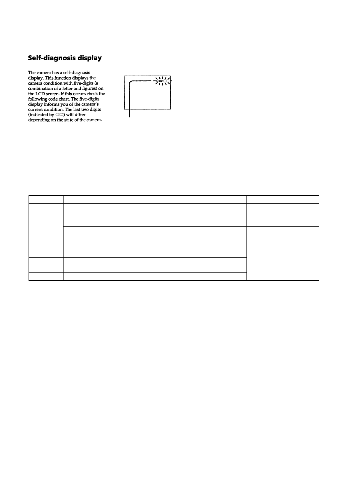
1-1. DESCRIPTION ON SELF-DIAGNOSIS DISPLAY
Self-diagnosis display
• C: ss: ss
You can reverse the camera
malfunction yourself. (However,
contact your Sony dealer or local
authorized Sony service facility
when you cannot recover from the
camera malfunction.)
• E: ss: ss
Contact your Sony dealer or local
authorized Sony service facility.
Display Code
C:32:ss
C:13:ss
E:61:ss
E:91:ss
E:92:ss
Countermeasure
Turn the power off and on again.
Format the “Memory Stick Duo” or
internal memory.
Insert a new “Memory Stick Duo”. “Memory Stick Duo” is broken.
Turn the power off and on again. Trouble with internal memory.
Checking of lens drive circuit.
Checking of flash unit or replacement
of flash unit.
Insert batteries correctly.
Trouble with hardware.
“Memory Stick Duo” or internal memory is
unformatted.
When failed in the focus and zoom
initialization.
Abnormality when flash is being
charged.
Batteries are not inserted correctly.
Cause
Caution Display During Error
SYSTEM ERROR
FORMAT ERROR
MEMORY STICK ERROR
INTERNAL MEMORY ERROR
—
DSC-S600_L2
1-1
Page 6
1-2. METHOD FOR COPYING OR ERASING THE DATA IN INTERNAL MEMORY
The data can be copied/erased by the operations on the Setup screen. (When erasing the data, execute formatting the internal memory.)
Note1: When replacing the SY-145 board, erase the data in internal memory of the board before replacement.
Note2: When replacing the SY-145 board or the IC203 on the SY-145 board, execute formatting and initialize the internal memory after replacement.
Method for Copying the Data in Internal Memory
Copy
Copies all images in the internal memory to a “Memory Stick Duo”.
OK
Cancel
1 Insert a “Memory Stick Duo” having 32 MB or larger capacity.
2 Select [OK] with v on the control button, then press z.
The message “All data in internal memory will be copied Ready?” appears.
3 Select [OK] with v, then press z.
Copying starts.
Use batteries with enough capacity or the AC Adaptor (not supplied). If you attempt to copy image files
using batteries with little remaining capacity, the batteries may run out, causing copying to fail or possibly
corrupting the data.
You cannot copy individual images.
The original images in the internal memory are retained even after copying. To delete the contents of the
internal memory, remove the “Memory Stick Duo” after copying, then execute the [Format] command in
(Internal Memory Tool) (page 46).
You cannot select a folder copied on a “Memory Stick Duo”.
Even if you copy data, a (Print order) mark is not copied.
See the following procedure.
Cancels the copying.
Method for Formatting the Internal Memory
This item does not appear when a “Memory Stick Duo” is inserted in the camera.
The default settings are marked with .
Format
Formats the internal memor y.
• Note that form a tting irrevocably erases all data in the internal memory, including even protected images.
OK
Cancel
1 Select [OK] with v on the control button, then press z.
The message “All data in internal memory will be erased Ready?” appears.
2 Select [OK] with v, then press z.
The format is complete.
See the following procedure.
Cancels the form a tting.
DSC-S600_L2
1-2
Page 7
1-3. PRECAUTION ON REPLACING THE SY-145 BOARD
• The Repair Board has already been adjusted. Re-initialization or EVR data copy from the set before repair is not required.
• Perform “Initial Language Data Check” mentioned below, and also the adjustment items necessary after SY Board replacement.
1-4. INITIAL LANGUAGE DATA CHECK
If the SY-145 board was replaced, initial language setting may be changed. Accordingly, change the following data so as to set same initial
language as that of the set distributing in each region.
Initial language: Language displayed at the next starting if the setting of Setup menu was reset.
It is different from the language setting selectable with the menu.
Initial Language Data
Page Address Data Language GP2 GP3 GP4
00 English zzz
04 Spanish zz
06 Portugal z
4F 8C
Note: GP2 is fixed to English.
GP3 is either English, Spanish, or Russian.
GP4 is either English, Spanish, Portugal, Simplified Chinese, or Korean.
08 Simplified Chinese z
0B Russian z
0D Korean z
Writing Method:
1) Select page: 00, address: 01 and set data: 01.
2) Select page: 4F, address: 8C, and set the Initial Language Data.
3) Select page: 40, address: 38, and set data: 00.
4) Click [Save] on the SEUS screen.
5) Select page: 80, address: 34, and check that the data is “00”.
6) Select page: 80, address: 30, and check that the data is “00”.
7) Select page: 00, address: 01, and set data: 00.
8) Turn off the camera.
9) Turn on the camera. Execute “Initialize” of Setup screen.
10) Check the language displayed when the camera starts.
1-5. HOW TO OPERATE THE CAMERA WITHOUT THE FRONT CABINET
Remove the LB-117 board from the cabinet (front) asembly, solder the leads to the SW-461 board, and fix the S101 switch (Lens barrier
open) to the ON position with an adhesive tape.
S101 switch
(Lens barrier open)
Adhesive tape
Cabinet (front) assembly
LB-117 board
LB-117 board
DSC-S600_L2
SW-461 board
Remove the claw
solder the leads
1-3E
Page 8

Link
Link
DISASSEMBLY
DISASSEMBLY
HELP
HELP
COMMON NOTE FOR DISASSEMBLY
COMMON NOTE FOR DISASSEMBLY
2. DISASSEMBLY
DSC-S600_L2
Page 9
NOTE FOR REPAIR
2. DISASSEMBLY
2. DISASSEMBLY
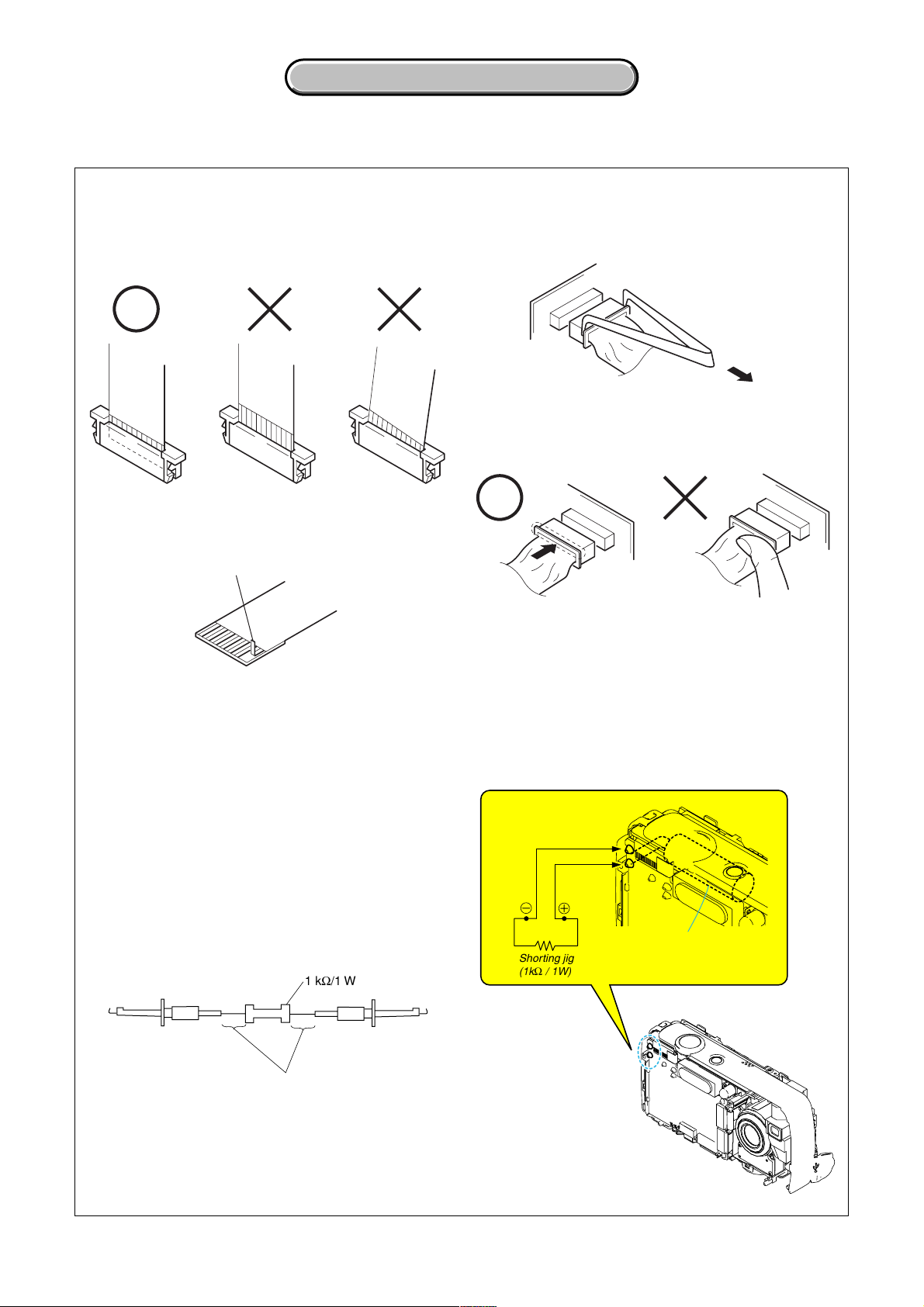
2. DISASSEMBLY
Make sure that the flat cable and flexible board are not cracked of
bent at the terminal.
Do not insert the cable insufficiently nor crookedly.
Cut and remove the part of gilt
which comes off at the point.
(Take care that there are
some pieces of gilt left inside)
When remove a connector, don't pull at wire of connector.
Be in danger of the snapping of a wire.
When installing a connector, don't press down at wire of connector.
Be in danger of the snapping of a wire.
DISCHARGING OF THE FLASHLIGHT POWER SUPPLY CAPACITOR
The charging elect capacitor 180uF (330V) is charged up to the
maximum 300 V potential.
There is a danger of electric shock by this high voltage when the
capacitor is handled by hand. The electric shock is caused by the
charged voltage which is kept without discharging when the main
power of the DSC-S600 is simply turned off. Therefore, the
remaining voltage must be discharged as described below.
Preparing the Short Jig
T o preparing the short jig. a small clip is a ttached to each end of
a resistor of 1 kW /1 W (1-215-869-11)
Wrap insulating tape fully around the leads of the resistor to
prevent electrical shock.
1 kΩ/1 W
Wrap insulating tape.
Discharging the Capacitor
Short circuits between the positive and the ne gative terminals of
charged capacitor with the short jig about 10 seconds.
Capacitor
Shorting jig
Ω
/ 1W)
(1k
SY-145
DSC-S600_L2
2-1
Page 10
4
(See page 2-5)
C
HELP 03
SY-145
3
5
2
1
Refer to page 2-1 "DISCHARGING OF
THE FLASHLIGHT POWER SUPPLY
CAPACITOR (LND904, LND905)",
when discharging the capacitor.
HELP 02
Three solderings2 Two solderings3 Open the BT cover.4 Open the cabinet (upper) assembly.5 Cabinet (front) assembly
1
2
7
8
SY-145
SY-145
4
2. DISASSEMBLY
2. DISASSEMBLY
HELP 01
3
(See page 2-5)
A
3
4
5
6
Flexible board (from the lens block assembly)6 Flexible flat cable (FFC-058)
Flexible flat cable (FFC-056)
SY-145 board, RL-063 board,
7
8
Two solderings2 Claw3 Two claws4 Flexible board (from the lens block assembly)
1
(See page 2-5)
B
speaker, microphone, etc.
5
1
6
8
2. DISASSEMBLY
2-1. DISASSEMBLY
The following flow chart shows the disassembly procedure.
7
Screw (M1.7x4) 6 Screw (M1.7x4) 7 Open the cabinet (upper) assembly.8 Cabinet (rear) assembly
5
5
Slide the BT cover.2 Screw (M1.7x4) 3 Open the USB cover.4 Screw (M1.7x4)
1
1
2
1
1
HELP 04
4
Screw (M1.7x4)2 Two claws3 RL-063 board
2
3
2
3
SY-145
Cabinet (upper) assembly
1
4
Two solderings2 Flexible board (from the LCD unit)
LCD unit
1
3
2-3 2-4
DSC-S600_L2
Page 11

5
2
4
SY-145
HN-015
Two solderings2 Elect 180uF (330V) capacitor
Three solderings4 Flash unit, harness (HN-015)
3
1
HELP 06
6
4
1
SY-145 board, RL-063 board,
3
5
flexible flat cable (FFC-056), etc.
Two solderings5 Miclophone holder
Miclophone
4
6
SY-145
5
HELP 05
3
2. DISASSEMBLY
2. DISASSEMBLY
3
4
5
2
2
1
Two solderings2 Speaker holder3 Speaker
1
3
2-5 2-6E
Flexible flat cable (FFC-058)
Flexible board (from the optical unit)
Screw (M1.7x4)4 LCD frame5 SW-461 board, flexible flat cable (FFC-058)
1
2
1
SW-461
RL-063
3
SY-145
Flexible board (from the lens block assembly)2 Flexible board (from the lens block assembly)3 Flexible board (from the optical unit)
Lens block assembly, optical unit.
1
4
4
SY-145
A
C
1
2
B
DSC-S600_L2
Page 12

HELP
Disassembling and assembling procedures that require attention are described here.
HELP 01
When installing the Cabinet (Rear) assembly, install it while aligning the
Mode switch of the
SW-461 board
with the position A of the Cabinet (Rear) assembly.
Mode Switch of
the SW-461 board
Cabinet (rear) assembly
A
HELP 02
Solder each lead according to the color (Y: yellow, G: gray, W: white, R: red, B: black) displayed on the SW-461 board.
Two reads
(from the BM-001 board)
Red
Tree reads
(from the LB-117 board)
Yellow
Gray
White
Black
DSC-S600_L2
SW-461 board
HELP
Page 13

HELP 03
SY-145
When installing the cabinet (front) asembly,
put the lead lines in the space between the
optical unit and the DC mortor.
Optical unit
DC mortor
When installing the cabinet (front) asembly,
put the lead lines in the space between
the tripod screw and the SW-461 board.
HELP 04
Solder each lead according to the color (R: red, B: black) displayed on the SY-145 board.
SW-461 board
Tripod screw
LCD leads
Black
Red
SY-145 board
DSC-S600_L2
HELP
Page 14

HELP 05
Solder each lead according to the color (R: red, B: black) displayed on the SY-145 board.
Mic unit
Black
Speaker
HELP 06
Give folding to the flexible flat cable (FFC-057).
RL-063 board
Red
SY-145 board
Flexible flat cable
(FFC-057)
DSC-S600_L2
Peak folding
Valley folding
Valley folding
Peak folding
SY-145 board
RL-063 board
Flexible flat cable
(FFC-057)
SY-145 board
HELP
Page 15

3. BLOCK DIAGRAMS
Link
Link
OVERALL BLOCK DIAGRAM POWER BLOCK DIAGRAM
OVERALL BLOCK DIAGRAM POWER BLOCK DIAGRAM
DSC-S600_L2
Page 16

3. BLOCK DIAGRAMS
3-1. OVERALL BLOCK DIAGRAM
CCD IMAGER and CD-606 FLEXIBLE BOARD are included in the LENS BLOCK ASSY (A-1156-857-A).
LENS UNIT
(LSV-951A)
IRIS MOTOR
SHUTER
IRIS
M
H
FOCUS MOTOR
M
ZOOM MOTOR
M
ZOOM RESET
SENSOR1
ZOOM RESET
SENSOR2
SHUTTER MOTOR
M
BM-001
BOARD
M001
LENS BARRIER
MOTOR
M
S101
LENS BARRIER
( )
OPEN
S102
LENS BARRIER
( )
CLOSE
LENSV OPEN
LENSV CLOSE
SW-461
BOARD
XLENSV
OPEN SENS
XLENSV
CLOSE SENS
LB-117 BOARD
FFC-056
(FLEXIBLE FLAT CABLE) (1/3)
BATTERY
HOLDER
LENS TEMP1
ZM SENS 1ST
ZM SENS 2ND
(1/3)
SENSOR
CD-606 FLEXIBLE BOARD
32-24,22,13-1133
LENS
LENS
TEMP2
TEMP1
24
23
22
20
19
5
3
1
14
21
4
26
33
5
8
12
10
14
11
18
15
CN401
24
23
25
26
CN006
BATT UNREG
BATT GND
CCD IMAGER
IRIS +
IRIS -
HALL +
HALL -
FOCUS +
FOCUS -
ZOOM A
ZOOM XA
ZOOM B
ZOOM XB
LENSV OPEN
LENSV CLOSE
SHUTTER+
SHUTTER-
OVF A
OVF B
OVF XA
OVF XB
X001
32.768KHz
UNREG
F002
F001
CN301
V1A,BV2V3A,BV4V5A,BV6V7A,B
F8
E8
A5
A8
H1
F2
E1
F1
D1
C1
F7
G7
D1
B1
F2
F3
E6
D6
A8
OSC I
A9
OSC O
B8
VL 3V
C7
XPWR ON
C9
USB VBUS
B10
XMS IN
( ) : Number in parenthesis ( ) indicates the division number of schematic diagram where the component is located.
X102
(2/8)
IC401
IRIS DRIVE
HALL AMP
FOCUS MOTOR DRIVE
ZOOM MOTOR DRIVE
LENS BARREIER
MOTOR DRIVE
SHUTTER DRIVE
IC402
OVF ZOOM DRIVE
(8/8)
IC001
DC/DC CONVERTER
REAL TIME CLOCK
IC004,005
2.9V/12V REG
V8
XDD RST OUT
VST
(2/8)
BATT SENS
XPWR OFF
(8/8)
B8
C7
F4
H6
H3
C2
G3
B1
H8
D6
B3
B4
B5
B6
C6
C5
SO
SI
SCK
F5
G4
G6
C5
C6
B6
D4
A7
B7
A4
SAN LENSV OPEN
SAN LENSV CLOSE
IRIS EN
IRIS IN
XSAN RST OUT
SAN 27M CLK0
SAN1 SO, SI, XSAN1SCK
ZM EN
ZM DIR A
ZM DIR B
MSHUT EN
MSHUT DIR
OVF EN
OVF DIR A
OVF DIR B
OVF A
OVF B
OVF XA
OVF XB
EVER 3.1V
EVER 2.9V
D 3.2V
A 3.2V
MS VCC
CAM 2.9V
D 1.8V
M 5V
D 1.2V
CAM -7.5V
BL H
BL L
XAF LED
A 2.9V
CAM 12V
ST UNREG
SY-145 BOARD
CCD OUT
8
60
IC301
H1A,B
19
37
H2A,B
17
40
RG
20
44
18
48
3
53
CN301
11,8
16,12
9,91
5,6
88,102
90,79,76
92
S/H
A/D CONV.
TIMING
GENERATOR
89 93
97,98,100,101
103,104,105,3
2,4,7,10,14,18
(1/8)
56
77
80
SAN1 SO,XSAN1SCK
(4/8) (4/8)
IC201
FLASH MEMORY
D0-D15
SAN0 SO, SI, XSAN0SCK
BURST
IC202
A1-A21
CA AD0 - CA AD13
CLK TGO
CA HD CA FD
(4/8)
256Mbit
SDRAM
D0-D15
CPU_D0-D15
CPU_A1-A21,A25
33.75MHz
XTAL OSC
X101
12MHz
XTAL OSC
IC203
SUPER AND
FLASH MEMORY
CLKTGEXT
EXTAL
D0-D31
A0-A12
DSP QCLK
SAN 27M CLKO
A20,A21,A25
IRIS EN
IRIS IN
ZM EN
ZM DIR A
ZM DIR B
SAN LENSV OPEN
SAN LENSV CLOSE
MSHUT EN
MSHUT DIR
OVF EN
OVF DIR A
OVF DIR B
ZM SENS 1ST
ZM SENS 2ND
LENS TEMP1
LENS TEMP2
XLENSV OPEN SENSE
XLENSV CLOSE SENSE
C1
K5,G4,H4,L5
H2,H1,J1,J2
M5,J4,K4,M6
K2,K1
A6
IC101
E1
SYSTEM CONTROL
F2
H5
J5
D21,D22,D20,B22,A22,A23,
B23,E20,E21,B24,A24,A25,
B25,C25,C26,B26,E10,A10,
D10,E11,B10,A11,B11,E12,
D11,D12,F12,B12,A12,E13,
D13,D14
D17,D18,D16,B18,A19,
B19,E16,D19,E19,E17,
B20,A20,E18
A18
AF9
AB13,AA13,AE13,AF13,
AF12,AE12,AA12,AC12,AC11,
AB12,AE11,AF11,AE10,AB11,
AC10,AB10
AF21,AF20,AE20,AB18,AB19,
AC19,AB16,AE19,AF19,AF18,
AE18,AA15,AC18,AC17,AB15,
AE17,AF17,AE16,AB14,AC16,
AC15,AE14
N4
P4
N2
N6
M2
AC14
AA14
R5
R25
AB5
SO
AA5
SI
SCK
Y5
K25
BATT SENS
R26
XDD RST OUT
Y4
AA23
XPWR OFF
L4
L2
N5
V4
U5
J25
K22
Y22
AC23
SAN1 SO, SI, SCK
(3/8)
CAMERA DSP
AC4,AE4
AE5,AC5
AB6,AF6
E8,E7,D6
D5,E6,B4
U2
R6
AF4
R22
V23
AB22
N21
P23
D23
L22
K23
L23
AC1
AD1
F22
E22
Y26
L26
K26
E4
E9
B8
D9
T2
R4
U4
SAN1 SO, SI, SCK, XSAN1SCK
OVF SENS
XAE LOCK LED
XSTRB LED
XCS_AUDIO
SAN1 SO, XSAN1SCK
AUIN
AUOUT
MS D0-MS D3, MS BS, MS CLK
XACCESS LED
LCD HD
LCD VD
LCD CK
XSAN RST OUT
STRB CHG
XSTRB FULL
STRB CHG CONT
STRB ON
XAE LOCK SW
XSHUTTER SW
XPWR LED
MODE DIAL 0
KEY AD0
KEY AD1
USB DP, USB DM
E4
F3
E3
IC601
E6
MIC AMP
E5
SPEAKER AMP
LCD D2-D7
SAN1 SO, XSAN1SCK
(5/8)
FFC-056
(FLEXIBLE FLAT CABLE) (2/3)
SW-461 BOARD (2/3)
CN006
BL H
BL L
LCD901
2.0 INCH
COLOR DIGITAL
LCD PANEL
HIGH VOLTAGE
CHAGER
IC901
IGBT DRIVE
D003
(ACCESS)
MS D0-MS D3, MS BS, MS CLK
XMS IN
LCD
BACK
LIGHT
T901
1
2
(6/8)
Q901
FLASH
DRIVE
4,3,5,7,2,8
D901
(RECT)
CN002
MEMORY
STICK
Duo
6
CONNECTOR
XE A(H)
FLASH
XE K(L)
C9001
MAIN
CAPACITOR
UNIT
XENON
( )
TUBE
TRIGGER
COIL
13,12,14,16,11,17
17
|
22
24
25
23
27
26
30
CN1001
15
10
9
6
4 7
8
15
ST UNREG
FFC-057 (FLEXIBLE FLAT CABLE)
S201
7
6
3
XPWR ON
2
XAF LED
8
FFC-056 (FLEXIBLE FLAT CABLE) (3/3)
MOVIE / STILL / PLAY
20
S001, 004, 002, 005, 003
22
DOWN, RIGHT, UP, LEFT, SET
21
DISPLAY, DUST, MENU, ZOOM WIDE, ZOOM TELE
2
3
USB VBUS
5
VL 3V
6
CN006
OVF SENS
OVF A
OVF B
OVF XA
OVF XB
MIC SIG
SP+
SP-
D002 (AE LOCK)
D001 (FLASH)
1
2
B6
A5
A2
8
6
|
3
CN703
FFC-058 (FLEXIBLE FLAT CABLE)
SHUTTER
S202
POWER
S011
S007, 009, 008, 010, 006
CN001
MIC901
MIC
MICROPHONE
SP901
SPEAKER
RL-063 BOARD
D201 (POWER)
SW-461
BOARD
(3/3)
BT001
LITHIUM
BATTERY
(SECONDARY)
OVF RESET
7
SENSOR
4
OVF ZOOM
|
M
MOTOR
1
LED901
(AF LED)
3,2
D+, D-
1
OPTICAL
VIEWFINDER
UNIT
CN003
(USB)
DSC-S600_L2
3-1 3-2
Page 17

3-2. POWER BLOCK DIAGRAM
( ) : Number in parenthesis ( ) indicates the division number of schematic diagram where the component is located.
FFC-056
(FLEXIBLE FLAT CABLE)
CN002
MEMORY
STICK
Duo
CONNECTOR
OPTICAL
VIEWFINDER
UNIT
OVF RESET
SENSOR
FFC-058
(FLEXIBLE FLAT CABLE)
RL-063
BOARD
LED901
(AF LED)
FFC-057
(FLEXIBLE FLAT CABLE)
BATTERY
HOLDER
BT001
LITHIUM
BATTERY
(SECONDARY)
SW-461
BOARD
9
RST VCC
CN001
D201 (POWER)
S202
POWER
VL 3V
D001 (FLASH)
R009
CN006
BATT UNREG
BATT GND
6
D 3.2V
9
MS VCC
18
XSTRB LED
2
D 3.2V
98
CN703
XPWR LED
3
D 3.2V
4
XPWR ON
2
XAF LED
8
SY-145 BOARD
F001
STRB CHG
XSTRB FULL
STRB CHG CONT
D 3.2V
A 2.9V
D 1.2V
D 1.8V
D 3.2V
F002
R22
V23
AB22
P25
D23
E22
R002
-7.5V ON
XPWR LED
XSTRB LED
L201
(4/8)
IC201
BURST
FLASH MEMORY
(3/8)
IC101
CAMERA DSP
SYSTEM CONTROL
SD 1.8V
EVER 2.8V
XCS DD
SAN0 SO
SAN0 SI
XSAN0 SCK
D001
AA23
W23
AB5
AA5
IC202
IC203
SUPER AND
FLASH MEMORY
K25
R26
Y4
T25
Y5
(4/8)
256Mbit
SDRAM
(4/8)
R041
X001
32.768KHz
BATT SENS
XDD RST OUT
XPWR OFF
MS PWR ON
VL 3V
XPWR ON
ST UNREG
UNREG
(8/8)
IC001
DC/DC CONVERTER
REAL TIME CLOCK
J1
UNREG1-1,2
K1
LDO1
H1
3.1V REG
B8
RTC BAT
A8
OSC I
A9
OSC O
D4
DTG1
A7
XRESET
B7
XPWR OFF
MS PWR ON
D3
XCS DD
A6
SAN0 SO
C5
SAN0 SI
C6
XSAN0 SCK
B6
XPWRON1
C7
A4
XAF LED
-7.5V ON
D 3.2V
A 2.9V, D 1.8V, D 1.2V, MS VCC
2.9V REG
1.8V REG
PWR1-1
PWR1-2
PWR1-3
MS PWR IN
MS PWR
LDO3IN
LDO2IN
UNREG2
PWR56 OUT
ST UNREG
STRB CHG
XSTRB FULL
STRB CHG CONT
D901
T901
L901
15
(6/8)
10
9
IC901
6
HIGH VOLTAGE
M5V
CHAGER
IGBT DRIVE
3
(RECT)
1
2
XE A(H)
FLASH
UNIT
XENON
( )
TUBE
C9001
MAIN
CAPACITOR
(8/8)
4
3
BL H
BL L
Q003
SWITCH
IC004
1
2.9V REG
(8/8)
3
IC005
5
Q004
21
12V REG
54
-7.5V
L009
A1
B1
C2
F1
VO1-1
VO1-2
F2
H2
VFB1
L002
G1
G2
B2
LDO3
A2
B3
LDO2
A3
J6
K6
J7
K7
L006
J9
LX5-1
J10
LX5-2
K9
LX5-3
K10
LX5-4
H9VFB5
H6GT6
H7VFB6
D10
PWR2
C10
LX2
D8
VFB2
E10
LX3
E9VO3
LV3
F9
RS3
F8
SWITCHING
G9BG4
F10
TG4
F7VFB4
G8
PSG4
15V
D003
(RECT)
L003
L005
Q001
(RECT)
SWITCHING & RECT
F003
D002
L008
145
2
3
Q002
RECT
A 2.9V
3
D 3.2V
MS VCC
CAM 2.9V
D 1.8V
PANEL 15V
Q005, 006
1
-7.5V ON
D 1.2V
M 5V
M 5V
D 3.2V
CAM 12V
CAM -7.5V CAM -7.5V CD
D 3.2V
PANEL 15V
D 3.2V
D 3.2V
D 1.8V
A 2.9V
(5/8)
IC601
MIC AMP
SPEAKER AMP
(1/8)
IC301
S/H
A/D CONV.
TIMING GENERATOR
L301
D 3.2V
(2/8)
IC401
IRIS DRIVE
FOCUS MOTOR DRIVE
ZOOM MOTOR DRIVE
(2/8)
M 5V
IC402
SHUTTER DRIVE
OVF ZOOM DRIVE
L1002
L1001
Q1001
D 3.2V
DETECT
D1002
CCD IMAGER and CD-606 FLEXIBLE BOARD
are included in the LENS BLOCK ASSY (A-1156-857-A).
CD-606
FLEXIBLE BOARD
CAM 15V CD
5
CCD IMAGER
1
CN301
LENS UNIT
(LSV-951A)
R402
ZM RST1 VCC
ZM RST2 VCC
VCC1
VGH
VDD
LCD
BACK LIGHT
LCD901
2.0 INCH
COLOR DIGITAL
LCD PANEL
ZOOM
RESET1
SENSOR
ZOOM
RESET2
SENSOR
13
R401
8
CN401
BL H
BL L
9
10
11
CN1001
Q1002
DSC-S600_L2
3-3 3-4E
Page 18

4-1. FRAME SCHEMATIC DIAGRAM
1
4. PRINTED WIRING BOARDS AND SCHEMATIC DIAGRAMS
121152 1413103679 16
1548
A
B
C
D
LCD BACK LIGHT
(Included in the LCD901)
E
LCD901
2.0 INCH
COLOR DIGITAL LCD PANEL
F
G
H
I
J
K
L
M
N
O
16
DSC-S600_L2
SP901
SPEAKER
MIC901
MICROPHONE
RL-063 BOARD
BATTERY
HOLDER
BATT_GND
BATT_UNREG
LND002
LND001
33PCN1001
33
VCOM
32
VSS
TEST
31
30
XRESET
29
BLON
28
XCS
27
SI
XSCK
26
25
XVD
XHD
24
23
DCK
D5
22
21
D4
D3
20
D2
19
18
D1
D0
17
16
BL_H
BL_L
HN-007 HARNESS
HN-006 HARNESS
HN-009 HARNESS
HN-008 HARNESS
MIC
CN002
MEMORY
STICK Duo
CONNECTOR
CN003
USB
N.C.
N.C.
15
VBC
14
VSH
13
COMDC
12
11
VDD
VGH
10
VCC1
9
C2+
8
C2-
7
VGL
6
N.C.
5
N.C.
4
COMOUT
3
VVCOM
2
VSS
1
LND003
BL_L
LND004
BL_H
LND604
SP-
LND603
SP+ FOCUS+
LND602
MIC_SIG
LND601
MIC_GND
10
GND
9
VCC
8
SCLK
DATA3
7
INT
6
DATA2
5
4
SDIO/DATA0
3
DATA1
2
BS
1
GND
GND
5
4ID
3
D+
2
D-
1
VCC
SY-145 BOARD
(1/8)CAMERA A/D CONV.TIMING GENERATOR
(2/8)LENS DRIVE
(3/8)CAMERA DSP,SYSTEM CONTROL
(4/8)SUPER AND,FLASH MEMORY,SDRAM
(5/8)ADUIO AMP,MIC,SP
(6/8)FLASH DRIVE
(7/8)LCD PANEL,CONNECTOR
(8/8)DC/DC CONVERTER
26
26P
CN006
REG_GND
GND
D+
VL_3V
VCC
D-
GND
123456789
123456789
D-
D+
VCC
GND
GND
VL_3V
REG_GND
SW-461 BOARD
XACCESS_LED
MS_BS
D_3.2V
REG_GND
1011121314151617181920212223242526
FLEXIBLE
FLAT CABLE
1011121314151617181920212223242526
D_3.2V
MS_BS
REG_GND
XACCESS_LED
(FLASH)
(CAPACITOR)
HN-015 HARNESS
C9001
MS_D0
XMS_IN
MS_D3
KEY_AD0
REG_GND
MODE_DIAL0
KEY_AD1
MS_CLK
MS_D1
MS_D2
MS_VCC
MS_D2
MS_D3
MS_D1
MS_D0
XMS_IN
MS_CLK
MS_VCC
REG_GND
MODE_DIAL0
KEY_AD1
KEY_AD0
LENSV_OPEN
LENSV_CLOSE
LENSV_OPEN
LENSV_CLOSE
XLENSV_CLOSE_SENSE
XLENSV_OPEN_SENSE
XLENSV_OPEN_SENSE
XLENSV_CLOSE_SENSE
BT001
LITHIUM
BATTERY
(SECONDARY)
4-1
XSHUTTER_SW
N.C.
XAE_LOCK_SW
XAF_LED
9P
FFC-057
FLEXIBLE
FLAT CABLE
N.C.
XAF_LED
XAE_LOCK_SW
XSHUTTER_SW
9P
XE_A(H)
TRIGGER
XE_K(L)
MAIN CON+
MAIN CON-
10PCN703
ZM_OVF_XB
ZM_OVF_XA
XAE_LOCK_LED
XSTRB_LED
123456789
FFC-058FFC-056
FLEXIBLE
FLAT CABLE
123456789
XSTRB_LED
ZM_OVF_XB
ZM_OVF_XA
XAE_LOCK_LED
10P
REG_GND
REG_GND
ZM_OVF_B
ZM_OVF_B
D_3.2V
XPWR_LED
N.C.
XPWR_ON
123456789
123456789
N.C.
D_3.2V
XPWR_ON
XPWR_LED
LND906
LND908
LND907
LND904
LND905
OVF_SENS
EMITTER
N.C.
RST_VCC
ZM_OVF_A
10
10
N.C.
EMITTER
RST_VCC
OVF_SENS
ZM_OVF_A
33PCN301
1CAM-7.5V-CD
LENS ASSY
2REG_GND
3RG
CCD IMAGER and CD-606 FLEXIBLE BOARD are
4REG_GND
included in the LENS BLOCK ASSY(A-1156-857-A).
5CAM15.0V-CD
and it is not supplied as an independent
6POWER_SAVE
service parts.
7REG_GND
8CCD_OUT
9CCD_GND
10REG_GND
11V8
12V7B
13V7A
14VSUB_CONT
15SHT
CD-606
16REG_GND
FLEXIBLE
17H1B
BOARD
18H2B
19H1A
20H2A
21REG_GND
22V6
23VHLD
24V5B
25V5A
26V4
27VST
28V3B
29V3A
30V2
31V1B
32V1A
33TH2
33PCN401
NC
1
NC
2
HALL-
3
4
BIAS+
HALL+
5
6
BIAS-
NC
7
ZM_RST2_VCC
8
PT_E/LED_K2
9
ZM_SENS_OUT2
10
11
PT_E/LED_K1
12
ZM_SENS_OUT1
13
ZM_RST1_VCC
14
15
SHUTTER-
SHUTTER-
16
SHUTTER+
17
18
SHUTTER+
ND-
19
ND-
20
21
FOCUS-
ND+
22
ND+
23
TH1
24
GND2
25
ZOOM_A
26
ZOOM_A
27
ZOOM_XA
28
ZOOM_XA
29
ZOOM_XB
30
ZOOM_XB
31
ZOOM_B
32
ZOOM_B
33
CN001
8P
8
RST_VCC
OVF_SENS
7
6
XOVF_RST_LED
EMITTER
5
ZM_OVF_A
4
ZM_OVF_B
3
2
ZM_OVF_XA
ZM_OVF_XB
1
HN-011 HARNESS
LENSV_CLOSE
LND037
LND038
LND039
LND040
LND041
LENSV_OPEN
XLENSV_OPEN_SENSE
XLENSV_CLOSE_SENSE
REG_GND
HN-010 HARNESS
HN-012 HARNESS
HN-013 HARNESS
HN-014 HARNESS
CCD IMAGER
(6M)
OPTICAL
VIEW FINDER
UNIT
LND401
LENSV_CLOSE
LENSV_OPEN
LND402
BM-001 BOARD
XLENSV_OPEN_SENSE
LND101
LND102
REG_GND
LND103
XLENSV_CLOSE_SENSE
LND403
LENSV_CLOSE
LENSV_OPEN
LND404
LB-117 BOARD
LENS
BARRIER
MOTOR
M001
4-2
FRAME SCHEMATIC DIAGRAM
Page 19

Link
Link
4-2. SCHEMATIC DIAGRAMS
BM-001 BOARD
BM-001 BOARD
LB-117 BOARD
LB-117 BOARD
COMMON NOTE FOR SCHEMATIC DIAGRAMS
COMMON NOTE FOR SCHEMATIC DIAGRAMS
(LENS OPEN/CLOSE MOTOR)
(LENS OPEN/CLOSE MOTOR)
(OPEN/CLOSE SWITCH)
(OPEN/CLOSE SWITCH)
RL-063 BOARD
RL-063 BOARD
SW-461 BOARD
SW-461 BOARD
(JACK, FUNCTION SW, LITHIUM BATTERY)
(JACK, FUNCTION SW, LITHIUM BATTERY)
(POWER SWITCH)
(POWER SWITCH)
DSC-S600_L2
Page 20

4-2. SCHEMATIC DIAGRAMS
4-2. SCHEMATIC DIAGRAMS
4-2. SCHEMATIC DIAGRAMS
THIS NOTE IS COMMON FOR SCHEMATIC DIAGRAMS
(In addition to this, the necessary note is printed in each block)
(For schematic diagrams)
• All capacitors are in µF unless otherwise noted. pF : µ
Link
µF. 50 V or less are not indicated except for electrolytics
and tantalums.
• Chip resistors are 1/10 W unless otherwise noted.
kΩ=1000 Ω, MΩ=1000 kΩ.
• Caution when replacing chip parts.
New parts must be attached after removal of chip.
Be careful not to heat the minus side of tantalum
capacitor, Because it is damaged by the heat.
• Some chip part will be indicated as follows.
Example C541 L452
22U 10UH
TA A 2520
1. Connection
Pattern box Color bar chart
Pattern box
Pattern box PTB-450
J-6082-200-A
or
Small pattern box
PTB-1450
J-6082-557-A
L = 1 m (PTB-450)
L = 40 cm (PTB-1450)
For PTB-450:
J-6020-250-A
For PTB-1450:
J-6082-559-A
Front of the lens
Kinds of capacitor
Temperature characteristics
External dimensions (mm)
• Constants of resistors, capacitors, ICs and etc with XX
indicate that they are not used.
In such cases, the unused circuits may be indicated.
• Parts with * differ according to the model/destination.
Refer to the mount table for each function.
• All variable and adjustable resistors have characteristic
curve B, unless otherwise noted.
• Signal name
XEDIT → EDIT PB/XREC → PB/REC
• 2: non flammable resistor
• 5: fusible resistor
• C: panel designation
• A : B+ Line
• B : B– Line
• J : IN/OUT direction of (+,–) B LINE.
• C: adjustment for repair.
• Circled numbers refer to waveforms.
(Measuring conditions voltage and waveform)
• Voltages and waveforms are measured between the
measurement points and ground when camera shoots
color bar chart of pattern box. They are reference values
and reference waveforms.
(VOM of DC 10 MΩ input impedance is used)
• Voltage values change depending upon input
impedance of VOM used.)
Precautions for Replacement of imager
• If the imager has been replaced, carry out all the
adjustments for the camera section.
• As the imager may be damaged by static electricity from
its structure, handle it carefully like for the MOS IC.
In addition, ensure that the receiver is not covered with
dusts nor exposed to strong light.
L
Camera
2. Adjust the distance so that the output waveform of
Fig. a and the Fig. b can be obtain.
H
Yellow
Cyan
White
Magenta
Green
AABBA=B
Fig. a (Video output terminal output waveform)
Fig.b (Picture on monitor TV)
Red
Blue
Electronic beam
scanning frame
CRT picture frame
When indicating parts by reference number, please
include the board name.
Note :
The components identified by
mark 0 or dotted line with mark
0 are critical for safety.
Replace only with part number
specified.
Note :
Les composants identifiés par
une marque 0 sont critiques
pour la sécurité.
Ne les remplacer que par une
pièce portant le numéro spécifié.
DSC-S600_L2
4-3
Page 21

4-2. SCHEMATIC DIAGRAMS
1
BM-001 BOARD
LENS OPEN/CLOSW MOTOR
A
XX MARK:NO MOUNT
TO
SW-461
BOARD
(PAGE 4-7)
HN-011 HARNESS
HN-010 HARNESS
B
16
1
LB-117 BOARD
OPEN/CLOSE SWITCH
A
XX MARK:NO MOUNT
TO
SW-461
BOARD
(PAGE 4-7)
B
HN-012 HARNESS
HN-013 HARNESS
HN-014 HARNESS
2
LENSV_CLOSE LENSV_CLOSE
LENSV_OPEN
LND401
LND402 LND404
2
LENS BARRIER
3P
XLENSV_OPEN_SENS
REG_GND
XLENSV_CLOSE_SENS
LND101
1
LND102
2
LND103
3
OPEN
435
LND403
LENSV_OPEN
43
S102S101
LENS BARRIER
CLOSE
1
2
35
4
RL-063 BOARD
POWER SWITCH
A
XX MARK:NO MOUNT
M001
+
LENS
M
BARRIER
MOTOR
–
TO
SY-145
BOARD(7/8)
THROUGH
B
THE FFC-057
FLEXIBLE
FLAT CABLE
(PAGE 4-21
of LEVEL3)
9P
XPWR_ON
XPWR_LED
D_3.2V
REG_GND
XSHUTTER_SW
XAE_LOCK_SW
XAF_LED
N.C.
1
2
3
4
5
6
7
8
N.C.
9
S202
POWER
D201
SML-412MWT86
POWER
S201
SHUTTER
C
16
1
2
4
3
6
5
4
2
1
3
LED901
LND208
XAF_LED
D_3.2V
LND209
(AFLED)
16
DSC-S600_L2
4-5
4-6
BM-001/LB-117/RL-063
Page 22

• Refer to page 4-3 for mark 0.
1
2 9
SW-461 BOARD
JACK,FUNCTION SW,LITHIUM BATTERY
XX MARK:NO MOUNT
A
CN006 26P
B
XACCESS_LED
TO
C
D
SY-145
BOARD(7/8)
THROUGH
THE FFC-056
FLEXIBLE
FLAT CABLE
(PAGE 4-21
of LEVEL3)
MODE_DIAL0
LENSV_CLOSE
LENSV_OPEN
XLENSV_OPEN_SENSE
XLENSV_CLOSE_SENSE
E
2P
LENSV_CLOSE
LENSV_OPEN
3P
XLENSV_OPEN_SENSE
XLENSV_CLOSE_SENSE
10P
XAE_LOCK_LED
F
G
TO
BM-001
BOARD
(PAGE 4-5)
TO
LB-117
BOARD
(PAGE 4-5)
16
HN-011 HARNESS
HN-010 HARNESS
HN-012 HARNESS
HN-013 HARNESS
HN-014 HARNESS
TO
SY-145
BOARD(7/8)
CN703
THROUGH
THE FFC-058
FLEXIBLE
FLAT CABLE
(PAGE 4-21
of LEVEL3)
(LITHIUM BATTERY)
(SECONDARY)
FB001
FB002
FB003
FB004
FB005
D001
(FLASH)
SML-310YTT86
C002
XX
R009
1500
4
BT001
0uH
0uH
0uH
0uH
0uH
D002
(AELOCK)
SML-510MWT86S
C003
0.01u
B
1
2
3
4
5
6
7
8
D003
SML-512UWT86
R007
1k
FB006
CN001 8P
ZM_OVF_XB
ZM_OVF_XA
ZM_OVF_B
ZM_OVF_A
EMITTER
XOVF_RST_LED
OVF_SENS
RST_VCC
(ACCESS)
0uH
C004
XX
R008
C001
0.1u
1k
B
3
D004
MAZW068H0LS0
10
1
35
GND
1
D+
2
D-
3
GND
4
VCC
5
VL_3V
6
7
REG_GND
8
D_3.2V
9
REG_GND
10
MS_BS
11
12
MS_D0
13
MS_D2
14
XMS_IN
15
MS_D3
16
MS_CLK
17
MS_VCC
18
REG_GND GND
19
20
21
KEY_AD1
KEY_AD0
22
23
24
25
26
LND037
1
LND038
2
LND039
1
LND040
2
REG_GND
XSTRB_LED
ZM_OVF_XB
ZM_OVF_XA
ZM_OVF_B
ZM_OVF_A
EMITTER
OVF_SENS
RST_VCC
LND041
3
1
2
3
4
5
6
7
8
9
N.C.
10
R001
33
FB007
0uH
610
R015
XX
D007
XX
10P
GND
1
BS
2
DATA1MS_D1
3
4
SDIO/DATA0
5
DATA2
6
INT
7
DATA3
SCLK
8
VCC
9
S001
DOWN
43
2200x4
S002
21
43
2
21
43
21
OPTICAL VIEWFINDER UNIT is replaced as a block.
So that there PRINTED WIRING BOARD and
SCHEMATIC DIAGRAM are omitted.
OPTICAL
VIEWFINDER
UNIT
S003
87
UP
21
SET
RB001
CN002
MEMORY
STICK Duo
CONNECTOR
S004
RIGTH
34
S005
12
LEFT
34
12
7
24
13
LF001
0uH
8
5P
GND
5
4ID
3
D+
2
D-
1
VCC
R012
1k
STATIC_GND
STATIC_GND
S007
DISPLAY
43
S008
21
MENU
43
21
S006
ZOOM TELE
43
21
CN003
USB
LND045
STATIC_GND
LND043
STATIC_GND
LND042
LND044
S011
PLAY-STILL-MOVIE
16
D006
XX
RB002
2200x4
87
21
S009
DUST
34
12
S010
ZOOM WIDE
34
12
D005
6.8B
78
12
RB003
2200x4
Schematic diagram of the SY-145 board is not shown.
Pages from 4-9 to 4-24 are not shown.
DSC-S600_L2
4-7 4-8
SW-461
Page 23

4-3. PRINTED WIRING BOARDS
Link
Link
BM-001 BOARD RL-063 BOARD
BM-001 BOARD RL-063 BOARD
LB-117 BOARD SW-461 BOARD
LB-117 BOARD SW-461 BOARD
COMMON NOTE FOR PRINTED WIRING BOARDS
COMMON NOTE FOR PRINTED WIRING BOARDS
MOUNTED PARTS LOCATION
MOUNTED PARTS LOCATION
DSC-S600_L2
Page 24

4-3. PRINTED WIRING BOARDS
4-3. PRINTED WIRING BOARDS
4-3. PRINTED WIRING BOARDS
THIS NOTE IS COMMON FOR WIRING BOARDS
(In addition to this, the necessary note is printed in each block)
(For printed wiring boards)
•
•
: Uses unleaded solder.
: Pattern from the side which enables seeing.
(The other layers’ patterns are not indicated)
• Through hole is omitted.
• Circled numbers refer to waveforms.
• There are a few cases that the part printed on diagram
isn’t mounted in this model.
• C: panel designation
• Chip parts.
Transistor Diode
C
EB
5
5246
654
45
123
31
21
345
312
43
12
12
534
3
54
21
21
34
5
21321
4
123
43
12
64
3
43
12
3
31
4625
4
3
12
1
3
12
3
1
DSC-S600_L2
4-25
Page 25

4-3. PRINTED WIRING BOARDS
BM-001 (2 layers), LB-117 (2 layers), RL-063 (2 layers)
• : Uses unleaded solder.
BM-001 BOARD
LND403
LND404
LND402
LND401
1-868-243-
LB-117 BOARD
LND103
M001
M
(LENS BARRIER)
11
RL-063 BOARD
41
9
FFC-057
1
3
S201
5
6
2
SHUTTER
AK
D201
(POWER)
3
4
S202
POWER
1
1-867-293-
2
LND209
LED901
(AF LED)
LND208
11
DSC-S600_L2
LND102
LND101
S101
LENS BARRIER
OPEN
LENS BARRIER
S102
CLOSE
11
1-867-722-
4-27 4-28
BM-001/LB-117/RL-063
Page 26

SW-461 (2 layers)
: Uses unleaded solder.
•
A
B
SW-461 BOARD(SIDE A)
CN006
26
FB003
FB004
FB005
10
LND044
R008
MEMORY STICK Duo
CONNECTOR
C001
12
FB002
CN002
FB001
R001
1
1
11
1
FFC-058
SW-461 BOARD(SIDE B)
MOVIE-STILL-PLAY
10
10
9
LITHIUM BATTERY
(SECONDARY)
6
BT001
S011
+
–
8
7
1
CAUTION :
Danger of explosion if battery is incorrectly replaced.
C004
FB006
C003
C002
R009
1-867-292-
LND045
5
1
11
8
CN001
1
7
CN003
6
Replace only with the same or equivalent type.
(USB)
DSC-S600_L2
C
D
3
4
S009
1
2
DUST DISPLAY
1
S004
3
2
3
2
1
RB003
D003
AK
(ACCESS)
2
4
UP
D004
D006
1
8
7
D007
D005
4
S001
123
DOWN
234
S003
1
SETRIGHT LEFT
3
4
S002
1
2
RB002
7
82
1
R007
1
R015
3
3
4
S005
1
2
7
8
1
RB001
1
2
3
S007
S008
R012
LND043
3
12
1-867-292-
LND037
LND038
FB007
4
LF001
LND039
LND040
LND041
2
4
2
MENU
4
11
Printed wiring board of the SY-145 board is not shown.
Pages from 4-31 to 4-34 are not shown.
ZOOM
4
TELE
E
16
S006
123
LND042
12345
S010
123
4
ZOOM
WIDE
4-29 4-30
D001
(FLASH)
AK
D002
(AE LOCK)
AK
Waveforms of the SY-145 board is not shown.
Page 4-35 is not shown.
SW-461
Page 27

4-3. PRINTED WIRING BOARDS
4-3. PRINTED WIRING BOARDS
4-5. MOUNTED PARTS LOCATION
SW-461 BOARD
BT001 A-3
C001 A-1
C002 B-5
C003 A-4
C004 A-4
CN001 A-5
CN002 A-1
CN003 B-5
CN006 A-1
* D001 E-4
* D002 E-4
* D003 D-1
* D004 D-1
* D005 D-1
* D006 D-1
* D007 D-1
FB001 A-2
FB002 A-1
FB003 A-1
FB004 A-1
FB005 A-1
FB006 A-4
* FB007 D-5
* LF001 D-5
* LND037 D-5
* LND038 D-5
* LND039 D-5
* LND040 D-5
* LND041 D-5
* LND042 E-1
* LND043 C-5
LND044 B-1
LND045 B-5
R001 A-2
* R007 C-2
R008 A-1
R009 B-5
* R012 D-5
* R015 C-2
* RB001 D-2
* RB002 D-1
* RB003 D-1
* S001 C-1
* S002 D-1
* S003 D-1
* S004 D-1
* S005 D-2
* S006 E-1
* S007 C-2
* S008 D-2
* S009 C-1
* S010 E-2
no mark : side A
* mark : side B
DSC-S600_L2
Mounted parts location of the SY-145 board is not shown.
Page 4-37 is not shown.
4-36E
SW-461
Page 28

NOTE
NOTE
5. REPAIR PARTS LIST
NOTE: Characters A to Z of the electrical parts list indicate location of exploded views in which the desired part is shown.
Link
Link
OVERALL SECTION
OVERALL SECTION
Link
Link
LB-117 BOARD
LB-117 BOARD
A
D
EXPLODED VIEWS
EXPLODED VIEWS
S
Y
-1
4
5
BATTERY HOLDER
BATTERY HOLDER
SECTION
SECTION
ELECTRICAL PARTS LIST
ELECTRICAL PARTS LIST
A
D
RL-063 BOARD
RL-063 BOARD
SW-461 BOARD
SW-461 BOARD
B
C
E
B
E
ACCESSORIES
ACCESSORIES
SY-145 BOARDBM-001 BOARD
SY-145 BOARDBM-001 BOARD
C
DSC-S600_L2
Page 29

5. REPAIR PARTS LIST
5. REPAIR PARTS LIST
5. REPAIR PARTS LIST
NOTE:
• -XX, -X mean standardized parts, so they may have some differences from
the original one.
• Items marked “*” are not stocked since they are seldom required for routine
service. Some delay should be anticipated when ordering these items.
• The mechanical parts with no reference number in the exploded views are not
supplied.
• Due to standardization, replacements in the parts list may be different from
the parts specified in the diagrams or the components used on the set.
• CAPACITORS:
uF: µF
• COILS
uH: µH
• RESISTORS
All resistors are in ohms.
METAL: metal-film resistor
METAL OXIDE: Metal Oxide-film resistor
F: nonflammable
• SEMICONDUCTORS
In each case, u: µ, for example:
uA...: µA... , uPA... , µPA... ,
uPB... , µPB... , uPC... , µPC... ,
uPD..., µPD...
CAUTION1 :
For the part of 51: TAPE, FFC FIXED (2-662-566-01) , cut WOVEN (T0.25),
FABRIC NON (3-706-631-01) into the desired length and use it.
CAUTION2 :
For the part of 58: TAPE, MOUNT PARTS FIXED (2-660-553-01) ,
cut SHEET, ADHESIVE (2-649-300-01) into the desired length and use it.
CAUTION3 :
For the part of 68: HARNESS (HN-008) (1-963-980-11) and 71: HARNESS
(HN-006) (1-963-978-11), cut HARNESS (HN-010) (1-964-232-11) into the
desired length and use it.
CAUTION4 :
For the part of 69: HARNESS (HN-009) (1-963-981-11) and 70: HARNESS
(HN-007) (1-963-979-11), cut HARNESS (HN-011) (1-964-233-11) into the
desired length and use it.
When indicating parts by reference number,
please include the board name.
The components identified by mark 0 or
dotted line with mark 0 are critical for safety.
Replace only with part number specified.
Les composants identifiés par une marque
0 sont critiques pour la sécurité.
Ne les remplacer que par une pièce portant
le numéro spécifié.
Language that can be selected about SY-145 board
Area
English
French
German
Spanish
Italian
Portuguese
Simplified
Chinese
Traditional
Chinese
US
GP2 CND
AUS
z
z
z
z
z
Vietnam
AEP
GP3
UK
zzzz
z
zz
E
BR
HK
GP4
z
z
z
z
zz
CH
KR
• Abbreviation
AR : Argentine model
AUS : Australian model
BR : Brazilian model
CH : Chinese model
CND : Canadian model
EE : East European model
HK : Hong Kong model
J : Japanese model
JE : Tourist model
KR : Korea model
NE : North European model
RU : Russian model
Arabic
KoreanzRussianzDutchzThaizPersianzSwedish
z
Norwegian
DanishzFinnishzPolishzCzechzHungarian
z
z
DSC-S600_L2
5-1
Page 30

5-1. EXPLODED VIEWS
5-1-1. OVERALL SECTION
ns : not supplied
5. REPAIR PARTS LIST
5. REPAIR PARTS LIST
15
C
M001
13
12
D
14
E
6
ns
8
9
11
ns
A
7
8
10
5
3
B
1
4
1
C
B
SY-145
D
E
1
A
2
Battery holder section
(See page 5-4)
Ref. No. Part No. Description Ref. No. Part No. Description
1 2-599-475-31 SCREW (M1.7)
2 2-660-555-01 COVER, USB
3 X-2103-127-1 CABINET (REAR) ASSY
4 2-660-525-01 SHEET, LCD COVER ADHESIVE
5 2-660-556-01 COVER, LCD
6 X-2103-126-1 CABINET (FRONT) ASSY
7 2-660-502-01 SCREW, TRIPOD
8 3-080-204-11 SCREW, TAPPING, P2
1
9 A-1156-110-A LB-117 BOARD, COMPLETE
10 1-964-236-11 HARNESS (HN-014)(WHITE)
11 1-964-235-11 HARNESS (HN-013)(GRAY)
12 1-964-234-11 HARNESS (HN-012)(YELLOW)
13 A-1159-170-A BM-001 BOARD, COMPLETE
14 1-964-232-11 HARNESS (HN-010)(RED)
15 1-964-233-11 HARNESS (HN-011)(BLACK)
M001 1-763-818-51 DC MOTOR 8C-036G55
ns
DSC-S600_L2
5-3
Page 31

5-1-2. BATTERY HOLDER SECTION
ns : not supplied
52
51
×
(15mm
5mm)
5. REPAIR PARTS LIST
5. REPAIR PARTS LIST
64
65
D
MIC901
66
67
ns
53
78
C
SY-145
F
54
51
(15mm × 5mm)
B
77
55
D
E
58
(5.5mm
X001
61
×
5.5mm)
57
C9001
77
56
C
62
74
75
BT001
A
60
(24mm : BLACK)
59
H
F
E
68
(24mm : RED)
69
SP901
70
(39mm : BLACK)
71
(39mm : RED)
A
G
72
LCD901
B
58
(5.5mm
×
5.5mm)
: BT001 (Lithium battery) SW-461 board
on the mount position. (See page 4-29)
CAUTION :
Danger of explosion if battery is incorrectly
replaced.
Replace only with the same or equivalent type.
Ref. No. Part No. Description Ref. No. Part No. Description
51 Refar to page 5-1 CAUTION1
52 A-1156-105-A SY-145 BOARD, COMPLETE (SERVICE) (GP2)
52 A-1156-106-A SY-145 BOARD, COMPLETE (SERVICE) (GP3)
52 A-1156-107-A SY-145 BOARD, COMPLETE (SERVICE) (GP4)
53 1-830-730-11 FLEXIBLE FLAT CABLE (FFC-056)
54 1-830-731-11 FLEXIBLE FLAT CABLE (FFC-057)
55 A-1156-109-A RL-063 BOARD, COMPLETE
* 56 2-670-904-01 SHEET (CCD), RADIATION
57 A-1156-857-A LENS BLOCK ASSY (951A (C1))
58 Refar to page 5-1 CAUTION2
59 1-788-228-12 UNIT, OPTICAL (G177)
60 3-080-204-11 SCREW, TAPPING, P2
0 61 1-479-571-11 FLASH UNIT
62 1-964-308-11 HARNESS (HN-015)
64 X-2103-128-1 CABINET (UPPER) ASSY
65 2-599-475-31 SCREW (M1.7)
* 66 2-660-550-01 HOLDER, MICROPHONE
67 X-2103-129-1 HOLDER ASSY, BT
DSC-S600_L2
ns
76
* 72 2-660-551-01 HOLDER, SP
* 73 2-660-549-01 FRAME, LCD
* 77 2-670-905-01 SHEET (CON), RADIATION
* 78 2-668-809-01 SHEET (FFC), RADIATION
0 BT001 1-756-539-21 BATTERY, LITHIUM SECONDARY
0 C9001 1-112-767-11 CAP, ELECT 180MF (330V)
G
68 Refar to page 5-1 CAUTION3
69 Refar to page 5-1 CAUTION4
70 Refar to page 5-1 CAUTION4
71 Refar to page 5-1 CAUTION3
74 2-633-989-01 GASKET (MS)
75 A-1179-454-A SW-461 BOARD, COMPLE (SERVICE)
76 1-830-732-11 FLEXIBLE FLAT CABLE (FFC-058)
LCD901 1-805-997-11 INDICATORMODULE, LIQUIDCRYSTAL
MIC901 1-542-676-11 MICROPHONE
SP901 1-826-347-11 SPEAKER (1.6CM)
X001 1-760-840-11 VIBRATOR, CRYSTAL (32.768kHz)
5-4
H
73
60
• Refer to page 5-1 for mark 0.
Page 32

5. REPAIR PARTS LIST
5. REPAIR PARTS LIST
Checking supplied accessories.
Make sure that the following accessories are supplied with your camcorder.
R6 (size AA) alkaline batteries (2)
(not supplied)
USB cable (1)
(Except BR model)
1-827-038-11
Wrist strap (1)
(Except BR model)
2-050-981-01
Other accessories
2-666-673-01 CD-ROM (CYBER-SHOT APPLICATION SOFTWARE) (EXCEPT BR)
2-658-423-11 INSTRUCTION (READ THIS FIRST) (ENGLISH)(EXCEPT CH,KR,BR)
2-658-423-21 INSTRUCTION (READ THIS FIRST) (FRENCH/ITALIAN)(CND,AEP)
2-658-423-31 INSTRUCTION (READ THIS FIRST) (SPANISH/PORTUGUESE)(AEP,E)
2-658-423-41 INSTRUCTION (READ THIS FIRST) (GERMAN/DUTCH)(AEP)
2-658-423-51 INSTRUCTION (READ THIS FIRST) (TRADITIONAL CHINESE/SIMPLIFIED CHINESE)(E,HK,CH)
2-658-423-61 INSTRUCTION (READ THIS FIRST) (RUSSIAN)(AEP)
2-658-423-71 INSTRUCTION (READ THIS FIRST) (ARABIC/PERSIAN)(E)
2-658-423-81 INSTRUCTION (READ THIS FIRST) (KOREAN)(KR)
2-658-423-91 INSTRUCTION (READ THIS FIRST) (CZECH/POLISH)(AEP)
2-658-424-11 INSTRUCTION (READ THIS FIRST) (HUNGARIAN/SLOVAKIAN)(AEP)
2-658-424-21 INSTRUCTION (READ THIS FIRST) (SWEDISH/FINNISH)(AEP)
2-658-424-31 INSTRUCTION (READ THIS FIRST) (NORWEGIAN/DANISH)(AEP)
2-658-425-11 INSTRUCTION (USER’S GUIDE) (ENGLISH)(EXCEPT CH,KR,BR)
2-658-425-21 INSTRUCTION (USER’S GUIDE) (FRENCH/ITALIAN)(CND,AEP)
2-658-425-31 INSTRUCTION (USER’S GUIDE) (SPANISH/PORTUGUESE)(AEP,E)
2-658-425-41 INSTRUCTION (USER’S GUIDE) (GERMAN/DUTCH)(AEP)
2-658-425-51 INSTRUCTION (USER’S GUIDE) (TRADITIONAL CHINESE/SIMPLIFIED CHINESE)(E,HK,CH)
2-658-425-61 INSTRUCTION (USER’S GUIDE) (RUSSIAN)(AEP)
2-658-425-71 INSTRUCTION (USER’S GUIDE) (ARABIC/PERSIAN)(E)
2-658-425-81 INSTRUCTION (USER’S GUIDE) (KOREAN)(KR)
2-658-425-91 INSTRUCTION (USER’S GUIDE) (POLISH/CZECH)(AEP)
2-658-426-11 INSTRUCTION (USER’S GUIDE) (HUNGARIAN/SLOVAKIAN)(AEP)
2-658-426-21 INSTRUCTION (USER’S GUIDE) (SWEDISH/FINNISH)(AEP)
2-658-426-31 INSTRUCTION (USER’S GUIDE) (NORWEGIAN/DANISH)(AEP)
DSC-S600_L2
5-5
Page 33

BM-001 LB-117 RL-063 SW-461 SY-145
5-2. ELECTRICAL PARTS LIST
Ref. No. Part No. Description Ref. No. Part No. Description
A-1159-170-A BM-001 BOARD, COMPLETE
***********************
************************************************************
A-1156-110-A LB-117 BOARD, COMPLETE
**********************
FB006 1-400-331-11 FERRITE, EMI (SMD) (1005)
FB007 1-400-331-11 FERRITE, EMI (SMD) (1005)
< LINE FILTER >
LF001 1-456-583-11 COMMON MODE CHOKE COIL
< SWITCH >
* S101 1-786-480-41 SWITCH, PUSH (1 KEY) (OPEN)
* S102 1-786-545-41 SWITCH, PUSH LEVER (S) (CLOSE)
************************************************************
A-1156-109-A RL-063 BOARD, COMPLETE
**********************
< DIODE >
D201 6-501-030-01 DIODE SML-412MWT86 (POWER)
LED901 6-500-505-01 DIODE OPY5052 (AF)
< SWITCH >
* S201 1-786-912-21 TACTILE SWITCH (SHUTTER)
S202 1-786-885-21 SWITCH, TACTILE (POWER)
************************************************************
A-1179-454-A SW-461 BOARD, COMPLETE (SERVICE)
********************************
1-830-732-11 FLEXIBLE FLAT CABLE (FFC-058)
0 BT001 1-756-539-21 BATTERY, LITHIUM SECONDARY
not supplied SW-461 BOARD, COMPLETE
***********************
(SW-461 board is included in the COMPLETE of
SW-461 board (SERVICE).)
< CAPACITOR >
C001 1-125-777-11 CERAMIC CHIP 0.1uF 10% 10V
C003 1-164-943-81 CERAMIC CHIP 0.01uF 10% 16V
< RESISTOR >
R001 1-218-935-11 RES-CHIP 33 5% 1/16W
R007 1-218-953-11 RES-CHIP 1K 5% 1/16W
R008 1-218-953-11 RES-CHIP 1K 5% 1/16W
R009 1-218-955-11 RES-CHIP 1.5K 5% 1/16W
R012 1-218-953-11 RES-CHIP 1K 5% 1/16W
< COMPOSITION CIRCUIT BLOCK >
RB001 1-234-376-11 RES, NETWORK 2.2K (1005X4)
RB002 1-234-376-11 RES, NETWORK 2.2K (1005X4)
RB003 1-234-376-11 RES, NETWORK 2.2K (1005X4)
< SWITCH >
S001 1-786-885-21 SWITCH, TACTILE (DOWN)
S002 1-786-885-21 SWITCH, TACTILE (UP)
S003 1-786-885-21 SWITCH, TACTILE (SET)
S004 1-786-885-21 SWITCH, TACTILE (RIGHT)
S005 1-786-885-21 SWITCH, TACTILE (LEFT)
S006 1-786-885-21 SWITCH, TACTILE (ZOOM T)
S007 1-786-885-21 SWITCH, TACTILE (DISPLAY)
S008 1-786-885-21 SWITCH, TACTILE (MENU)
S009 1-786-885-21 SWITCH, TACTILE (DUST)
S010 1-786-885-21 SWITCH, TACTILE (ZOOM W)
* S011 1-786-947-11 SIGNAL SELECTOR SWITCH
(MOVIE/STILL/PLAY)
************************************************************
SY-145 BOARD, COMPLETE
**********************
************************************************************
< CONNECTOR >
* CN001 1-766-644-51 CONNECTOR, FFC/FPC 8P
CN002 1-817-827-11 MEMORY STICK DUO CONNECTOR
CN003 1-794-962-11 CONNECTOR, SQUARE TYPE (USB 5P) (USB)
* CN006 1-818-087-51 CONNECTOR, FFC/FPC (LIF) 26P
< DIODE >
D001 8-719-077-34 DIODE SML-310YTT86 (FLASH)
D002 8-719-075-29 DIODE SML-510MWT86S (AE LOCK)
D003 6-500-817-01 DIODE SML-512UWT86 (ACCESS)
D004 6-500-776-01 DIODE MAZW068H0LS0
D005 8-719-056-54 DIODE MAZS068008SO
< FERRITE BEAD >
* FB001 1-481-021-21 INDUCTOR, FERRITE BEAD (1005)
* FB002 1-481-021-21 INDUCTOR, FERRITE BEAD (1005)
* FB003 1-481-021-21 INDUCTOR, FERRITE BEAD (1005)
* FB004 1-481-021-21 INDUCTOR, FERRITE BEAD (1005)
FB005 1-400-331-11 FERRITE, EMI (SMD) (1005)
DSC-S600_L2
Electrical parts list of the SY-145 board is not
shown.
Pages from 5-7 to 5-10 are not shown.
• Refer to page 5-1 for mark 0.
5-6E
 Loading...