

Page 1
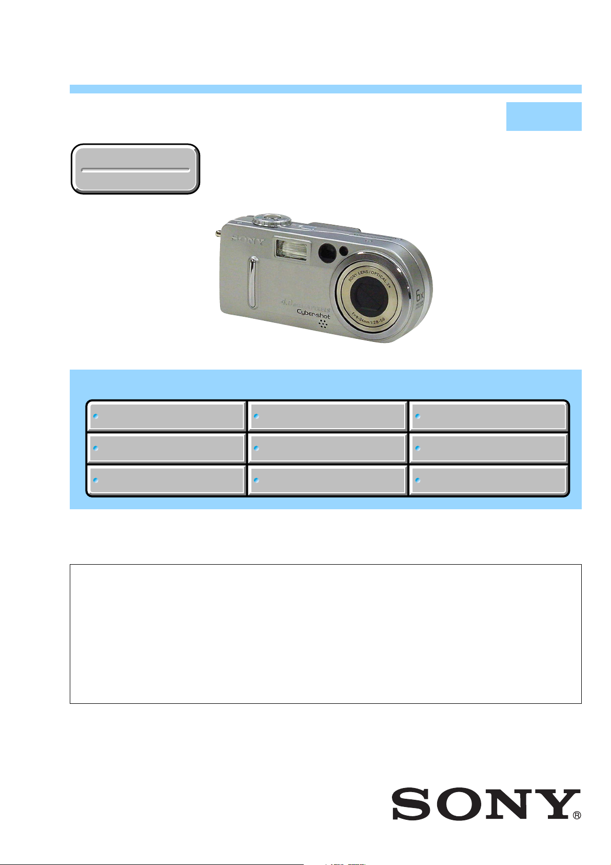
DSC-P9
SERVICE MANUAL
Ver 1.0 2002. 04
Revision History
Revision History
Link
Link
SPECIFICATIONS
SPECIFICATIONS
BLOCK DIAGRAMS
BLOCK DIAGRAMS
LEVEL 2
US Model
Canadian Model
AEP Model
UK Model
E Model
Hong Kong Model
Australian Model
Chinese Model
Korea Model
Tourist Model
Japanese Model
PRINTED WIRING BOARDS
PRINTED WIRING BOARDS
SERVICE NOTE
SERVICE NOTE
DISASSEMBLY
DISASSEMBLY
•For INSTRUCTION MANUAL, refer to SERVICE MANUAL, LEVEL 1 (992997341.pdf).
• This service manual contains information for Japanese model as well.
• Note in Lens Frame Installation.
On the JK-226, JK-227, SY-77 boards
This service manual procides the information that is premised
the circuit board replacement service and not intended repair
inside the JK-226, JK-227, SY-77 boards.
Therefore, schematic diagram, printed wiring board and
electrical parts list of the JK-226, JK-227, SY-77 boards are not
shown.
The following pages are not shown.
FRAME SCHEMATIC DIAGRAMS
FRAME SCHEMATIC DIAGRAMS
SCHEMATIC DIAGRAMS
SCHEMATIC DIAGRAMS
SY-77 board
Schematic diagram ......................... Pages 4-9 to 4-28
Printed wiring board ........................ Pages 4-43 to 4-46
Electrical parts list ........................... Pages 6-9 to 6-13
JK-226, JK-227 boards
Schematic diagram ......................... Pages 4-33 to 4-34
Printed wiring board ........................ Pages 4-49 to 4-50
Electrical parts list ........................... Pages 6-6
The above-described information is shown in service
manual Level 3.
ADJUSTMENTS
ADJUSTMENTS
REPAIR PARTS LIST
REPAIR PARTS LIST
DIGITAL STILL CAMERA
Page 2

DSC-P9
COVER
COVER
SPECIFICATIONS
System
Image device 8.98 mm (1/1.8 type) color
Total pixels number of camera
Lens 3× zoom lens
CCD
Primary color filter
Approx. 4 130 000 pixels
17
/
−
32
15
/16 inches)
−
16
4 19/32 inches))
f=8
24.0 mm (5/
−
(35 mm camera conversion: 39 to
117mm (1
5.6
F2.8
−
Camera
Effective pixels number of camera
Exposure control
White balance
Data formats Movies: MPEG1 (M onaural)
Recording media
Flash Recommended distance
Approx. 3 950 000 pixels
Automatic,
Scene selection (three modes)
Automatic, Daylight, Cloudy,
Fluorescent, Incandescent
Still images: JP EG, GIF (for Clip
Motion)
Audio with still image: MPEG1
(Monaural)
“Memory Stick”
0.5 to 3.8 m (1.6 to 12.5 ft) (W)
0.6 to 2.4 m (2 to 7.9 ft) (T)
(when ISO sens itivity is set to Auto)
Output connectors
A/V OUT (MONO) jack
USB jack mini-B
Minijack
Video: 1 Vp-p, 75
sync negative
Audio: 327 mV (at a 47 k
Output impedance 2.2 k
Ω
, unbalanced,
Ω
load)
Ω
LCD screen
LCD panel used
Total number of do ts
3.8 cm (1.5 type) TFT drive
123 200 (560×220) dots
Power, general
Used battery pack
Power requireme nts
Power consumption (when shooting)
Operating temperature range
Storage temperature range
Dimensions 114 × 51.5 × 35.8 mm
Mass 206 g (7 oz) (NP-FC10 battery pack,
Microphone Electret condenser microphone
Speaker Dynamic speaker
NP-FC10
3.6 V
1.9W
+
40°C (32° to +104°F)
0° to
20° to +60°C (4° to +140°F)
1
/2 × 2 × 1 3/8 inches)
(4
(W/H/D, protruding portions not
included)
“Memory Stick” and wrist strap
included)
AC-LS1A AC power adaptor
Power requirement s
Rated output voltage
Operating temperature range
Storage temperature range
Dimensions 105 × 36 × 56 mm (4
Mass Approx. 180 g (6 oz)
AC 100 – 240 V, 50/60 Hz
DC 4.2 V, 1.5 A
+
40°C (32° to +104°F)
0° to
20° to +60°C (4° to +140°F)
1
/4 inches) (W/H/D, protruding
2
parts not included)
(adaptor only)
1
/4 × 1 7/16 ×
NP-FC10 battery pack
Used battery Lithium ion battery
Maximum voltage
Nominal voltage
Capacity 2.4 Wh (675 mAh)
DC 4.2 V
DC 3.6 V
Accessories
•A/V connecting cable (1)
•NP-FC10 battery pack (1)
•AC-LS1A AC power adaptor (1)
•Power cord (mains lead) (1)
•USB cable (1)
•Wrist strap (1)
•“Memory Stick” (16MB) (1)
•CD-ROM (USB driver: SPVD-008) (1)
•Operating Instructions (1)
Design and specifications are subject to change
without notice.
— 2 —
Page 3

DSC-P9
SAFETY-RELATED COMPONENT WARNING!!
COMPONENTS IDENTIFIED BY MARK 0 OR DOTTED LINE WITH
MARK 0 ON THE SCHEMATIC DIAGRAMS AND IN THE PARTS
LIST ARE CRITICAL TO SAFE OPERATION. REPLACE THESE
COMPONENTS WITH SONY PARTS WHOSE PART NUMBERS
APPEAR AS SHOWN IN THIS MANUAL OR IN SUPPLEMENTS
PUBLISHED BY SONY .
SAFETY CHECK-OUT
After correcting the original service problem, perform the following
safety checks before releasing the set to the customer.
1. Check the area of your repair for unsoldered or poorly-soldered
connections. Check the entire board surface for solder splashes
and bridges.
2. Check the interboard wiring to ensure that no wires are
"pinched" or contact high-wattage resistors.
3. Look for unauthorized replacement parts, particularly
transistors, that were installed during a previous repair. Point
them out to the customer and recommend their replacement.
4. Look for parts which, through functioning, show ob vious signs
of deterioration. Point them out to the customer and
recommend their replacement.
5. Check the B+ voltage to see it is at the values specified.
6. Flexible Circuit Board Repairing
•Keep the temperature of the soldering iron around 270˚C
during repairing.
• Do not touch the soldering iron on the same conductor of the
circuit board (within 3 times).
• Be careful not to apply force on the conductor when soldering
or unsoldering.
ATTENTION AU COMPOSANT AYANT RAPPORT
À LA SÉCURITÉ!
LES COMPOSANTS IDENTIFÉS P AR UNE MARQUE 0 SUR LES
DIAGRAMMES SCHÉMA TIQUES ET LA LISTE DES PIÈCES SONT
CRITIQUES POUR LA SÉCURITÉ DE FONCTIONNEMENT. NE
REMPLACER CES COMPOSANTS QUE PAR DES PIÈSES SONY
DONT LES NUMÉROS SONT DONNÉS DANS CE MANUEL OU
DANS LES SUPPÉMENTS PUBLIÉS PAR SONY.
Unleaded solder
Boards requiring use of unleaded solder are printed with the leadfree mark (LF) indicating the solder contains no lead.
(Caution: Some printed circuit boards may not come printed with
the lead free mark due to their particular size.)
: LEAD FREE MARK
Unleaded solder has the following characteristics.
• Unleaded solder melts at a temperature about 40°C higher than
ordinary solder.
Ordinary soldering irons can be used but the iron tip has to be
applied to the solder joint for a slightly longer time.
Soldering irons using a temperature regulator should be set to
about 350°C.
Caution: The printed pattern (copper foil) may peel away if the
heated tip is applied for too long, so be careful!
• Strong viscosity
Unleaded solder is more viscous (sticky, less prone to flow) than
ordinary solder so use caution not to let solder bridges occur such
as on IC pins, etc.
• Usable with ordinary solder
It is best to use only unleaded solder but unleaded solder may
also be added to ordinary solder.
— 3 —
Page 4

DSC-P9
TABLE OF CONTENTS
Section Title Page Section Title Page
1. SERVICE NOTE ························································1-1
Self-diagnosis Display····················································· 1-3
2. DISASSEMBLY
2-1. BT Lid ·············································································2-2
2-2. Cabinet (Front) Assembly ···············································2-2
2-3. Cabinet (Rear) Assembly················································· 2-3
2-4. LCD Module····································································2-3
2-5. Cabinet (Bottom) Assembly ············································2-4
2-6. Lens Block Assembly······················································2-4
Service Position (SY-77 Board: Side A)··························2-5
2-7. Control Switch Block ······················································2-5
2-8. SY-77 Board ···································································· 2-6
2-9. Memory Stick Connector ················································2-6
2-10. ST-70 Board·····································································2-7
2-11. SW-368 Board ································································· 2-7
2-12. JK-227 Board ··································································2-8
Service Position (SY-77 Board: Side B)··························2-8
2-13. Circuit Boards Location ·················································· 2-9
3. BLOCK DIAGRAMS
3-1. Overall Block Diagram ···················································3-1
3-8. Power Block Diagram 1 ················································3-15
3-9. Power Block Diagram 2 ················································3-17
4. PRINTED WIRING BOARDS AND
SCHEMATIC DIAGRAMS
4-1. Frame Schematic Diagrams·············································4-1
Frame Schematic Diagram (1/2) ·····································4-1
Frame Schematic Diagram (2/2) ·····································4-3
4-2. Schematic Diagrams························································4-5
CD-397 (CCD IMAGER) ···············································4-7
SW-368 (1/2) (CONTROL SWITCH) ··························4-29
SW-368 (2/2)
(LCD DRIVE, TIMING GENERATOR) ·····················4-31
ST-70 (FLASH DRIVE) ···············································4-35
4-3. Printed Wiring Boards ···················································4-39
CD-397 ··········································································4-41
SW-368··········································································4-47
ST-70 ·············································································4-51
4-4. Waveforms·····································································4-54
4-5. Parts Location································································4-57
5. ADJUSTMENTS
Before Starting Adjustment ·······················································5-1
1-1. Adjusting Items when Replacing
Main Parts and Boards ····················································5-2
5-1. Camera Section Adjustments···········································5-3
1-1. Preparations Before Adjustment······································5-3
1-1-1.List of Service Tools ························································5-3
1-1-2.Preparations ·····································································5-4
1-1-3.Discharging of the Flashlight Power Supply··················· 5-4
1-1-4.Precautions ······································································5-6
1. Setting the Switch···························································· 5-6
2. Order of Adjustments ······················································5-6
3. Subjects ···········································································5-6
4. Preparing the Flash Adjustment Box·······························5-7
1-2. Initialization of A, B, D, E, F, 7, 9 Page Data ················· 5-8
1-2-1.Initialization of A, D Page Data ······································ 5-8
1. Initializing A, D Page Data ··············································5-8
2. Modification of A, D Page Data ······································ 5-8
3. A Page Table····································································5-8
4. D Page Table····································································5-8
1-2-2.Initialization of B, E, F, 7, 9 Page Data ···························5-9
1. Initializing B, E, F, 7, 9 Page Data ··································5-9
2. Modification of B, E, F, 7, 9 Page Data.··························5-9
3. B Page Table ····································································5-9
4. E Page Table ····································································5-9
5. F Page Table ··································································5-10
6. 7 Page Table···································································5-12
7. 9 Page Table···································································5-12
1-3. Video System Adjustments············································ 5-13
1. Video Sync Level Adjustment ·······································5-13
2. Video Burst Level Check···············································5-13
1-4. Camera System Adjustments·········································5-14
Data Setting During Camera System Adjustments········5-14
Picture Frame Setting ····················································5-15
Check on the Oscilloscope ············································5-15
1. Flange Back Adjustment
(Using the minipattern box) ··········································5-16
2. Flange Back Adjustment
(Using the flange back adjustment chart)······················5-17
3. Flange Back Check························································ 5-17
4. F No. Compensation ······················································ 5-18
5. Mechanical Shutter Adjustment ····································5-18
6. Light V alue Adjustment ·················································5-19
7. Mixed Color Cancel Adjustment··································· 5-19
8. Auto White Balance 3200K Standard Data Input 1 ······5-20
9. Auto White Balance 3200K Standard Data Input 2 ······5-21
10. Auto White Balance 3200K Standard Data Input 3 ······ 5-21
11. Auto White Balance 3200K Check ·······························5-22
12. Auto White Balance 5800K Standard Data Input 1 ······ 5-23
13. Auto White Balance 5800K Standard Data Input 2 ······ 5-24
14. Auto White Balance 5800K Standard Data Input 3 ······ 5-24
15. Auto White Balance 5800K Check ·······························5-25
16. CCD Linearity Check ····················································5-26
17. Color Reproduction Adjustment····································5-27
18. CCD White Defect Compensation ································5-28
19. CCD Black Defect Compensation·································5-29
20. Strobe White Balance Adjustment·································5-30
21. AF Illumination Check ··················································5-32
1-5. LCD System Adjustments ·············································5-33
1. LCD Initial Data Input ··················································5-34
2. VCO Adjustment (SW-368 Board)································5-34
3. Black Limit Adjustment (SW-368 Board) ·····················5-35
4. Bright Adjustment (SW-368 Board) ······························5-35
5. Contrast Adjustment (SW-368 Board) ··························5-36
6. VG Center Adjustment (SW-368 Board)·······················5-36
7. PSIG Gray Adjustment (SW-368 Board) ······················5-37
8. V-COM Adjustment (SW-368 Board) ··························· 5-37
9. White Balance Adjustment (SW-368 Board) ················5-38
5-2. Service Mode·································································5-39
2-1. Adjusting Remote Commander ·····································5-39
1. Used the Adjusting Remote Commander ······················5-39
2. Precautions upon Using the Adjusting
Remote Commander······················································5-39
2-2. Data Process ··································································5-40
2-3. Service Mode·································································5-41
1. Setting the Test Mode ····················································5-41
2. Bit V alue Discrimination ···············································5-41
3. Mode Dial Check (1) ·····················································5-41
4. Mode Dial Check (2) ·····················································5-41
5. Switch Check (1) ···························································5-41
6. Switch Check (2) ···························································5-42
7. LED Check ····································································5-42
8. Self Diagnosis Code ······················································5-42
— 4 —
Page 5

Section Title Page
6. REPAIR PARTS LIST
6-1. Exploded Vie ws ·······························································6-1
6-1-1.Cabinet (Front) Section ···················································6-1
6-1-2.Cabinet (Rear) Assembly·················································6-2
6-1-3.Lens Block and LCD Section ··········································6-3
6-1-4.Battery Holder Assembly ················································6-4
6-2. Electrical Parts List ·························································6-5
* The color reproduction frame is shown on page 113.
DSC-P9
— 5 —
Page 6
DSC-P9
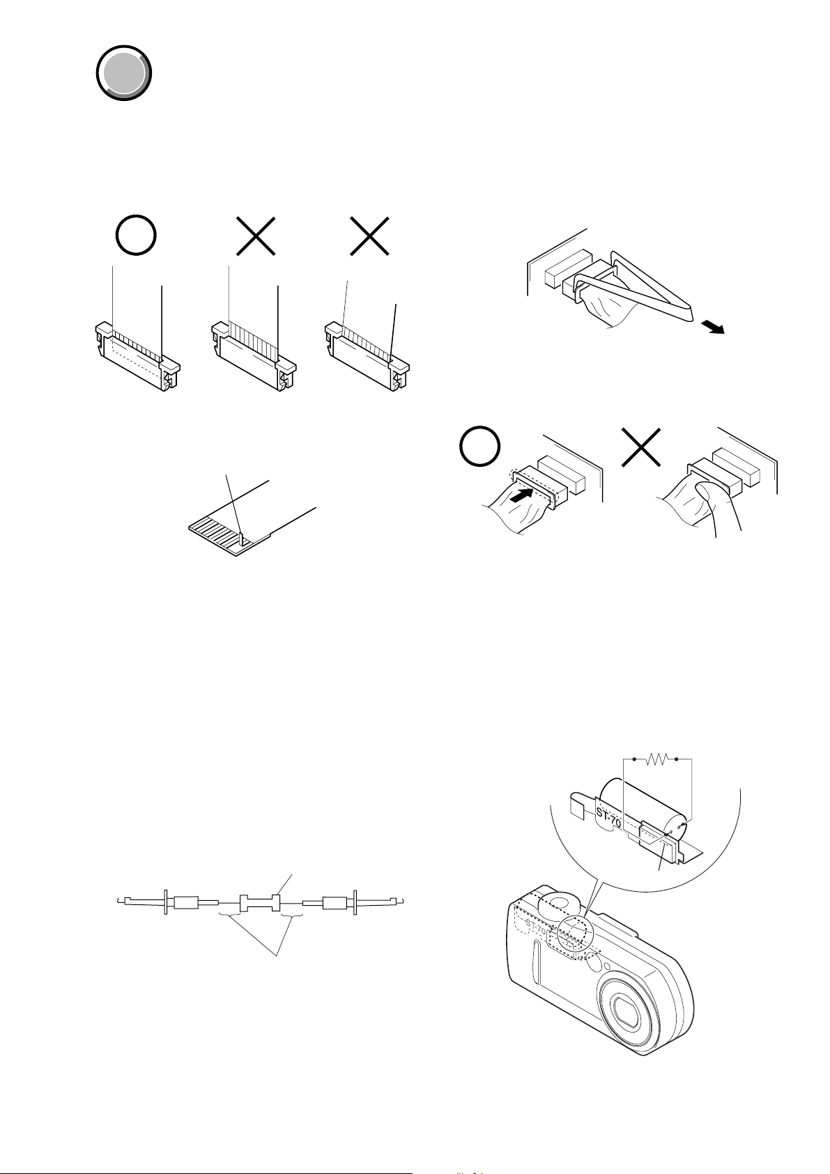
When installing a connector, don’t press down at wire of connector.
It is possible that a wire is snapped.
COVER
COVER
SECTION 1
SERVICE NOTE
• NOTE FOR REPAIR
Make sure that the flat cable and flexible board are not cracked of
bent at the terminal.
Do not insert the cable insufficiently nor crookedly.
Cut and remove the part of gilt
which comes off at the point.
(Be careful or some
pieces of gilt may be left inside)
When remove a connector, don’t pull at wire of connector.
It is possible that a wire is snapped.
[Discharging of the ST-70 flexible board’s charging
capacitor (C510)]
The charging capacitor (C003) of the ST -70 flexible board is char ged
up to the maximum 300 V potential.
There is a danger of electric shock by this high voltage when the
battery is handled by hand. The electric shock is caused by the
charged voltage which is kept without discharging when the main
power of the unit is simply turned off. Therefore, the remaining
voltage must be discharged as described below.
Preparing the Short Jig
To preparing the short jig, a small clip is attached to each end of a
resistor of 1 kΩ /1 W (1-215-869-11).
Wrap insulating tape fully around the leads of the resistor to prevent
electrical shock.
1 kΩ/1 W
Wrap insulating tape.
Discharging the Capacitor
Short-circuit between the positive and the negative terminals of
charged capacitor with the short jig about 10 seconds.
R:1 kΩ/1 W
(Part code:
1-215-869-11)
Capacitor
1-1
Page 7

DSC-P9
[Precaution on Replacing the Video Lens or the SY-77
Board]
The DSC-P9 uses the position sensor to detect the zoom position.
Accordingly, the zoom position will v ary if the position data changes
due to the replacement of the video lens or the SY-77 board, thus
causing the video lens to collide against the mechanism end when
the power is turned off.
Though the position data is calibrated at the “Flange Back
Adjustment”, add the following work when making an adjustment
at the replacement of video lens to prevent a collision of video lens.
When Replacing the Video Lens
1) With current video lens assembled, turn the power on, and set
the bit value of Bit0 on Page:9, Address:17 to “0” using the
adjusting remote commander, then turn the power off.
2) Replace the video lens with a new one, turn the power on, and
perform the “Flange Back Adjustment”.
Thus, new position data will be written.
3) After the “Flange Back Adjustment”, return the bit value of Bit0
on Page:9, Address:17 to “1” using the adjusting remote
commander.
When Replacing the SY-77 Board
1) Replace the SY-77 board with a new one, set the mode dial to
“PLAY”, turn the power on, and set the bit value of Bit0 on
Page:9, Address:17 to “0” using the adjusting remote
commander, then turn the power off.
2) Set the mode dial to “CAMERA”, turn the power on, and
perform the “Flange Back Adjustment”.
Thus, new position data will be written.
3) After the “Flange Back Adjustment”, return the bit value of Bit0
on Page:9, Address:17 to “1” using the adjusting remote
commander.
[Note in Lens Frame Installation]
When tightening a screw , have both sides of the lens b lock assemb ly
so as not for the load to depend.
M1.7 × 4
Lens block assembly
Lens frame
M1.7 × 4
1-2
Page 8
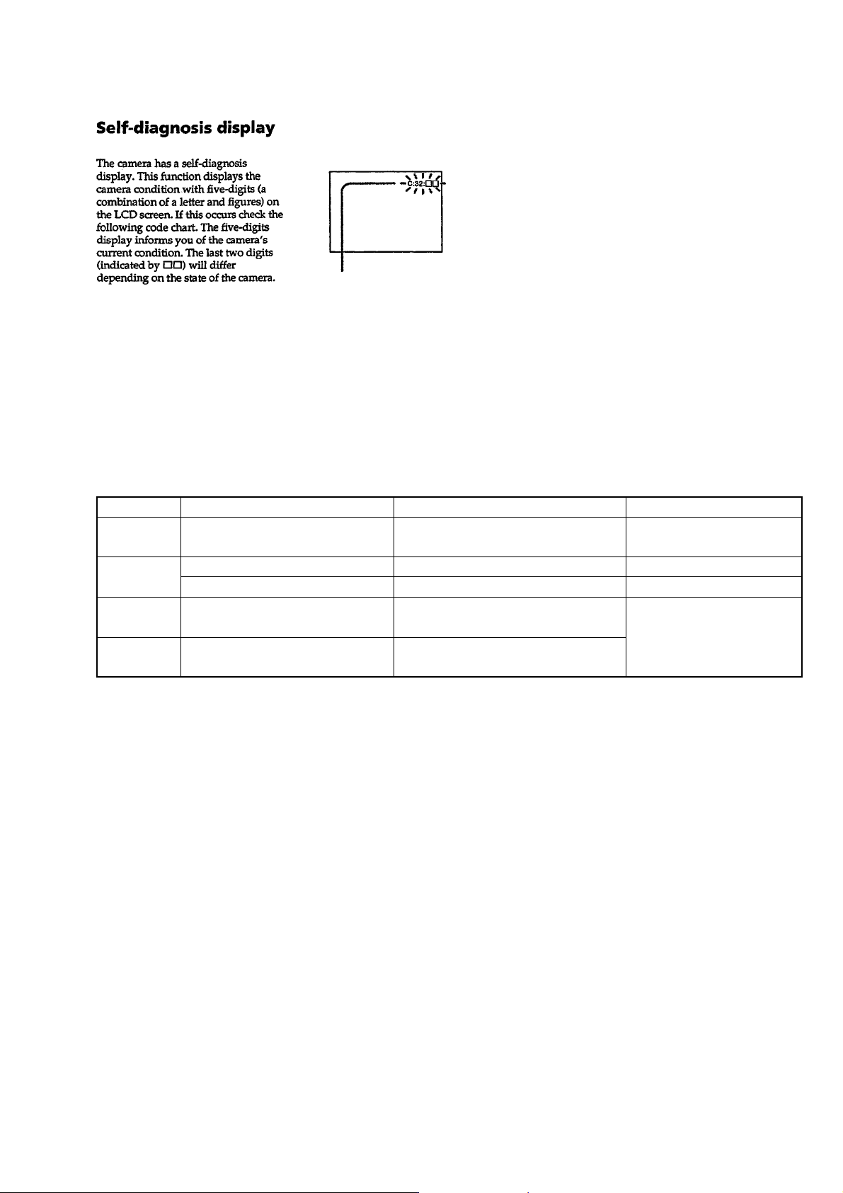
[Description on Self-diagnosis Display]
Self-diagnosis display
• C: ss: ss
You can reverse the camera
malfunction yourself. (However,
contact your Sony dealer or local
authorized Sony service facility
when you cannot recover from the
camera malfunction.)
• E: ss: ss
Contact your Sony dealer or local
authorized Sony service facility.
DSC-P9
Display Code
C:32:ss
C:13:ss
E:61:ss
E:91:ss
Countermeasure
Turn the power off and on again.
Format the “Memory stick”.
Insert a new “Memory Stick”.
Checking of lens drive circuit.
Checking of flash unit or replacement
of flash unit.
Cause
Trouble with hardware.
Unformatted memory stick is inserted.
Memory stick is broken.
When failed in the focus and zoom
initialization.
Abnormality when flash is being
charged.
Caution Display During Error
SYSTEM ERROR
FORMAT ERROR
MEMORY STICK ERROR
—
1-3E
Page 9
DSC-P9
COVER
COVER
• This set can be disassembled in the order shown below.
DSC-P9
2-2. CABINET (FRONT)
ASSEMBLY (Page 2-2)
2-7. CONTROL SWITCH
BLOCK (Page 2-5)
2-1. BT LID
(Page 2-2)
2-3. CABINET (REAR)
ASSEMBLY (Page 2-3)
2-5. CABINET (BOTTOM)
ASSEMBLY (Page 2-4)
2-6. LENS BLOCK ASSEMBLY
(Page 2-4)
SECTION 2
DISASSEMBLY
2-4. LCD MODULE
(Page 2-3)
SERVICE POSITION
(SY-77 BOARD: side A)
(Page 2-5)
2-8. SY-77 BOARD
(Page 2-6)
2-9. MEMORY STICK
CONNECTOR (Page 2-6)
2-11. SW-368 BOARD
(Page 2-7)
2-12. JK-227 BOARD
(Page 2-8)
2-10. ST-70 BOARD
(Page 2-7)
SERVICE POSITION
(SY-77 BOARD: side B)
(Page 2-8)
2-1
Page 10
DSC-P9
Note: Follow the disassembly procedure in the numerical order given.
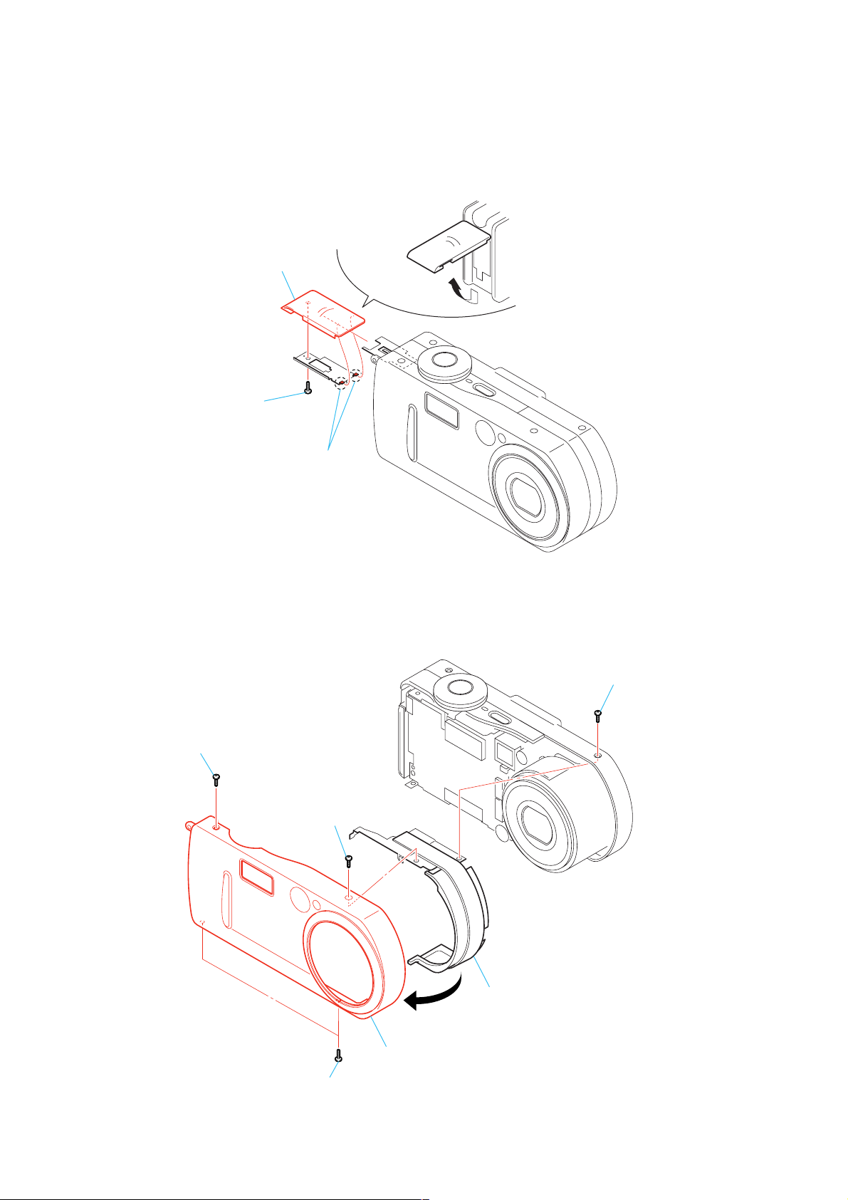
2-1. BT LID
1 Open the BT lid.
4 BT lid
2 Screw
(1.7 × 3)
3 Two claws
2-2. CABINET (FRONT) ASSEMBLY
1 Screw
(M1.7)
2 Screw
(M1.7)
6 Screw
(M1.7)
3 Two screws
(M1.7)
7 Center cabinet
4
5 Cabinet (front)
assembly
2-2
Page 11
2-3. CABINET (REAR) ASSEMBLY
DSC-P9
2 Screw
(M1.7)
5 Cabinet (rear)
assembly
1 Screw
(M1.7)
4
3 Two screws
(M1.7)
2-4. LCD MODULE
1 Flexible board
(CN102)
6 LCD module
2 Flexible board
(CN101)
3 Two screws
(M1.7)
4 Four claws
5 Back light unit
2-3
Page 12
DSC-P9
2-5. CABINET (BOTTOM) ASSEMBLY
1 Claw
Rear side
2 Cabinet (bottom) assembly
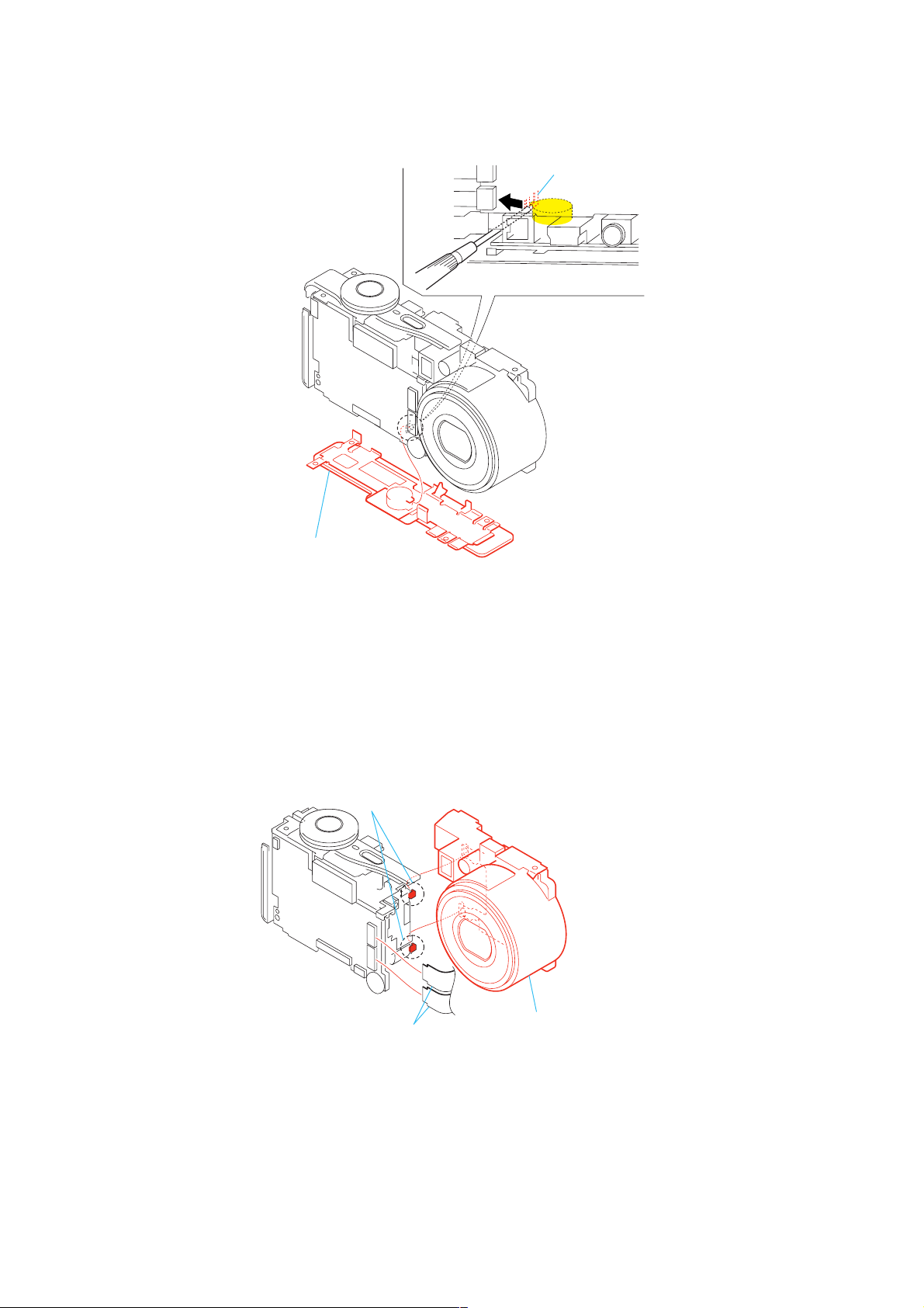
2-6. LENS BLOCK ASSEMBLY
2 Two claws
1 Two flexible board
(CN001, 301)
3 Lens block assembly
2-4
Page 13
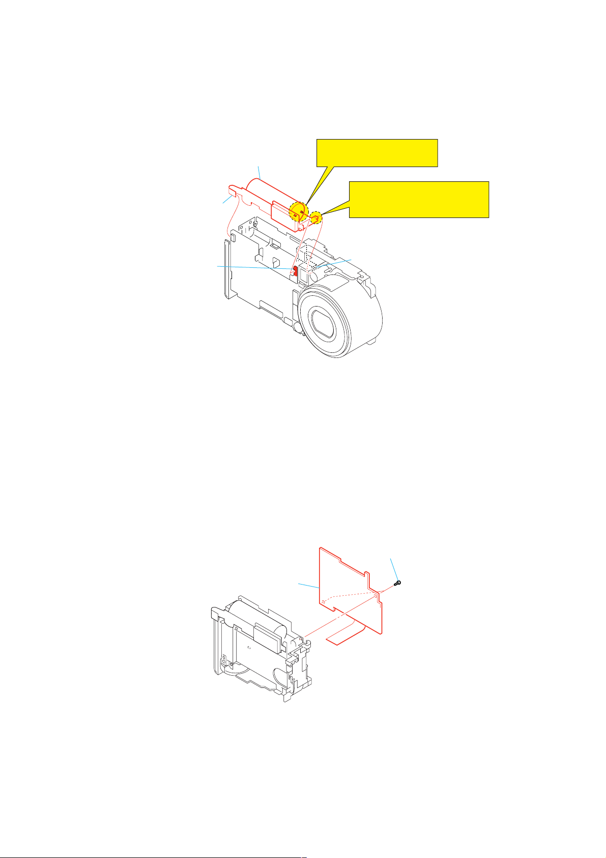
[SERVICE POSITION (SY-77 BOARD: SIDE A)]
DSC-P9
CPC-9 jig
(J-6082-393-C)
Regulated power supply
(6.0 to 7.2 Vdc)
Note 1: Don’t use the 12 pin flexible board of CPC-9 jig.
Note 2: The old CPC-9 jig (Parts code: J-6082-393-B)
Adjusting remote
commander
SY-77 board
18
1
Color monitor
LCD module
Back light unit
18
1
It causes damage to the unit.
cannot be used, because it cannot operate
the adjustment remote commander.
Lens block assembly
Base
AC power
adaptor
AC IN
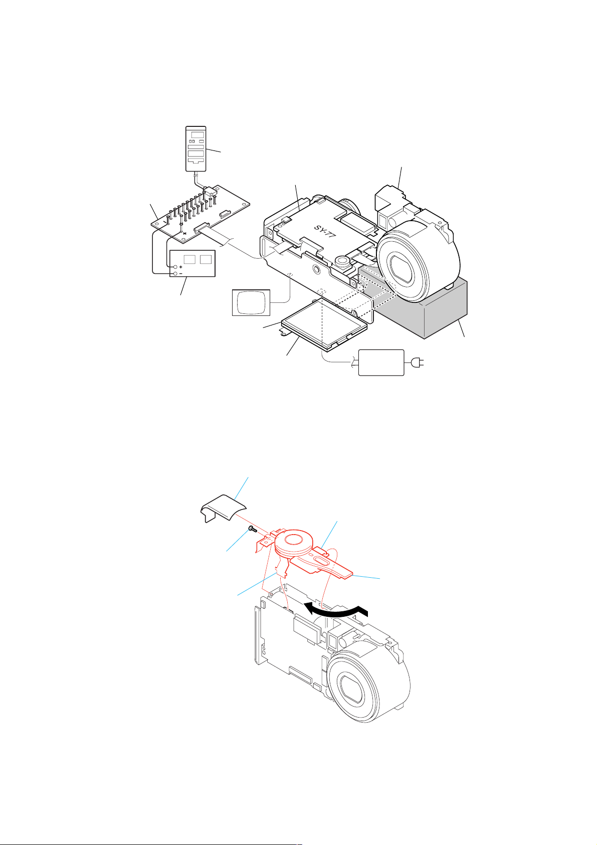
2-7. CONTROL SWITCH BLOCK
1 Mode dial cover
2 Screw
(M1.7)
5 Flexible board
(CN704)
3 Claw
6 Control swith block
4
2-5
Page 14
DSC-P9
2-8. SY-77 BOARD
5 Claw
1 Connector
(CN351)
7 SY-77 board
4 Screw
(M1.7 × 4)
2 Flexible board
(CN703)
6 Flexible board
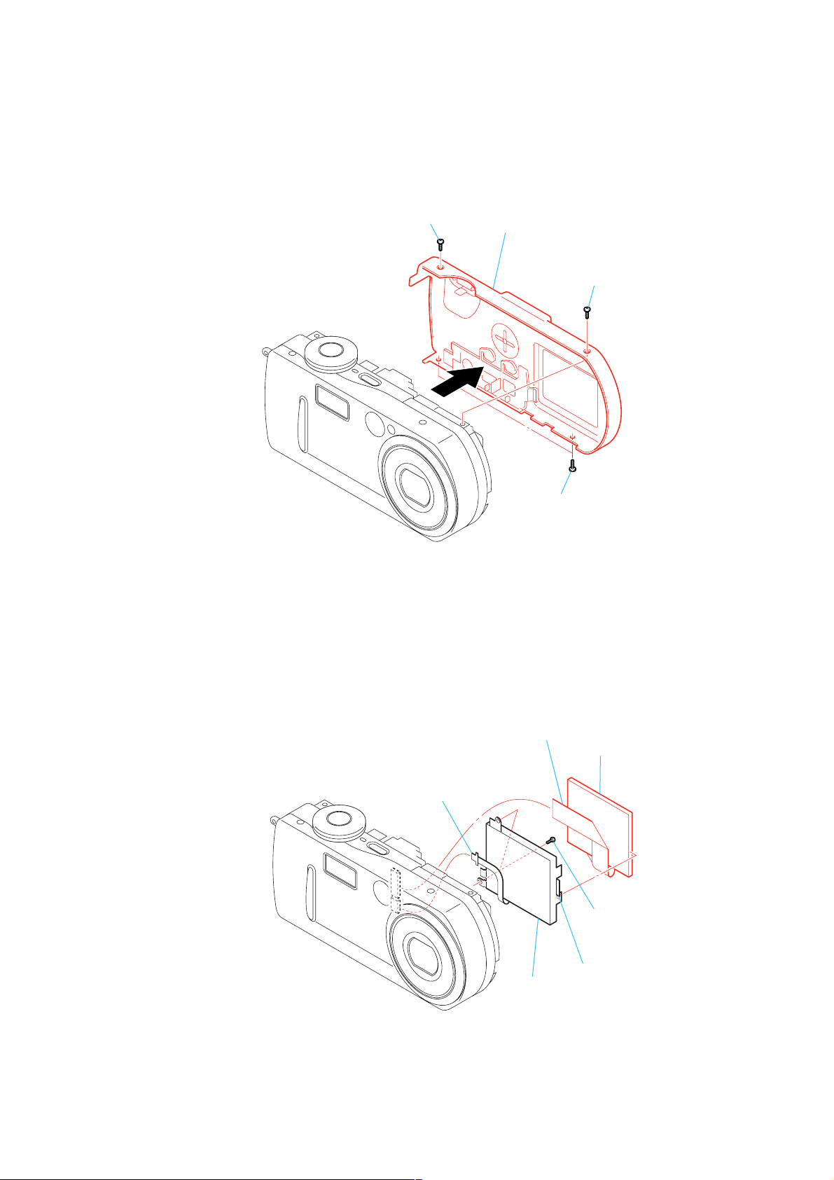
2-9. MEMORY STICK CONNECTOR
1 Two screws
(M1.7 × 4)
(CN701)
3 Three flexible boards
(CN001, 301, 702)
2 Claw
3 Memory stick connector
2-6
Page 15
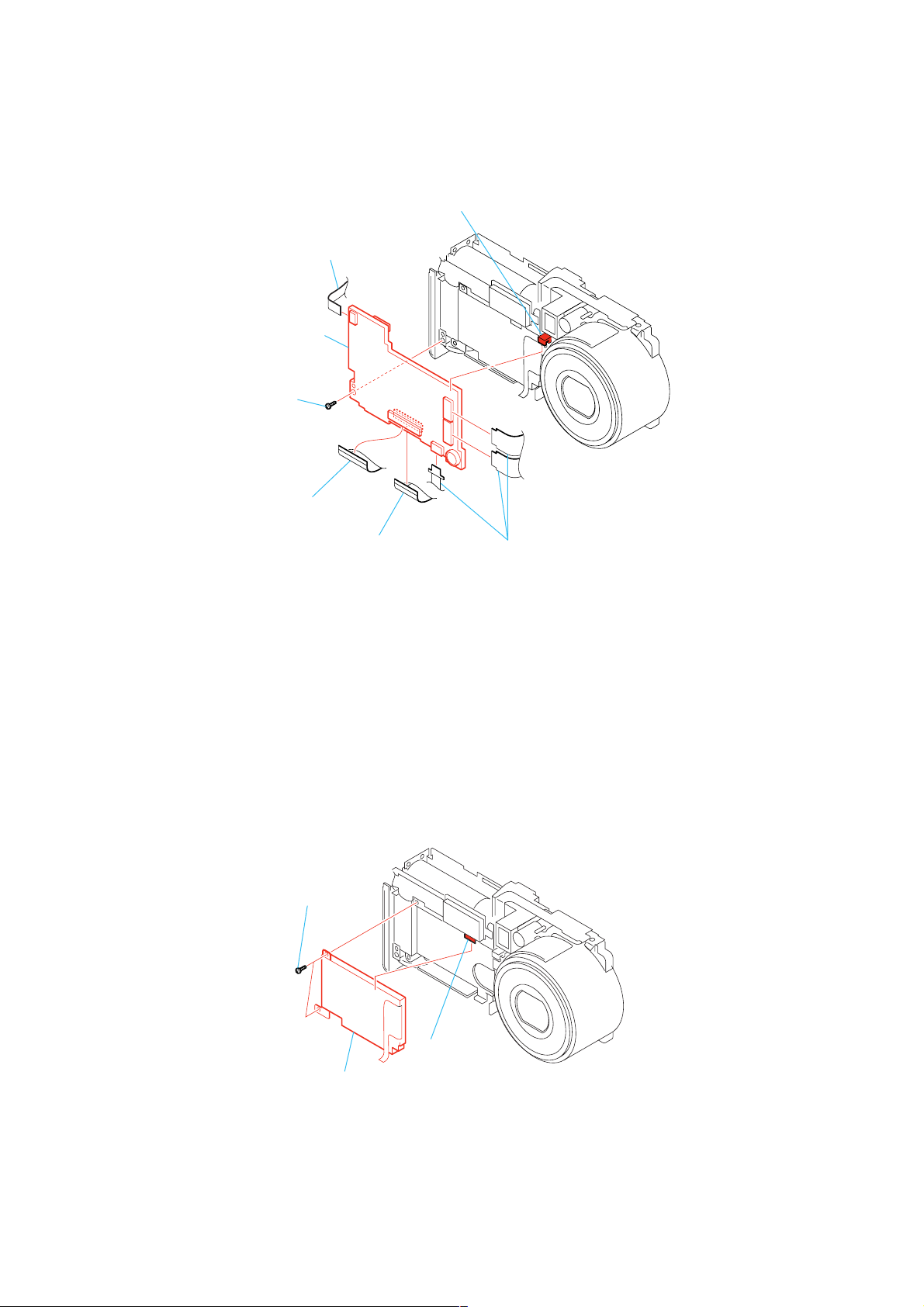
2-10.ST-70 BOARD
1 Connector
(CN351)
3 ST-70 board
DSC-P9
Note: High-voltage cautions
(See page 1-1).
Note: When installing ST-70 board,
the claw is put into the bottom
the BT main frame.
2-11.SW-368 BOARD
2 Claw
BT main frame
1 Two screws
(M1.7 × 4)
2 SW-368 board
2-7
Page 16
DSC-P9
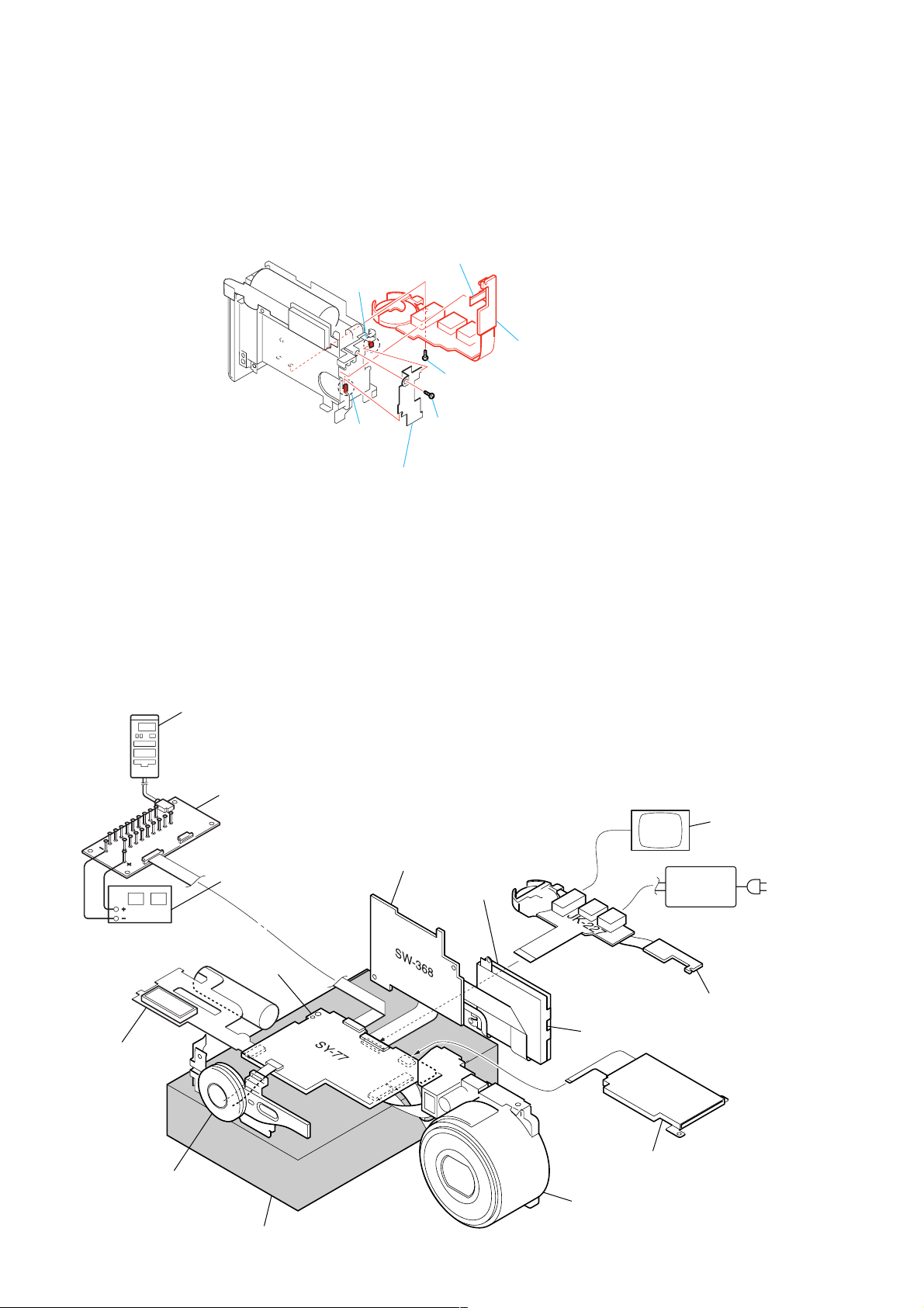
2-12.JK-227 BOARD
6 Claw
2 Claw
7 JK-227 board
(including JK-226)
5 Screw
(M1.7)
3 Claw
4 DD sheet metal
1 Screw
(M1.7 × 4)
[SERVICE POSITION (SY-77 BOARD: SIDE B)]
Adjusting remote
commander
CPC-9 jig
(J-6082-393-C)
18
1
Regulated power supply
(6.0 to 7.2 Vdc)
Note 1: Don’t use the 12 pin flexible board of CPC-9 jig.
It causes damage to the unit.
Note 2: The old CPC-9 jig (Parts code: J-6082-393-B)
cannot be used, because it cannot operate
the adjustment remote commander.
SW-368 board
LCD module
Color monitor
AC power
adaptor
AC IN
ST-70 board
Mode dial block assembly
SY-77 board
Base
18
JK-227 board
1
Back light unit
Memory stick connector
Lens block assembly
2-8
Page 17
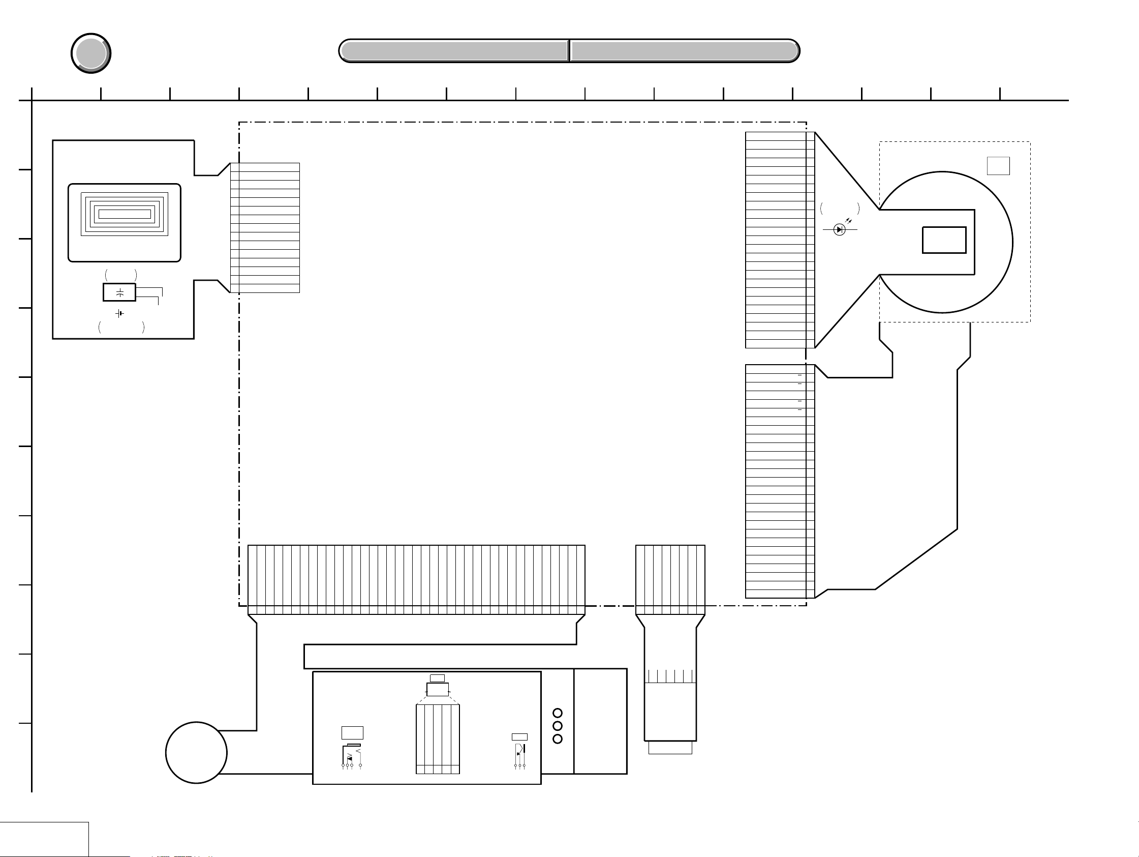
2-13.CIRCUIT BOARDS LOCATION
SW-368
SY-77
DSC-P9
ST-70
CD-397
JK-227
(including JK-226)
Board Name Function
CD-397 CCD IMAGER
SY-77 CAMERA MODULE, CAMERA DSP, VIDEO, MEMORY,
LENS DRIVE, SH DSP, FLASH MEMORY, FRONT CONTROL,
AUDIO, CLOCK GENERATOR, FLASH CONTROL,
DC/DC CONVERTER, CAMERA PROCESS
ST-70 FLASH DRIVE
SW-368 CONTROL SWITCH, LCD DRIVE, TIMING GENERATOR
JK-227 JACK
(including JK-226)
2-9E
Page 18

COVER
COVER
3. BLOCK DIAGRAMS
Link
Link
OVERALL BLOCK DIAGRAM POWER BLOCK DIAGRAM 2
OVERALL BLOCK DIAGRAM POWER BLOCK DIAGRAM 2
POWER BLOCK DIAGRAM 1
POWER BLOCK DIAGRAM 1
DSC-P9
Page 19
DSC-P9
COVER
COVER
BLOCK DIAGRAMS
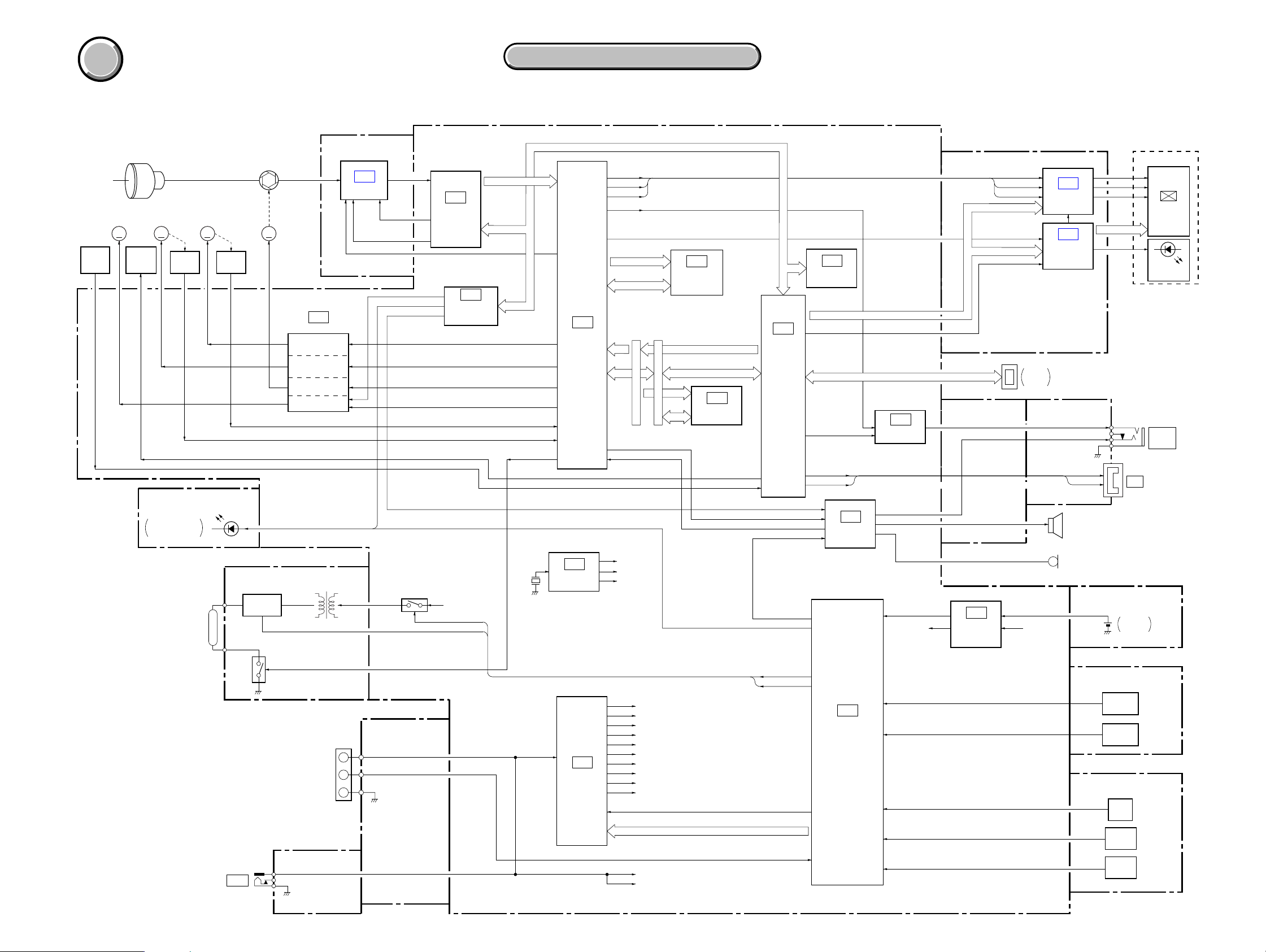
3-1. OVERALL BLOCK DIAGRAM
LENS
TEMP
SENSOR
SHUTTER
MOTOR
LENS
ZOOM
MOTOR
MM
ZOOM
POSITION
SENSOR
SENSOR
CD-397 BOARD (2/2)
D101
SELF TIMER/
AF ILLUMINATOR
ZOOM
FOCUS
MOTOR
M
FOCUS
SENSOR
IRIS
MOTOR
IRIS
METER
M
SECTION 3
3. BLOCK DIAGRAMS
3. BLOCK DIAGRAMS
( ) : Number in parenthesis ( ) indicates the division number of schematic diagram where the component is located.
CCD OUT
SY-77 BOARD
IC151
CAMERA
MODULE
(1/10)
(D/A CONVERTER)
ZOOM POS
LENS TEMP
SELF TIMER LED
DATA BUS 14
IC508
EVR
(6/10)
HR DIR0A, HR DIR0B, HR EN0
HR DIR1A, HR DIR1B, HR EN1
IRIS M IN, IRIS M EN,
IRIS S IN, IRIS S EN
MSHUT ON
MSHUT EN
XFC RST SENS
XZM RST SENS
STRB ON
CAM SO, XCAM SCK
IC601
CAMERA
DSP
(2/10)
PANEL R
PANEL G
PANEL B
CV OUT
ADDRESS BUS14
DATA BUS 32
25
16
ADDRESS BUS
AU AINL
AU AOUT
25
16
20
DATA BUS
16
IC602
256M
SDRAM
(3/10)
IC504
16M FLASH
(6/10)
ZOOM POS
LENS TEMP
IC501
MC CAM,
SH DSP
(5/10)
BEEP, BEEP ON
CD-397 BOARD (1/2)
IC302
(4/10)
FOCUS MOTOR
DRIVER
ZOOM MOTOR
DRIVER
IRIS
DRIVER
SHUTTER DRIVER
IC101
CCD IMAGER
V1A, V1B, V2
V3A, V3B, V4
VSUB CONT
H1, H2
PRELAMP AF ON
CAM SO, XCAM SCK
SP VOL
AU AINL
AU AOUT
IC505
EEPROM
(6/10)
VAMP ON
USB D+
USB D
LCD SO, XLCD SCK
CV OUT
−
IC201
AUDIO AMP
(8/10)
MS DIO, MS BS, MS SCLK
IC101
VIDEO AMP
(3/10)
SW-368 BOARD (1/2)
PANEL R
PANEL G
PANEL B
LCD SO, XLCD SCK
V OUT
AU OUT
MS
SOCKET
JK-226 BOARD (2/2)JK-227 BOARD (2/2)
IC101
LCD DRIVE
(2/2)
IC102
LCD TIMING
GENERATOR
(2/2)
USB D+
USB D–
SP901
SPEAKER
PANEL UNIT
VR
VG
VB
CN002
USB
LCD901
COLOR
LCD
MONITOR
D901
BACK LIGHT
J002
A/V OUT
(MONO)
FLASH
UNIT
ST-70 BOARD (1/2)
CHARGING
CAPACITOR
Q002
J001
DC IN
JK-226 BOARD (1/2)
T001
BT901
BATTERY
TERMINAL
JK-227 BOARD (1/2)
+
S
–
Q360, 361
ACV UNREG
STB CHARGE
XSTB FULL
X501
27MHz
IC507
CLOCK GEN.
(6/10)
IC001
DC/DC
CONTROL
(10/10)
TG CLK
USB CLK
MC CLK
CAM 15V
CAM 3.2V
CAM –7.5V
A 4.9V
A 2.9V
D 1.5V
D 2.9V
PANEL 2.9V
BL VO–
FR 5V
AVC UNREG
BATT UNREG
UNREG SCK, UNREG SO
BEEP, BEEP ON
SELF TIMER LED
STB CHG
XSTB FULL
SYS DD ON
BATT SIG
IC401
FRONT CONTROLLER
(7/10)
RESET
KEY AD0, 1
KEY AD3
MODE DIAL, XPB ON, XSET UP ON
XPWR ON
XAE LOCK SW, XSHTR ON
IC403
INITIAL RESET,
BACK UP VCC
(7/10)
MIC901
MICROPHONE
ST-70 BOARD (2/2)
BT001
LITHIUM
FR 5VEVER 3.0V
BATTERY
SW-368 BOARD (2/2)
FUNCTION
SWITCH
ZOOM
SWITCH
CONTROL SWITCH BLOCK
MODE
DIAL
POWER
ON/OFF
SHUTTER
SWITCH
05
3-1 3-2
Page 20
DSC-P9
COVER
COVER
3. BLOCK DIAGRAMS
3. BLOCK DIAGRAMS
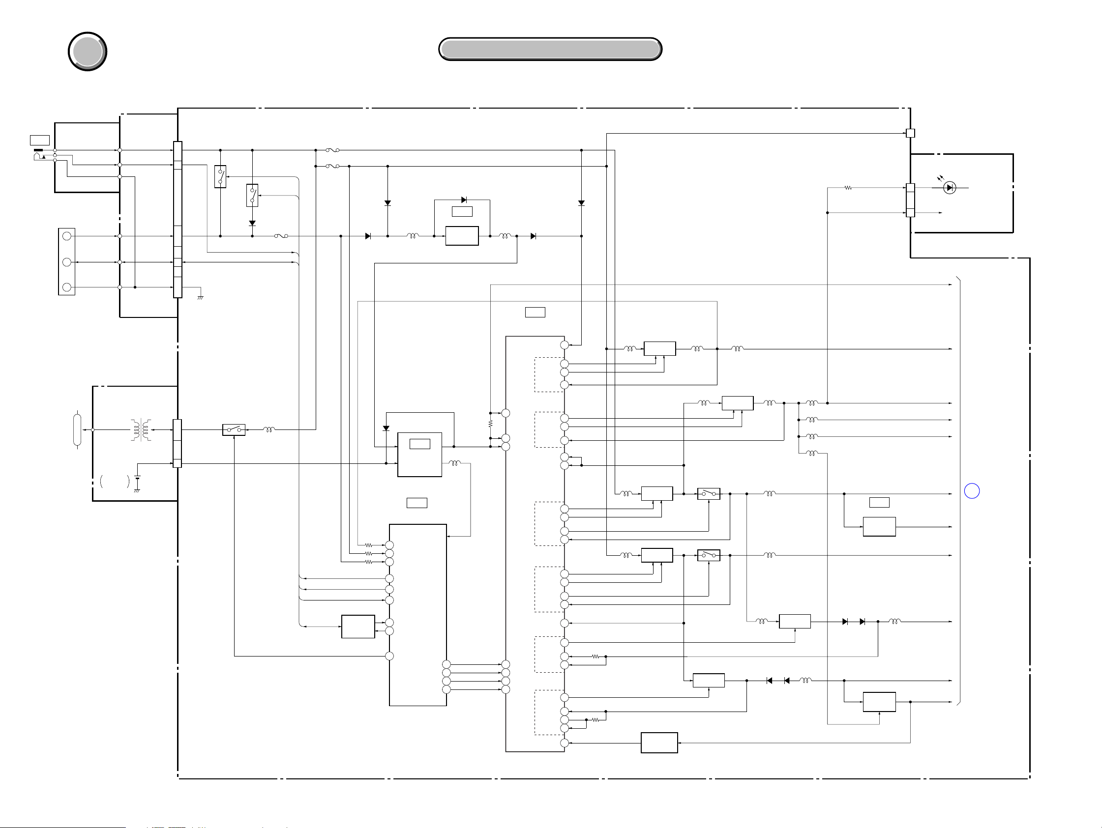
3-8. POWER BLOCK DIAGRAM 1
SY-77 BOARD (1/2)
CN703
17
ı
24
37
1
ı
8
36
9
ı
16
CN351
4
ST UNREG
ı
8
VL 3V
1
J001
DC IN
BT901
BATTERY
TERMINAL
JK-226 BOARD
ACV UNREG
BATT/XEXT
BATT UNREG1
+
BATT SIG
S
BATT GND
–
FLASH
UNIT
GND
ST-70 BOARD
BT001
LITHIUM
BATTERY
JK-227 BOARD
ACV UNREG1
BATT/XEXT
BATT
UNREG1
BATT SIG
GND
T001
( ) : Number in parenthesis ( ) indicates the division number of schematic diagram where the component is located.
F004
Q017, 018
Q015, 021
CHARGE
CONTROL
Q360, 361
FAST CHARGE
INIT CHARGE
D008
F001
BATT/XEXT
BATT SIG
L351
STB CHARGE
F003
FAST CHARGE
INIT CHARGE
BATT/EXT
BATT SIG
D009
D007 D001
D006
Q408
BATTERY
CHARGE
DETECTOR
L016
FR 5V
DD CON SENS
D407
IC403
INITIAL RESET,
BACK UP VCC
(7/10)
IC404
FRONT CONTROLLER
(7/10)
66 DD CON SENS
68
ACV SENS
67 BATT SENS
48
FAST CHARGE
INIT CHARGE
47
8
BATT/XEXT
BATT SI
43
BATT SO
42
46 STB CHG
SYS DD ON
XCS DDCON
UNREG SO
UNREG SCK
IC002
(10/10)
DC/DC
CONVERTER
EVER 3.0V
L401
SYS DD ON
76
XCS DDCON
22
UNREG SO
20
UNREG SCK
21
L017
DC/DC CONTROL
47
RST
48
LD ON
56
VCC1
57
CONT
44
XCS
45
DATA
46
CLK
D010
IC001
(10/10)
AMP OUT
VCC2
OUT 1p
OUT 1n
VIN 1–
OUT 4p
OUT 4n
VIN 4–
VCC3
VCC5
OUT 5p
OUT 5n
OUT 5S
VIN 5–
OUT 6p
OUT 6n
OUT 6S
VIN 6–
VCC4
OUT 9
IN 9–
SCP 9
OUT 10
AMP IN
IN 10
SCPIN
41
36
37
55
30
31
53
42
20
38
39
43
52
28
29
18
50
19
23
80
1
22
4
5
−
3
10
L004
L002
SWITCHING
Q008, 010
SWITCHING
Q009, 011
SWITCHING
EMERGENCY
Q002, 005
Q001
DETECT
L005L019 L011
Q003, 006
L020
SWITCHING
Q012
Q013
Q004
SWITCHING
L006
L012
L013
L001
D004 D005
Q007
SWITCHING
L010
L007
L008
L009
L021
D002 D013
CN706
HI UNREG
CN704
PWR LED VCC
D 2.9V
IC003
(10/10)
3.2V
REG
L014
Q019, 020
–7.5V
REG
CPC
10
(FOR CHECK)
CONTROL SWITCH BLOCK
12
3
EVER 3.0V
D 1.5V
D 2.9V
A 2.9V
PANEL 2.9V
A 4.9V
CAM 3.2V
M 5V
CAM 15V
BL VO–
CAM –7.5V
D 2.9V
A
(POWER)
POWER 2
(PAGE 3-17)
05
3-15 3-16
Page 21
COVER
COVER
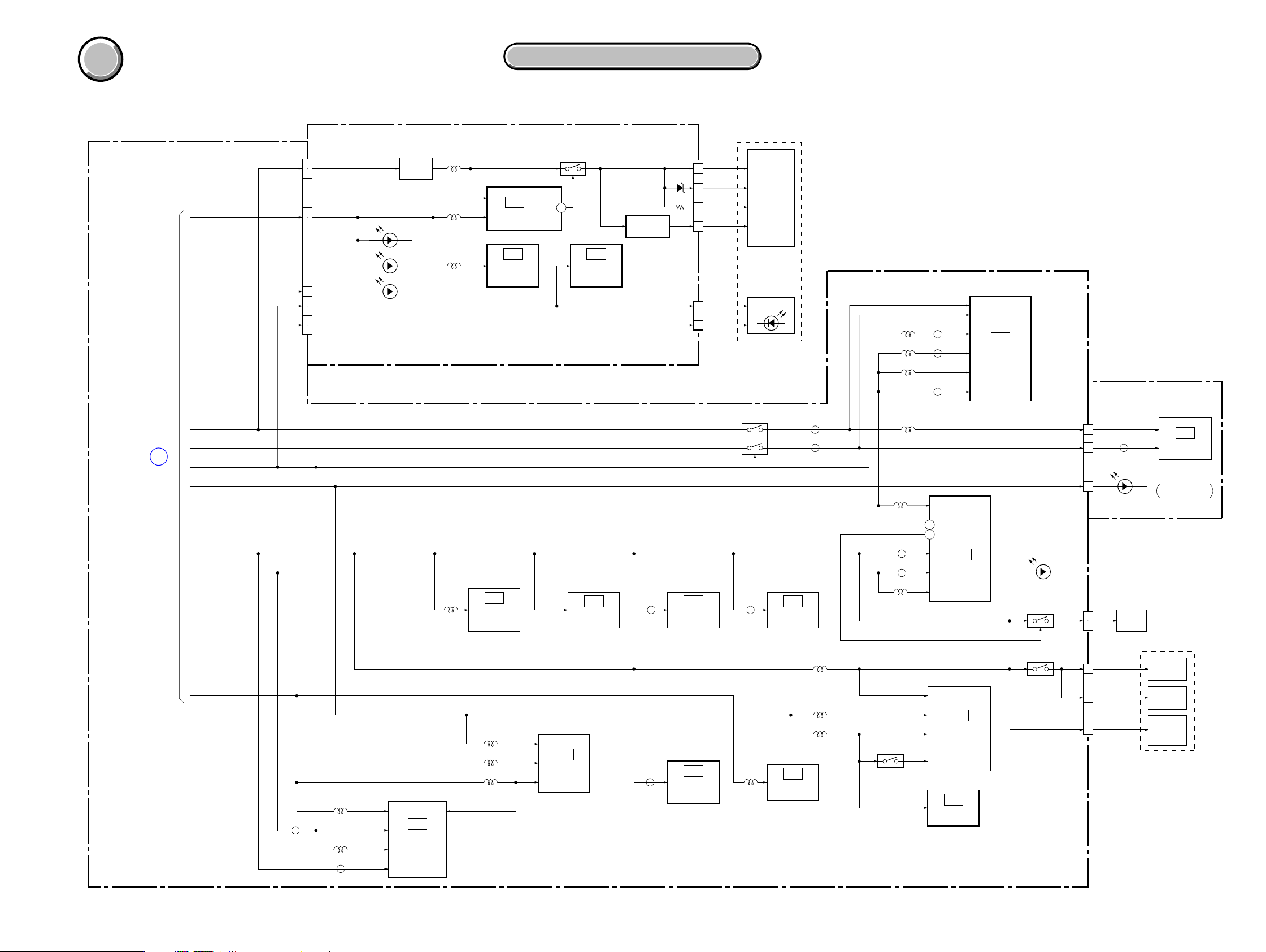
3. BLOCK DIAGRAMS
3. BLOCK DIAGRAMS
DSC-P9
3-9. POWER BLOCK DIAGRAM 2
SY-77 BOARD (2/2)
POWER 1
(PAGE 3-16)
PANEL 2.9V
EVER 3.0V
BL VO–
CAM 15V
CAM −7.5V
A
A 4.9V
M 5V
CAM 3.2V
D 2.9V
D 1.5V
CN701
( ) : Number in parenthesis ( ) indicates the division number of schematic diagram where the component is located.
SW-368 BOARD
CAM15V
32
33
PANEL 2.9V
11
12
EVER 3.0V
3
A 4.9V
30
31
BL VO–
1
2
Q002, 003
13.5V
REG
D003
(AE LOCK)
D004
(TALLY)
D002
(FLASH/CHG)
L102
L101
L104
L503
LCD DRIVER
LCD TIMING
GENERATOR
IC508
EVR
(D/A CONV.)
(6/10)
IC101
(2/2)
IC102
(2/2)
XP OFF
Q105, 108
14
CAM 15V
CAM −7.5V
A 4.9V
M 5V
CAM 3.2V
D 2.9V
D 1.5V
IC103
BACK LIGHT
CONTROL
(2/2)
IC505
EEPROM
(6/10)
Q108
REF VOLTAGE
GEN
CN102
18
D102
16
11
CN101
IC507
CLOCK GEN.
(6/10)
9
6
1
VDD
VDDG
CRext
REF
BL THH
BL L
PANEL UNIT
MONITOR
BACK LIGHT
Q152 - 153
FB506FB504
LCD901
COLOR
LCD
D901
CAM DD ON
IC504
16M FLASH
(6/10)
FB155
FB154
MS POWER ON
L504
FB501
FB502
L501
L152
L153
L154
L101
FB151
FB153
FB152
198
PTM (6)
30
D32/PTA (7)
IC501
MC CAM, SH DSP
(5/10)
IC101
CAMERA
MODULE
(1/10)
CAM 15V
CAM −7.5V
D702
(MS ACCESS)
Q701
CN001
M 5V
CN702
CD-397 BOARD
6
FB101
7
24
VCC
MEMORY
2
6
STICK
IC101
CCD IMAGER
D101
SELF TIMER/
AF ILLUMINATOR
LENS BLOCK
CN301
Q301
19
11
14
F RST VCC
Z RST VCC
Z POSI VCC
ZOOM
ZOOM
SENSOR
SENSOR
FOCUS
SENSOR
ZOOM
POSITION
SENSOR
IC101
(3/10)
L303
L302
L301
Q302
IC302
7CH LENS DRIVER
(4/10)
IC301
BUFFER
(4/10)
D 2.9V
A 2.9V
L203
L201
L202
L602
FB601
L601
FB602
05
IC601
CAMERA DSP
(2/10)
A 2.9V
M 5V
IC201
AUDIO AMP
(8/10)
FB603
IC602
256M
SDRAM
(3/10)
L101
VIDEO AMP
3-17 3-18E
Page 22

COVER
COVER
PRINTED WIRING BOARDS AND SCHEMATIC DIAGRAMS
4-1. FRAME SCHEMATIC DIAGRAMS
SECTION 4
4-2. SCHEMATIC DIAGRAMS 4-3. PRINTED WIRING BOARDS
4-2. SCHEMATIC DIAGRAMS 4-3. PRINTED WIRING BOARDS
DSC-P9DSC-P9
1
23
4 138
712
9
10
1165
FRAME (1/2)
A
2
1
8
XPB_ON
CONTROL
SWITCH
BLOCK
(POWER (GREEN))
5
6
7
NC
NC
GND
S004
POWER
D001
3
4
D_2.9V
MODE_DIAL
1
2
XSHTR_SW
XAE_LOCK_SW
PANEL UNIT
B
D901
BACK
LIGHT
LCD901
1.5INCH
COLOR
B
G
6
A
S005
MODE DIAL
LCD UNIT
1
3
S003
(SHUTTER)
2
4
C
BL_THL
BL_H
12345
24
NC
BL_L
TESTL
COM
20EN21
22
23
VST
VCK
19
DWN
18
VDD
16
17
VSS
VSSG
VDDG
11
12
13
14CS15
REF
HST
WIDE
10
SDUT
9
CRext
7
PSIG
HCK18HCK2
1
2
3B4R5G6
RGT
TEST2
CN102 24P
MIC901
MICROPHONE
CN705 2P
1
MIC_SIG
2
REG_GND
14
XPWR_ON
CN704 14P
13
NC
10
11
12
XSET_UP
XPWR_LED
PWR_LED_VCC
9
XMOVIE
6
NC
BL_THH
CN101 6P
D
CN701 33P
1
BL_VO-
2
E
SW-368 BOARD
F
(STROBO/CHARGE_LED (AMBER))
G
H
D002
D003
(AE_LOCK (GREEN))
D004
(TALLY (RED))
S004
CONTROL
MENU DISPLAY
S005S003
ZOOM
S001 S002
TW
3
4
5
6
7
8
9
10
11
12
13
14
15
16
17
18
19
20
21
22
23
24
25
26
27
28
29
30
31
32
33
BL_VO-
EVER_3.0V
KEY_AD0
AE_LOCK_LED
KEY_AD1
XCHARGE_LED
PANEL_HDD
XTALLY_LED
HDO
PANEL_2.9V
PANEL_2.9V
PANEL_V
LCD_SO
KEY_AD3
XCS_PANEL_TG
XLCD_SCK
REG_GND
REG_GND
REG_GND
REG_GND
REG_GND
PANEL_R
PANEL_G
PANEL_B
REG_GND
PANEL_COM
PANEL_VG
XRST_SYS
A_4.9V
A_4.9V
CAM_15V
CAM_15V
SY-77 BOARD (1/2)
D702
(MS ACCESS LED (RED))
S401
RESET
I
HSY
CPC_IN
N.C
N.C
REG_GND
N.C
05
CN706 18P
123456789
PANEL_COM
N.C
LANC_OUT
HI_UNREG
VG
LANC_IN
101112131415161718
N.C
N.C
N.C
N.C
N.C
N.C
4-1 4-2
CPC
(FOR CHECK)
FRAME (1/2)
Page 23
DSC-P9
COVER
COVER
4-2. SCHEMATIC DIAGRAMS 4-3. PRINTED WIRING BOARDS
4-2. SCHEMATIC DIAGRAMS 4-3. PRINTED WIRING BOARDS
1
FRAME (2/2)
A
B
C
D
E
F
G
H
23
ST-70 BOARD
FLASH
C003
CHARGING
CAPACITOR
+
BT001
LITHIUM BATTERY
(BACK UP)
4 138
CN351 15P
VL_3V
1
2
STB_ON1
3
STB_FULL
ST_UNREG
4
ST_UNREG
5
ST_UNREG
6
ST_UNREG
7
ST_UNREG
8
REG_GND
9
REG_GND
10
REG_GND
11
REG_GND
12
REG_GND
13
REG_GND
14
REG_GND
15
ACV_UNREG1
SP+
BATT/XEXT
USB_JACK_IN
SP-
CN703 39P
3938373635343332313029282726252423222120191817161514131211
AV_JACK_IN
AU_OUT
N.C.
USB_DATA+
V_OUT
USB_DATA-
BATT SIG
USB_GND
USB_GND
AV_GND
AV_GND
ACV_UNREG1
ACV_UNREG1
ACV_UNREG1
ACV_UNREG1
ACV_UNREG1
ACV_UNREG1
ACV_UNREG1
JK-227 BOARD
SY-77 BOARD (2/2)
GND
GND
GND
GND
GND
GND
GND
BATT_UNREG1
GND
987654321
10
BATT_UNREG1
BATT_UNREG1
BATT_UNREG1
BATT_UNREG1
BATT_UNREG1
BATT_UNREG1
BATT_UNREG1
9
CN702 8P
10 14
SCLK
INT
VCC
FP-478
FLEXIBLE
BOARD
DIO
VCC
VSS
1234567
1165
CN001 25P
PRE_LAMP
CCD_TEMP_AD
VSUB_CONT
CN301 27P
F_RST_VCC
F_RST_GND
F_RST_SENS
Z_POSI_OUT
Z_POSI_GND
Z_POSI_VCC
TEMP_OUT
TEMP_GND
Z_RST_VCC
Z_RST_SENS
Z_RST_GND
BS
VSS
8
CCD_OUT
VSHUT
CAM_-7.5V
CAM_15V
ZOOM_A
ZOOM_A
ZOOM_B
ZOOM_B
FOCUS_A
FOCUS_B
FOCUS_A
FOCUS_B
IRIS_S-
IRIS_S+
IRIS_M-
IRIS_M+
SHUTTER-
SHUTTER-
SHUTTER+
SUTTEER+
M_5V
25
24
23
GND
22
GND
21
GND
20
19
GND
18
GND
V4
V3A
V3B
V1B
V1A
V2
GND
GND
H1
RG
H2
GND
D101
SELF TIMER/
17
AF ILLUMINATOR
16
15
14
13
12
CD-397 BOARD
11
10
9
8
7
6
5
4
3
2
1
27
26
25
24
23
22
21
20
19
18
17
16
15
14
13
12
11
10
9
8
7
6
5
4
3
2
1
LENZ UNIT
LENZ
CCD
OPTICAL
VIEW
FINDER
15712
I
J
05
FRAME (2/2)
SP901
SPEAKER
USB
JK-226 BOARD
MS
SOCKET
A/V OUT
(MONO)
J002
GND
CN002 5P
5
BT901
DC IN
VCC2D-3D+
4ID
1
J001
BATTERY
TERMINAL
4-3 4-4
Page 24
4-2. SCHEMATIC DIAGRAMS
COVER
COVER
4-2. SCHEMATIC DIAGRAMS
4-2. SCHEMATIC DIAGRAMS
THIS NOTE IS COMMON FOR SCHEMATIC DIAGRAMS
(In addition to this, the necessary note is printed in each block)
DSC-P9
(For schematic diagrams)
• All capacitors are in µF unless otherwise noted. pF : µ
Link
µF. 50 V or less are not indicated e xcept for electrolytics
and tantalums.
• Chip resistors are 1/10 W unless otherwise noted.
kΩ=1000 Ω, MΩ=1000 kΩ.
• Caution when replacing chip parts.
New parts must be attached after removal of chip.
Be careful not to heat the minus side of tantalum
capacitor, Because it is damaged by the heat.
• Some chip part will be indicated as follows.
Example C541 L452
22U 10UH
TA A 2520
Kinds of capacitor
Temperature characteristics
External dimensions (mm)
• Constants of resistors, capacitors, ICs and etc with XX
indicate that they are not used.
In such cases, the unused circuits may be indicated.
•Parts with ★ differ according to the model/destination.
Refer to the mount table for each function.
• All variable and adjustable resistors have characteristic
curve B, unless otherwise noted.
• Signal name
XEDIT→ EDIT PB/XREC → PB/REC
• 2: non flammable resistor
• 5: fusible resistor
• C: panel designation
• A: B+ Line
• B: B– Line
• J : IN/OUT direction of (+,–) B LINE.
• C: adjustment for repair.
• A: VIDEO SIGNAL (ANALOG)
• A: AUDIO SIGNAL (ANALOG)
• A: VIDEO/AUDIO SIGNAL
• A: VIDEO/AUDIO/SERVO SIGNAL
• A: SERVO SIGNAL
• Circled numbers refer to waveforms.
(Measuring conditions voltage and waveform)
•Voltages and waveforms are measured between the
measurement points and ground when camera shoots
color bar chart of pattern box. They are reference values
and reference waveforms.
(VOM of DC 10 MΩ input impedance is used)
•Voltage values change depending upon input
impedance of VOM used.)
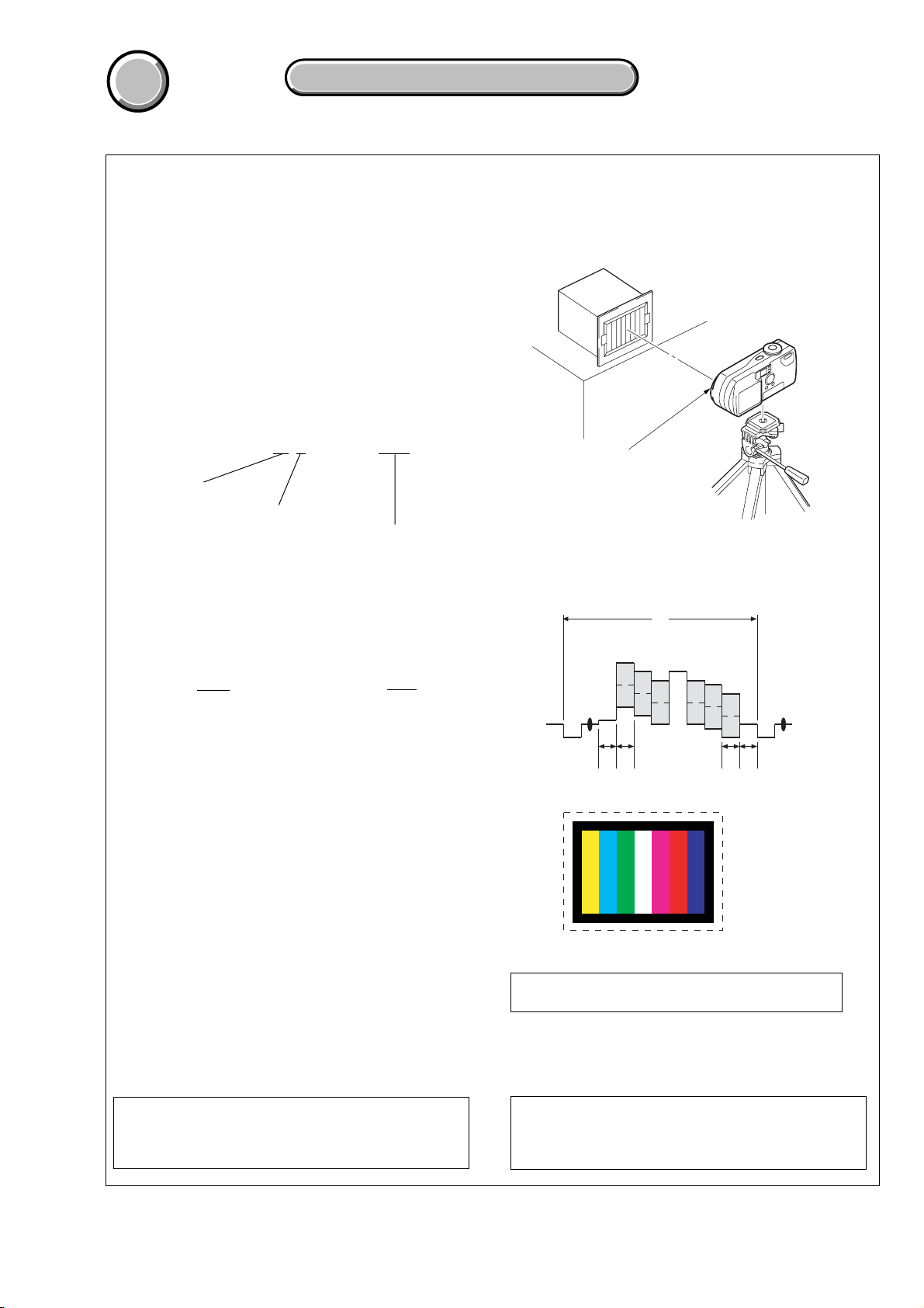
1. Connection
Pattern box
L
Front of the lens
L = About 30 cm
2. Adjust the distance so that the output waveform of
Fig. a and the Fig. b can be obtain.
H
Yellow
Cyan
White
Magenta
Green
AABBA=B
Fig. a (Video output terminal output waveform)
Fig.b (Picture on monitor TV)
When indicating parts by reference number, please
include the board name.
Red
Blue
Note : The components identified by mark 0 or
dotted line with mark 0 are critical for safety.
Replace only with part number specified.
Note : Les composants identifiés par une marque
0 sont critiques pour la sécurité.
Ne les remplacer que par une pièce portant
le numéro spécifie.
4-5
Page 25
COVER
COVER
Link
Link
DSC-P9
4-2. SCHEMATIC DIAGRAMS
CD-397 BOARD
CD-397 BOARD
SW-368 BOARD (1/2) (CONTROL SWITCH)
SW-368 BOARD (1/2) (CONTROL SWITCH)
SW-368 BOARD (2/2)
SW-368 BOARD (2/2)
(LCD DRIVE, TIMING GENERATOR)
(LCD DRIVE, TIMING GENERATOR)
COMMON NOTE FOR SCHEMATIC DIAGRAMS WAVEFORMS
COMMON NOTE FOR SCHEMATIC DIAGRAMS WAVEFORMS
(CCD IMAGER)
(CCD IMAGER)
ST-70 BOARD (FLASH DRIVE)
ST-70 BOARD (FLASH DRIVE)
CONTROL SWITCH BLOCK
CONTROL SWITCH BLOCK
Page 26
COVER
COVER
4-2. SCHEMATIC DIAGRAMS CD-397 PRINTED WIRING BOARD
4-2. SCHEMATIC DIAGRAMS CD-397 PRINTED WIRING BOARD
DSC-P9DSC-P9
4-2. SCHEMATIC DIAGRAMS
1
2
CD-397 BOARD
A
B
C
D
E
F
CCD IMAGER(CCD BLOCK)
XX MARK:NO MOUNT
LND125
LND124
LND123
LND122
LND121
LND120
LND119
LND118
LND117
LND116
LND115
LND114
LND113
LND112
LND111
LND110
LND109
LND108
LND107
LND106
LND105
LND104
LND103
LND102
LND101
SIGNAL PATH
REC
05
SY-77 (1/10)
CN001
( PAGE 4-9)
25
PRE_LAMP
24
23
22
21
20
19
18
17
16
15
14
13
12
11
CCD_TEMP
10
9
VSUB_CONT
8
7
CAM_-7.5V
6
5
4
3
2
1
Y/CHROMA
For Schematic Diagram
• Refer to page 4-41 for printed wiring board.
3
Note: voltage and waveform of mounted on CD-397 board
can not be measured, because they are (mounted)
by the side of the lens.
D101
TLOH20TP(SONY2)
SELF TIMER/
AF ILLUMINATOR
M_5V
CCD_GND
CCD_GND
CCD_GND
CCD_OUT
CCD_GND
CCD_GND
V4
V3A
V3B
V1B
V1A
VSHUT
CAM_15V
VIDEO
SIGNAL
V2
TH101
GND
GND
H1
RG
H2
GND
(CCD TEMP SENSOR)
R109
XX
4
Q101
2SC4250(T5LSONY1)
BUFFER
R101
C101
C102
0.1u
XX
R105
0
R103
0
68
R102
R104
0
FB101
3300
C104
10u
16V
C103
0.1u
C106
0.1u
16V
C105
10p
7
8
9
10
GND
TEST
TEST
VOUT
VDD12RG13H214H115GND16VSHT17CSUB18VL19H120H2
11
R107
16V
C107
0.1u
220k
C108
2200p
DTC144EHT2L
SWITCH
Q102
7
R108
2700
1V42
V3A3V3B
IC101
ICX406AQF-13
IC101
C109
0.1u
4V25
V1A6V1B
22
R106
865
CCD IMAGER
Precautions for Replacement of CCD Imager
• The CD-397 board mounted as a repair part is not equipped
with a CCD imager.
When replacing this board, remove the CCD imager from the
old one and mount it onto the new one.
• If the CCD imager has been replaced, carry out all the
adjustments for the camera section.
• As the CCD imager may be damaged by static electricity from
its structure, handle it carefully like for the MOS IC.
In addition, ensure that the receiver is not covered with dusts
nor exposed to strong light.
4-7 4-8
CD-397
Page 27
DSC-P9
COVER
COVER
4-2. SCHEMATIC DIAGRAMS SW-368 PRINTED WIRING BOARD
4-2. SCHEMATIC DIAGRAMS SW-368 PRINTED WIRING BOARD
For Schematic Diagram
• Refer to page 4-47 for printed wiring board.
1
3
5
9116842
107
SW-368 BOARD (1/2)
A
CONTROL SWITCH(KEY BLOCK)
XX MARK:NO MOUNT
NO MARK:REC/PB MODE
CL001
BL_VO-
CL002
BL_VO-
CL003
EVER_3.0V
CL004
KEY_AD0
KEY_AD1
PANEL_V
LCD_SO
KEY_AD3
XLCD_SCK
REG_GND
REG_GND
REG_GND
REG_GND
REG_GND
PANEL_R
PANEL_G
PANEL_B
REG_GND
PANEL_VG
XRST_SYS
A_4.9V
A_4.9V
CAM_15V
CAM_15V
HDO
CL005
CL006
CL007
CL008
CL009
CL010
CL011
CL012
CL013
CL014
CL015
CL016
CL017
CL018
CL019
CL020
CL021
CL022
CL023
CL024
CL025
CL026
CL027
CL028
CL029
CL030
CL031
CL032
CL033
B
AE_LOCK_LED
XCHARGE_LED
PANEL_HDO
XTALLY_LED
PANEL_2.9V
PANEL_2.9V
C
SY-77 (6/10)
CN701
(SEE PAGE 4-20)
XCS_PANEL_TG
D
PANEL_COM
E
F
SIGNAL PATH
VIDEO SIGNAL
CHROMA
REC
G
PB
H
I
BL_VO-
BL_VO-
PANEL_HDO
PANEL_V
LCD_SO
XCS_PANEL_TG
XLCD_SCK
PANEL_R
PANEL_G
PANEL_B
PANEL_COM
PANEL_VG
XRST_SYS
A_4.9V
A_4.9V
HDO
R012
1200
LEFT
13.4
R009
820
R008
330
R007
560
LND001
STATIC_GND
D004
TALLY(RED)
D003
AE_LOCK(GREEN)
STROBO/CHARGE_LED(YELLOW)
D002
(YELLOW)
W
W ZOOM T
R010
1200
R011
1500
B1
T
S002S001
PANEL_R
PANEL_G
PANEL_B
XRST_SYS
HDO
PANEL_V
LCD_SO
XLCD_SCK
XCS_PANEL_TG
A_4.9V
BL_VO-
PANEL_HDO
PANEL_VG
PANEL_COM
B2
R018
470
2.2
0
Q004
UN9213J-(K8).SO
LED DRIVE
D001
MAZT082H08S0
D006
C002
0.22u
MAZT082H08S0
R002
33k
0.5%
R003
240k
0.5%
13.3
D005
MAZT082H08S0
R005
100k
14.1
2
14
12.9
R006
100k
15.2
36
HN1C01FU-TE85R
D004
CL-196HR-CD-T
D003
CL-196YG-CD-T
D002
SML-310YTT86
MAZT082H08S0
Q003
HN1A01FU-TE85R
B+ SWITCH
14.5
2
1
4
14.1
5
13.4
5
Q002
B+ SWITCH
D007
R004
XX
6
3
S004
CONTROL
1200
RIGHT
SET
DOWN
B1
2
4
B2
DISPLAY
S005
R015
1500
R014
3300
A1
1
3
A2
(2/2)
1
UP
R013
A1
2
1
4
3
A2
S003
MENU
PANEL_13.5V
REG_GND
PANEL_2.9V
PANEL_R
PANEL_G
PANEL_B
XRST_SYS
HDO
PANEL_V
LCD_SO
XLCD_SCK
XCS_PANEL_TG
A_4.9V
BL_VO-
PANEL_HDO
PANEL_VG
PANEL_COM
SW-368 (1/2)
05
4-29 4-30
Page 28

COVER
COVER
For Schematic Diagram
• Refer to page 4-47 for printed wiring board.
• Refer to page 4-54 for waveforms.
4-2. SCHEMATIC DIAGRAMS SW-368 PRINTED WIRING BOARD
4-2. SCHEMATIC DIAGRAMS SW-368 PRINTED WIRING BOARD
DSC-P9DSC-P9
1
3
SW-368 BOARD (2/2)
A
LCD DRIVE,TIMING GENERATOR(RGB/TG BLOCK)
NO MARK:REC/PB MODE
B
C
PANEL_13.5V
PANEL_2.9V
D
PANEL_B
PANEL_G
E
F
1
PANEL_R
PANEL_V
LCD_SO
XLCD_SCK
XCS_PANEL_TG
HDO
(1/2)
REG_GND
G
H
A_4.9V
BL_VO-
XRST_SYS
PANEL_HDO
PANEL_VG
PANEL_COM
I
J
K
C101
L101
47u
47uH
6.3V
R135
150k
D102
MA8036-TX
R134
56k
1.5
Q108
2SB1462JQR(K8).SO
REF VOLTAGE GEN
68
0.5%
Q106
DRIVE
3.4
1510
R136
68
0.5%
4.0
2SB1462JQR(K8).SO
BACK LIGHT
0.9
C123
0.1u
Q109
DRIVE
TEST
24
COM
23
VST
22
VCK
21
EN
20
DWN
19
VDD
18
VSS
17
VDDG
16
VSSG
15
CS
14
WIDE
13
HST
12
REF
11
SDUT
10
9
CRext
HCK2
8
HCK1
7
PSIG
6
5
G
4
R
3
B
2
RGT
1
TEST2
CN101 6P
6
BL_THH
5
N.C.
4
BL_THL
3
BL_H
2
N.C.
BL_L
1
24PCN102
PANEL UNIT
LCD901
COLOR
LCD
MONITOR
D901
BACK LIGHT
5
C108
0.01u
1.2
37
XC.SAVE
XLCD_SCK
R106
470k
C103
0.01u
C102
0.1u
R104
33k
R105
33k
XTG_SO
XCS_PANEL_TG
C104
0.01u
XP.SAVE
C105
0.01u
C106
0.01u
C107
0.01u
2.9
38
2.9
39
2.2
40
2.9
41
2.9
42
1.2
43
1.2
44
2.9
45
1.8
46
1.8
47
1.8
48
N.C./C_BG
XC.SAVE
XSCK
SI
XCS
Vcc1
TRAP_ADJ
LPF_ADJ
XP.SAVE
B_IN
G_IN
R_IN
R107
15k
684 172
36
N.C./R_INJECT
5
6
35
EXT_DA
34
N.C
7
L102
10uH
C110
C111
0.1u
4.7u
20V
BLK
FRP
BGP
PRG
PFRP
13.41.77.12.91.51.42.902.80.50.7
26
27VP28
29
30
31
32
33
FRP
BGP
PRG
IC101
LCD DRIVER
IC101
RB5P004AM1
PFRP
BLACK_IN
25
XVP.SAVE
Vcc2
P_DC_DET
4
3
B_DC_DET
2
G_DC_DET
1
R_DC_DET
GND2/N.C.
GND1
VREF
Vcc3
COM_OUT
COM_IN
91411 12 16
R115
10
C116
2.2u
R116
7.1
24
VB
VG
VR
C117
2.2u
1.7
23
7.1
22
C118
2.2u
1.7
21
1.7
20
C119
2.2u
1.7
19
18
17
16
13.4
15
14
13
10
R117
10
R118
10
R119
R120
100k
100k
C120
4.7u
R122
100k
R121
100k
13
Q107
MCH3310-TL-E
SWITCH
13.4
13.4
S
XP_OFF
D
G
0
0
2.9
Q105
UN9213J-
(K8).SO
SWITCHING
VST
VCK
EN
DWN
C122
1u
WIDE
HST
HCK2
HCK1
R127
470k
7
PANEL_V
LCD_SO
XLCD_SCK
XCS_PANEL_TG
HDO
BGP
PRG
BLK
FRP
PFRP
XLCD_SCK
XCS_PANEL_TG
XTG_SO
LCD_SO
PANEL_V
L104
47uH
R139
1k
C126
2200p
C124
0.01u
XSH.SAVE2SH_R3SH_G4SH_B5SH_A6GND/N.C.7BIAS8OP_IN+9OP_IN-10OP_OUT11VCO12COM_DC
1
2.9 2.90.9 0.9 0.9 1.4 1.4 1.4 1.5 2.9 6.7
SH_R
SH_A
SH_B
SH_G
C109
1u
2.8
37
XCLP
2.9
38
PRG
0
39
SBLK
1.4
40
FRP
1.4
41
PFRP
2.9
42
XSCK
2.9
43
VDD
2.3
44
XCS
2.9
45
SO
2.9
46
SI
47
VDO
2.9
48
XVD
10
2700
R108
R109
47k
R111
22k
SH_R
SH_G
0.9
3.0
34
36
SHG35SHR
XCLR
68k
R110
C112
560p
SH_A
SH_B
0.90.9
31
32
VSS
SHA33SHB
IC102
LCD TIMING GENERATOR
IC102
CXD3512R-T4
RGT
R126
10k
0.1u
C113
R114
R113
100k
1M
R112
68k
2.92.9
29
30
RPD
TEST
D101
1SV290(TPL3)
C115
0.001u
L103
6.8uH
C114
82p
XP.SAVE
XC.SAVE
2.91.41.42.91.4
25
26
27
28
OSCI
OSCO
XC.SAVE
XSTBY
XP_OFF
TSTEN
0
24
VST
1.4
23
VCK
2.6
22
EN
2.9
21
DWN
0.2
20
WIDE
2.9
19
VDD
0
18
HST
1.4
17
HCK2
1.4
16
HCK1
2.9
15
RGT
2.9
14
13
9
VST
VCK
EN
DWN
WIDE
C125
0.01u
HST
HCK2
HCK1
RGT
XP_OFF
C121
1u
7.1
Q101
XP4601-TXE
PSIG DRIVE
R123
8200
Q102
7.7
XP4601-TXE
PSIG DRIVE
7.1
6.5
664
2
331
6.5
R124
10k
R125
2200
R137
10k
7.1
5
5
6.5
3.3
3.3
R138
47k
0.5%
13.4
4
1
7.1
IC103
TC75S55FU(TE85R)
VCC
123
IC103
BACK LIGHT
CONTROL
2
7.7
R131
470k
0.5%
R132
27k
0.5%
4.8
3.9
45
Q103
2SD2216J-
QR(K8).SO
BACK LIGHT
DRIVE
2.9
4.8
R129
3300
Q104
UN9213J-(K8).SO
BACK LIGHT
DRIVE
0.8
R133
R130
10k
0.5%
2SB1462J-
R128
QR(K8).SO
3300
BACK LIGHT
4.0
3.4
0.9
0.1
SIGNAL PATH
VIDEO SIGNAL
L
05
REC
CHROMA
HDO
PB
8
4-31
HD2HDO3XWRT4BL_ON5DETIN6GND7TST08LED9PWM10TEST11TEST12TEST
1
2.7 0.3 2.9 2.9
The components identified by mark 0 or dotted
line with mark 0 are critical for safety.
Replace only with part number specified.
4-32
Les composants identifiés par une marque 0 sont
critiques pour la sécurité. Ne les remplacer que
par une piéce portant le numéro spécifié.
SW-368 (2/2)
Page 29

COVER
COVER
For Schematic Diagram
• Refer to page 4-51 for printed wiring board.
4-2. SCHEMATIC DIAGRAMS ST-70 PRINTED WIRING BOARD
4-2. SCHEMATIC DIAGRAMS ST-70 PRINTED WIRING BOARD
DSC-P9DSC-P9
A
B
C
D
E
1
ST-70 BOARD
FLASH DRIVE(FL BLOCK)
NO MARK:REC/PB MODE
SY-77 (9/10)
CN351
(PAGE 4-26)
LND001
LND002
LND003
LND004
LND005
LND006
LND007
LND008
LND009
LND010
LND011
LND012
LND013
LND014
LND015
1
2
3
4
5
6
7
8
9
10
11
12
13
14
15
VL_3V
STB_ON1
STB_FULL
ST_UNREG
ST_UNREG
ST_UNREG
ST_UNREG
ST_UNREG
REG_GND
REG_GND
REG_GND
REG_GND
REG_GND
REG_GND
REG_GND
3 107
D001
MA2S111-(K8).SO
C002
1u
BT001
LITHIUM
BATTERY
(BACK UP)
0
0
R002
27k
0
Q001
2SB1073-R-TX
TRANS DRIVE
R001
47
C001
0.01u
R004
270
R003
2700
5
D002
HAU160C030TP
T001
4
F
3
2
P
1
5
S
6
C003
135uF
CHARGING
CAPACITOR
R005
47
187.6
R006
1M
Q002
CY25AAJ-8-T13
FLASH DRIVE
0
R007
1M
1/10W
C004
0.047u
L001
96842
LND016
XE_A
LND017
TRIGGER
LND018
XE_K
FLASH
UNIT
05
The components identified by mark 0 or dotted
line with mark 0 are critical for safety.
Replace only with part number specified.
4-35
Les composants identifiés par une marque 0 sont
critiques pour la sécurité. Ne les remplacer que
par une piéce portant le numéro spécifié.
4-36
ST-70
Page 30

DSC-P9
COVER
COVER
DSC-P9
COVER
COVER
4-2. SCHEMATIC DIAGRAMS
4-2. SCHEMATIC DIAGRAMS
For Schematic Diagram
1
CONTROL SWITCH BLOCK
A
CONTROL SWITCH BLOCK is replaced as a block,
so that PRINTED WIRING BOARD is omitted.
2
B
(1st)
C
D
S003
(SHUTTER)
(2nd)
R001
20k
123456789
14P
XAE_LOCK_SW
D_2.9V
XSHTR_SW
NC
MODE_DIAL
GND
NC
XPB_ON
1011121314
XMOVIE
XSET_UP
XPWR_LED
3
SET_UP
B
G
MOVIE
6
PLAY
A
(5 POSITION MODE_DIAL)
D001
(POWER(GREEN))
NC
XPWR_ON
PWR_LED_VCC
S005
MODE DIAL
45
R003
R002
4000
6000
S004
POWER
SCN
2
P_AUTO
1
E
05
SY-77 (7/10)
CN704
(SEE PAGE 4-21)
CONTROL SWITCH BLOCK
4-38
Page 31

4-3. PRINTED WIRING BOARDS
COVER
COVER
4-3. PRINTED WIRING BOARDS
4-3. PRINTED WIRING BOARDS
THIS NOTE IS COMMON FOR WIRING BOARDS
(In addition to this, the necessary note is printed in each block)
(For printed wiring boards)
• : Uses unleaded solder.
• : Circuit board
: Flexible board
Pattern from the side which enables seeing.
(The other layers’ patterns are not indicated)
• Through hole is omitted.
• Circled numbers refer to waveforms.
• There are a few cases that the part printed on diagram
isn’t mounted in this model.
• C: panel designation
• Chip parts.
Transistor Diode
C
DSC-P9
43
12
3
43
12
31
4625
4
3
12
5
5246
EB
654
123
31
21
12
345
534
54
45
21321321
123
312
43
12
21
34
4-39
Page 32

COVER
COVER
Link
Link
DSC-P9
4-3. PRINTED WIRING BOARDS
CD-397 BOARD
CD-397 BOARD
SW-368 BOARD
SW-368 BOARD
MOUNTED PARTS LOCATION
MOUNTED PARTS LOCATION
ST-70 BOARD
ST-70 BOARD
CIRCUIT BOARDS LOCATION
CIRCUIT BOARDS LOCATION
WAVEFORMSCOMMON NOTE FOR PRINTED WIRING BOARDS
WAVEFORMSCOMMON NOTE FOR PRINTED WIRING BOARDS
Page 33

DSC-P9DSC-P9
SELF TIMER/
AF ILLUMINATOR
COVER
COVER
CD-397 (CCD IMAGER)
• For Printed Wiring Board.
• :Uses unleaded solder.
• There are a few cases that the part isn't mounted in this
model is printed on this diagram.
4-2. SCHEMATIC DIAGRAMS 4-3. PRINTED WIRING BOARDS
4-2. SCHEMATIC DIAGRAMS 4-3. PRINTED WIRING BOARDS
MOUNTED PARTS LOCATION
MOUNTED PARTS LOCATION
4-41 4-42
CD-397
Page 34

DSC-P9
4-2. SCHEMATIC DIAGRAMS 4-3. PRINTED WIRING BOARDS
COVER
COVER
4-2. SCHEMATIC DIAGRAMS 4-3. PRINTED WIRING BOARDS
SW-368 (FRONT CONTROL, LCD DRIVE, TIMING GENERATOR, CONTROL SWITCH)
• For Printed Wiring Board.
• :Uses unleaded solder.
• There are a few cases that the part isn't mounted in this
model is printed on this diagram.
• See page 4-57 for printed parts location.
D004
(TALLY (RED))
D003
(AE LOCK (GREEN))
D002
(STROBO/CHARGE LED)
A
KK
KK
A
A
KK
6
7
1
3
5
4
2
ZOOMW T
K
A
K
MOUNTED PARTS LOCATION
MOUNTED PARTS LOCATION
CONTROL
DISPLAY MENU
10
8
9
SW-368
4-47 4-48
Page 35

DSC-P9
COVER
COVER
ST-70 (FLASH DRIVE)
• For Printed Wiring Board.
• :Uses unleaded solder.
• There are a few cases that the part isn't mounted in this
model is printed on this diagram.
FLASH UNIT
4-2. SCHEMATIC DIAGRAMS 4-3. PRINTED WIRING BOARDS
4-2. SCHEMATIC DIAGRAMS 4-3. PRINTED WIRING BOARDS
MOUNTED PARTS LOCATION
MOUNTED PARTS LOCATION
C
BE
6
3
5
A
K
A
1
2
4
BT001
BATTERY,
LITHIUM SECONDARY
11, 12
11, 12
ST-70
4-51 4-52
Page 36

DSC-P9
SW-368 BOARD
COVER
COVER
SW-368 BOARD
SW-368 BOARD
1
2
3
2H
IC101 w; REC/PB
2H
IC101 ws REC/PB
7.8 Vp-p
7.8 Vp-p
6
340 mVp-p
H
IC101 rj REC/PB
7
460 mVp-p
H
IC101 rk REC/PB
8
4
5
2H
2H
IC101 wf REC/PB
2H
IC101 wj REC/PB
7.8 Vp-p
5.1 Vp-p
340 mVp-p
3.0 Vp-p
H
IC102 1 REC/PB
9
4.1 Vp-p
11.28 MHz
IC102 wj REC/PB
q;
3.0 Vp-p
SW-368
H
IC101 rh REC/PB
V
IC102 rk REC/PB
4-54
Page 37

COVER
COVER
SW-368 BOARD
C002 C-2
C101 B-2
C102 B-3
C103 B-4
C104 B-4
C105 B-4
C106 B-3
C107 B-3
C108 B-4
C109 B-2
C110 B-2
C111 C-3
C112 C-3
C113 C-3
C114 B-3
C115 B-3
C116 C-4
C117 C-4
C118 C-4
C119 C-4
C120 C-3
C121 C-3
C122 B-2
C123 A-2
C124 A-3
C125 A-2
C126 B-3
CN101 C-1
CN102 B-1
D001 A-1
D002 A-1
D003 A-1
D004 A-1
D005 A-2
D006 A-2
D007 A-4
D101 B-3
D102
IC101 B-4
IC102 A-3
IC103 C-3
L101 B-2
L102 C-3
L103 B-3
L104 B-2
Q002 C-2
Q003 C-2
Q004 A-2
Q101 B-4
Q102 B-4
Q103 C-2
Q104 C-3
Q105 A-2
Q106 C-2
Q107 A-2
Q108 A-3
Q109 C-2
R002 C-2
R003 C-2
R005 B-2
R006 C-2
R007 A-2
R008 A-2
R009 A-2
R010 A-4
R011 C-2
R012 B-1
R013 B-1
R014 C-1
R015 C-1
R018 A-2
R104 B-4
R105 B-4
R106 B-3
R107 B-4
R108 B-3
R109 B-3
R110 B-3
R111 B-3
R112 C-3
R113 C-3
R114 B-3
R115 C-4
R116 C-4
R117 C-4
R118 C-4
R119 C-4
R120 C-4
R121 C-3
R122 C-4
R123 B-4
R124 B-4
R125 C-3
R126 A-3
R127 A-2
R128 C-1
R129 C-3
R130 C-3
R131 A-3
R132 A-3
R133 C-2
R134 A-3
R135 A-2
R136 C-1
R137 B-4
R138 C-3
R139 C-3
S001 A-3
S002 A-4
S003 C-2
S004 B-1
S005 C-1
4-3. PRINTED WIRING BOARDS
4-3. PRINTED WIRING BOARDS
DSC-P9
4-57
4-57E
SW-368
Page 38

COVER
COVER
Before starting adjustment
EVR Data Re-writing Procedure When Replacing Board
The data that is stored in the repair board, is not necessarily correct.
Perform either procedure 1 or procedure 2 or procedure 3 when replacing board.
Procedure 1
Save the EVR data of the machine in which a board is going to be replaced. Download the saved data after a
board is replaced.
DSC-P9
SECTION 5
ADJUSTMENTS
(Machine before starting repair)
Save the EVR data
to a personal computer.
Procedure 2
Remove the EEPROM from the board of the machine tha t is going to be repaired. Install the removed EEPR OM
to the replaced board.
PC
Remove the EEPROM and install it.
(Former board)
(New board)
PC
Download the saved
data to a machine.
(Machine after a board is replaced)
Procedure 3
When the data cannot be saved due to defective EEPROM, or when the EEPROM cannot be removed or installed, save the data from the same model of the same destination, and download it.
(Machine to be repaired)
Download the data.
Save the data.
(The same model of the same destination)
After the EVR data is saved and downloaded, check the
respective items of the EVR data.
(Refer to page 5-2 for the items to be checked.)
(Machine to be repaired)PC
5-1
Page 39

DSC-P9
1-1. Adjusting items when replacing main parts and boards
When replacing main parts and boards, adjust the items indicated by z in the following table.
Block
replacement
Replaced parts
Mounted parts
replacement
Board
replacement
Adjustment section Adjustment
Initialization of A, B, D,
E, F, 7, 9 page data
Video Video sync level adj.
Camera Flange back adj.
LCD LCD initial data input
Initialization of A, D page data
Initialization of B, E, F, 7, 9, page data
Video burst level check
F No. compensation
Mechanical shutter adj.
Light value adj.
Mixed color cancel adj.
Auto white balance standard data input
CCD linearity check
Color reproduction adj.
CCD (white and black) defect
compensation
Strobe white balance adj.
VCO adj.
Black limit adj.
Bright adj.
Contrast adj.
VG Center adj.
PSIG Gray adj.
V-COM adj.
White balance adj.
(LCD panel)
(Back light unit)
(CCD imager)
(Camera Module)
(EVR)
(CAMERA DSP)
(VIDEO AMP)
(LCD drive)
LCD901
D901
IC101
IC508
IC601
IC101
(LCD Timing generator)
IC101
IC102
(COMPLETE)
EEPROM
(COMPLETE) (Note)
(COMPLETE)
IC505
RadarWRadarWRadarWRadarWRadarWRadarW
Lens block assy (Note)
Flash unit
LCD block
LCD block
CD-397 board
CH-111 board
SY-77 board
SY-77 board
SY-77 board
SW-368 board
SW-368 board
ST-70 board
SY-77 board
SW-368 board
SY-77 board
Supporting
zz
zz
zzz z z
zzz
zz zzz
zz zzz
zz zzz
zzz zzz
zzz zzz
zzz zzz
zz
zzz zzz
zzzzz
z zzz zz zz
zzz
z zzz
z zzz
z zzz
z zzz
z zzz
z zzz
z z zzz
zz z zzz
Table 5-1-1
Note : When replacing the lens block or the SY-77 board, refer to “Precaution on Replacing the Lens Block or the SY-77 board”. (See
page 6)
5-2
Page 40

Ref. No.
J-1
J-2
J-3
J-4
J-5
J-6
J-7
J-8
Name
Filter for color temperature correction (C14)
Pattern box PTB-450
Color bar chart for pattern box
Adjusting remote commander (RM-95 upgraded).
(Note 1)
Siemens star chart
Clear chart for pattern box
CPC-9 jig (Note 2)
Minipattern box
Parts Code
J-6080-058-A
J-6082-200-A
J-6020-250-A
J-6082-053-B
J-6080-875-A
J-6080-621-A
J-6082-393-C
J-6082-353-B
Usage
Auto white balance adjustment/check
White balance adjustment/check
For checking the flange back
For connecting the adjusting remote commander
For adjusting the LCD block
For adjusting the flange back
J-9 Back ground paper J-2501-130-A For adjusting the strobe
5-1. CAMERA SE CTION ADJUSTMENT
1-1. PREPARATIONS BEFORE ADJUSTMENT
1-1-1. List of Service Tools
• Oscilloscope • Color monitor • Vectorscope
• Regulated power supply • Digital voltmeter
DSC-P9
Note 1: If the micro processor IC in the adjusting remote
commander is not the new micro processor (UPD7503GC56-12), The pages cannot be switched. In this case,
replace with the new micro processor (8-759-148-35).
J-1 J-5J-2
J-6 J-7
J-3 J-4
J-8 J-9
Note 2: The old CPC-9 jig (Parts code: J-6082-393-B) cannot be
used, because it cannot operate the adjusting remote commander.
Fig. 5-1-1
5-3
Page 41

DSC-P9
1-1-2. Preparations
Note 1: For details of how remove the cabinet and boards, refer
to “2. DISASSEMBLY”.
Note 2: When performing only the adjustments, the lens block
and boards need not be disassemble.
1) Connect the equipment for adjustments according to Fig. 5-1-
6.
2) Connect the Adjusting remote commander to SY-77 board
CN706 via CPC-9 jig (J-6082-393-C). (See Fig. 5-1-3)
Note 3: Setting the “Forced CAMERA mode power ON” Mode
1) Select page: 0, address: 01, and set data: 01.
2) Select page: D, address: 21, set data: 03, and press
the PAUSE button of the adjusting remote commander.
The above procedure will enable the camera power
to be turned on. After completing adjustments, be
sure to exit the “Forced CAMERA mode power ON
Mode”.
Note 4: Exiting the “Forced CAMERA mode power ON Mode”
1) Select page: 0, address: 01, and set data: 01.
2) Select page: D, address: 21, set data: 00, and press
the PAUSE button of the adjusting remote commander.
3) Select page: 0, address: 01, and set data: 00.
Pattern box
L
Front of the lens
L = About 30 cm
Fig. 5-1-2
1-1-3. Discharging of the Flashlight Power Supply
The capacitor which is used as power supply of flashlight is charged
with 200 V to 300 V voltage. Discharge this voltage before starting adjustments in order to protect service engineers from electric
shock during adjustment.
Discharge procedure
1. Press the FLASH button (SW-368 board S004 (CONTROL
UP)) and set the NO FLASH mode.
2. Fabricate the discharging jig as sho wn in Fig. 5-1-5 locally by
yourself. Connect the discharging jig to the positive (+) and
negative (–) terminal of the flash voltag e charge capacitor . Allow ten seconds to discharge the voltage.
R:1 kΩ/1 W
(Part code:
1-215-869-11)
Capacitor
CPC-9 jig
(J-6082-393-C)
(Note 1, 2)
18
CPC cover
Note 1: Don’t use the 12 pin flexible board of CPC-9 jig.
It causes damage to the unit.
Note 2: The old CPC-9 jig (Parts code: J-6082-393-B)
cannot be used, because it cannot operate
the adjusting remote commander.
1
SY-77 board
CN706
Fig. 5-1-4
Fig. 5-1-3
1 kΩ/1 W
Wrap insulating tape.
Fig. 5-1-5
5-4
Page 42

ST-70 BOARD
JK-227 BOARD
SPEAKER
A/V OUT jack
J002
CN002
USB
jack
JK-226 BOARD
J001
DC IN jack
CONTROL SWITCH BLOCK
CN704
CN351
SY-77 BOARD
CN701
CN706
To battery terminal
Need not
connected
CN703
CN705
CN001
CN301
CN702
Must be connected
when the MIC UNIT
is used.
MIC
MS SOCKET
DSC-P9
AF
Illumination
LENS UNIT
Must be connected
when the Memory Stick
is used.
Terminated
75 Ω
Adjusting
remote
commander
Vectorscope
Color monitor
AC IN
AC power adaptor
CPC-9 jig (Note 1, 2)
(J-6082-393-C)
Audio
(Black)
Video (yellow)
18
1
CN101
CN102
SW-368 BOARD
PANEL UNIT
Regulated
power supply
(6.0 to 7.2 Vdc)
Note 1: Don’t use the 12 pin flexible board of CPC-9 jig.
It causes damage to the unit.
Note 2: The old CPC-9 jig (Parts code: J-6082-393-B)
cannot be used, because it cannot operate
the adjusting remote commander.
Fig. 5-1-6
5-5
Page 43

DSC-P9
1-1-4. Precautions
1. Setting the Switch
Unless otherwise specified, set the switches as follows and perform adjustments.
1. Mode Dial .......................................... CAMERA
2. ZOOM switch
(SW-368 board S001, S002).............. WIDE end
3. EV (Menu display) ............................ 0EV
4. DSIPLAY/LCD ON/OFF button
(SW-368 board S005) ........................ OSD OFF
5. WB (WHITE BALANCE)
(Menu display) ................................... AUTO
6. P.EFFECT (Menu display) ................ OFF
7. VIDEO OUT (SET UP setting)......... NTSC
2. Order of Adjustments
Basically carry out adjustments in the order given.
Color bar chart (Color reproduction adjustment frame)
H
Yellow
Cyan
White
Magenta
Green
AB B
A=B
Red
Blue
A
Enlargement
B
A
3. Subjects
1) Color bar chart (Standard picture frame).
When performing adjustments using the color bar chart, adjust the picture frame as shown in Fig. 5-1-7. (Standard picture frame)
2) Clear chart (Standard picture frame)
Remove the color bar chart from the pattern box and insert a
clear chart in its place. (Do not perform zoom operations during this time)
3) Chart for flange back adjustment
Join together a piece of white A0 size paper (1189mm × 841
mm) and a piece of black paper to make the chart shown in
Fig. 5-1-8.
C=D
V
Difference in level
DC
Fig. 5-1-7
Electronic beam scanning frame
Red
Cyan
White
Green
Yellow
Fig. b (monitor TV picture)
Adjust the camera zoom and direction to
obtain the output waveform shown in Fig a
and the monitor TV display shown in Fig. b.
Black
Magenta
1189 mm
Blue
CRT picture frame
White
841 mm
Note: Use a non-reflecting and non-glazing vellum paper. The
size must be A0 or larger and the joint between the white
and black paper must not have any undulations.
Fig. 5-1-8
5-6
Page 44

4. Preparing the Flash Adjustment Box
A dark room is required to provide an accurate flash adjustment.
If it is not available, prepare the flash adjustment box as given
below;
1) Provide woody board A, B and C of 15 mm thickness.
DSC-P9
woody board A (2)
530 mm
(400 mm)
1026 mm: Depth 1 m
(513 mm: Depth 50cm)
1030 mm
(730 mm)
woody board B (2)
500 mm
(370 mm)
1000 mm
(700 mm)
Fig. 5-1-9
2) Apply black mat paint to one side of woody board A and B.
3) Attach background paper (J-2501-130-A) to woody board C.
4) Assemble so that the black sides and the background paper
side of woody board A, B and C are internal. (Fig 5-1-10)
1026 mm: Depth 1 m
(513 mm: Depth 50cm)
woody board A
woody board B
woody board C (1)
1000 mm
(700 mm)
1000 mm
(700 mm)
woody board B
woody board C
Fig. 5-1-10
woody board A
5-7
Page 45

DSC-P9
1-2. INITIALIZATION OF A, B, D, E, F, 7, 9 PAGE
DAT A
1-2-1. Initialization of A, D Page Data
1. Initializing A, D Page Data
Note: If the A, D page data has been initialized, the following
adjustments need to be performed again.
1) Modification of A, D page data
2) Video system adjustments
3) LCD system adjustments
4) System control system adjustments
Adjsuting page A
Adjsuting Address 00 to FF
Adjusting page D
Adjusting Address 10 to 73
Initializing Method:
Order Page Address Data Procedure
1 0 01 01
24 030B
34 002D
4 4 01 2D Press PAUSE button.
5 4 02 Check the data changes to “01”.
6
2. Modification of A, D Page Data
If the A, D page data has been initialized, change the data of the
“Fixed data-2” address shown in the following table by manual
input.
Perform “Modification of
A, D page Data”.
3. A Page table
Note 1: Fixed data-1: Initialized data.
(Refer to “1. Initializing the A Page Data”)
Note 2: Fixed data-2: Modified data.
(Refer to “2. Modification of A Page Data”)
Address Initial value Remark
00, 01 Fixed data-1 (Initialized data)
02 00 Test mode
03 to 81 Fixed data-1 (Initialized data)
82 6A VCO adj. (NTSC)
83 7C VCO adj. (PAL)
84 20 V-COM adj.
85 BC Bright adj.
86 08 Black limit adj.
87 BF Psig Gray adj.
88 94
89 7A
8A 3F Contrast adj.
8B 3F VG Center adj.
8C Fixed data-1 (Initialized data)
8D Fixed data-2
8F to 9F Fixed data-1 (Initialized data)
A0 80 Video sync level adj.
A1 to A8 Fixed data-1 (Initialized data)
A9 Fixed data-2
AA to FF Fixed data-1 (Initialized data)
White balance adj.
Modifying Method:
1) Before changing the data, select page: 0, address: 01, and set
data: 01.
2) New data for changing are not shown in the tables because
they are different in destination. When changing the data, copy
the data built in the same model.
Note: If copy the data built in the different model, the
camera may not operate.
3) W hen changing the data, press the PAUSE button of the
adjusting remote commander each time when setting new data
to write the data in the non-volatile memory.
4) Check that the data of adjustment addresses is the initial value.
If not, change the data to the initial value.
Processing after Completing Modification of A, D Page Data:
Order Page Address Data Procedure
1 2 00 29
2 2 01 29 Press PAUSE button.
4. D Page table
Note 1: Fixed data-1: Initialized data.
(Refer to “1. Initializing the D Page Data”)
Note 2: Fixed data-2: Modified data.
(Refer to “2. Modification of D Page Data”)
Address Initial value Remark
10 to 20 Fixed data-1 (Initialized data)
21 00 Test mode
22 to54 Fixed data-1 (Initialized data)
55 Fixed data-2
56 to 73 Fixed data-1 (Initialized data)
5-8
Page 46

DSC-P9
1-2-2. Initialization of B, E, F, 7, 9 Page Data
1. Initializing B, E, F, 7, 9 Page Data
Note: If the B, E, F, 7, 9 Page data has been initialized,
“Modification of B, E, F, 7, 9 Page Data” and following
adjustments need to be performed again.
1) Modification of B, E, F, 7, 9 page data
2) Camera system adjustments
Adjusting page B
Adjusting Address 00 to FF
Adjusting page E
Adjusting Address 00 to FF
Adjusting page F
Adjusting Address 00 to FF
Adjusting page 7
Adjusting Address 00 to FF
Adjusting page 9
Adjusting Address 00 to FF
Initializing Method:
Order Page Address Data Procedure
1 0 01 01
26 030B
36 002D
4 6 01 2D Press PAUSE button.
5 6 02 Check the data changes to “01”.
6
Perform “Modification of B,
E, F, 7, 9 page Data”.
3. B Page Table
Note 1: Fixed data-1: Initialized data.
(Refer to “1. Initializing B, E, F, 7, 9 Page Data”)
Note 2: Fixed data-2: Modified data.
(Refer to “2. Modification of B, E, F, 7, 9 Page Data”)
Address Initial value Remark
00 to 6D Fixed data-1 (Initialized data)
6E Fixed data-2
6F to FF Fixed data-1 (Initialized data)
4. E Page Table
Note 1: Fixed data-1: Initialized data.
(Refer to “1. Initializing B, E, F, 7, 9 Page Data”)
Note 2: Fixed data-2: Modified data.
(Refer to “2. Modification of B, E, F, 7, 9 Page Data”)
Address Initial value Remark
00 to 94 Fixed data-1 (Initialized data)
95 Fixed data-2
96 Fixed data-2
97 to CF Fixed data-1 (Initialized data)
D0 Fixed data-2
D1 to FF Fixed data-1 (Initialized data)
2. Modification of B, E, F, 7, 9 Page Data
If the B, E, F, 7, 9 Page data has been initialized, change the data
of the “Fixed data-2” address shown in the following tables by
manual input.
Modifying Method:
1) Before changing the data, select page: 0, address: 01, and set
data: 01.
2) New data for changing are not shown in the tables because
they are different in destination. When changing the data, copy
the data built in the same model.
Note: If copy the data built in the different model, the
camera may not operate.
3) When changing the data, press the PAUSE button of the
adjusting remote commander each time when setting new data
to write the data in the non-volatile memory.
4) Check that the data of adjustment addresses is the initial value.
If not, change the data to the initial value.
Processing after Completing Modification of B, E, F, 7, 9
Page data
Order Page Address Data Procedure
1 2 00 29
2 2 01 29 Press PAUSE button.
5-9
Page 47

DSC-P9
5. F Page Table
Note 1: Fixed data-1: Initialized data.
(Refer to “1. Initializing the B, E, F, 7, 9 Page Data”)
Note 2: Fixed data-2: Modified data.
(Refer to “2. Modification of B, E, F, 7, 9 Page Data”)
Address Initial value Remark
00 to 0F Fixed data-1 (Initialized data)
10 FF
11 FF
12 FF
13 FF
14 FF
15 FF
16, 17 Fixed data-1 (Initialized data)
18 36
19 54
1A 87
1B 71
1C 10
1D C0
1E 00
1F 00
20 00
21 00
22 00
23 00
24 20
25 20
26 13
27 46
28 0A
29 00
2A 00
2B 00
2C 00
2D 00
2E 00
2F 00
30 00
31 00
32 00
33 00
34 00
35 00
36 00
37 00
38 00
39 00
3A 00
3B 00
3C 00
3D 00
AF Ilumination check.
Flange back adj.
Address Initial value Remark
3E FF Flange back adj.
3F Fixed data-1 (Initialized data)
40 00
41 00
42 00
43 00
44 00
45 00
46 00
47 00
48 00
49 00
4A 00
4B 00
4C 00
4D 00
4E 00
4F 00
50 00
51 00
52 00
53 00
54 to 5D Fixed data-1 (Initialized data)
5E 00
5F 00
60 00
61 00
62 00
63 00
64 00
65 30
67 6D
68 to 6D Fixed data-1 (Initialized data)
6E 00
6F 00
70 32
71 B2
72 23
73 64
74 32
75 6C
76 23
77 88
78 33
79 36
Flange back adj.
F No. compensation
Light value adj.66 FE
Mixed color cancel adj.
AWB 3200K standard data input 1
AWB 3200K standard data input 2
5-10
Page 48

DSC-P9
Address Initial value Remark
7A 22
7B 2C
7C 32
7D 68
7E 23
7F DF
80 33
81 93
82 22
83 7F
84 32
85 E2
86 25
87 12
88 20
89 F5
8A 33
8B 14
8C 20
8D E2
8E 33
8F 89
90 21
91 69
92 32
93 62
94 21
95 52
96 33
97 94
98 21
99 52
9A 30
9B 80
9C 23
9D A8
9E 33
9F C3
A0 2A
A1 48
A2 61
A3 B0
A4 03
A5 E9
A6 63
A7 83
A8 D5
A9 FE
AA 73
AWB 3200K standard data input 2
AWB 3200K standard data input 3
AWB 5800K standard data input 1
AWB 5800K standard data input 2
AWB 5800K standard data input 3
A WB 5800K standard data input 1, 2, 3
Color reproduction adj.
Address Initial value Remark
AB 45
AC 63
AD 83
AE 03
AF E9
B0 00 AWB 3200K standard data input 1
B1 00 AWB 5800K standard data input 1
B2 00 AWB 3200K standard data input 1
B3 00 AWB 5800K standard data input 1
B4 00 AWB 3200K standard data input 1
B5 Fixed data-1 (Initialized data)
B6 28
B7 6E
B8 10
B9 6B
BA 0F
BB F6
BC 0F
BD F7
BE 00
BF 00
C0 00
C1 00
C2 00
C3 00
C4 00
C5 00
C6 00
C7 30
C8 1B
C9 12
CA 00
CB 00
CC 80
CD 90
CE 98
CF 90
D0 88
D1 00
D2 00
D3 00
D4 00
D5 00
D6 00
D7 14
D8 to DA Fixed data-1 (Initialized data)
DB 00
DD 00
Color reproduction adj.
Strobe white balance adj.
Mechanical shutter adj.
Strobe white balance adj.DC 00
5-11
Page 49

DSC-P9
Address Initial value Remark
DE 00
DF 00
E0 00
E1 00
E2 00
E3 00
E4 00
E5 00
E6 00
E7 00
E8 00
E9 00
EA 00
EB 00
EC 00
ED 00
EE 00
EF 00
F0 to FF Fixed data-1 (Initialized data)
Strobe white balance adj.
6. 7 Page Table
Note 1: Fixed data-1: Initialized data.
(Refer to “1. Initializing B, E, F, 7, 9 Page Data”)
Note 2: Fixed data-2: Modified data.
(Refer to “2. Modification of B, E, F, 7, 9 Page Data”)
Address Initial value Remark
00 to FF Fixed data-1 (Initialized data)
7. 9 Page Table
Note 1: Fixed data-1: Initialized data.
(Refer to “1. Initializing B, E, F, 7, 9 Page Data”)
Note 2: Fixed data-2: Modified data.
(Refer to “2. Modification of B, E, F, 7, 9 Page Data”)
Address Initial value Remark
00 to FF Fixed data-1 (Initialized data)
5-12
Page 50

DSC-P9
1-3. VIDEO SYSTEM ADJUSTMENTS
1. Video Sync Level Adjustment
Adjust the sync level of the composite video signal output.
Mode PLAY
Signal Arbitrary
Measurement Point Video terminal of A/V OUT jack
(75 Ω terminated)
Measuring Instrument Oscilloscope
Adjustment Page A
Adjustment Address A0
Specified Value A = 286 ± 5 mVp-p (NTSC)
A = 300 ± 5 mVp-p (PAL)
Adjusting method:
Order Page Address Data Procedure
1 0 01 01
2 A 02 03 Press PAUSE button
34 F104
Change the data and set the
4A A0
5 A A0 Press PAUSE button
Processing after Completing Adjustments:
Order Page Address Data Procedure
1 A 02 00 Press PAUSE button
24 F100
3 0 01 00
sync level (A) to the specified
value.
2. Video Burst Level Check
Adjust the burst level of the composite video signal output.
Mode PLAY
Signal Arbitrary
Measurement Point Video terminal of A/V OUT jack
(75 Ω terminated)
Measuring Instrument Oscilloscope
Specified Value A = 286 ± 30 mVp-p (NTSC)
A = 300 ± 30 mVp-p (PAL)
Adjusting method:
Order Page Address Data Procedure
1 0 01 01
2 A 02 03 Press PAUSE button
34 F104
4A A0
5 A A0 Press PAUSE button
Processing after Completing Adjustments:
Order Page Address Data Procedure
1 A 02 00 Press PAUSE button
24 F100
3 0 01 00
Check that the burst level (A)
is satisfied the specified value.
H
Fig. 5-1-11
A
A
H
Fig. 5-1-12
5-13
Page 51

DSC-P9
1-4. CAMERA SYSTEM ADJUSTMENTS
Before perform the camera system adjustments, check that the
specified values of “VIDEO SYSTEM ADJUSTMENTS” are satisfied.
Note: For “CAMERA SYSTEM ADJUSTMENTS”, perform in
order of item numbers.
Data setting during camera system adjustments
Perform the following data setting before the camera system adjustments.
It is not necessary to perform the following data setting ev erytime
when you perform some items of camera system adjustments continuously unless the power is turned off. Only when the power is
turned off during this adjustments, perform the data setting again,
then continue the adjustments.
Set up setting:
1) VIDEO OUT of SET UP setting............... NTSC (NTSC mode)
(This adjustment must be performed in NTSC mode, so don't
set the SET UP setting to “PAL”)
Data setting method:
Order Page Address Data Procedure
1 0 01 01
Set the bit value of bit 5 is
2A 01
32 10
4A 00
5A 02
6 D 21 03 Press PAUSE button.
76 C1
86 6C01
9 Wait for 1 second.
10 B 6E 80 Press PAUSE button.
11 E 95 E0 Press PAUSE button.
12 E 96 00 Press PAUSE button.
13 E D0 10 Press PAUSE button.
Note 1: For the bit values, refer to “5-2. SERVICE MODE”,
“2-3. 2. Bit value discrimination”.
Note 2: In case of wrong data.
• Select page: 2, address: 00 and set data: 29.
• Select page: 2, address: 01 and set data: 29.
• Select page: 2, address: 0C, set the bit value of bit 1 is
1.
• Select page: 2, address: 04 and set data: 04.
Set the adjusting remote commander to normal LANC,
and the power will be turned, off and on automatically .
Note 3: Repeat the “Data setting method”, if the power was turned
off and on during the “CAMERA SYSTEM ADJUSTMENTS”.
“1”, and press PAUSE
button. (Note 1)
Check the bit values of bit3,
bit4 and bit5 are “1”.
(Note 1, 2)
Set the bit value of bit 1 is
“1”, and press PAUSE
button. (Note 1)
Set the bit value of bit 1 is
“1”, and press PAUSE
button. (Note 1)
Check the data changes to
“02”.
After completing the camera system adjustments,
release the data setting:
Order Page Address Data Procedure
1 E 96 40 Press PAUSE button.
2 B 6E B0 Press PAUSE button.
36 6C00
4 D 21 00 Press PAUSE button.
Set the bit value of bit 1 is
5A 02
6A 00
7A 01
8 0 01 00
“0”, and press PAUSE
button. (Note 1)
Set the bit value of bit 1 is
“0”, and press PAUSE
button. (Note 1)
Set the bit value of bit 5 is
“0”, and press PAUSE
button. (Note 1)
5-14
Page 52

DSC-P9
Color bar chart picture frame
Monitor TV picture frame
E=F
V
EF
Picture Frame Setting
Mode CAMERA
Subject Color bar chart
(Standard picture frame with the
zoom lens at WIDE end)
Measurement Point Video terminal of A/V OUT jack
(75 Ω terminated)
Measuring Instrument Oscilloscope and monitor TV
Specified Value A=B, C=D, E=F
Note 1: Displayed data of the page 1 of adjusting remote com-
mander.
1:
XX:XX
YL data
YH data
Switch setting
1) FOCUS (Menu setting)..............................MULTI AF
2) MACRO (Control button)..........................ON
Setting method:
Order Page Address Data Procedure
1
Shoot the color bar chart
with the zoom WIDE end.
Enter the output of VIDEO
2
OUT to the monitor TV, and
move the position as shown
in Fig. 5-1-15.
Horizontal width of one color
(B, C) and that of black (A,
3
D) on the color bar chart
should be same. (See Fig. 51-13)
With vertical width of black
(E, F) set in same, the color
4
bar chart should come to the
center of monitor TV. (See
Fig. 5-1-14)
5
Check that the color bar on
the monitor TV is focused.
6 0 03 22
71
Note down the YH and YL
data. (Note 1)
How to reset the zoom and focus when they deviated:
Order Page Address Data Procedure
16 2C01
2 6 90 00
Set the following data.
36 91
00: WIDE end
04: TELE end
4 6 92 YL (Note 2)
5 6 93 YH (Note 2)
6 6 01 79 Press PAUSE button.
76 07
Check the data changes to
“01”.
8 6 01 00 Press PAUSE button.
Note 2: The data noted down at step 7 of “Setting method”.
Check on the oscilloscope
1. Horizontal period
A=B
B
A
C=D
C
D
Fig. 5-1-13
2. Vertical period
Processing after Completing Adjustment:
Order Page Address Data Procedure
1 0 03 00
Fig. 5-1-14
Check on the monitor TV
Fig. 5-1-15
5-15
Page 53

DSC-P9
RadarW
RadarW
1. Flange Back Adjustment
RadarW
RadarW
(Using the minipattern box)
RadarW
The flange back of inner focus lens is adjusted automatically. If
shifted, the auto focus is disordered.
Mode CAMERA
Subject Siemens star chart with ND filter
for minipattern box (Note 1)
Measurement Point Check operation on monitor TV
Measuring Instrument
Adjustment Page F
Adjustment Address 18 to 3E, 40 to 53
Note 1: Dark Siemens star chart.
Note 2: Check that the data of page: 6, address: 02 is “00”.
If not, turn the power of unit OFF/ON.
Preparations before adjustments:
1) The minipattern box is installed as shown in the following figure.
Note 3: The attachment lenses are not used.
Note 4: Take care not to hit the mini-pattern box when ex-
tending the lens.
2) Install the minipattern box so that the distance between it and
the front of lens of camera is less than 3 cm.
3) Make the height of minipattern box and the camera equal.
4) Check the output voltage of the regulated power supply is the
specified voltage ± 0.01 Vdc.
5) Check that the center of Siemens star chart meets the center of
shot image screen with the zoom lens at TELE end and WIDE
end respectively.
Adjusting method:
Order Page Address Data Procedure
Perform “Data setting during
1
camera system adjustment”.
(Refer to page 5-14)
2 6 01 13 Press PAUSE button.
3 6 01 27
46 02
Press PAUSE button.
(Note 5)
Check the data changes to
“01”.
Check the data.
5F 3E
00: Normal
01 to FF: Defective
Note 5: The adjustment data will be automatically input to page:
F, address: 18 to 3E and 40 to 53.
Processing after Completing Adjustment:
Order Page Address Data Procedure
1 6 01 00 Press PAUSE button.
Release the data setting
2
performed at step 1.
(Refer to page 5-14)
3
Perform “Flange Back
Check”.
Specified voltage:The specified voltage varies according to the
minipattern box, so adjustment the power supply output voltage to the specified voltage written on the sheet which is supplied with the minipattern box.
Below 3 cm
Minipattern box
Camera
Camera
table
Output voltage : Specified voltage ± 0.01 Vdc
Red (+)
Black (–)
Yellow (SENS +)
White (SENS –)
Black (GND)
Regulated power supply
Output current : more than 3.5 A
Need not connected
Fig. 5-1-16
5-16
Page 54

RadarW
RadarW
RadarW
RadarW
RadarW
RadarW
2. Flange Back Adjustment
(Using the flange back adjustment chart)
The flange back of inner focus lens is adjusted automatically. If
shifted, the auto focus is disordered.
Mode CAMERA
Subject Flange back adjustment chart
Measurement Point Check operation on monitor TV
Measuring Instrument
Adjustment Page F
Adjustment Address 18 to 3E, 40 to 53
Note 1: Check that the data of page: 6, address: 02 is “00”.
If not, turn the power of unit OFF/ON.
Preparations before adjustments:
1) Place the Flange back adjustment chart 2.0 m from the front
of the lens.
2) Check that the center of Flange back adjustment chart meets
the center of shot image screen with the zoom lens at TELE
end and WIDE end respectively.
Adjusting method:
Order Page Address Data Procedure
1
2 6 01 13 Press PAUSE button.
3 6 01 15
46 02
5F 3E
Note 2: The adjustment data will be automatically input to page:
F, address: 18 to 3E and 40 to 53.
Processing after Completing Adjustment:
Order Page Address Data Procedure
1 6 01 00 Press PAUSE button.
2
3
RadarW
(2.0 m from the front of lens)
(Luminance: 300 to 400 lux)
Perform “Data setting during
camera system adjustment”.
(Refer to page 5-14)
Press PAUSE button.
(Note 2)
Check the data changes to
“01”.
Check the data.
00: Normal
01 to FF: Defective
Release the data setting
performed at step 1.
(Refer to page 5-14)
Perform “Flange Back
Adjustment (2)”.
DSC-P9
RadarW
RadarW
3. Flange Back Check
Mode CAMERA
Subject Siemens star
Measurement Point Check operation on monitor TV
Measuring Instrument
Specified value Focused at the TELE end and
Checking method:
Order Page Address Data Procedure
1
2
3
4 B 3D Note down the data.
5 B 3D 50 Press PAUSE button.
6
7 Turn on the auto focus.
8
96 2C01
10
Processing after Completing Adjustment:
Order Page Address Data Procedure
16 2C00
2B 3D
3
RadarW
(1.0 m from the front of the lens)
(Luminance: 200 to 400 lux)
WIDE end
Place the Siemens star 1.0 m
from the front of the lens.
To open the IRIS , decrease
the luminous intensity to the
Siemens star up to a point
before noise appear on the
image.
Perform “Data setting during
camera system adjustment”.
(Refer to page 5-14)
Shoot the Siemens star with
the zoom TELE end.
Check that the lens is
focused.
While observe the TV
monitor, change the zoom to
the WIDE end and check that
the lens is focused.
Set data noted down at step
4, and press PAUSE button.
Release the data setting
performed at step 3.
(Refer to page 5-14)
5-17
Page 55

DSC-P9
4. F No. Compensation
Compensate the unevenness of the iris meter sensitivity.
Mode CAMERA
Subject Clear chart
Adjustment Page F
Adjustment Address 5E to 64
Note 1: Check that the data of page: 6, address: 02 is “00”.
If not, turn the power of unit OFF/ON.
Adjusting method:
Order Page Address Data Procedure
1
2
36 01BB
46 02
Note 2: The adjustment data will be automatically input to page:
F, address: 5E to 64.
Processing after Completing Adjustment:
Order Page Address Data Procedure
1 6 01 00 Press PAUSE button.
2
RadarWRadarWRadarW
(Standard picture frame with the
zoom lens at WIDE end)
Perform “Data setting during
camera system adjustment”.
(Refer to page 5-14)
Perform “Picture Frame
setting”.
(Refer to page 5-15)
Press PAUSE button.
(Note 2)
Check the data changes to
“01”.
Release the data setting
performed at step 1.
(Refer to page 5-14)
5. Mechanical Shutter Adjustment
Adjust the period which the mechanical shutter is closed, and compensate the exposure.
Mode CAMERA
Subject Clear chart
(Standard picture frame with the
zoom lens at WIDE end)
Adjustment Page F
Adjustment Address B8 to D7
Note 1: Check that the data of page: 6, address: 02 is “00”.
If not, turn the power of unit OFF/ON.
Adjusting method:
Order Page Address Data Procedure
Perform “Data setting during
1
2
36 01AD
46 02
5 6 AB Check the data is “00”.
Note 2: The adjustment data will be automatically input to page:
F, address: B8 to D7.
Processing after Completing Adjustment:
Order Page Address Data Procedure
1 6 01 00 Press PAUSE button.
2
camera system adjustment”.
(Refer to page 5-14)
Perform “Picture Frame
setting”.
(Refer to page 5-15)
Press PAUSE button.
(Note 2)
Check the data changes to
“01”.
Release the data setting
performed at step 1.
(Refer to page 5-14)
RadarWRadarWRadarW
5-18
Page 56

RadarW
RadarW
RadarW
RadarW
6. Light Value Adjustment
Adjust the standard LV value.
Mode CAMERA
Subject Clear chart
Measurement Point Displayed data of page: 1 (Note
Measuring Instrument Adjusting remote commander
Adjustment Page F
Adjustment Address 65 to 67
Specified Value AE level 1: 0FE0 to 1020
Note 1: Check that the data of page: 6, address: 02 is “00”.
If not, turn the power of unit OFF/ON.
Note 2: The right four digits of the page: 1 displayed data of the
adjusting remote commander.
1:XX:XX
Adjusting method:
Order Page Address Data Procedure
1
2
36 010D
46 02
5 0 03 06
61
7F 65
Note 3: The adjustment data will be automatically input to page:
F, address: 65 to 67.
RadarW
(Standard picture frame with the
zoom lens at WIDE end)
2) and page: F, address: 65
AE level 2: 2F to 50
Displayed data
Perform “Data setting during
camera system adjustment”.
(Refer to page 5-14)
Perform “Picture Frame
setting”.
(Refer to page 5-15)
Press PAUSE button.
(Note 4)
Check the data changes to
“01”.
Check that the displayed data
(Note 2) satisfies the AE
level 1 specified value.
Check that the displayed data
satisfies the AE level 2
specified value.
DSC-P9
7. Mixed Color Cancel Adjustment
To perform mixed color cancel adjustment based on data of each
color in color bar.
Mode CAMERA
Subject Color bar chart
(Standard picture frame with the
zoom lens at WIDE end)
Adjustment Page F
Adjustment Address 6E and 6F
Note 1: Check that the data of page: 6, address: 02 is “00”.
If not, turn the power of unit OFF/ON.
Adjusting method:
Order Page Address Data Procedure
Perform “Data setting during
1
2
3 7 22 Note down the data.
4 7 22 00 Press PAUSE button.
5 6 01 D7 Press PAUSE button.
66 01D5
76 02
Note 2: The adjustment data will be automatically input to page:
F, address: 6E and 6F.
Processing after Completing Adjustment:
Order Page Address Data Procedure
1 6 01 00 Press PAUSE button.
27 22
3
camera system adjustment”.
(Refer to page 5-14)
Perform “Picture Frame
setting”.
(Refer to page 5-15)
Press PAUSE button.
(Note 2)
Check the data changes to
“01”.
Set the data noted down at
step 3, and press PAUSE
button.
Release the data setting
performed at step 1.
(Refer to page 5-14)
RadarWRadarWRadarW
Processing after Completing Adjustment:
Order Page Address Data Procedure
1 6 01 00 Press PAUSE button.
2 0 03 00
Release the data setting
3
performed at step 1.
(Refer to page 5-14)
5-19
Page 57

DSC-P9
8. Auto White Balance 3200K Standard Data Input 1
RadarWRadarWRadarW
Adjust the white balance standard data at 3200K.
Mode CAMERA
Subject Clear chart
(Standard picture frame with the
zoom lens at WIDE end and
TELE end)
Adjustment Page F
Adjustment Address 70 to 77, B0, B2, B4
Note 1: Check that the data of page: 6, address: 02 is “00”.
If not, turn the power of unit OFF/ON.
Note 2: “Auto White Balance 3200K Standard Data Input 1” is
available only once after the po wer is turned on. T urn the
power off, then on again if the adjustment is retried.
Adjusting method:
Order Page Address Data Procedure
Perform “Data setting during
1
2
3 6 B6 Note down the data.
46 B603
5 7 5D Note down the data.
6 7 5D 00 Press PAUSE button.
7 7 9D Note down the data.
8 7 9D 80 Press PAUSE button.
9 6 37 01
10 6 01 11 Press PAUSE button.
11 6 38
12 6 01 C1 Press PAUSE button. (Note 3)
13 6 02
14 7 5D
15 7 9D
16 6 01 00 Press PAUSE button.
17
18 6 37 02
19 6 01 0B Press PAUSE button. (Note 3)
20 6 02
Note 3: The adjustment data will be automatically input to page:
F, address: 70 to 77, B0, B2 and B4.
camera system adjustment”.
(Refer to page 5-14)
Perform “Picture Frame
setting”. (WIDE end)
(Refer to page 5-15)
Check the data changes to
“01”.
Check the data changes to
“01”.
Set data noted down at step 5,
and press PAUSE button.
Set data noted down at step 7,
and press PAUSE button.
Perform “Picture Frame
setting”. (TELE end)
(Refer to page 5-15)
Check the data changes to
“01”.
Processing after Completing Adjustment:
Order Page Address Data Procedure
1 6 01 00 Press PAUSE button.
2 6 37 00
36 B6
4
Set data noted down at step 3,
and press PAUSE button.
Release the data setting
performed at step 1.
(Refer to page 5-14)
5-20
Page 58

DSC-P9
RadarW
RadarW
RadarW
RadarW
9. Auto White Balance 3200K Standard Data Input 2
RadarW
RadarW
RadarW
Adjust the white balance standard data at 3200K.
Mode CAMERA
Subject Clear chart
(Standard picture frame with the
zoom lens at WIDE end)
Adjustment Page F
Adjustment Address 78 to 7F
Note 1: Check that the data of page: 6, address: 02 is “00”.
If not, turn the power of unit OFF/ON.
Note 2: “Auto White Balance 3200K Standard Data Input 2” is
available only once after the power is turned on. T urn the
power off, then on again if the adjustment is retried.
Adjusting method:
Order Page Address Data Procedure
Perform “Data setting during
1
2
3 6 B6 Note down the data.
46 B603
5 6 37 04
6 6 01 0B Press PAUSE button. (Note 3)
76 02
Note 3: The adjustment data will be automatically input to page:
F, address: 78 to 7F.
camera system adjustment”.
(Refer to page 5-14)
Perform “Picture Frame
setting”. (Refer to page 5-15)
Check the data changes to
“01”.
10. Auto White Balance 3200K Standard Data Input 3
RadarW
RadarW
RadarW
Adjust the white balance standard data at 3200K.
Mode CAMERA
Subject Clear chart
(Standard picture frame with the
zoom lens at WIDE end)
Adjustment Page F
Adjustment Address 80 to 87
Note 1: Check that the data of page: 6, address: 02 is “00”.
If not, turn the power of unit OFF/ON.
Note 2: “Auto White Balance 3200K Standard Data Input 3” is
available only once after the po wer is turned on. T urn the
power off, then on again if the adjustment is retried.
Adjusting method:
Order Page Address Data Procedure
Perform “Data setting during
1
2
3 6 B6 Note down the data.
46 B603
5 6 37 06
6 6 01 0B Press PAUSE button. (Note 3)
76 02
Note 3: The adjustment data will be automatically input to page:
F, address: 80 to 87.
camera system adjustment”.
(Refer to page 5-14)
Perform “Picture Frame
setting”. (Refer to page 5-15)
Check the data changes to
“01”.
Processing after Completing Adjustment:
Order Page Address Data Procedure
1 6 01 00 Press PAUSE button.
2 6 37 00
36 B6
4
Set data noted down at step 3,
and press PAUSE button.
Release the data setting
performed at step 1.
(Refer to page 5-14)
Processing after Completing Adjustment:
Order Page Address Data Procedure
1 6 01 00 Press PAUSE button.
2 6 37 00
36 B6
4
Set data noted down at step 3,
and press PAUSE button.
Release the data setting
performed at step 1.
(Refer to page 5-14)
5-21
Page 59

DSC-P9
RadarW
RadarW
RadarW
RadarW
11. Auto White Balance 3200K Check
Mode CAMERA
Subject Clear chart
(Standard picture frame with the
zoom lens at WIDE end)
Measurement Point Displayed data Video terminal of
of Page: 1 A/V OUT jack
(Note 2) (75 Ω terminated)
Specified Value R ratio: 3FA0 to 4060
B ratio: 3FA0 to 4060
R-Y level data: 7E to 82
B-Y level data: 7E to 82
Y level data: 10 to 40
Note 1: Check that the data of page: 6, address: 02 is “00”.
If not, turn the power of unit OFF/ON.
Note 2: The right four digits of the page: 1 displayed data of the
adjusting remote commander.
1:XX:XX
Displayed data
Checking method:
Order Page Address Data Procedure
Perform “Data setting during
1
2
3 6 B6 Note down the data.
46 B603
5 7 5D Note down the data.
6 7 5D 00 Press PAUSE button.
7 7 9D Note down the data.
8 7 9D 80 Press PAUSE button.
96 370D
10 6 01 11 Press PAUSE button.
11 6 38
12 6 01 C1 Press PAUSE button.
13 6 02
14 0 03 04
15 1
16 0 03 05
17 1
18 0 03 2C
19 1
20 0 03 2D
21 1
camera system adjustment”.
(Refer to page 5-14)
Perform “Picture Frame
setting”. (WIDE end)
(Refer to page 5-15)
Check the data changes to
“01”.
Check the data changes to
“01”.
Check that the displayed data
(Note 2) satisfied the R ratio
specified value.
Check that the displayed data
(Note 2) satisfied the B ratio
specified value.
Check that the R-Y level data
(Note 2) satisfied the
specified value.
Check that the B-Y level data
(Note 2) satisfied the
specified value.
RadarW
Processing after Completing Adjustment:
Order Page Address Data Procedure
1 6 01 00 Press PAUSE button.
27 5D
37 9D
4 0 03 00
5 6 37 00
66 B6
74
76
7F
8
7C
7E
84
86
Set data noted down at step
5, and press PAUSE button.
Set data noted down at step
7, and press PAUSE button.
Set data noted down at step
3, and press PAUSE button.
Check that the displayed data
the Y level specified value.
Release the data setting
performed at step 1.
(Refer to page 5-14)
5-22
Page 60

DSC-P9
RadarW
RadarW
12. Auto White Balance 5800K Standard Data Input 1
RadarW
RadarW
RadarW
Adjust the white balance standard data at 5800K.
Mode CAMERA
Subject Clear chart
(Standard picture frame with the
zoom lens at WIDE end and
TELE end)
Filter Filter C14 for color temperature
correction
Adjustment Page F
Adjustment Address 88 to 8F, A0 to A3, B1, B3
Note 1: Check that the data of page: 6, address: 02 is “00”.
If not, turn the power of unit OFF/ON.
Note 2: “Auto White Balance 5800K Standard Data Input 1” is
available only once after the power is turned on. T urn the
power off, then on again if the adjustment is retried.
Adjusting method:
Order Page Address Data Procedure
1
2
3
4 F A0 2A Press PAUSE button.
5 F A1 48 Press PAUSE button.
6 F A2 61 Press PAUSE button.
7 F A3 B0 Press PAUSE button.
8 6 B6 Note down the data.
96 B603
10 7 5D Note down the data.
11 7 5D 00 Press PAUSE button.
12 7 9D Note down the data.
13 7 9D 80 Press PAUSE button.
14 6 37 07
15 6 01 11 Press PAUSE button.
16 6 38
17 6 01 C3 Press PAUSE button. (Note 3)
18 6 02
19 7 5D
20 7 9D
21 6 01 00 Press PAUSE button.
22
23 B 70 Note down the data.
24 B 70 10 Press PAUSE button.
25 6 37 08
Place the C14 filter on the
lens.
Perform “Data setting during
camera system adjustment”.
(Refer to page 5-14)
Perform “Picture Frame
setting”. (WIDE end)
(Refer to page 5-15)
Check the data changes to
“01”.
Check the data changes to
“01”.
Set data noted down at step
10, and press PAUSE button.
Set data noted down at step
12, and press PAUSE button.
Perform “Picture Frame
setting”. (TELE end)
(Refer to page 5-15)
Order Page Address Data Procedure
26 6 01 A5 Press PAUSE button. (Note 3)
27 6 02
Note 3: The adjustment data will be automatically input to page:
F, address: 88 to 8F, A0 to A3, B1 and B3.
Processing after Completing Adjustment:
Order Page Address Data Procedure
1 6 37 00
2 6 01 00 Press PAUSE button.
3B 70
46 B6
5
6
Check the data changes to
“01”.
Set data noted down at step
23, and press PAUSE button.
Set data noted down at step
8, and press PAUSE button.
Release the data setting
performed at step 2.
(Refer to page 5-14)
Remove the C14 filter on the
lens.
5-23
Page 61

DSC-P9
RadarW
RadarW
13. Auto White Balance 5800K Standard Data Input 2
RadarWRadarWRadarW
Adjust the white balance standard data at 5800K.
Mode CAMERA
Subject Clear chart
(Standard picture frame with the
zoom lens at WIDE end)
Filter Filter C14 for color temperature
correction
Adjustment Page F
Adjustment Address 90 to 97, A0 to A3
Note 1: Check that the data of page: 6, address: 02 is “00”.
If not, turn the power of unit OFF/ON.
Note 2: “Auto White Balance 5800K Standard Data Input 2” is
available only once after the po wer is turned on. T urn the
power off, then on again if the adjustment is retried.
Adjusting method:
Order Page Address Data Procedure
1
2
3
4 F A0 2A Press PAUSE button.
5 F A1 48 Press PAUSE button.
6 F A2 61 Press PAUSE button.
7 F A3 B0 Press PAUSE button.
8 6 B6 Note down the data.
96 B603
10 B 70 Note down the data.
11 B 70 10
12 6 37 0A
13 6 01 A5 Press PAUSE button. (Note 3)
14 6 02
Note 3: The adjustment data will be automatically input to page:
F, address: 90 to 97and A0 to A3.
Place the C14 filter on the
lens.
Perform “Data setting during
camera system adjustment”.
(Refer to page 5-14)
Perform “Picture Frame
setting”. (Refer to page 5-15)
Check the data changes to
“01”.
14. Auto White Balance 5800K Standard Data Input 3
RadarW
RadarW
RadarW
Adjust the white balance standard data at 5800K.
Mode CAMERA
Subject Clear chart
(Standard picture frame with the
zoom lens at WIDE end)
Filter Filter C14 for color temperature
correction
Adjustment Page F
Adjustment Address 98 to 9F, A0 to A3
Note 1: Check that the data of page: 6, address: 02 is “00”.
If not, turn the power of unit OFF/ON.
Note 2: “Auto White Balance 5800K Standard Data Input 3” is
available only once after the pow er is turned on. T urn the
power off, then on again if the adjustment is retried.
Adjusting method:
Order Page Address Data Procedure
1
2
3
4 F A0 2A Press PAUSE button.
5 F A1 48 Press PAUSE button.
6 F A2 61 Press PAUSE button.
7 F A3 B0 Press PAUSE button.
8 6 B6 Note down the data.
96 B603
10 B 70 Note down the data.
11 B 70 10
12 6 37 0C
13 6 01 A5 Press PAUSE button. (Note 3)
14 6 02
Note 3: The adjustment data will be automatically input to page:
F, address: 98 to 9F and A0 to A3.
Place the C14 filter on the
lens.
Perform “Data setting during
camera system adjustment”.
(Refer to page 5-14)
Perform “Picture Frame
setting”. (Refer to page 5-15)
Check the data changes to
“01”.
Processing after Completing Adjustment:
Order Page Address Data Procedure
1 6 37 00
2 6 01 00 Press PAUSE button.
Set data noted down at step
10, and press PAUSE button.
Set data noted down at step
8, and press PAUSE button.
Release the data setting
performed at step 2.
(Refer to page 5-14)
Remove the C14 filter on the
lens.
3B 70
46 B6
5
6
Processing after Completing Adjustment:
Order Page Address Data Procedure
1 6 37 00
2 6 01 00 Press PAUSE button.
3B 70
46 B6
5
6
Set data noted down at step
10, and press PAUSE button.
Set data noted down at step 8,
and press PAUSE button.
Release the data setting
performed at step 2.
(Refer to page 5-14)
Remove the C14 filter on the
lens.
5-24
Page 62

RadarW
RadarW
RadarW
RadarW
15. Auto White Balance 5800K Check
Mode CAMERA
Subject Clear chart
(Standard picture frame with the
zoom lens at WIDE end)
Filter Filter C14 for color temperature
correction
Measurement Point Displayed data of Video terminal of
Page: 1 A/V OUT jack
(Note 2) (75 Ω terminated)
Specified Value R ratio 1: 29E8 to 2AA8
B ratio 1: 6150 to 6210
R ratio 2: 29A8 to 2AE8
B ratio 2: 6110 to 6250
Y level 1 data: 0E to 40
Y level 2 data: 10 to 40
Note 1: Check that the data of page: 6, address: 02 is “00”.
If not, turn the power of unit OFF/ON.
Note 2: The right four digits of the page: 1 displayed data of the
adjusting remote commander.
1:XX:XX
Displayed data
Checking method:
Order Page Address Data Procedure
1
2
3
4 6 B6 Note down the data.
56 B603
6 7 5D Note down the data.
7 7 5D 00 Press PAUSE button.
8 7 9D Note down the data.
9 7 9D 80 Press PAUSE button.
10 B 37 13
11 6 01 11 Press PAUSE button.
12 6 38
13 6 01 C3 Press PAUSE button.
14 6 02 01
15 0 03 04
16 1
17 0 03 05
18 1
19 0 03 2C
20 1
21 0 03 2D
Place the C14 filter on the
lens.
Perform “Data setting during
camera system adjustment”.
(Refer to page 5-14)
Perform “Picture Frame
setting”. (Refer to page 5-15)
Check the data changes to
“01”.
Check that the displayed data
(Note 2) satisfied the R ratio
1 specified value.
Check that the displayed data
(Note 2) satisfied the B ratio
1 specified value.
Check that the displayed data
(Note 2) satisfied the R ratio
2 specified value.
RadarW
Order Page Address Data Procedure
Check that the displayed data
22 1
Processing after Completing Adjustment:
Order Page Address Data Procedure
17 5D
27 9D
3 6 01 00 Press PAUSE button.
4 0 03 00
5 6 37 00
66 B6
7
8
8C
9F
10 F
94
9C
8E
96
9E
(Note 2) satisfied the B ratio
2 specified value.
Set data noted down at step
6, and press PAUSE button.
Set data noted down at step
8, and press PAUSE button.
Set data noted down at step
4, and press PAUSE button.
Release the data setting
performed at step 2.
(Refer to page 5-14)
Remove the C14 filter on the
lens.
Check that the displayed data
the Y level 1 specified value.
Check that the displayed data
the Y level 2 specified value.
DSC-P9
5-25
Page 63

DSC-P9
16. CCD Linearity Check
Check that CCD output keeps being straight even ISO sensitivity
is changed.
Mode CAMERA
Subject Clear chart
Measurement Point Displayed data of Page: 1 (Note 1)
Measuring Instrument Adjusting remote commander
Specified Value R ratio: 3D00 to 4300
Note 1: The right four digits of the page: 1 displayed data of the
adjusting remote commander.
1:XX:XX
Adjusting method:
Order Page Address Data Procedure
1
2
3 6 37 23
4 6 01 0F Press PAUSE button.
56 02
6 0 03 04
71
8 0 03 05
91
10 6 01 00 Press PAUSE button.
11 7 10 Note down the data.
12 7 10 FF
13 B 70 Note down the data.
14 B 70 50
15 6 37 24
16 6 01 0F Press PAUSE button.
17 6 02
18 0 03 04
19 1
20 0 03 05
21 1
RadarWRadarWRadarW
(Standard picture frame with the
zoom lens at WIDE end)
B ratio: 3D00 to 4300
Displayed data
Perform “Data setting during
camera system adjustment”.
(Refer to page 5-14)
Perform “Picture Frame
setting”. (Refer to page 5-15)
Check the data changes to
“01”.
Check that the displayed data
(Note 1) satisfied the R ratio
specified value.
Check that the displayed data
(Note 1) satisfied the B ratio
specified value.
Check the data changes to
“01”.
Check that the displayed data
(Note 1) satisfied the R ratio
specified value.
Check that the displayed data
(Note 1) satisfied the B ratio
specified value.
Processing after Completing Adjustment:
Order Page Address Data Procedure
1 0 03 00
27 10
3B 70
4 6 37 00
5 6 01 00 Press PAUSE button.
6
Set data noted down at step
11, and press PAUSE button.
Set data noted down at step
13, and press PAUSE button.
Release the data setting
performed at step 1.
(Refer to page 5-14)
5-26
Page 64

RadarW
RadarW
RadarW
R-Y
B-Y
R
B
G
M
G
Y
E
C
Y
Burst position
RadarW
17. Color Reproduction Adjustment
Adjust the color separation matrix coefficient so that proper color
reproduction is produced.
Mode CAMERA
Subject Color bar chart
(Standard picture frame with the
zoom lens at WIDE end)
Measurement Point Video terminal of A/V OUT jack
(75 Ω terminated)
Measuring Instrument Vectorscope
Adjustment Page F
Adjustment Address A4 to AF
Specified Value All color luminance points
should settle within each color
reproduction frame.
Menu setting:
1) VIDEO OUT of SET UP menu
................................ NTSC (NTSC mode)
RadarW
DSC-P9
Note 1: Check that the data of page: 6, address: 02 is “00”.
If not, turn the power of unit OFF/ON.
Note 2: “Color Reproduction Adjustment” is av ailable only once
after the power is turned on. Turn the power off, then on
again if the adjustment is retried.
Adjusting method:
Order Page Address Data Procedure
Perform “Data setting during
1
2
3 6 01 AB Press PAUSE button.
46 371F
5 6 01 A9 Press PAUSE button. (Note 3)
66 02
7 6 37 20
8
Note 3: The adjustment data will be automatically input to page:
F, address: A4 to AF.
camera system adjustment”.
(Refer to page 5-14)
Perform “Picture Frame
setting”. (Refer to page 5-15)
Check the data changes to
“01”.
Check the each color luminance point is in each color
reproduction frame.
Fig. 5-1-17
Processing after Completing Adjustment:
Order Page Address Data Procedure
1 6 37 00
2 6 01 00 Press PAUSE button.
3
Release the data setting
performed at step 1.
(Refer to page 5-14)
5-27
Page 65

DSC-P9
RadarW
RadarW
RadarW
RadarW
18. CCD White Defect Compensation
Mode CAMERA
Subject Not required
Measurement Point Displayed data of page: 6,
address: 55
Measuring Instrument Adjusting remote commander
Note 1: Check that the data of page: 6, address: 02 is “00”.
If not, turn the power of unit OFF/ON.
Note 2: The“CCD White Defect Compensation” should be made
when the set warms up at certain duration after the power
was turned on, as it is affected with the temperature.
Adjusting method:
Order Page Address Data Procedure
Perform “Data setting during
1
2 E 64 Note down the data.
3 E 64 1E Press PAUSE button.
4 E 69 Note down the data.
5 E 69 09 Press PAUSE button.
6 6 01 8B Press PAUSE button.
76 02
86 55
9 6 01 00 Press PAUSE button.
10 E 64 0F Press PAUSE button.
11 E 69 60 Press PAUSE button.
12 6 01 87 Press PAUSE button.
13 6 02
14 6 55
camera system adjustment”.
(Refer to page 5-14)
Check the data changes to
“01”.
Check the data.
00 to 7F: Normal
80 to FF: Defective
Check the data changes to
“01”.
Check the data.
00: Normal
01 to FF: Defective
RadarW
Processing after Completing Adjustment:
Order Page Address Data Procedure
1 6 01 00 Press PAUSE button.
Set data noted down at step
2, and press PAUSE button.
Set data noted down at step
4, and press PAUSE button.
Release the data setting
performed at step 1.
(Refer to page 5-14)
2E 64
3E 69
4
5-28
Page 66

RadarW
RadarW
RadarW
RadarW
19. CCD Black Defect Compensation
Mode CAMERA
Subject Clear chart
(Standard picture frame with the
zoom lens at WIDE end)
Measurement Point Displayed data of page: 6,
address: 55
Measuring Instrument Adjusting remote commander
Note 1: Check that the data of page: 6, address: 02 is “00”.
If not, turn the power of unit OFF/ON.
Note 2: Check that there are no dust, no dirt and reflection of the
clear chart.
Note 3: Any subject other than the clear chart should be in the
screen.
Adjusting method:
Order Page Address Data Procedure
Perform “Data setting during
1
2 E 65 Note down the data.
3 E 65 4C Press PAUSE button.
46 2C01
5 6 90 00
6 6 91 03
7 6 92 00
8 6 93 00
9 6 01 79 Press PAUSE button.
10 6 30 08
11 6 07
12 Wait for 4 seconds.
13 6 01 8D Press PAUSE button.
14 6 02
15 6 55
16 6 01 00 Press PAUSE button.
17 E 65 5A Press PAUSE button.
18 6 01 89 Press PAUSE button.
19 6 02
20 6 55
Note 4: If the data is “00” at the check in this adjustment method
order #15, skip the orders from #16 to #20 , and go forward to “Processing after Completing Adjustment.
camera system adjustment”.
(Refer to page 5-14)
Check the data changes to
“01”.
Check the data changes to
“01”.
Check the data.
00 to 14 : Normal
15 to FF : Defective
(Note 4)
Check the data changes to
“01”.
Check the data.
00: Normal
01 to FF: Defective
RadarW
Processing after Completing Adjustment:
Order Page Address Data Procedure
1 6 01 00 Press PAUSE button.
26 2C00
3 6 30 00
4 6 91 00
5E 65
6
Set data noted down at step
2, and press PAUSE button.
Release the data setting
performed at step 1.
(Refer to page 5-14)
DSC-P9
5-29
Page 67

DSC-P9
RadarW
RadarW
RadarW
RadarW
20. Strobe White Balance Adjustment
Adjust the white balance when the strobe light flashed.
Mode CAMERA
Subject Flash adjustment box (Note 3)
Paper which reflection rate is
18% (Note 6)
(50 cm from the front of lens)
Measurement Point Displayed data of page: 1 (Note
4) and page: F, address: E8, EA,
EC, EE
Measuring Instrument Adjusting remote commander
Adjustment Page F
Adjustment Address B6, B7, DB to EF
Specified Value Y level data: 07 to 10
R-Y level data:
007A to 0086 (Note 4)
B-Y level data:
007A to 0086 (Note 4)
Note 1: Check that the data of page: 6, address: 02 is “00”.
If not, turn the power of unit OFF/ON.
Note 2: Perform this adjustment in the Flash adjustment box.
Note 3: Refer to “4. Preparing the Flash adjustment box”.
(See page 5-7)
Note 4: The right four digits of the page: 1 displayed data of the
adjusting remote commander.
1:XX:XX
Displayed data
Note 5: “Strobe White Balance Adjustment” is available only
once after the power is turned on. Turn the power off,
then on again if the adjustment is retried.
Note 6: Background paper (J-2501-130-A).
Switch setting:
1) FLASH (Control button) .............. ON
Adjusting method:
Order Page Address Data Procedure
Perform “Data setting during
1
2
3 4 1E Note down the data.
44 1E00
56 2C01
6 6 90 00
7 6 91 00
86 92FF
96 93FF
10 6 6C 01
11 6 01 79 Press PAUSE button.
12 6 07
13 6 01 67 Press PAUSE button.
14 Check the flashing.
15 6 02
camera system adjustment”.
(Refer to page 5-14)
Perform “Picture Frame
setting”. (Refer to page 5-15)
Check the data changes to
“01”.
Check the data changes to
“01”.
RadarW
Order Page Address Data Procedure
Check that the displayed data
16 F E8
17 6 01 00 Press PAUSE button.
18 6 90 E0
19 6 91 01
20 6 01 79 Press PAUSE button.
21 6 07
22 6 01 67 Press PAUSE button.
23 Check the flashing.
24 6 02
25 6 01 00 Press PAUSE button.
26 6 90 00
27 6 91 00
28 6 01 79 Press PAUSE button.
29 6 07
30 6 01 67 Press PAUSE button.
31 Check the flashing.
32 6 02
33 6 01 00 Press PAUSE button.
34 6 01 67 Press PAUSE button.
35 Check the flashing.
36 6 02
37 6 01 00 Press PAUSE button.
38 6 01 B9 Press PAUSE button. (Note 7)
39 Check the flashing.
40 6 02
41 6 01 00 Press PAUSE button.
42 6 01 E7 Press PAUSE button.
43 Check the flashing.
44 6 02
EA Check that the displayed data
45 F EC satisfies the Y level specified
EE value.
46 0 03 2C
47 1
48 0 03 2D
49 1
Note 7: The adjustment data will be automatically input to page:
F, address: B6 to B7 and DB to EF.
satisfies the Y level specified
value.
Check the data changes to
“01”.
Check the data changes to
“01”.
Check the data changes to
“01”.
Check the data changes to
“01”.
Check the data changes to
“01”.
Check the data changes to
“01”.
Check the data changes to
“01”.
Check that the R-Y level data
(Note 4) satisfies the specified
value.
Check that the B-Y level data
(Note 4) satisfies the specified
value.
5-30
Page 68

Processing after Completing Adjustment:
Order Page Address Data Procedure
1 6 01 00 Press PAUSE button.
2 6 90 00
3 6 91 00
4 6 92 00
5 6 93 00
66 2C00
76 6C00
8 0 03 00
94 1E
10
Set data noted down at step
3, and press PAUSE button.
Release the data setting
performed at step 1.
(Refer to page 5-14)
DSC-P9
5-31
Page 69

DSC-P9
RadarW
RadarW
RadarW
RadarW
21. AF Illumination Check
Check the deviation of optical axis of AF illuminator.
Mode CAMERA
Subject Flash adjustment box (Note 3)
Measurement Point Check operation on monitor TV
Measuring Instrument
Note 1: Perform checking by making the shooting surface of the
Flash adjustment box perpendicular to the optical axis of
the camera.
Note 2: Perform this checking in the Flash adjustment box.
Restrict external light to enter the Flash adjustment box
as less as possible.
Note 3: Refer to “4. Preparing the Flash adjustment box”.
(See page 5-7)
Switch setting
1) FOCUS (Menu setting).............................. MULTI AF
Adjusting method:
Order Page Address Data Procedure
1
29 A9
3 6 01 EF Press PAUSE button.
46 02
5F 10
RadarW
(50 cm or 1 m from the front of
lens)
Perform “Data setting during
camera system adjustment”.
(Refer to page 5-14)
Set the following data, and
press PAUSE button.
06: 50 cm
04: 1 m
Check the data changes to
“01”.
Check the data.
00: Normal
01 to FF: Defective
Processing after Completing Adjustment:
Order Page Address Data Procedure
1 6 01 00 Press PAUSE button.
Release the data setting
2
performed at step 1.
(Refer to page 5-14)
5-32
Page 70

DSC-P9
1-5. LCD SYSTEM ADJUSTMENTS
Before perform the camera system adjustments, check that the
specified values of “VIDEO SYSTEM ADJUSTMENTS” are satisfied.
Note 1: Taken an extreme care not to destroy the liquid crystal
display module by static electricity when replacing it.
Note 2: Set the LCD BRIGHTENSS (SET UP setting) to the
NORMAL.
[Adjusting connector]
Most of the measuring points for adjusting the LCD system are
concentrated in CN706 of the SY-77 board.
Connect the Measuring Instruments via the CPC-9 jig (J-6082393-C).
The following table shows the Pin No. and signal name of CN
903.
Pin No. Signal Name Pin No. Signal Name
1 N. C. 10 HI UNREG
2 N. C. 11 LANC IN
3 N. C. 12 LANC OUT
4 REG_GND 13 N. C.
5 CPC_IN 14 N. C.
6 N. C. 15 N. C.
7 HSY 16 N. C.
8 PANEL_COM 17 N. C.
9 VG 18 N. C.
CPC-9 jig
(J-6082-393-C)
(Note 1, 2)
18
CPC cover
Note 1: Don’t use the 12 pin flexible board of CPC-9 jig.
It causes damage to the unit.
Note 2: The old CPC-9 jig (Parts code: J-6082-393-B)
cannot be used, because it cannot operate
the adjusting remote commander.
1
SY-77 board
CN706
Fig. 5-1-18
5-33
Page 71

DSC-P9
1. LCD Initial Data Input
Mode PLAY
Signal Arbitrary
Adjustment Page A
Adjustment Address 84, 8D
Adjusting method:
1) Select page: 0, address: 01, and set data: 01.
2) Select page: A, and enter the data giv en in the follo wing table.
Note: Press the PAUSE button each time the data are set, as the
data are written to non-volatile memory (EEPROM).
Address Data Remark
84 20 V-COM adj.
8D 2F Fixed value
Processing after Completing Adjustments:
1) Select page: 0, address: 01, and set data: 00.
2. VCO Adjustment (SW-368 Board)
Set the VCO free-run frequency. If deviated, the LCD screen will
be blurred.
Mode PLAY
Signal Arbitrary
Measurement Point Pin 7 of CN706 on SY-77 board
(HSY)
Measuring Instrument Frequency counter
Adjustment Page A
Adjustment Address 82 (NTSC)
83 (PAL)
Specified Value T = 15734 ± 30 Hz (NTSC)
T = 15625 ± 30 Hz (PAL)
Menu setting:
1) VIDEO OUT of SET UP setting
..................................NTSC (NTSC mode)
(This adjustment must be performed in NTSC mode, so don’t
set the menu setting to “PAL” )
Adjusting method:
Order Page Address Data Procedure
1 0 01 01
2 A 02 03 Press PAUSE button.
3 4 F1 13 (NTSC)
4 4 1D 82 (PAL)
Change the data and set the
5 A 82 frequency (f) to the
NTSC specified value.
6 A 82 Press PAUSE button.
Change the data and set the
7 A 83 frequency (f) to the
PAL specified value.
8 A 83 Press PAUSE button.
Processing after Completing Adjustments:
Order Page Address Data Procedure
1 A 02 00 Press PAUSE button.
2 4 F1 00 (NTSC)
3 4 1D 80 (PAL)
4 0 01 00
5-34
Page 72

DSC-P9
A
2H
Pedestal
Pedestal
A: Pedestal level difference between 1H period and
previous 1H period.
3. Black Limit Adjustment (SW-368 Board)
Set the maximum amplitude of the RGB decoder for driving the
LCD to the specified value.
If deviated, the LCD screen image will be blackish or saturated
(whitish).
Mode PLAY
Signal Arbitrary
Measurement Point Pin 8 of CN706 on SY-77 board
(PANEL COM)
Measuring Instrument Oscilloscope
Adjustment Page A
Adjustment Address 86
Specified Value A = 8.3 ± 0.1 Vp-p
Adjusting method:
Order Page Address Data Procedure
1 0 01 01
2 A 02 03 Press PAUSE button
34 F108
Change the data and set the
4 A 86 voltage (A) to the specified
value. (Note 1)
5 A 86 Press PAUSE button.
Note 1: Adjust it between data 00 and 0F.
Note 2: Check that the adjusted value of D range is within speci-
fied value after this adjustment is performed.
If not, perform the adjustment again.
Processing after Completing Adjustments:
Order Page Address Data Procedure
1 A 02 00 Press PAUSE button
24 F100
3 0 01 00
4. Bright Adjustment (SW-368 Board)
Set the amplitude of the RGB decoder for driving the LCD to the
specified value.
If deviated, the LCD screen image will be blackish or saturated
(whitish).
Mode PLAY
Signal Arbitrary
Measurement Point Pin 9 of CN706 on SY-77 board
(VG)
External trigger: Pin 8 of CN706
on SY-77 board (PANEL_COM)
Measuring Instrument Oscilloscope
Adjustment Page A
Adjustment Address 85
Specified Value A = 7.96 ± 0.1 Vp-p
Adjusting method:
Order Page Address Data Procedure
1 0 01 01
2 A 02 03 Press PAUSE button
34 F103
Change the data and set the
4A 85
voltage (A) to the specified
value. (Note)
5 A 85 Press PAUSE button.
Note: Adjust it between data 00 and FF.
Processing after Completing Adjustments:
Order Page Address Data Procedure
1 A 02 00 Press PAUSE button
24 F100
3 0 01 00
A
V
Fig. 5-1-19
Fig. 5-1-20
5-35
Page 73

DSC-P9
5. Contrast Adjustment (SW-368 Board)
Set the level of the VIDEO signal for driving the LCD to the specified value.
If deviated, the LCD screen image will be blackish or saturated
(whitish).
Mode PLAY
Signal Arbitrary
Measurement Point Pin 9 of CN706 on SY-77 board
(VG)
External trigger: Pin 8 of CN706
on SY-77 board (PANEL COM)
Measuring Instrument Oscilloscope
Adjustment Page A
Adjustment Address 8A
Specified Value A = 2.50 ± 0.05 Vp-p
Adjusting method:
Order Page Address Data Procedure
1 0 01 01
2 A 02 03 Press PAUSE button
34 F103
Change the data and set the
4 A 8A voltage (A) to the specified
value. (Note)
5 A 8A Press PAUSE button.
Note: Adjust it between data 00 and 7F.
Processing after Completing Adjustments:
Order Page Address Data Procedure
1 A 02 00 Press PAUSE button
24 F100
3 0 01 00
6. VG Center Adjustment (SW-368 Board)
Set the center of VG signal for driving the LCD to the specified
value.
Mode PLAY
Signal Arbitrary
Measurement Point Pin 9 of CN706 on SY-77 board
(VG)
Measuring Instrument Digital voltmeter
Adjustment Page A
Adjustment Address 8B
Specified Value A = 7.00 ± 0.05 Vp-p
Adjusting method:
Order Page Address Data Procedure
1 0 01 01
2 A 02 03 Press PAUSE button
34 F102
Change the data and set the
4 A 8B DC voltage (A) to the specified
value. (Note)
5 A 8B Press PAUSE button.
Note: Adjust it between data 00 and 7F.
Processing after Completing Adjustments:
Order Page Address Data Procedure
1 A 02 00 Press PAUSE button
24 F100
3 0 01 00
10 steps peak
A
Pedestal
2H
A: Between the pedestal and 10 steps peak
Fig. 5-1-21
5-36
Page 74

DSC-P9
7. PSIG Gray Adjustment (SW-368 Board)
Set the common electrode drive signal level of LCD to the specified value.
Mode PLAY
Signal Arbitrary
Measurement Point Pin 8 of CN706 on SY-77 board
(PANEL COM)
Measuring Instrument Oscilloscope
Adjustment Page A
Adjustment Address 87
Specified Value A = 5.0 ± 0.1 Vp-p
Adjusting method:
Order Page
Address
Data Procedure
1 0 01 01
2 A 02 03 Press PAUSE button
34 F102
Change the data and set the PSIG
4A 87
signal level (A) to the specified
value. (Note)
5 A 87 Press PAUSE button.
Note: Adjust it between data 00 and 7F.
Processing after Completing Adjustment:
Order Page
Address
Data Procedure
1 A 02 00 Press PAUSE button
24 F100
3 0 01 00
A
2H
8. V-COM Adjustment (SW-368 Board)
Set the DC bias of the common electrode drive signal of LCD to
the specified value.
If deviated, the LCD display will be move, producing flicker and
conspicuous vertical lines.
Mode PLAY
Signal Arbitrary
Measurement Point
Measuring Instrument
Check on the LCD screen
Adjustment Page A
Adjustment Address 84
Specified Value The brightness difference
between the section-A and
section-B is minimum
Note 1: Perform “Bright Adjustment” and “Contrast Adjustment”
before this adjustment.
Adjusting method:
Order Page Address Data Procedure
1 0 01 01
2 A 02 03 Press PAUSE button
34 F182
Change the data so that
4A 84
brightness of the section A
and section B is equal.
5A 84
Read the data and this data is
named Dref.
Convert Dref to decimal
6
notation, and obtain Dref’.
(Note 2)
Calculate D
7
following equations.
(decimal calculation)
’ using
84
D84’ = Dref’ – 02
Convert D
8
mal number, and obtain D84.
’ to a hexadeci-
84
(Note 2)
9A 84D
Press PAUSE button. (Note 3)
84
Note 2: Refer to table 5-2-2. “Hexadecimal-decimal conversion
table”.
Note 3: Adjust it between data 00 and 3F.
Fig. 5-1-22
Processing after Completing Adjustments:
Order Page Address Data Procedure
1 A 02 00 Press PAUSE buttton
24 F100
3 0 01 00
A
B
A
B
A
B
A
B
Fig. 5-1-23
5-37
Page 75

DSC-P9
9. White Balance Adjustment (SW-368 Board)
Correct the white balance.
If deviated, the LCD screen color cannot be reproduced.
Mode PLAY
Signal Arbitrary
Measurement Point
Measuring Instrument
Adjustment Page A
Adjustment Address 88, 89
Specified Value LCD screen must not be colored
Note 1: Check the white balance only when replacing the fol-
lowing parts. If necessary, adjust them.
1. LCD panel
2. Light induction plate
3. IC801
Adjusting method:
Order Page Address Data Procedure
1 0 01 01
2 A 02 03 Press PAUSE button
34 F102
4 A 88 94
5A 897A
6
7A
Note 2: To write in the non-volatile memory (EEPROM), press
the PAUSE button each time to set the data.
88
89
Check on the LCD screen
Press PAUSE button.
(Initial value)
Press PAUSE button.
(Initial value)
Check that the LCD screen is
not colored. If not colored,
proceed to “Processing after
Completing Adjustments”.
Change the data so that the
LCD screen is not colored.
(Note 2)
Processing after Completing Adjustments:
Order Page Address Data Procedure
1 A 02 00 Press PAUSE button
24 F100
3 0 01 00
5-38
Page 76

DSC-P9
5-2. SERVICE MODE
2-1. ADJUSTING REMOTE COMMANDER
The adjusting remote commander is used for changing the calculation coefficient in signal processing, EVR data, etc. The adjusting remote commander performs bi-directional communication
with the unit using the remote commander signal line (LANC).
The resultant data of this bi-directional communication is written
in the non-volatile memory.
1. Used the Adjusting Remote Commander
1) Connect the adjusting remote commander to the CN706 on
the SY-77 Board via CPC-9 jig (J-6082-393-C).
2) Set the HOLD switch of the adjusting remote commander to
“HOLD” (SERVICE position).
3) Turn on the power with the POWER switch of the unit.
If it has been properly connected, the LCD on the adjusting remote commander will display as shown in Fig. 5-2-1.
0 : 00 : 00
Page Data Address
• Changing the address
The address increases when the FF (M) button is pressed,
and decreases when the REW (M) button is pressed. There
are altogether 256 addresses, from 00 to FF.
• Changing the data (Data setting)
The data increases when the PLAY (N) button is pressed,
and decreases when the STOP (x) button is pressed. There
are altogether 256 data, from 00 to FF.
• Writing the adjustment data
The PAUSE button must be pressed to write the adjustment
data in the nonvolatile memory. (The new adjustment data
will not be recorded in the nonvolatile memory if this step is
not performed)
2. Precautions upon Using the Adjusting Remote
Commander
Mishandling of the adjusting remote commander may erase the
correct adjustment data at times. T o prev ent this, it is recommended
that all adjustment data be noted down before beginning adjustments and new adjustment data after each adjustment.
Fig. 5-2-1
4) Operate the adjusting remote commander as follows.
• Changing the page
The page increases when the EDIT SEARCH + button is
pressed, and decreases when the EDIT SEARCH – button is
pressed. There are altogether 16 pages, from 0 to F.
Hexadecimal
notation
LCD Display 01 23456789AbcdEF
Decimal notation
conversion value
0123456789ABCDEF
0 1 2 3 4 5 6 7 8 9 101112131415
Table 5-2-1
5-39
Page 77

DSC-P9
2-2. DATA PROCESS
The calculation of the adjusting remote commander display data
(hexadecimal notation) are required for obtaining the adjustment
data of some adjustment items. In this case, after converting the
hexadecimal notation to decimal notation, calculate and convert
the result to hexadecimal notation, and use it as the adjustment
data. Table 5-2-2. indicates the hexadecimal notation- the decimal notation, calculation table.
Hexadecimal nontation-Decimal notation
The lower digits of the 0 1 2 3 4 5 6 7 8 9 A B C D E F
hexadecimal notation
The upper digits of the (A)(b)(c)(d)(E)(F)
hexadecimal notation
0 0123456789101112131415
1 16 17 18 19 20 21 22 23 24 25 26 27 28 29 30 31
2 32 33 34 35 36 37 38 39 40 41 42 43 44 45 46 47
3 48 49 50 51 52 53 54 55 56 57 58 59 60 61 62 63
4 64 65 66 67 68 69 70 71 72 73 74 75 76 77 78 79
5 80 81 82 83 84 85 86 87 88 89 90 91 92 93 94 95
6 96 97 98 99 100 101 102 103 104 105 106 107 108 109 110 111
7 112 113 114 115 116 117 118 119 120 121 122 123 124 125 126 127
8 128 129 130 131 132 133 134 135 136 137 138 139 140 141 142 143
9 144 145 146 147 148 149 150 151 152 153 154 155 156 157 158 159
A (A) 160 161 162 163 164 165 166 167 168 169 170 171 172 173 174 175
1→
B (b) 176 177 178 179 180 181 182 183 184 185 186 187 188 189 190 191
C (c) 192 193 194 195 196 197 198 199 200 201 202 203 204 205 206 207
D (d) 208 209 210 211 212 213 214 215 216 217 218 219 220 221 222 223
E (E) 224 225 226 227 228 229 230 231 232 233 234 235 236 237 238 239
F (F) 240 241 242 243 244 245 246 247 248 249 250 251 252 253 254 255
2
↓
Note : ( ) indicate the adjusting remote control unit display.
(Example) In the case that the adjusting remote control unit display are BD (bd).
As the upper digit of the hexadecimal notation is B (b), and the lower digit is D (d), the intersection “189” of
the1 and 2 in the above table is the decimal notation to be calculated.
Table 5-2-2
5-40
Page 78

DSC-P9
2-3. SERVICE MODE
1. Setting the Test Mode
Page D Address 21
Data Function
00 Normal
02 Forced MOVIE mode power ON
03 Forced CAMERA mode power ON
08 Forced PLAY mode power ON
• Before setting the data, select page: 0, address: 01, and set data:
01.
• For page D, the data set is recorded in the non-volatile memory
by pressing the PAUSE button of the adjusting remote commander. In this case, take note that the test mode will not be
exited even when the main power is turned off.
• After completing adjustments/repairs, be sure to return the data
of this address to “00”, and press the PAUSE button of the adjusting remote commander.
Select page: 0, address: 01, and set data: 00.
2. Bit V alue Discrimination
Bit values must be discriminated using the display data of the adjusting remote commander for following items. Use the table below to discriminate if the bit value is “1” or “0”.
Display on the adjustilng remote commander
3. Mode Dial Check (1)
Page 2 Address 90
Data Function
00 to 14 MOVIE
15 to 3D SCN
3E to 67 CAMERA
Using method:
1) Select page: 2, address: 90.
2) By discriminating the bit value of dispaly data, the state of the
switches can be discriminated.
4. Mode Dial Check (2)
Page 2 Address 80, 81
Address Bit Function
80 1 PLAY others PLAY
81 4 SET UP others SET UP
Using method:
1) Select page: 2, address: 80 and 81.
2) By discriminating the bit value of dispaly data, the state of the
switches can be discriminated.
When bit When bit
value=1 value=0
0 : 00 : 00
Page
Display on the Bit values
Adjusting bit3 bit2 bit1 bit0
remote or or or or
commander bit7 bit6 bit5 bit4
00000
10001
20010
30011
40100
50101
60110
70111
A
B
Example: If “8E” is displayed on the adjusting remote com-
81000
91001
A (A)1010
B (b)1011
C (c)1100
D (d)1101
E (E)1110
F (F)1111
mander, the bit values for bit7 to bit4 are sho wn in the
A column, and the bit values for bit3 to bit0 are shown
in the B column.
bit3 to bit0 discrimination
bit7 to bit4 discrimination
Address
5. Switch Check (1)
Page 2 Address 80
Bit Function
POWER SW
0
(CONTROL
SWITCH BLOCK)
1
2
Shutter button
(XSHTR ON)
3
(CONTR OL SWITCH
BLOCK)
Shutter button
(XAE LOCK ON)
4
(CONTROL SWITCH
BLOCK)
MEMORY STICK
5
IN S W (MS Socket)
Using method:
1) Select page: 2, address: 80.
2) By discriminating the bit value of dispaly data, the state of the
switches can be discriminated.
When bit value=1 When bit value=0
OFF ON
OFF ON
OFF ON
OUT IN
5-41
Page 79

DSC-P9
6. Switch Check (2)
Page 2 Addresses 91, 92, 94
Using method:
1) Select page: 2, addresses: 91, 92 and 94.
2) By discriminating the dispaly data, the pressed key can be
discriminated.
Address
91
(KEY AD0)
(IC404 tg)
92
(KEY AD1)
(IC404 th)
94 ZOOM (W) ZOOM (T)
(KEY AD3) (SW-368 board) (SW-368 board)
(IC404 tk) (S001) (S002)
7. LED Check
Page 2 Address 04 Data 02
Using method:
1) Select page: 2, address: 04, set data: 02, and press the PAUSE
button of the adjusting remote commander.
2) Check that all LED except for the ACCESS LED ar e lit and all
segments of LCD (display window) are lit.
3) Select page: 2, address: 04, set data: 00 and press the PAUSE
button of the adjusting remote commander.
00 to 0C 0D to 27 28 to 48 49 to 73 74 to A5 A6 to DC DD to FF
CONTROL DOWN CONTROL UP
(SELFTIMER) (STROBO)
(SW-368 board) (SW-368 board)
(S004) (S004)
CONTROL RIGHT CONTROL LEFT
(MACRO) (REVIEW)
(SW-368 board) (SW-368 board)
(S004) (S004) (S005)
MENU
(SW-368 board)
(S003)
CONTROL SET
(SW-368 board)
(S004)
Data
DISPLAY/LCD
ON/OFF
(SW-368 board)
8. Self Diagnosis Code
Display Code
C:32:ss
C:13:ss
E:61:ss
E:91:ss
Turn the power off and on again.
Format the “Memory stick”.
Insert a new “Memory Stick”.
Checking of lens drive circuit.
Checking of flash unit or replacement
of flash unit.
Countermeasure
Cause
Trouble with hardware.
Unformatted memory stick is inserted.
Memory stick is broken.
When failed in the focus and zoom
initialization.
Abnormality when flash is being
charged.
Caution Display During Error
SYSTEM ERROR
FORMAT ERROR
MEMORY STICK ERROR
—
5-42
5-42 E
Page 80

COVER
COVER
DSC-P9
SECTION 6
REPAIR PARTS LIST
6-1. EXPLODED VIEWS
NOTE:
• -XX and -X mean standardized parts, so they may
have some difference from the original one.
• Items marked “*” are not stocked since they are
seldom required for routine service. Some delay
should be anticipated when ordering these items.
• The mechanical parts with no reference number in
the exploded views are not supplied.
6-1-1. CABINET (FRONT) SECTION
ns: not supplied
2
• Accessories are given in the last of the electrical
parts list.
The components identified by mark
0 or dotted line with mark 0 are
critical for safety.
Replace only with part number specified.
Les composants identifiés par une
marque 0 sont critiquens pour la
sécurité.
Ne les remplacer que par une pièce
portant le numéro spécifié.
2
2
3
ns
1
2
Ref. No. Part No. Description Ref. No. Part No. Description
1 X-3952-493-1 CABINET (FRONT) ASSY
2 3-989-735-51 SCREW (M1.7), LOCK ACE, P2
3 3-064-225-01 LID, CPC
6-1
Page 81

DSC-P9
6-1-2. CABINET (REAR) ASSEMBLY
ns: not supplied
61
56
52
51
53
56
54
ns
55
57
58
56
60
Ref. No. Part No. Description Ref. No. Part No. Description
51 1-477-235-11 SWITCH BLOCK, CONTROL
52 3-075-824-01 COVER, MODE DIAL
53 X-3952-494-1 CABINET (REAR) ASSY
54 3-075-831-01 COVER, JACK
55 3-071-051-01 BUTTON, FUNCTION
56 3-989-735-51 SCREW (M1.7), LOCK ACE, P2
59
57 3-075-821-01 LCD WINDOW (1.5)
58 3-075-822-01 SHEET (1.5), ADHESIVE
59 X-3952-492-1 CABINET (LOWER) ASSY
60 3-070-999-01 FOOT (UN), RUBBER
61 3-831-441-11 TAPE (K)
6-2
Page 82

6-1-3. LENS BLOCK AND LCD SECTION
)
ns: not supplied
DSC-P9
102
101
122
103
ns
106
!
110
104
111
120
MIC901
ns
ns
105
102
113
D901
114
112
102
115
LCD901
122
107
121
108
118
119
117
IC101
(Note)
109
!
: BT001 (BATTERY, LITHIUM SECONDARY)
Board on the mount position. (See page 4-35.
(Note) Be sure to read “Precuations f or Replacement of CCD
The components identified by
mark 0 or dotted line with
mark 0 are critical for safety .
Replace only with part number specified.
Ref. No. Part No. Description Ref. No. Part No. Description
101 A-7078-329-A SY-77 BOARD, COMPLETE (SERVICE)
102 3-713-791-71 SCREW (M1.7X4)
103 3-071-017-01 SHEET (STROBOSCOPE), INSULATING
104 A-7078-259-A ST-70 BOARD, COMPLETE
105 3-075-819-01 FRAME, LENS
106 3-075-827-01 COVER, CUSHION MICROPHONE
107 3-989-735-51 SCREW (M1.7), LOCK ACE, P2
108 3-071-019-01 SHEET, PROTECTION
109 1-758-773-11 LENS, ZOOM (CE01B)
* 110 3-055-971-01 CUSHION, MICROPHONE
111 3-075-825-01 COVER, MICROPHONE
112 3-070-998-01 CUSHION (LCD), INTERCEPTION
113 1-758-773-11 FILTER BLOCK, OPTICAL
114 3-070-143-01 PLATE, LIGHT INTERCEPTION
115 3-054-555-01 RUBBER (K), SEAL
117 A-7078-260-A CD-397 BOARD, COMPLETE
118 3-713-791-11 SCREW (1.7X5), TAPPING, P2
119 3-071-033-01 HOLDER, LED
120 3-075-826-01 CASE, MICROPHONE
121 3-077-192-01 SHEET (CD), PROTECTION
122 3-831-441-11 TAPE (K)
0 D901 1-477-303-11 BLOCK LIGHT GUIDE PLATE
IC101 A-7095-114-A CCD BLOCK ASSY (Note)
LCD901 8-753-051-66 ACX309AKA-1
MIC901 1-542-446-31 MICROPHONE
Imager” on page 4-8 when changing the CCD imager .
Les composants identifiés par une
marque 0 sont critiques pour la
sécurité.
Ne les remplacer que par une pièce
portant le numéro spécifié.
6-3
Page 83

DSC-P9
6-1-4. BATTERY HOLDER ASSEMBLY
ns: not supplied
158
161
161
155
152
153
ns
ns
156
151
154
156
ns
156
157
ns
BT901
ns
161
160
156
159
(Note)
161
(Note) Including the parts mounted on JK-226 board.
Ref. No. Part No. Description Ref. No. Part No. Description
151 1-684-891-11 FP-478 FLEXIBLE BOARD
152 1-815-853-13 CONNECTOR, MEMORY STICK
153 3-075-839-01 LID, BT
154 X-3952-491-1 HOLDER ASSY, BATTERY
155 3-318-382-01 SCREW (1.7X3), TAPPING
156 3-989-735-51 SCREW (M1.7), LOCK ACE, P2
157 3-071-008-01 SP HOLDER
158 A-7078-258-A SW-368 BOARD, COMPLETE
159 A-7078-257-A JK-227 BOARD, COMPLETE (Note)
160 3-071-013-01 SP CUSHION
161 3-713-791-71 SCREW (M1.7X4)
BT901 1-694-854-11 BATTERY TERMINAL BOARD
6-4
Page 84

6-2. ELECTRICAL PARTS LIST
DSC-P9
CD-397
NOTE:
• Due to standardization, replacements in the
parts list may be different from the parts specified in the diagrams or the components used
on the set.
• -XX and -X mean standardized parts, so they
may have some difference from the original
one.
• RESISTORS
All resistors are in ohms.
METAL: Metal-film resistor.
METAL OXIDE: Metal oxide-film resistor.
F: nonflammable
• Abbreviation
AUS : Australian model
CH : Chinese model
CND: Canadian model
HK : Hong Kong model
Ref. No. Part No. Description Ref. No. Part No. Description
A-7078-260-A CD-397 BOARD, COMPLETE
C101 1-107-826-11 CERAMIC CHIP 0.1uF 10% 16V
C103 1-107-826-11 CERAMIC CHIP 0.1uF 10% 16V
C104 1-135-957-91 TANTAL. CHIP 10uF 20% 16V
C105 1-162-915-11 CERAMIC CHIP 10PF 0.5PF 50V
C106 1-107-826-11 CERAMIC CHIP 0.1uF 10% 16V
KR : Korean model
JE : T ourist model
J : Japanese model
***********************
(IC101 is not included in this board)
< CAPACITOR >
• Items marked “*” are not stocked since they
are seldom required for routine service.
Some delay should be anticipated when ordering these items.
• SEMICONDUCTORS
In each case, u: µ, for example:
uA. . : µA. . uPA. . : µPA. .
uPB. . : µPB. . uPC. . : µPC. .
uPD. . : µPD. .
• CAPACITORS
uF: µF
• COILS
uH: µH
< THERMISTOR >
TH101 1-810-816-11 THERMISTOR, NTC (1608)
Electrical parts list of the JK-227 board is
not shown.
Page 6-6 is not shown.
The components identified by
mark 0 or dotted line with mark
0 are critical for safety.
Replace only with part number
specified.
Les composants identifiés par une
marque 0 sont critiquens pour la
sécurité.
Ne les remplacer que par une pièce
portant le numéro spécifié.
When indicating parts by reference
number, please include the board.
C107 1-107-826-11 CERAMIC CHIP 0.1uF 10% 16V
C108 1-162-966-11 CERAMIC CHIP 0.0022uF 10% 50V
C109 1-107-826-11 CERAMIC CHIP 0.1uF 10% 16V
< DIODE >
D101 6-500-102-01 DIODE TLOH20TP (SONY2)
< IC >
IC101 A-7095-114-A CCD BLOCK ASSY (CCD IMAGER) (Note)
< FERRITE BEAD >
FB101 1-414-228-11 FERRITE 0uH
< TRANSISTOR >
Q101 8-729-050-22 TRANSISTOR 2SC4250 (T5LSONY1)
Q102 8-729-052-64 TRANSISTOR DTC144EHT2L
< RESISTOR >
R101 1-216-864-11 METAL CHIP 0 5% 1/16W
R102 1-216-807-11 METAL CHIP 68 5% 1/16W
R103 1-216-864-11 METAL CHIP 0 5% 1/16W
R104 1-216-864-11 METAL CHIP 0 5% 1/16W
R105 1-216-827-11 METAL CHIP 3.3K 5% 1/16W
R106 1-216-801-11 METAL CHIP 22 5% 1/16W
R107 1-216-849-11 METAL CHIP 220K 5% 1/16W
R108 1-216-826-11 METAL CHIP 2.7K 5% 1/16W
(Note) Be sure to read “Note on the CCD Imager
Replacement” on page 4-7 when changing
the CCD imager.
6-5
Page 85

Ref. No. Part No. Description Ref. No. Part No. Description
A-7078-259-A ST-70 BOARD, COMPLETE
***********************
0 1-477-329-11 FLASH UNIT
< BATTERY >
BT001 1-756-191-21 BATTERY, LITHIUM (SECONDARY)
< CAPACITOR >
C001 1-162-970-11 CERAMIC CHIP 0.01uF 10% 25V
C002 1-125-837-91 CERAMIC CHIP 1uF 10% 6.3V
0 C003 1-165-943-11 ELECT 135uF 315V
0 C004 1-137-723-21 CERAMIC CHIP 0.047uF 10% 250V
< DIODE >
D001 8-719-056-23 DIODE MA2S111- (K8).SO
0 D002 6-500-237-01 DIODE HAU160C030TP
< COIL >
0 L001 1-424-770-11 COIL, TRIGGER
< TRANSISTOR >
Q001 8-729-422-87 TRANSISTOR 2SB1073-R-TX
0 Q002 8-729-053-74 TRANSISTOR CY25AAJ-8-T13
< RESISTOR >
R001 1-216-805-11 METAL CHIP 47 5% 1/16W
R002 1-216-838-11 METAL CHIP 27K 5% 1/16W
R003 1-216-826-11 METAL CHIP 2.7K 5% 1/16W
R004 1-216-814-11 METAL CHIP 270 5% 1/16W
R005 1-216-805-11 METAL CHIP 47 5% 1/16W
R006 1-216-857-11 METAL CHIP 1M 5% 1/16W
0 R007 1-216-121-11 RES-CHIP 1M 5% 1/10W
< TRANSFORMER >
0 T001 1-435-741-21 TRANSFORMER, DC-DC CONVERTER
A-7078-258-A SW-368 BOARD, COMPLETE
***********************
C115 1-162-964-11 CERAMIC CHIP 0.001uF 10% 50V
C116 1-125-838-11 CERAMIC CHIP 2.2uF 10% 6.3V
C117 1-125-838-11 CERAMIC CHIP 2.2uF 10% 6.3V
C118 1-125-838-11 CERAMIC CHIP 2.2uF 10% 6.3V
C119 1-125-838-11 CERAMIC CHIP 2.2uF 10% 6.3V
C120 1-115-566-11 CERAMIC CHIP 4.7uF 10% 10V
C121 1-125-837-91 CERAMIC CHIP 1uF 10% 6.3V
C122 1-125-837-91 CERAMIC CHIP 1uF 10% 6.3V
C123 1-164-004-11 CERAMIC CHIP 0.1uF 10% 25V
C124 1-162-970-11 CERAMIC CHIP 0.01uF 10% 25V
C125 1-162-970-11 CERAMIC CHIP 0.01uF 10% 25V
C126 1-162-966-11 CERAMIC CHIP 0.0022uF 10% 50V
< CONNECTOR >
CN101 1-794-766-21 CONNECTOR, FFC/FPC (LIF) 6P
CN102 1-794-770-11 CONNECTOR, FFC/FPC (LIF) 24P
< DIODE >
D001 8-719-075-15 DIODE MAZT082H08S0
D002 8-719-077-34 DIODE SML-310YTT86
D003 8-719-063-83 DIODE CL-196YG-CD-T (AE LOCK (GREEN))
D004 8-719-077-09 DIODE CL-196HR-CD-T (TALLY (RED))
D005 8-719-075-15 DIODE MAZT082H08S0
D006 8-719-075-15 DIODE MAZT082H08S0
D007 8-719-075-15 DIODE MAZT082H08S0
D101 8-719-084-47 DIODE 1SV290 (TPL3)
D102 8-719-017-82 DIODE MA8036-TX
< IC >
IC101 8-759-660-93 IC RB5P004AM1
IC102 8-752-407-33 IC CXD3512R-T4
IC103 6-700-270-01 IC TC75S55FU (TE85R)
< COIL >
L101 1-469-846-21 INDUCTOR 47uH
L102 1-469-757-21 INDUCTOR 10uH
L103 1-412-949-21 INDUCTOR 6.8uH
L104 1-469-846-21 INDUCTOR 47uH
< TRANSISTOR >
DSC-P9
ST-70 SW-368
(STROBO/CHARGE LED)
< CAPACITOR >
C002 1-127-715-91 CERAMIC CHIP 0.22uF 10% 16V
C101 1-125-839-91 TANTAL. CHIP 47uF 20% 6.3V
C102 1-107-826-11 CERAMIC CHIP 0.1uF 10% 16V
C103 1-162-970-11 CERAMIC CHIP 0.01uF 10% 25V
C104 1-162-970-11 CERAMIC CHIP 0.01uF 10% 25V
C105 1-162-970-11 CERAMIC CHIP 0.01uF 10% 25V
C106 1-162-970-11 CERAMIC CHIP 0.01uF 10% 25V
C107 1-162-970-11 CERAMIC CHIP 0.01uF 10% 25V
C108 1-162-970-11 CERAMIC CHIP 0.01uF 10% 25V
C109 1-125-837-91 CERAMIC CHIP 1uF 10% 6.3V
C110 1-137-706-11 TANTAL. CHIP 4.7uF 20% 20V
C111 1-107-826-11 CERAMIC CHIP 0.1uF 10% 16V
C112 1-164-739-11 CERAMIC CHIP 560PF 5% 50V
C113 1-107-826-11 CERAMIC CHIP 0.1uF 10% 16V
C114 1-162-926-11 CERAMIC CHIP 82PF 5% 50V
Q002 8-729-427-72 TRANSISTOR HN1C01FU-TE85R
Q003 8-729-427-70 TRANSISTOR HN1A01FU-TE85R
Q004 8-729-037-74 TRANSISTOR UN9213J- (K8).SO
Q101 8-729-427-74 TRANSISTOR XP4601-TXE
Q102 8-729-427-74 TRANSISTOR XP4601-TXE
Q103 8-729-037-52 TRANSISTOR 2SD2216J-QR (K8).SO
Q104 8-729-037-74 TRANSISTOR UN9213J- (K8).SO
Q105 8-729-037-74 TRANSISTOR UN9213J- (K8).SO
Q106 8-729-042-26 TRANSISTOR 2SB1462J-QR (K8).SO
Q107 8-729-056-00 TRANSISTOR MCH3310-TL-E
Q108 8-729-042-26 TRANSISTOR 2SB1462J-QR (K8).SO
Q109 8-729-042-26 TRANSISTOR 2SB1462J-QR (K8).SO
< RESISTOR >
R002 1-218-883-11 METAL CHIP 33K 0.5% 1/10W
R003 1-218-904-11 METAL CHIP 240K 0.5% 1/10W
R005 1-216-845-11 METAL CHIP 100K 5% 1/16W
6-7
The components identified by
mark 0 or dotted line with
mark 0 are critical for safety .
Replace only with part number specified.
Les composants identifiés par une
marque 0 sont critiques pour la
sécurité.
Ne les remplacer que par une pièce
portant le numéro spécifié.
Page 86

DSC-P9
SW-368
Ref. No. Part No. Description Ref. No. Part No. Description
R006 1-216-845-11 METAL CHIP 100K 5% 1/16W
R007 1-216-818-11 METAL CHIP 560 5% 1/16W
R008 1-216-815-11 METAL CHIP 330 5% 1/16W
R009 1-216-820-11 METAL CHIP 820 5% 1/16W
R010 1-216-822-11 METAL CHIP 1.2K 5% 1/16W
R011 1-216-823-11 METAL CHIP 1.5K 5% 1/16W
R012 1-216-822-11 METAL CHIP 1.2K 5% 1/16W
R013 1-216-822-11 METAL CHIP 1.2K 5% 1/16W
R014 1-216-827-11 METAL CHIP 3.3K 5% 1/16W
R015 1-216-823-11 METAL CHIP 1.5K 5% 1/16W
R018 1-216-817-11 METAL CHIP 470 5% 1/16W
R104 1-216-839-11 METAL CHIP 33K 5% 1/16W
R105 1-216-839-11 METAL CHIP 33K 5% 1/16W
R106 1-216-853-11 METAL CHIP 470K 5% 1/16W
R107 1-216-835-11 METAL CHIP 15K 5% 1/16W
R108 1-216-826-11 METAL CHIP 2.7K 5% 1/16W
R109 1-216-841-11 METAL CHIP 47K 5% 1/16W
R110 1-216-843-11 METAL CHIP 68K 5% 1/16W
R111 1-216-837-11 METAL CHIP 22K 5% 1/16W
R112 1-216-843-11 METAL CHIP 68K 5% 1/16W
R113 1-216-857-11 METAL CHIP 1M 5% 1/16W
R114 1-216-845-11 METAL CHIP 100K 5% 1/16W
R115 1-216-797-11 METAL CHIP 10 5% 1/16W
R116 1-216-797-11 METAL CHIP 10 5% 1/16W
R117 1-216-797-11 METAL CHIP 10 5% 1/16W
R118 1-216-797-11 METAL CHIP 10 5% 1/16W
R119 1-216-845-11 METAL CHIP 100K 5% 1/16W
R120 1-216-845-11 METAL CHIP 100K 5% 1/16W
R121 1-216-845-11 METAL CHIP 100K 5% 1/16W
R122 1-216-845-11 METAL CHIP 100K 5% 1/16W
R123 1-218-869-11 METAL CHIP 8.2K 0.5% 1/10W
R124 1-216-833-11 METAL CHIP 10K 5% 1/16W
R125 1-218-855-11 METAL CHIP 2.2K 0.5% 1/10W
R126 1-216-833-11 METAL CHIP 10K 5% 1/16W
R127 1-216-853-11 METAL CHIP 470K 5% 1/16W
R128 1-216-827-11 METAL CHIP 3.3K 5% 1/16W
R129 1-216-827-11 METAL CHIP 3.3K 5% 1/16W
R130 1-218-871-11 METAL CHIP 10K 0.5% 1/10W
R131 1-218-911-11 METAL CHIP 470K 0.5% 1/10W
R132 1-218-881-11 METAL CHIP 27K 0.5% 1/10W
R133 1-211-989-11 METAL CHIP 68 0.5% 1/10W
R134 1-216-842-11 METAL CHIP 56K 5% 1/16W
R135 1-216-847-11 METAL CHIP 150K 5% 1/16W
R136 1-211-989-11 METAL CHIP 68 0.5% 1/10W
R137 1-218-871-11 METAL CHIP 10K 0.5% 1/10W
R138 1-218-887-11 METAL CHIP 47K 0.5% 1/10W
R139 1-216-821-11 METAL CHIP 1K 5% 1/16W
< SWITCH >
S001 1-786-157-11 SWITCH, TACTILE (ZOOM (W))
S002 1-786-157-11 SWITCH, TACTILE (ZOOM (T))
S003 1-786-157-11 SWITCH, TACTILE (MENU)
S004 1-786-039-21 SWITCH, TACTILE (CONTROL)
S005 1-786-157-11 SWITCH, TACTILE (DISPLAY)
Electrical parts list of the SY -77 board is not
shown.
Pages 6-9 to 6-13 are not shown.
6-8
Page 87

DSC-P9
Ref. No. Part No. Description Ref. No. Part No. Description
ACCESSORIES
************
0 1-476-332-11 ADAPTOR, AC (AC-LSI) (US, CND, KR, JE, J)
0 1-476-332-23 ADAPTOR, AC (AC-LSI) (CH)
0 1-476-332-43 ADAPTOR, AC (AC-LSI) (AEP, UK, E, HK)
0 1-569-007-11 ADAPTOR, CONVERSION (E, JE)
0 1-569-008-21 ADAPTOR, CONVERSION 2P (E)
0 1-696-819-11 CORD, POWER (AUS)
0 1-769-608-11 CORD, POWER (AEP, E)
0 1-782-476-11 CORD, POWER (CH)
0 1-783-374-11 CORD, POWER (UK, HK)
0 1-790-107-22 CORD, POWER (US, CND, KR)
0 1-790-732-11 CORD, POWER (JE, J)
1-823-932-11 CORD, CONNECTION (USB 5P)
1-824-111-11 CORD, CONNECTION (AV CONNECTING 1.5m)
3-050-664-11 STRAP, HAND
3-065-665-01 MANUAL, INSTRUCTION (JAPANESE) (J)
3-072-414-01 SPVD-008 (CD-ROM)
3-072-654-01 SPVD-008 (I) (CD-ROM) (US, CND, KR, J)
3-075-412-01 MANUAL, INSTRUCTION (JAPANESE) (J)
3-075-412-11 MANUAL, INSTRUCTION (ENGLISH)
3-075-412-21 MANUAL, INSTRUCTION (FRENCH, GERMAN)
(EXCEPT US, CND, KR, J)
(EXCEPT J)
(CND, AEP)
3-075-412-31 MANUAL, INSTRUCTION
3-075-412-41 MANUAL, INSTRUCTION (ITALIAN, DUTCH)
3-075-412-51 MANUAL, INSTRUCTION (TRADITIONAL
3-075-412-61 MANUAL, INSTRUCTION
3-075-412-71 MANUAL, INSTRUCTION (ARABIC) (E)
3-075-413-01 MANUAL, INSTRUCTION (JAPANESE) (J)
(SWEDISH, PORTUGUESE) (AEP, E, JE)
(AEP)
CHINESE, SIMPLIFIED CHINESE)
(E, HK, CH, JE)
(RUSSIAN, SWEDISH) (AEP)
The components identified by
mark 0 or dotted line with
mark 0 are critical for safety .
Replace only with part number specified.
Les composants identifiés par une
marque 0 sont critiques pour la
sécurité.
Ne les remplacer que par une pièce
portant le numéro spécifié.
6-14
6-14E
Page 88

FOR CAMERA COLOR REPRODUCTION ADJUSTMENT
DSC-P9
Take a copy of CAMERA COLOR
REPRODUCTION FRAME with a
clear sheet for use.
For NTSC mode
R-Y
M
R
Y
E
G
G
B-Y
B
C
Y
✄
DSC-P9
✄
— 113 —
Page 89

DSC-P9
9-929-973-31
Sony EMCS Co.
— 114 —
2002D0500-1
©2002.4
Published by DI Customer Center
Page 90

Reverse
992997331.pdf
Revision History
Ver.
1.0
Date
2002.04
History
Official Release
Contents
—
S.M. Rev.
issued
—
 Loading...