

Page 1
DSC-H7/H9
SERVICE MANUAL
Ver 1.0 2007.04
Revision History
Revision History
How to use
How to use
Acrobat Reader
Acrobat Reader
Internal memory
Internal memory
ON BOARD
ON BOARD
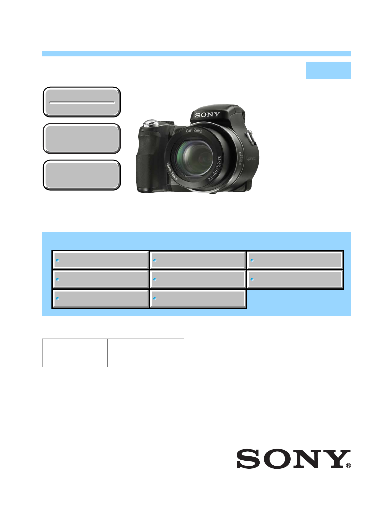
Photo: DSC-H7 Black Model
Link
Link
LEVEL 2
US Model
Canadian Model
AEP Model
UK Model
E Model
Australian Model
Hong Kong Model
Chinese Model
Korea Model
Argentine Model
Brazilian Model
Tourist Model
Japanese Model
SPECIFICATIONS
SERVICE NOTE
DISASSEMBLY
• Precaution on Replacing the SY-177 Board
The components identified by
mark 0 or dotted line with
mark 0 are critical for safety.
Replace only with part number specified.
Les composants identifiés par une
marque 0 sont critiques pour la
sécurité.
Ne les remplacer que par une pièce
portant le numéro spécifié.
BLOCK DIAGRAMS
FRAME SCHEMATIC DIAGRAMS
SCHEMATIC DIAGRAMS
PRINTED WIRING BOARDS
REPAIR PARTS LIST
DIGITAL STILL CAMERA
DSC-H7/H9_L2
9-852-203-31
Sony EMCS Co.
2007D0200-1
© 2007.4
Published by Kohda TEC
Page 2

SPECIFICATIONS
Camera
[System]
Image device: 7.18 mm (1/2.5 type) color CCD, Primary color filter
Total pixel number of camera:
Approx. 8 286 000 pixels
Effective pixel number of camera:
Approx. 8 083 000 pixels
Lens: Carl Zeiss Vario-Tessar 15× zoom lens f =5.2 – 78 mm
(31 – 465 mm when converted to a 35 mm still camera)
F2.7 – 4.5
Exposure control: Automatic exposure, Shutter speed priority,
Aperture priority, Manual exposure, Scene Selection
(9 modes)
White balance: Automatic, Daylight, Cloudy, Fluorescent 1,2,3,
Incandescent, Flash, One push
File format (DCF compliant):
Still images:Exif Ver. 2.21 JPEG compliant,
DPOF compatible
Movies: MPEG1 compliant (Monaural)
Recording media: Internal Memory (approx. 31 MB), “Memory Stick Duo”
Flash: Flash range (ISO sensitivity (Recommended exposure
value) set to ISOAUTO): approx. 0.2 to 9.8 m
(7 7/8 inches to 32 feet 1 7/8 inches) (W)/
approx. 1.2 to 6.0 m (3 feet 11 1/4 inches to 19 feet
8 1/4 inches) (T)
Viewfinder: Electric viewfinder (color)
[Input and Output connectors]
Multi connector Video output
Audio output (Monaural)
USB communication
USB communication:
Hi-Speed USB (USB 2.0 compliant)
[LCD screen]
LCD panel: DSC-H9: 7.5 cm (3.0 type) TFT drive
DSC-H7: 6.2 cm (2.5 type) TFT drive
Total number of dots:
DSC-H9: 230 400 (960 × 240) dots
DSC-H7: 115 200 (480 °— 240) dots
[Finder]
Panel: 0.5 cm (0.2 type) color
Total number of dots:
Approx. 200 000 dots equivalent
[Power, general]
Power: Rechargeable battery pack NP-BG1, 3.6 V
AC-LS5K AC Adaptor (not supplied), 4.2 V
Power consumption (during shooting with the LCD screen):
DSC-H9: 1.2 W
DSC-H7: 1.1 W
Operating temperature:
0 to 40°C (32 to 104°F)
Storage temperature:
–20 to +60°C (–4 to +140°F)
Dimensions: 109.5 × 83.4 × 85.7 mm (4 3/8 × 3 3/8 × 3 3/8 inches)
(W/H/D, excluding protrusions) (for both DSC-H9 and DSC-H7)
Mass: DSC-H9: Approx. 546 g (1 lb 3.3 oz)
(including NP-BG1 battery pack, shoulder strap, adaptor ring,
lens hood and lens cap, etc.)
DSC-H7: Approx. 514 g (1 lb 2.1 oz)
(including NP-BG1 battery pack, shoulder strap, adaptor ring,
lens hood and lens cap, etc.)
Microphone: Monaural
Speaker: Monaural
Exif Print: Compatible
PRINT Image Matching III:
Compatible
PictBridge: Compatible
BC-CSG/BC-CSGB/BC-CSGC battery charger
Power requirements:
AC 100 V to 240 V, 50/60 Hz, 2 W (BC-CSG/BC-CSGC)/
2.6 W (BC-CSGB)
Output voltage: DC 4.2 V, 0.25 A
Operating temperature:
0 to 40°C (32 to 104°F)
Storage temperature:
-20 to +60°C (–4 to +140°F)
Dimensions: Approx. 62 × 24 × 91 mm (2 1/2 × 31/32 × 3 5/8 inches) (W/H/D)
Mass: Approx. 75 g (2.7 oz)
Rechargeable battery pack NPBG1
Used battery: Lithium-ion battery
Maximum voltage:DC 4.2 V
Nominal voltage: DC 3.6 V
Capacity: 3.4 Wh (960 mAh)
Design and specifications are subject to change without notice.
DSC-H7/H9_L2
— 2 —
Page 3
Model information table
Model DSC-H7/Silver DSC-H7/Black DSC-H9/Silver DSC-H9/Black
Destination
LCD
CK board
MS board
PL board
SW board
•Abbreviation
AR : Argentine model
AUS: Australian model
BR : Brazilian model
CH : Chinese model
CND: Canadian model
US, CND, AEP, UK,
E, AUS, HK, CH,
KR, AR, J, JE
2.5 inch
CK-180, CK-181
MS-364
PL-046
SW-500
HK : Hong Kong model
J: Japanese model
JE : Tourist model
KR : Korea model
US, CND, AEP, UK,
E, AUS, HK, CH,
KR, J, JE
2.5 inch
CK-180, CK-181
MS-364
PL-046
SW-500
US, CND, AEP, UK,
E, AUS, HK, CH,
KR, JE
3.0 inch
CK-179, CK-182
MS-366
PL-047
SW-499
US, CND, AEP, UK,
E, AUS, HK, CH,
KR, AR, BR, JE
3.0 inch
CK-179, CK-182
MS-366
PL-047
SW-499
COMPONENTS IDENTIFIED BY MARK 0 OR DO TTED LINE WITH
MARK 0 ON THE SCHEMATIC DIAGRAMS AND IN THE PARTS
LIST ARE CRITICAL TO SAFE OPERATION. REPLACE THESE
COMPONENTS WITH SONY PARTS WHOSE PART NUMBERS
APPEAR AS SHOWN IN THIS MANUAL OR IN SUPPLEMENTS
PUBLISHED BY SONY .
1. Check the area of your repair for unsoldered or poorly-soldered
connections. Check the entire board surface for solder splashes
and bridges.
2. Check the interboard wiring to ensure that no wires are
"pinched" or contact high-wattage resistors.
3. Look for unauthorized replacement parts, particularly
transistors, that were installed during a previous repair. Point
them out to the customer and recommend their replacement.
4. Look for parts which, through functioning, show obvious signs
of deterioration. Point them out to the customer and
recommend their replacement.
5. Check the B+ voltage to see it is at the values specified.
6. FLEXIBLE Circuit Board Repairing
•Keep the temperature of the soldering iron around 270°C
during repairing.
•Do not touch the soldering iron on the same conductor of the
circuit board (within 3 times).
•Be careful not to apply force on the conductor when soldering
or unsoldering.
DSC-H7/H9_L2
Danger of explosion if battery is incorrectly replaced.
CAUTION
Replace only with the same or equivalent type.
SAFETY-RELATED COMPONENT WARNING!!
SAFETY CHECK-OUT
After correcting the original service problem, perform the following
safety checks before releasing the set to the customer.
ATTENTION AU COMPOSANT AYANT RAPPORT
À LA SÉCURITÉ!
LES COMPOSANTS IDENTIFÉS P AR UNE MARQUE 0 SUR LES
DIAGRAMMES SCHÉMA TIQUES ET LA LISTE DES PIÈCES SONT
CRITIQUES POUR LA SÉCURITÉ DE FONCTIONNEMENT. NE
REMPLACER CES COMPOSANTS QUE PAR DES PIÈSES SONY
DONT LES NUMÉROS SONT DONNÉS DANS CE MANUEL OU
DANS LES SUPPÉMENTS PUBLIÉS PAR SONY.
Unleaded solder
Boards requiring use of unleaded solder are printed with the leadfree mark (LF) indicating the solder contains no lead.
(Caution: Some printed circuit boards may not come printed with
the lead free mark due to their particular size.)
: LEAD FREE MARK
Unleaded solder has the following characteristics.
• Unleaded solder melts at a temperature about 40°C higher than
ordinary solder.
Ordinary soldering irons can be used but the iron tip has to be
applied to the solder joint for a slightly longer time.
Soldering irons using a temperature regulator should be set to
about 350°C.
Caution: The printed pattern (copper foil) may peel away if the
heated tip is applied for too long, so be careful!
• Strong viscosity
Unleaded solder is more viscous (sticky, less prone to flow) than
ordinary solder so use caution not to let solder bridges occur such
as on IC pins, etc.
• Usable with ordinary solder
It is best to use only unleaded solder but unleaded solder may
also be added to ordinary solder.
— 3 —
Page 4

TABLE OF CONTENTS
Section Title Page Section Title Page
1. SERVICE NOTE
1-1. Precaution on Replacing the SY-177 Board ····················1-1
1-2. Description on Self-diagnosis Display···························· 1-1
1-3. Process After Fixing Flash Error ·····································1-1
1-4. Method for Copying or Erasing the Data in Internal
Memory ···········································································1-2
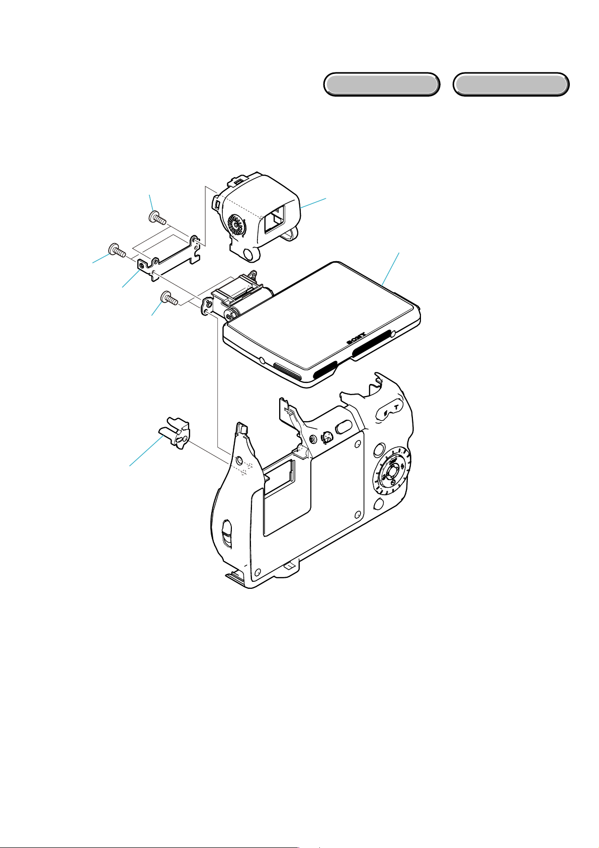
2. DISASSEMBLY
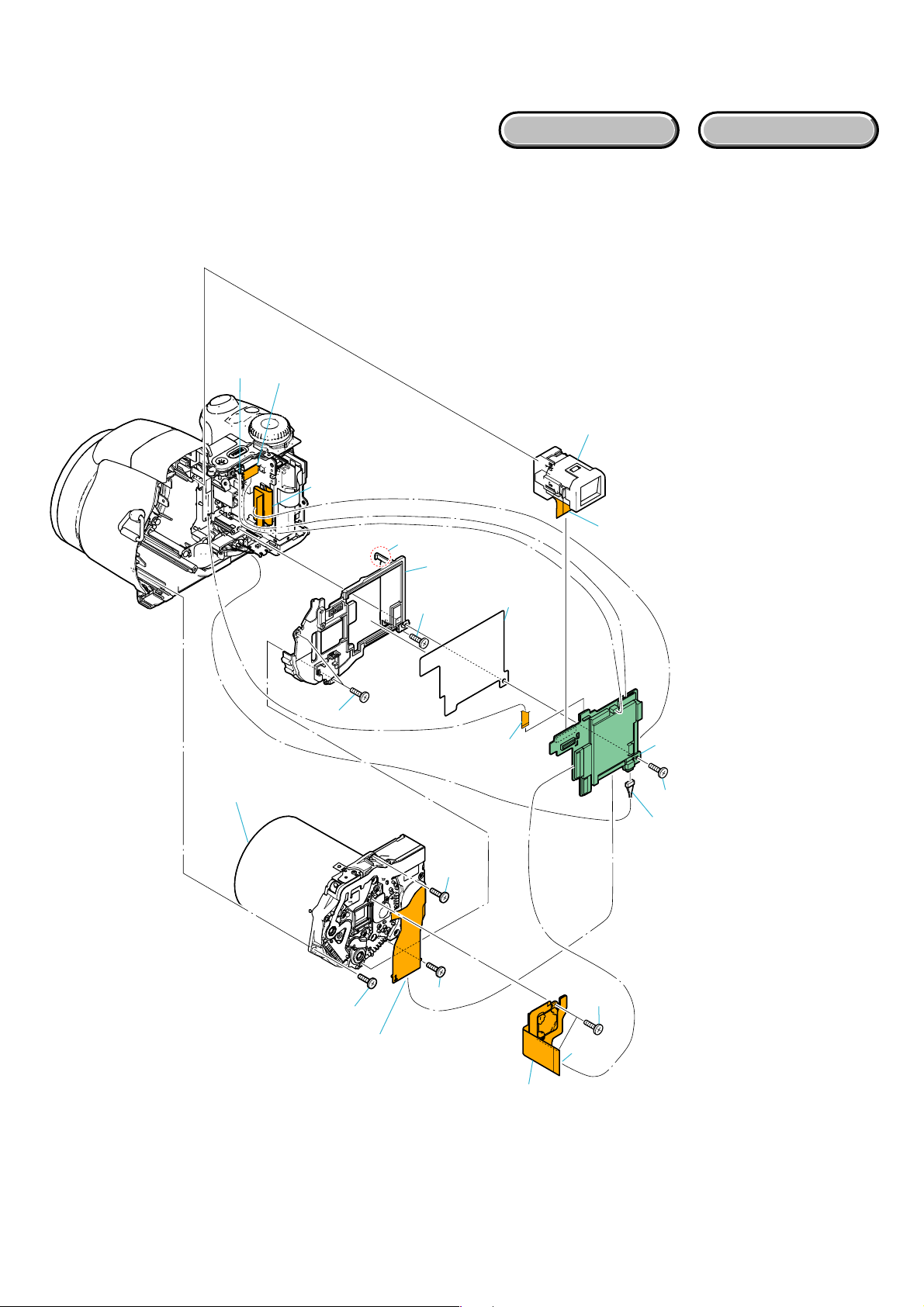
2-1. Disassembly····································································· 2-2
3. BLOCK DIAGRAMS
3-1. Overall Block Diagram (1/2)···········································3-1
3-2. Overall Block Diagram (2/2)···········································3-2
3-3. Power Block Diagram (1/2) ············································3-3
3-4. Power Block Diagram (2/2) ············································3-4
4. PRINTED WIRING BOARDS AND
SCHEMATIC DIAGRAMS
4-1. Frame Schematic Diagram ··············································4-1
4-2. Schematic Diagrams························································4-2
4-3. Printed Wiring Boards ···················································4-22
5. REPAIR PARTS LIST
5-1. Exploded V iews ·······························································5-2
5-2. Electrical Parts List ·························································5-7
DSC-H7/H9_L2
— 4 —
Page 5
ENGLISH JAPANESE
ENGLISH JAPANESE
1. SERVICE NOTE
1-1. PRECAUTION ON REPLACING THE SY-177 BOARD
DESTINATION DATA
When you replace to the repairing board, the written destination data of repairing board also might be changed to original setting.
Refer to Service Manual ADJ, and perform “DESTINATION DATA WRITE”.
USB SERIAL No.
The set is shipped with a unique ID (USB Serial No.) written in it.
This ID has not been written in a new board for service, and therefore it must be entered after the board replacement.
Refer to Service ManualADJ, and perform “USB SERIAL No. INPUT”.
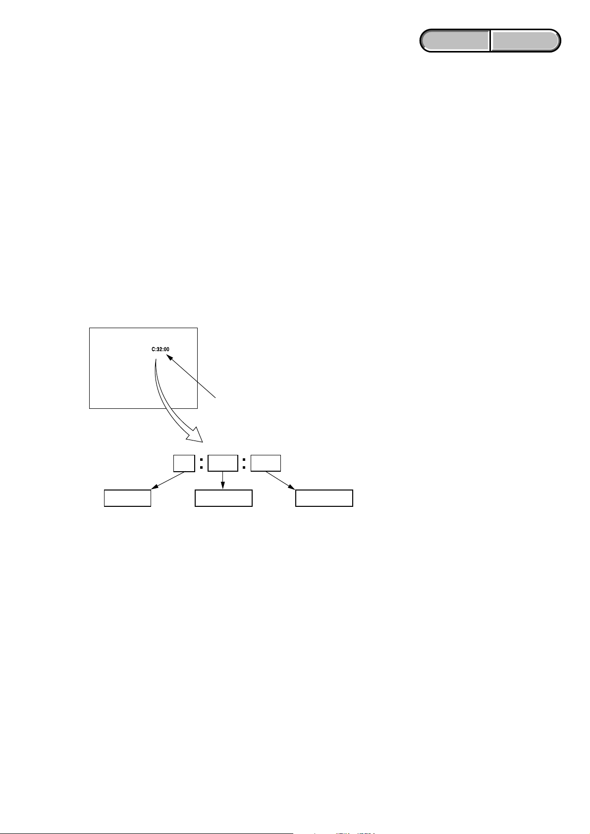
1-2. SELF-DIAGNOSIS FUNCTION
1-2-1. Self-diagnosis Function
When problems occur while the unit is operating, the self-diagnosis
function starts working, and displays on the LCD screen what to
do.
Details of the self-diagnosis functions are provided in the Instruction
manual.
LCD screen
Blinks at 3.2 Hz
0 0
Detailed Code
Refer to “1-2-3. Self-diagnosis Code Table”.
Repaired by:
C : Corrected by customer
E : Corrected by service
engineer
3 2C
Block
Indicates the appropriate
step to be taken.
E.g.
13 ....Format the “Memory Stick Duo”.
32 ....Turn on power again.
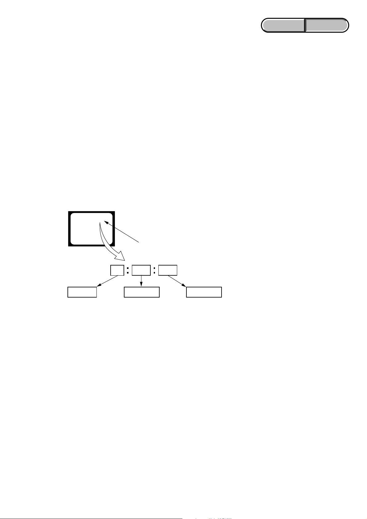
1-2-2. Self-diagnosis Display
When problems occur while the unit is operating, the LCD screen
shows a 4-digit display consisting of an alphabet and numbers, which
blinks at 3.2 Hz. This 5-character display indicates the “repaired
by:”, “block” in which the problem occurred, and “detailed code”
of the problem.
DSC-H7/H9_L2
1-1
Page 6
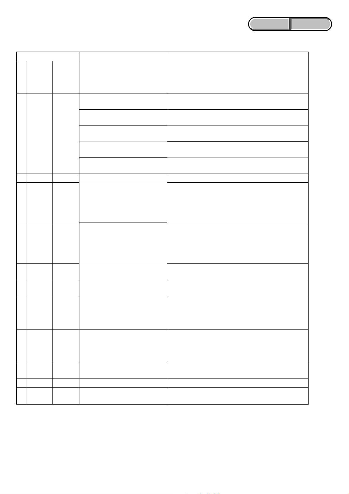
1-2-3. Self-diagnosis Code Table
Self-diagnosis Code
ENGLISH JAPANESE
ENGLISH JAPANESE
Function
Repaired by:
C
C
Block
13
32
Detailed
Code
01
01
Symptom/State
The internal memory has experienced a
format error.
“Memory Stick Duo” is unformatted.
“Memory Stick Duo” is broken.
“Memory Stick Duo” type error
The camera cannot read or write data
on the “Memory Stick Duo”.
Trouble with hardware
Format the internal memory.
Format the “Memory Stick Duo”.
Insert a new “Memory Stick Duo”.
Insert a supported “Memory Stick Duo”.
Turn the power off and on again, or taking out and inserting the
“Memory Stick Duo” several times.
Turn the power off and on again.
Retry turn the power on by the power switch. If it does not
E
61
01
Difficult to adjust focus
(Cannot initialize focus)
recover, check the focus reset sensor of lens block (pin wj of
CN401 on the SY-177 board). If it is OK, check the focus motor
drive IC (IC401 on the SY-177 board).
Retry turn the power on by the power switch. Check the zoom
reset sensor of lens block (pin qj of CN401 on the SY-177
board), if zooming is performed when the zoom button is
operated. If it is OK, check the zoom motor drive IC (IC401 on
E
61
02
Zoom operations fault
(Cannot initialize zoom lens.)
the SY-177 board).
E
E
62
62
02
10
Abnormality of IC for steadyshot.
Lens initializing failure.
Check or replacement of the IC for steadyshot (IC503 on the SY177 board).
Check or replacement of the IC for steadyshot (IC503 on the SY177 board).
Check the HALL element (PITCH) of optical image stabilizer
E
62
11
Lens overheating (PITCH).
(pin eg, ej of CN401 on the SY-177 board). If it is OK, check
PITCH angular velocity sensor (SE501 on the SY-177 board)
peripheral circuits.
Check the HALL element (YAW) of optical image stabilizer (pin
E
62
12
Lens overheating (YAW).
e;, es of CN401 on the SY-177 board). If it is OK, check YAW
angular velocity sensor (SE502 on the SY-177 board) peripheral
circuits.
E
E
E
62
91
92
20
01
00
Abnormality of thermistor.
Abnormality when flash is being charged.
Non-standard battery is used.
Check the OIS temp sensor of optical image stabilizer (pin ef of
CN401 on the SY-177 board).
Checking of flash unit or replacement of flash unit. (Note)
Use the compatible battery only.
Note: After repair, be sure to perform “1-3. PROCESS AFTER FIXING FLASH ERROR”.
Correction
1-3. PROCESS AFTER FIXING FLASH ERROR
When “FLASH error” (Self-diagnosis Code E : 91 : 01) occurs, to prevent any abnormal situation caused by high voltage, setting of the flash
is changed automatically to disabling charge and flash setting.
After fixing, this setting needs to be deactivated. Flash error code can be initialized by the operations on the HOME screen.
Method for Initializing the Flash Error Code
Initialize
Initializes the setting to the default setting. Even if you execute this function, the images
stored in the internal memory are retained.
1 Select [Initialize] with v/V/b/B, then press z.
The message “Initialize all settings” appears.
2 Select [OK] with v, then press z.
The settings are reset to the default setting.
To cancel the resetting
Select [Cancel] in step 2, then press z.
•Make sure that the power is not disconnected during resetting.
DSC-H7/H9_L2
1-2
Page 7

ENGLISH JAPANESE
ENGLISH JAPANESE
1-4. METHOD FOR COPYING OR ERASING THE DATA IN INTERNAL MEMORY
The data can be copied/erased by the operations on the HOME screen. (When erasing the data, execute formatting the internal memory.)
Note: When replacing the SY-177 board, erase the data in internal memory of the board before replacement.
Method for Copying the Data in Internal Memory
Copy
Copies all images in the internal memo r y to a “Memory Stick Duo”.
1 Insert a “Memory Stick Duo” having 32 M B or larger capacit y.
2 Select [Copy] with v/V/b/B on the control button, then press z.
The message “All data in internal memory will be copied” appears.
3 Select [OK] with v, then press z.
Copying starts.
To canc el the copying
Select [Cancel] in step 3, then press z.
•Use a fully charged battery pack. If you attempt to copy image files using a battery pack with little
remaining charge, the battery pack may run out, causing copying to fail or possibly corrupting the data.
•You cannot copy individual images.
•The original images in the internal memory are retained even after copying. To delete the contents of the
internal memory, remove the “Memory Stick Duo” after copying, then execute the [Format] command in
[ Internal Memory Tool] .
•When you copy the data in the internal memory to the “Memory Stick Duo”, all the data will be copied.
You cannot choose a specific folder on the “Memory Stick Duo” as the destination for the data to be
copied.
•Even if you copy data, a DPOF (Print order) mark is not copied.
Method for Formatting the Internal Memory
This item does not appear when a “Memory Stick Duo” is inserted in the camera.
Format
Formats the internal memory.
•Note that formatting irrevocably erases all data in the internal memory, including even protected images.
1 Select [Format] with v/V/b/B on the control button, then press z.
The message “All data in internal memory will be erased” appears.
2 Select [OK] with v, then press z.
The format is completed.
To cancel the formatting
Select [Cancel] in step 2, then press z.
DSC-H7/H9_L2
1-3
Page 8
ENGLISH JAPANESE
ENGLISH JAPANESE
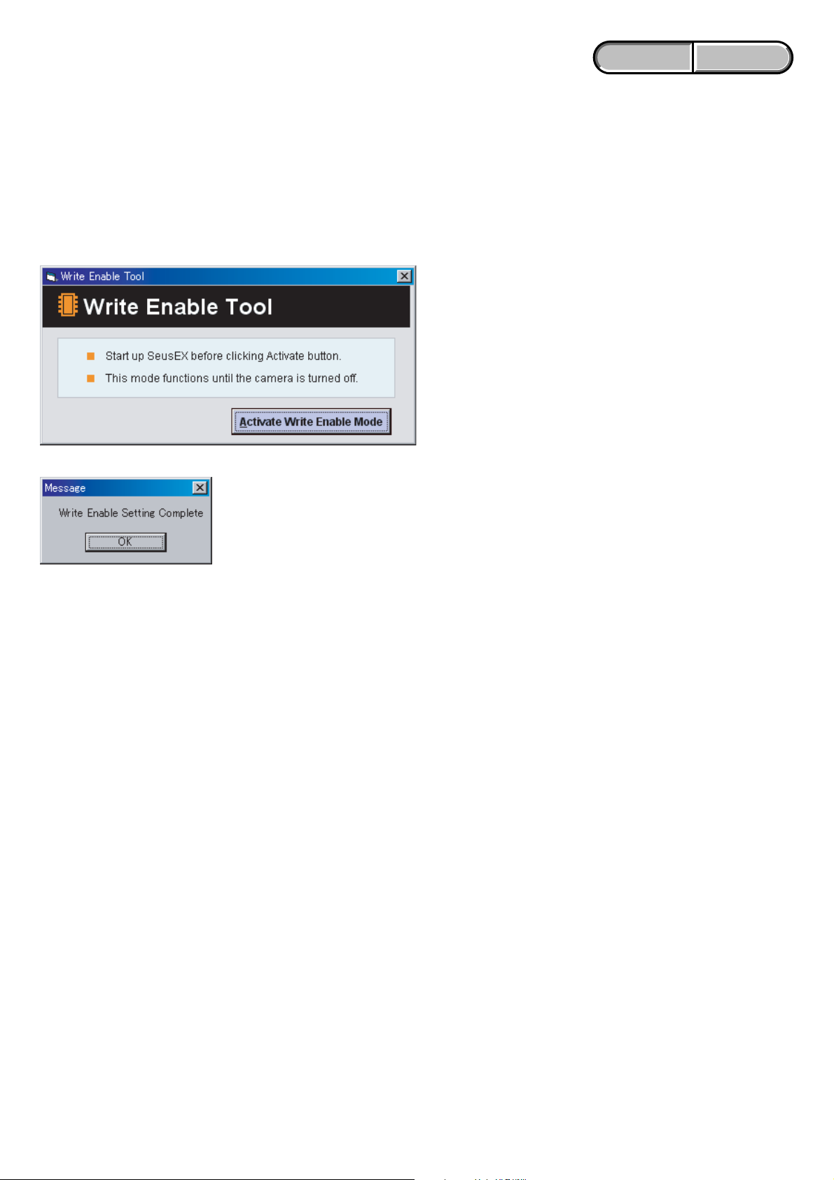
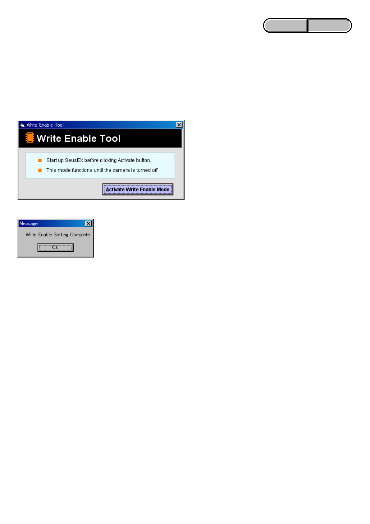
1-5. HOW TO WRITE DATA TO INTERNAL MEMORY
Usually, the camera has been set so as to disable the data writing from the PC to the internal memory of the camera.
This setting must be changed temporarily when the data is to be written to the internal memory such as a case after the board replacement.
To change the setting, use the write enable tool “WriteEnableTool.exe”.
Data writing method
1) Connect the PC to the camera (USB mode: Mass Storage), and switch the driver to the “Sony Seus USB Driver”.
2) Start the Write Enable Tool and the SeusEX.
3) Click the button of the Write Enable Tool.
4) Upon completion of the setting change, the following message will be displayed.
[Activate Write Enable Mode]
5) Return the driver to the original one, and connect the PC to the camera (USB mode: Mass Storage).
6) Write the data read out into the PC to the internal memory of the camera.
7) Disconnect the PC from the camera, and turn off the camera.
Note: By turning off the camera, the write enable setting is reset.
DSC-H7/H9_L2
1-4
Page 9
ENGLISH JAPANESE
ッ
の
ENGLISH JAPANESE
1.サービスノート
1-1. SY-177基板交換時の注意
仕向けデータ
補修用基板と交換する時,補修用基板に書かれている仕向けデータは元の設定と違っている場合があります。
ADJ編を参照して,「DESTINATIONDATAWRIT E」を行ってください。
USBシリアルNo.
セットは,1台毎に異なる固有のID(USBSerealNo.)を書き込んだ後,出荷されています。
新品の補修用基板には,このIDが書き込まれていないので,基板交換後にIDを入力する必要があります。
ADJ編を参照して,「USBSERIA LNo.INP UT」を行ってください。
1-2. 自己診断機能
1-2-1. 自己診断機能について
本機の動作に不具合が生じたとき,自己診断機能が働き,
LCD画面に,どう処置したらよいか判断できる表示を行い
ます。自己診断機能については取扱説明書にも掲載されて
います。
1-2-2. 自己診断表示
本機の動作に不具合が生じたとき,LCD画面にアルファベ
トと4桁の数字が表示され,3. 2H zで点滅します。この5文字
の表示によって対応者分類および不具合の生じたブロック
分類,不具合の詳細コードを示します。
LCD画面
C : 3 2 : 00
3.2Hz点滅
3 2C
対応者分類
C :お客さま自身で対応
E :サービスエンジニア
で対応 デュオ”をフォーマッ
ブロック分類
対応方法の違いにより分類
例 13・・・“メモリースティック
トする
32・・・電源を入れ直す
0 0
詳細コード
「1-2-3 . 自己診断コード表」
を参照
DSC-H7/H9_L2
1-5
Page 10
1-2-3. 自己診断コード表
自己診断コード
対
応
者
ブロック
機能
詳細
コード
症状/状態
対応/方法
ENGLISH JAPANESE
ENGLISH JAPANESE
C
C
E
E
E
E
E
E
E
E
E
13
32
61
61
62
62
62
62
62
91
92
01
01
01
02
02
10
11
12
20
01
00
内蔵メモリにフォーマットエラーが
あった。
フォーマットしていないメモリー
スティックデュオを入れた。
メモリースティックデュオが
壊れている。
メモリースティックデュオの
タイプエラーを検出した。
メモリースティックデュオが
読み/書きできない。
ハードウェアトラブルを検出した。
フォーカスが合いにくい。
(フォーカスの初期化ができない)
ズーム動作の異常。
(ズームレンズの初期化ができな
い)
手振れ補正用ICの異常。
手振れ補正用ICの異常。
(レンズ初期化異常)
レンズオーバーヒート(PITCH)
レンズオーバーヒート(YAW)
サーミスタの異常。
フラッシュの充電異常。
規定外の充電池が使用された。
内蔵メモリをフォーマットする。
メモリースティックデュオをフォーマットする。
新しいメモリースティックデュオに交換する。
規格内のメモリースティックデュオを挿入する。
電源の入れ直し,またはメモリースティックデュオ
の挿し/外しを数回試す。
電源を入れ直す。
操作スイッチの電源を入れ直す。
復帰しない場合はレンズブロックのフォーカスリセットセ
ンサ(SY-177基板CN401wjピン)を点検する。異常なけ
れば フォーカスモータ駆動 IC(SY-177基板IC401)を点検
する。
操作スイッチの電源を入れ直す。
ズームボタンを操作したときにズーム動作をすればレンズ
ブロックのズームリセットセンサ(SY-177基板CN401qj
ピン)を点検する。異常なければズームモータ駆動IC
(SY-177基板IC401)を点検する。
手振れ補正用IC(SY-177基板IC503)を点検または交換す
る。
手振れ補正用IC(SY-177基板IC503)を点検または交換す
る。
光学手振れ補正ブロックのホール素 子 (PITCH)(SY-177
基板CN401eg,ejピン)を点検する。異常なければ
PITCH角速度センサ(SY-177基板SE501)周辺の回路を点
検する。
光学手振れ補正ブロックのホール素 子 (YAW)(SY-177
基板CN401e;,esピン)を点検する 。異常なければYAW
角速度センサ(SY-177基板SE502)周辺の回路を点検す
る。
光学手振れ補正ブロックの サーミスタ(SY-177基板CN401
efピン)を点検する。
フラッシュユニットを点検または交換する。(Note)
規定の充電池を使用する。
Note:交換後は,必ず「1-3.フラッシュ異常修理後の処置」を行って下さい。
DSC-H7/H9_L2
1-6
Page 11
ENGLISH JAPANESE
ュ
よ
ま
ENGLISH JAPANESE
1-3. フラッシュエラー発生時の対処法
本機はフラッシュエラー(自己診断コードE:91:0 1)が発生した場合,高電圧による異常を防止するために自動的にフラッシ
充電および発光禁止の設定になります。
フラッシュエラー発生後はエラーの解除を行う必要があります。エラーの解除はホーム画面から初期化操作を実行することに
り行います。
設定リセット
お買い上げ時の設定に戻します。
[設定リセット]を実行しても、内蔵メモリーに記録されている画像は削除されません。
1
コントロールボタンの
「全ての設定内容をリセットします」というメッセージが表示される。
2
で[実行]を選び、中央の を押す。
設定リセットが実行される。
設定リセットを中止するには
2
手順 で、[キャンセル]を選び、中央の を押す。
設定リセット中は電源が切れないようにご注意ください。
で[設定リセット]を選び、中央の を押す。
/ / /
1-4. 内蔵メモリのデータコピーおよび消去方法
内蔵メモリのデータコピーまたは消去はホーム画面の操作から実行可能です。(消去する場合は内蔵メモリの初期化を行い
す。)
Note:SY-177基板交換の際は,基板交換前に内蔵メモリのデータを消去して下さい。
内蔵メモリのコピー方法
コピー
内蔵メモリーに記録した画像を、メモリースティックデュオに一括コピーします。
1
2
3
以上の容量のあるメモリースティックデュオを本体に入れる。
32MB
b
コントロールボタンのv
「内蔵メモリーのデータがすべてコピーされます」というメッセージが表示される。
v で[実行]を選び、中央のz を押す。
コピーが実行される。
で[コピー]を選び、中央のz を押す。
/V/B/
コピーを中止するには
手順3で、[キャンセル]を選び、中央のzを押す。
充分に充電したバッテリーをご使用ください。残量の少ないバッテリーを使用して画像ファイ
∗
ルをコピーすると、バッテリー切れのため、データを転送できなかったり、データを破損するお
それがあります。
画像ごとのコピーはできません。
∗
データをコピーしても、内蔵メモリー内のデータは削除されません。内蔵メモリーの内容を消
∗
去するには、コピー後にメモリースティックデュオを本体から取りはずし、[
リーツール]の[フォーマット]を行ってください。
データをコピーすると、メモリー ス ティックデュオ 内に新しいフォルダが作成されます。
∗
コピー先のフォルダを指定することはできません。
データのコピーを行っても、
∗
(プリント予約)マークの設定はコピーされません。
DPOF
内蔵メモ
内蔵メモリのフォーマット方法
“メモリースティックデュオ”が本機に入っている場合は表示されません。
フォーマット
内蔵メモリーの管理領域をフォーマット(初期化)します。
フォーマットすると、プロテクトしてある画像も含めて、すべてのデータが消去され、元に戻せ
ません。
1
コントロールボタンの
「内蔵メモリーのデータがすべて消去されます」というメッセージが表示される。
で[実行]を選び、中央の を押す。
フォーマットが実行される。
2
フォーマットを中止するには
手順 で、[キャンセル]を選び、中央の を押す。
2
で[フォーマット]を選び、中央の を押す。
/ / /
DSC-H7/H9_L2
1-7
Page 12
1-5. 内蔵メモリへデータを書き戻す方法
。
通常は,PCからカメラの内蔵メモリへデータを書き込むことはできない設定になっています。
基板交換後などに,内蔵メモリへデータを書き戻す場合には,この設定を一時的に変更する必要があります
設定の変更には,書き込み許可ツール(WriteEnableTool.exe)を使用します。
書き戻し方法
1) カメラとPCをマスストレージ接続し,ドライバを"SonySeusUSBDriver"に切り替える。
2) 書き込み許可ツールとSeusEXを起動する。
3) 書き込み許可ツールの[Activate Write Enable Mode]ボタンをクリックする。
ENGLISH JAPANESE
ENGLISH JAPANESE
4) 設定の変更が終了すると,次のメッセージが表示されます。
5) ドライバを元に戻して、カメラとPCをマスストレージ接続する。
6) PCに読み出しておいたデータをカメラの内蔵メモリに書き込む。
7) カメラとPCの接続を解除し,カメラの電源をOFFにする。
注意:カメラの電源をOFFにすることにより,書き込み許可の設定が解除されます。
DSC-H7/H9_L2
1-8
Page 13
NOTE FOR REPAIR
2. DISSASSEMBLY
• Make sure that the flat cable and flexible board are not cracked of bent at the terminal.
Do not insert the cable insufficiently nor crookedly.
• When remove a connector, dont’ pull at wire of connector. It is possible that a wire is snapped.
• When installing a connector, dont’ press down at wire of connector.
It is possible that a wire is snapped.
• Do not apply excessive load to the gilded flexible board.
Cut and remove the part of gilt
which comes off at the point.
(Be careful or some
pieces of gilt may be left inside)
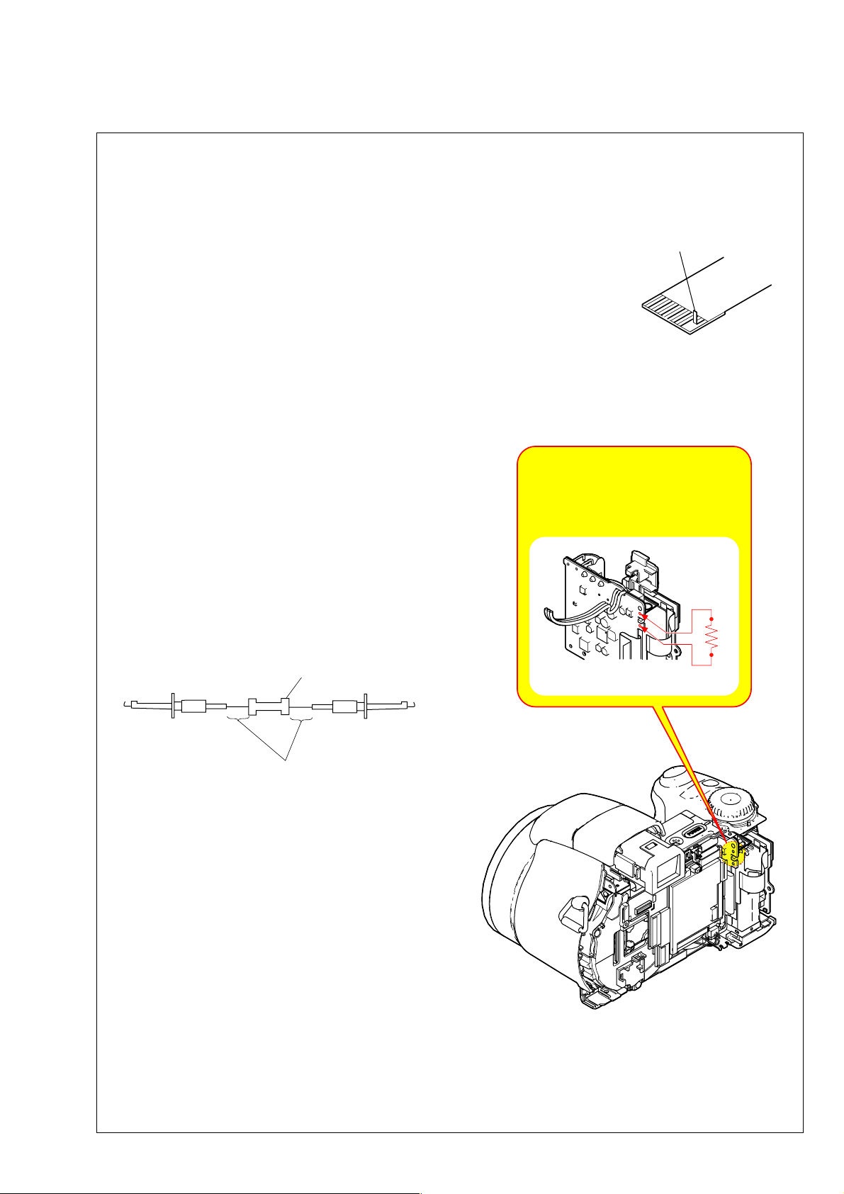
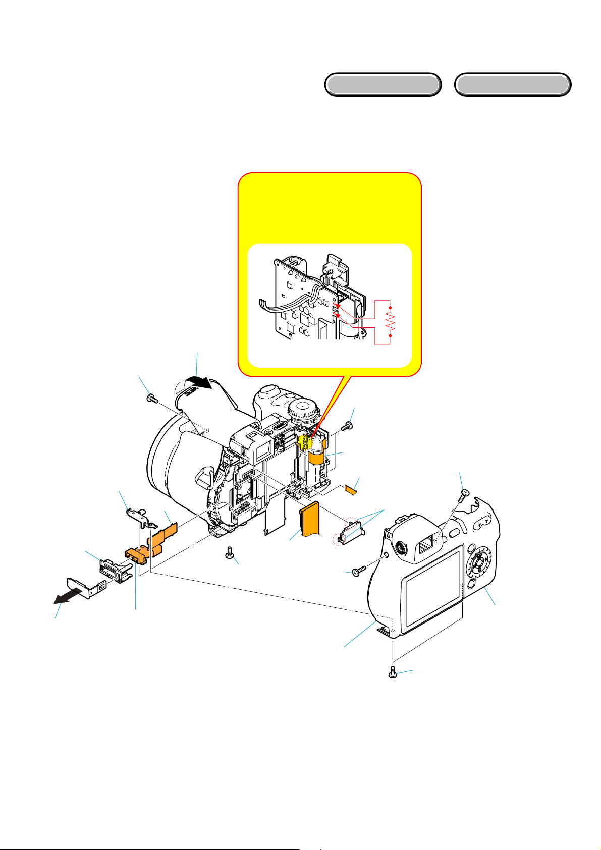
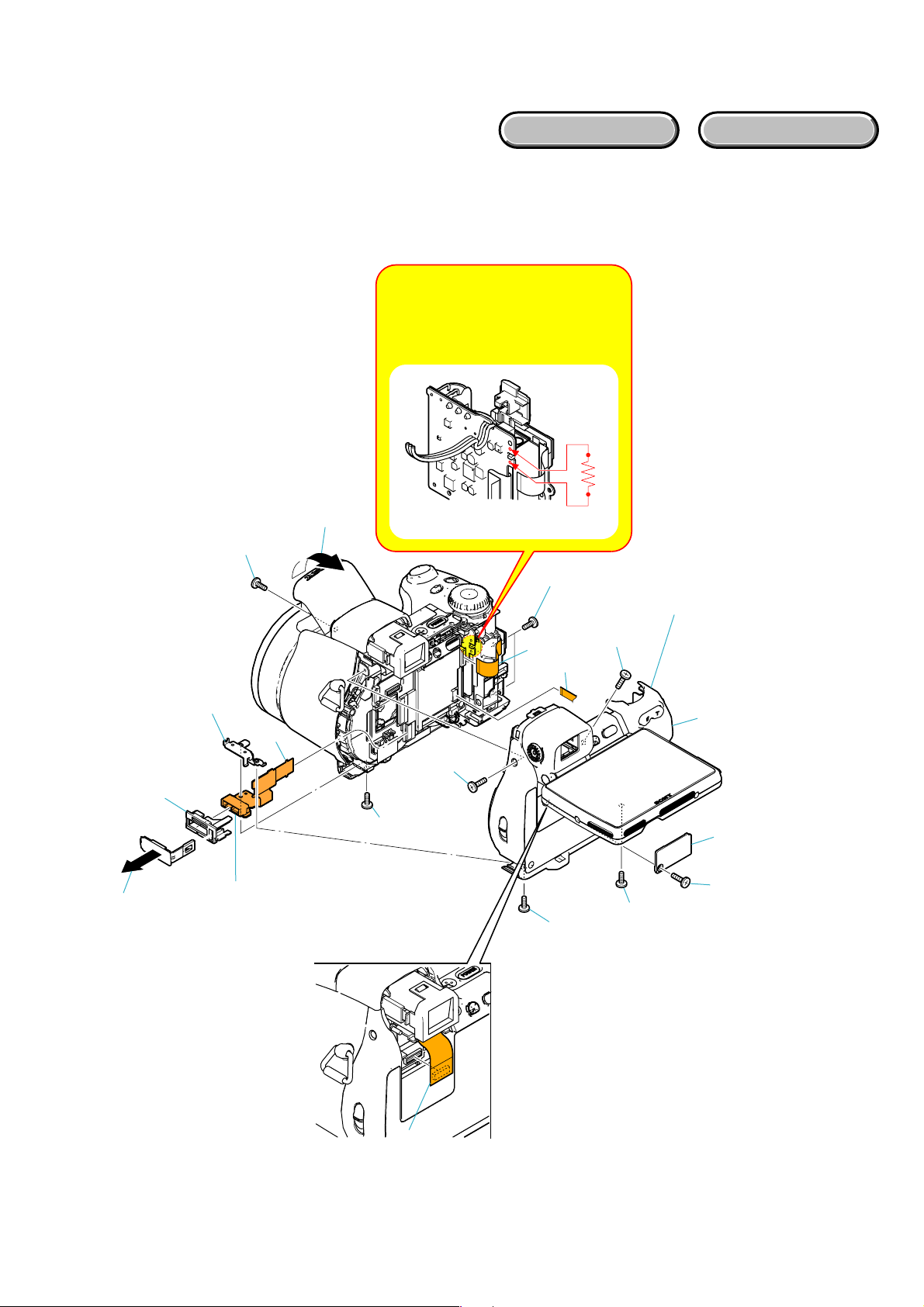
DISCHARGING OF THE DD-272 BOARD’S CHARGING CAPACIT OR (C205)
The charging capacitor (C205) of the DD-272 board is charged
up to the maximum 300 V potential.
There is a danger of electric shock by this high voltage when the
capacitor is handled by hand. The electric shock is caused by
the charged voltage which is kept without discharging when the
main power of the unit is simply turned off. Therefore, the
remaining voltage must be discharged as described below.
Preparing the Short Jig
To preparing the short jig, a small clip is attached to each end of
a resistor of 1 kΩ /1 W (1-215-869-11).
Wrap insulating tape fully around the leads of the resistor to
prevent electrical shock.
Note: High-voltage cautions
Discharging the Capacitor
Short-circuit between the two points
with the short jig about 10 seconds.
1 kΩ/1 W
Wrap insulating tape.
R:1 kΩ/1 W
(Part code: 1-215-869-11)
DSC-H7/H9_L2
2-1
Page 14
2-1. DISASSEMBLY
EXPLODED VIEW
EXPLODED VIEW
2-1-1. CABINET(REAR) BLOCK ASSY AND JK-338 FLEXIBLE BOARD (DSC-H7)
Note: High-voltage cautions
Discharging the Capacitor
Short-circuit between the two points
with the short jig about 10 seconds.
HARDWARE LIST
HARDWARE LIST
1-7
2-3
1-5
1-6 (#12)
2-4
2-2
2-1(#10)
2 JK-338 Flexible Board
R:1 kΩ/1 W
(Part code: 1-215-869-11)
1-4 (#10)
1-12
1-11
1-10
1-1 (#10)
1-3 (#10)
1-9 (Claw)
1-8
DSC-H7/H9_L2
1 Cabinet (Rear) Block Assy
1-2 (#10)
2-2
Page 15
EXPLODED VIEW
EXPLODED VIEW
2-1-2. CABINET(REAR) BLOCK ASSY AND JK-338 FLEXIBLE BOARD (DSC-H9)
1 Cabinet (Rear) Block ASSY
1-1 (#10)
1-2
1-3
1-4
1-5 (#12)
1-6 (#10)
1-7 (#10)
1-8 (#10)
1-9 (#10)
1-10 (#10)
1-11
1-13
1-12
2 JK-338 Flexible Board
2-1(#10)
2-3
2-4
2-2
1-14
Note: High-voltage cautions
Discharging the Capacitor
Short-circuit between the two points
with the short jig about 10 seconds.
R:1 kΩ/1 W
(Part code: 1-215-869-11)
HARDWARE LIST
HARDWARE LIST
DSC-H7/H9_L2
2-3
Page 16
EXPLODED VIEW
EXPLODED VIEW
2-1-3. SY-177 BOARD, SY FRAME, CCD BLOCK ASSY AND LENS BLOCK ASSY
1-1
1-2
1-9
1-3
HARDWARE LIST
HARDWARE LIST
2-2 (#12)
4 Lens Block Assy
2-4 (Claw)
2 SY Frame
2-3 (#12)
4-3(#74)
2-1
(DSC-H9 only)
1-8
1-10
1 SY-177 Board
1-7 (#12)
1-6
DSC-H7/H9_L2
4-1(#74)
1-4
4-2(#74)
3 CCD Block Assy
2-4
3-1(#73)
1-5
Page 17
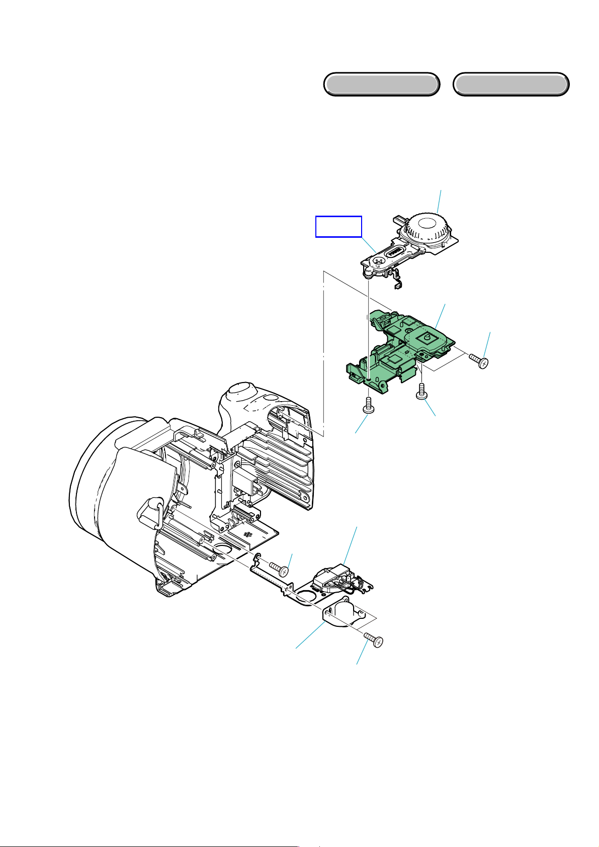
2-1-4. LOUD SPEAKER BLOCK ASSY AND MODE DIAL BLOCK ASSY
EXPLODED VIEW
EXPLODED VIEW
2 Mode Dial Block Assy
HELP
HARDWARE LIST
HARDWARE LIST
2-4
2-1(#75)
1-3(#12)
1-2
2-2(#75)
2-3(#75)
1 Loud Speaker Block Assy
1-1 (#12)
DSC-H7/H9_L2
2-5
Page 18
2-1-5. BATTERY BLOCK ASSY AND FLASH BLOCK ASSY
EXPLODED VIEW
EXPLODED VIEW
HARDWARE LIST
HARDWARE LIST
2 Flash Block Assy
HELP
2-2
2-1
2-3 (#12)
1 Battery Block Assy
DSC-H7/H9_L2
1-1 (#12)
2-6
Page 19
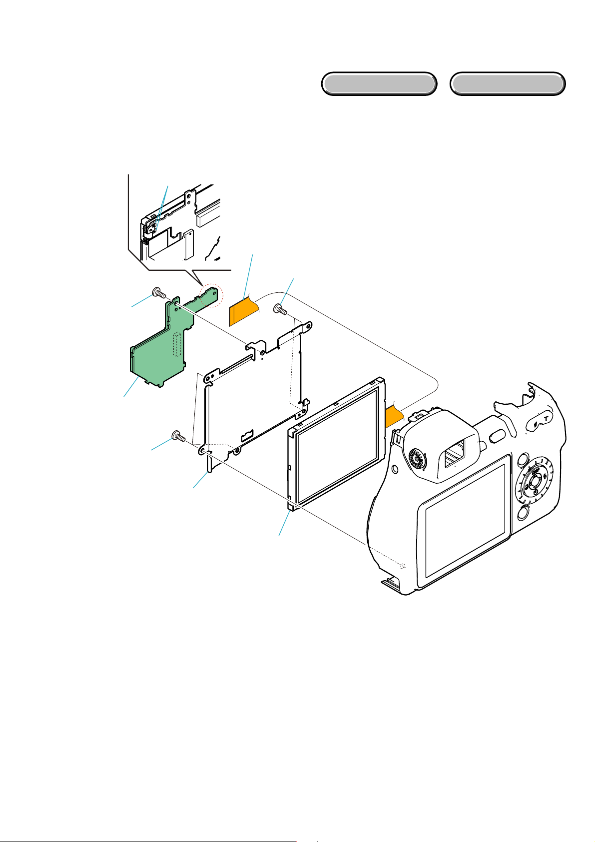
2-1-6. LCD PANEL BLOCK (DSC-H7)
EXPLODED VIEW
EXPLODED VIEW
1-2
1-3 (#10)
1-1
1-5 (#2)
HARDWARE LIST
HARDWARE LIST
1-4
1-6 (#2)
1-7
1 LCD Panel Block
DSC-H7/H9_L2
2-7
Page 20
2-1-7. LCD PANEL BLOCK (DSC-H9)
EXPLODED VIEW
EXPLODED VIEW
HARDWARE LIST
HARDWARE LIST
1-4 (#14)
1-2 (#12)
1-3
1 LCD Panel Block Assy
1-5
1-6 (#12)
1-1
DSC-H7/H9_L2
2-8
Page 21
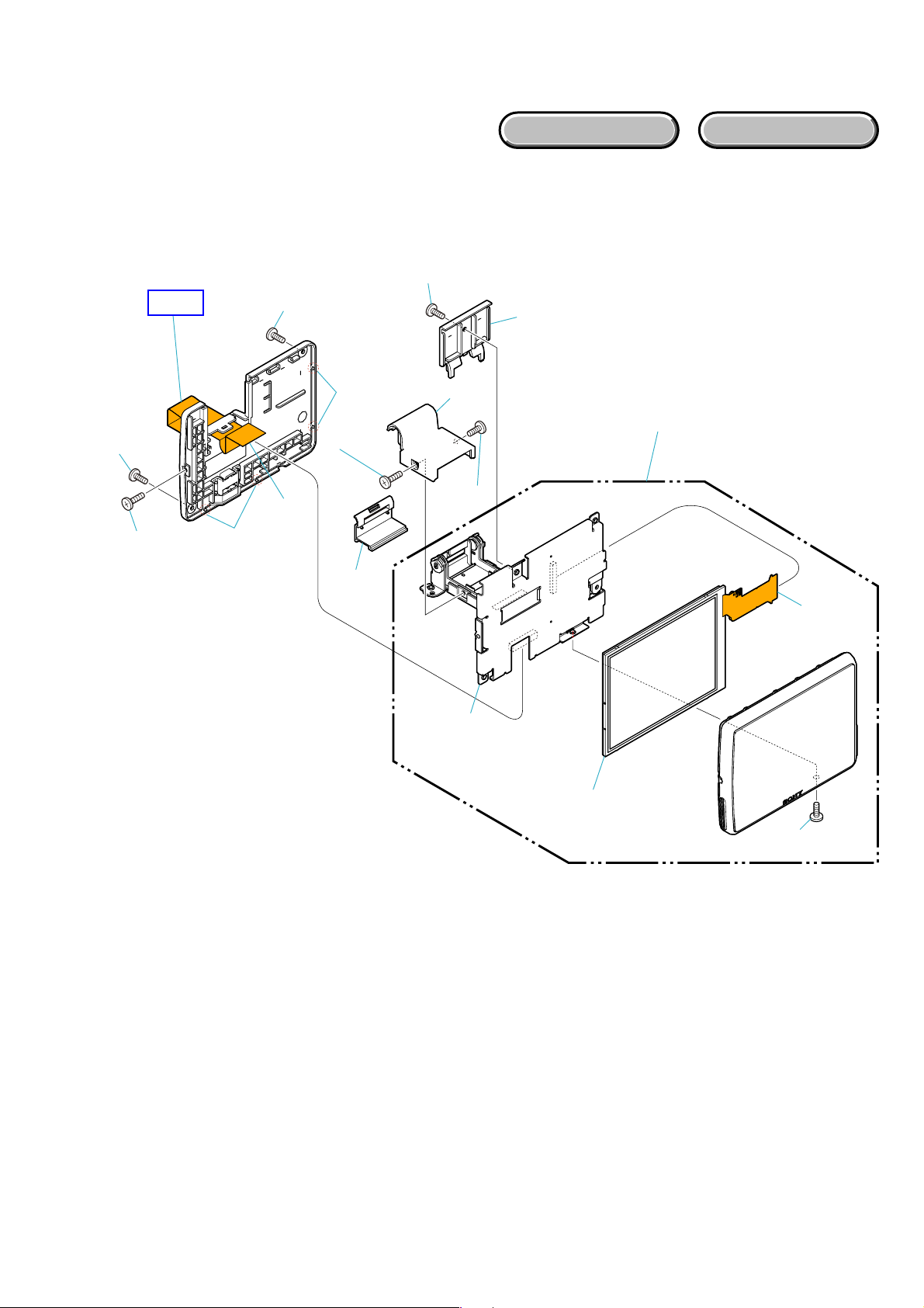
EXPLODED VIEW
EXPLODED VIEW
2-1-8. PANEL BLOCK ASSY AND LCD BLOCK ASSY (DSC-H9)
1-2 (#14)
HARDWARE LIST
HARDWARE LIST
HELP
1-8 (#14)
1-7 (#14)
1-9 (#14)
1-12
1-11 (Claw)
1-10 (Claw)
1-4 (#10)
1-1
1-3
1-6
1 Panel Block Assy
1-5 (#10)
2-1
2-3
2 LCD Block Assy
2-2 (#14)
DSC-H7_H9_L2
2-9E
Page 22
HELP
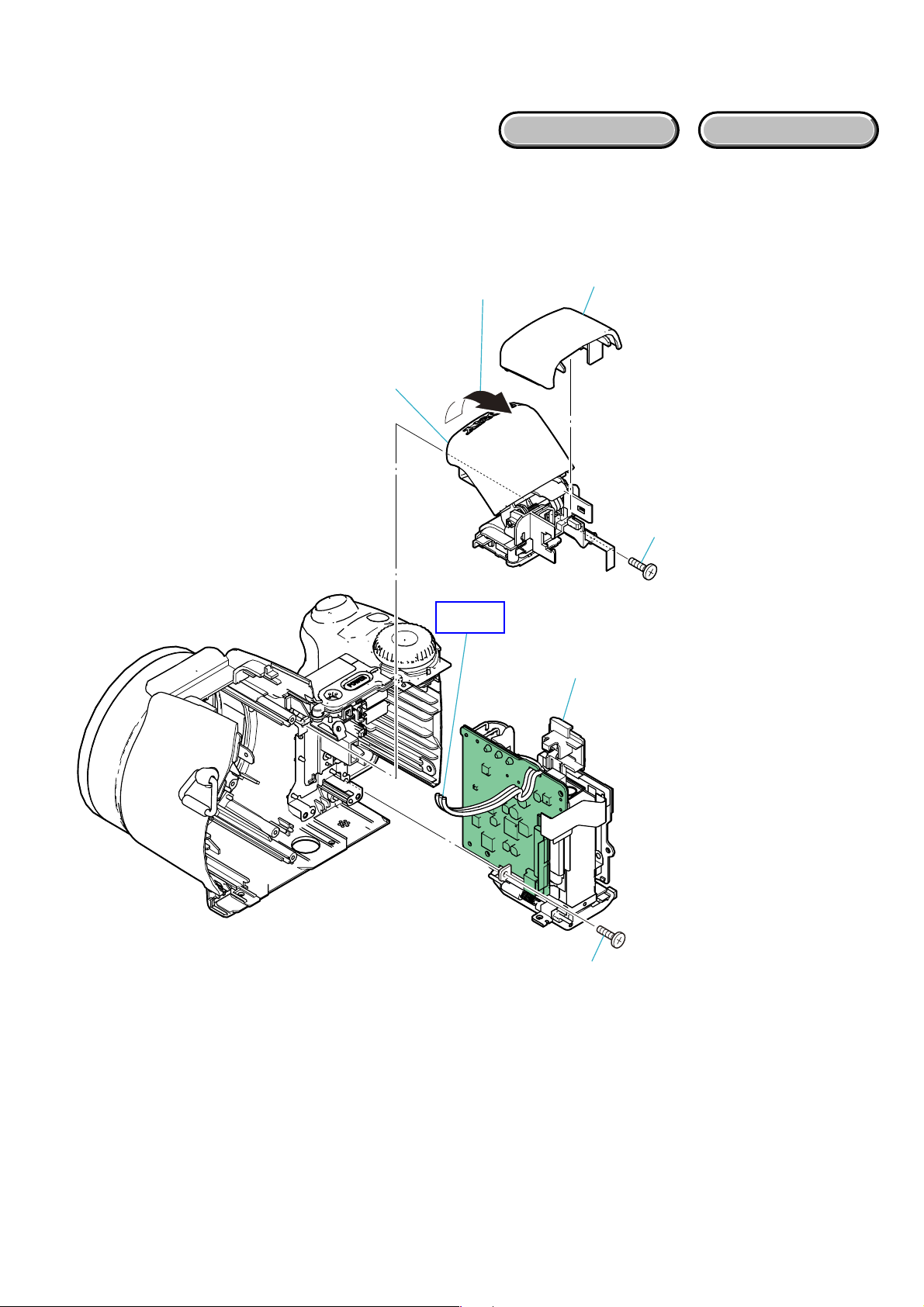
Assembling procedures that require attention are described here.
When installing theree harness, do not intersect the harness in the part between “a” and “b” as shown in figure.
b
a
Strobe harness
Strobe harness
Arrange the strobe harness
in this range.
Rib
Arrange the strobe harness
inside of the rib
Rib
DSC-H7/H9_L2
HELP
Page 23

CK-182 flexible board arrangement
Blind Assy, Cabinet (Rear)
Panel Block Assy
CK-182 flexible board sticking
CK-182 board
adhesive sheet (4.5mm x 12mm)
(Note)
Cabinet (C) Assy (B), (P)
CK-182 board
25mm
Note: 接着紙(2-649-300-01)を切って使用。
Note : Cut SHEET, ADHESIVE (2-649-300-01)
DSC-H7/H9_L2
into the desired length and use it.
HELP
Page 24

On assembling, set the NS lever and the NIGHTSHOT switch up and adjust the notch of NS upper arm to the projection on NS lever.
NS lever
Upper arm, NS
NIGHT SHOT
switch
Cabinet (Rear) Block Assy
When assembling the mode dial, match the direction of the cutting lack as shown in figure
Cutting lack
DSC-H7/H9_L2
HELP
Page 25

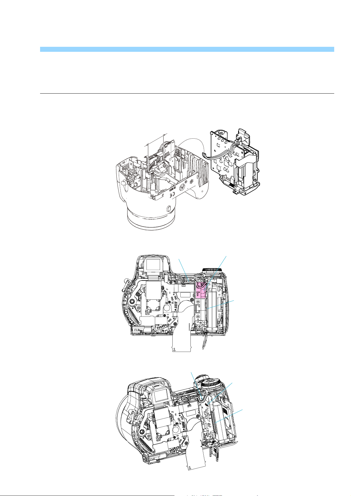
3. BLOCK DIAGRAMS
Link
Link
OVERALL BLOCK DIAGRAM (1/2) POWER BLOCK DIAGRAM (1/2)
OVERALL BLOCK DIAGRAM (2/2)
POWER BLOCK DIAGRAM (2/2)
DSCH7/H9_L2
Page 26

3. BLOCK DIAGRAMS
3-1. OVERALL BLOCK DIAGRAM (1/2) ( ) : Number in parenthesis ( ) indicates the division number of schematic diagram where the component is located.
LENS
SE501
PITCH
SENSOR
SE502
YAW
SENSOR
FILTER
LENS UNIT
IR
ACTIVE LENS ACTUATOR
IRIS/
SHUTTER
MOTOR
SHUTTER
MOTOR
FOUCS
MOTOR
MOTOR
(IR FILTER IN)
FOCUS RESET
SENSOR
ZOOM RESET
SENSOR
ZOOM DC FG
PITCH
ZOOM
H
YAW
H
LPFBIN2
4
1
4
1
1
5
21
18
VREFB
LPFAIN2
VREFA
IRIS
M
M
M
M
IC506
PITCH/YAW
SENSOR
AMP
(7/7)
CD-703 FLEXIBLE BOARD
17
IC003
15, 1631, 323 - 14
CCD
IMAGER
26, 27, 28, 29
19
30
1
24
23
CN401
IRIS_A/B
IRIS_XA/XB
F2, E2, D2, B1
SHUTTER+/–
1 - 819 - 2258 - 6141, 42, 44, 4535, 3736, 3847, 48, 50, 5131, 33 30, 32 54, 55 12 - 15
FOCUS_A/B
FOCUS_XA/XB
D6, E6, B7, C6 F3, F4B4, B5
ZOOM+/–
28
27
FC_PI_Anode
25
17
ZM_PI_Anode_1st
18
56
LENS_TEMP
24
TZ_HALL_TEMP
34
PITCH +/–
PITCH HALL+/–
PITCH_HALLBIAS+/–
YAW+/–
YAW HALL+/–
YAW_HALLBIAS–
CLK
PITCH AD
10
YAW AD
13
24
25
SWBOUT
SWAOUT
DATA
IC004
10 14
CCD IMAGE SENSOR
OUTPUT
1, 16
BUFFER
SUB_CONT
IC401
(1/2)
(1/7)
IRIS DRIVE
SHUTTER DRIVE
FOCUS MOTOR
DRIVE
ZOOM MOTOR
DRIVE
Q401 (1/2)
LED DRIVE
Q401 (2/2)
LED DRIVE
B1, D1H2, J4J2, J3J7, J9G6, J8 B10, D10
STEADY SHOT
CH1
G5
J5
CH3
D5
CPU_PIO_0
D6
CPU_PIO_1
F5, E5, D3, F1
D5, A6, B6, C5 G1, E4A2, B2G3, G4
IC503
CONTROL
(7/7)
SY-177 BOARD (1/2)
CN301
CCD_OUT
44
PS
1
VST1, VST2
VLHD1, VLHD2
LH1, H1, H2, H3
36, 30, 32, 34 8, 93, 45 - 7, 10 - 18
RG
38
V1, V2, V3A, V3B, V4,
V5A, V5B, V6 - V10
LV
2
SUB
CSUB
SUB
24
23
22
Q302
IRIS_DIR_A/B
IRIS_BRK_A/B
MSHUT_DIR, MSHUT_EN
FC_DIR_A/B, FC_EN
ZM_DIR_A, ZM_BRK_A
MSHUT_DIR
Q403, 404
IR FILTER_IN
FC SENS
XFC_RST_LED
ZM_SENS_1ST
XZM_RST_LED
ZM_DC_FG_1A, ZM_DC_FG_1B
XEM_FG_LEDXEM_FG_LED
LENS_TEMP
TZ_HALL_TEMP
CA_FD
C9
IC_211_0_SO
A4
IC_211_0_SI
B4
XIC_211_0_SCK
B5
XCS_IC_503
A5
CLK_IC_503
A3
XIC_211_IC_503_RST
A6
XDD_SYS_RST
A7
OVERALL
(2/2)
X201
36MHz
CCDIN
L7
CA_AD0 - CA_AD13
J8
IC301
C5, B5E6, E7
L2, K1, K2,
L4
G9, F9, J9,
C8
G7
Q301
F11
VSUB_CONT_PRE
VSUB_CONT_POST
XDD_SYS_RST XDD_SYS_RST
4
(2/7)
A/D CONV. S/H,
TIMING
GENERATOR
D1, D2
H1, H2,
F6, F7, G5,
E9, D9, F5,
C4, E5, D10
IC_211_0_SO
IC_211_0_SI
XIC_211_0_SCK
GEAR_ONICLK
TG_OUT
SYS_OUT
IC202
CLOCK GENERATOR
(4/7)
A4, A3
C7, A8, A7, B7,
B6, A6, A5, B4,
B10, B8, B9, C6,
CA_HD
HD
E10
CA_FD
D11
VD
GEN_TG_CLK
J5
XCS_FE
K9
IC_211_3_SO
K10
XIC_211_3_SCK
L10
XDD_SYS_RST
E11
OVERALL
3
(2/2)
GEAR_ON
32
GEN_TG_CLK
1
GEN_SYS_CLK
5
AF19, AE18
AE20, AF20, AE19,
AC18, AE21, AF21,
AB21, AC21, AB20,
AC20, AB19, AC19,
AE23
AF22
AF18
V19
C25
D19
R7
AF25
D9
Y10
M8
AD26
J8
AE3
AF3
L8
H17
A24
G17
U8 H8
W13
H10
Y13
Y12
CAMERA
SYSTEM CONTROL
W16, Y18
AD25, Y17
R8, AE25
W17
W18, AB26,
AB23, AA23Y11, W11
IC211
(1/2)
DSP/
(3/7)
(4/7)
(5/7)
A19, E16, A18,
D17, B19, E17,
A15, B13, B14,
D16, A17
LCD_HD, LCD_VD, LCD_CK
D18, B17, B18E18, B23
XIC_211_2_SCK
U19
OVERALL
1
OVERALL
(2/2)
U7
A13, B15, A14
LCD_D0 - LCD_D7 D0-D7
IC_211_2_SO
XCS_PANEL
2
BL_H
BL_L
(2/2)
IC_211_2_SO
XIC_211_2_SCK
XCS_EVF
CN709
16, 18, 20, 22, 24, 26, 28, 308, 12, 1413, 1529, 27
11
7
LCD_D0 - LCD_D7
CN703
9 -11, 13 - 16
17, 19 4 - 6
20
3
CN706
5, 7, 9, 11, 13,15
1
11
7
11
7
HSYNC,
VSYNC,
CLOCK
SDAT, SCLK
XCS_EVF
NRESET
MS-365 FLEXIBLE
BOARD
MSX_D0 - MSX_D3,
SCLK, MSX_BS
XACCESS_LED
BOARD
16, 18, 20, 22, 24, 26, 28, 308, 12, 1413, 1529, 27
HD, VD, LCD_CK HD, VD, DCK
IC_211_2_SO
XIC_211_2_SCK
XCS_PANEL
XDD_SYS_RST
BL_H, BL_L
CN001 CN002
BOARD
16, 18, 20, 22, 24, 26, 28, 308, 12, 1413, 1529, 27
HD, VD, LCD_CK
IC_211_2_SO, IC_211_2_SCK
XCS_PANEL
XDD_SYS_RST
BL_H, BL_L
CN001 CN002
LCD903
EVF UNIT
CK-179 BOARDCK-182 FLEXIBLE
16 - 2315, 14,127, 828, 27
6
4
CK-180 BOARDCK-181 FLEXIBLE
16 - 2315, 14, 127, 828, 27
6
4
MS-366 BOARD
CN301
5, 7, 9, 11, 13,15
1
D301
(ACCESS)
MS-364 BOARD
CN301
5, 7, 9, 11, 13,15
1
D301
(ACCESS)
CN001
SI, SCK
XCS
RESET
CN001
D0-D7
HSYNC, VSYNC, DCLK
SPDA, SPCK
SPENA
RESET Z
DSC-H9
6 - 1314 - 1618, 171, 2
LCD901
3INCH
LCD UNIT
With
BACK LIGHT
19
20
DSC-H7
3 - 1011 - 1335, 34
LCD902
2.5INCH
LCD UNIT
36
37
LCD9001
BACK
LIGHT
A : VIDEO SIGNAL
A : AUDIO SIGNAL
A : VIDEO/AUDIO SIGNAL
DSC-H9
CN302
MEMORY
STICK Duo
CONNECTOR
DSC-H7
CN302
MEMORY
STICK Duo
CONNECTOR
DSC-H7/H9_L2
3-1
Page 27

3-2. OVERALL BLOCK DIAGRAM (2/2) ( ) : Number in parenthesis ( ) indicates the division number of schematic diagram where the component is located.
DSC-H9
CONTROL SWITCH BLOCK
(SW60350)
S001 - S005
KEY_AD1
S106
JOG
SWITCH
PY-002 FLEXIBLE
BOARD
S002
FINDER/LCD
S001
JOG_A/B
CN104
B
DSC-H9
PL-047 BOARD
CN201
RY201
(PLUNGER)
3, 4
S201
(STRB-POPUP)
2
DSC-H7
PL-046 BOARD
RY201
CN201
(PLUNGER)
3, 4
S201
(STRB-POPUP)
2
A : VIDEO SIGNAL
A : AUDIO SIGNAL
A : VIDEO/AUDIO SIGNAL
3
1, 6
SW-499 BOARD SY-177 BOARD (2/2)
CN102
3
1, 6
S101 - S104
ZOOM T ZOOM W
6
5
MENU HOME
CN103
KEY_AD1
JOG_A/B
KEY_ZOOM
DIRECT_PB
CN101
DSC-H7
SW504 FLEXIBLE
BOARD
5
1, 2
6
8
CN701
4
8, 7
3
1
SW-500 BOARD
CN102
3
1, 6
6
5
CN103
S101 - S104
ZOOM T ZOOM W
MENU HOME
S101 - S104
CN101
JOG_A/B
KEY_ZOOM
DIRECT_PB
5
1, 2
6
8
FLEXIBLE FLAT CABLE (PL-002)
3, 4
2
STRB_PLUNGER
XSTRB_POPUP
CN704
3, 4
5
PW-134 FLEXIBLE BOARD
CN702
17
2
11
14
5, 3 8, 9
6
15
IC001
REMOTE
CONTROL
RECIEVER
DSC-H9
AF ILLUMINATOR/
( )
SELF-TIMER
S006
(SHUTTER)
S001
(POWER)
S005
12 POSITION
MODE_DASL
S003, S004
/ BRK
z
D001
(NIGHT SHOT)
D002
D003
(POWER)
XAF_LED
XPWR_LED
XAE_LOOK
XSHUT_SW
XPWR_SW
SIRCS_SIG
KEY_AD2
XNS_LED
IC401
(2/2)
ZOOM/FOCUS/
IRIS/
SHUTTER
DRIVE
(1/7)
B3 A1
Q702, 703
CURRENT
CONTROL
Q707
LED
DRIVE
IC201
BATT-SIG
I/F
(3/7)
KEY_ZOOM
XLENS_DRIVER_PS
D4
STRB_PLUNGER_ON
XSTRB_POPUP_SENS
MODE_DIAL1/2
IC_211_1_SO,
IC_211_1_SI,
IC_211_1_SCK
C5, D5, B5
XCS_IC_201
B1
E4
B2
KEY_AD1
JOG_A/B
KEY_AD2
AC8
G16, H16
AC7
H11
B21
A21
G15
Y9
R19, N19AB7, AE6
G10
AF6
N8
B24, G18, H18
W20
IC211
(2/2)
CAMERA
DSP/
SYSTEM
CONTROL
(3/7)
(4/7)
(5/7)
AF8
AE8
V8
IC_211_CVOUT
AB13
VOUT_1
AF12
VOUT_2
AC12
XHD_EN
V7
G9
Y1, AA1
G19, D26
H9
V2
H15
Y16
OVERALL
G8
A23
W7
OVERALL
AB18
IC_211_AUIN
IC_211_AUOUT
XCS_AUDIO
1
OVERALL
(1/2)
3
(1/2)
2
OVERALL
(1/2)
4
(1/2)
A6
B6
D6
F3
Q241 - 244
BUFFER
IC_211_2_SO
IC_211_2_SCK
IC_211_0_SO
IC_211_0_SI
IC_211_0_SCK
BL_H
BL_L
XDD_SYS_RST
IC602
VIDEO/AUDIO
AMP
(6/7)
D5, E6
FLEXIBLE
BOARD
2
1
4
3
17
16
15
8
7
27 - 30
11
10
9
A1, C1
A3
E2
MUTE
E1
F1
IC_211_1_UO, IC_211_1_UI
DD-272 BOARDDD-273
CN302CN708
XSTRB_FULL
2
STRB_CHG
1
STRB_CHG_CONT
4
STRB_ON
3
IC_211_0_SO
17
IC_211_0_SI
16
IC_211_0_SCK
15
XPWR_OFF
8
XCS_FR
7
31 - 34
1313
1818
BATT_SIG
11
DIRECT_PB
10
XPWR_ON
9
CN705
SP+/–
CN710
MIC_SIG
AU_LINE_OUT
V_LINE_OUT
IC_211_YOUT
IC_211_PBOUT
IC_211_PROUT
XAV_JACK_IN
USB_DP/DM
BL_H, BL_L
GPS_13
Q202, 203
IC103
RESET
(2/3)
14
OUT VDD
CN707
D1
D2
E1
B9
E2
B4
1, 2
2
12
14
16
4
2
B7 B8
18
IC101
SYSTEM
CONTROL
LF001
7, 9
IC201
FLASH/
(3/3)
F002
UART_TX, UART_RX
1, 2
ONSU
J8
ONM
E9
ONAFE
E8
ONSD
D9
ONINV
B2
19, 20
ST_UNREG
9
10
CHARGE
6
CONTROL
47
(2/3)
F001
Q013
SP901
SPEAKER
MIC901
MIC UNIT
AU_OUT_L
V_OUT
HD_Y
HD_PB
HD_PR
XAV_JACK_IN
USB_DP/DM
T201
46
3
10
15
1, 22
CONVERTER
LF002
Q201
IC001
IC002
IC003
IC007
IC102
DC/DC
IC006
D002Q004
CN301
16
20
24
4
2
26
9, 15 10, 12
D202
C205
(1/3)
(1/3)
(1/3)
(1/3)
(2/3)
(1/3)
1 - 47 - 10
6
+
S
–
CN001
MULTI
( )
CONNECTOR
ST-166
FLEXIBLE BOARD
TI_5V
CAM_12V
CAM_–7.5V
D_3.0V
A_3.0V
D_1.8V
D_3.0V (MS_VCC)
DDR_1.8V
D_1.2V
MAX_5.0V
PANEL_6.4V
DD-107
FLEXIBLE
BOARD
BH001
BATTERY
( )
TERMINAL
DSC-H9
FL901
FLASH
UNIT
J001
DC-IN
DSC-H7/H9_L2
3-2
Page 28

3-3. POWER BLOCK DIAGRAM (1/2) ( ) : Number in parenthesis ( ) indicates the division number of schematic diagram where the component is located.
CN001
MULTI
( )
CONNECTOR
J001
DC IN
JK-338 FLEXIBLE BOARD
ACV_UNREG
23, 25
ACV_GND
BATT/XEXT
USB_VBUS
BATT_XEXT
6
+
S
–
6
19
ACV_UNREG
DC-107
FLEXIBLE
BOARD
BH001
BATTERY
( )
TERMINAL
CN301
1 - 47 - 10
D003
XACV_IN
BATT_SIG
Q101(1/2)
32.768kHz
XMS_IN
X101
Q101(2/2)
LF002
D002
(1/2)
CN707
22 - 25
5
21
D8
J4
J5
C6
ACV_UNREG2
USB_VBUS
BATT/XEXT
SYSTEM CONTROL
XUSB_JACK
32kHz_IN
32kHz_OUT
MS_IN
DD-273 FLEXIBLE BOARD
(1/2)
CN708
(1/2)
55 - 58
5
26
Q004
IC101
(2/3)
DDC1P8_RESET
DDC2P9_AD
DDC1P8_AD
BACK_UP_VCC
BACK_UP_VCC
DDC2P9_EN
DDC1P8_EN
DDC1P2_EN
CAMDD_EN
LDO1P8_EN
DISW1P8_EN
DISW2P9_EN
DDC5PSW_EN
XPOWER_OFF
XRESET_REQ
XPOWER_ON0
XPOWER_ON2
AVCC
XSYS_RST
VSU_EN
PANEL_EN
EVER_PSB
DDCPV_EN
SW1P8_EN
BL_EN1
BL_EN2
XRSTX
FR_SI
FR_SO
FR_SCK
XCS_EX
C8
H7
J7
A5
H9
H4
B4
J8
E9
E8
D9
B2
B1
J9
C9
J1
H2
C2
C1
F7
F8
F9
D7
B9
A1
B8
B7
D1
D2
E1
E2
Q013
PANEL_EN
EVER_PSB
DDCPV_EN
SW_1P8_EN
LDO_1P8_EN
DISW1P8_EN
DISW2P9_EN
DDC5PSW_EN
BL_EN1
BL_EN2
XRSTX
XPWR_OFF
XIC_211_RST_REQ
XPWR_ON
DIRECT_PB
IC_211_0_SO
IC_211_0_SI
XIC_211_SCK
XCS_FR
DD-272 BOARDSY-177 BOARD
CN302
(1/2)
59 - 62
5
30
ACV_UNREG
IC007
+1.2V REG.
(1/3)
VOUT
1
D_3.0V
D_1.8V
ACV_UNREG2
VIN
4
DC/DC CONVERTER
ONSU
46
ONM
3
ONAFE
10
ONSD
15
ONINV
1
ONBST
22
IC001
(1/3)
F001
F002
ST_UNREG
PVM
BATT
PVINV
FBINV
LXINV
LXM
FBM
PVAFE
LXAFE
FBAFE
PVSD
LXSD
FBSD
PVBST
SWBST
LXBST
FBBST
PVSU
LXSU
FBSU
SWLED
LXLED
FBHLED
FBLLED
PVLED
ONLED
EVER_3.0V
STRB_ON
T201
D202
C205
Q201
PANEL_6.4V
XSTRB_FULL
STRB_CHG
STRB_CHG_CONT
STRB_ON
GPS_13
XDD_SYS_RST
CAM_12V
CAM_–7.5V
D_3.0V
A_3.0V
D_1.8V
D_3V (MS_VCC)
DDR_1.8V
D_1.2V
MAX_5.0V
XMS_IN
XPWR_OFF
XIC_211_RST_REQ
XPWR_ON
DIRECT_PB
IC_211_0_SO
IC_211_0_SI
XIC_211_SCK
XCS_FR
XACV_IN
BATT_SIG
CN302
TI_5V
BL_H
BL_L
(2/2)
Q202, 203
DSC-H9
6
1
SW
EN
VBAT
LBI
VDD
4
VIN
4
CE
1
+1.8V REG.
IC006
+6.5V REG.
(1/3)
VIN
VCONT
IC002
+5V REG.
(1/3)
IC103
RESET
(2/3)
L001
VOUT
IC003
(1/3)
OUT
VOUT
VOUT
PS
1
3
GPS_13
L002
Q014
Q003
Q006
D009
9
1
6
7
D008
PANEL_EN
EVER_PSB
4
DDCPV_EN
45
20
25
21
5
2
9
8
11
13
16
12
GD
28
29
30
31
26
44
SU
43
47
42
34
33
38
37
35
36
D010
L008
L005
L006
L009
D011
L004
L007
L003
BL_EN1 BL_EN2
XRSTX
SW_1P8_EN
LDO_1P8_EN
Q007
DISCHARGE
DISW1P8_EN
DISW2P9_EN
D007
DDC5PSW_EN
D006
4
2
8
TI_5V
D102
BH101
LITHIUM
BATTERY
L201
D101
Q010, 012
VIN
7
CS
4
XRESET
5
VCH
2
VBAT
3
D_3.0V
A_3.0V
D_1.8V
D_1.2V
CAM_12V
MAX_5.0V
IC201
FLASH/CHARGE
CONTROL
(3/3)
G_IGBT
XFULL
I_PEAK
VCC
VOUT
6
VRO
8
SWVBATT
SW
CHG
F_ON
IC102
BATTERY
CHECK
(2/3)
115
2
7
9
10
6
43
XSTRB_FULL
STRB_CHG
STRB_CHG_CONT
D203
ST-166
FLEXIBLE
BOARD
FL901
FLASH
UNIT
65
40, 4142 - 4445 - 4736 - 39 48, 4963, 6450, 5131, 3233, 34 57, 58
2
1
4
3
13
18
53
54
61
36, 3738 - 4041 - 4332 - 35 44, 4559, 6046, 4727, 2829, 30 53, 54
2
1
4
3
13
18
49
50
5
TO
POWER
(2/2)
66
8
7
9
10
17
16
15
14
12
11
FLEXIBLE
DD-273
BOARD
8
7
9
10
17
16
15
14
12
11
(2/2)
DSC-H7/H9_L2
3-3
Page 29

5
TO
POWER
(1/2)
3-3. POWER BLOCK DIAGRAM (2/2) ( ) : Number in parenthesis ( ) indicates the division number of schematic diagram where the component is located.
SY-177 BOARD (2/2)
CN708
(2/2)
BL_H
27, 28
BL_L
29, 3036, 3738 - 4053, 5444, 4559, 6046, 4741 - 4332 - 35
PANEL_6.4V
61
TI_5.0V
XSTRB_FULL
2
STRB_CHG
1
STRB_CHG_CONT
4
STRB_ON
3
GPS_13
13
XDD_SYS_RST
18
CAM_12V
49
CAM_–7.5V
50
D_3.0V
A_3.0V
D_1.8V
D_3.0V (MS_VCC)
DDR_1.8V
D_1.2V
MAX_5.0V
XMS_IN
6
XPWR_OFF
8
XIC_211_RST_REQ
7
XPWR_ON
9
DIRECT_PB
10
IC_211_0_SO
17
IC_211_0_SI
16
XIC_211_0_SCK
15
XCS_FR
14
XACV_IN
12
BATT_SIG
11
STRB_CHG
STRB_ON
STRB_CHG_CONT
GPS_13
XSTRB_FULL
XFC_RST_LED
XZM_RST_LED
AB18
XRESET
V2
USB_VBS_EN
Y16
STRB_ON1
H15
TPU3_OUT
W7
GPS_13
G8
GPE_00
W12
XRESET_REQ
H17
SIO0_TXD
A24
SIO0_RXD
G17
SIO0_SCK
A23
SIO0_SCS
K8
GPE_05
GPE_07
H9
GPE_04
M8
GPE_03
J8
IC304
+3.5V REG.
(2/7)
VOUTVIN
FB281
34
1
CE
FB283
R254
D_1.8V_DDR
CAMERA DSP,
SYSTEM CONTROL
FB282
IC211
(3/7)
(4/7)
(5/7)
CAM_3.5V
CAM_3.5V
R253
R829
TPU2_OUT
XDD_SYS_RST
L211
GPS_11
GPE_15
CN709
PANEL_6.4V
D_3.0V
BL_H
BL_L
L241
V7
T7
G15
3
1
29
27
7
VIDEO
BUFFER
Q242 - 244
L242
Q241
BOARD
CN001
PANEL_6.4V
3
D_3.0V
1
BL_H
29
BL_L
27
XDD_SYS_RST
7
AU_AVCC
D_3.0V
MAX_5.0V
D_1.8V
D_3.0V
MXA_5.0V
D_3.0V
A_3.0V
2
1
28
27
4
B2
1
4
IC506
PITCH/YAW
SENSOR AMP
(7/7)
R602
L602
IC602
VIDEO/AUDIO
AMP
(6/7)
CK-179 BOARDCK-182 FLEXIBLE
CN002
P_6.4V
D_3V
BL_H
BL_L
XDD_SYS_RST
IC305
+2.3V REG.
(2/7)
VOUTVIN
IC502
+1.5V REG
(7/7)
VOUTVIN
IC501
+2.8V REG.
(7/7)
CE
VOUT
VDD
R606
34
B1
3
L601
L002
VCC2 (6.4V)
L001
7A B2
IC503
STEADY SHOT
RESET_N
CONTROL
(7/7)
IC401
ZOOM/FOCUS/IRIS/
SHUTTER DRIVE
(1/7)
CN001
VCC1
VCC (3V)
BL_H
BL_L
BL_L
RESET
RGVDD
CAM_–7.5V
IC306
+1.8V REG.
(2/7)
D_3.0V
HVDDH1/H2/H3
MAX_5.0V
D_1.8V
A_3.0V
SE501, 502
PITCH/YAW
SENSOR
37
36
38
1
2
3
20
VOUTVIN
E11
FE_1.8V
B1B2
FB303
FB306
FB305
RSTB
TIMING GENERATOR
BATT-SIG
XRESET
TXRX
E4
BATT_SIG
D_3.0V
MS_PWR_ON
MAX_5.0V
XFC_RST_LED
D_3.0V
XZM_RST_LED
LCD901
3INCH
LCD UNIT
With
BACK LIGHT
IC303
+13V REG
(2/7)
VOUTVIN
FB302
IC301
A/D CONV, S/H
(2/7)
IC201
I/F
(3/7)
45
CLOCK
GENERATOR
IC202
(4/7)
CN001
D_3.0V D_3.0V
1
BL_H
29
BL_L
27
XDD_SYS_RST
7
Q303
DISCHARGE
FB301
Q702, 703
Q401
BOARD
L301
L302
IC701
+2.5V REG.
(4/7)
VOUTVDD
L702
ZM_PI_ANODE_1st
CK-180 BOARDCK-181 FLEXIBLE
CN002
1
BL_H
28
BL_L
27
4
CN301
CAM_12VCAM_12V
CAM_–7.5V
CN703
2.5V
34
5.0V
CN701
A_3.0V
DIRECT_PB
CN706
MS_VCC
XMS_IN
MS_PWR_ON
CN702
R718,
R719
XPWR_ON
CN401
FC_PI_ANODE
ZM_FG_PI_VCC
CN001
PVDD
18
VDD
L002
VDDREG
RESET Z
BL_H
32
38
37
BL_L
CD-703 FLEXIBLE BOARD
IC004
40
20
1
12
22
3
CCD IMAGE
SENSOR
OUTPUT BUFFER
LCD902
EVF
UNIT
SW-499 BOARD
CN101 CN102
A_3.0V
6
1
3
8
DIRECT_PB
SW-500 BOARD
CN101 CN102
A_3.0V
SW-504
FLEXIBLE
BOARD
3
8
DIRECT_PB
MS-366 BOARD
Q301
2
44
3
2
3
CN301
MS-364 BOARD
Q301
2
4
MS-365
FLEXIBLE
BOARD
PW-134 FLEXIBLE
BOARD
D_3.0V
13
D_3.0V
1
AF_5V
18
NS_VCC
16
11
25
18
53, 57
3
D003
(POWER)
(NIGHT SHOT)
FC SENSOR
ZOOM SENSOR
ZOOM FC
CN301
D001
IC001
REMOTE
CONTROL
RECEIVER
( )
LENS
UNIT
DSC-H7DSC-H9
LCD901
2.5INCH
LCD UNIT
LCD9001
BACK
LIGHT
IC003
CCD
IMAGER
DSC-H9
2
CN103
5
DSC-H7
2
CN103
5
9
FB305
6
D301
(ACCESS)
9
FB305
6
D301
(ACCESS)
D002
AF ILLUMINATOR/
SELF-TIMER
S001
(POWER)
CONTROL SWITCH
(SW60350)
PY-002
FLEXIBLE
BOARD
DSC-H9
CN302
MEMORY
STICK Duo
CONNECTOR
CN302
MEMORY
STICK Duo
CONNECTOR
DSC-H7
BLOCK
S001
B
DSC-H7/H9_L2
3-4E
Page 30

4-1. FRAME SCHEMATIC DIAGRAM
4. PRINTED WIRING BOARDS AND SCHEMATIC DIAGRAMS
DSC-H7
MS-364 BOARD (SIDE A
1
MEMORY STICK DUO
10
MS-364 BOARD (SIDE B
16
1
CN301
DSC-H7
SW-500 BOARD (SIDE A
16
CN102
SW-500 BOARD (SIDE B
CN103
1
6
DSC-H9
SW-499 BOARD (SIDE A
16
CN102
SW-499 BOARD (SIDE B
CN302
CONNECTOR
DSC-H9
DD-273 FLEXIBLE BOARD
)
11
LOCKLOCK
12
)
MS-366 BOARD (SIDE A
1
MEMORY STICK DUO
10
MS-366 BOARD (SIDE B
116
CN301
)
11
CN302
CONNECTOR
12
)
1
61
PW-134 FLEXIBLE BOARD
1
18
1
LEVEL3
DD-272 BOARD
65
65
64
ST-166
FLEXIBLE BOARD
LND203
LND202
LND201
C205
CHARGING
CAPACITOR
FL901
FLASH
UNIT
LND006
LND004
LND005
DC-107
FLEXIBLE BOARD
J001
DC IN
LND003
10
WHITE
BLUE
LND002
PINK
LND001
1
(SIDE A)
1
2
CN302
3
1
2
BH101
BT001
LITHIUM BATTERY
BH001
BATTERY
TERMINAL
-
S
+
MS-365 FLEXIBLE BOARD
PY-002 FLEXIBLE BOARD
1
6
)
MIC901
18
SW-504 FLEXIBLE BOARD
)
CN101
18
1
8
CD-703 FLEXIBLE BOARD
1
IC003
(Not supplied)
1215
CN706
118
CN702
IC211
(Not supplied)
12
CN710
29
30
CN709
1
2
LEVEL3
SY-177 BOARD
(SIDE A)
CN708
127
44
45
8
1
260
1225
21
CN705
61
CN401
260
1
24
CN707
LENS UNIT
SP901
LEVEL3
SY-177 BOARD
(SIDE B)
CN703
122
61
16
CN701
2
CN301
1
PL-046 BOARD
(
)
SIDE A
16
CN201
16
CN704
FLEXIBLE FLAT CABLE (PL-002)
LCD9003
COLOR
EVF UNIT
CK-181 FLEXIBLE BOARD
29
30
CN001
1
2
)
DSC-H7
45
125
JK-338 FLEXIBLE BOARD
CONTROL SWITCH
BLOCK
)
(SW60350)
DSC-H9
PL-047 BOARD
(
)
SIDE A
16
CN201
DSC-H7
DSC-H9
LCD902
2.5 inch
COLOR
LCD UNIT
1
28
LCD901
3.0 inch
COLOR
LCD UNIT
CN301
10
9
1
2
CK-180 BOARD
(
)
SIDE A
LND005
LND004
CK-179 BOARD
(
SIDE A
LEVEL3
DD-272 BOARD
(SIDE B)
12
CN002
8
2
CN001
1
)
38
39
CN002
21
8
DSC-H7/H9_L2
CN103
6
CN101
18
1
CN001
MULTI CONNECTOR
226
2728
125
CK-182 FLEXIBLE BOARD
30
29
CN001
1
2
1
28
4-1
2
40 41
CN001
1
38
39
LND001
FRAME
Page 31

Link
Link
4-2. SCHEMATIC DIAGRAMS
CD-703 FLEXIBLE BOARD (CCD IMAGER)
CK-180 BOARD:DSC-H7
(SY TO LCD RELAY)
CK-181 FLEXIBLE BOARD:DSC-H7
(SY TO CK RELAY)
CK-179 BOARD:DSC-H9
(SY TO LCD RELAY)
CK-182 FLEXIBLE BOARD:DSC-H9
(SY TO CK RELAY)
JK-338 FLEXIBLE BOARD
MS-364 BOARD:DSC-H7
(MS CONNECTOR)
MS-365 FLEXIBLE BOARD
MS-366 BOARD:DSC-H9
(MS CONNECTOR)
PY-002 FLEXIBLE BOARD (SWITCH)
(MULTI CONNECTOR)
(SY TO MS RELAY)
SW-499 BOARD:DSC-H9
(SWITCH)
SW-500 BOARD:DSC-H7
(SWITCH)
SW-504 FLEXIBLE BOARD
PL-046 BOARD:DSC-H7
(PLUNGER)
PL-047 BOARD:DSC-H9
(PLUNGER)
PW-134 FLEXIBLE BOARD
DC-107 FLEXIBLE BOARD (DC IN)
DD-273 FLEXIBLE BOARD
ST-166 FLEXIBLE BOARD (FLASH UNIT)
(SY TO SW RELAY)
(FUNCTION SWITCH)
(SY TO DD RELAY)
DSC-H7/H9_L2
COMMON NOTE FOR SCHEMATIC DIAGRAMS
Page 32

4-2. SCHEMATIC DIAGRAMS
4-2. SCHEMATIC DIAGRAMS
4-2. SCHEMATIC DIAGRAMS
THIS NOTE IS COMMON FOR SCHEMATIC DIAGRAMS
(In addition to this, the necessary note is printed in each block)
(For schematic diagrams)
• All capacitors are in µF unless otherwise noted. pF : µ
µF. 50 V or less are not indicated except for electrolytics
and tantalums.
• Chip resistors are 1/10 W unless otherwise noted.
kΩ=1000 Ω, MΩ=1000 kΩ.
• Caution when replacing chip parts.
New parts must be attached after removal of chip.
Be careful not to heat the minus side of tantalum
capacitor, Because it is damaged by the heat.
• Some chip part will be indicated as follows.
Example C541 L452
22U 10UH
TA A 2520
Kinds of capacitor
External dimensions (mm)
Case size
• Constants of resistors, capacitors, ICs and etc with XX
indicate that they are not used.
In such cases, the unused circuits may be indicated.
• Parts with ★ differ according to the model/destination.
Refer to the mount table for each function.
• All variable and adjustable resistors have characteristic
curve B, unless otherwise noted.
• Signal name
XEDIT→ EDIT PB/XREC → PB/REC
• 2: non flammable resistor
• 5: fusible resistor
• C: panel designation
• A: B+ Line
• B: B– Line
• J : IN/OUT direction of (+,–) B LINE.
• C: adjustment for repair.
• A: not use circuit
(Measuring conditions voltage and waveform)
•Voltages are measured between the measurement
points and ground when camera shoots color bar chart
of pattern box. They are reference values and reference
waveforms.
(VOM of DC 10 MΩ input impedance is used)
•Voltage values change depending upon input
impedance of VOM used.)
1. Connection
Pattern box
Pattern box PTB-450
J-6082-200-A
or
Small pattern box
PTB-1450
J-6082-557-A
L = About 30 cm (PTB-450)
L = About 13 cm (PTB-1450)
Pattern box
Color bar chart
L
For PTB-450:
J-6020-250-A
For PTB-1450:
J-6082-559-A
Front of the lens
Camera
2. Adjust the distance so that the output waveform of
Fig. a and the Fig. b can be obtain.
H
Yellow
Cyan
White
Magenta
Green
AABBA=B
Fig. a (Video output terminal output waveform)
Fig.b (Picture on monitor TV)
Red
Blue
Electronic beam
scanning frame
CRT picture frame
Precautions for Replacement of Imager
• If the imager has been replaced, carry out all the adjustments
for the camera section.
• As the imager may be damaged by static electricity from
its structure, handle it carefully like for the MOS IC.
In addition, ensure that the receiver is not covered with
dusts nor exposed to strong light.
DSC-H7/H9_L2
When indicating parts by reference number, please
include the board name.
The components identified by mark 0 or dotted line with
mark 0 are critical for safety.
Replace only with part number specified.
Les composants identifiés par une marque 0 sont
critiques pour la sécurité.
Ne les remplacer que par une pièce portant le numéro
spécifie.
4-2
Page 33

1 5 11476109832
Note: Voltages of IC003 and IC004 can not be
CD-703 FLEXIBLE BOARD
A
CCD IMAGER
Note: CD-703 FLEXIBLE BOARD is not supplied.
But this is included in CCD BLOCK ASSY.
measured, because they are mounted on
the side of the lens.
VST1
VST2
V10
V9V8V7
V6
V5B
V5AV4V3B
V3A
V2
V1
B
C
D
E
G
H
6
7V48
V3B
V5A
V5B
9
V6
10
V7
11
LND001
LND002
LND003
LND004
LND005
LND006
LND007
LND008
LND009
LND010
LND011
LND012
LND013
LND014
LND015
LND016
LND017
LND018
LND019
TO
SY-177
BOARD
CN301
PAGE4-5
( )
of LEVEL3
F
LND020
LND021
LND022
LND023
LND024
LND025
LND026
LND027
LND028
LND029
LND030
LND031
LND032
LND033
LND034
LND035
LND036
LND037
LND038
LND039
LND040
LND041
LND042
LND043
LND044
LND045
VHLD1
VHLD2
V10
VST2
VST1
V3A
V5B
V5A
V3B
REG_GND
CAM_-7.5V
REG_GND
CSUB
SUB_CONT
SUB
REG_GND
REG_GND
REG_GND
REG_GND
REG_GND
REG_GND
REG_GND
REG_GND
LH1
REG_GND
REG_GND
CAM_12V
REG_GND
REG_GND
REG_GND
CCD_OUT
REG_GND
PS
1
LV
2
3
4
V9
5
6
7
V8
8
9
10
V1
V2
11
12
V7
13
14
V6
15
16
17
V4
18
19
20
21
22
23
24
25
26
27
28
29
30
H1
31
H2
32
33
34
H3
35
36
37
38
RG
39
40
41
42
43
44
45
VHLD1
VHLD2
V10
VST2
VST1
V3A
V5B
V5A
V3B
LV
V9
R006
V8
V1
V2
V7
V6
V4
0
13
14
15
16
17
NC
OUT
GND
DRVCNT
GND
12
CXA3741UR-T9
IC004
CCD IMAGE SENSOR
OUTPUT BUFFER
1
C001
0.01u
9
10IN11
NC
SFCNT2IDRV03IDRV14GND
GND
IC004
GND
C010
0.01u
ISF1
ISF0
VCC
NC
R009
270k
R003
470k
8
7
6
5
C008
0.01u
R008
300k
R007 560k
0.01u
C006
0.1u
C007
V8
12
V9
13
V10
14
VST2
15
VST1
16
C003
0.1u
Note:
IC003 is not supplied. But this
is included in CCD BLOCK ASSY.
VOUT18VDD19RG20AGND21VSS22GND23CSUB24SUB_CONT
17
C009
0.1u
V3A
IC003
X636LQP-13
IC003
CCD IMAGER
2VL3V14V25
1
C005
SUB
VHLD2
VHLD1
LH1
DGND
VHLD2
32
VHLD1
31
LV
30
H3
29
H2
28
H1
27
26
25
0.1u
LV
DSC-H7/H9_L2
02
4-3
CD-703
Page 34

Schematic diagrams of the SY-177 board is not shown.
Pages from 4-4 to 4-10 are not shown.
DSC-H7/H9_L2
Page 35

1 6 127115492 1083
DSC-H7
A
CK-180 BOARD
XX MARK:NO MOUNT
SY TO LCD RELAY
B
C
D
E
F
G
LCD9001
BACK LIGHT
2.5INCH
COLOR LCD
PANEL
LCD902
(LCD UNIT)
CN001
39P
VCOM
VDDREG
RESET Z
SPENA
SPDA
SPCK
VDDD
PVSS
VINT
PVDD
VCOMDC
VCAC
VDDA
VSYNC
HSYNC
DCLK
VCOM2
VSS
VDD
VGL
C4P
C4N
VGH
C3P
C3N
C1N
C1P
C2N
C2P
VSD
FRP
39
38
37
36
35
34
33
32
C016
2.2u
31
30
C008
1u
29
28
27
26
C004
1u
25
24
C006
1u
23
22
C002
1u
21
20
19
18
17
C007
4.7u
16
C010
4.7u
15
14
C011
CL003
1u
13
12
11
D7
10
D6
9
D5
8
D4
7
D3
6
D2
5
D1
4
D0
3
C012
2
1
CL004
CL005
CL006
CL007
10u
LND003
LND002
R004
1M
D003
MA2SD32008S0
C013
1u
D004
D005
XX
XX
C003
1u
R002
10k
P_VD
P_HD
P_CK
P_D7
P_D6
P_D5
P_D4
P_D3
P_D2
P_D1
P_D0
STATIC_GND
C014
XX
C005
1u
REG_GND
C009
C015
10u
XX
L002
10uH
STATIC_GND
BL_H
BL_L
P_D0
P_D1
P_D2
P_D3
P_D4
P_D5
P_D6
P_D7
P_HD
P_VD
P_CK
LND001
28
27
26
25
24
23
22
21
20
19
18
17
16
15
14
13
12
11
10
9
8
7
6
5
4
3
2
1
BL_H
BL_L
REG_GND
REG_GND
REG_GND
D0
D1
D2
D3
D4
D5
D6
D7
HD
VD
REG_GND
LCD_CK
REG_GND
REG_GND
REG_GND
XIC_211_2_SCK
IC_211_2_SO
XCS_PANEL
REG_GND
XDD_SYS_RST
D_1.8V
P_6.4V
D_3V
CN002
28P
LND028
LND027
LND026
LND025
LND024
LND023
LND022
LND021
LND020
LND019
LND018
LND017
LND016
LND015
LND014
LND013
LND012
LND011
LND010
LND009
LND008
LND007
LND006
LND005
LND004
LND001
REG_GND
REG_GND
REG_GND
REG_GND
REG_GND
REG_GND
REG_GND
XIC_211_2_SCK
IC_211_2_SO
XCS_PANEL
REG_GND
XDD_SYS_RST
CK-181
FLEXIBLE BOARD
SY TO CK RELAY
LND033
GND
BL_H
1
BL_L
2
3
4
5
D0
6
D1
7
D2
8
D3
9
D4
10
D5
11
D6
12
D7
13
HD
14
VD
15
16
LCD_CK
17
18
19
20
21
22
23
24
25
D_3.0V
28
GND
LND035
LND032
LND034
GND
GND
30
29
28
27
26
25
24
23
22
21
20
19
18
17
16
15
14
13
12
11
10
9
8
7
6
5
4
3
2
1
D0
BL_H
D1
BL_L
D2
REG_GND
D3
REG_GND
D4
REG_GND
D5
REG_GND
D6
REG_GND
D7
XIC_211_2_SCK
HD
IC_211_2_SO
VD
XCS_PANEL
REG_GND
REG_GND
LCD_CK
XDD_SYS_RST
REG_GND
NC
REG_GND
NC
REG_GND
D_3.0V
CN001
30P
TO
SY-177
BOARD
CN709
PAGE 4-7
( )
of LEVEL3
H
DSC-H7/H9_L2
02
4-11
CK-180, CK-181
Page 36

1 386 1211745 102 9
DSC-H9
A
CK-179 BOARD
XX MARK:NO MOUNT
SY TO LCD RELAY
CN001
39P
BL_H
1
BL_L
2
BL_L
B
C
3.0INCH
COLOR LCD
PANEL
D
LCD901
(LCD UNIT)
E
F
G
COM
GND
DCK
SCK
XCS
RESET
OUT5.3V
COMDC
VBRT
COMAC
OUT71V
C71CFP
C71CFN
C3LCFP
C3LCFN
OUT3LV
C61LCFN
OUT61LV
C61LCFP
OUT58V
OUT18V
VCCI
VCC2(6.4V)
VCC(3V)
GND
3
4
5
CL001
R005
270
CL002
CL003
CL004
CL005
C009
R004
270
C006
0.1u
C003
0.047u
10u
C001
P_D0
P_D1
P_D2
P_D3
P_D4
P_D5
P_D6
P_D7
P_CK
P_HD
P_VD
C010
1u
C008
4.7u
C007
1u
C005
1u
R001
C002
XX
1u
1u
C004
0.47u
C014
0.1u
C011
10u
C018
XX
C012
10u
STATIC_GND
C015
L002 10uH
L001
C013
XX
XX
LND001
10uH
P_D0
P_D1
P_D2
P_D3
P_D4
P_D5
P_D6
P_D7
P_HD
P_VD
P_CK
28 BL_H
27 BL_L
26 REG_GND
25 REG_GND
24 REG_GND
23 D0
22 D1
21 D2
20 D3
19 D4
18 D5
17 D6
16 D7
15 HD
14 VD
13 REG_GND
12 LCD_CK
11 REG_GND
10 REG_GND
9 REG_GND
8XIC_211_2_SCK
7IC_211_2_SO
6 XCS_PANEL
5 REG_GND
4 XDD_SYS_RST
3 D_1.8V
2 P_6.4V
1 D_3V
CN002
28P
LND028
LND027
LND026
LND025
LND024
LND023
LND022
LND021
LND020
LND019
LND018
LND017
LND016
LND015
LND014
LND013
LND012
LND011
LND010
LND009
LND008
LND007
LND006
LND005
LND004
LND002
LND001
REG_GND
REG_GND
REG_GND
REG_GND
LCD_CK
REG_GND
REG_GND
REG_GND
XIC_211_2_SCK
IC_211_2_SO
XCS_PANEL
REG_GND
XDD_SYS_RST
PANEL_6.4V
D_3.0V
D0
6
D1
7
D2
8
D3
9
D4
10
D5
11
D6
12
D7
13
14
HD
15
VD
16
17
SI
18
19
20
21
22
23
24
25
26
27
28
29
30
31
32
33
34
35
36
37
38
39
CK-182
FLEXIBLE BOARD
SY TO CK RELAY
LND031
GND1
BL_H
1
BL_L
2
3
4
5
D0
6
D1
7
D2
8
D3
9
10
D4
11
D5
12
D6
13
D7
14
HD
15
VD
16
17
18
19
20
21
22
23
24
25
27
28
LND030
GND2
LND032
LND029
GND1
GND2
30
29
28
27
26
25
24
23
22
21
20
19
18
17
16
15
14
13
12
11
10
9
8
7
6
5
4
3
2
1
D0
BL_H
D1
BL_L
D2
REG_GND
D3
REG_GND
D4
REG_GND
D5
REG_GND
D6
REG_GND
D7
XIC_211_2_SCK
HD
IC_211_2_SO
VD
XCS_PANEL
REG_GND
REG_GND
LCD_CK
XDD_SYS_RST
REG_GND
NC
REG_GND
PANEL_6.4V
REG_GND
D_3.0V
CN001
30P
TO
SY-177
BOARD
CN709
PAGE 4-7
( )
of LEVEL3
DSC-H7/H9_L2
02
4-12
CK-179, CK-182
Page 37

• Refer to page 4-2 for mark 0.
1 36524 7
JK-338 FLEXIBLE BOARD
A
B
C
D
MULTI CONNECTER
TO
SY-177
BOARD
CN707
PAGE 4-9
( )
of LEVEL3
LND026
LND025
LND024
LND023
LND022
LND021
LND020
LND019
LND018
LND017
LND016
LND015
LND014
LND013
LND012
LND011
LND010
LND009
LND008
LND007
LND006
LND005
LND004
LND003
LND002
LND001
Static_GND
ACV_UNREG2
ACV_UNREG2
ACV_UNREG2
ACV_UNREG2
BATT/XEXT
UART_Rx
UART_Tx
XAV_JACK_IN
REG_GND
IC_211_PYOUT
VGND
V_LINE_OUT
A_GND
AU_LINE_OUT
REG_GND
USB_GND
USB_DM
USB_DP
USB_GND
USB_VBUS
IC_211_PBOUT
REG_GND
IC_211_PROUT
REG_GND
NC
25
24
23
22
21
20
19
18
17
16
15
14
13
12
11
10
CN001
26 XAV_JACK_IN
24 HD_Y
22 V_GND
20 V_OUT
18 A_GND
16 A_OUT_L
9
LF001
8
7
6
5
4
3
2
1
14 USB_GND
12 USB_DM
10 USB_DP
8 USB_GND
6 USB_VBUS
4 HD_Pb
2 HD_Pr
ACV_UNREG
CHARGE_V
BATT_XEXT
CHARGE_V
UART_Rx
UART_Tx
XPOWER_ON
ACV_GND
ACV_GND
25ACV_UNREG
23
21
19
17
15
9
7
5
3
1ACV_GND
E
DSC-H7/H9_L2
02
4-13
CN001 28P
(MULTI CONNECTOR)
TO AV/USB MULTICABLE OR CRADLE
JK-338
Page 38

1
3 9524
87
10611
A
B
C
D
E
F
TO
SY-177
BOARD
CN706
PAGE 4-6
( )
of LEVEL3
MS-365 FLEXIBLE BOARD
SY TO MS RELAY
(PRINTED WIRING BOARD is omitted)
1 XACCESS_LED
2
3
4
5
6
7
8
9
10
11
12
13
14
15
16
XACCESS_LED
MS_VCC
MS_PWR_ON
XMS_IN
MS_BS
REG_GND
DATA3
REG_GND
REG_GND
DATA2
REG_GND
SDIO/DATA0
REG_GND
SCLK
REG_GND
MS_PWR_ON
SDIO/DATA0
LND302
LND303
LND304
LND305
LND306
LND307
LND308
LND309
LND310
LND311
LND312
LND313
LND314
LND315
LND316
LND317 LND333
MS_VCC
XMS_IN
MS_BS
REG_GND
DATA3
REG_GND
DATA1
REG_GND
DATA2
REG_GND
REG_GND
SCLK
REG_GND
1
LND318
2
LND319
3
LND320
4
LND321
5
LND322
6
LND323
7
LND324
8
LND325
9DATA1
LND326
10
LND327
11
LND328
12
LND329
13
LND330
14
LND331
15
LND332
16
XACCESS_LED
D_3.0V
MS_PWR_ON
XMS_IN
MS_BS
REG_GND
DATA3
REG_GND
DATA1
REG_GND
DATA2
REG_GND
SDIO/DATA0
REG_GND
SCLK
REG_GND
MS-364 BOARD
MS-366 BOARD
MS CONNECTOR
NO MARK: REC/PB MODE
D301
CL-271HR-C-TS
CN301
16P
(ACCESS)
1
2
3
4
5
6
7
8
9
10
11
12
13
14
15
16
R302
R301
330
R306
1k
R303
2200
0
R305
C301
3300
22u
6.3V
(DSC(DSC-
H7
H9
)
)
CN302
MEMORY STICK Duo
CONNECTOR
CN302
10P
1
2
3
4
5
6
7
8
9
10
VSS
MS_BS
DATA1
SDIO/DATA0
DATA2
INT
DATA3
SCLK
VCC
VSS
MEMORY
STICK Duo
FB305
C303
0.1u
R314
R315
R316
R313
56
R317
C304
0.001u
SOL001
R318
68
R307
0
R308
82
R309
82
R310
82
R311
82
D302
LND301
R312
0
Q301
SSM6E01TU
SWITCH
0
2
0
6
3.1
3
R304
470k
C302
0.1u
MA2SD32008S0
3
1
4
5
0
STATIC_GND
DSC-H7/H9_L2
02
4-14
MS-364, MS-365, MS-366
Page 39

1
112
1310491237658
A
SW-500 BOARD (DSC-H7
)
PY-002
FLEXIBLE BOARD
S103
MENU
S104
HOME
)
1
2
3
4
5
6
REG_GND
REG_GND
REG_GND
NC
DIRECT_PB
LCD_SW
CN103
6P
LND118
LND119
LND120
LND121
LND122
LND123
SWITCH
REG_GND
1
2
REG_GND
3 REG_GND
NC
4
DIRECT_PB
5
6
LCD_SW
S001
S002
FINDER/LCD
CONTROL SWITCH BLOCK
(SW60350)
CONTROL SWITCH BLOCK (SW60350) is replaced as block,
( )
so that PRINTED WRING BOARD is omitted.
1JOG_A
2A_3.0V
3KEY_AD1
4NC
5REG_GND
6JOG_B
R006
10k
R001
2200
S001
R002
2200
S004
R005
8200
S005
R004
4700
S003
1
2
3
4
5
6
CN102
6P
JOG_A
A_3.0V
KEY_AD1
NC
REG_GND
JOG_B
B
C
SW-504
FLEXIBLE BOARD
SY TO SW RELAY
(PRINTED WIRING BOARD is omitted )
LND102
1
D
TO
SY-177
BOARD
CN701
PAGE 4-6
( )
of LEVEL3
LND103
LND105
LND106
LND107
LND108
LND109
2
3
4
5
6
7
8
REG_GND
KEY_ZOOM
KEY_AD1
REG_GND
A_3.0V
JOG_A
DIRECT_PBDIRECT_PB
REG_GND
KEY_ZOOM
KEY_AD1
REG_GND
A_3.0V
JOG_A
JOG_BJOG_B
E
F
LND110
8
LND111
7
LND112LND104
6
LND113
5
LND114
4
LND115
3
LND116
2
LND117
1
DIRECT_PB
REG_GND
KEY_ZOOM
KEY_AD1
REG_GND
A_3.0V
JOG_A
JOG_B
SWITCH
XX MARK:NO MOUNT
CN101
8P
8
7
6
5
4
3
2
1
3
D101
MAZW068H0LS0
2
1
R102 2200
3
STATIC_GND
R103 2200
1
S101
ZOOM_T
R104 3300
R105 4700
2
D102
XX
LND101
R101
8200
D104
MAZS068008SO
S102
ZOOM_W
SW-499 BOARD (DSC-H9
G
DSC-H7/H9_L2
R003
3300
02
S106
4-15
S002
PY-002, SW-499, SW-500, SW-504, SW60350
Page 40

• Refer to page 4-2 for mark 0.
1 543627
A
B
SY-177
BOARD
CN704
( )
02
TO
PAGE 4-6
of LEVEL3
LND001
LND002
LND003
LND004
LND005
LND006
FLEXIBLE FLAT CABLE(PL-002)
1
REG_GND
2
REG_GND
3
STRB_PLUNGER
4
STRB_PLUNGER
XSTRB_POPUP
5
REG_GND
STRB_PLUNGER
STRB_PLUNGER
XSTRB_POPUP
REG_GND
REG_GND
REG_GND
PL-046 BOARD (DSC-H7)
PL-047 BOARD (DSC-H9)
PLUNGER
XX MARK:NO MOUNT
CN201
6P
LND007
6
5
LND008
4
LND009
LND010
3
LND011
2
LND012
16
REG_GND
REG_GND
STRB_PLUNGER
STRB_PLUNGER
XSTRB_POPUP
REG_GND
6
5
4
3
2
1
D201
MA2S111-(K8).SO
C201
1u
D202
XX
C
S201
(STRB-POPUP)
2
1
RY201
PLUNGER
DSC-H7/H9_L2
4-16
PL-002, PL-046, PL-047
Page 41

3
C001
1u
D003
SML-412MWT86
(POWER)
D002
DSC-H9
DSC-H9
DOR5099
D001
CL-330IRS-X-TU
(NIGHTSHOT)
(AF ILLUMINATOR/SELF-TIMER)
IC001
RS-770
1
23
4
LND013
LND011
LND007
LND006
LND012
LND010
LND005
LND004
LND002
LND014
LND015
LND016
LND017
LND018
LND001
LND003
LND009
LND008
R015
8200
R001
2.2k
R014 8200
S005
1
2
3
4
C1
5
6
7
8
9
10
11
12
C2
S1
S2
S3
S4
S003
13
24
S001
POWER
1
3
2
4
S004
13
24
S006
(SHUTTER)
134
2
R016 2200
R017
2200
R018
3300
R019
4700
R020 2200
R021
2200
R022
3300
R023
4700
LND021
6
7
SIRCS_SIG
14
11
4
REG_GND
D_3.0V
5
9
XAF_LED
12
1
2
3
13
8
10
AF_5V
NS_Vcc
D_3.0V
XNS_LED
XPWR_LED
XPWR_ON
REG_GND
XAE_LOCK
XSHUT_SW
KEY_AD2
REG_GND
MODE_DIAL1
REG_GND
MODE_DIAL2
15
17
18
16
Static_GND
12 POSITION
MODE_DIAL
IC001
REMOTE
CONTROL
RECEIVER
TO
SY-177
BOARD
CN702
( )
PAGE 4-6
of LEVEL3
PW-134 FLEXIBLE BOARD
FUNCTION SWITCH
/BRK
A
C
E
D
B
1
7523 864
02
DSC-H7/H9_L2
4-17
PW-134
Page 42

Schematic diagrams of the DD-272 board is not shown.
Pages from 4-18 to 4-20 are not shown.
DSC-H7/H9_L2
Page 43

• Refer to page 4-2 for mark 0.
1
DC-107 FLEXIBLE BOARD
A
DC IN
1
2
R001
1M
10
C002
0.033u
3
4
6
7
8
9
B
DC IN
C
02
A
B
C
D
02
J001
5P
1 324
ST-166 FLEXIBLE BOARD
FLASH UNIT
(FL901 is not included in the ST-166 flexible board.)
LND001
XE_H
TO
DD-272
BOARD
LND201-203
PAGE 4-20
( )
of LEVEL3
LND002
XE_L
LND003
REG_GND
LND001ACV_UNREG
LND002ACV_UNREG
LND003ACV_UNREG
LND004ACV_UNREG
LND005NC 5
LND006BATT_XEXT
LND007ACV_GND
LND008ACV_GND
LND009ACV_GND
LND010ACV_GND
L001
TRIGGER
32
DD-272
BOARD
CN301
PAGE 4-18
( )
of LEVEL3
LND004
TO
TRIGGER
LND005
XE_+
LND006
XE_-
FL901
FLASH
UNIT
1 3452
DD-273 FLEXIBLE BOARD
SY TO DD RELAY
A
B
C
D
E
TO
SY-177
BOARD
CN708
PAGE 4-8
( )
of LEVEL3
F
G
H
I
02
LND011
LND012
LND013
LND014
LND015
LND016
LND017
LND018
LND019
LND020
LND021
LND022
LND023
LND024
LND025
LND026
LND027
LND028
LND029
LND030
LND031
LND032
LND033
LND034
LND035
LND037
LND038
LND039
LND040
LND041
LND042
LND043
LND044
LND045
LND046
LND047
LND048
LND049
LND050
LND051
LND052
LND053
LND054
LND055
LND056
LND057
LND058 LND123
LND059
LND060
LND061
LND062
LND063
LND064
LND065
LND066
LND067
LND068
LND069
LND070
LND071
(PRINTED WIRING BOARD is omitted )
1
STRB_CHG
XSTRB_FULL
2
STRB_ON
3
STRB_CHG_CONT
4
USB_VBUS
5
XMS_IN
6
XIC_211_RST_REQ
7
XPWR_OFF
8
XPWR_ON
9
10
DIRECT_PB
BATT_SIG
11
12
XACV_IN
REG_GND
13
14
XCS_FR
XIC_211_0_SCK
15
XIC_211_0_SI
16
XIC_211_0_SO
17
18
XDD_SYS_RST
REG_GND
19
20
REG_GND
REG_GND
21
22
REG_GND
REG_GND
23
24
REG_GND
REG_GND
25
26
BATT_XEXT
27
BL_H
28
BL_H
29
BL_L
30
BL_L
REG_GND
31
MAX_5V MAX_5V
32
33
MAX_5V
MAX_5V
34
MAX_5V
35
TI_5V
36
TI_5V
37
38
D_3.0V
D_3.0V
39
D_3.0V
40
41
D_1.2V
D_1.2V
42
43
D_1.2V
44
D_1.8V
45
D_1.8V
46
DDR_1.8V
DDR_1.8V
47
REG_GND
48
CAM_12V
49
50
CAM_-7.5V
51
REG_GND
52
REG_GND
53
A_3.0V
54
A_3.0V
55
ACV_UNREG2
56
ACV_UNREG2
57
ACV_UNREG2
ACV_UNREG2
58
59
MS_VCC
MS_VCC
60
PANEL_6.4V
61
STRB_CHG
XSTRB_FULL
STRB_ON
STRB_CHG_CONT
USB_VBUS
XMS_IN
XIC_211_RST_REQ
XPWR_OFF
XPWR_ON
DIRECT_PB
BATT_SIG
XACV_IN
REG_GND
XCS_FR
XIC_211_0_SCK
XIC_211_0_SI
XIC_211_0_SO
XDD_SYS_RST
REG_GND
REG_GND 20
REG_GND
REG_GND
REG_GND
REG_GND
REG_GND
REG_GND
REG_GND
REG_GND
REG_GND
BATT_XEXT
BL_H
BL_H
BL_L
BL_L
REG_GND
MAX_5V
MAX_5V
MAX_5V
TI_5V
TI_5V
D_3.0V
D_3.0V
D_3.0V
D_1.2V
D_1.2V
D_1.2V
D_1.8V
D_1.8V
DDR_1.8V
DDR_1.8V
REG_GND
CAM_12V
CAM_-7.5V
REG_GND
REG_GND
A_3.0V
A_3.0V
ACV_UNREG2
ACV_UNREG2
ACV_UNREG2
ACV_UNREG2
MS_VCC
MS_VCC
PANEL_6.4V
LND072
1
LND073
2
LND074
3
LND075
4
LND076
5
LND077
6
LND078
7
LND079
8
LND080
9
LND081
10
LND082
11
LND083
12
LND084
13
LND085
14
LND086
15
LND087
16
LND088
17
LND089
18
LND090
19
LND091
LND092
21
LND093
22
LND094
23
24
LND095
LND096
25
LND097
26
LND098
27
LND099
28
LND100
29
LND101LND036
30
LND102
31
LND103
32
LND104
33
34
LND105
35
LND106
LND107
36
LND108
37
LND109
38
LND110
39
LND111
40
LND112
41
42
LND113
LND114
43
44
LND115
LND116
45
LND117
46
LND118
47
48
LND119
LND120
49
LND121
50
LND122
51
52
LND124
53
LND125
54
55
LND126
LND127
56
LND128
57
LND129
58
59
LND130
LND131
60
61
LND132
LND133
62
LND134
63
LND135
64
LND136
65
TO
DD-272
BOARD
CN302
PAGE 4-18
( )
of LEVEL3
DSC-H7/H9_L2
4-21
DC-107, DD-273, ST-166
Page 44

Link
Link
4-3. PRINTED WIRING BOARDS
CD-703 FLEXIBLE BOARD
CK-180 BOARD: DSC-H7
CK-181 FLEXIBLE BOARD: DSC-H7
CK-179 BOARD: DSC-H9
CK-182 FLEXIBLE BOARD: DSC-H9
JK-338 BOARD PW-134 FLEXIBLE BOARD
MS-364 BOARD: DSC-H7 DC-107 FLEXIBLE BOARD
MS-366 BOARD: DSC-H9
PY-002 FLEXIBLE BOARD
SW-499 BOARD: DSC-H9
SW-500 BOARD: DSC-H7
PL-046 BOARD: DSC-H7
PL-047 BOARD: DSC-H9
ST-166 FLEXIBLE BOARD
COMMON NOTE FOR PRINTED WIRING BOARDS
DSC-H7/H9_L2
Page 45

4-3. PRINTED WIRING BOARDS
4-3. PRINTED WIRING BOARDS
4-3. PRINTED WIRING BOARDS
THIS NOTE IS COMMON FOR PRINTED WIRING BOARDS
• : Uses unleaded solder.
•
: Circuit board
: Flexible board
Pattern from the side which enables seeing.
: pattern of the rear side
(The other layers’ patterns are not indicated)
• Through hole is omitted.
• There are a few cases that the part printed on diagram
isn’t mounted in this model.
• C: panel designation
• Chip parts.
Transistor Diode
C
EB
21
46
3152
21
345
34
654
123
12
534
5678
54
45
123
312
23
14
3
21321321
46
43
12
4
3
3152
12
23
14
31
4625
654
123
DSC-H7/H9_L2
4-22
Page 46

Printed wiring boards of the SY-177 and DD-272 boards are not shown.
Pages from 4-23 to 4-24 are not shown.
DSC-H7/H9_L2
Page 47

CD-703 (2 layers), CK-180 (2 layers), Ck-181 (1 layer)
: Uses unleaded solder.
CD-703 FLEXIBLE BOARD
C010
R009
R003
C001
16
13
12
1
17
4
9
5
8
C008
R008
C009
C003
R007
C007
R006
IC004
C006
12
13
20
21
IC003
(Note)
5
4
1
29
28
02
Note: CD-703 flexible board and IC003 are not supplied,
they are included in CCD BLOCK ASSY.
C005
(Note)
1-871-935-
DSC-H7
CK-181 FLEXIBLE BOARD
LND001
LND002
LND003
LND004
LND005
LND006
LND007
LND008
LND009
LND010
LND011
LND012
LND013
LND014
LND015
LND016
LND017
LND018
LND019
LND020
LND021
LND022
LND023
LND024
LND025
LND026
LND027
LND028
LND029
LND030
LND031
LND032
LND033
LND034
LND035
LND036
LND037
LND038
LND039
LND040
LND041
LND042
LND043
LND044
LND045
11
29
CN001
1
02
LND029
30
LND030
2
>PI<
CK-181
LND031
LND032
1-871-939-
LND028
LND027
LND026
LND025
LND024
LND023
LND022
LND021
LND020
LND019
LND018
LND017
LND016
LND015
LND014
LND013
LND012
LND011
LND010
LND009
LND008
LND007
LND006
LND005
LND004
LND001
11
CK-180 BOARD (SIDE A
12
CN002
L002
C015
8
C012
CL003
CL006
C011
CL004
2
1
C010
R002
CN001
C007
C002
C006
C003
C004
C008
38
C013
C005
39
1-871-932-
D004
C009
)
R004
D003
C014
C016
CK-180 BOARD (SIDE B
LND002
CL007
11
CL005
LND003
)
LND001
DSC-H7/H9_L2
LND005
LND004
1-871-932-
02
02
4-25
11
CD-703, CK-180, CK-181
Page 48

CK-179 (2 layers), CK-182 (1 layer)
: Uses unleaded solder.
DSC-H9
CK-179 BOARD (SIDE A
CN002
C003
C008
CL005
C018
CL003
R003
CN001
CL001
2
40 41
1
R005
C010
R001
C014
R004
C004
C005
C006
38
39
C002
C011
C013
C012
C001
C007
C009
L001
C015
L002
)
21
8
CK-179 BOARD (SIDE B
CL004
CL002
)
DSC-H7/H9_L2
02
1-871-929-
CK-182 FLEXIBLE BOARD
LND032
30
29
CN001
1
02
LND030
2
CK-182
LND001
11
02
1-871-929-
>PI<
4-26
11
LND028
LND027
LND026
LND025
LND024
LND031
LND029
1-871-940-
LND023
LND021
LND019
LND017
LND015
LND013
LND011
LND009
LND007
LND005
LND002
LND022
LND020
LND018
LND016
LND014
LND012
LND010
LND008
LND006
LND004
LND001
11
CK-179, CK-182
Page 49

JK-338 (2 layers), MS-364 (2 layers), MS-366 (2 layers)
JK338-03
>PI<
: Uses unleaded solder.
DSC-H7
JK-338 FLEXIBLE BOARD
LND013
LND014
LND015
LND016
LND017
LND018
LND019
LND020
LND021
LND022
LND023
LND024
LND025
JK338-03
MS-364 BOARD (SIDE A
R301
LND301
)
SOL001
D301
(ACCESS)
MS-364 BOARD (SIDE B
)
CN301
16
1
11
1
R313
R307
R314
R308
R315
R309
R316
LND001
LND002
LND003
LND004
LND005
LND006
LND007
LND008
LND009
LND010
LND011
LND012
R310
R306
R317
R311
R318
R312
46
FB305
R305
Q301
C303
C304
13
D302
C301
+
A
R303
C302
R302
R304
02
10
CN302
MEMORY STICK Duo
CONNECTOR
12
1-871-928-
MEMORY
STICK
Duo
11
02
1-871-928-
11
LND026
LF001
314
CN001
2
226
2728
125
>PI<
DSC-H9
MS-366 BOARD (SIDE A
R301
LND301
)
SOL001
D301
(ACCESS)
MS-366 BOARD (SIDE B
)
CN301
116
11
1
R307
R313
R308
R314
R309
R315
R310
R316
R306
R317
R311
R318
R312
46
FB305
R305
Q301
C304
C303
31
D302
C301
+
A
R303
C302
R302
R304
02
10
CN302
MEMORY STICK Duo
CONNECTOR
12
1-872-002-
MEMORY
STICK
Duo
11
02
1-872-002-
11
DSC-H7/H9_L2
4-27
JK-338, MS-364, MS-366
Page 50

PY-002 (1 layer), SW-499 (2 layers), SW-500 (2 layers)
: Uses unleaded solder.
PY-002 FLEXIBLE BOARD
PY-002
02
FINDER/LCD
Note: S001 and S002 are not supplied, but they are included
in the PY-002 flexible board.
S001S002
1-871-937-
LND133
LND131
LND129
LND127
LND125
LND123
LND121
LND119
LND132
LND130
LND128
LND126
LND124
LND122
LND120
LND118
11
DSC-H9
SW-499 BOARD (SIDE A
3
2
S101
1
4
(ZOOM)
[T]
(ZOOM)
[W]
1
2
S102
34
02
R105
R103
R104
R102
R101
16
D104
CN102
4
3
[MENU]
S103
DSC-H7
)
SW-500 BOARD (SIDE A
R104
CN102
16
R103
R105
R102
R101
S103
[MENU]
S101
LND101
2
1
S104
[HOME]
1-871-931-
12
34
11
(ZOOM)
[T]
S102
(ZOOM)
[W]
02
)
LND101
S104
[HOME]
1-871-934-
11
DSC-H7/H9_L2
SW-499 BOARD (SIDE B
CN103
6
1
02
)
D101
1
23
1
D102
23
1-871-931-
SW-500 BOARD (SIDE B
CN101
1
8
CN103
6
1
02
11
4-28
)
D101
CN101
18
D102
23123
1
1-871-934-
11
PY-002, SW-499, SW-500
Page 51

PL-046 (2 layers), PL-047 (2 layers), PW-134 (2 layers), DC-107 (1 layer), ST-166 (1 layer)
/
: Uses unleaded solder.
PW-134 FLEXIBLE BOARD
LND001
LND002
LND003
LND004
LND005
LND006
LND007
LND008
LND009
LND010
LND011
LND012
LND013
LND014
LND015
LND016
LND017
LND018
LND021
S001
[POWER]
R020 R021
02
3
1
4
2
D003
(POWER)
R023
R022
2
10 11 12 13 14
18
S005
9
(MODE DIAL)
1
R014
R018
R019
R015
R001
15
3
1617
R016
45678
R017
DSC-H9
4
3
S003
S004
4
/BRK
2
1
12
3
C001
4
IC001
312
D001
(NIGHT SHOT)
1-871-936-
3
S006
(SHUTTER)
2
DSC-H7
PL-046 BOARD
(
3
1
4
6
D002
AF ILLUMINATOR
SELF-TIMER
4
1
11
SIDE A
1 2
RY201
(Note)
21
S201
(STRB-POPUP)
4
02
DSC-H9
)
3
16
CN201
1-871-927-
11
PL-047 BOARD
PL-046 BOARD
(
SIDE B
02
1
C201
)
2
3
D202
D201
1-871-927-
PL-047 BOARD
11
Note: RY201 is not included in the
PL-046 complete board.
DC-107
FLEXIBLE BOARD
LND001
LND002
LND003
LND004
LND005
LND006
LND007
LND008
LND009
LND010
02
S-UT
DC-107
1-871-941-
J001
DC IN
11
FL901
FLASH UNIT
ST-166
FLEXIBLE BOARD
-03
LND006
2
1
ST166
L001
3
LND004
1-871-938-
LND005
02
LND003
C002
LND002
R001
LND001
11
(
SIDE A
(STRB-POPUP)
2
02
4
12
RY201
(Note)
S201
1
3
)
16
CN201
1-872-001-
C201
)
3
2
D202
D201
1-872-001-
11
Note: RY201 is not included in the
(SIDE B
1
02
11
PL-047 complete board.
DSC-H7/H9_L2
4-29
Note: FL901 is not included in the
ST-166 flexible board.
PL-046, PL-047, PW-134, DD-273, ST-166
Page 52

Mounted parts location of the SY-177 and DD-272 boards are not shown.
Page 4-30 to 4-31 is not shown.
DSC-H7/H9_L2
4-31
Page 53

NOTE
CK-179 BOARD:DSC-H9
CD-703 FLEXIBLE BOARD JK-338 BOARD
DD-273 FLEXIBLE BOARD PW-134 FLEXIBLE BOARD
PY-002 FLEXIBLE BOARD
CK-180 BOARD:DSC-H7
MS-364 BOARD:DSC-H7
ST-166 FLEXIBLE BOARD
CK-181 FLEXIBLE BOARD:DSC-H7
MS-365 FLEXIBLE BOARD
SW-499 BOARD:DSC-H9
CK-182 FLEXIBLE BOARD:DSC-H9
MS-366 BOARD:DSC-H9
SW-500 BOARD:DSC-H7
DC-107 FLEXIBLE BOARD
PL-046 BOARD:DSC-H7
SW-504 FLEXIBLE BOARD
PL-047 BOARD:DSC-H9
H
CBA
DE
GF
GF
F
D
D
F
D
G
H
D
F
D
D
D
NOTE
5. REPAIR PARTS LIST
NOTE: Characters A to Z of the electrical parts list indicate location of exploded views in which the desired part is shown.
Link
Link
ABC
OVERALL SECTION:DSC-H7 OVERALL SECTION:DSC-H9 CABINET (FRONT) SECTION-1 CABINET (FRONT) SECTION-2
E
CABINET (FRONT) SECTION-3
CABINET (REAR) SECTION:DSC-H7 CABINET (REAR) SECTION:DSC-H9
EXPLODED VIEWS
EXPLODED VIEWS
FG H
LCD SECTION:DSC-H9
D
Link
Link
ELECTRICAL PARTS LIST
ELECTRICAL PARTS LIST
ACCESSORIES
ACCESSORIES
DSC-H7/H9_L2
Page 54

5. REPAIR PARTS LIST
5. REPAIR PARTS LIST
5. REPAIR PARTS LIST
NOTE:
• -XX, -X mean standardized parts, so they may have some differences from
the original one.
• Items marked “*” are not stocked since they are seldom required for routine
service. Some delay should be anticipated when ordering these items.
• The mechanical parts with no reference number in the exploded views are not
supplied.
• Due to standardization, replacements in the parts list may be different from
the parts specified in the diagrams or the components used on the set.
• CAPACITORS:
uF: µF
• COILS
uH: µH
• RESISTORS
All resistors are in ohms.
METAL: metal-film resistor
METAL OXIDE: Metal Oxide-film resistor
F: nonflammable
• SEMICONDUCTORS
In each case, u: µ, for example:
uA...: µA... , uPA... , µPA... ,
uPB... , µPB... , µPC... , µPC... ,
uPD..., µPD...
• Abbreviation
AR : Argentine model
AUS : Australian model
BR : Brazilian model
CH : Chinese model
CND : Canadian model
HK : Hong Kong model
J: Japanese model
JE : Tourist model
KR : Korea model
When indicating parts by reference number,
please include the board name.
The components identified by mark 0 or
dotted line with mark 0 are critical for safety .
Replace only with part number specified.
Les composants identifiés par une marque
0 sont critiques pour la sécurité.
Ne les remplacer que par une pièce portant
le numéro spécifié.
DSC-H7/H9_L2
5-1
Page 55

DISASSEMBLY
DISASSEMBLY
5-1. EXPLODED VIEWS
n
5-1-1. OVERALL SECTION : DSC-H7
#12
4
5. REPAIR PARTS LIST
5. REPAIR PARTS LIST
Cabinet (Front) Section-1
(See page 5-4.)
#10
5
#10
HARDWARE LIST
HARDWARE LIST
3
#10
#10
2
1
#10
Ref. No. Part No. Description Ref. No. Part No. Description
1 3-106-776-01 LID, JACK (SILVER)
1 3-106-776-11 LID, JACK (BLACK)
* 2 3-106-777-01 HOLDER, MULTI (SILVER)
* 2 3-106-777-11 HOLDER, MULTI (BLACK)
3 A-1251-450-A JK-338 BOARD, COMPLETE
* 4 3-106-778-01 PLATE, MULTI FIXED
* 5 3-106-780-01 HOLDER, FPC (H7)
#10 2-599-475-31 SCREW (M1.7) (Silver)
#12 3-080-204-21 SCREW, TAPPING, P2 (Black)
Cabinet (Rear) Sectio
(See page 5-7.)
DSC-H7/H9_L2
5-2
Page 56

5. REPAIR PARTS LIST
DISASSEMBLY
DISASSEMBLY
5. REPAIR PARTS LIST
5-1-2. OVERALL SECTION : DSC-H9
#12
54
53
Cabinet (Front) Section-1
(See page 5-4.)
#10
#10
HARDWARE LIST
HARDWARE LIST
#10
#10
52
51
Cabinet (Rear) Section
(See page 5-8.)
Ref. No. Part No. Description Ref. No. Part No. Description
51 3-106-776-01 LID, JACK (SILVER)
51 3-106-776-11 LID, JACK (BLACK)
* 52 3-106-777-01 HOLDER, MULTI (SILVER)
* 52 3-106-777-11 HOLDER, MULTI (BLACK)
53 A-1251-450-A JK-338 BOARD, COMPLETE
#10
* 55 3-106-782-01 LID, SY BLIND (SILVER)
* 55 3-106-782-11 LID, SY BLIND (BLACK)
#10 2-599-475-31 SCREW (M1.7) (Silver)
#12 3-080-204-21 SCREW, TAPPING, P2 (Black)
#10
55
#10
* 54 3-106-778-01 PLATE, MULTI FIXED
DSC-H7/H9_L2
5-3
Page 57

DISASSEMBLY
DISASSEMBLY
5-1-3. CABINET (FROMT) SECTION-1
)
5. REPAIR PARTS LIST
5. REPAIR PARTS LIST
105
LCD903
107
108
HARDWARE LIST
HARDWARE LIST
Cabinet (Front) Section-2
(See page 5-5.)
104
Note1: CCD部組はマウント済CD-703フレキシブル基板
を含みます。
#12
#74
106
(including CD-703
flexible board and
CCD imager (IC003)
#74
#74
103
#12
(Note 1, 2)
#73
102
DSC-H9
#12
101
Note 1: CCD block assembly is including CD-703 flexible
completed board.
Note2: イメージャ交換は4-2ページのPrecautionsfor
Replacementof Imagerを必ずお読みください。
Ref. No. Part No. Description Ref. No. Part No. Description
101 A-1256-807-A SY-177 BOARD, COMPLETE (SERVICE) (H7)
101 A-1256-808-A SY-177 BOARD, COMPLETE (SERVICE) (H9)
* 102 3-211-271-01 SHEET, SY RADIATION, (H9)
* 103 3-106-773-01 PLATE, SY GROUND
* 104 3-106-772-01 FRAME, SY
* 105 3-106-681-01 RETAINER, MODULE
106 A-1251-208-A CCD BLOCK ASSY
107 X-2177-453-1 VF ASSY
Note 2: Be sure to read “Precuations for Replacement of
Imager” on page 4-2.
108 A-1268-104-A LENS BLOCK ASSY (SERVICE USE)
LCD903 1-802-033-12 LCD MODULE
#12 3-080-204-21 SCREW, TAPPING, P2 (Black)
#73 3-086-156-61 SCREW B1.2 (Black)
#74 2-666-551-31 SCREW, TAPPING, P2 (Silver)
DSC-H7/H9_L2
5-4
Page 58

5. REPAIR PARTS LIST
DISASSEMBLY
DISASSEMBLY
)
5. REPAIR PARTS LIST
HARDWARE LIST
HARDWARE LIST
5-1-4. CABINET (FROMT) SECTION-2
161
162
159
158
FL901
157
#12
#12
RY201
165
c
b
164
a
163
156
#12
154
155
#12
166
a
163
c
b
165
C205
J001
168
169
Danger ofexplosion if battery is incorrectly replaced.
Replace only with the same or equivalent type.
電池の交換は、正しく行わないと破裂する恐れがあ
ります。電池を交換する場合には必ず同じ型名の電
池又は同等品と交換してください。
Note: Replace the battery holder (BH101) together when
replacing the lithium battery (BT001) on the DD-272
board. (The battery holder removed once cannot be
used again.)
When mounting these parts, mount new battery holder
first and attach new lithium battery next.
Note: DD-272基盤のリチウム電池(BT001)を交換する場合
はバッテリホルダ(BH101)も同時に新品に交換して
下さい。(一度使用したバッテリホルダは再使用で
きません。)
部品取り付けの際は、先にバッテリホルダを取り付
けてからリチウム電池を装着して下さい。
CAUTION
注意
170
#75
171
164
167
Cabinet (Front) Section-3
(See page 5-6.)
#75
!
BH101
BT001
• Refer to page 5-1 for mark 0.
Ref. No. Part No. Description Ref. No. Part No. Description
151 1-871-952-11 DD-273 FLEXIBLE BOARD
152 A-1251-444-A DD-272 BOARD, COMPLETE (H7)
152 A-1251-454-A DD-272 BOARD, COMPLETE (H9)
154 1-833-691-11 CABLE, FLEXIBLE FLAT (PL-002)
155 A-1251-447-A PL-046 BOARD, COMPLETE (H7)
155 A-1251-457-A PL-047 BOARD, COMPLETE (H9)
* 156 3-106-689-01 RETAINER, SOLENOID
157 X-2177-454-1 BASE ASSY, ST
158 3-106-691-01 ST COVER (SILVER)
158 3-106-691-11 ST COVER (BLACK)
159 2-673-341-01 EMBLEM (320), ST (SILVER)
159 2-673-341-11 EMBLEM (320), ST (BLACK)
161 3-106-688-01 COVER, FL
162 A-1251-449-A ST-166 BOARD, COMPLETE
163 1-965-158-11 HARNESS (HN-042) (PINK)
164 1-965-159-11 HARNESS (HN-043) (WHITE)
165 1-965-160-11 HARNESS (HN-044) (BLUE)
166 3-106-774-01 CABINET (UPPER) (SILVER) (H7)
166 3-106-774-11 CABINET (UPPER) (SILVER) (H9)
166 3-106-774-21 CABINET (UPPER) (BLACK) (H9)
152
151
!
: BT001 (BATTERY, LITHIUM SECONDARY
Board on the mount position.
(See page 4-24 of LEVEL3.)
166 3-106-774-31 CABINET (UPPER) (BLACK) (H7)
167 3-106-650-01 HOLDER, CAPACITOR
168 1-871-941-11 DC-107 FLEXIBLE BOARD
169 3-106-649-01 HOLDER, DC (SILVER)
169 3-106-649-11 HOLDER, DC (BLACK)
170 3-106-779-01 LID, DC (SILVER)
170 3-106-779-11 LID, DC (BLACK)
171 A-1251-448-A MS-364 BOARD, COMPLETE (H7)
171 A-1251-458-A MS-366 BOARD, COMPLETE (H9)
172 1-871-944-11 MS-365 FLEXIBLE BOARD
173 X-2177-455-1 HOLDER ASSY, BATTERY (SILVER)
173 X-2177-456-1 HOLDER ASSY, BATTERY (BLACK)
0 BH101 1-756-615-31 HOLDER, BATTERY
0 BT001 1-756-134-12 BATTERY, STRAGE, LITHIUM ION
0 C205 1-114-341-11 CAP, ALUMINUM ELECT 180MF
0 FL901 1-480-062-11 FLASH UNIT
0 J001 1-817-331-11 DC JACK 5P (DC IN)
0 RY201 1-455-038-11 SOLENOID, PLUNGER
#12 3-080-204-21 SCREW, TAPPING, P2 (Black)
#75 2-666-551-01 SCREW, TAPPING, P2 (Silver)
#12
173
#75
172
DSC-H7/H9_L2
5-5
Page 59

DISASSEMBLY
DISASSEMBLY
5-1-5. CABINET (FROMT) SECTION-3
ns: not supplied
5. REPAIR PARTS LIST
5. REPAIR PARTS LIST
209
MIC901
210
ns
ns
211
HARDWARE LIST
HARDWARE LIST
208
206
#75
#10
205
#12
ns
#10
207
Ref. No. Part No. Description Ref. No. Part No. Description
201 3-106-766-01 SCREW, TRIPOD
* 202 3-106-767-01 FRAME, TRIPOD
* 203 3-106-770-01 CUSHION, SP
* 204 3-106-769-01 HOLDER, SP
205 3-106-615-01 BRACKET (350), STRAP
206 X-2177-461-1 RELEASE ASSY (SILVER)
206 X-2177-462-1 RELEASE ASSY (BLACK)
207 X-2177-463-1 CABINET (FRONT) ASSY (350) (SILVER) (H7)
207 X-2177-464-1 CABINET (FRONT) ASSY (350B) (BLACK) (H7)
207 X-2177-465-1 CABINET (FRONT) ASSY (450) (SILVER) (H9)
207 X-2177-466-1 CABINET (FRONT) ASSY (450B) (BLACK) (H9)
208 3-106-768-01 RING, LENS (SILVER)
208 3-106-768-11 RING, LENS (BLACK)
#10
202
201
209 X-2177-457-1 DIAL ASSY, MODE (SILVER)
209 X-2177-458-1 DIAL ASSY, MODE (BLACK)
210 3-106-679-01 HOLDER, MICROPHONE
211 A-1256-815-A PW-134 BOARD, COMPLETE (SERVICE) (H7)
211 A-1256-816-A PW-134 BOARD, COMPLETE (SERVICE) (H9)
* 213 3-106-677-01 BASE, RL
MIC901 1-542-728-11 MICROPHONE
SP901 1-825-262-71 LOUD SPEAKER (1.6CM)
#10 2-599-475-31 SCREW (M1.7) (Silver)
#12 3-080-204-21 SCREW, TAPPING, P2 (Black)
#75 2-666-551-01 SCREW, TAPPING, P2 (Silver)
#12
#75
213
#75
204
203
SP901
DSC-H7/H9_L2
5-6
Page 60

5. REPAIR PARTS LIST
DISASSEMBLY
DISASSEMBLY
5. REPAIR PARTS LIST
5-1-6. CABINET (REAR) SECTION : DSC-H7
ns: not supplied
262
HARDWARE LIST
HARDWARE LIST
255
#10
#12
#10
258
256
260
#2
261
#10
#10
257
263
264
266
#76
ns
265
269
254
253
#2
252
LCD902
251
Ref. No. Part No. Description Ref. No. Part No. Description
251 3-106-736-01 CUSHION (350), LCD (H7)
252 3-106-735-01 FRAME (350), LCD (H7)
* 253 3-106-739-01 SHEET (350), INSULATING (H7)
254 A-1251-445-A CK-180 BOARD, COMPLETE (H7)
255 A-1251-453-A CK-181 BOARD, COMPLETE (H7)
* 256 3-215-730-01 TAPE (1335) (H7)
257 1-871-937-11 PY-002 FLEXIBLE BOARD
* 258 3-106-737-01 RETAINER, FL
260 X-2177-445-1 EYE CUP ASSY (350) (SILVER) (H7)
260 X-2177-446-1 EYE CUP ASSY (350B) (BLACK) (H7)
261 1-872-388-11 SW-504 FLEXIBLE BOARD
262 A-1251-446-A SW-500 BOARD, COMPLETE (H7)
* 263 3-106-738-01 SHEET, MUFFLE
264 1-480-173-11 SWITCH BLOCK, CONTROL (SW60350) (SILVER)
264 1-480-173-21 SWITCH BLOCK, CONTROL (SW60350) (BLACK)
* 265 3-106-615-01 BRACKET (350), STRAP
266 X-2177-449-1 CABINET (REAR) ASSY (350) (SILVER) (H7)
266 X-2177-450-1 CABINET (REAR) ASSY (350B) (BLACK) (H7)
* 268 3-106-775-01 WINDOW (350), LCD (H7)
269 3-106-614-01 SHEET (350), WINDOW ADHESIVE (H7)
* LCD902 1-802-379-21 LCDMODULE(LQ025A3DD01R) (H7)
#2 2-635-562-31 SCREW (M1.7) (Black)
#10 2-599-475-31 SCREW (M1.7) (Silver)
#12 3-080-204-21 SCREW, TAPPING, P2 (Black)
#76 2-666-551-11 SCREW, TAPPING, P2 (Silver)
268
DSC-H7/H9_L2
5-7
Page 61

DISASSEMBLY
DISASSEMBLY
5-1-7. CABINET (REAR) SECTION : DSC-H9
ns: not supplied
5. REPAIR PARTS LIST
5. REPAIR PARTS LIST
311
HARDWARE LIST
HARDWARE LIST
#10
312
#10
#10
307
#14
#12
308
305
304
#12
309
306
310
303
(4.5mm x 12mm)
313
LCD Section
(See page 5-9.)
#75
ns
302
301
CAUTION:303番は、接着紙(2-649-300-01)を切って使用。
Ref. No. Part No. Description Ref. No. Part No. Description
301 X-2177-451-1 CABINET (REAR) ASSY (450) (SILVER) (H9)
301 X-2177-452-1 CABINET (REAR) ASSY (450B) (BLACK) (H9)
302 3-106-615-01 BRACKET (350), STRAP
303 CAUTION SHEET, ADHESIVE
304 1-871-937-11 PY-002 FLEXIBLE BOARD
305 3-106-737-01 RETAINER, FL
306 3-106-742-01 ARM (UPPER), NS (H9)
307 1-872-388-11 SW-504 FLEXIBLE BOARD
308 A-1251-456-A SW-499 BOARD, COMPLETE (H9)
309 3-106-738-01 SHEET, MUFFLE
310 1-480-173-11 SWITCH BLOCK, CONTROL (SW60350)
(SILVER) (H9)
CAUTION:
For the part of 303, cut SHEET, ADHESIVE(2-649-300-01)
into the desired length and use it.
310 1-480-173-21 SWITCH BLOCK, CONTROL (SW60350)
311 X-2177-447-1 EYE CUP ASSY (450) (SILVER) (H9)
311 X-2177-448-1 EYE CUP ASSY (450B) (BLACK) (H9)
* 312 3-106-741-01 SHEET METAL (450), DRIVING (H9)
313 X-2178-450-1 BLIND ASSY (B), CABINET (REAR) (BLACK) (H9)
313 X-2178-452-1 BLIND ASSY, CABINET (REAR) (SILVER) (H9)
#10 2-599-475-31 SCREW (M1.7) (Silver)
#12 3-080-204-21 SCREW, TAPPING, P2 (Black)
#14 2-599-475-11 SCREW (M1.7) (Silver)
#75 2-666-551-01 SCREW, TAPPING, P2 (Silver)
(BLACK) (H9)
DSC-H7/H9_L2
5-8
Page 62

DISASSEMBLY
DISASSEMBLY
5-1-8. LCD SECTION : DSC-H9
5. REPAIR PARTS LIST
5. REPAIR PARTS LIST
HARDWARE LIST
HARDWARE LIST
#14
#14
#14
358
#14
359
361
(Note)
360
#10
363
#10
362
#14
364
357
352
LCD901
355
354
Note : Be sure to read “HELP” when you install the
CK-182 flexible board.
Note: CK-182フレキシブル基板取付時はヘルプを
必ずお読みください。
Ref. No. Part No. Description Ref. No. Part No. Description
351 3-106-586-01 CABINET (M), P (SILVER) (H9)
351 3-106-586-11 CABINET (M), P (BLACK) (H9)
* 352 3-106-605-01 SHEET, FLEXIBLE PROTECTION (H9)
353 3-106-587-01 SHEET, LCD WINDOW ADHESIVE (H9)
354 3-106-781-01 WINDOW, LCD (H9)
355 3-106-604-01 CUSHION, LCD (H9)
357 1-480-023-11 BLOCK, LIGHT GUIDE PLATE (3.0) (H9)
358 3-106-603-11 BLIND, HINGE (BLACK) (H9)
359 X-2177-441-1 CABINET (C) ASSY (B), P (BLACK) (H9)
360 3-106-602-11 COVER (M), HINGE (BLACK) (H9)
353
351
360 3-106-602-01 COVER (M), HINGE (SILVER) (H9
361 A-1251-460-A CK-182 BOARD, COMPLETE (H9)
362 X-2177-444-1 HINGE ASSY (H9)
363 A-1251-455-A CK-179 BOARD, COMPLETE (H9)
364 3-106-601-01 COVER (C), HINGE (SILVER) (H9)
364 3-106-601-11 COVER (C), HINGE (BLACK) (H9)
LCD901 A-1257-852-A SERVICE, LCD BLOCK ASSY (H9)
#10 2-599-475-31 SCREW (M1.7) (Silver)
#14 2-599-475-11 SCREW (M1.7) (Silver)
#14
DSC-H7/H9_L2
5-9
Page 63

DC-107CK-182CK-181CK-180CK-179CD-703
5-2. ELECTRICAL PARTS LIST
Ref. No. Part No. Description Ref. No. Part No. Description
(Not supplied) CD-703 FLEXIBLE BOARD
*********************
(CD-703 board and IC003 are not supplied, but this is included in CCD
BLOCK ASSY.)
A-1251-445-A CK-180 BOARD, COMPLETE (H7)
***********************
< CAPACITOR >
< CAPACITOR >
C001 1-164-943-81 CERAMIC CHIP 0.01UF 10% 16V
C003 1-100-505-11 CERAMIC CHIP 0.1UF 20% 16V
C005 1-125-777-11 CERAMIC CHIP 0.1UF 10% 10V
C006 1-107-826-11 CERAMIC CHIP 0.1UF 10% 16V
C007 1-164-943-81 CERAMIC CHIP 0.01UF 10% 16V
C008 1-164-943-81 CERAMIC CHIP 0.01UF 10% 16V
C009 1-100-505-11 CERAMIC CHIP 0.1UF 20% 16V
C010 1-164-943-81 CERAMIC CHIP 0.01UF 10% 16V
< IC >
IC003 (Not supplied) IC ICX636LQP-13
IC004 8-753-275-39 IC CXA3741UR-T9
< RESISTOR >
R003 1-218-985-11 RES-CHIP 470K 5% 1/16W
R006 1-218-990-81 CONDUCTOR, CHIP (1005)
R007 1-218-986-11 RES-CHIP 560K 5% 1/16W
R008 1-220-212-11 RES-CHIP 300K 5% 1/16W
R009 1-218-982-11 RES-CHIP 270K 5% 1/16W
A-1251-455-A CK-179 BOARD, COMPLETE (H9)
***********************
< CAPACITOR >
C002 1-112-298-91 CERAMIC CHIP 1UF 10% 16V
C003 1-112-298-91 CERAMIC CHIP 1UF 10% 16V
C004 1-112-298-91 CERAMIC CHIP 1UF 10% 16V
C005 1-112-298-91 CERAMIC CHIP 1UF 10% 16V
C006 1-112-298-91 CERAMIC CHIP 1UF 10% 16V
C007 1-100-670-11 CERAMIC CHIP 4.7UF 20% 16V
C008 1-112-298-91 CERAMIC CHIP 1UF 10% 16V
C010 1-100-670-11 CERAMIC CHIP 4.7UF 20% 16V
C011 1-112-298-91 CERAMIC CHIP 1UF 10% 16V
C012 1-100-966-91 CERAMIC CHIP 10uF 20% 10V
C013 1-100-591-91 CERAMIC CHIP 1UF 10% 25V
C015 1-165-989-11 CERAMIC CHIP 10UF 10% 6.3V
C016 1-165-884-91 CERAMIC CHIP 2.2uF 10% 6.3V
< CONNECTOR >
* CN001 1-817-544-71 CONNECTOR, FPC (ZIF) 39P
* CN002 1-816-959-51 FFC/FPC CONNECTOR (ZIF) 28P
< DIODE >
D003 6-500-813-01 DIODE MA2SD32008S0
< COIL >
L002 1-400-588-11 INDUCTOR 10UH
< RESISTOR >
C001 1-165-908-11 CERAMIC CHIP 1UF 10% 10V
C002 1-165-908-11 CERAMIC CHIP 1UF 10% 10V
C003 1-119-923-11 CERAMIC CHIP 0.047UF 10% 10V
C004 1-125-891-11 CERAMIC CHIP 0.47UF 10% 10V
C005 1-165-908-11 CERAMIC CHIP 1UF 10% 10V
C006 1-125-777-11 CERAMIC CHIP 0.1UF 10% 10V
C007 1-165-908-11 CERAMIC CHIP 1UF 10% 10V
C008 1-112-300-91 CERAMIC CHIP 4.7UF 10% 10V
C009 1-100-966-91 CERAMIC CHIP 4.7UF 10% 10V
C010 1-165-908-11 CERAMIC CHIP 1UF 10% 10V
C011 1-165-989-11 CERAMIC CHIP 10UF 10% 6.3V
C012 1-100-966-91 CERAMIC CHIP 10UF 20% 10V
C014 1-125-777-11 CERAMIC CHIP 0.1UF 10% 10V
< CONNECTOR >
* CN001 1-821-248-11 CONNECTOR, FPC (ZIF) 39P
* CN002 1-816-959-51 FFC/FPC CONNECTOR (ZIF) 28P
< COIL >
L001 1-400-588-11 INDUCTOR, CHIP 10UH (2012)
L002 1-400-588-11 INDUCTOR, CHIP 10UH (2012)
< RESISTOR >
R004 1-218-946-11 RES-CHIP 270 5% 1/16W
R005 1-218-946-11 RES-CHIP 270 5% 1/16W
R002 1-218-965-11 RES, CHIP 10K 5% 1/16W
R004 1-218-989-11 RES, CHIP 1M 5% 1/16W
A-1251-453-A CK-181 BOARD, COMPLETE (H7)
***********************
< CONNECTOR >
CN001 1-778-596-21 CONNECTOR, BOARD TO BOARD 30P
A-1251-460-A CK-182 BOARD, COMPLETE (H9)
***********************
< CONNECTOR >
CN001 1-778-596-21 CONNECTOR, BOARD TO BOARD 30P
1-871-941-11 DC-107 FLEXIBLE BOARD
*********************
< JACK >
0 J001 1-817-331-11 DC JACK 5P (DC IN)
Electrical parts list of DD-272 board are not shown.
Pages 5-11 to 5-12 is not shown.
• Refer to page 5-1 for mark 0.
DSC-H7/H9_L2
Note: Be sure to read “Precautions for Replacement of
Imager” on page 4-2 when changing the imager.
5-10
Page 64

Ref. No. Part No. Description Ref. No. Part No. Description
1-871-952-11 DD-273 FLEXIBLE BOARD
*********************
1-871-944-11 MS-365 FLEXiBLE BOARD
*********************
PL-046MS-366MS-365MS-364JK-338DD-273
0 A-1251-450-A JK-338 BOARD, COMPLETE
**********************
< CONNECTOR >
CN001 (Not supplied) CONNECTOR, MULTIPLE (SOCKET)
< LINE FILTER >
LF001 1-456-583-11 COMMON MODE CHOKE COIL
A-1251-448-A MS-364 BOARD, COMPLETE (H7)
***********************
< CAPACITOR >
C301 1-119-750-11 TANTAL. CHIP 22uF 20% 6.3V
C302 1-125-777-11 CERAMIC CHIP 0.1UF 10% 10V
C303 1-125-777-11 CERAMIC CHIP 0.1UF 10% 10V
C304 1-164-937-11 CERAMIC CHIP 0.001uF 10% 50V
< CONNECTOR >
CN301 1-816-646-51 FFC/CONNECTOR, FPC (LIF) 16P
* CN302 1-819-990-21 MEMORY STICK DUO CONNECTOR 10P
< DIODE >
D301 6-501-216-01 DIODE CL-271HR-C-TS (ACCESS)
D302 6-500-813-01 DIODE MA2SD32008S0
< FERRITE BEAD >
FB305 1-469-580-11 INDUCTOR, FERRITE BEAD (1005)
A-1251-458-A MS-366 BOARD, COMPLETE (H9)
***********************
< CAPACITOR >
C301 1-119-750-11 TANTAL. CHIP 22uF 20% 6.3V
C302 1-125-777-11 CERAMIC CHIP 0.1UF 10% 10V
C303 1-125-777-11 CERAMIC CHIP 0.1UF 10% 10V
C304 1-164-937-11 CERAMIC CHIP 0.001uF 10% 50V
< CONNECTOR >
CN301 1-816-646-51 FFC/CONNECTOR, FPC (LIF) 16P
* CN302 1-819-990-21 MEMORY STICK DUO CONNECTOR 10P
< DIODE >
D301 6-501-216-01 DIODE CL-271HR-C-TS (ACCESS)
D302 6-500-813-01 DIODE MA2SD32008S0
< FERRITE BEAD >
FB305 1-469-580-21 INDUCTOR, FERRITE BEAD (1005)
< TRANSISTOR >
Q301 6-550-576-01 TRANSISTOR SSM6E01TU
< RESISTOR >
R301 1-218-947-11 RES-CHIP 330 5% 1/16W
R302 1-218-990-81 CONDUCTOR, CHIP 0
R303 1-218-957-11 RES-CHIP 2.2K 5% 1/16W
R304 1-218-985-11 RES-CHIP 470K 5% 1/16W
R305 1-218-959-11 RES-CHIP 3.3K 5% 1/16W
< TRANSISTOR >
Q301 6-550-576-01 TRANSISTOR SSM6E01TU
< RESISTOR >
R301 1-218-947-11 RES-CHIP 330 5% 1/16W
R302 1-218-990-81 CONDUCTOR, CHIP 0
R303 1-218-957-11 RES-CHIP 2.2K 5% 1/16W
R304 1-218-985-11 RES-CHIP 470K 5% 1/16W
R305 1-218-959-11 RES-CHIP 3.3K 5% 1/16W
R306 1-218-953-11 RES-CHIP 1K 5% 1/16W
R307 1-218-990-81 CONDUCTOR, CHIP 0
R308 1-218-940-11 RES-CHIP 82 5% 1/16W
R309 1-218-940-11 RES-CHIP 82 5% 1/16W
R310 1-218-940-11 RES-CHIP 82 5% 1/16W
R311 1-218-940-11 RES-CHIP 82 5% 1/16W
R312 1-218-990-81 CONDUCTOR, CHIP 0
R313 1-218-938-11 RES-CHIP 56 5% 1/16W
R314 1-469-580-11 FERRITE 0UH
R315 1-469-580-11 FERRITE 0UH
R316 1-469-580-11 FERRITE 0UH
R317 1-469-580-11 FERRITE 0UH
R318 1-218-939-11 RES-CHIP 68 5% 1/16W
• Refer to page 5-1 for mark 0.
R306 1-218-953-11 RES-CHIP 1K 5% 1/16W
R307 1-218-990-81 CONDUCTOR, CHIP 0
R308 1-218-940-11 RES-CHIP 82 5% 1/16W
R309 1-218-940-11 RES-CHIP 82 5% 1/16W
R310 1-218-940-11 RES-CHIP 82 5% 1/16W
R311 1-218-940-11 RES-CHIP 82 5% 1/16W
R312 1-218-990-81 CONDUCTOR, CHIP 0
R313 1-218-938-11 RES-CHIP 56 5% 1/16W
R314 1-469-580-21 FERRITE 0UH
R315 1-469-580-21 FERRITE 0UH
R316 1-469-580-21 FERRITE 0UH
R317 1-469-580-21 FERRITE 0UH
R318 1-218-939-11 RES-CHIP 68 5% 1/16W
A-1251-447-A PL-046 BOARD, COMPLETE (H7)
**********************
(RY201 is not included in the PL-046 complete board.)
< CAPACITOR >
C201 1-165-908-11 CERAMIC 1uF 10% 10V
< CONNECTOR >
* CN201 1-817-554-51 CONNECTOR, FFC/FPC 6P
DSC-H7/H9_L2
5-13
Page 65

SW-499ST-166PY-002PW-134PL-047PL-046
Ref. No. Part No. Description Ref. No. Part No. Description
< DIODE >
D201 8-719-056-23 DIODE MA2S111-(K8).SO
< PLUNGER >
0RY201 1-455-038-11 SOLENOID, PLUNGER (Note)
< SWITCH >
S201 1-786-179-31 SWITCH, PUSH (1KEY) (STRB-POPUP)
A-1251-457-A PL-047 BOARD, COMPLETE (H9)
**********************
(RY201 is not included in the PL-047 complete board.)
R021 1-216-825-11 METAL CHIP 2.2K 5% 1/10W
R022 1-216-827-11 METAL CHIP 3.3K 5% 1/10W
R023 1-216-065-91 RES-CHIP 4.7K 5% 1/10W
< SWITCH >
S001 1-786-157-11 TACTILE SWITCH (POWER)
S003 1-786-157-11 TACTILE SWITCH (
S004 1-786-157-11 TACTILE SWITCH (
S005 1-798-036-21 ROTARY SWITCH (MODE DIAL)
S006 1-786-602-11 SWITCH, TACTILE (SHUTTER)
1-871-937-11 PY-002 FLEXIBLE BOARD
*********************
(S001 and S002 are not supplied. But they are included in te PY-002 flexible board.)
z
) (H9)
/ BRK
) (H9)
< CAPACITOR >
C201 1-165-908-11 CERAMIC 1uF 10% 10V
< CONNECTOR >
* CN201 1-817-554-51 CONNECTOR, FFC/FPC 6P
< DIODE >
D201 8-719-056-23 DIODE MA2S111-(K8).SO
< PLUNGER >
0RY201 1-455-038-11 SOLENOID, PLUNGER (Note)
< SWITCH >
S201 1-786-179-31 SWITCH, PUSH (1KEY) (STRB-POPUP)
A-1256-815-A PW-134 BOARD, COMPLETE (SERVICE) (H7)
A-1256-816-A PW-134 BOARD, COMPLETE (SERVICE) (H9)
********************************
< CAPACITOR >
C001 1-125-837-91 CERAMIC CHIP 1uF 10% 6.3V
< DIODE >
< SWITCH >
B
S001 (Not supplied) SWITCH (
) (Note)
S002 (Not supplied) SWITCH (FINDER/LCD) (Note)
0 A-1251-449-A ST-166 BOARD, COMPLETE
**********************
(FL901 is not included in the ST-166 complete board.)
< CAPACITOR >
* C002 1-112-832-21 CERAMIC CHIP 0.033uF 10% 250V
< FLASH UNIT >
0 FL901 1-481-062-11 FLASH UNIT (Note)
< COIL >
0 L001 1-456-193-11 COIL, TRIGGER
< RESISTOR >
R001 1-216-121-11 RES-CHIP 1M 5% 1/10W
A-1251-456-A SW-499 BOARD, COMPLETE (H9)
***********************
D001 6-500-512-01 DIODE CL-330IRS-X-TU (NIGHTSHOT) (H9)
D002 6-501-524-01 DIODE DOR5099
(AF ILLUMINATOR/SELF-TIMER)
D003 6-501-030-01 DIODE SML-412MWT86 (POWER)
< IC >
IC001 6-600-163-01 IC RS-770
< RESISTOR >
R001 1-216-825-11 METAL CHIP 2.2K 5% 1/10W (H9)
R014 1-216-832-11 METAL CHIP 8.2K 5% 1/10W
R015 1-216-832-11 METAL CHIP 8.2K 5% 1/10W
R016 1-216-206-00 RES-CHIP 2.2K 5% 1/8W
R017 1-216-825-11 METAL CHIP 2.2K 5% 1/10W
R018 1-216-827-11 METAL CHIP 3.3K 5% 1/10W
R019 1-216-829-11 METAL CHIP 4.7K 5% 1/10W
R020 1-216-825-11 METAL CHIP 2.2K 5% 1/10W
• Refer to page 5-1 for mark 0.
DSC-H7/H9_L2
< CONNECTOR >
CN101 1-816-684-51 CONNECTOR, FFC/FPC (ZIF) 8P
* CN102 1-817-554-51 CONNECTOR, FFC/FPC 6P
* CN103 1-817-554-51 CONNECTOR, FFC/FPC 6P
< DIODE >
D101 6-500-776-01 DIODE MAZW068H0LS0
D104 8-719-056-54 DIODE MAZS068008SO
< RESISTOR >
R101 1-218-964-11 RES-CHIP 8.2K 5% 1/16W
R102 1-218-957-11 RES-CHIP 2.2K 5% 1/16W
R103 1-218-957-11 RES-CHIP 2.2K 5% 1/16W
R104 1-218-959-11 RES-CHIP 3.3K 5% 1/16W
R105 1-218-961-11 RES-CHIP 4.7K 5% 1/16W
5-14
Page 66

Ref. No. Part No. Description Ref. No. Part No. Description
< SWITCH >
S101 1-786-819-22 TACTILE SWITCH (ZOOM T)
S102 1-786-819-22 TACTILE SWITCH (ZOOM W)
S103 1-786-157-11 TACTILE SWITCH (MENU)
S104 1-786-157-11 TACTILE SWITCH (HOME)
SW-500SW-499 SW-504
A-1251-446-A SW-500 BOARD, COMPLETE (H7)
CN101 1-816-684-51 CONNECTOR, FFC/FPC (ZIF) 8P
* CN102 1-817-554-51 CONNECTOR, FFC/FPC 6P
* CN103 1-817-554-51 CONNECTOR, FFC/FPC 6P
D101 6-500-776-01 DIODE MAZW068H0LS0
D104 8-719-056-54 DIODE MAZS068008SO
R101 1-218-964-11 RES-CHIP 8.2K 5% 1/16W
R102 1-218-957-11 RES-CHIP 2.2K 5% 1/16W
R103 1-218-957-11 RES-CHIP 2.2K 5% 1/16W
R104 1-218-959-11 RES-CHIP 3.3K 5% 1/16W
R105 1-218-961-11 RES-CHIP 4.7K 5% 1/16W
S101 1-786-819-22 TACTILE SWITCH (ZOOM T)
S102 1-786-819-22 TACTILE SWITCH (ZOOM W)
S103 1-786-157-11 TACTILE SWITCH (MENU)
S104 1-786-157-11 TACTILE SWITCH (HOME)
***********************
< CONNECTOR >
< DIODE >
< RESISTOR >
< SWITCH >
1-872-388-11 SW-504 FLEXIBLE BOARD
*********************
Electrical parts list of SY -177 board are not shown.
Pages 5-16 to 5-19 is not shown.
DSC-H7/H9_L2
5-15
Page 67

Note:
• Items marked “*” are not stocked since they are seldom required for routine service.
Some delay should be anticipated when ordering these items.
•The parts numbers of such as a cabinet are also appeared in this section.
Refer to the parts number mentioned below the name of parts to order.
•Abbreviation
AR : Argentine model
AUS: Australian model
BR : Brazilian model
CH : Chinese model
CND: Canadian model
EE : East European model
HK : Hong Kong model
J: Japanese model
JE : Tourist model
Checking supplied accessories.
KR : Korea model
NE : North European model
TW : Taiwan model
Note 1: This item is supplied with the unit as an accessory, but is
Battery charger
(BC-CSG/BC-CSGB/BC-CSGC)
0
0
0
Power cord (mains lead)
0
0
0
0
0
001-832-106-31 (AR)
Lenscap
not prepared as a service part.
1-479-791-12 (J)
1-479-791-22 (US, CND)
1-479-791-32 (EXCEPT US, CND, J)
(except US, CND and J)
1-827-945-61 (AUS)
1-832-121-31 (CH)
1-827-826-41 (AEP, E)
1-828-050-31 (JE)
1-823-947-71 (KR)
1-832-169-31 (UK, HK)
X-2177-459-1
Battery case
(Note 1)
Rechargeable battery pack (NP-BG1)
(Note 1)
USB,A/V cable for multi-use terminal
1-829-866-51
RemoteControl(RMT-835)
1-478-655-61
Shoulderstrap
2-629-892-11
Adaptorring
Lenshood
3-106-732-01
FIXEDRING
3-106-734-01
Conversionadaptor
0
1-569-008-12(E)
Conversionadaptor
0
1-569-007-12(JE)
3-106-733-01
Lenscapstrap
3-979-194-31
CD-ROM
(Cyber-shot application software/
"Cyber-shot Handbook"/
"Cyber-shot Step-up Guide)
3-196-618-01 (EXCEPT US, J)
3-196-619-01 (US)
3-209-351-01 (J)
Instruction Manual
3-196-623-01 (JAPANESE) (J)
3-196-623-11 (ENGLISH)
3-196-623-21 (FRENCH, ITALIAN) (CND, AEP)
3-196-623-31 (SPANISH, PORTUGUESE) (AEP, E, AR, JE)
3-196-623-41 (GERMAN, DUTCH) (AEP)
3-196-623-51 (TRADITIONAL CHINESE,
3-196-623-61 (RUSSIAN) (AEP)
3-196-623-71 (ARABIC, PERSIAN) (E)
3-196-623-81 (KOREAN) (KR, JE)
3-196-623-91 (POLISH, CZECH) (AEP)
3-196-624-11 (HUNGARIAN, SLOVAK) (AEP)
3-196-624-21 (SWEDISH, FINNISH) (AEP)
3-196-624-31 (NORWEGIAN, DANISH) (AEP)
3-196-624-41 (THAI, MALAY) (E)
3-196-624-51 (TURKISH, GREEK) (AEP)
3-196-624-61 (ENGLISH, SPANISH) (US)
Cyber-shot Handbook(PDF)
The CD-ROM supplied contains all of
language version of the Instruction
Manual in pdf (Cyber-shot Handbook.pdf)
for printing.
Note: The printed matter is not supplied.
If required, please order it with the
part number below.
3-196-620-01 (JAPANESE)
3-196-620-11 (ENGLISH)
3-196-620-21 (FRENCH)
3-196-620-31 (ITALIAN)
3-196-620-41 (SPANISH)
3-196-620-51 (PORTUGUESE)
3-196-620-61 (GERMAN)
3-196-620-71 (DUTCH)
3-196-620-81 (TRADITIONAL CHINESE)
3-196-620-91 (SIMPLIFIED CHINESE)
3-196-621-11 (RUSSIAN)
3-196-621-21 (ARABIC)
3-196-621-31 (PERSIAN)
3-196-621-41 (KOREAN)
3-196-621-51 (POLISH)
3-196-621-61 (CZECH)
3-196-621-71 (HUNGARIAN)
3-196-621-81 (SLOVAK)
3-196-621-91 (SWEDISH)
3-196-622-11 (FINNISH)
3-196-622-21 (NORWEGIAN)
3-196-622-31 (DANISH)
3-196-622-41 (THAI)
3-196-622-51 (MALAY)
3-196-622-61 (TURKISH)
3-196-622-71 (GREEK)
(CND, AEP, E, UK, HK, AUS, JE)
SIMPLIFIED CHINESE) (E, HK, CH, JE)
DSC-H7/H9_L2
• Refer to the cover f or mark 0.
5-20E
Page 68

HARDWARE LIST (1/4)
#1: M1.7 X 2.5
(Black)
2-635-562-11
2.5
#5: M1.7 X 3.5 (Tapping)
(Black)
3-080-204-01
3.5
#9: M1.7 X 5.0 (Tapping)
(Silver)
3-078-890-21
1.7
1.7
#2: M1.7 X 4.0
(Black)
2-635-562-31
#6: M1.4 X 1.7
(Silver)
2-598-474-01
#10:M1.7 X 4.0
(Silver)
2-599-475-31
4.0
1.7
1.4
1.7
#3: M1.7 X 2.5
(Red)
2-660-401-01
2.5
#7: M1.7 X 1.6
(Black)
7-627-552-18
1.6
#11:M1.7 X 4.0 (Tapping)
(Silver)
3-078-890-11
1.7
1.7
#4: M1.4 X 2.5 (Tapping)
(Dark Silver)
3-348-998-81
1.4
2.5
#8: M1.7 X 3.5 (Tapping)
(Silver)
3-078-890-01
1.7
3.5
#12:M1.7 X 5.0 (Tapping)
(Black)
3-080-204-21
5.0
#13:M1.7 X 2.5 (Tapping)
(Silver)
3-085-397-01
2.5
#17:M1.7 X 1.5
(Silver)
2-586-389-01
1.7 2.2
1.5
3.5
1.7
1.7
#14:M1.7 X 2.5
(Silver)
2-599-475-11
#18:M1.4 X 2.5
(Silver)
2-635-591-21
4.0
2.5
2.5
1.7
1.7
1.4
4.0
#15:M1.4 X 1.5
(Silver)
3-062-214-01
1.5
#19:M1.2 X 4.0 (Tapping)
(Red)
3-086-156-21
4.0
1.4
1.7
1.2
1.7
5.0
#16:M1.4 X 2.5
(Silver)
2-586-337-01
1.4
2.5
#20:M1.4 X 3.0
(Silver)
2-635-591-31
1.4
3.0
Page 69

HARDWARE LIST (2/4)
#21:M1.4 X 3.0
(Black)
2-662-396-21
#25:M1.7 X 3.0
(Black)
2-635-562-21
#29:M1.4 X 2.5
(Black)
2-662-396-01
3.0
3.0
1.4
1.7
#22:M1.7 X 5.0 (Tapping)
(Silver)
3-083-261-01
5.0
#26:M1.4 X 2.0
(Silver)
2-635-591-11
2.0
#30:M1.2 X 4.0 (Tapping)
(White)
3-086-156-11
1.7
1.4
#23:M1.7 X 4.0 (Tapping)
(Black)
3-080-204-11
4.0
#27:M1.4 X 2.0
(Black)
2-662-396-11
2.0
#31:M3.0 X 4.0
(Silver)
2-102-434-01
1.7
1.4
#24:B1.7 X 5.5 (Tapping)
(Black)
4-679-805-11
1.7
5.5
#28:M1.4 X 4.0 (Tapping)
(Dark Silver)
3-348-998-61
1.4
4.0
#32:M2.0 X 4.5 (Tapping)
(Silver)
2-102-498-01
2.5
#33:M3.0 X 6.0
(Silver)
3-077-331-21
6.0
#37:M2.0 X 6.0 (Tapping)
(Black)
3-080-206-31
6.0
3.0
1.4
2.0
3.5
#34:M3.0 X 8.0
(Black)
3-077-331-41
8.0
#38:M3.0 X 20.0 (Tapping)
(Silver)
7-685-651-79
20.0
1.2
3.0
3.0
4.0
#35:M4.0 X 6.0 (Tapping)
(Silver)
3-975-291-02
6.0
#39:M2.6 X 5.0 (Tapping)
(Black)
7-685-791-09
5.0
4.0
2.6
3.0
2.0
4.5
#36:M3.0 X 6.0
(Silver)
4-886-821-11
3.0
6.0
#40:M2.0 X 4.0 (Tapping)
(Silver)
7-685-851-04
2.0
4.0
Page 70

HARDWARE LIST (3/4)
#41:M3.0 X 8.0 (Tapping)
(Silver)
3-065-748-01
8.0
#45:M1.4 X 2.5
(Silver)
2-587-151-01
2.5
#49:M2.0 X 4.0
(Black)
2-630-005-31
3.0
1.4
#42:M2.0 X 4.0 (Tapping)
(Silver)
7-628-253-00
4.0
#46:M1.7 X 3.0
(Red)
2-660-401-11
3.0
#50:M2.0 X 3.0
(Red)
2-891-494-11
1.7
2.0
#43:M1.7 X 4.0
(Red)
2-660-401-31
4.0
#47:M1.4 X 3.0 (Tapping)
(Silver)
2-665-774-01
3.0
#51:M2.0 X 2.5
(Silver)
3-073-686-01
1.7
1.4
#44:M1.7 X 3.0 (Tapping)
(Silver)
3-078-890-61
1.7
3.0
#48:M1.7 X 2.5
(Silver)
3-973-497-91
1.7
2.5
#52:M2.0 X 4.0 (Tapping)
(Black)
3-080-206-11
4.0
#53:M2.0 X 5.0 (Tapping)
(Black)
3-080-206-21
5.0
#57:M1.7 X 4.0
(Black)
7-627-852-18
4.0
2.0
1.7
2.0
3.0
#54:M1.75 X 6.0 (Tapping)
(Black)
3-318-203-11
6.0
#58:M2.0 X 6.0 (Tapping)
(Silver)
3-719-408-11
6.0
2.0
1.75
2.0
2.5
#55:M2.0 X 4.0
(Silver)
2-655-582-11
4.0
#59:M2.0 X 5.0 (Tapping)
(Silver)
3-080-205-21
5.0
2.0
2.0
2.0
2.0
4.0
#56:M2.0 X 3.5
(Silver)
3-067-187-11
2.0
3.5
#60:M2.6 X 5.0
(Black)
3-061-062-11
2.6
5.0
Page 71

HARDWARE LIST (4/4)
#61:M3.0 X 10.0
(Black)
7-682-549-09
#65:M1.4 X 3.5
(Silver)
2-635-591-01
#69:M1.7 X 3.0
(Silver)
2-599-475-21
10.0
3.5
3.0
1.4
#62:M2.0 X 3.0
(Silver)
3-080-202-21
#66:M1.4 X 1.4
(Silver)
2-635-591-41
#70:M1.7 X 5.0
(Silver)
2-599-475-41
3.0
1.4
1.4
2.0
#63:M5.0 X 12.5
(Black)
3-060-811-21
#67:M1.4 X 2.0
(Silver)
3-389-523-16
#71:M1.4 X 2.0
(Red)
3-208-537-01
2.0
12.5
5.0
1.4
#64:M1.7 X 5.0 (Tapping)
(Silver)
2-666-551-21
1.7
5.0
#68:M1.7 X 4.0
(Silver)
2-655-581-01
1.7
4.0
#72:M1.7 X 2.0
(Silver)
4-663-621-41
3.0
#73:M1.2 X 4.0 (Tapping)
(Black)
3-086-156-61
4.0
#77:M1.2 X 5.0 (Tapping)
(Silver)
3-086-156-31
5.0
1.7
1.2
1.2
5.0
#74:M1.7 X 6.0 (Tapping)
(Silver)
2-666-551-31
6.0
1.7
1.7
2.0
#75:M1.7 X 3.5 (Tapping)
(Silver)
2-666-551-01
1.7
3.5
1.4
1.7
2.0
#76:M1.7 X 4.0 (Tapping)
(Silver)
2-666-551-11
1.7
4.0
Page 72

[Description of main button functions on toolbar of the Adobe Acrobat Reader Ver5.0 (for Windows)]
Toolbar
Printing a text
1. Click the Print button .
2. Specify a printer, print range, number of copies, and other options, and then click [OK].
Application of printing:
To set a r ange to be printed within a page, select the graphic
selection tool
be printed, and then click the Print button.
and drag on the page to enclose a range to
Finding a text
1. Click the Find button .
2. Enter a character string to be found into a text box, and click
the [Find]. (Specify the find options as necessary)
Application to the Service Manual:
To execute “find” from current page toward the pre vious pages,
select the check box “Find Backward” and then click the
“Find”.
3. Open the find dialog box again, and click the [Find Again] and
you can find the matched character strings displayed next.
(Character strings entered previously are displayed as they are
in the text box.)
Reversing the screens displayed once
•To reverse the previous screens (operation) one by one, click
.
the
•To advance the reversed screens (operation) one by one, click
.
the
Application to the Service Manual:
This function allows you to go and back between circuit diagram and printed circuit board diagram, and accordingly it
will be convenient for the voltage check.
Moving with link
1. Select either palm tool , zoom tool , text selection tool
, or graphic selection tool .
2. Place the pointer in the position in a text where the link exists
(such as a button on cover and the table of contents page, or
blue characters on the removal flowchart page or drawing
page), and the pointer will change to the forefinger form .
3. Then, click the link. (You will go to the link destination.)
Moving with bookmark:
Click an item (text) on the bookmark pallet, and you can move
to the link destination. Also, clicking can display the
hidden items.
(To go back to original state, click )
Application to the Service Manual:
The parts on the drawing pages (block diagrams, circuit diagrams, printed circuit boards) and parts list pages in a text
can be found using this find function. For example, find a
Ref. No. of IC on the block diagram, and click the [Find Again]
continuously, so that you can move to the Ref. No. of IC on
the circuit diagram or printed circuit board diagram successively.
Note: The find function may not be applied to the Service
Manual depending on the date of issue.
Switching a page
•To move to the first page, click the .
•To move to the last page, click the
•To move to the previous page, click the
•To move to the next page, click the
.
.
.
Zooming or rotating the screen display
“Zoom in/out”
• Click the triangle button in the zoom control box to select the
display magnification. Or, you may click
ing in or out.
“Rotate”
• Click rotate tool , and the page then rotates 90 degrees each.
or for zoom-
Application to the Service Manual:
The printed circuit board diagram you see now can be changed
to the same direction as the set.
Page 73

Reverse
985220331.pdf
Revision History
Ver.
1.0
Date
2007.04
History
Official Release
Contents
—
S.M. Rev.
issued
—
DSC-H7/H9_L2
 Loading...