

Page 1
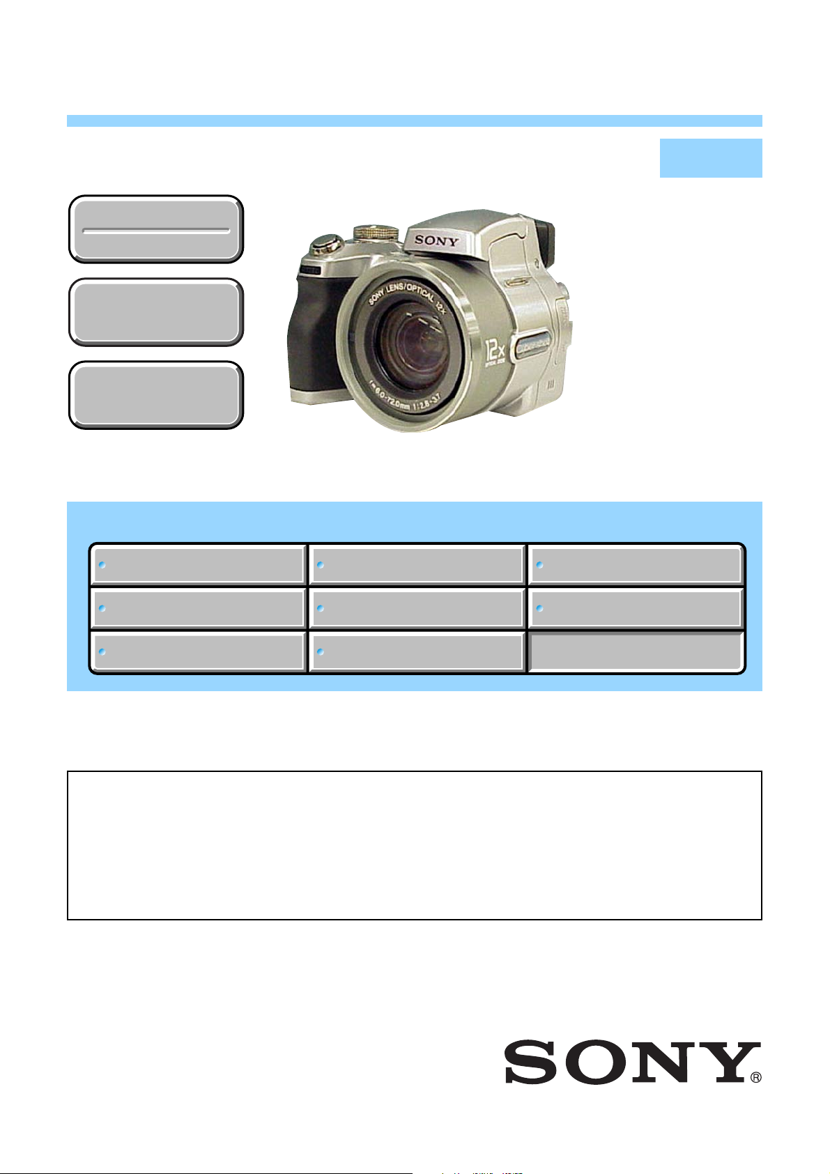
DSC-H1
SERVICE MANUAL
Ver. 1.4 2006. 06
Revision History
Revision History
How to use
How to use
Acrobat Reader
Acrobat Reader
Internal memory
Internal memory
ON BOARD
ON BOARD
Link
Link
SPECIFICATIONS
SPECIFICATIONS
BLOCK DIAGRAMS
BLOCK DIAGRAMS
LEVEL 2
DSC-H1
US Model
Canadian Model
AEP Model
UK Model
Hong Kong Model
Australian Model
Japanese Model
PRINTED WIRING BOARDS
PRINTED WIRING BOARDS
E Model
Chinese Model
Korea Model
Tourist Model
SERVICE NOTE
SERVICE NOTE
DISASSEMBLY
DISASSEMBLY
• For ADJUSTMENTS (SECTION 6), refer to SERVICE MANUAL, ADJ (9-876-880-51).
• For INSTRUCTION MANUAL, refer to SERVICE MANUAL, LEVEL 1 (9-876-880-41).
• Reference number search on printed wiring boards is available.
On the CH-169 and SY-127 board
This service manual provides the information that is premised the circuit board replacement service and not intended repair
inside the SY-127 board.
Therefore, schematic diagram, printed wiring board, mounted parts location and electrical parts list of the
shown.
The following pages are not shown.
Schematic diagram .............................Pages 4-21 to 4-44
Printed wiring board ............................Pages 4-55 to 4-60
Waveforms ........................................... Page 4-62
FRAME SCHEMATIC DIAGRAMS
FRAME SCHEMATIC DIAGRAMS
SCHEMATIC DIAGRAMS
SCHEMATIC DIAGRAMS
Mounted parts location .............................
Electrical parts list ................................... Pages 5-14 to 5-18
REPAIR PARTS LIST
REPAIR PARTS LIST
SY-127
Page 4-64
board are not
DIGITAL STILL CAMERA
DSC-H1
9-876-880-31
Sony EMCS Co.
2006F1600-1
©2006.06
Published by Kohda TEC
Page 2

SPECIFICATIONS
Camera
[System]
Image device 7.19 mm (1/2.5 type) color
CCD, Primary color filter
Total pixel number of camera
Approx. 5 255 000 pixels
Effective pixel number of camera
Approx. 5 127 000 pixels
Lens 12 zoom lens
f = 6.0 - 72.0 mm (36 - 432 mm
when converted to a 35 mm still
camera)
F2.8 - 3.7
Exposure control Automatic exposure, Shutter
speed priority, Aperture
priority, Manual exposure,
Scene Selection (7 modes)
White balance Automatic, Daylight, Cloudy,
Fluorescent, Incandescent,
Flash, One push
File format (DCF compliant)
Still images: Exif Ver. 2.2
JPEG compliant, DPOF
compatible
Movies: MPEG1 compliant
(Monaural)
Recording media Internal memory 32 MB
“Memory Stick”
Flash Recommended distance (ISO
set to Auto): 0.3 m to 6.8 m
(11 26/32 inches to 22 feet
3 23/32 inches) (W)/0.9 m to
5.2 m (2 feet 11 14/32 inches to
17 feet 23/32 inches) (T)
Viewfinder Electric viewfinder (color)
[Input and Output connectors]
A/V OUT (MONO) jack (Monaural)
Minijack
Video: 1 Vp-p, 75 ,
unbalanced, sync negative
Audio: 327 mV (at a 47 k
load)
Output impedance 2.2 k
USB jack mini-B
USB communication
Hi-Speed USB (USB 2.0
compliant)
[LCD screen]
LCD panel 6.2 cm (2.5 type) TFT drive
Total number of dots
115 200 (480x240) dots
[Finder]
LCD panel 0.75 cm (0.3 type) TFT drive
Total number of dots
115 200 (480x240) dots
[Power, general]
Power HR 15/51:HR6 (size AA)
Nickel-Metal Hydride batteries
(2), 2.4 V
ZR6 (size AA) Oxy Nickel
Primary Battery (2, not
supplied), 3 V
AC-LS5K AC Adaptor (not
supplied), 4.2 V
Power consumption
(during shooting with the LCD screen)
1.8 W
Operating temperature
0°C to +40°C (+32°F to
+104°F)
Storage temperature
–20°C to +60°C (–4°F to
+140°F)
Dimensions 108x81.4x91.2 mm
(4 1/4x 31/4x 35/8 inches)
(W/H/D, excluding maximum
protrusions)
Mass Approx. 590.8 g (1 lb 20.8 oz)
(including two batterries,
shoulder strap, adaptor ring,
lens hood, lens cap, etc.)
Microphone Electret condenser microphone
Speaker Dynamic speaker
Exif Print Compatible
PRINT Image Matching III
Compatible
PictBridge Compatible
BC-CS2A/CS2B Ni-MH battery charger
Power requirements
AC 100 to 240 V, 50/60 Hz,
3 W
Output voltage AA: DC 1.4V 400 mAx 2
AAA: DC 1.4 V 160 mAx2
Operating temperature
0°C to +40°C (+32°F to
+104°F)
Storage temperature
–20°C to +60°C (–4°F to
+140°F)
Dimensions Approx. 71x30x91 mm
(2 7/8x 13/16x 35/8 inches)
(W/H/D)
Mass Approx. 90 g (3 oz)
Design and specifications are subject to change
without notice.
DSC-H1
— 2 —
Page 3

SAFETY CHECK-OUT
After correcting the original service problem, perform the following
safety checks before releasing the set to the customer.
1. Check the area of your repair for unsoldered or poorly-soldered
connections. Check the entire board surface for solder splashes
and bridges.
2. Check the interboard wiring to ensure that no wires are
"pinched" or contact high-wattage resistors.
3. Look for unauthorized replacement parts, particularly
transistors, that were installed during a previous repair . Point
them out to the customer and recommend their replacement.
4. Look for parts which, through functioning, show obvious signs
of deterioration. Point them out to the customer and
recommend their replacement.
5. Check the B+ voltage to see it is at the values specified.
6. Flexible Circuit Board Repairing
• Keep the temperature of the soldering iron around 270˚C
during repairing.
• Do not touch the soldering iron on the same conductor of the
circuit board (within 3 times).
• Be careful not to apply force on the conductor when soldering
or unsoldering.
SAFETY-RELATED COMPONENT WARNING!!
COMPONENTS IDENTIFIED BY MARK 0 OR DOTTED LINE WITH
MARK 0 ON THE SCHEMATIC DIAGRAMS AND IN THE PARTS
LIST ARE CRITICAL TO SAFE OPERATION. REPLACE THESE
COMPONENTS WITH SONY PARTS WHOSE PART NUMBERS
APPEAR AS SHOWN IN THIS MANUAL OR IN SUPPLEMENTS
PUBLISHED BY SONY .
Unleaded solder
Boards requiring use of unleaded solder are printed with the leadfree mark (LF) indicating the solder contains no lead.
(Caution: Some printed circuit boards may not come printed with
the lead free mark due to their particular size.)
: LEAD FREE MARK
Unleaded solder has the following characteristics.
• Unleaded solder melts at a temperature about 40°C higher than
ordinary solder.
Ordinary soldering irons can be used but the iron tip has to be
applied to the solder joint for a slightly longer time.
Soldering irons using a temperature regulator should be set to
about 350°C.
Caution: The printed pattern (copper foil) may peel away if the
heated tip is applied for too long, so be careful!
• Strong viscosity
Unleaded solder is more viscous (sticky , less prone to flow) than
ordinary solder so use caution not to let solder bridges occur such
as on IC pins, etc.
• Usable with ordinary solder
It is best to use only unleaded solder but unleaded solder may
also be added to ordinary solder.
ATTENTION AU COMPOSANT AYANT RAPPORT
À LA SÉCURITÉ!
LES COMPOSANTS IDENTIFÉS P AR UNE MARQUE 0 SUR LES
DIAGRAMMES SCHÉMA TIQUES ET LA LISTE DES PIÈCES SONT
CRITIQUES POUR LA SÉCURITÉ DE FONCTIONNEMENT. NE
REMPLACER CES COMPOSANTS QUE PAR DES PIÈSES SONY
DONT LES NUMÉROS SONT DONNÉS DANS CE MANUEL OU
DANS LES SUPPÉMENTS PUBLIÉS PAR SONY.
CAUTION :
Danger of explosion if battery is incorrectly replaced.
Replace only with the same or equivalent type.
DSC-H1
— 3 —
Page 4

TABLE OF CONTENTS
1. SERVICE NOTE ........................................................ 1-1
2. DISASSEMBLY
2-1. DISASSEMBLY······························································2-1
2-2. SERVICE POSITION ·····················································2-5
2-3. CIRCUIT BOARDS LOCATION ···································2-7
2-4. FLEXIBLE BOARDS LOCATION ································2-8
HELP (List of caution points is shown here.)
3. BLOCK DIAGRAMS
3-1. OVERALL BLOCK DIAGRAM (1/2) ··························· 3-1
3-2. OVERALL BLOCK DIAGRAM (2/2) ··························· 3-3
3-3. POWER BLOCK DIAGRAM (1/2) ································ 3-5
3-4. POWER BLOCK DIAGRAM (2/2) ································ 3-7
4. PRINTED WIRING BOARDS AND
SCHEMATIC DIAGRAMS
4-1. FRAME SCHEMATIC DIAGRAM································4-1
4-2. SCHEMATIC DIAGRAMS
• CD-576 (CCD IMAGER)
SCHEMATIC DIAGRAM ······························4-5
• MS-275 (MEMORY STICK, LI BATTERY)
SCHEMATIC DIAGRAM ······························4-7
• ST-123 (FLASH DRIVE)
SCHEMATIC DIAGRAM ······························4-9
• ST-124 (FLASH)
SCHEMATIC DIAGRAM ····························4-17
• PL-039 (PLUNGER)
SCHEMATIC DIAGRAM ······························4-8
• SW-447 (1/2) (FUNCTION SW)
SCHEMATIC DIAGRAM ····························4-11
• SW-447 (2/2) (PITCH/YAW SENSOR AMP)
SCHEMATIC DIAGRAM ····························4-13
• EV-016 (EVF, BACK LIGHT)
SCHEMATIC DIAGRAM ······························4-7
• AF-102 FLEXIBLE (AF LED, LENS COVER SW)
SCHEMATIC DIAGRAM ····························4-15
• SW-006 FLEXIBLE (SY-SW RELAY)
SCHEMATIC DIAGRAM ····························4-18
• MS-029 FLEXIBLE (SY-MS RELAY)
SCHEMATIC DIAGRAM ····························4-15
• ST-001 FLEXIBLE (SY-ST RELAY)
SCHEMATIC DIAGRAM ····························4-17
• FP-224 FLEXIBLE (SY-CD RELAY)
SCHEMATIC DIAGRAM ····························4-16
• CONTROL SWITCH BLOCK (SW51780)
SCHEMATIC DIAGRAM ····························4-19
Shematic diagram of the CH-169 and SY-127 board
are not shown.
Pages from 4-21 to 4-44 are not shown.
4-3. PRINTED WIRING BOARDS
• CD-576 (CCD IMAGER)
PRINTED WIRING BOARD ·······················4-49
• MS-275 (MEMORY STICK, LI BATTERY)
PRINTED WIRING BOARD ·······················4-47
• ST-123 (FLASH DRIVE)
PRINTED WIRING BOARD ·······················4-51
• ST-124 (FLASH)
PRINTED WIRING BOARD ·······················4-52
• PL-039 (PLUNGER)
PRINTED WIRING BOARD ·······················4-51
• SW-447 (FUNCTION SW, PITCH/YAW SENSOR AMP)
PRINTED WIRING BOARD ·······················4-53
• EV-016 (EVF, BACK LIGHT)
PRINTED WIRING BOARD ·······················4-49
• AF-102 FLEXIBLE (AF LED, LENS COVER SW)
PRINTED WIRING BOARD ·······················4-47
Printed wiring board of the CH-169 and SY-127 board
are not shown.
Pages from 4-55 to 4-60 are not shown.
4-4. WAVEFORMS ······························································4-61
Wav eforms of the SY -127 board are not shown.
Page 4-62 is not shown.
4-5. MOUNTED PARTS LOCATION ·································4-63
Mounted parts location of the SY-127 board is not
shown.
Page 4-64 is not shown.
5. REPAIR PARTS LIST
5-1. EXPLODED VIEWS ······················································ 5-3
5-1-1. OVERALL SECTION····················································5-3
5-1-2. LED SECTION, CABINET(REAR) SECTION ············5-4
5-1-3. MAIN SECTION ···························································5-5
5-1-4. EVF SECTON ·······························································5-6
5-1-5. LENS SECTION ···························································5-7
5-1-6. CABINET(FRONT) SECTION·····································5-8
5-1-7. ST SECTION ·································································5-9
Checking supplied accessories ················································5-10
5-2. ELECTRICAL PARTS LIST ········································5-11
Electrical parts list of the SY-127 board are not
shown.
Pages from 5-14 to 5-18 are not shown.
DSC-H1
— 4 —
Page 5

• NOTE FOR REPAIR
1. SERVICE NOTE
Make sure that the flat cable and flexible board are not cracked of
bent at the terminal.
Do not insert the cable insufficiently nor crookedly.
Cut and remove the part of gilt
which comes off at the point.
(Take care that there are
some pieces of gilt left inside)
When remove a connector, don't pull at wire of connector.
Be in danger of the snapping of a wire.
When installing a connector, don't press down at wire of connector.
Be in danger of the snapping of a wire.
[Discharging of the FLASH unit’s charging capacitor]
The charging capacitor of the FLASH unit is charged up to the
maximum 300 V potential.
There is a danger of electric shock by this high voltage when the
capacitor is handled by hand. The electric shock is caused by the
charged voltage which is kept without discharging when the main
power of the DSC-H1 is simply turned off. Therefore, the remaining
voltage must be discharged as described below.
Preparing the Short Jig
To preparing the short jig. a small clip is attached to each end of a
resistor of 1 kΩ /1 W (1-215-869-11)
Wrap insulating tape fully around the leads of the resistor to prevent
electrical shock.
Discharging the Capacitor
1 Remove the main section.
2 Discharge the capacitor on the ST -123 board for about 10 seconds
by using the short jig.
Caution
1
Discharging the capacitor
Capacitor
1 kΩ/1 W
Wrap insulating tape.
DSC-H1
1-1
Short jig (
ST-123 board
1kΩ/1W
)
Page 6
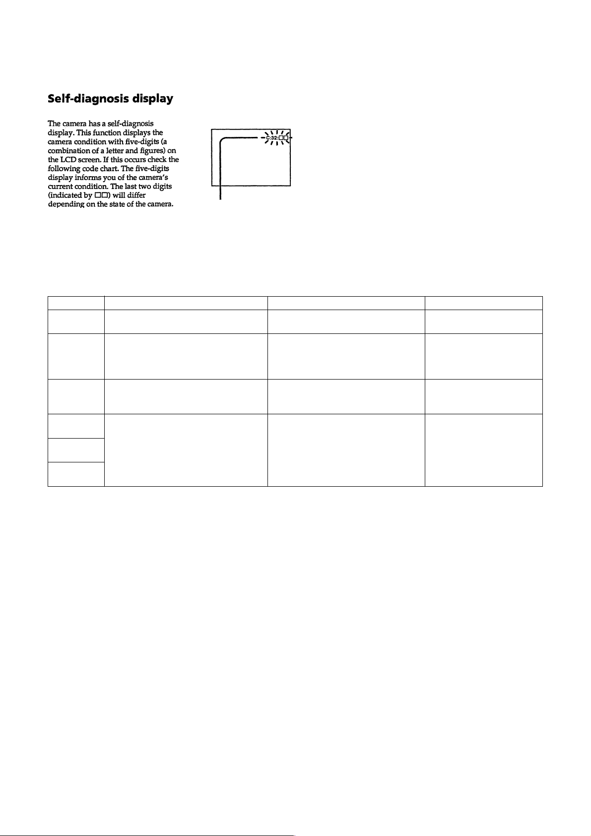
[Description on Self-diagnosis Display]
Self-diagnosis display
• C: ss: ss
The contents which can be handled
by customer, are displayed.
• E: ss: ss
The contents which can be handled
by engineer, are displayed.
Display Code
C:32:01
C:13:01
E:91:01
E:01:XX
E:61:00 *1
E:61:10 *1
Note : The error code is cleared if the battery is removed, except defective flash unit.
*1: The error display is given in two ways.
Turn off the main power then back on.
Replace the memory stick.
Format the memory stick with the DSC-H1.
Checking of flash unit or replacement of
flash unit.
Checking of lens drive circuit
Countermeasure
Trouble with hardware.
• The type of memory stick that cannot be
used by this machine, is inserted.
• Data is damaged.
• Unformatted memory stick is inserted.
Abnormality when flash is being
charged.
When failed in the focus initialization.
Cause
Caution Display During Error
SYSTEM ERROR
MS ERROR
Flash LED
Flash display
Flashing at 3.2 Hz
—
DSC-H1
1-2
Page 7
• METHOD FOR COPYING OR ERASING THE DATA IN INTERNAL MEMORY
p
The data can be copied/erased by the operations on the Setup screen. (When erasing the data, execute formatting the internal memory.)
Note: 1 When replacing the SY-127 board, erase the data in internal memory of the board before replacement.
Note: 2 When replacing the SY-127 board or the IC381 on the SY-127 board, execute formatting and initialize the internal memory after
replacement.
Method for Copying the Data in Internal Memory
Copy
Copies all images in the internal memory to a “Memory Stick”.
OK
Cancel
1 Insert a “Memory Stick” having 32 MB or larger capacity.
2 Select [OK] with v on the control button, then press z.
The message “All data in internal memory will be copied Ready?” appears.
3 Select [OK] with v , then pr es s z.
Copying starts.
Copying
102_COPY
Use batteries with enough capacity or the AC Adaptor (not supplied). If you attempt to copy image files
using batteries with little remaining capacity, the batteries may run out, causing copying to fail or possibly
corrupting the data.
You cannot copy individual images.
The original images in the internal memory are retained even after copying. To delete the contents of the
internal memory, remove the “Memory Stick” after copying, then execute the [Format] command in
Internal Memory Tool.
You cannot select a folder copied on a “Memory Stick”.
The setting of (Print order) marks is not copied even when you copy data.
See the following procedure.
Cancels the copying.
Method for Formatting the Internal Memory
Format
Formats the internal memory.
Note that formatting irrevocably erases all data in the internal memory, including even protected images.
OK
Cancel
1 Select [OK] with v on the control button, then press z.
The message “All d ata in internal memory will be erased Ready?” appears.
2 Select [OK] with v, then press z.
The format is com
lete.
See the following procedure.
Cancels the formatting.
• PROCESS AFTER FIXING FLASH ERROR
When “FLASH error” (Self-diagnosis Code E : 91 : ** ) occurs, to prevent any abnormal situation caused by high voltage, setting of the
flash is changed automatically to disabling charge and flash setting.
After fixing, this setting needs to be deactivated. Flash error code can be initialized by the operations on the Setup screen.
Method for Initializing the Flash Error Code
Initialize
Initializes the setting to the default setting.
OK
Cancel
See the following procedure.
Cancels the resetting.
DSC-H1
1 Select [OK] with v on the control button, then press z.
The message “Initialize all settings Ready?” appears.
2 Select [OK] with v, then press z.
The settings are reset to the default setting.
Make sure that the power is not disconnected during resetting.
1-3E
Page 8
The following flow chart shows the disassembly procedure.
2-1. DISASSEMBLY
2. DISASSEMBLY
2
1
Three screws (M2x4) silver
2
Three screws (M2x4) silver
3
Remove the JK lid in the
direction of the arrow.
4
Claw
5
Cabinet (rear) section
1
EV-016 board
2
T wo claws
3
EVF section
4
5
4
1
3
1
3
1
Light guide plate (2.5) block
2
T wo claws
3
Remove the LCD, Light guide plate (2.5) block
in the direction of the arrow.
4
LCD unit
5
LCD unit, Light guide plate (2.5) block
6
2
1
5
3
Note:
Be very careful not to
damage the flexible board.
5
SY-127
1
Tapping screw (M1.7x4) black
2
Three claws
3
Claw
4
LCD frame assembly
3
4
2
1
1
Flexible flat cable (MS-029)
2
Battery connector
3
From the loudspeaker
4
Three tapping screws (M1.7x4) black
5
Fuse replacement caution label
6
SY-127 board
1
Flexible flat cable (MS-029)
2
Tapping screw (M1.7x4) black
3
T wo claws
4
MS-275 board
5
Battery connector
6
Three claws
7
Battery terminal board
3
SY-127
9
8
1
From the lens flexible board
2
FP-224 flexible board
3
From the lens flexible board
4
Flexible flat cable (ST-001)
5
Control switch block (SW51780)
6
AF-102 flexible board
7
From the microphone
8
Tapping screw (M1.7x4) black
9
Main section
ST section
(See page 2-3.)
3
SY-127
1
1
Flexible flat cable (SW-006)
2
Four tapping screws (M1.7x4) black
3
Claw
4
SW-447 board
-447
SW
2
4
M
S-275
2
4
3
1
SY-127
2
2
SY-127
6
7
5
4
3
7
1
4
2
SY -127
1
2
6
SY -127
6
5
5
4
3
7
1
DSC-H1
2-1 2-2
Page 9

Caution
1
Discharging the capacitor
Capacitor
Short jig (
ST-123 board
1kΩ/1W
2. DISASSEMBLY
2. DISASSEMBLY
2
2
1
)
1
Two tapping screws (M1.7x4) black
2
Lens section
1
Tapping screw (M1.7x4) black
2
Control switch block (SW51780), Microphone unit
1
6
1
Tapping screw (M1.7x4) black
2
Claw
3
ST-123 board
4
Three harnesses (HA-001) (Red, White, Blue)
5
Open the ST cover in the direction of the arrow.
6
ST section
HELP 02
1
4
5
HELP 01
4
3
3
2
1
2
1
Remove the
AF-102 flexible board
in the direction of the arrow.
2
Three claws
3
Three claws
4
AF-102 flexible board
DSC-H1
2-3 2-4
Page 10
2-2. SERVICE POSITION
2
1
[SERVICE POSITION TO CHECK THE SY-127 BOARD]
From the lens section
SW-447 board
FP-224 flexible board
2
4
2
SW-447
Lens section
5
3
1
1
Flexible flat cable (SW-006)
Monitor TV
Audio/Video jack
CN401
CN502
MS-275
CN101
CN506
SY-127
CN514
CN513
SY-127 board
CN509
Battery terminal board
2
1
5
4
3
Caution
1
ST-123 board
Discharging the capacitor
Capacitor
Short jig (
1kΩ/1W
From the lens section
)
Flexible flat cable (MS-029)
MS-275 board
1
7
2
1
-
Y
3
S
4
3
7
2
1
-
Y
S
1
6
4
3
2
7
1
2
1
7
4
4
-
W
S
2
4
5
9
7
2
1
-
Y
S
8
3
Flexible flat cable (MS-029)
2
7
2
-1
Y
S
3
1
27
-1
Y
S
MS-275 board
6
5
4
Control switch block (SW51780)
Insert the batteries (size AA).
Battery section
Nickel Metal Hydride batteries (x2).
2
DSC-H1
2-5 2-6
Page 11
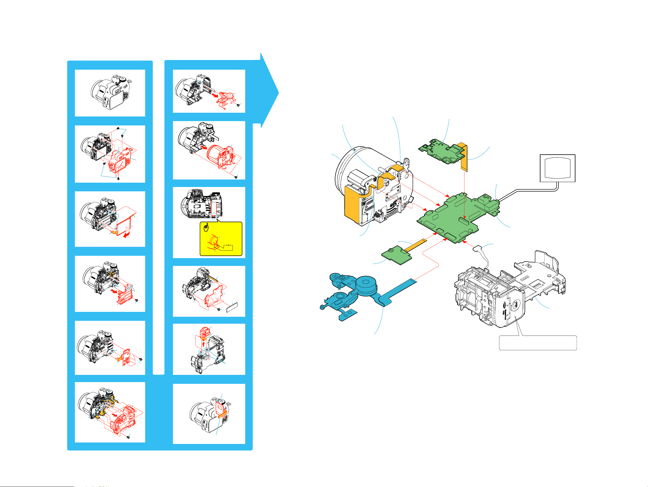
2-3. CIRCUIT BOARDS LOCATION
2. DISASSEMBLY
2. DISASSEMBLY
PL-039
CD-576
ST-124
AF-102
ST-123
MS-275
SW-447
CH-169
SY-127
EV-016
NAME
AF-102 AF LED, LENS COVER SW
CD-576
CH-169
EV-016
MS-275
PL-039
ST-123
ST-124
SW-447
SY-127
CCD IMAGER
CCD SIGNAL PROCESS
EVF, BACK LIGHT
MEMORY STICK, LI BATTERY
PLUNGER
FLASH DRIVE
FLASH
FUNCTION SW, PITCH/YAW SENSOR AMP
LENS DRIVE, CAMERA A/D CONV., TIMING GENERATOR, CAMERA DSP,
SYSTEM CONTROL, 256Mbit SDRAM, FLASH MEMORY, SUPER AND FLASH MEMORY,
A/V AMP, USB/AV JACK, SP, MIC, PANEL DRIVE, STEADY SHOT CONTROL,
LENS SERVO, CONNECTOR, DC/DC CONVERTER
FUNCTION
DSC-H1
2-7
Page 12
2. DISASSEMBLY
2. DISASSEMBLY
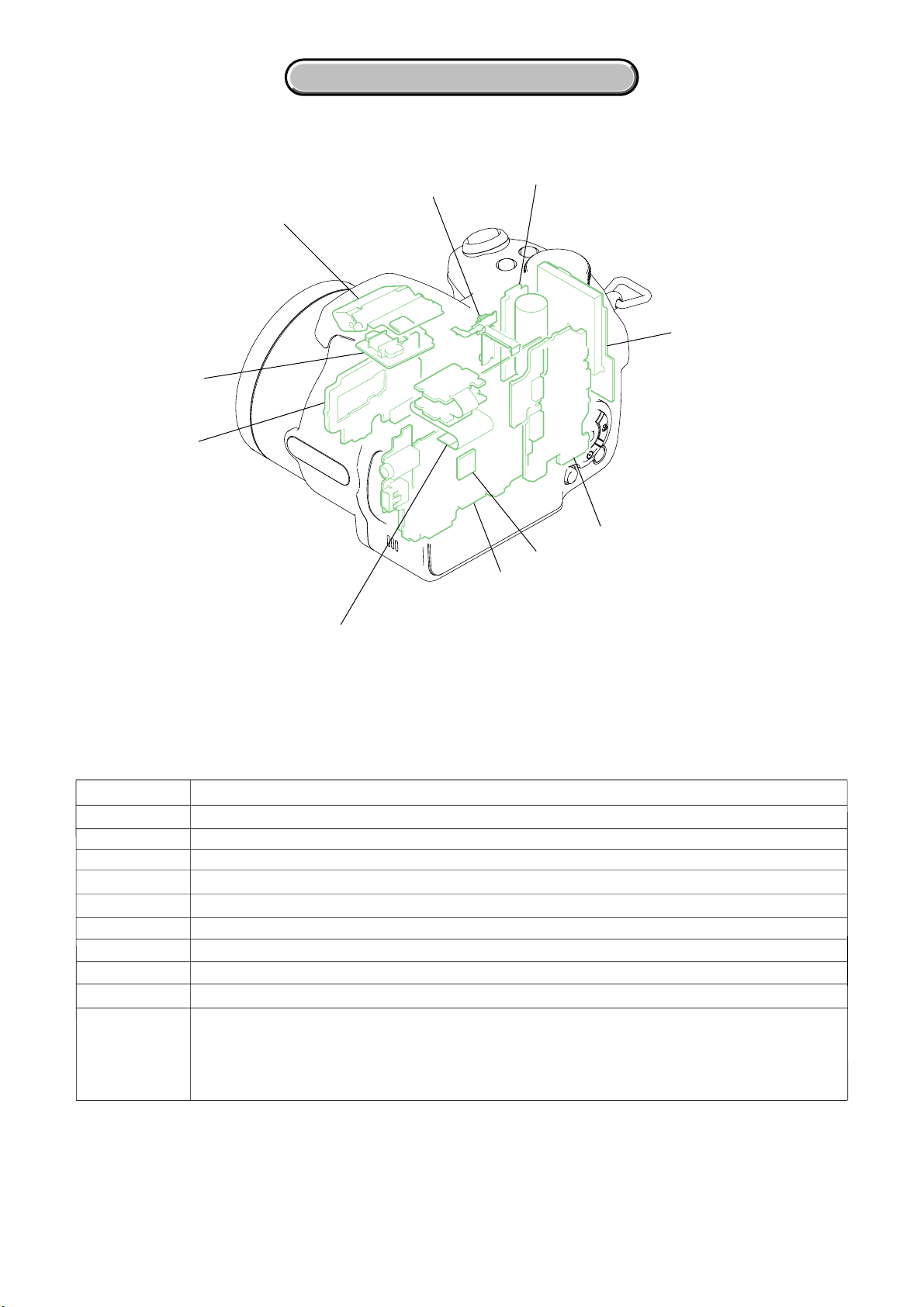
2-4. FLEXIBLE BOARDS LOCATION
The flexible boards contained in the optical unit are not shown.
CONTROL SWITCH BLOCK (SW51780)
MS-029
SW-006
FP-224
ST-001
DSC-H1
2-8E
Page 13

HELP 01
HELP 02
HELP
Disassembling and assembling procedures that require attention are described here.
Harness (HA-001) (Blue)
Harness (HA-001) (White)
Harness (HA-001) (Red)
6
7
2
White
8
1
9
Blue
Red
White
Red
3
Blue
4
5
1
Harness (H-001) (Red)
2
Harness (H-001) (White)
3
Harness (H-001) (
4
Apply the soldering in three points.
5
ST-123 board
6
ST-124 board
7
Four
claws
8
ST cover
9
Tapping screw (M1.7x4) black
0
ST section
0
Blue
)
DSC-H1
HELP
Page 14

Link
Link
3. BLOCK DIAGRAMS
OVERALL BLOCK DIAGRAM (1/2)
OVERALL BLOCK DIAGRAM (2/2)
POWER BLOCK DIAGRAM (1/2)
POWER BLOCK DIAGRAM (2/2)
DSC-H1
Page 15

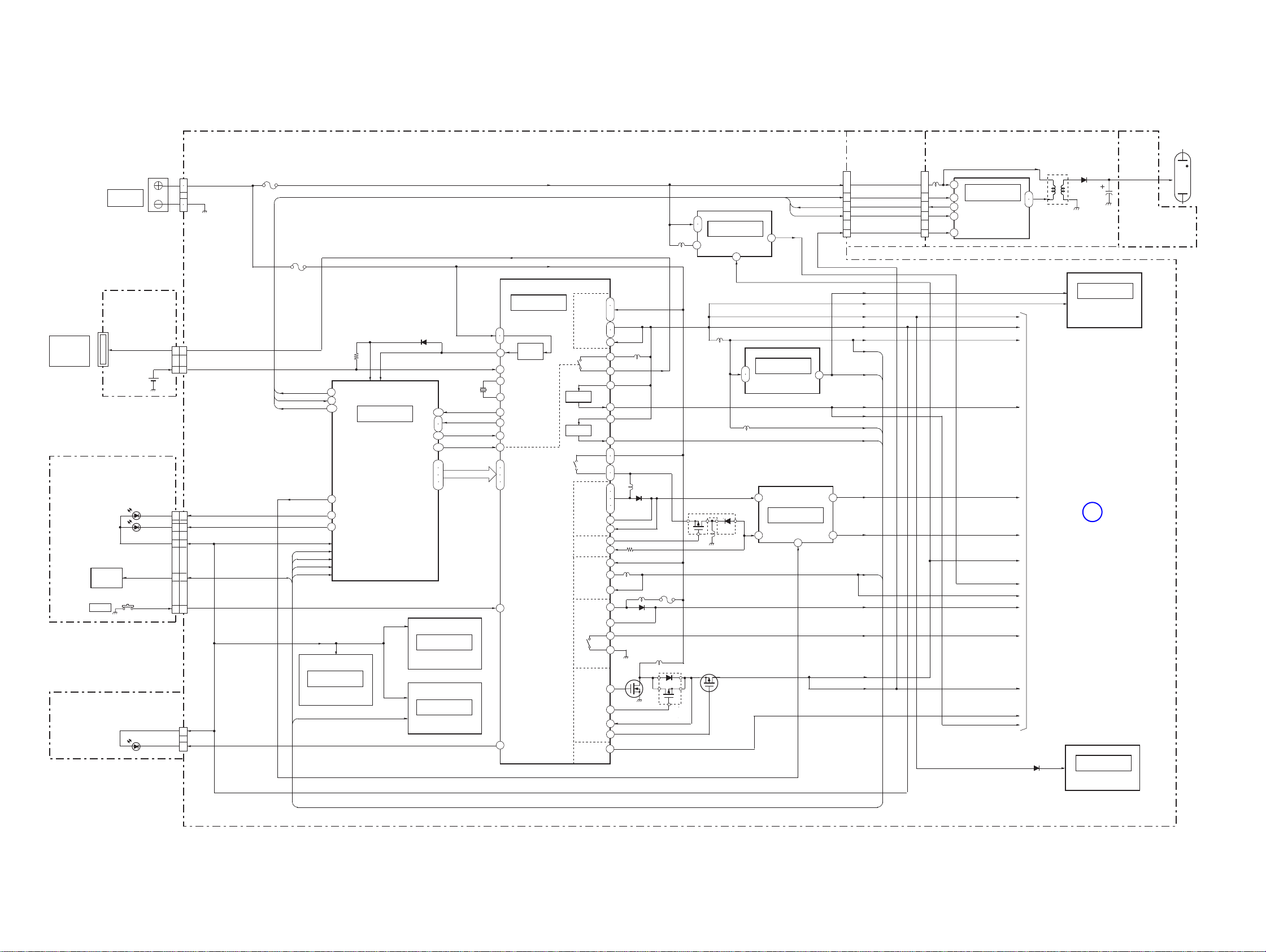
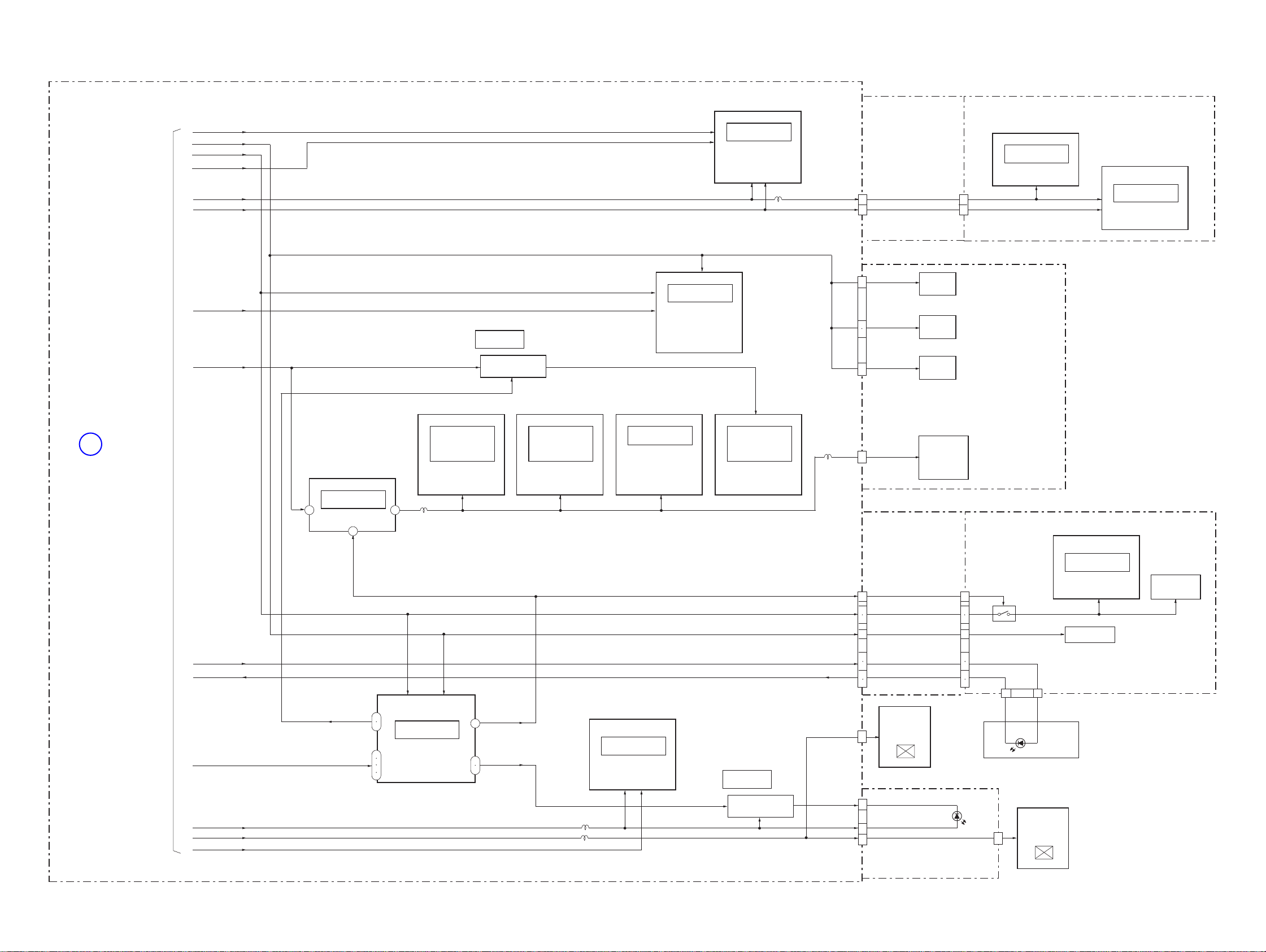
3-1. OVERALL BLOCK DIAGRAM (1/2)
3. BLOCK DIAGRAMS
Ver 1.1 2005. 09
( ) : Number in parenthesis ( ) indicates the division number of schematic diagram where the component is located.
LENS UNIT
ACTIVE
LENS
ACTUATOR
PITCH
YAW
SE401
PITCH
SENSOR
SE402
YAW
SENSOR
8
12
P DRIVE A
P DRIVE B
7
6
Y DRIVE A
8
Y DRIVE B
9
2
4
CN101
IC401
PITCH/YAW
SENSOR
AMP
IRIS
SHUTER
IRIS
MOTOR
M
SHUTTER
MOTOR
M
FOCUS
MOTOR
M
ZOOM
MOTOR
M
FOCUS RESET
SENSOR
ZOOM RESET
SENSOR 1ST
ZOOM RESET
SENSOR 2ND
ZOOM DC FG
7
6
7
6
(9/11)
IC103
PITCH DRIVE
(9/11)
IC102
YAW DRIVE
2
18
CN451
CD-576 BOARD
IRIS A
IRIS XA
IRIS B
IRIS XB
1
4
SHUTTER +
8
SHUTTER-
5
FOCUS A
FOCUS XA
FOCUS B
9
FOCUS XB
16
ZOOM +
36
ZOOM -
39
22
24
25
32
31
CN401
PITCH POS AD
YAW POS AD
PITCH AD
9
YAW AD
7
V1A,B
V2
V3A,B
V4
V5A,B
V6
V7A,B
V8,
VST,
VHLD
13
73
IC101
CCD IMAGER
1-14
25-38
25-38
F2
E2
D2
B1
F3
F4
D6
E6
B7
C6
B4
B5
(9/11)
IC104
PRE DRIVE
12
14
CN513
27,28
19-17
CN101
CN502
IC401
SHUTTER DRIVE
FOCUS MOTOR
X902
20MHz
H1A,B
H2A,B
RG
(1/11)
(1/2)
IRIS DRIVE
DRIVE
ZOOM MOTOR
DRIVE
2
FP-224 FLEXIBLE
BOARD
15
1
F5
E5
D3
F1
G1
E4
D5
A6
B6
C5
A2
B2
IC105
LPF LPF
876
131
132
129
130
(8/11)
1
IC901
3
STEADY SHOT
CONTROL
IC102
BUFFER
6
9
3
MSHUT DIR
MSHUT EN
FC DIR A
FC DIR B
ZM DIR A
ZM BRK A
FC SENS
ZM SENS 1ST
ZM SENS 2ND
ZM DC FG 1A
ZM DC FG 1B
7
(9/11)(9/11)
IC106
8
PITCH PWM
95
YAW PWM
96
66
65
63
EVF BL ON
37
EVF BL LEV
38
9
8
184
22
12
10
8
6
18
CN101
DIR2A
BRK2A
DIR2B
BRK2B
FC EN
XDD RST OUT
XSHIFT ON
SY-127 BOARD (1/2)
CCD OUT
6
22
12
10
1
8
|
6
5
18
CN502
7
|
20
(9/11)
IC101
PITCH PWM
3
442
(9/11)
IC107
12
SAN1 SO, SI, SCK
YAW PWM
2
S/H
A/D CONV.
(2/11)
CP201
TIMING
GENERATOR
40 41
SAN1 SO,SCK
D0-D15
22
|
35
47
45
46
42
F4
(5/11)
IC381
SUPER AND
FLASH MEMORY
A20,A21,A25
V LINE OUT
CA AD0 - CA AD13
CLK TGO
CA HD, CA FD
(4/11)
IC353
256Mbit
SDRAM
DIR2A
BRK2A
DIR2B
BRK2B
MSHUT DIR
MSHUT EN
FC DIR A
FC DIR B
FC EN
ZM DIR A
ZM BRK A
FC SENS
ZM SENS 1ST
ZM SENS 2ND
ZM DC FG 1A
ZM DC FG 1B
D0-D15
D0-D15
A01-A21,A25
5
IC802
X301
12MHz
XTAL OSC
(4/11)
IC351
FLASH MEMORY
(6/11)
VIDEO AMP
D0-D31
A0-A11
B5
A01-A21
K5,G4,H4,L5
H2,H1,J1,J2
M5,J4,K4,M6
K2,K1
EXTAL
A6
F2
E1
H5
J5
D21,D22,D20,B22,A22,A23
B23,E20,E21,B24,A24,A25
B25,C25,C26,B26,E10,A10
D10,E11,B10,A11,B11,E12
D11,D12,F12,B12,A12,E13
D17,D18,D16,B18,A19
B19,E16,D19,E19,E17
N4
P6
P4
R2
R25
R5
L2
N5
L4
N6
N2
U4
U5
V4
V5
W4
AB13,AA13,AE13,AF13,AF12
AE12,AA12,AC12,AC11,AB12
AE11,AF11,AE10,AB11,AC10
AF21,AF20,AE20,AB18,AB19
AC19,AB16,AE19,AF19,AF18
AE18,AA15,AC18,AC17,AB15
AE17,AF17,AE16,AB14,AC16
AC15,AE14,
V OUT
H26
3
AB10
D13,D14
B20,A20
(3/11)
IC301
(1/2)
CAMERA DSP
SAN1 SO, SI, SCK
AC4,AE4
AE5,AC5
AB6,AF6
D8,D7,E8
E7,D6,D5
E6,B4
E9
B8
D9
U2
T2
R6
AF4
L26
K26
AC1
AD1
T5
U25
LCD D0-D7
LCD HD
LCD VD
LCD CK
SAN1 SO, SI, SCK
XSAN RST OUT
AUIN
AUOUT
Q301
XAV JACK IN
MS D0-MS D3, MS BS, MS CLK
SAN1 SO, SCK
XMS IN
XSHIFT ON
XDD RST OUT
USB VBUS
SAN1 SO, SCK
B3,A3,B4
B5,A5,B6
A7,B7
EVF BL ON
EVF BL LEV
F3
E3
E6
C1
E5
A9
C9
A2
B9
A10
C10
IC801
SPEAKER AMP
(7/11)
IC601
RGB DRVE
TIMING
GENERATOR
(7/11)
IC602
EVF BACK LIGHT
DRIVE
TO
OVERALL
BLOCK DIAGRAM
(2/2)
(PAGE 3-4)
(6/11)
MIC AMP
AU OUT AMP
USB DPP, USB DMM
USB VBUS
B6
A5
A2
D1
C2
K2
K3
K1
J6
K4
J4,H1
H2,G1
G2,F1
F2,E2
D1,D2
C2,B1
J7
Q602,603
VR
VG
VB
PANEL COM/CS
PSIG
PANEL REF
XSTB E
PANEL VST
VCK,EN
DWN,XSTB M
PCG,HST
HCK2,HCK1
RGT
1
XMS IN
PANEL REF
PANEL VST
VCK,EN
DWN,XSTB E
PCG,HST
HCK2,HCK1
RGT
M 5V
CN506
PANEL REF
PANEL VST
DWN,XSTB M
PCG,HST
HCK2,HCK1
VR
VG
VB
EVF COM/CS
PSIG
EVF BL L
EVF BL H
V LINE OUT
AU LINE OUT
VCK,EN
CN505
RGT
CN508
CN510
CN511
3,2
6,5,7,
9,4,10
8
4
5
3
24
23
6
22
|
19
14
|
11
8
7
2
5
8
9
3
4
7
21
|
17
14
|
10
6
1
2
2
1
2
1
MS-029 FLEXIBLE
BOARD (1/2)
CN251
7,8,6,
4,9,3
5
MS-275
BOARD
(1/2)
LCD901
2.5 INCH
COLOR LCD
PANEL
CN001
EV-016
FLEXIBLE
BOARD
D001
(EVF BACK LIGHT)
MIC SIG
SP+
SP-
MIC
CN751
(USB)
J751
A/V OUT
MIC901
SP901
SPEAKER
17
18
16
21
19
20
15
|
5
4,3,5,7,2,8
6
LCD902
COLOR EVF
UNIT
CN252
MEMORY
STICK
CONNECTOR
SW-447 BOARD (1/2)
SW-006 FLEXIBLE
FLAT CABLE (1/2)
DSC-H1
3-1 3-2
Page 16

3-2. OVERALL BLOCK DIAGRAM (2/2)
Ver 1.1 2005. 09
( ) : Number in parenthesis ( ) indicates the division number of schematic diagram where the component is located.
BATTERY
TERMINAL
4
3
2
1
CN509
UNREG
REG GND
F001
F002
X001
32.768KHz
UNREG
MS-275
BOARD
(2/2)
BT251
LITHIUM
BATTERY
(SECONDARY)
DC/DC CONVERTER
REAL TIME CLOCK
A8
OSC I
OSC O
A9
B8
VL 3V
XPWR ON
C7
USB VBUS
C9
XMS IN
B10
CN251
(11/11)
IC001
(11/11)
IC005
-7,5V/15V REG
(11/11)
IC004
DC/DC CONV.
MS-029
FLEXIBLE
FLAT CABLE
(2/2)
SAN0 SO
SAN0 SI
XSAN0 SCK
BATT SENS
XDD RST OUT
XPWR OFF
VL 3V
C5
C6
B6
G5
A7
B7
A4
CN506
211
EVER 3.1V
EVER 2.8V
D 3.2V
D 3.2V (TO CAM)
D 3.2V (TO SP)
A 3.2V
MS VCC
CAM 2.9V (TO CAM)
CAM 2.9V (TO PANEL)
D 1.8V
M 5V
ST 5V
D 1.2V
PANEL 8.5V
BL H
BL L
XAF LED
CAM 15V
CAM -7.5V
STEADY 5V
SY-127 BOARD (2/2)
VL 3V
ST UNREG
SAN0 SO, SI, SCK
AB5
AA5
Y5
K25
Y4
R26
A23
SAN0 SO
SAN0 SI
XSAN0 SCK
BATT SENS
XDD RST OUT
XPWR OFF
(3/11)
IC301
(2/2)
SYSTEM CONTROL
STRB CHG
XSTRB FULL
STRB CHG CONT
STRB ON
STRB PLUNGER ON
XSTRB POPUP
XLENS COVER SENS
XAE LOCK SW
XSHUTTER SW
MODE DIAL 0
MODE DIAL 1
JOG A
JOG B
KEY AD2
XSTRB LED
XPWR LED
KEY AD0
KEY AD1
XACCESS LED
R22
V23
AB22
R4
AA25
V22
AC23
N21
P23
L22
L25
AB23
W22
G25
E22
D23
K23
L23
E4
1
IC401
A1
(2/2)
STRB PLUNGER DRIVE
TO
OVERALL
BLOCK DIAGRAM
(1/2)
(PAGE 3-2)
(1/11)
B3
XSHIFT ON
USB VBUS
XMS IN
XDD RST OUT
ST-001
FLEXIBLE
FLAT CABLE
12
|
10
STRB CHG
4
XSTRB FULL
5
STRB CHG CONT
6
STRB ON
AF-102 FLEXIBLE BOARD
XAF LED
S103
7
SHUTTER
8
1
MODE DIAL
3
5
6
4
EVF/LCD, FOCUS, BRK
14
12
XPWR ON
11
XSHIFT ON
9
BL H
BL L
CN501
CN507
CN514
CN513
7
8
7
5
1
4
8
7
14
12
10
9
11
1
3
4
6
20
19
1
5
4
3
2
SW-006
FLEXIBLE
FLAT CABLE
(1/2)
ST-123 BOARD FLASH UNIT
1
|
3
9
8
7
6
STRB PLUNGER
S001
(LENS COVER OPEN)
CN001
ST UNREG
15
10
9
6
4
D001 (AF LED)
HIGH VOLTAGE
CHAGER
IC001
IGBT
DRIVE
CN301
RY301
PLUNGER
(STRB POP UP)
4
3
1
PL-039 BOARD
D001
(RECT)
T001
1
2
7
S301
C004
Q001
FLASH
DRIVE
CONTROL SWITCH
BLOCK(SW51780)
S105
JOG DIAL
S106,101,102
STEADY SHOT
S104
POWER
S107
1
2
20
16
17
18
19
EXEC
D101 (FLASH)
D102 (POWER)
S458,460,456,454,457,453
DOWN, RIGHT, UP, LEFT, SET, DUST
S459,455,452,451
ZOOM WIDE, ZOOM TELE, MENU, DISPLAY
D455 (ACCESS)
CN451
CN452
LED901
LCD
BACK
LIGHT
6
4
SW-447 BOARD (2/2)
XE H
XE L
(ST-124
FLEXIBLE
BOARD)
L001
TRIGGER
COIL
D001
XENON
TUBE
DSC-H1
3-3 3-4
Page 17
3-3. POWER BLOCK DIAGRAM (1/2)
Ver 1.1 2005. 09
( ) : Number in parenthesis ( ) indicates the division number of schematic diagram where the component is located.
CN252
MEMORY
STICK
CONNECTOR
9
(SECONDARY)
CONTROL SWITCH
BLOCK (SW51780)
D102 (POWER)
D101 (FLASH)
MODE
DIAL
S104
POWER
AF-102 FLEXIBLE
BOARD
D001 (AF LED)
BATTERY
TERMINAL
MS-275
BOARD
MS VCC
BT251
LITHIUM
BATTERY
XPWR ON
VL 3V
D 3.2V
A 3.2V
CN251
D3.2V
XAF LED
SY-127 BOARD (1/2)
UNREG
4
3
REG GND
2
1
CN509
2
21111
CN506
3
12
1
14
2
13
13
2
4
11
CN514
3
4
CN507
F001
F002
STRB CHG
XSTRB FULL
STRB CHG CONT
-7.5V ON
D 3.2V
A 3.2V
AU 3.2V
VI 3.2V
D 1.2V
D 3.2V
R002
R22
V23
AB22
P25
D23
XPWR LED
E22
XSTRB LED
(5/11)
IC381
SUPER AND
FLASH MEMORY
D 1.8V
EVER 2.8V
EVER 3.1V
(3/11)
IC301
CAMERA DSP
SYSTEM CONTROL
D001
XCS DD
SAN0 SO
SAN0 SI
XSAN0 SCK
K25
Y4
R26
AA23
T25
W23
AB5
AA5
Y5
(4/11)
IC353
256Mbit
SDRAM
(4/11)
IC351
FLASH MEMORY
X001
32.768KHz
BATT SENS
XDD RST OUT
XPWR OFF
MS PWR ON
XPWR ON
ST UNREG
MS VCC
UNREG
(11/11)
IC001
DC/DC CONVERTER
REAL TIME CLOCK
J1
UNREG1-1,2
K1
3.1V
LDO1
H1
VL 3V
REG.
B8
RTC BAT
A8
OSC I
A9
OSC O
G5
UNREGMON
A7
XRESET
B7
XPWR OFF
MS PWR ON
D3
XCS DD
A6
SAN0 SO
C5
SAN0 SI
C6
XSAN0 SCK
B6
XPWRON1
C7
A4
XAF LED
-7.5V ON
D 3.2V
A 3.2V, AU 3.2V, VI 3.2V, D 1.8V, D 1.2V
2.9V REG
1.8V REG
PWR1-1
PWR1-2
PWR1-3
VO1-1
VO1-2
MS PWR IN
MS PWR
LDO3IN
LDO3
LDO2IN
LDO2
UNREG2
PWR56 OUT
LX5-1
LX5-2
LX5-3
LX5-4
RS3
TG4
PSG4
VO7
ST-001
FLEXIBLE
FLAT CABLE
12
ST UNREG
STRB CHG
XSTRB FULL
STEADY 5V
2
(6/11)
3.2V REG
(11/11)
15V REG
IC005
-7.5V REG
1
-7.5V ON
STRB CHG CONT
(11/11)
6
8
L010
A1
B1
C2
F1
F2
H2VFB1
L011
G1
MS VCC
G2
B2
A2
B3
A3
J6
K6
J7
K7
L006
J9
J10
K9
D003
K10
(RECT)
H10
VO5
H9VFB5
H6GT6
H7VFB6
D10PWR2
L003
C10LX2
D8VFB2
E10LX3
E9VO3
LV3
F9
F8
Q001
SWITCHING
G9BG4
F10
F7VFB4
G8
PANEL 8.5V
K4
L005
D002
(RECT)
Q002
RECT
F003
L008
IC004
DC/DC CONV.
9
L001
Q004
SWITCHING & RECT
L009
BL H
BL L
Q003
SWITCH
1
MT 5V
IC803
4
3
L803
3
|
10
4
5
6
ST 5V
9
CN501
AU 3.2V
D 3.2V (TO SP)
D 3.2V (TO CAM) D 3.2V (TO CAM)
D 3.2V
A 3.2V
AU 3.2V
1
CAM 2.9V
VI 3.2V
D 1.8V
67
4
D 1.2V
M 5V
ST 5V
ST-123 BOARD
1
|
15
3
L001
10
9
8
9
6
7
3
4
CN001
IC001
HIGH VOLTAGE
CHAGER
IGBT DRIVE
CAM 2.9VCAM 2.9V
CAM 15V
CAM -7.5V
M 5V
STEADY 5V
D 1.2V
BL H
BL L
ST 5V
PANEL 8.5V
CAM 2.9V (TO PANEL)
CAM 3.2V
D 3.2V
A 3.2V
T001
1
2
TO
POWER
BLOCK DIAGRAM
(2/2)
(PAGE 3-7)
D821
D001
(RECT)
C004
(6/11)
IC801
MIC AMP
SPEAKER AMP
AU OUT AMP
1
(6/11)
IC802
VIDEO AMP
XE H
FLASH UNIT
(ST-124
FLEXIBLE BOARD)
XENON
TUBE
DSC-H1
3-5 3-6
Page 18
3-4. POWER BLOCK DIAGRAM (2/2)
Ver 1.1 2005. 09
( ) : Number in parenthesis ( ) indicates the division number of schematic diagram where the component is located.
SY-127 BOARD (2/2)
1
TO
POWER
BLOCK DIAGRAM
(1/2)
(PAGE 3-6)
D 3.2V
D 3.2V
A 3.2V
CAM 2.9V
CAM 15V
CAM -7.5V
M 5V
STEADY 5V
CD-576 BOARD
IC102
BUFFER
16
14
CN101
LENS UNIT
IC101
CCD IMAGER
FULL PWR
LIM PWR
(9/11)
IC101
IC107
INVERTER
(9/11)
IC110
CURRENT
LIMITER
D 3.2V
(1/11)
IC401
IRIS DRIVE
SHUTTER DRIVE
FOCUS MOTOR DRIVE
ZOOM MOTOR DRIVE
Q107,110
VCC
(9/11) (9/11) (9/11)
IC105
IC104
IC106
LPF
PLUNGER DRIVE
PRE DRIVE
(2/11)
CP201
S/H
A/D CONV.
TIMING GENERATOR
L201
IC102
IC103
PITCH DRIVE
YAW DRIVE
CAM 15V CD
CAM -7.5V
CN401
L101
CN502
CN101
FP-224
FLEXIBLE
BOARD
16
14
21
27
28
33
3
FC RST VCC
ZM RST VCC
ZM FG VCC
A 4.6V
FOCUS
RESET
SENSOR
ZOOM
RESET
SENSOR
ZOOM
DC FG
ACTIVE
LENS
ACTUATOR
(9/11)
IC108
3
4.6V REG
4
A 3.2V
D 3.2V
1
VAP DD ON
L103
A 4.6V
SW-006
FLEXIBLE
FLAT CABLE
10
9
8
18
VAP DD ON
A 3.2V
D 3.2V
SW-447
BOARD
11
12
13
3
Q401,402
(2/2)
IC401
PITCH/YAW
SENSOR AMP
D455
ACCESS LED
SE401, 402
PITCH/YAW
SENSOR
DSC-H1
BL H
BL L
D_1.2V
ST 5V
PANEL 8.5V
CAM_ 2.9V(TO PANEL)
FULL PWR
LIM PWR
5
4
3
2
CN513
154
155
79
36
191
160
(8/11)
IC901
STEADY SHOT
CONTROL
170
37
38
VAP DD ON
EVF BL ON
EVF BL LEV
L603
L602
(7/11)
IC601
RGB DRIVE
TIMING
GENERATOR
EVF BL ON
EVF BL LEV
(7/11)
IC602
BACK LIGHT
DRIVE
Q602, 603
PANEL VDD
EVF BL L
EVF BL H
PANEL VDD
CN505
CN508
18
1
2
16
LCD901
2.5 INCH
COLOR LCD
PANEL
EV-016
BL H
BL L
D001 (EVF BACK LIGHT)
FLEXIBLE BOARD
3-7 3-8E
16
17
18
19
CN451
CN001
46
2
CN452
BACK
LIGHT
LCD902
COLOR EVF
UNIT
LED901
LCD
Page 19

4-1. FRAME SCHEMATIC DIAGRAM
4. PRINTED WIRING BOARDS AND SCHEMATIC DIAGRAMS
Ver 1.1 2005. 09
RGT
DWN
HCK1
73 198
123456789
N.C.
HST
VDD
HCK2
REG_GND
EVF_VSSG
CN452
1 N.C.
2 N.C.
3 N.C.
4 BL_L
5 N.C.
6 BL_H
6P
1
2
6 14 165
A
B
C
21
D
E
AV
COM
PSIG
COLOR EVF UNIT
B
G
R
CS
EV-016 FLEXIBLE BOARD
EVF,BACK LIGHT
1011121314151617181920
EN
REF
VST
VCK
PCG
XSTB
21PCN001
91213
SW-447 BOARD
(1/2) FUNCTION SWITCH
(2/2) PITCH/YAW SENSOR AMP
1 KEY_AD0
2 KEY_AD1
3 D_3.2V
4 REG_GND
5 VST_C_RESET
6 REG_GND
SW-006
FLEXIBLE FLAT CABLE
SY-SW RELAY
104
20P
CN451
7 YAW_AD
8 REG_GND
9 PITCH_AD
10 REG_GND
11 VAP_DD_ON
12 A_3.2V
13 A_3.2V
14 REG_GND
F
ZM_DC_FG_1B
ZM_DC_FG_1A
123456789
XACCESS_LED
XZM_FG_LED
XZM_FG_TR
ZM_FG_VCC
ZM_DC_MOTOR_+
BL_L
BL_L
BL_H
ZM_DC_MOTOR_-
ZM_DC_MOTOR_-
ZM_DC_MOTOR_+
39
1011121314151617181920
BL_H
A_3.2V
A_3.2V
REG_GND
REG_GND
CN513
REG_GND2CSUB3VSUB4RAMDOM_TRIGGER5REG_GND6H2B7REG_GND8H1B9REG_GND10H2A11REG_GND12H1A13REG_GND14CAM_-7.5V_CD15POWER_SAVE16CAM_15V_CD17REG_GND18RG19REG_GND20REG_GND21REG_GND22CCD_OUT23REG_GND24REG_GND25V5A26V1A27V5B28V1B29VHLD30V231V632V3A33V7A34V3B35V7B36VST37V838V439REG_GND
1
VAP_DD_ON
20P
REG_GND
PITCH_AD
REG_GND
YAW_AD
1234567
COM
EVF_BL_L
EVF_BL_H
G
H
I
LCD BACK LIGHT
2.5 INCH
LCD UNIT
USB
123456789
VB
VG
VR
RGT
PSIG
HCK1
TEST2
HCK2
J
9
8
10111213141516171819202122
EN
VB
CS
VG
VR
101112131415161718192021222324
N.C.
TEST1
PCG
PANEL_REF
VST
PSIG
HST
RGT
HCK2
EVF_VSSG
PANEL_REF
PANEL_VDD
22PCN508
24PCN505
EN
N.C.
REG_GND
PANEL_VDD
VCK
DWN
39PCN401
PCG
XSTB_M
PANEL_VSSG
HST
VCK
DWN
HCK1
XSTB_E
REG_GND
CS
VST
COM
SPEAKER
K
CN511
2 SP_-
1 SP_+
2P
IRIS_XB
IRIS_XA
IRIS_B
IRIS_A
SHUTTER_-
SHUTTER_-
123456789
SHUTTER_+
SHUTTER_+
FOCUS_XB
FOCUS_XB
FOCUS_A
FOCUS_A
FOCUS_B
1011121314151617181920212223242526272829303132333435363738
FOCUS_B
FOCUS_XA
FOCUS_XA
REG_GND
LENS_TMP
XFC_RST_LED
XFC_RST_TR
FC_RST_VCC
FC_SENS
ZM_SENS_1ST
XZM_RST_TR1
XZM_RST_LED1
ZM_SENS_2ND
ZM_RST_VCC2
ZM_RST_VCC1
XZM_RST_LED2
XZM_RST_TR2
11 15
REG_GND
15
REG_GND
16 BL_H
17 BL_H
REG_GND
VST_C_RESET
18 BL_L
D_3.2V
19 BL_L
KEY_AD1
20 XACCESS_LED
KEY_AD0
PL-039 BOARD
PLUNGER
MIC
CN301
6P
XSTRB_POPUP
REG_GND
REG_GND
STRB_PLUNGER
REG_GND
STRB_PLUNGER
12345
6
AF-102 FLEXIBLE BOARD
AF LED,LENS COVER SW
1
2
MIC_GND
MIC_SIG
2PCN510
SY-127 BOARD
(1/11) LENS DRIVE
(2/11) CAMERA A/D CONV. TIMING GENERATOR
(3/11) CAMERA DSP,SYSTEM CONTROL
(4/11) 256Mbit SDRAM,FLASH MEMORY
(5/11) SUPER AND FLASH MEMORY
(6/11) A/V AMP,USB/AV JACK,SP,MIC
(7/11) PANEL DRIVE
(8/11) STEADY SHOT CONTROL
(9/11) LENS SERVO
(10/11) CONNECTOR
(11/11) DC/DC CONVERTER
(CH-169 board) CCD SIGNAL PROCESS
CN502
39P
LENS COVER SW
10
REG_GND
REG_GND
STRB_PLUNGER
D_3.2V
XAF_LED
REG_GND
XSTRB_POPUP
STRB_PLUNGER
10PCN507
P_OUT
A_4.6V
LENS_VC
123456789
AF
123456789
REG_GND
XLENS_COVER_SENSE
10PCN101
Y_OUT
REG_GND
P_DRIV_B
P_DRIV_A
Y_DRIV_A
Y_DRIV_B
4
UNREG
N.C.
10
17
18
BATTERY
123
UNREG
REG_GND
REG_GND
4P
CN509
MODE_DIAL0
MODE_DIAL1
KEY_AD2
XAE_LOCK_SW
XSHUTTER_SW
XSHIFT_ON
REG_GND
XPWR_ON
XPWR_LED
XSTRB_LED
REG_GND
MS_VCC
MS_CLK
XMS_IN
REG_GND
REG_GND
CN501
ST_UNREG
ST_UNREG
ST_UNREG
REG_GND
STRB_ON
STRB_CHG_CONT
XSTRB_FULL
STRB_CHG
REG_GND
REG_GND
REG_GND
A_3.2V
D_3.2V
JOG_A
JOG_B
MS_D3
MS_D2
MS_D0
MS_D1
MS_BS
VL_3V
14PCN514
14
13
12
11
10
9
8
7
6
5
4
3
2
1
12PCN506
12
11
10
9
8
7
6
5
4
3
MS-029
FLEXIBLE
2
1
12P
12
11
10
ST_5V
9
8
7
6
5
4
3
ST-001
2
1
CONTROL SWITCH BLOCK
(SW51780)
14P
1
MODE_DIAL0
2
A_3.2V
3
MODE_DIAL1
4
KEY_AD2
5
JOG_A
6
JOG_B
7
XAE_LOCK_SW
XSHUTTER_SW
8
9
XSHIFT_ON
10
REG_GND
11
XPWR_ON
12
XPWR_LED
D_3.2V
13
XSTRB_LED
14
CN251
12P
REG_GND
1
MS_VCC
2
MS_CLK
3
MS_D3
4
XMS_IN
5
MS_D2
6
MS_D0
7
MS_D1
8
MS_BS
9
REG_GND
10
FLAT CABLE
SY-MS RELAY
VL_3V
11
REG_GND
12
CN001
12P
ST_UNREG
1
ST_UNREG
2
ST_UNREG
3
ST_5V
4
REG_GND
5
STRB_ON
6
STRB_CHG_CONT
7
XSTRB_FULL
8
9
STRB_CHG
10
REG_GND
FLEXIBLE
FLAT CABLE
SY-ST RELAY
11
REG_GND
12
REG_GND
ST-123 BOARD
FLASH DRIVE
20
MS-275
BOARD
MEMORY STICK,
LI BATTERY
(LITHIUM BATTERY)
(SECONDARY)
21
10P
VSS
MS_BS
DATA1
SDIO/DATA0
DATA2
INT
DATA3
SCLK
VCC
VSS
10
ST-124
FLEXIBLE BOARD
FLASH
22
1
2
3
CN252
4
MEMORY
5
STICK
CONNECTOR
6
7
8
9
L
M
N
16
DSC-H1
4-1
LENS UNIT
1
2
4
5
CSUB3VSUB
REG_GND
REG_GND
RAMDOM_TRIGGER
CD-576 BOARD
CCD IMAGER
FP-224 FLEXIBLE BOARD
SY-CD RELAY
6
7
8
9
10
11
12
13
14
15
16
17
18RG19
22
23
25
29
30V231V632
H2B
H1B
H2A
H1A
REG_GND
REG_GND
REG_GND
REG_GND
REG_GND
REG_GND20REG_GND21REG_GND
CAM_15V_CD
POWER_SAVE
CAM_-7.5V_CD
39PCN101
CCD_OUT
REG_GND24REG_GND
V5A26V1A27V5B28V1B
VHLD
37V838V439
V3A33V7A34V3B35V7B36VST
REG_GND
CCD IMAGER
4-2
FRAME SCHEMATIC DIAGRAM
Page 20

4-2. SCHEMATIC DIAGRAMS
Link
Link
CD-576 BOARD (CCD IMAGER) EV-016 FLEXIBLE BOARD (EVF, BACK LIGHT)
CD-576 BOARD (CCD IMAGER) EV-016 FLEXIBLE BOARD (EVF, BACK LIGHT)
AF-102 FLEXIBLE BOARD
MS-275 BOARD (MEMORY STICK, LI BATTERY)
MS-275 BOARD (MEMORY STICK, LI BATTERY)
AF-102 FLEXIBLE BOARD
(AF LED, LENS COVER SW)
(AF LED, LENS COVER SW)
ST-123 BOARD (FLASH DRIVE)
ST-123 BOARD (FLASH DRIVE)
ST-124 FLEXIBLE BOARD (FLASH)
ST-124 FLEXIBLE BOARD (FLASH)
PL-039 BOARD (PLUNGER)
PL-039 BOARD (PLUNGER)
SW-447 BOARD (1/2) (FUNCTION SW)
SW-447 BOARD (1/2) (FUNCTION SW)
SW-447 BOARD (2/2)
SW-447 BOARD (2/2)
(PITCH/YAW SENSOR AMP)
(PITCH/YAW SENSOR AMP)
SW-006 FLEXIBLE BOARD (SY-SW RELAY)
SW-006 FLEXIBLE BOARD (SY-SW RELAY)
MS-029 FLEXIBLE BOARD (SY-MS RELAY)
MS-029 FLEXIBLE BOARD (SY-MS RELAY)
ST-001 FLEXIBLE BOARD (SY-ST RELAY)
ST-001 FLEXIBLE BOARD (SY-ST RELAY)
FP-224 FLEXIBLE BOARD (SY-CD RELAY)
FP-224 FLEXIBLE BOARD (SY-CD RELAY)
CONTROL SWITCH BLOCK
CONTROL SWITCH BLOCK
WAVEFORMSCOMMON NOTE FOR SCHEMATIC DIAGRAMS
WAVEFORMSCOMMON NOTE FOR SCHEMATIC DIAGRAMS
(SW51780)
(SW51780)
DSC-H1
Page 21

4-2. SCHEMATIC DIAGRAMS
4-2. SCHEMATIC DIAGRAMS
THIS NOTE IS COMMON FOR SCHEMATIC DIAGRAMS
(In addition to this, the necessary note is printed in each block)
(For schematic diagrams)
• All capacitors are in µF unless otherwise noted. pF : µ
Link
µF. 50 V or less are not indicated except f or electrolytics
and tantalums.
• Chip resistors are 1/10 W unless otherwise noted.
kΩ=1000 Ω, MΩ=1000 kΩ.
• Caution when replacing chip parts.
New parts must be attached after removal of chip.
Be careful not to heat the minus side of tantalum
capacitor, Because it is damaged by the heat.
• Some chip part will be indicated as follows.
Example C541 L452
22U 10UH
TA A 2520
Kinds of capacitor
Temperature characteristics
External dimensions (mm)
• Constants of resistors, capacitors, ICs and etc with XX
indicate that they are not used.
In such cases, the unused circuits may be indicated.
• Parts with * differ according to the model/destination.
Refer to the mount table for each function.
• All variable and adjustable resistors have characteristic
curve B, unless otherwise noted.
• Signal name
XEDIT→ EDIT PB/XREC → PB/REC
• 2: non flammable resistor
• 5: fusible resistor
• C: panel designation
• A: B+ Line
• B: B– Line
• J : IN/OUT direction of (+,–) B LINE.
• C: adjustment for repair.
• A: VIDEO SIGNAL (ANALOG)
• A: AUDIO SIGNAL (ANALOG)
• A: VIDEO/AUDIO SIGNAL (ANALOG)
• A: VIDEO/AUDIO/SER V O SIGNAL
• A: SERVO SIGNAL
• Circled numbers refer to waveforms.
(Measuring conditions voltage and waveform)
• Voltages and waveforms are measured between the
measurement points and ground when camera shoots
color bar chart of pattern box. They are reference v alues
and reference waveforms.
(VOM of DC 10 MΩ input impedance is used)
• Voltage values change depending upon input
impedance of VOM used.)
1. Connection
Pattern box Color bar chart
Pattern box PTB-450
J-6082-200-A
or
Small pattern box
PTB-1450
J-6082-557-A
Pattern box
100 cm (PTB-450)
40 cm (PTB-1450)
Front of the lens
For PTB-450:
J-6020-250-A
For PTB-1450:
J-6082-559-A
2. Adjust the distance so that the output waveform of
Fig. a and the Fig. b can be obtain.
H
Yellow
Cyan
White
Magenta
Green
AABBA=B
Fig. a (Video output terminal output waveform)
Red
Blue
Electronic beam
scanning frame
CRT picture frame
Precautions Upon Replacing CCD imager
• The CD-576 board mounted as a repair part is not equipped
with a CCD imager.
When replacing this board, remove the CCD imager from
the old one and mount it onto the new one.
• If the CCD imager has been replaced, carry out all the
adjustments for the camera section.
• As the CCD imager may be damaged by static electricity
from its structure, handle it carefully like for the MOS IC.
In addition, ensure that the receiver is not covered with
dusts nor exposed to strong light.
DSC-H1
Fig.b (Picture on monitor TV)
When indicating parts by reference number, please
include the board name.
Note :
The components identified by
mark 0 or dotted line with mark
0 are critical for safety.
Replace only with part number
specified.
Note :
Les composants identifiés par
une marque 0 sont critiques
pour la sécurité.
Ne les remplacer que par une
pièce portant le numéro spécifié.
4-3
Page 22

4-2. SCHEMATIC DIAGRAMS
For Schematic Diagram
• Refer to page 4-49 for printed wiring board. • Refer to page 4-61 for waveforms
A
B
C
D
E
F
1
CD-576 BOARD
CCD IMAGER
XX MARK:NO MOUNT
NO MARK:REC/PB MODE
R :REC MODE
P :PB MODE
TO
FP-224
FLEXIBLE BOARD
(PAGE 4-16)
CN101
REG_GND
REG_GND
REG_GND
CCD_OUT
REG_GND
REG_GND
REG_GND
REG_GND
CAM_15V_CD
POWER_SAVE
CAM_-7.5V_CD
REG_GND
REG_GND
REG_GND
REG_GND
REG_GND
RAMDOM_TRIGGER
REG_GND
VST
V7B
V3B
V7A
V3A
VHLD
V1B
V5B
V1A
V5A
H1A
H2A
H1B
H2B
VSUB
CSUB
3
39P
39
38
V4
V8
37
36
35
34
33
32
31
V6
30
V2
29
28
27
26
25
24
23
22
21
20
19
18
RG
17
16
15
14
13
12
11
10
9
8
7
6
5
4
3
2
1
VST
V7B
V3B
V7A
V3A
VHLD
V1B
V5B
V1A
V5A
V4
V8
V6
V2
R108
0
Note:IC101 is not included in this
complete board of CD-576 board.
CXA3691EN-T9
R11.7
P0
1
2
R11.7
P0
3
R2.9
P0
2
Q104
DTC144EMT2L
VSUB
IC102
BUFFER
IC102
ISF
IN
GND
VCC
IDRV
OUT
R109
1
270k
0
R110
3
542
6
V1A
V1B
V2
V3A
V3B
VST
V4
V5A
V5B
VHLD
V6
V7A
V7B
V8
4
IC101
CCD IMAGER
Note
5
1M
6
R15.1
P0
5
R4.1
P0
4
C108
XX
C101
0.01u
R106
220k
C103
XX
R3.5
P0
Q102
DTC144EMT2L
SWITCH
1
2
3
7
P0
R-0.3
R-7.3P0R-0.3P0R-0.3P0R-0.3P0R-6.2P0R-0.4P0R-0.4P0R-0.3P0R-0.5P0R-0.5
CL113
9
10
11V612
13
14
V8
V7A
V7B
R-6.6/P0
R-6.5/P0
R-6.5/P0
3
6
R11.7/P0
R15.1/P0
CCD_OUT16VDD17RG18H1B19H2B20GND21GND22GND23SUB24CSUB25N.C.26VL27H1A28H2A
15
P0.3
R2.0
R13.3
C102
R104
1500
0
R105
1200
16V
0.1u
C107
B
V5B
VHLD
ICX495BQF
77
P0.1
P0.1
R1.2
0.1u
CL109
V5A
IC101
8
CL108
7V48
R11.0P0R11.3
6
VST
2
P0
CL123
CL124
CL104
P0
1
2
3V24
5
V1A
V1B
V3A
V3B
P0
P0.1
P0.1
R2.0
R1.2
R-7.6
BC109
B
16V0.1u
0.1u 16VC105
9
1
1
CL101
G
DSC-H1
16
4-5
4-6
CD-576
Page 23

For Schematic Diagram
• Refer to page 4-49 for printed wiring board.
For Schematic Diagram
• Refer to page 4-51 for printed wiring board.
1
EV-016 FLEXIBLE BOARD
EVF,BACK LIGHT
A
B
(PAGE 4-34 OF LEVEL3)
TO
SY-127 BOARD(7/11)
CN508
C
16
265
PANEL_REF
EVF_VSSG
PANEL_VDD
EVF_BL_L
EVF_BL_H
COM
PSIG
HCK2
XSTB_E
DWN
HCK1
REG_GND
PCG
VST
RGT
VCK
HST
22P
3
LND001
1
LND002
2
LND003
3
LND004
4
CS
LND005
5
VR
LND006
6
LND007
7
LND008
8
VG
LND009
9
VB
LND010
10
EN
LND011
11
LND012
12
LND013
13
LND014
14
LND015
15
LND016
16
LND017
17
LND018
18
LND019
19
LND020
20
LND021
21
LND022
22
4
D001
NSCW455T-TC9
(EVF BACK LIGHT)
CN001
21
20
19
18
17
16
15
14
13
12
11
10
9
8
7
6
5
4
3
2
1
21P
COM
PSIG
CS
G
R
B
PCG
EN
VCK
VST
XSTB
REF
DWN
RGT
HCK1
HCK2
HST
EVF_VSSG
REG_GND
VDD
N.C.
LCD902
COLOR EVF
UNIT
A
B
1
PL-039 BOARD
PLUNGER
XX MARK:NO MOUNT
TO
AF-102
FLEXIBLE BOARD
(PAGE 4-15)
16
REG_GND
REG_GND
STRB_PLUNGER
STRB_PLUNGER
REG_GND
XSTRB_POPUP
CN301
32
6P
6
5
4
3
2
1
D301
XX
C301
1u
S301
(FLASH POP UP)
D302
1SS355TE-17
4
2
(PLUNGER)
1
LND301
STATIC_GND
RY301
For Schematic Diagram
• Refer to page 4-47 for printed wiring board.
1
MS-275 BOARD
A
B
MEMORY STICK,LI BATTERY
XX MARK:NO MOUNT
TO
MS-029
FLEXIBLE FLAT CABLE
(PAGE 4-15)
C
16
2643
CN251
12P
REG_GND
REG_GND
XMS_IN
MS_CLK
MS_VCC
REG_GND
MS_BS
MS_D1
MS_D0
MS_D2
MS_D3
12
11VL_3V
10
9
8
7
6
5
4
3
2
1
BT251
(LITHIUM BATTERY)
(SECONDARY)
CL251 CL257
R253
R251
1k
0
CL256
C251
XX
FB251
FB252
FB253
FB254
CL262
C252
0.1u
B
LND251
STATIC_GND
0uH
0uH
0uH
0uH
D251
XX
5
10P
VSS
1
MS_BS
2
DATA1
3
4
SDIO
5
DATA2
6
INT
7
DATA3
SCLK
8
VCC
9
VSS
10
CN252
MEMORY
STICK
CONNECTOR
Note :
The components identified by
mark 0 or dotted line with mark
0 are critical for safety.
Replace only with part number
specified.
Note :
Les composants identifiés par
une marque 0 sont critiques
pour la sécurité.
Ne les remplacer que par une
pièce portant le numéro spécifié.
DSC-H1
4-7 4-8
EV-016/MS-275/PL-039
Page 24

For Schematic Diagram
• Refer to page 4-51 for printed wiring board.
Ver 1.1 2005. 09
A
B
C
D
1
ST-123 BOARD
FLASH DRIVE
XX MARK:NO MOUNT
TO
ST-001
FLEXIBLE FLAT CABLE
(PAGE 4-17)
NO MARK:REC/PB MODE
R :REC MODE
P :PB MODE
12PCN001
ST_UNREG
ST_UNREG
ST_UNREG
ST_5V
REG_GND
STRB_ON
STRB_CHG_CONT
XSTRB_FULL
STRB_CHG
REG_GND
REG_GND
REG_GND
325
T001
CONVERTER
SW
SW
VCC
F_ON
TRANSFORMER
2
1
4
3
15
16
17
N.C
HGND
IC001
TPS65552RGTR
L001
1
2
3
4
5
6
7
8
9
10
11
12
4.7uH
C001
22u
6.3V
C005
22u
6.3V
IC001
HIGH VOLTAGE
R001
0
CHARGE,
IGBT DRIVE
3.1
1
2
5.1
3
0
4
68
D001
N.C
FT02P80TP
13
N.C
PGND
PGND
CHG
XFULL
6
5
3.1
14
VBATT
94
TO
ST-124 BOARD
10
C004
205u
330V
7
LND003
XE_H
(PAGE 4-17)
12
11
0
10
3.2
9
LND004
REG_GND
R004
XX
C002
1u
C
I_PEAK
G_IGBT
N.C
5
N.C
7
8
6
0
0
R002
4.7M
E
C003
16
XX
5
6
7
8
Q001
CY25BAJ-8F-T23
0
R003
33
FLASH DRIVE
Note :
The components identified by
mark 0 or dotted line with mark
0 are critical for safety.
Replace only with part number
specified.
LND005
R280.0
1
P13.0
2
3
4
XE_L
Note :
Les composants identifiés par
une marque 0 sont critiques
pour la sécurité.
Ne les remplacer que par une
pièce portant le numéro spécifié.
DSC-H1
4-9 4-10
ST-123
Page 25

For Schematic Diagram
• Refer to page 4-53 for printed wiring board.
A
B
C
D
1
SW-447 BOARD(1/2)
FUNCTION SWITCH
XX MARK:NO MOUNT
R457
5600
2
3
S452
MENU
R456
27k
2
4
2
4
S451
DISP
1
3
1
3
S454
LEFT
2
4
NO
2
S459
1
3
S456
UP
56
R454
5600
36E8
S455
2
4
1234567
2
4
8
RB451
2200X4
1
3
1
3
ZOOM TZOOM W
1st
1
4
2
4
2
4
2
4
NO
2
3
1
3
S457
1
3
R455
27k
S458
1
DOWN
3
1st
1
2nd2nd
4
56
8
47
RB452
2200X4
1234567
3
D452
1
MAZW068H0LS0
S460
RIGHTSET
D451
1SS387-TPL3
S453
DUST
REG_GND
5
A_3.2V
VST_C_RESET
YAW_AD
PITCH_AD
VAP_DD_ON
R453
2
VST_C_RESET
YAW_AD
PITCH_AD
VAP_DD_ON
A_3.2V
330
A_3.2V
VST_C_RESET
YAW_AD
PITCH_AD
VAP_DD_ON
1 N.C.
2 N.C.
3 N.C.
4 BL_L
5 N.C.
6 BL_H
1 KEY_AD0
2 KEY_AD1
3 D_3.2V
4 REG_GND
5 VST_C_RESET
6 REG_GND
7 YAW_AD
8 REG_GND
9 PITCH_AD
10 REG_GND
11 VAP_DD_ON
12
13 A_3.2V
14 REG_GND
15 REG_GND
16 BL_H
17 BL_H
18 BL_L
19 BL_L
20 XACCESS_LED
6PCN452
20PCN451
A_3.2V
@W01
(2/2)
LED901
LCD
BACK LIGHT
TO
SW-006
FLEXIBLE FLAT CABLE
(PAGE 4-18)
DSC-H1
16
LND451
STATIC_GND
D455
SML-310LTT86
(ACCESS)
4-11 4-12
SW-447(1/2)
Page 26

For Schematic Diagram
• Refer to page 4-53 for printed wiring board.
A
B
C
D
1
2
SW-447 BOARD(2/2)
PITCH/YAW SENSOR AMP
XX MARK:NO MOUNT
C401
6.3V
TA
C402
6.3V
TA
22u
A
22u
A
SE401
(PITCH SENSOR)
34
SE402
(YAW SENSOR)
34
C404
0.33u
1
R401
22k
R402
22k
C403
0.1u
C406
2
1
10u
R403
15k
R404
R405
10k
C408
10u
C405
0.047u
1M
C407
0.047u
NO MARK:REC/PB MODE
R :REC MODE
P :PB MODE
IC401
PITCH/YAW SENSOR AMP
IC0401
1
PASS
R1.3
P0
2
OUT1
R1.3
P0
3
AM1
R1.3
P0
4
Vref1
R1.3
P0.2
5
HO1
R1.3
P0
6
HI1
R1.3
R0.9
R0.7
P0
P0
P0
LO1
7
8
LIA1
9
LIB1
10
GND
NJM3230V(TE2)
R3.2/P0.5
C_RESET
OUT2
Vref2
483
VCC
AM2
HO2
HI2
LO2
LIA2
LIB2
R3.2
P0
75
A_3.2V
VAP_DD_ON
@W01
PITCH_AD
VST_C_RESET
YAW_AD
(1/2)
6
Q401,402
A
Q401
Q402
3.2V SWITCH
R3.2
1
P0.5
R2.5
P3.2
R0.1
P3.2
2
1
3
3
R411
1k
R412
47k
3.2
2
L401
10uH
2SA2029T2LQ/R
DTC144EMT2L
C416
TA
22u
6.3V
C411
0.1u
20
R0
P3.1
19
R1.2
P0
18
R1.3
P0
17
R1.3
P0
16
R1.3
P0.2
15
R1.3
P0
14
R1.3
P0
13
R0.8
P0
12
R0.6
P0
11
R406
R407
C410
0.047u
10k
1M
C409
10u
C413
0.047u
R408
15k
R409
22k
C412
10u
C414
0.33u
R410
22k
C415
0.1u
E
DSC-H1
16
2
REG_GND
4-13 4-14
SW-447(2/2)
Page 27

FP-224 FLEXIBLE BOARD is replaced as a block.
So that this PRINTED WIRING BOARD is omitted.
39P
1
2
3
4
5
6
7
8
9
10
11
12
13
14
15
16
17
18
19
20
21
22
23
24
25
26
27
28
29
30
31
32
33
34
35
36
37
38
39
39P
1
2
3
4
5
6
7
8
9
10
11
12
13
14
15
16
17
18
19
20
21
22
23
24
25
26
27
28
29
30
31
32
33
34
35
36
37
38
39
1
A
V6
V5A
CAM_-7.5V_CD
REG_GND
REG_GND
VHLD
V4
V3A
V1A
CAM_15V_CD
REG_GND
VSUB
VST
V1B
RG
V2
V8
REG_GND
CCD_OUT
POWER_SAVE
V7B
V7A
V5B
REG_GND
H2A
H1A
REG_GND
H2B
H1B
REG_GND
REG_GND
REG_GND
REG_GND
REG_GND
RANDOM_TRIGGER
CSUB
REG_GND
V3B
REG_GND
REG_GND
REG_GND
V6
V7A
V4
CCD_OUT
REG_GND
VSUB
H2A
H1A
RG
V3B
REG_GND
RANDOM_TRIGGER
V3A
V5B
REG_GND
CAM_15V_CD
H1B
VST
V7B
REG_GND
V5A
CAM_-7.5V_CD
REG_GND
REG_GND
REG_GND
REG_GND
REG_GND
CSUB
REG_GND
V8
V1B
H2B
REG_GND
POWER_SAVE
VHLD
V1A
V2
TO
SY-127 BOARD
(2/11)
CN502
TO
CD-576 BOARD
CN101
FP-224 FLEXIBLE BOARD
SY-CD RELAY
C
D
16
B
234
F
5
E
(PAGE 4-23
OF LEVEL3)
(PAGE 4-5)
For Schematic Diagram
• Refer to page 4-47for printed wiring board.
Ver 1.1 2005. 09
A
B
DSC-H1
1
AF-102 FLEXIBLE BOARD
AF LED,LENS COVER SW
XLENS_COVER_SENSE
REG_GND
TO
SY-127 BOARD(10/11)
CN507
(PAGE 4-39
OF LEVEL3)
16
XAF_LED
XSTRB_POPUP
REG_GND
STRB_PLUNGER
STRB_PLUNGER
REG_GND
REG_GND
1
MS-029 FLEXIBLE FLAT CABLE
A
SY-MS RELAY
TO
SY-127 BOARD(10/11)
CN506
B
(PAGE 4-39
OF LEVEL3)
C
16
MS-029 FLEXIBLE FLAT CABLE is replaced as a block.
So that this PRINTED WIRING BOARD is omitted.
D_3.2V
2
3
D001
DOR5073
(AF LED)
1
2
3
12P
S001
3
12
11
10
9
8
7
6
5
4
3
2
1
(LENS COVER OPEN)
10P
LND001
1
LND002
2
LND003
3
LND004
4
LND005
5
LND006
6
LND007
7
LND008
8
LND009
9
LND010
10
REG_GND
MS_VCC
MS_CLK
MS_D3
XMS_IN XMS_IN
MS_D2
MS_D0
MS_D1
MS_BS
REG_GND
VL_3V
REG_GND
4-15 4-16
524
6
5
4
LND012
LND013
LND016
LND011
LND020
LND021
6P
XSTRB_POPUP
1
REG_GND
2
3
STRB_PLUNGER
4
STRB_PLUNGER
5
REG_GND
REG_GND
6
45
12P
REG_GND
1
MS_VCC
2
3
MS_CLK
MS_D3
4
5
6
7
8
9
10
11
12
MS_D2
MS_D0
MS_D1
MS_BS
REG_GND
VL_3V
REG_GND
TO
MS-275 BOARD
CN251
(PAGE 4-7)
TO
PL-039 BOARD
CN301
(PAGE 4-8)
AF-102/FP-224/MS-029
Page 28

Ver 1.1 2005. 09
1
ST-001 FLEXIBLE FLAT CABLE
SY-ST RELAY
A
TO
SY-127 BOARD
(10/11)
CN501
(PAGE 4-40
OF LEVEL3)
STRB_CHG_CONT
B
16
ST-001 FLEXIBLE FLAT CABLE is replaced as a block.
So that this PRINTED WIRING BOARD is omitted.
For Schematic Diagram
• Refer to page 4-52 for printed wiring board.
1
25
34
1
SW-006 FLEXIBLE FLAT CABLE
SY-SW RELAY
XX MARK:NO MOUNT
TO
SY-127 BOARD
(10/11)
CN513
(PAGE 4-40
OF LEVEL3)
ST_UNREG
ST_UNREG
ST_UNREG
ST_5V
REG_GND
STRB_ON
XSTRB_FULL
STRB_CHG
REG_GND
REG_GND
REG_GND
12P
12P
1
12
11
10
9
8
7
6
5
4
3
2
1
ST_UNREG
2
ST_UNREG
3
ST_UNREG
4
ST_5V
5
REG_GND
6
STRB_ON
7
STRB_CHG_CONT
8
XSTRB_FULL
9
STRB_CHG
10
REG_GND
11
REG_GND
12
REG_GND
TO
ST-123 BOARD
CN001
(PAGE 4-9)
A
B
C
16
25
3
4
25
20P
D_3.2V
A_3.2V
A_3.2V
BL_H
BL_H
BL_L
BL_L
20
19
18
17
16
15
14
13
12
11
10
9
8
7
6
5
4
3
2
1
KEY_AD0
KEY_AD1
REG_GND
VST_C_RESET
REG_GND
YAW_AD
REG_GND
PITCH_AD
REG_GND
XFE_ON/VAP_DD_ON
REG_GND
REG_GND
XACCESS_LED
SW-006 FLEXIBLE FLAT CABLE is replaced as a block.
So that this PRINTED WIRING BOARD is omitted.
43
20P
1
KEY_AD0
2
KEY_AD1
3
D_3.2V
4
REG_GND
5
VST_C_RESET
6
REG_GND
7
YAW_AD
8
REG_GND
9
PITCH_AD
10
REG_GND
11
XFE_ON/VAP_DD_ON
12
A_3.2V
13
A_3.2V
14
REG_GND
15
REG_GND
16
BL_H
17
BL_H
18
BL_L
19
BL_L
20
XACCESS_LED
TO
SW-447 BOARD
(1/2)
CN451
(PAGE 4-12)
A
B
C
ST-124 FLEXIBLE BOARD
FLASH
XX MARK:NO MOUNT
XE_H
TO
ST-123 BOARD
(PAGE 4-10)
XE_L
REG_GND
16
LND001
LND002
LND003
R001
1M
C002
0.047u
250V
C003
0.01u
250V
D001
RR255L-400TE25
L001
TRIGGER COIL
R002
100k
1/10W
LND004
TRIGGER
LND005
XE_+
XE_-
XENON
TUBE
Note :
The components identified by
mark 0 or dotted line with mark
0 are critical for safety.
Replace only with part number
specified.
Note :
Les composants identifiés par
une marque 0 sont critiques
pour la sécurité.
Ne les remplacer que par une
pièce portant le numéro spécifié.
DSC-H1
4-17 4-18
ST-001/ST-124/SW-006
Page 29

Ver 1.1 2005. 09
A
B
C
1
CONTROL SWITCH BLOCK (SW51780)
S101
725
S106
EVF/LCD STEADY SHOT
R103
2200
4
R104
2K
R105
2K
R106
2K
R107
2K
R108
10K
R111
2K
R109
2K
6
5
4
3
2
18
R110
2K
R112
2K
147
R113
2K
R114
2K
13
12
11
10
R115
2K
R116
2K
R117
2K
9
R118
2K
36
S102
BRKAF/MF
R101
4900
R102
7130
S103
SHUTTER
8
S107
D
E
CONTROL SWITCH BLOCK(SW51780) is
replaced as a block.
So that this PRINTED WIRING BOARD is omitted.
16
D101
(FLASH)
1
2
14P
S104
POWER
D102
(POWER)
13
14
D_3.2V
XSTRB_LED
11
12
XPWR_ON
XPWR_LED
9
10
REG_GND
XSHIFT_ON
6
7
8
JOG_B
XAE_LOCK_SW
XSHUTTER_SW
5
JOG_A
3
4
KEY_AD2
MODE_DIAL1
1
2
A_3.2V
MODE_DIAL0
S105
JOG DIAL
LND115
STATIC_GND
3
4
DSC-H1
TO SY-127 BOARD(10/11)
CN514
(PAGE 4-41 OF LEVEL3)
Schematic diagram of the CH-169 and SY-127 board
are not shown.
Pages from 4-21 to 4-44 are not shown.
4-19 4-20
SW51780
Page 30

4-3. PRINTED WIRING BOARDS
Link
Link
CD-576 BOARD PL-039 BOARD
CD-576 BOARD PL-039 BOARD
SW-447 BOARDMS-275 BOARD
SW-447 BOARDMS-275 BOARD
ST-123 BOARD EV-016 FLEXIBLE BOARD
ST-123 BOARD EV-016 FLEXIBLE BOARD
ST-124 FLEXIBLE BOARD AF-102 FLEXIBLE BOARD
ST-124 FLEXIBLE BOARD AF-102 FLEXIBLE BOARD
WAVEFORMSCOMMON NOTE FOR PRINTED WIRING BOARDS
WAVEFORMSCOMMON NOTE FOR PRINTED WIRING BOARDS
MOUNTED PARTS LOCATION
MOUNTED PARTS LOCATION
NAME
AF-102 AF LED, LENS COVER SW
CD-576 CCD IMAGER
CH-169
EV-016
MS-275
PL-039
ST-123
ST-124
SW-447
CCD SIGNAL PROCESS
EVF, BACK LIGHT
MEMORY STICK, LI BATTERY
PLUNGER
FLASH DRIVE
FLASH
FUNCTION SW, PITCH/YAW SENSOR AMP
CIRCUIT BOARDS LOCATION
CIRCUIT BOARDS LOCATION
FUNCTION
FLEXIBLE BOARDS LOCATION
FLEXIBLE BOARDS LOCATION
DSC-H1
SY-127
LENS DRIVE, CAMERA A/D CONV., TIMING GENERATOR, CAMERA DSP,
SYSTEM CONTROL, 256Mbit SDRAM, FLASH MEMORY, SUPER AND FLASH MEMORY,
A/V AMP, USB/AV JACK, SP, MIC, PANEL DRIVE, STEADY SHOT CONTROL,
LENS SERVO, CONNECTOR, DC/DC CONVERTER
Page 31

4-3. PRINTED WIRING BOARDS
21
3
12
3
21321
3
345
21
123
654
EB
C
31
5
5246
123
54
43
12
5
4
1
3
12
43
312
45
534
12
34
21
12
43
4625
31
12
4
3
64
1
3
4-3. PRINTED WIRING BOARDS
THIS NOTE IS COMMON FOR WIRING BOARDS
(In addition to this, the necessary note is printed in each block)
(For printed wiring boards)
•
•
: Uses unleaded solder.
: P attern from the side which enables seeing.
(The other layers’ patterns are not indicated)
• Through hole is omitted.
• Circled numbers refer to waveforms.
• There are a few cases that the part printed on diagram
isn’t mounted in this model.
• C: panel designation
BOARD INFORMATION
board name
CD-576
MS-275
ST-123
ST-124
PL-039
SW-447
EV-016
AF-102
SY-127
waveforms
(shown on page)
4-61
–
–
–
–
–
–
–
4-62
parts location
(shown on page)
4-63
4-63
4-64
number of layers
–
–
–
–
–
–
• Chip parts.
Transistor Diode
2
2
2
1
2
2
1
1
8
pattern
layers not shown
–
–
–
–
–
–
–
–
2 to 7
DSC-H1
4-45
Page 32

4-3. PRINTED WIRING BO ARDS
• Refer to page 4-45 for common note for printed wiring board.
AF-102 FLEXIBLE BOARD
• : Uses unleaded solder.
A
LND012
LND013
LND016
LND020
LND021
LND011
16
B
16
123 45
MS-275 BOARD(SIDE A)
K
46
D001
13
AF LED
AF-102
>PI<
10
LND010
LND009
LND008
LND007
LND006
LND005
LND004
LND003
LND002
LND001
1
3
1-867-129-
2
(LENS COVER OPEN)
1
1-867-129-
S001
MS-275 BOARD(SIDE B)
11
DSC-H1
LND251
12
10
MEMORY STICK
CN252
1
CONNECTOR
11
1-867-122-
BT251
LITHIUM BATTERY
(SECONDARY)
+
11
CAUTION :
Danger of explosion if battery is incorrectly replaced.
Replace only with the same or equivalent type.
CN251
12
R251
FB254
FB253
FB251
4-47 4-48
C251
A
+
CL262
R253
FB252
CL257
1
C252
CL256
CL251
D251
1-867-122-
MS-275 >EP GW <
1-867-122-
11
AF-102/MS-275
Page 33

1
3
4
6
Q102
Q104
CN101
C101
C102
C103
C105
C107
C108
C109
IC102
R104
R105
R106
R108
R109
R110
1
2
3
1
2
3
139
2
38
A
B
123
16
CD-576 BOARD(SIDE B)
11
1-867-121-
• Refer to page 4-45 for common note for printed wiring board.
Ver 1.1 2005. 09
• : Uses unleaded solder.
A
B
CD-576 BOARD(SIDE A)
Note:IC101 is not included in
this COMPLETE of CD-576 board
4
3
14
IC101
15
765
11
2
1
28
7
16
12 3
A
1-867-121-
11
EV-016 FLEXIBLE BOARD
1
22
LND001
LND002
LND003
LND004
LND005
LND006
LND007
LND008
LND009
LND010
LND011
LND012
LND013
LND014
LND015
LND016
LND017
LND018
LND019
LND020
LND021
LND022
20
CN001
2
21
1
K
D001
EV-016
>PI<
1-867-128-
1-867-128-
11
DSC-H1
16
123 4
4-49 4-50
CD-576/EV-016
Page 34

A
1234
16
ST-123 BOARD(SIDE B)
11
1-867-123-
1
C004
2
ST-124-
>PI<
ST-124 FLEXIBLE BOARD
11
1-867-127-
C002
C003
D001
LND001
LND002
LND003
LND004
LND005
LND006
L001
R001
R002
2
1
3
• Refer to page 4-45 for common note for printed wiring board.
ST-123 BOARD(SIDE A)
Ver 1.1 2005. 09
• : Uses unleaded solder.
>EP GW<
A
1-867-123-
ST-123
16
1234
PL-039 BOARD
(SIDE A)
LND004
C005
1
4
C001
LND005
Q001
L001
8
5
LND003
R002
1
R003
R004
R001
CN001
C002
C003
IC001
4
1
5
16
17
813
9
12
53
12
1
T001
PL-039 BOARD
(SIDE B)
24
6
1-867-123-
D001
AK
11
1-867-124-
PL-039
D301
(FLASH POP UP)
S301
1-867-124-
DSC-H1
11
61
CN301
PL-039
1-867-
124-
21
>EP GW<
D302
C301
RY301
1-867-124-
11
4-51 4-52
ST-123/PL-039/ST-124
Page 35

• Refer to page 4-45 for common note for printed wiring board.
• : Uses unleaded solder.
A
B
SW-447 BOARD
DISP
34
S451
12
DOWN
34
12
34
12
34
12
LEFT
S454
SET
20
MENU
34
S452
12
UP
C416
+
34
S456S457S458
12
L401
A
+
C402
A
C401
A
CN451
3
SE402
(YAW SENSOR)
4
R408
R407
C411
20
R406
+
C414
C415
1
1
2
R409
R410
IC0401
C410
C413
11
C407
1
3
5
S459
6
ZOOM W
ZOOM T
2
4
C
16
DUST
34
S453
12
K
A
D455
R456
R457
R454
D452
R455
R453
23
1
123 4
RIGHT
34
D451
S460
12
R411
8
2
23
RB451
1
Q402
7
1
R412
Q401
8
5
S455
6
2
4
R403R404
1
4
23
1
SE401
3
(PITCH SENSOR)
2
1
C404
R405
C409
C406
C405
R401
C412
10
R402
C403
1
3
2
RB452
17
CN452
C408
6
Printed wiring board of the CH-169 and SY-127 board
are not shown.
Pages from 4-55 to 4-60 are not shown.
1
1-867-125-
11
DSC-H1
4-53 4-54
SW-447
Page 36

4-4. WA VEFORMS
4-3. PRINTED WIRING BOARDS
4-3. PRINTED WIRING BOARDS
CD-576
BOARD
1 IC101 1-5,7-9,qa
265 us
2 IC101 6
265 us
3 IC101 q;
(CAMERA MODE)
6 IC101 qj
7.7 Vp-p
7 IC101 qk,ql,wj,wk
7.7 Vp-p
4.6 Vp-p
74 ns
4.4 Vp-p
74 ns
265 us
4 IC101 qs-qf
265 us
5 IC101 qg
265 us
7.7 Vp-p
7.7 Vp-p
1.8 Vp-p
DSC-H1
Waveforms of the SY-127 board are not
shown.
Page 4-62 is not shown.
4-61
CD-576
Page 37

4-3. PRINTED WIRING BOARDS
4-3. PRINTED WIRING BOARDS
4-5. MOUNTED PARTS LOCATION
CD-576 BOARD
* C101 A-1
* C102 A-1
* C103 A-1
* C105 B-3
* C107 B-1
* C108 B-3
* C109 B-3
* CN101 B-1
IC101 A-3
* IC102 A-1
* Q102 B-3
* Q104 B-2
* R104 B-3
* R105 B-3
* R106 A-1
* R108 B-2
* R109 B-2
* R110 B-3
SW-447 BOARD
C401 B-3
C402 B-3
C403 C-4
C404 B-3
C405 B-4
C406 C-3
C407 B-4
C408 C-3
C409 C-3
C410 B-4
C411 B-3
C412 C-4
C413 B-4
C414 B-3
C415 B-4
C416 B-3
CN451 A-3
CN452 C-4
D451 B-1
D452 B-1
D455 C-1
IC0401 B-4
L401 B-3
Q401 C-3
Q402 C-2
R401 C-4
R402 C-4
R403 B-3
R404 B-3
R405 B-3
R406 B-3
R407 B-3
R408 B-3
R409 B-4
R410 B-4
R411 B-2
R412 B-3
R453 C-1
R454 B-1
R455 C-1
R456 B-1
R457 C-1
RB451 C-2
RB452 C-4
S451 A-1
S452 A-3
S453 C-1
S454 A-2
S455 B-4
S456 B-2
S457 B-2
S458 B-1
S459 A-4
S460 C-2
SE401 C-3
SE402 A-3
no mark : side A
* mark : side B
DSC-H1
Mounted parts location of the SY-127 board are not
shown.
Page 4-64 is not shown.
4-63E
CD-576/SW-447
Page 38

NOTE
OVERALL SECTION
OVERALL SECTION
NOTE
5. REPAIR PARTS LIST
NOTE: Characters A to Z of the electrical parts list indicate location of exploded views in which the desired part is shown.
Link
Link
LENS SECTION
LENS SECTION
H
B
EXPLODED VIEWS
EXPLODED VIEWS
LCD/CABINET(REAR)
LCD/CABINET(REAR)
SECTION
SECTION
A
CABINET(FRONT)
CABINET(FRONT)
SECTION
SECTION
MAIN SECTION
MAIN SECTION
ST SECTION
ST SECTION
D
I
E
F
G
EVF SECTION
EVF SECTION
C
Link
Link
AF-102 Flexible BOARD
AF-102 Flexible BOARD
MS-275 BOARD
MS-275 BOARD
ST-124 Flexible BOARD
ST-124 Flexible BOARD
DSC-H1
ELECTRICAL PARTS LIST
ELECTRICAL PARTS LIST
A
D
G
CD-576 BOARD
CD-576 BOARD
PL-039 BOARD
PL-039 BOARD
SW-447 BOARD
SW-447 BOARD
B
E
H
ACCESSORIES
ACCESSORIES
EV-016 Flexible BOARD
EV-016 Flexible BOARD
ST-123 BOARD
ST-123 BOARD
SY-127 BOARD
SY-127 BOARD
C
F
I
Page 39

5. REPAIR PARTS LIST
5. REPAIR PARTS LIST
NOTE:
• -XX, -X mean standardized parts, so they may have some differences from
the original one.
• Items marked “*” are not stocked since they are seldom required for routine
service. Some delay should be anticipated when ordering these items.
• The mechanical parts with no reference number in the exploded views are not
supplied.
• Due to standardization, replacements in the parts list may be different from
the parts specified in the diagrams or the components used on the set.
• CAPACITORS:
uF: µF
• COILS
uH: µH
• RESISTORS
All resistors are in ohms.
METAL: metal-film resistor
METAL OXIDE: Metal Oxide-film resistor
F: nonflammable
• SEMICONDUCTORS
In each case, u: µ, for example:
uA...: µA... , uPA... , µPA... ,
uPB... , µPB... , uPC... , µPC... ,
uPD..., µPD...
When indicating parts by reference number,
please include the board name.
The components identified by mark 0 or
dotted line with mark 0 are critical for safety.
Replace only with part number specified.
Les composants identifiés par une marque
0 sont critiques pour la sécurité.
Ne les remplacer que par une pièce portant
le numéro spécifié.
• Abbreviation
CND : Canadian model
HK : Hong Kong model
AUS : Australian model
CH : Chinese model
KR : Korea model
JE : Tourist model
J : Japanese model
Language that can be selected about SY-127 board
Area
Japanese
English
French
German
Spanish
Italian
Portugal
Simplified
Chinese
Traditional
Chinese
GP1 J z
US
CND
GP2
AUS
zz zz z z
Vietnam
AEP
GP3
UK
zzzzzz zzz
E
AR
GP4
BR
zzzzzz
TW
JE
HK
GP5
CH
zzzzz z
KR
Arabic
Dutch
Russian
edish
Sw
Korean
DSC-H1
5-1
Page 40

5-1. EXPLODED VIEWS
5-1-1. OVERALL SECTION
Cabinet (front) section
(See page 5-8)
E
A
B
C
1
Lens section
(See page 5-7)
D
5. REPAIR PARTS LIST
5. REPAIR PARTS LIST
B
A
C
D
-127
Y
S
2
3
2
LCD section,
4
Cabinet (rear) section
(See page 5-4)
1
Ref. No. Part No. Description
1 3-056-233-21 SCREW (M2), LOCK ACE, P2
2 3-080-204-11 SCREW, TAPPING, P2
3 A-1119-330-A SW-447 BOARD, COMPLETE
4 1-830-604-11 CABLE, FLEXIBLE FLAT (SW-006)
Main section
(See page 5-5)
2
2
E
1
1
DSC-H1
5-3
Page 41

5. REPAIR PARTS LIST
5. REPAIR PARTS LIST
5-1-2. LCD SECTION, CABINET(REAR) SECTION
ns : not supplied
58
51
60
55
LED901
52
ns
53
LCD901
59
ns
56
57
Ref. No. Part No. Description Ref. No. Part No. Description
51 3-080-204-11 SCREW, TAPPING, P2
52 2-629-828-01 SHEET METAL (L), STRAP
53 2-629-831-01 LID, DC
54 2-629-769-01 WINDOW, LCD
55 2-629-767-01 EYE CUP
56 2-629-833-01 SHEET, LCD ADHESIVE
57 2-629-834-01 LID, JK
58 X-2055-957-1 FRAME ASSY, LCD
59 X-2055-956-1 CABINET (REAR) ASSY
60 2-629-835-01 BRACKET (L), STRAP
LCD901 8-753-229-36 ACX336AK-3
LED901 1-479-015-11 BLOCK, LIGHT GUIDE PLATE (2.5)
54
DSC-H1
5-4
Page 42

5. REPAIR PARTS LIST
5. REPAIR PARTS LIST
Ver 1.1 2005. 09
5-1-3. MAIN SECTION
ns : not supplied
107
108
ns
EVF section
(See page 5-6)
110
BT901
102
ns
MS-275
BT251
103
104
101
SP901
SY-127
105
: BT251 (Lithium battery) MS-275 board on the mount position. (See page 4-48)
Note : Refer to the table of page 5-1 about language of SY-127 board.
Ref. No. Part No. Description Ref. No. Part No. Description
101 X-2055-945-1 HOLDER ASSY, BATTERY
102 A-1119-327-A MS-275 BOARD, COMPLETE
103 3-080-204-11 SCREW, TAPPING, P2
104 1-830-602-11 CABLE, FLEXIBLE FLAT (MS-029)
105 2-629-768-01 RETAINER, SP
106 2-630-230-01 LABEL, FUSE REPLACEMENT CAUTION
107 2-629-759-01 SHAFT, BT
108 2-629-760-01 SPRING, BT, OPEN
109 A-1127-774-A SY-127 BOARD, COMPLETE (SERVICE) (GP1)
109 A-1127-775-A SY-127 BOARD, COMPLETE (SERVICE) (GP2)
109 A-1127-776-A SY-127 BOARD, COMPLETE (SERVICE) (GP3)
109 A-1127-777-A SY-127 BOARD, COMPLETE (SERVICE) (GP4)
109 A-1127-778-A SY-127 BOARD, COMPLETE (SERVICE) (GP5)
110 X-2059-858-1 LID ASSY (SERVICE), BT
SP901 1-825-923-41 LOUDSPEAKER (1.3CM)
0 BT251 1-756-539-21 BATTERY, LITHIUM SECONDARY
BT901 1-780-267-11 TERMINAL BOARD, BATTERY
109
(Note)
103
106
Note :
The components identified by
mark 0 or dotted line with mark
0 are critical for safety.
Replace only with part number
specified.
DSC-H1
Note :
Les composants identifiés par
une marque 0 sont critiques
pour la sécurité.
Ne les remplacer que par une
pièce portant le numéro spécifié.
CAUTION :
Danger of explosion if battery is incorrectly replaced.
Replace only with the same or equivalent type.
5-5
Page 43

5-1-4. EVF SECTION
156
LCD902
155
5. REPAIR PARTS LIST
5. REPAIR PARTS LIST
157
154
153
152
151
Ref. No. Part No. Description Ref. No. Part No. Description
151 A-1119-332-A EV-016 BOARD, COMPLETE
152 3-089-447-01 GUIDE, LAMP
153 3-089-448-01 CUSHION, LB
154 3-089-445-01 ILLUMINATOR
155 3-089-446-01 SHEET, PRISM
156 X-2055-959-1 HOLDER ASSY, LCD
157 X-2055-958-1 LENS ASSY, VF
LCD902 8-753-233-08 LCX067AKEB-1
DSC-H1
5-6
Page 44

5-1-5. LENS SECTION
201
5. REPAIR PARTS LIST
5. REPAIR PARTS LIST
207
208
IC101
209
206
CD-576
210
202
204
205
203
205
Ref. No. Part No. Description Ref. No. Part No. Description
201 A-1127-773-A OPTICAL UNIT (B173A) (SERVICE)
202 2-631-861-01 SHEET (CD)
203 2-629-774-01 HEAT SINK, CCD
204 2-629-773-01 FRAME, LENS
205 3-078-890-21 SCREW, TAPPING
206 2-592-605-01 RUBBER (TM), SEAL
207 1-788-298-11 OPTICAL FILTER BLOCK
208 2-592-693-01 PLATE (T), LIGHT INTERCEPTION
209 A-1119-326-A CD-576 BOARD, COMPLETE
210 1-867-126-11 FP-224 FLEXIBLE BOARD
IC101 A-1122-935-A CCD BLOCK ASSY (CCD IMAGER)
(IC101 is not included in this COMPLETE board of CD-576.)
Be sure to read “Precautions upon replacing CCD imager”
on page 4-1 when changing the CCD imager.
DSC-H1
5-7
(IC101 is not included in this COMPLETE board.)
Page 45

5-1-6. CABINET(FRONT) SECTION
ns : not supplied
5. REPAIR PARTS LIST
5. REPAIR PARTS LIST
ST section
(See page 5-9)
B
260
252
251
253
ns
257
ns
255
259
A
259
B
259
254
ns
259
256
258
259
MIC901
261
259
ns
A
Ref. No. Part No. Description Ref. No. Part No. Description
251 X-2055-951-1 CABINET (FRONT) ASSY
252 2-629-813-01 PLATE, ORNAMENTAL
253 2-629-815-01 GRIP
254 2-629-812-01 SHEET METAL (R), STRAP
255 2-629-783-01 SCREW, TRIPOD
256 1-830-603-11 CABLE, FLEXIBLE FLAT (ST-001)
257 2-629-781-01 PLATE (LENS), FRONT GROUND
258 1-479-260-11 SWITCH BLOCK, CONTROL (SW51780)
259 3-080-204-11 SCREW, TAPPING, P2
260 2-629-820-01 RING (W), LENS
261 2-629-817-01 HOLDER, MICROPHONE
262 A-1119-333-A AF-102 FLEXIBLE BOARD, COMPLETE
MIC901 1-542-446-81 MICROPHONE
DSC-H1
5-8
262
Page 46

5-1-7. ST SECTION
5. REPAIR PARTS LIST
5. REPAIR PARTS LIST
Ver. 1.3 2006. 06
306
301
307
302
RY301
303
304
Blue
White
Red
308
309
310
305
PRECAUTION DURING SOLENOID PLUNGER INSTALLATION
6
5
301
Ref. No. Part No. Description Ref. No. Part No. Description
301 3-080-204-11 SCREW, TAPPING, P2
302 A-1119-329-A PL-039 BOARD, COMPLETE
(RY301 is not included in this COMPLETE board.)
303 X-2055-955-1 BASE ASSY, ST
304 A-1119-331-A ST-124 BOARD, COMPLETE
305 A-1119-328-A ST-123 BOARD, COMPLETE
3
1
1
Plunger solenoid
2
Two claws
3
Solenoid retainer
4
2
4
PL-039 board
5
Apply the soldering in two points.
6
Tapping screw (M1.7x4) black
306 2-629-816-01 COVER, ST
307 2-629-818-01 RETAINER, SOLENOID
308 1-963-811-11 HARNESS (HA-001) (RED)
309 1-963-811-21 HARNESS (HA-001) (WHITE)
310 1-963-811-31 HARNESS (HA-001) (BLUE)
RY301 1-455-038-11 SOLENOID, PLUNGER
(RY301 is not included in this COMPLETE of
PL-039 board.)
DSC-H1
5-9
Page 47

5. REPAIR PARTS LIST
5. REPAIR PARTS LIST
Checking supplied accessories.
Make sure that the following accessories are supplied with your camcorder.
Ver 1.1 2005. 09
BATTERY CHARGER
(BC-CS2A/CS2B)(US,CND,J) (1)
1-479-378-11
BATTERY CHARGER
(BC-CS2A/CS2B)
(AEP,UK,E,AUS,HK,JE) (1)
1-479-378-21
BATTERY CHARGER
(BC-CS2A/CS2B)(KR,CH)(1)
1-479-378-31
CORD, POWER (1)
(US,CND)
1-790-107-42
CORD, POWER (1)
(AEP,E)
1-823-946-12
CORD, POWER (1)
(AUS)
1-827-945-11
POWER-SUPPLY CORD (1)
(KR)
1-776-985-11
CORD, POWER (1)
(UK,HK)
1-783-374-11
CORD, POWER (1)
(CH)
1-782-476-51
CORD, POWER (1)
(JE,J)
1-790-732-12
CASE, BATTERY CARRYING (1)
3-074-757-01
CORD WITH CONNECTOR (1)
(USB 5P)
1-827-038-11
CORD, CONNECTION (1)
1-824-519-11
BELT, SHOULDER (1)
2-629-892-01
HOOD, LENS (1)
2-629-860-01
RING, ATTACHMENT (1)
2-629-861-01
Other accessories
2-629-893-01 INSTRUCTION (READ THIS FIRST) (JAPANESE)(J)
2-629-893-11 INSTRUCTION (READ THIS FIRST)(ENGLISH)
2-629-893-21 INSTRUCTION (READ THIS FIRST) (FRENCH/ITALIAN)
2-629-893-31 INSTRUCTION (READ THIS FIRST)
2-629-893-41 INSTRUCTION (READ THIS FIRST) (GERMAN/DUTCH)
2-629-893-51 INSTRUCTION (READ THIS FIRST)
(TRADITIONAL CHINESE/SIMPLIEIED CHINESE)(E,HK,JE,CH)
2-629-893-61 INSTRUCTION (READ THIS FIRST) (RUSSIAN/SWEDISH)
2-629-893-71 INSTRUCTION (READ THIS FIRST) (ARABIC/PERSIAN)(E)
2-629-893-81 INSTRUCTION (READ THIS FIRST) (KOREAN)(KR,JE)
2-629-893-91 INSTRUCTION (READ THIS FIRST) (POLISH/CZECH)
2-629-894-11 INSTRUCTION (READ THIS FIRST)
(US,CND,AEP,UK,E,HK,AUS,JE)
(CND,AEP)
(SPANISH/PORTUGUESE)(AEP,E,JE)
(HUNGARIAN/SLOVAK)(AEP)
(AEP)
(AEP)
(AEP)
CAP ASSY, LENS (1)
X-2055-960-1
STRING, CAP
3-979-194-31
C-S APPLI SOFT V1.6 (1)
2-583-853-01
ADAPTOR, CONVERSION 2P (1)
(JE,E)
1-573-856-12
ADAPTOR, CONVERSION 2P (1)
(E)
1-569-008-21
• Abbreviation
CND : Canadian model
HK : Hong Kong model
AUS : Australian model
CH : Chinese model
KR : Korea model
JE : Tourist model
J : Japanese model
2-629-895-01 INSTRUCTION (USER'S GUIDE) (JAPANESE)(J)
2-629-895-11 INSTRUCTION (USER'S GUIDE) (ENGLISH)
(US,CND,AEP,UK,E,HK,AUS,JE)
2-629-895-21 INSTRUCTION (USER'S GUIDE) (FRENCH/ITALIAN)
(CND,AEP)
2-629-895-31 INSTRUCTION (USER'S GUIDE)
(SPANISH/PORTUGUESE)(AEP,E,JE)
2-629-895-41 INSTRUCTION (USER'S GUIDE) (GERMAN/DUTCH)(AEP)
2-629-895-51 INSTRUCTION (USER'S GUIDE)
(TRADITIONAL CHINESE/SIMPLIEIED CHINESE)(E,HK,JE,CH)
2-629-895-61 INSTRUCTION (USER'S GUIDE) (RUSSIAN/SWEDISH)
(AEP)
2-629-895-71 INSTRUCTION (USER'S GUIDE) (ARABIC/PERSIAN)(E)
2-629-895-81 INSTRUCTION (USER'S GUIDE) (KOREAN)(KR)
2-629-895-91 INSTRUCTION (USER'S GUIDE) (POLISH/CZECH)(AEP)
2-629-943-11 INSTRUCTION (USER'S GUIDE) (HUNGARIAN/SLOVAK)
(AEP)
DSC-H1
5-10
Page 48

Ver. 1.3 2006. 06
AF-102 CD-576 EV-016 MS-275 PL-039
5-2. ELECTRICAL PARTS LIST
Ref. No. Part No. Description Ref. No. Part No. Description
A-1119-333-A AF-102 FLEXIBLE BOARD, COMPLETE
***********************
(D001 and S001 are included in this COMPLETE board.)
< DIODE >
0 BT251 1-756-539-21 BATTERY, LITHIUM SECONDARY
D001 not supplied DIODE DOR5073
< SWITCH >
C252 1-125-777-11 CERAMIC CHIP 0.1uF 10% 10V
S001 not supplied SWITCH, PUSH (1 KEY)
************************************************************
A-1119-327-A MS-275 BOARD, COMPLETE
***********************
< BATTERY >
< CAPACITOR >
< CONNECTOR >
A-1119-326-A CD-576 BOARD, COMPLETE
**********************
(IC101 is not included in this COMPLETE board.)
< CAPACITOR >
C101 1-164-943-81 CERAMIC CHIP 0.01uF 10% 16V
C102 1-107-826-11 CERAMIC CHIP 0.1uF 10% 16V
C105 1-107-826-11 CERAMIC CHIP 0.1uF 10% 16V
C107 1-107-826-11 CERAMIC CHIP 0.1uF 10% 16V
C109 1-107-826-11 CERAMIC CHIP 0.1uF 10% 16V
< CONNECTOR >
CN101 1-817-544-31 CONNECTOR, FPC (ZIF) 39P
< IC >
IC101 A-1122-935-A CCD BLOCK ASSY (CCD IMAGER)
(IC101 is not included in this COMPLETE of CD-576 board.)
IC102 8-753-230-85 IC CXA3691EN-T9
< TRANSISTOR >
Q102 6-550-119-01 TRANSISTOR DTC144EMT2L
Q104 6-550-119-01 TRANSISTOR DTC144EMT2L
< RESISTOR >
CN251 1-816-644-31 FFC/FPC CONNECTOR (LIF) 12P
CN252 1-815-572-71 CONNECTOR, MEMORY STICK
< FERRITE BEAD >
FB251 1-400-807-21 BEAD, FERRITE (1005)
FB252 1-400-807-21 BEAD, FERRITE (1005)
FB253 1-400-807-21 BEAD, FERRITE (1005)
FB254 1-400-807-21 BEAD, FERRITE (1005)
< RESISTOR >
R251 1-218-990-81 SHORT CHIP 0
R253 1-218-953-11 RES-CHIP 1K 5% 1/16W
************************************************************
A-1119-329-A PL-039 BOARD, COMPLETE
**********************
(RY301 is not included in this COMPLETE board.)
< CAPACITOR >
C301 1-165-908-11 CERAMIC CHIP 1uF 10% 10V
< CONNECTOR >
CN301 1-816-654-31 FFC/FPC CONNECTOR (LIF) 6P
< DIODE >
R104 1-218-955-11 RES-CHIP 1.5K 5% 1/16W
R105 1-218-954-11 RES-CHIP 1.2K 5% 1/16W
R106 1-218-981-11 RES-CHIP 220K 5% 1/16W
R108 1-218-990-81 SHORT CHIP 0
R109 1-218-982-11 RES-CHIP 270K 5% 1/16W
R110 1-218-989-11 RES-CHIP 1M 5% 1/16W
************************************************************
A-1119-332-A EV-016 FLEXIBLE BOARD, COMPLETE
**********************
< CONNECTOR >
CN001 1-817-560-31 CONNECTOR, FPC (ZIP) 21P
< DIODE >
D001 6-501-154-01 DIODE NSCW455AT-TY5
************************************************************
Be sure to read “Precautions upon replacing CCD imager”
on page 4-1 when changing the CCD imager.
DSC-H1
D302 8-719-988-61 DIODE 1SS355TE-17
< RELAY >
RY301 1-455-038-11 SOLENOID, PLUNGER
S301 1-786-179-31 SWITCH, PUSH (1KEY)
************************************************************
Note :
The components identified by
mark 0 or dotted line with mark
0 are critical for safety.
Replace only with part number
specified.
(RY301 is not included in this COMPLETE of
PL-039 board.)
< SWITCH >
Note :
Les composants identifiés par
une marque 0 sont critiques
pour la sécurité.
Ne les remplacer que par une
pièce portant le numéro spécifié.
CAUTION :
Danger of explosion if battery is incorrectly replaced.
Replace only with the same or equivalent type.
5-11
Page 49

ST-123 ST-124 SW-447
Ref. No. Part No. Description Ref. No. Part No. Description
A-1119-328-A ST-123 BOARD, COMPLETE
**********************
A-1119-330-A SW-447 BOARD, COMPLETE
***********************
< CAPACITOR >
C001 1-100-611-91 CERAMIC CHIP 22uF 20% 6.3V
C002 1-100-506-91 CERAMIC CHIP 1uF 20% 6.3V
0C004 1-112-468-11 ELECT 205uF 99% 330V
C005 1-100-611-91 CERAMIC CHIP 22uF 20% 6.3V
< CONNECTOR >
CN001 1-816-644-31 FFC/FPC CONNECTOR (LIF) 12P
< DIODE >
0D001 6-501-141-01 DIODE FT02P80TP
< IC >
0IC001 6-707-555-01 IC TPS65552RGTR
< COIL >
L001 1-456-499-11 INDUCTOR 4.7uH
< TRANSISTOR >
0Q001 6-550-656-01 TRANSISTOR CY25BAJ-8F-T23
< RESISTOR >
R001 1-216-864-11 SHORT CHIP 0
R002 1-243-975-81 METAL CHIP 4.7M 5% 1/16W
R003 1-218-935-11 RES-CHIP 33 5% 1/16W
< CAPACITOR >
C401 1-119-750-11 TANTAL. CHIP 22uF 20% 6.3V
C402 1-119-750-11 TANTAL. CHIP 22uF 20% 6.3V
C403 1-125-777-11 CERAMIC CHIP 0.1uF 10% 10V
C404 1-128-934-61 CERAMIC CHIP 0.33uF 10% 10V
C405 1-119-923-11 CERAMIC CHIP 0.047uF 10% 10V
C406 1-137-710-11 CERAMIC CHIP 10uF 20% 6.3V
C407 1-119-923-11 CERAMIC CHIP 0.047uF 10% 10V
C408 1-137-710-11 CERAMIC CHIP 10uF 20% 6.3V
C409 1-137-710-11 CERAMIC CHIP 10uF 20% 6.3V
C410 1-119-923-11 CERAMIC CHIP 0.047uF 10% 10V
C411 1-125-777-11 CERAMIC CHIP 0.1uF 10% 10V
C412 1-137-710-11 CERAMIC CHIP 10uF 20% 6.3V
C413 1-119-923-11 CERAMIC CHIP 0.047uF 10% 10V
C414 1-128-934-61 CERAMIC CHIP 0.33uF 10% 10V
C415 1-125-777-11 CERAMIC CHIP 0.1uF 10% 10V
C416 1-119-750-11 TANTAL. CHIP 22uF 20% 6.3V
< CONNECTOR >
CN451 1-818-046-11 FFC/CONNECTOR, FPC (LIF (NON-ZIF)) 20P
CN452 1-818-619-21 CONNECTOR, FFC/FPC (ZIF) 6P
< DIODE >
D451 8-719-056-23 DIODE MA2S111-(K8).SO
D452 6-500-776-01 DIODE MAZW068H0LS0
D455 8-719-064-07 DIODE SML-310LTT86
< TRANSFORMER >
0T001 1-443-689-11 TRANSFORMER, D.C.-D.C.CONVERTER
************************************************************
A-1119-331-A ST-124 FLEXIBLE BOARD, COMPLETE
**********************
0 1-479-261-11 FLASH UNIT
< CAPACITOR >
C002 1-100-758-11 CERAMIC CHIP 0.047uF 10% 250V
C003 1-100-761-21 CERAMIC CHIP 0.01uF 10% 250V
< DIODE >
D001 6-500-811-01 DIODE RR255L-400TE25
< COIL >
L001 1-456-193-11 COIL, TRIGGER
< RESISTOR >
R001 1-216-121-11 RES-CHIP 1M 5% 1/10W
R002 1-216-097-11 RES-CHIP 100K 5% 1/10W
************************************************************
< IC >
IC0401 8-759-489-19 IC uPC6756GR-8JG-E2
< COIL >
L401 1-469-757-21 INDUCTOR 10uH
< TRANSISTOR >
Q401 6-550-232-01 TRANSISTOR 2SA2029T2LQ/R
Q402 6-550-119-01 TRANSISTOR DTC144EMT2L
< RESISTOR >
R401 1-218-969-11 RES-CHIP 22K 5% 1/16W
R402 1-218-969-11 RES-CHIP 22K 5% 1/16W
R403 1-218-967-11 RES-CHIP 15K 5% 1/16W
R404 1-218-989-11 RES-CHIP 1M 5% 1/16W
R405 1-218-965-11 RES-CHIP 10K 5% 1/16W
R406 1-218-989-11 RES-CHIP 1M 5% 1/16W
R407 1-218-965-11 RES-CHIP 10K 5% 1/16W
R408 1-218-967-11 RES-CHIP 15K 5% 1/16W
R409 1-218-969-11 RES-CHIP 22K 5% 1/16W
R410 1-218-969-11 RES-CHIP 22K 5% 1/16W
DSC-H1
5-12
Note :
The components identified by
mark 0 or dotted line with mark
0 are critical for safety.
Replace only with part number
specified.
Note :
Les composants identifiés par
une marque 0 sont critiques
pour la sécurité.
Ne les remplacer que par une
pièce portant le numéro spécifié.
Page 50

Ref. No. Part No. Description
R411 1-218-953-11 RES-CHIP 1K 5% 1/16W
R412 1-218-973-11 RES-CHIP 47K 5% 1/16W
R453 1-208-671-11 METAL CHIP 330 0.5% 1/16W
R454 1-218-962-11 RES-CHIP 5.6K 5% 1/16W
R455 1-218-970-11 RES-CHIP 27K 5% 1/16W
R456 1-218-970-11 RES-CHIP 27K 5% 1/16W
R457 1-218-962-11 RES-CHIP 5.6K 5% 1/16W
< COMPOSITION CIRCUIT BLOCK >
RB451 1-234-376-21 RES, NETWORK 2.2K (1005X4)
RB452 1-234-376-21 RES, NETWORK 2.2K (1005X4)
< SWITCH >
S451 1-786-157-11 SWITCH, TACTILE (DISP)
S452 1-786-157-11 SWITCH, TACTILE (MENU)
S453 1-786-157-11 SWITCH, TACTILE (DUST)
S454 1-786-157-11 SWITCH, TACTILE (LEFT)
S455 1-786-525-31 TACTILE SWITCH (ZOOM T)
S456 1-786-157-11 SWITCH, TACTILE (UP)
S457 1-786-157-11 SWITCH, TACTILE (SET)
S458 1-786-157-11 SWITCH, TACTILE (DOWN)
S459 1-786-525-31 TACTILE SWITCH (ZOOM W)
S460 1-786-157-11 SWITCH, TACTILE (RIGHT)
SY-127SW-447
< SENSOR >
SE401 1-476-807-31 SENSOR, ANGULAR VELOCITY (PITCH)
SE402 1-476-807-41 SENSOR, ANGULAR VELOCITY (YAW)
************************************************************
SY-127 BOARD, COMPLETE
**********************
Electrical parts list of the SY -127 board are not
shown.
Pages from 5-14 to 5-18 are not shown.
DSC-H1
5-13E
Page 51

SERVICE MANUAL
Ver 1.2 2005. 09
SUPPLEMENT-1
File this supplement-1 with the service manual.
DSC-H1
LEVEL 2
DSC-H1
US Model
Canadian Model
AEP Model
UK Model
E Model
Hong Kong Model
Australian Model
Chinese Model
Japanese Model
Korea Model
Tourist Model
(PV05-045)
Precaution on Replacing the SY-127 Board
1. SERVICE NOTE
• PRECAUTION ON REPLACING THE SY-127 BOARD
When you replace to the repairing board, the written data of repairing board also might be changed to original setting.
When the data has changed because of board replaceing etc, check the data setting (VIDEO OUT Default Data) is right. If not, rewrite to the
right value.
VIDEO OUT Default Data
00
00
Data
PA L
01
01
Page
4F
4F
Writing Method:
1) Select page: 00, address: 01 and set data: 01.
2) Select page: 4F, address: 8D and A2, and set the VIDEO OUT Dafault Data.
3) Click [SAVE] on the SEUS screen.
4) Wait for more than 3 sec.
5) Select page: 80, address: 30, and check that the data is “00”.
6) Select page: 00, address: 01, and set data: 00.
Address
8D
A2
NTSC
DSC-H1
9-876-880-81
Sony EMCS Co.
2005I1600-1
©2005.09
Published by DI Technical Support Department
Page 52

SERVICE MANUAL
Ver. 1.4 2006. 06
DSC-H1
LEVEL 2
DSC-H1
US Model
Canadian Model
AEP Model
UK Model
E Model
Hong Kong Model
Australian Model
Chinese Model
Japanese Model
Korea Model
Tourist Model
SUPPLEMENT-2
File this supplement-2 with the service manual.
(DI06-017)
• Change of schematic diagrams
• Change of repair parts list
4. PRINTED WIRING BOARDS AND SCHEMATIC DIAGRAMS
4-2. SCHEMATIC DIAGRAMS
Page
4-12
SW-447 BOARD (1/2) (Location: C-4)
RB451
2200X4
Before change After change
3
D452
1
MAZW068H0LS0
2
RB451
2200X4
XX
D452
: Changed portion
2
3
1
DSC-H1_L2
9-876-880-82
S460
1
Sony EMCS Co.
S460
1
2006F1600-1
Published by Kohda TEC
©2006.06
Page 53

Page
0
4
1
R
1
4
0
1
4
1
1
: Changed portion
Before change After change
SW-447 BOARD (2/2) (Location: C-1)
C401
TA
22u
6.3V
SE401
A
(PITCH SENSOR)
34
4-13
SW-447 BOARD (2/2) (Location: B-6)
Q402
DTC144EMT2L
4-14
C416
22u
6.3V
A
TA
R403
15k
C404
0.33u
1
2
C406
10u
2
3
R3.2
P0
R
C
1
C401
XX
SE401
(PITCH SENSOR)
34
Q402
DTC144EMT2L
C416
XX
C404
0.33u
1
2
3
C406
10u
R403
R
15k
R
1
C4
1
R3.2
2
P0
5. REPAIR PARTS LIST
5-1. EXPLODED VIEWS
Page
5-1-3. MAIN SECTION
5-5
0 BT251 1-756-539-21 BATTERY, LITHIUM SECONDARY
Before change After change
SY-127
109
(Note)
103
: Changed portion : Added portion
109
(Note)
SY-127
111
103
Ref. No. Part No. DescriptionRef. No. Part No. Description
0BT251 1-528-999-61 BATTERY, LITHIUM SECONDARY
111 2-588-056-01 SHEET (L) (760), MS PROTECTION
DSC-H1_L2
— 2 —
Page 54

Page
: Changed portion : Added portion
Before change After change
5-1-5. LENS SECTION
211
207
208
IC101
5-7
206
5-1-6. CABINET (FRONT) SECTION
253
207
208
209
-576
D
C
204
206
IC101
209
-576
D
C
204
212
211 2-636-641-01 SHEET (MA), RADIATION
212 2-636-765-01 SHEET (CD), INSULATOR
ns
ns
253
263
5-8
A
253 2-629-815-01 GRIP
5-1-7. ST SECTION
303
5-9
259
304
Blue
256
White
A
Ref. No. Part No. DescriptionRef. No. Part No. Description
253 2-629-815-02 GRIP
263 X-2149-056-1 RELEASE ASSY (SERVICE USE)
264 2-639-956-01 TAPE, PROTECTION
303
304
311
259
256
311
Blue
White
264
DSC-H1_L2
Red
309
— 3 —
Red
* 311 2-672-605-01 JY SHEET
309
Page 55

5-2. ELECTRICAL PARTS LIST
Page
MS-275 BOARD
0 BT251 1-756-539-21 BATTERY, LITHIUM SECONDARY
5-11
Before change After change
: Changed portion : Added portion : Deleted portion
Ref. No. Part No. DescriptionRef. No. Part No. Description
0BT251 1-528-999-61 BATTERY, LITHIUM SECONDARY
CN251 1-816-644-31 FFC/FPC CONNECTOR (LIF) 12P
ST-123 BOARD
SW-447 BOARD
C401 1-119-750-11 TANTAL. CHIP 22uF 20% 6.3V
5-12
C416 1-119-750-11 TANTAL. CHIP 22uF 20% 6.3V
CN451 1-818-046-11 FFC/CONNECTOR, FPC (LIF (NON-ZIF)) 20P
D452 6-500-776-01 DIODE MAZW068H0LS0
L401 1-469-757-21 INDUCTOR 10uH
* CN251 1-816-644-51 FFC/FPC CONNECTOR (LIF) 12P
* CN001 1-816-644-51 FFC/FPC CONNECTOR (LIF) 12PCN001 1-816-644-31 FFC/FPC CONNECTOR (LIF) 12P
CN451 1-818-046-51 FFC/CONNECTOR, FPC (LIF (NON-ZIF)) 20P
L401 1-400-588-11 INDUCTOR 10uH
DSC-H1_L2
— 4 —
Page 56

[Description of main button functions on toolbar of the Adobe Acrobat Reader Ver5.0 (for Windows)]
Toolbar
Printing a text
1. Click the Print button .
2. Specify a printer , print range, number of copies, and other options, and then click [OK].
Application of printing:
To set a range to be printed within a page, select the graphic
selection tool
be printed, and then click the Print button.
and drag on the page to enclose a range to
Finding a text
1. Click the Find button .
2. Enter a character string to be found into a text box, and click
the [Find]. (Specify the find options as necessary)
Application to the Service Manual:
T o execute “find” from current page to ward the previous pages,
select the check box “Find Backward” and then click the
“Find”.
3. Open the find dialog box again, and click the [Find Again] and
you can find the matched character strings displayed next.
(Character strings entered previously are displayed as they are
in the text box.)
Reversing the screens displayed once
• To reverse the previous screens (operation) one by one, click
the .
• To advance the reversed screens (operation) one by one, click
the .
Application to the Service Manual:
This function allows you to go and back between circuit diagram and printed circuit board diagram, and accordingly it
will be convenient for the voltage check.
Moving with link
1. Select either palm tool , zoom tool , text selection tool
, or graphic selection tool .
2. Place the pointer in the position in a text where the link e xists
(such as a button on cover and the table of contents page, or
blue characters on the removal flowchart page or drawing
page), and the pointer will change to the forefinger form
3. Then, click the link. (You will g o to the link destination.)
Moving with bookmark:
Click an item (text) on the bookmark pallet, and you can move
to the link destination. Also, clicking
hidden items.
(To go back to original state, click )
can display the
.
Application to the Service Manual:
The parts on the drawing pages (block diagrams, circuit diagrams, printed circuit boards) and parts list pages in a text
can be found using this find function. For example, find a
Ref. No. of IC on the block diagram, and click the [Find Again]
continuously, so that you can move to the Ref. No. of IC on
the circuit diagram or printed circuit board diagram successively.
Note: The find function may not be applied to the Service
Manual depending on the date of issue.
Switching a page
• To move to the first page, click the .
• To move to the last page, click the .
• To move to the previous page, click the
• To move to the next page, click the
.
.
Zooming or rotating the screen display
“Zoom in/out”
• Click the triangle button in the zoom control box to select the
display magnification. Or, you may click
ing in or out.
“Rotate”
• Click rotate tool , and the page then rotates 90 degrees each.
or for zoom-
Application to the Service Manual:
The printed circuit board diagram you see now can be changed
to the same direction as the set.
Page 57

Reverse
987688035.pdf
Revision History
Ver.
1.0
1.1
1.2
1.3
1.4
Date
2005.04
2005.09
2005.09
2006.06
2006.06
History
Official Release
Correction-1
Supplement-1
(PV05-045)
Correction-2
(DI06-015)
Supplement-2
(DI06-017)
Contents
—
Correction of block diagrams, printed wiring
boards and schematic diagrams and repair
parts list.
S.M. correction: Page 3-1, 3-2, 3-3, 3-4, 3-5,
3-6, 3-7, 3-8, 4-1, 4-2, 4-9, 4-15, 4-17, 4-18,
4-19, 4-20, 4-49, 4-51, 5-5, 5-10
Precaution on Replacing the SY-127 Board
• Correction of repair parts list
S.M. correction: Page 5-9, 5-11
• Change of schematic diagrams
• Change of repair parts list
S.M. Rev.
issued
—
Yes
No
Yes
No
DSC-H1_L2
 Loading...