

Page 1
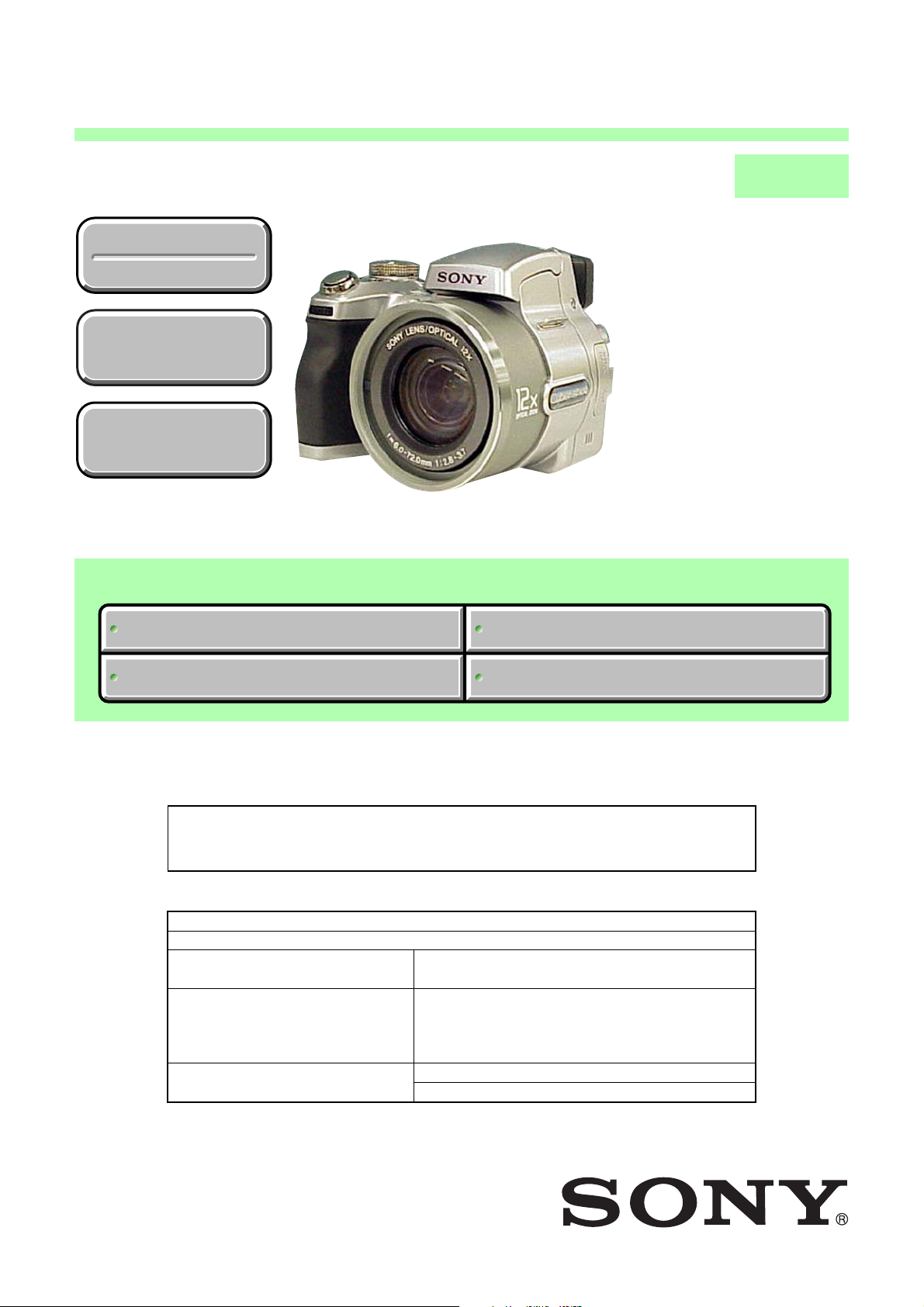
DSC-H1
SERVICE MANUAL
Ver 1.1 2005. 09
Revision History
Revision History
How to use
How to use
Acrobat Reader
Acrobat Reader
Internal memory
Internal memory
ON BOARD
ON BOARD
Link
Link
FRAME SCHEMATIC DIAGRAMS
FRAME SCHEMATIC DIAGRAMS
PRINTED WIRING BOARDS
PRINTED WIRING BOARDS
LEVEL 3
DSC-H1
US Model
Canadian Model
AEP Model
UK Model
E Model
Hong Kong Model
Australian Model
Chinese Model
Japanese Model
Korea Model
Tourist Model
SCHEMATIC DIAGRAMS REPAIR PARTS LIST
SCHEMATIC DIAGRAMS REPAIR PARTS LIST
• For ADJUSTMENTS (SECTION 6), refer to SERVICE MANUAL, ADJ (9-876-880-51).
• For INSTRUCTION MANUAL, refer to SERVICE MANUAL, LEVEL 1 (9-876-880-41).
• Reference number search on printed wiring boards is available.
The information that is not described in this Service Manual is described
in the LEVEL 2 Service Manual.
When repairing, use this manual together with LEVEL 2 Service Manual.
Contents of LEVEL 2 Service Manual
1. SERVICE NOTE
2. DISASSEMBLY
3. BLOCK DIAGRAMS
4. PRINTED WIRING BOARDS AND
SCHEMATIC DIAGRAMS
5. REPAIR PARTS LIST
OVERALL
POWER
CD-576, EV-016, MS-275, PL-039, ST-123, ST-124,
SW-447 BOARD
AF-102, FP-224, MS-029, ST-001, SW-006
FLEXIBLE BOARD
CONTROL SWITCH BLOCK (SW51780)
EXPLODED VIEWS
ELECTRICAL PARTS LIST
DSC-H1
9-876-880-11
Sony EMCS Co.
DIGITAL STILL CAMERA
2005I1600-1
©2005.09
Published by DI Technical Support Department
Page 2
SAFETY CHECK-OUT
After correcting the original service problem, perform the following
safety checks before releasing the set to the customer.
1. Check the area of your repair for unsoldered or poorly-soldered
connections. Check the entire board surface for solder splashes
and bridges.
2. Check the interboard wiring to ensure that no wires are
"pinched" or contact high-wattage resistors.
3. Look for unauthorized replacement parts, particularly
transistors, that were installed during a previous repair . Point
them out to the customer and recommend their replacement.
4. Look for parts which, through functioning, show obvious signs
of deterioration. Point them out to the customer and
recommend their replacement.
5. Check the B+ voltage to see it is at the values specified.
6. Flexible Circuit Board Repairing
• Keep the temperature of the soldering iron around 270˚C
during repairing.
• Do not touch the soldering iron on the same conductor of the
circuit board (within 3 times).
• Be careful not to apply force on the conductor when soldering
or unsoldering.
SAFETY-RELATED COMPONENT WARNING!!
COMPONENTS IDENTIFIED BY MARK 0 OR DOTTED LINE WITH
MARK 0 ON THE SCHEMATIC DIAGRAMS AND IN THE PARTS
LIST ARE CRITICAL TO SAFE OPERATION. REPLACE THESE
COMPONENTS WITH SONY PARTS WHOSE PART NUMBERS
APPEAR AS SHOWN IN THIS MANUAL OR IN SUPPLEMENTS
PUBLISHED BY SONY .
Unleaded solder
Boards requiring use of unleaded solder are printed with the leadfree mark (LF) indicating the solder contains no lead.
(Caution: Some printed circuit boards may not come printed with
the lead free mark due to their particular size.)
: LEAD FREE MARK
Unleaded solder has the following characteristics.
• Unleaded solder melts at a temperature about 40°C higher than
ordinary solder.
Ordinary soldering irons can be used but the iron tip has to be
applied to the solder joint for a slightly longer time.
Soldering irons using a temperature regulator should be set to
about 350°C.
Caution: The printed pattern (copper foil) may peel away if the
heated tip is applied for too long, so be careful!
• Strong viscosity
Unleaded solder is more viscous (sticky , less prone to flow) than
ordinary solder so use caution not to let solder bridges occur such
as on IC pins, etc.
• Usable with ordinary solder
It is best to use only unleaded solder but unleaded solder may
also be added to ordinary solder.
ATTENTION AU COMPOSANT AYANT RAPPORT
À LA SÉCURITÉ!
LES COMPOSANTS IDENTIFÉS P AR UNE MARQUE 0 SUR LES
DIAGRAMMES SCHÉMA TIQUES ET LA LISTE DES PIÈCES SONT
CRITIQUES POUR LA SÉCURITÉ DE FONCTIONNEMENT. NE
REMPLACER CES COMPOSANTS QUE PAR DES PIÈSES SONY
DONT LES NUMÉROS SONT DONNÉS DANS CE MANUEL OU
DANS LES SUPPÉMENTS PUBLIÉS PAR SONY.
CAUTION :
Danger of explosion if battery is incorrectly replaced.
Replace only with the same or equivalent type.
DSC-H1
— 2 —
Page 3

TABLE OF CONTENTS
4. PRINTED WIRING BOARDS AND
SCHEMATIC DIAGRAMS
4-1. FRAME SCHEMATIC DIAGRAM································4-1
4-2. SCHEMATIC DIAGRAMS
• CH-169 (CCD SIGNAL PROCESS)
SCHEMATIC DIAGRAM ····························4-21
• SY-127 (1/11) (LENS DRIVE)
SCHEMATIC DIAGRAM ····························4-23
• SY-127 (2/11) (CAMERA A/D CONV., TIMING
GENERATOR)
SCHEMATIC DIAGRAM ····························4-25
• SY-127 (3/11) (CAMERA DSP., SYSTEM CONTROL)
SCHEMATIC DIAGRAM ····························4-27
• SY-127 (4/11) (256Mbit SDRAM, FLASH MEMORY)
SCHEMATIC DIAGRAM ····························4-29
• SY-127 (5/11) (SUPER AND FLASH MEMORY)
SCHEMATIC DIAGRAM ····························4-31
• SY-127 (6/11) (A/V AMP, USB/AV JACK, SP, MIC)
SCHEMATIC DIAGRAM ····························4-33
• SY-127 (7/11) (PANEL DRIVE)
SCHEMATIC DIAGRAM ····························4-35
• SY-127 (8/11) (STEADY SHOT CONTROL)
SCHEMATIC DIAGRAM ····························4-37
• SY-127 (9/11) (LENS SERVO)
SCHEMATIC DIAGRAM ····························4-39
• SY-127 (10/11) (CONNECTOR)
SCHEMATIC DIAGRAM ····························4-41
• SY-127 (11/11) (DC/DC CONVERTER)
SCHEMATIC DIAGRAM ····························4-43
4-3. PRINTED WIRING BOARDS
• SY-127 (LENS DRIVE, CAMERA A/D CONV.,
TIMING GENERATOR, CAMERA DSP., SYSTEM
CONTROL, 256Mbit SDRAM, FLASH MEMORY,
SUPER AND FLASH MEMORY, A/V AMP, USB/AV
JACK, SP, MIC, PANEL DRIVE, STEADY SHOT
CONTROL, LENS SERVO, CONNECTOR, DC/DC
CONVERTER)
PRINTED WIRING BOARD ·······················4-55
• CH-169 (CCD SIGNAL PROCESS)
PRINTED WIRING BOARD ·······················4-59
4-4. WAVEFORMS ······························································4-62
4-5. MOUNTED PARTS LOCATION ·································4-64
5. REPAIR PARTS LIST
5-2. ELECTRICAL PARTS LIST ········································5-14
DSC-H1
— 3 —
Page 4
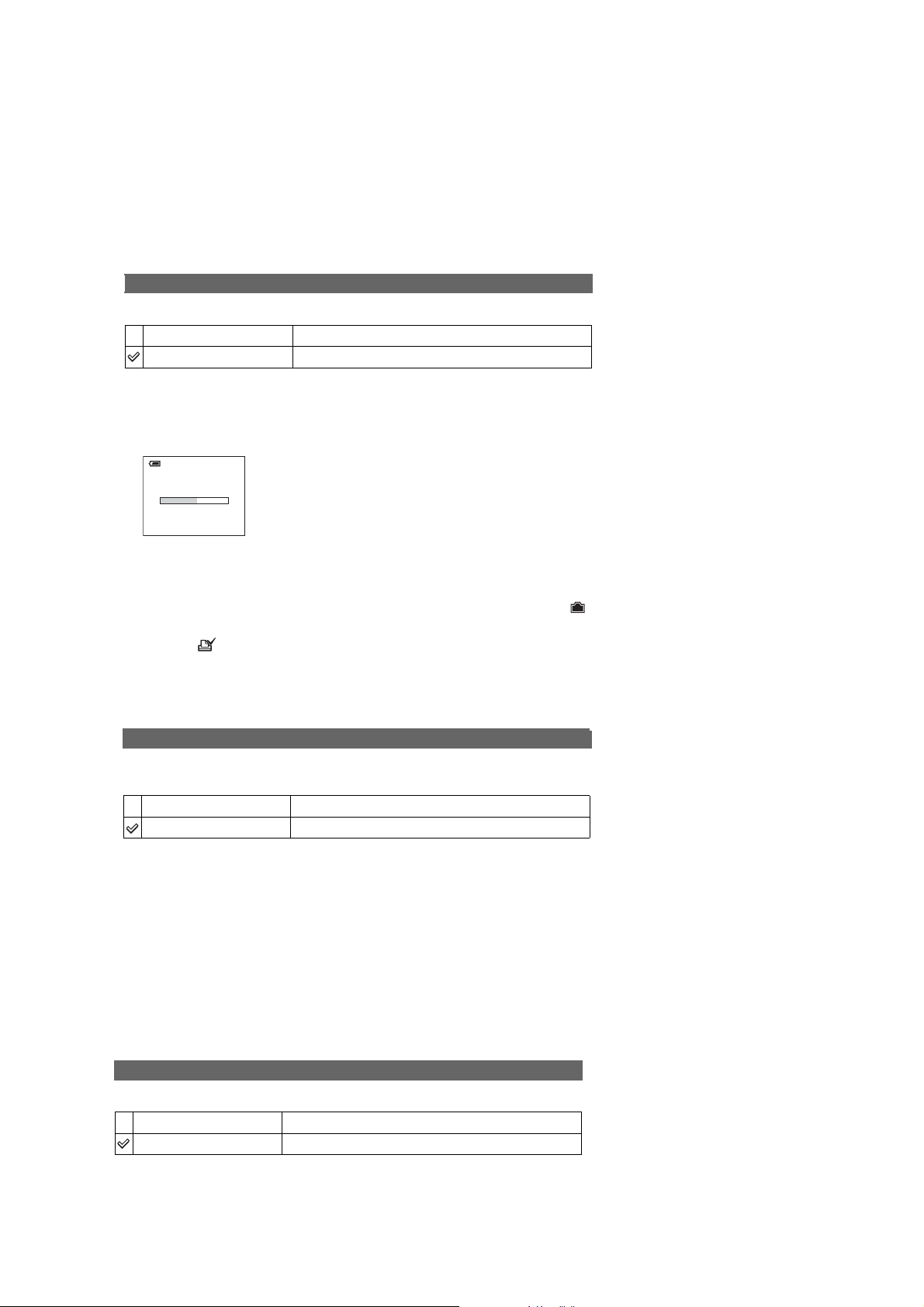
• METHOD FOR COPYING OR ERASING THE DATA IN INTERNAL MEMORY
p
The data can be copied/erased by the operations on the Setup screen. (When erasing the data, execute formatting the internal memory.)
Note: 1 When replacing the SY-127 board, erase the data in internal memory of the board before replacement.
Note: 2 When replacing the SY-127 board or the IC381 on the SY-127 board, execute formatting and initialize the internal memory after
replacement.
Method for Copying the Data in Internal Memory
Copy
Copies all images in the internal memory to a “Memory Stick”.
OK
Cancel
1 Insert a “Memory Stick” having 32 MB or larger capacity.
2 Select [OK] with v on the control button, then press z.
The message “All data in internal memory will be copied Ready?” appears.
3 Select [OK] with v , then press z.
Copying starts.
Copying
102_COPY
Use batteries with enough capacity or the AC Adaptor (not supplied). If you attempt to copy image files
using batteries with little remaining capacity, the batteries may run out, causing copying to fail or possibly
corrupting the data.
You cannot copy individual images.
The original images in the internal memory are retained even after copying. To delete the contents of the
internal memory, remove the “Memory Stick” after copying, then execute the [Format] command in
Internal Memory Tool.
You cannot select a folder copied on a “Memory Stick”.
The setting of (Print order) marks is not copied even when you copy data.
See the following procedure.
Cancels the copying.
Method for Formatting the Internal Memory
Format
Formats the internal memory.
Note that formatting irrevocably erases all data in the internal memory, including even protected images.
OK
Cancel
1 Select [OK] with v on the control button, then press z.
The message “All data in internal memory will be erased Ready?” appears.
2 Select [OK] with v, then press z.
The format is com
lete.
See the following procedure.
Cancels the formatting.
• PROCESS AFTER FIXING FLASH ERROR
When “FLASH error” (Self-diagnosis Code E : 91 : ** ) occurs, to prevent any abnormal situation caused by high voltage, setting of the
flash is changed automatically to disabling charge and flash setting.
After fixing, this setting needs to be deactivated. Flash error code can be initialized by the operations on the Setup screen.
Method for Initializing the Flash Error Code
Initialize
Initializes the setting to the default setting.
OK
Cancel
See the following procedure.
Cancels the resetting.
DSC-H1
1 Select [OK] with v on the control button, then press z.
The message “Initialize all settings Ready?” appears.
2 Select [OK] with v, then press z.
The settings are reset to the default setting.
Make sure that the power is not disconnected during resetting.
— 4 —
Page 5
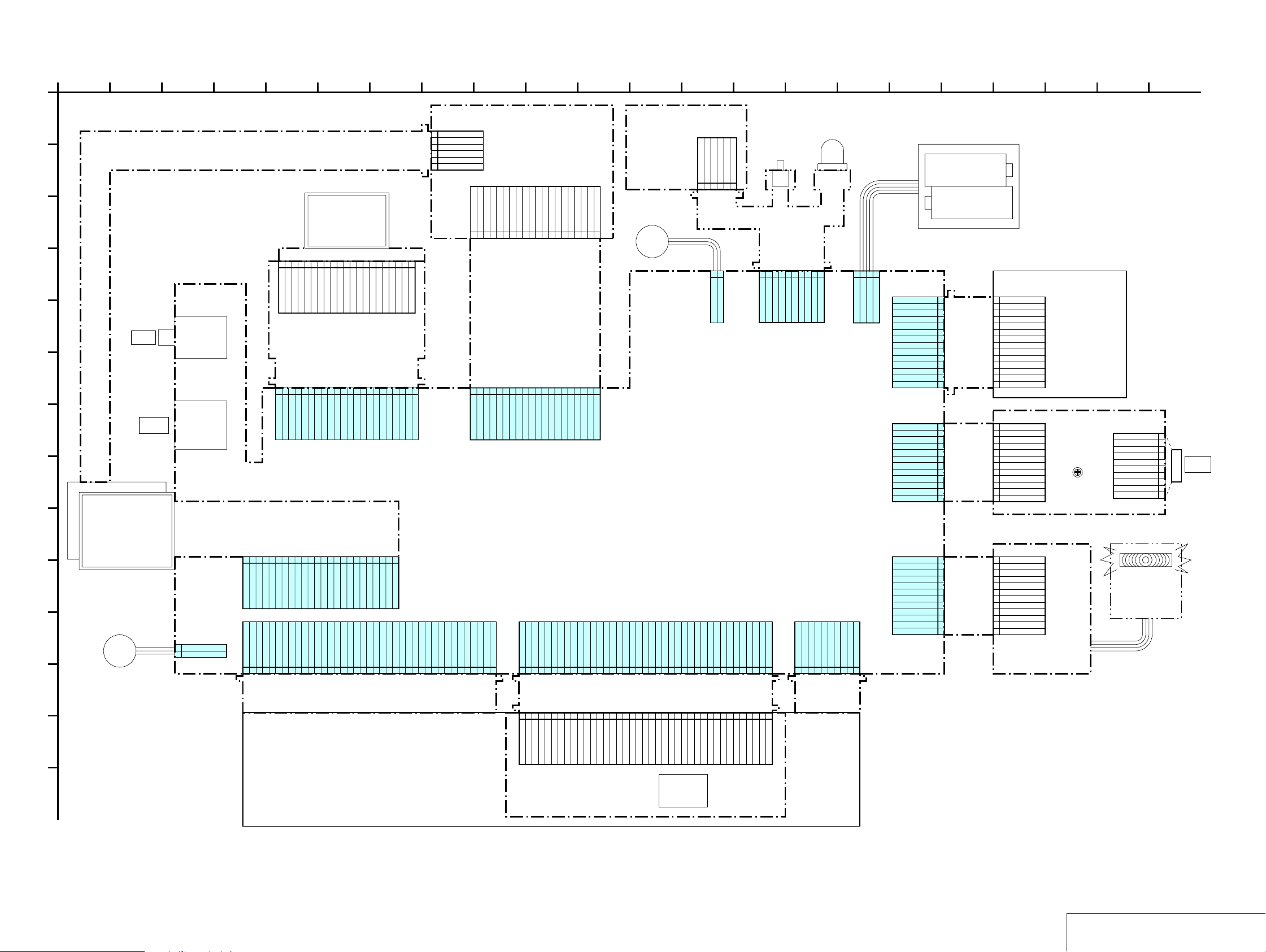
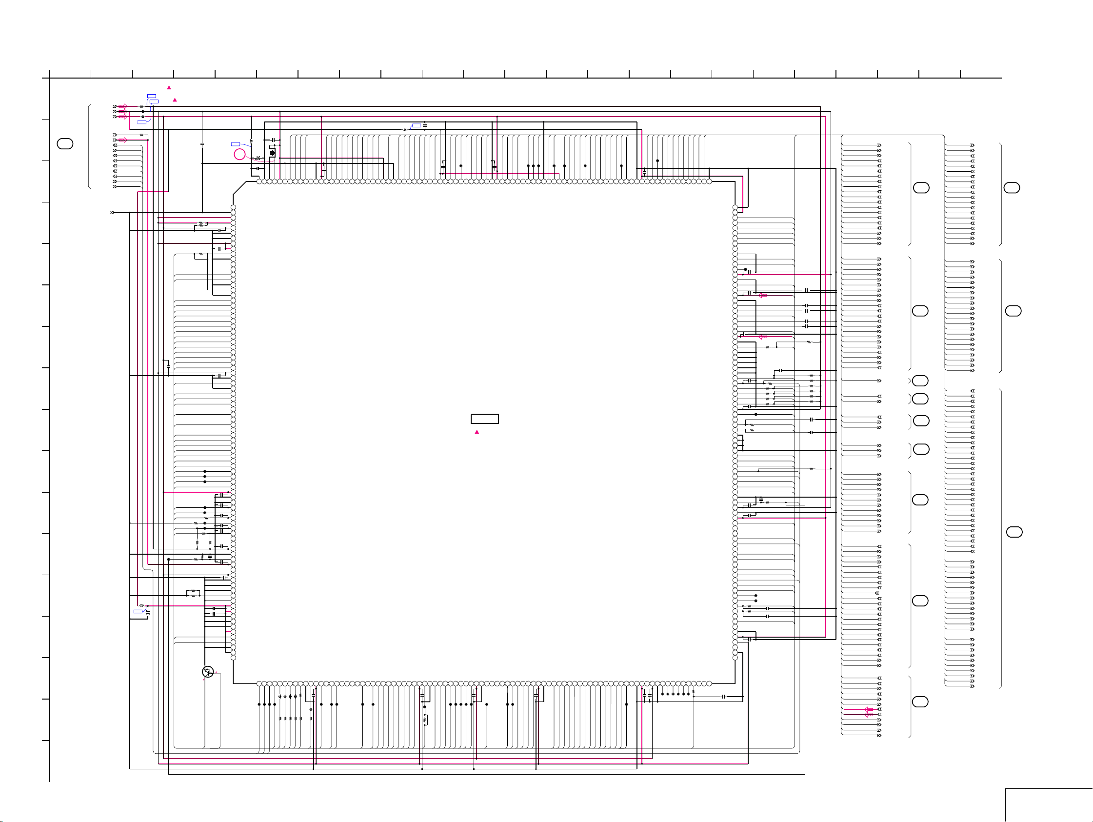
4-1. FRAME SCHEMATIC DIAGRAM
4. PRINTED WIRING BOARDS AND SCHEMATIC DIAGRAMS
Ver 1.1 2005. 09
RGT
DWN
HCK1
73 198
123456789
N.C.
HST
VDD
HCK2
REG_GND
EVF_VSSG
CN452
1 N.C.
2 N.C.
3 N.C.
4 BL_L
5 N.C.
6 BL_H
6P
1
2
6 14 165
A
B
C
21
D
E
AV
COM
PSIG
COLOR EVF UNIT
B
G
R
CS
EV-016 FLEXIBLE BOARD
EVF,BACK LIGHT
1011121314151617181920
EN
REF
VST
VCK
PCG
XSTB
21PCN001
91213
SW-447 BOARD
(1/2) FUNCTION SWITCH
(2/2) PITCH/YAW SENSOR AMP
1 KEY_AD0
2 KEY_AD1
3 D_3.2V
4 REG_GND
5 VST_C_RESET
6 REG_GND
SW-006
FLEXIBLE FLAT CABLE
SY-SW RELAY
104
20P
CN451
7 YAW_AD
8 REG_GND
9 PITCH_AD
10 REG_GND
11 VAP_DD_ON
12 A_3.2V
13 A_3.2V
14 REG_GND
F
ZM_DC_FG_1B
ZM_DC_FG_1A
123456789
XACCESS_LED
XZM_FG_LED
XZM_FG_TR
ZM_FG_VCC
ZM_DC_MOTOR_+
BL_L
BL_L
BL_H
ZM_DC_MOTOR_-
ZM_DC_MOTOR_-
ZM_DC_MOTOR_+
39
1011121314151617181920
BL_H
A_3.2V
A_3.2V
REG_GND
REG_GND
CN513
REG_GND2CSUB3VSUB4RAMDOM_TRIGGER5REG_GND6H2B7REG_GND8H1B9REG_GND10H2A11REG_GND12H1A13REG_GND14CAM_-7.5V_CD15POWER_SAVE16CAM_15V_CD17REG_GND18RG19REG_GND20REG_GND21REG_GND22CCD_OUT23REG_GND24REG_GND25V5A26V1A27V5B28V1B29VHLD30V231V632V3A33V7A34V3B35V7B36VST37V838V439REG_GND
1
VAP_DD_ON
20P
REG_GND
PITCH_AD
REG_GND
YAW_AD
1234567
COM
EVF_BL_L
EVF_BL_H
G
H
I
LCD BACK LIGHT
2.5 INCH
LCD UNIT
USB
123456789
VB
VG
VR
RGT
PSIG
HCK1
TEST2
HCK2
J
9
8
10111213141516171819202122
EN
VB
CS
VG
VR
101112131415161718192021222324
N.C.
TEST1
PCG
PANEL_REF
VST
PSIG
HST
RGT
HCK2
EVF_VSSG
PANEL_REF
PANEL_VDD
22PCN508
24PCN505
EN
N.C.
REG_GND
PANEL_VDD
VCK
DWN
39PCN401
PCG
XSTB_M
PANEL_VSSG
HST
VCK
DWN
HCK1
XSTB_E
REG_GND
CS
VST
COM
SPEAKER
K
CN511
2 SP_-
1 SP_+
2P
IRIS_XB
IRIS_XA
IRIS_B
IRIS_A
SHUTTER_-
SHUTTER_-
123456789
SHUTTER_+
SHUTTER_+
FOCUS_XB
FOCUS_XB
FOCUS_A
FOCUS_A
FOCUS_B
1011121314151617181920212223242526272829303132333435363738
FOCUS_B
FOCUS_XA
FOCUS_XA
REG_GND
LENS_TMP
XFC_RST_LED
XFC_RST_TR
FC_RST_VCC
FC_SENS
ZM_SENS_1ST
XZM_RST_TR1
XZM_RST_LED1
ZM_SENS_2ND
ZM_RST_VCC2
ZM_RST_VCC1
XZM_RST_LED2
XZM_RST_TR2
11 15
REG_GND
15
REG_GND
16 BL_H
17 BL_H
REG_GND
VST_C_RESET
18 BL_L
D_3.2V
19 BL_L
KEY_AD1
20 XACCESS_LED
KEY_AD0
PL-039 BOARD
PLUNGER
MIC
CN301
6P
XSTRB_POPUP
REG_GND
REG_GND
STRB_PLUNGER
REG_GND
STRB_PLUNGER
12345
6
AF-102 FLEXIBLE BOARD
AF LED,LENS COVER SW
1
2
MIC_GND
MIC_SIG
2PCN510
SY-127 BOARD
(1/11) LENS DRIVE
(2/11) CAMERA A/D CONV. TIMING GENERATOR
(3/11) CAMERA DSP,SYSTEM CONTROL
(4/11) 256Mbit SDRAM,FLASH MEMORY
(5/11) SUPER AND FLASH MEMORY
(6/11) A/V AMP,USB/AV JACK,SP,MIC
(7/11) PANEL DRIVE
(8/11) STEADY SHOT CONTROL
(9/11) LENS SERVO
(10/11) CONNECTOR
(11/11) DC/DC CONVERTER
(CH-169 board) CCD SIGNAL PROCESS
CN502
39P
LENS COVER SW
10
REG_GND
REG_GND
STRB_PLUNGER
STRB_PLUNGER
123456789
D_3.2V
XAF_LED
REG_GND
REG_GND
XSTRB_POPUP
XLENS_COVER_SENSE
10PCN507
Y_OUT
P_OUT
A_4.6V
LENS_VC
REG_GND
123456789
AF
10PCN101
P_DRIV_B
P_DRIV_A
Y_DRIV_A
Y_DRIV_B
UNREG
N.C.
10
17
18
BATTERY
123
4
UNREG
REG_GND
REG_GND
4P
CN509
MODE_DIAL0
MODE_DIAL1
KEY_AD2
XAE_LOCK_SW
XSHUTTER_SW
XSHIFT_ON
REG_GND
XPWR_ON
XPWR_LED
XSTRB_LED
REG_GND
REG_GND
REG_GND
ST_UNREG
ST_UNREG
ST_UNREG
REG_GND
STRB_ON
STRB_CHG_CONT
XSTRB_FULL
STRB_CHG
REG_GND
REG_GND
REG_GND
A_3.2V
JOG_A
JOG_B
D_3.2V
MS_VCC
MS_CLK
MS_D3
XMS_IN
MS_D2
MS_D0
MS_D1
MS_BS
VL_3V
CN501
14PCN514
14
13
12
11
10
9
8
7
6
5
4
3
2
1
12PCN506
12
11
10
9
8
7
6
5
4
3
MS-029
FLEXIBLE
2
1
12P
12
11
10
ST_5V
9
8
7
6
5
4
3
ST-001
2
1
CONTROL SWITCH BLOCK
(SW51780)
14P
1
MODE_DIAL0
2
A_3.2V
3
MODE_DIAL1
4
KEY_AD2
5
JOG_A
6
JOG_B
7
XAE_LOCK_SW
XSHUTTER_SW
8
9
XSHIFT_ON
10
REG_GND
11
XPWR_ON
12
XPWR_LED
D_3.2V
13
XSTRB_LED
14
CN251
12P
REG_GND
1
MS_VCC
2
MS_CLK
3
MS_D3
4
XMS_IN
5
MS_D2
6
MS_D0
7
MS_D1
8
MS_BS
9
REG_GND
10
FLAT CABLE
SY-MS RELAY
VL_3V
11
REG_GND
12
CN001
12P
ST_UNREG
1
ST_UNREG
2
ST_UNREG
3
ST_5V
4
REG_GND
5
STRB_ON
6
STRB_CHG_CONT
7
XSTRB_FULL
8
9
STRB_CHG
10
REG_GND
FLEXIBLE
FLAT CABLE
SY-ST RELAY
11
REG_GND
12
REG_GND
ST-123 BOARD
FLASH DRIVE
20
MS-275
BOARD
MEMORY STICK,
LI BATTERY
(LITHIUM BATTERY)
(SECONDARY)
21
10P
VSS
MS_BS
DATA1
SDIO/DATA0
DATA2
INT
DATA3
SCLK
VCC
VSS
10
ST-124
FLEXIBLE BOARD
FLASH
22
1
2
3
CN252
4
MEMORY
5
STICK
CONNECTOR
6
7
8
9
L
M
N
16
DSC-H1
4-1
LENS UNIT
1
2
4
5
CSUB3VSUB
REG_GND
REG_GND
RAMDOM_TRIGGER
CD-576 BOARD
CCD IMAGER
FP-224 FLEXIBLE BOARD
SY-CD RELAY
6
7
8
9
10
11
12
13
14
15
16
17
18RG19
22
23
25
29
30V231V632
H2B
H1B
H2A
H1A
REG_GND
REG_GND
REG_GND
REG_GND
REG_GND
REG_GND20REG_GND21REG_GND
CAM_15V_CD
POWER_SAVE
CAM_-7.5V_CD
39PCN101
CCD_OUT
REG_GND24REG_GND
V5A26V1A27V5B28V1B
VHLD
37V838V439
V3A33V7A34V3B35V7B36VST
REG_GND
CCD IMAGER
4-2
FRAME SCHEMATIC DIAGRAM
Page 6
4-2. SCHEMATIC DIAGRAMS
Link
Link
CH-169 BOARD (CCD SIGNAL PROCESS)
CH-169 BOARD (CCD SIGNAL PROCESS)
SY-127 BOARD (6/11)
SY-127 BOARD (8/11)
(A/V AMP, USB/AV JACK, SP, MIC)
(A/V AMP, USB/AV JACK, SP, MIC)
SY-127 BOARD (1/11) (LENS DRIVE)
SY-127 BOARD (1/11) (LENS DRIVE)
SY-127 BOARD (2/11)
SY-127 BOARD (2/11)
(CAMERA A/D CONV., TIMING GENERATOR)
(CAMERA A/D CONV., TIMING GENERATOR)
SY-127 BOARD (3/11)
SY-127 BOARD (3/11)
(CAMERA DSP., SYSTEM CONTROL)
(CAMERA DSP., SYSTEM CONTROL)
SY-127 BOARD (4/11)
SY-127 BOARD (4/11)
(256Mbit SDRAM, FLASH MEMORY)
(256Mbit SDRAM, FLASH MEMORY)
SY-127 BOARD (5/11)
SY-127 BOARD (5/11)
(SUPER AND FLASH MEMORY)
(SUPER AND FLASH MEMORY)
SY-127 BOARD (7/11) (PANEL DRIVE)
SY-127 BOARD (7/11) (PANEL DRIVE)
SY-127 BOARD (8/11)
SY-127 BOARD (8/11)
(STEADY SHOT CONTROL)
(STEADY SHOT CONTROL)
SY-127 BOARD (9/11) (LENS SERVO)
SY-127 BOARD (9/11) (LENS SERVO)
SY-127 BOARD (10/11) (CONNECTOR)
SY-127 BOARD (10/11) (CONNECTOR)
SY-127 BOARD (11/11) (DC/DC CONVERTER)
SY-127 BOARD (11/11) (DC/DC CONVERTER)
WAVEFORMSCOMMON NOTE FOR SCHEMATIC DIAGRAMS
WAVEFORMSCOMMON NOTE FOR SCHEMATIC DIAGRAMS
DSC-H1
Page 7
4-2. SCHEMATIC DIAGRAMS
4-2. SCHEMATIC DIAGRAMS
THIS NOTE IS COMMON FOR SCHEMATIC DIAGRAMS
(In addition to this, the necessary note is printed in each block)
(For schematic diagrams)
• All capacitors are in µF unless otherwise noted. pF : µ
Link
µF. 50 V or less are not indicated except f or electrolytics
and tantalums.
• Chip resistors are 1/10 W unless otherwise noted.
kΩ=1000 Ω, MΩ=1000 kΩ.
• Caution when replacing chip parts.
New parts must be attached after removal of chip.
Be careful not to heat the minus side of tantalum
capacitor, Because it is damaged by the heat.
• Some chip part will be indicated as follows.
Example C541 L452
22U 10UH
TA A 2520
Kinds of capacitor
Temperature characteristics
External dimensions (mm)
• Constants of resistors, capacitors, ICs and etc with XX
indicate that they are not used.
In such cases, the unused circuits may be indicated.
• Parts with * differ according to the model/destination.
Refer to the mount table for each function.
• All variable and adjustable resistors have characteristic
curve B, unless otherwise noted.
• Signal name
XEDIT→ EDIT PB/XREC → PB/REC
• 2: non flammable resistor
• 5: fusible resistor
• C: panel designation
• A: B+ Line
• B: B– Line
• J : IN/OUT direction of (+,–) B LINE.
• C: adjustment for repair.
• A: VIDEO SIGNAL (ANALOG)
• A: AUDIO SIGNAL (ANALOG)
• A: VIDEO/AUDIO SIGNAL (ANALOG)
• A: VIDEO/AUDIO/SER V O SIGNAL
• A: SERVO SIGNAL
• Circled numbers refer to waveforms.
(Measuring conditions voltage and waveform)
• Voltages and waveforms are measured between the
measurement points and ground when camera shoots
color bar chart of pattern box. They are reference v alues
and reference waveforms.
(VOM of DC 10 MΩ input impedance is used)
• Voltage values change depending upon input
impedance of VOM used.)
1. Connection
Pattern box Color bar chart
Pattern box PTB-450
J-6082-200-A
or
Small pattern box
PTB-1450
J-6082-557-A
Pattern box
100 cm (PTB-450)
40 cm (PTB-1450)
Front of the lens
For PTB-450:
J-6020-250-A
For PTB-1450:
J-6082-559-A
2. Adjust the distance so that the output waveform of
Fig. a and the Fig. b can be obtain.
H
Yellow
Cyan
White
Magenta
Green
AABBA=B
Fig. a (Video output terminal output waveform)
Red
Blue
Electronic beam
scanning frame
CRT picture frame
Precautions Upon Replacing CCD imager
• The CD-576 board mounted as a repair part is not equipped
with a CCD imager.
When replacing this board, remove the CCD imager from
the old one and mount it onto the new one.
• If the CCD imager has been replaced, carry out all the
adjustments for the camera section.
• As the CCD imager may be damaged by static electricity
from its structure, handle it carefully like for the MOS IC.
In addition, ensure that the receiver is not covered with
dusts nor exposed to strong light.
DSC-H1
Fig.b (Picture on monitor TV)
When indicating parts by reference number, please
include the board name.
Note :
The components identified by
mark 0 or dotted line with mark
0 are critical for safety.
Replace only with part number
specified.
Note :
Les composants identifiés par
une marque 0 sont critiques
pour la sécurité.
Ne les remplacer que par une
pièce portant le numéro spécifié.
4-3
Page 8
4-2. SCHEMATIC DIAGRAMS
For Schematic Diagram
• Refer to page 4-55 for printed wiring board.
1
SY-127 BOARD(1/11)
A
LENS DRIVE
XX MARK:NO MOUNT
:Voltage measurement of
the CSP IC and
the Transistors with
mark,is not possible.
B
C
LENS BLOCK is replaced as a block.
So its PRINTED WIRING BOARD and
SCHEMATIC DIAGRAM are omitted.
D
E
F
G
H
I
2
36 119
SHUTTER_-
SHUTTER_-
SHUTTER_+
SHUTTER_+
LENS
UNIT
(1/2)
NOT USE
XFC_RST_LED
XFC_RST_TR
FC_RST_VCC
XZM_RST_TR1
ZM_SENS_1ST
ZM_SENS_2ND
XZM_RST_LED1
ZM_RST_VCC1
ZM_RST_VCC2
XZM_RST_LED2
XZM_RST_TR2
ZM_DC_FG_1B
ZM_DC_FG_1A
ZM_FG_VCC
XZM_FG_LED
XZM_FG_TR
ZM_DC_MOTOR_+
ZM_DC_MOTOR_+
ZM_DC_MOTOR_-
ZM_DC_MOTOR_-
STATIC_GND
IRIS_XB
IRIS_A
IRIS_B
IRIS_XA
FOCUS_XB
FOCUS_XB
FOCUS_A
FOCUS_A
FOCUS_B
FOCUS_B
FOCUS_XA
FOCUS_XA
REG_GND
LENS_TMP
FC_SENS
4
39PCN401
1
2
3
4
5
6
7
8
9
10
11
12
13
14
15
16
17
18
19
20
21
22
23
24
25
26
27
28
29
30
31
32
33
34
35
36
37
38
39
CL401
CL402
5 13
IRIS_XB
IRIS_A
IRIS_B
IRIS_XA
SHUTTER_-
FOCUS_A
FOCUS_B
ZOOM_+
ZOOM_-
STRB_PLUNGER
IRIS_A
IRIS_XA
IRIS_B
IRIS_XB
FOCUS_A
FOCUS_XA
FOCUS_B
FOCUS_XB
ZOOM_+
ZOOM_-
STRB_PLUNGER
SHUTTER_-
SHUTTER_+
E2
D2
B1
D6
E6
B7
C6
B4
B5
B3
A3
F4
F3
R409
22k
±0.5%
OUT1B
OUT2A
OUT2B
OUT3A
OUT3B
OUT4A
OUT4B
OUT5A
OUT5B
OUT6A
OUT6B
OUT7A
OUT7B
R410
22k
±0.5%
C404
XX
XCAM_DR_PS
D4PSF2
OUT1A
SHUTTER_+
FOCUS_XB
FOCUS_XA
2
3
D401
XX
1
87
R411
47k
±0.5%
MSHUT_EN
MSHUT_DIR
STRB_PLUNGER_ON
CL403
CL404
C3
A1
C2
G1
E4
IN6
IN7
EN6
EN7
BR6
IC401
ZOOM/FOCUS/IRIS/SHUTTER
DRIVE
IC401
M63067WG-DF0T
CSP(CHIP SIZE PACKAGE)IC
ZM_BRK_A
C4
B2
BR5
A2
EN5
ZM_DIR_A
A5
IN5
BR4
10
C403
22u
10V
5.0V
C402
0.1u
DIR2A
DIR2B
FC_EN
BRK2B
BRK2A
FC_DIR_A
FC_DIR_B
C5
EN4
IN4
A6
BR3
A7
EN3
B6
IN3
D5
BR2
F1
EN2
E3
IN2
D3
BR1
E5
EN1
G6
IN1
F5
PGND2
E7
PGND2
C7
XCAM_DR_PS
FC_EN
FC_DIR_B
FC_DIR_A
ZM_DIR_A
ZM_BRK_A
STRB_PLUNGER_ON
MSHUT_DIR
MSHUT_EN
BRK2B
BRK2A
DIR2A
DIR2B
12
CL405
D_3.2V
A_3.2V
M_5V
REG_GND
STRB_PLUNGER
LENS_TMP
XFC_RST_LED
FC_SENS
ZM_SENS_1ST
ZM_SENS_2ND
XZM_RST_LED
ZM_DC_FG_1B
ZM_DC_FG_1A
XZM_FG_LED
XCAM_DR_PS
FC_EN
FC_DIR_B
FC_DIR_A
ZM_DIR_A
ZM_BRK_A
STRB_PLUNGER_ON
MSHUT_DIR
MSHUT_EN
BRK2B
BRK2A
DIR2A
DIR2B
@02
@03
@04
(11/11)
(10/11)
(3/11)
J
DSC-H1
VCCF7DGNDF6VREFG7VLIMG3RNFSG4RNFD1VM1D7VM2A4VM3G5VM4C1PGND1E1PGND1
G2
3.2V
C401
16
4-21 4-22
0.1u
10
10
10
R435
R434
R43210R433
SY-127(1/11)
Page 9
For Schematic Diagram
• Refer to page 4-55 for printed wiring board. • Refer to page 4-62 for Wa veforms.
1
25
SY-127 BOARD(2/11)
A
B
C
D
(PAGE 4-16
OF LEVEL2)
E
F
CAMERA A/D CONV.TIMING GENERATOR
XX MARK:NO MOUNT
:Voltage measurement of
the CSP IC and
the Transistors with
mark,is not possible.
CN502
39P
TO
FP-224
FLEXIBLE BOARD
REG_GND
REG_GND
REG_GND
REG_GND
REG_GND
REG_GND
REG_GND
CAM_15V_CD
POWER_SAVE
CAM_-7.5V_CD
REG_GND
REG_GND
REG_GND
REG_GND
REG_GND
RAMDOM_TRIGGER
REG_GND
VHLD
CCD_OUT
VSUB
CSUB
39
38
V4
V8
37
VST
36
35
V7B
34
V3B
33
V7A
32
V3A
31
V6
30
V2
29
28
V1B
27
V5B
26
V1A
25
V5A
24
23
22
21
20
19
18
RG
17
16
15
14
13
12
H1A
11
10
H2A
9
8
H1B
7
6
H2B
5
4
3
2
1
V4
V8
VST
V7B
V3B
V7A
V3A
V6
V2
V1B
V5B
V1A
V5A
RG
H1A
H2A
H1B
H2B
G
H
16
4369
NO MARK:REC/PB MODE
R :REC MODE
P :PB MODE
CA_AD00
CA_AD01
CA_AD02
CA_AD03
CA_AD04
CA_AD05
CA_AD06
CA_AD07
CA_AD08
CA_AD09
CA_AD10
CA_AD11
CA_AD12
CA_AD13
R205
0
R231
C218
10u
10V
C201
0.1u
50V
ATA
3300
R232
2700
R11.3
P0
2
0
Q201
RN1904FE(TPLR3)
R219
10
1/16W
D201
MA2S111-(K8).SO
C202
R204
1u
100k
35V
BJ
6
1
VSUB
R11.3
P0
3
5
VSUB_CONT_POST
0
4
VSUB_CONT_PRE
L201
100uH
C203
3.3u
35V
B
TA
7
V10(VHLD)
20
SUSCK(SUB)
21
D0
22
D1
23
D2
24
D3
25
D4
26
D5
27
D6
28
D7
29
D8
30
D9
31
D10
32
D11
33
D12
34
D13
35
SYNC(*ID)
36
MSHUT(*WEN)
37
C204
0.1u
VST
38
(VST)V9
XFE_CS)
*
STROB(
8
V8
V7A
V7B
15V616
18V819
V7A17V7B
V3B
V5A
V5B
12V413
V5A14V5B
V4
V6
CP201
A/D CONV.S/H,TIMING GENERATOR
CP201
(CH-169 BOARD)
CH-169 BOARD
(PAGE 4-43)
*
Note:The pin number of CP201 on SY-127 board
corresponds to the number from CL001 to
CL074 on CH-169 board.
Note:CP201(CH-169 board)is included in
SY-127 complete board.
CLPOB)
*
CLPDM)
SL(XTG_CS)40XCAM_SSI41XCAM_SCK42XCAM_RESET43VSUB(
39
SAN1_SO
XCS_FE
XSAN1_SCK
*
NC(
44
CL202
R206
0
XSAN_RST_OUT
-7.6V
CA_HR46CA_VR47TG_CKI48MCK49CAM_-7.5V50VM51CAM_15V52TG3V53FE3V54HVDD55HVDD56DRV3V
45
Cl204
CL203
CA_HD
CA_FD
C211
22u
16V
B
TA
R229
100k
2
V3A
V3A11V3B
CLKTGO
FB203
0uH
10 12 13
RG
H1B
H2B
H2A
H1A
12
12
22
R214
C205
0.1u
0uH
0
V2
V1A
V1B
R213
FB209
5RG6
7
9V210
V1A8V1B
CCD_OUT
XX
C213
L202
10uH
FB204
0uH
12
12
R217
R220
R222
R215
0uH
0uH
0uH
0uH
FB207
FB205
FB206
FB208
1
2
3
4
(H1A)H1
(H1B)H3
(H2A)H2
(H2B)H4
C214
XX
2.9V 3.2V
C206
3.3u
35V
B
TA
15.1V
DRVSS
RGVDD
(GND)HL
(*DLLSL)NC
(AVSA)TCVSS
(AVDA)TCVDD
3.2V
1
3.2V
C215
XX
FB202
0uH
GND
GND
GND
GND
GND
GND
GND
GND
GND
GND
GND
GND
FL251
3
74
73
72
71
70
69
68
67
66
65
64
63
62
61
60
59
58
57
0uH
2
4
L203
10uH
C217
L204
10uH
C216
11
CA_AD00
CA_AD01
CA_AD02
CA_AD03
CA_AD04
CA_AD05
CA_AD06
CA_AD07
XX
XX
L206
XX
C207
XX
C208
47u
6.3V
C209
47u
6.3V
C210
47u
6.3V
CA_AD08
CA_AD09
CA_AD10
CA_AD11
CA_AD12
CA_AD13
CA_HD
CA_FD
XCS_FE
CLKTGO
VSUB_CONT_POST
VSUB_CONT_PRE
SAN1_SO
XSAN1_SCK
XSAN_RST_OUT
2.9V
CA_AD00
CA_AD01
CA_AD02
CA_AD03
CA_AD04
CA_AD05
CA_AD06
CA_AD07
CA_AD08
CA_AD09
CA_AD10
CA_AD11
CA_AD12
CA_AD13
CA_HD
CA_FD
XCS_FE
CLKTGO
VSUB_CONT_POST
VSUB_CONT_PRE
SAN1_SO
XSAN1_SCK
XSAN_RST_OUT
CAM_2.9V
D_3.2V
CAM_15V
CAM_-7.5V
REG_GND
@05
@06
@07
@08
(3/11)
(3/11,6/11
7/11,8/11)
(3/11,4/11
5/11,7/11)
(11/11)
DSC-H1
4-23 4-24
SY-127(2/11)
Page 10
For Schematic Diagram
• Refer to page 4-55 for printed wiring board. • Refer to page 4-62 for Waveforms.
Ver 1.1 2005. 09
1
SY-127 BOARD(3/11)
CAMERA DSP,SYSTEM CONTROL
XX MARK:NO MOUNT
A
B
@09
(11/11)
C
D
E
F
G
H
I
J
K
L
M
N
O
P
EVER_3.1V
EVER_2.8V
XSAN0_SCK
SAN0_SO
XPWR_OFF
-7.5V_ON
MS_PWR_ON
BATT_SENS
XDD_RST_OUT
REG_GND
SAN0_SI
XCS_DD
42 1813
:Voltage measurement of
the CSP IC and
3.2V
the Transistors with
mark,is not possible.
3.2V
R301
XSAN0_SCK
SAN0_SI
SAN0_SO
XPWR_OFF
XCS_DD
-7.5V_ON
MS_PWR_ON
BATT_SENS
XDD_RST_OUT
0
0uH
FB301
FB302
0uH
1.2V
XXR302
0
R315
R314
XX
XXR337
CLKTGO
CA_HD
CA_FD
CA_AD00
CA_AD01
CA_AD02
CA_AD03
CA_AD04
CA_AD05
CA_AD06
CA_AD07
CA_AD08
CA_AD09
CA_AD10
CA_AD11
C302
XX
CA_AD12
CA_AD13
NTVDO
FC_DIR_A
FC_DIR_B
FC_EN
ZM_DIR_A
ZM_BRK_A
DIR2A
DIR2B
BRK2A
BRK2B
MSHUT_EN
STRB_ON
VSUB_CONT_POST
XSAN1_SCK
SAN1_SI
SAN1_SO
SCSO
FC_SENS
ZM_SENS_2ND
ZM_SENS_1ST
XXR304
ZM_DC_FG_1A
ZM_DC_FG_1B
R344
0
R325
R326
1kΩ
1kΩ
CL309
XDD_RST_OUT
R311
R313
470k
47k
R345
XX
USB_DPP
USB_DMM
Q301
DTC144EMT2L
SWITCH
R303
680
±0.5%
3
1
0
SCSO
L301
10uH
3.2V
C301
22u
6.3V
TA
A_3.2V
D_3.2V
D_1.2V
5
763 229
10
NO MARK:REC/PB MODE
C319
L303
3.2V
10u
10uH
DSP_DQ16
A10
DQ16
D11
AE11
CPU_D11
DSP_DQ17
D10
DQ17
D10
AB12D9AC11D8AF8
CPU_D10
DSP_DQ18
E11
DQ18
CPU_D09
DSP_DQ19
CPU_D08
6.3V
DSP_DQ23
DSP_DQ22
DSP_DQ21
DSP_DQ20
D26
E12
B11
A11
B10
DQ23
DQ22
DQ21
DQ20
DQ19
VDDQ
CKO
VSSQ
AF9
AF10
AC12D7AA12D6AE12D5AF12D4AF13D3AE13D2AA13D1AB13D0AF14
C318
0.1u B
CL339
XX
R318
CPU_D07
SAN_27M_CLKO
0.1u B
C320
E26
VDDQ(SDRAM)
CPU_D06
CPU_D05
DSP_DQ24
D12
D11
DQ24
VSSQ(SDRAM)
CL345
CPU_D04
DSP_DQ25
CL325
F12
DQ25
CL344
CPU_D03
DSP_DQ28
DSP_DQ26
DSP_DQ30
DSP_DQ29
DSP_DQ27
D14
D13
E13
A12
B12
DQ30
DQ29
DQ28
DQ27
DQ26
IC301
CAMERA DSP,SYSTEM CONTROL
IC301
CXD3188AGG-T6
CSP(CHIP SIZE PACKAGE)IC
VDD
VSS
AF15
AE14
CL343
CL342
CL338
B
C321
0.1u
CPU_D02
CPU_D01
CPU_D00
DSP_DQ31
DQ31
A25
AA14
CL346
CPU_A25
XDSP_QCS0
CL324
D15
AF17
CPU_A17
XQCS0
A17
XDSP_QCAS
CL323
B16
QCAS
A16
AE17
CPU_A16
XDSP_QRAS
CL322
B17
AF16
E25
QRAS
VDDQ
AE15
DSP_QCLKE
A17
QCLKE
VSSQ(SDRAM)
VSSQ
AB17NCAB15
B
C323
0.1u
DSP_QCLK
CL321
A18
CPU_A15
QCLK
A15
D25
VDDQ(SDRAM)
A14
AC17
CPU_A14
CL320
F15
AC18
XDSP_QWE
D17
QWE
A13
AA15
CPU_A13
AQ0
A12
CPU_A12
D18
AE18
CPU_A11
DSP_DQM3
DSP_DQM2
DSP_DQM1
DSP_DQM0
B
C322
0.1u
E15
E14
F14
B15
F13
A16
A15
VSS
VDD
DQM3
DQM2
DQM1
DQM0
XQCS1
A24
A23
A22
A21
A20
A19
A18
AC14
AC13
AC15
AC16
AB14
AE16
CL312
CL311
CPU_A21
CPU_A20
CPU_A19
CPU_A18
DSP_AQ01
DSP_AQ00
C314
0.1u
C315
0.1u
B
L302
10uH
1.2V
3
NC
A1
MD0
B2
MD1
C2
MD2
D2
C303
B
0.1u
VDD
B1
CLKTGEXT
C1
VSS
D1
VDDQ
G2
VDDQ(PLLTGO)
G1
CLKTGO
E1
C304
0.1u
B
VSSQ(PLLTGO)
F1
OPBCLP
F5
DUMCLP
G5
CCDHD
H5
CCDFD
J5
VSS
A2
CLKTGI
F2
VSSQ
E2
ADIN0
K5
ADIN1
G4
ADIN2
H4
ADIN3
L5
ADIN4
H2
ADIN5
H1
ADIN6
J1
ADIN7
J2
ADIN8
M5
ADIN9
J4
ADIN10
K4
ADIN11
M6
ADIN12
K2
ADIN13
K1
C305
0.1u
B
VDDQ
L1
CLKADI
M1
NTVDI
N1
VSSQ
P1
DIR0A
L2
DIR0B
N5
BRK0A
L4
BRK0B
M4
DIR1A
N6
DIR1B
M2
BRK1A
N2
BRK1B
P5
DIR2A
N4
DIR2B
P4
BRK2A
P6
BRK2B
R2
MSHUT_EN
R5
STRBON
R4
VSUBCONT(POST)
T4
CL326
CL327
CL328
CL314
CL315
R342
CL313
CL316
C346
XX
0.1u
0.1u
SCK1
R6
RXD1
T2
TXD1
U2
SCS0
T5
C306
0.1u
B
VDD
R1
VSS
P2
C341
2200p
B
AVSS(SENS)
U1
SENS0
U4
C344
2200p
B
SENS1A
V4
0
SENS1B
U5
C349
XX
SENS2
W2
FG1A
V5
FG1B
W4
C350
XX
NC
W5
C307
0.1u
B
NC
Y2
AVDD(SENS)
T1
VSSBK(SRAM)
V2
C308
0.1u
B
RSTA
Y4
VDDBK(SRAM)
V1
ID
AA2
C309
B
0.1u
VDD(PHY)
W1
VSS(PHY)
AB1
VSS(PHY)
AB2
VBUS
AA4
RREF
Y1
AGND3(PHY)
AD2
C310
B
AVDD3(PHY)
AF2
DVDD1(PHY)
AA1
DGND1(PHY)
AC2
C311
B
VSS(PHY)
AB4
AGND1(PHY)
AE2
AVDD1(PHY)
AF3
DP
AC1
DM
AD1
AGND2(PHY)
AE1
AVDD2(PHY)
AE3
NC
AF1
3.2
2
SAN_USB_VBUS
B
LCD_D3
LCD_D4
LCD_D5
LCD_D6
C312
1
4
22u
6.3V
A
C313
0.1u
B
A4
A3
AVDD(PLL)
SCK0
Y5
AA5
CL329
CL330
XSAN0_SCK
SAN0_SI
X301 12MHz
AVSS(PLL)
RXDO
AB5
A7
VSSQ
TXD0
CL337
SAN0_SO
2
A6
AF4
3
A5
VDDQ
EXTAL
RST_OUT
MSDATA0
AC4
AE4
0uHFB304
CL332
100
R305
XSAN_RST_OUT
MS_D0
B6
0uHFB305
100
R306
MS_D1
XZM_RST_LED
VSSQ(LED)
MSDATA1
AE5
0uH
FB306
100
R307
MS_D2
XFC_RST_LED
MSDATA2
AC5
0uHFB307
100R308
MS_D3
MSDATA3
XZM_FG_LED
MSBS
AB6
0
R356
100
R328
R309
MS_BS
XACCESS_LED
F4
VSSQ
AF5
AF6
C316
0uH
FB309
82
B
0.1u
MS_CLK
LED4E4LED3D4LED2E5LED1B3LED0
MSSCLK
LCD_D7
B
C317
0.1u
A9
B7
VSS
VDD
VDDQ
CS4
CS3
CS0
WE1
WE0
AC6
CL310
XCPU_CS4
CAS
AB7
AE6
AB8
AC7
AB9
CL334
CL333
XCPU_CS0
XCPU_WE1
AF7
AE8
LCD_D2
NTVDO
LCD_D0
LCD_D1
RAS
CKE
AE7
D8
AE9RDAC9
LCDD0D7LCDD1E8LCDD2E7LCDD3D6LCDD4D5LCDD5E6LCDD6B4LCDD7
CL335
XCPU_RD
LCD_CK
LCD_VD
LCD_HD
E10
A8
D9
B5
B9
B8
E9
VSSQ
VDDQ
LCDCK
LCDVD
NTVDO
LCDHD
RDXWR
D15
D14
D13
D12
AC8BSAB10
AC10
AB11
AE10
AF11
CL336
XCPU_BS
CPU_D15
CPU_D14
CPU_D13
CPU_D12
14
DSP_AQ09
DSP_AQ08
DSP_AQ07
DSP_AQ06
DSP_AQ05
DSP_AQ04
DSP_AQ02
DSP_AQ03
CL319
B18
D16
AQ2
AQ1
A11
A10
AF18
AF19A9AE19A8AB16A7AC19A6AB19A5AB18A4AE20A3AF20A2AF21A1AE21A0AF24
CPU_A10
CPU_A09
E17
E19
D19
E16
B19
A19
AQ8
AQ7
AQ6
AQ5
AQ4
AQ3
CPU_A08
CPU_A07
CPU_A06
CPU_A05
CPU_A04
CPU_A03
AQ9
DSP_AQ10
CL318
B20
CPU_A02
16
DSP_AQ11
B13
B14
E18
A20
AQ12
AQ11
AQ10
VSSQ(SDRAM)
VSSQ
AF25
CL331
CPU_A01
DSP_QBA0
0.1u B
C324
A21
B21
QBA0
VDDQ(SDRAM)
VDDQ
XWAIT
AC20
AF22
B
C325
C326
0.1u
DSP_QBA1
QBA1
VDD
B
0.1u
DSP_DQ00
CL317
D21
AF23
DQ0
VSS
DSP_DQ01
D22
AB20
CL303
DQ1
TDI
DSP_DQ02
D20
AE22
CL304
DQ2
TMS
DSP_DQ03
B22
AE23
CL305
DQ3
RTCK
DSP_DQ04
A22
AE25
CL306
DQ4
TDO
DSP_DQ05
A23
AC21
CL307
DQ5
TRST
AB21
DSP_DQ08
DSP_DQ06
DSP_DQ07
E21
E20
B23
DQ7
DQ6
VSUBCONT(PRE) PJ[3](PORT19)
TCK
TO2
AB22
AD25
R346
10k
CL308
STRB_CHG_CONT
DSP_DQ09
E23
B24
VSS
DQ9
DQ8
VSSQ(SDRAM)
VDDQ(SDRAM)
VDDDQ(LED)
AVSSQ(VIDEO)
AVDDQ(VIDEO)
PJ[2](PORT18)
PJ[1](PORT17)
PJ[0](PORT16)
DACK/PI[3](PORT15)
DREQ/PI[2](PORT14)
PI[1](PORT13)
PI[0](PORT12)
PH[3](PORT11)
PH[2](PORT10)
PH[1](PORT9)
PH[0](PORT8)
PG[7](PORT7)
PG[6](PORT6)
PG[5}(PORT5)
PG[4](PORT4)
PG[3](PORT3)
PG[2](PORT2)
PG[1](PORT1)
PG[0](PORT0)
TO1
TO0
NC
AC25
AF26
AVSSQ(LED)
AVSSQ(AU)
AVDDQ(AU)
AVSS(AD)
AVDD(AD)
TRACECLK
17
A14
A13
DQ10
A24
DQ11
A25
DQ12
B25
DQ13
C25
DQ14
C26
DQ15
B26
NC
A26
F23
LED5
E22
LED6
D23
CL347
LED7
F22
F26
C327
0.1u
M25
VOUT
H26
VREF
J26
G26
C328
0.1u
N26
VRP
H23
VRN
G22
AOUT
K26
VRL
G23
VRH
H22
AIN
L26
M26
C329
0.1u
B
N25
AN[11]
G25
AN[10]
H25
AN[9]
J22
AN[8]
F25
AN[7]
J23
AN[6]
K22
C330
0.1u
AN[5]
J25
AN[4]
K25
AN[3]
L23
AN[2]
K23
AN[1]
L25
AN[0]
L22
P26
0.1u BC331
INT3
M21
INT2
P22
R338
INT1
N21
R339
INT0
P23
TEST3
M23
TEST2
N22
TEST1
M22
TEST0
N23
R23
P21
R25
T25
P25
T23
U23
R22
VSSQ
U26
C332
0.1u
RST
R26
VDDQ
T26
VSS
V26
VDD
W26
U25
C333
0.1u
V25
R21
V23
W23
T22
W25
Y26
Y25
U22
Y23
AA23
CTS4
V22
RTS4
AA25
TXD4
AA26
RXD4
AB25
TI3B
W22
TI3A
AB23
R350
TO3
AC22
TI2B
AC23
TI2A
Y22
VSS
C334
AC26
0.1u B
VDD
AB26
VDDQ
AE26
AE24
VSSQ
AD26
NC
AA22
C345
0.1u
B
B
B
B
CL340
10k
10k
B
B
CL301
CL302
10kR348
10k
R341
10k
R324
100k
±0.5%
R319
10k
R320
10k
R321
10k
R322
10k
C335
0.1u
R323
2200
STRB_PLUNGER_ON
C343
B0.1u
C399
B
0.1u
XLENS_COVER_SENSE
DSP_DQ10
DSP_DQ11
DSP_DQ12
DSP_DQ13
DSP_DQ14
DSP_DQ15
XSTRB_LED
XPWR_LED
SAN_VOUT
SAN_AUOUT
SAN_AUIN
KEY_AD2
C342
0.1u
B
LENS_TMP
BATT_SENS
KEY_AD1
KEY_AD0
MODE_DIAL1
MODE_DIAL0
CPU_R/XB
XAE_LOCK_SW
XSHUTTER_SW
VSUB_CONT_PRE
XCAM_DR_PS
MSHUT_DIR
MS_PWR_ON
-7.5V_ON
XLINE_MUTE
VIDEO_AMP_ON
STRB_CHG
XDD_RST_OUT
XAV_JACK_IN
XSTRB_FULL
XCS_PANEL
XCS_AUDIO
XCS_IC901
XPWR_OFF
XSTRB_POPUP
AU_3.2V
XCS_DD
VI_3.2V
XCS_FE
JOG_B
JOG_A
C340
0.1u
B
C336
XX
C337
XX
XX
C338
C339
XX
R334
10k
47k
R329
R330
±0.5%
220k
R333
10k
10k
R332
R327
220k
220k
R331
XXC347
C348
XX
XX
R336
20 2315118
CLKTGO
CA_HD
CA_FD
CA_AD00
CA_AD01
CA_AD02
CA_AD03
CA_AD04
CA_AD05
CA_AD06
CA_AD07
CA_AD08
CA_AD09
CA_AD10
CA_AD11
CA_AD12
CA_AD13
VSUB_CONT_POST
VSUB_CONT_PRE
XCS_FE
FC_DIR_A
FC_DIR_B
FC_EN
ZM_DIR_A
ZM_BRK_A
DIR2A
DIR2B
XCAM_DR_PS
MSHUT_EN
ZM_SENS_1ST
ZM_SENS_2ND
ZM_DC_FG_1A
ZM_DC_FG_1B
BRK2B
BRK2A
FC_SENS
XZM_FG_LED
XZM_RST_LED
XFC_RST_LED
STRB_PLUNGER_ON
MSHUT_DIR
LENS_TMP
XSAN_RST_OUT
XSAN1_SCK
SAN1_SO
SAN1_SI
NTVDO
XCS_IC901
CPU_R/XB
CPU_A25
XCPU_CS4
XCS_PANEL
LCD_D0
LCD_D1
LCD_D2
LCD_D3
LCD_D4
LCD_D5
LCD_D6
LCD_D7
LCD_VD
LCD_HD
LCD_CK
XSTRB_FULL
STRB_CHG
STRB_ON
STRB_CHG_CONT
XSTRB_POPUP
XACCESS_LED
KEY_AD0
KEY_AD1
KEY_AD2
XLENS_COVER_SENSE
XSHUTTER_SW
XAE_LOCK_SW
MODE_DIAL0
MODE_DIAL1
XSTRB_LED
XPWR_LED
JOG_A
JOG_B
MS_D0
MS_D1
MS_D2
MS_D3
MS_BS
MS_CLK
SAN_USB_VBUS
XAV_JACK_IN
USB_DPP
SAN_AUIN
SAN_AUOUT
XLINE_MUTE
VI_3.2V
AU_3.2V
XCS_AUDIO
USB_DMM
VIDEO_AMP_ON
SAN_VOUT
2112 19
CLKTGO
CA_HD
CA_FD
CA_AD00
CA_AD01
CA_AD02
CA_AD03
CA_AD04
CA_AD05
CA_AD06
CA_AD07
CA_AD08
CA_AD09
CA_AD10
CA_AD11
CA_AD12
CA_AD13
VSUB_CONT_POST
VSUB_CONT_PRE
XCS_FE
FC_DIR_A
FC_DIR_B
FC_EN
ZM_DIR_A
ZM_BRK_A
DIR2A
DIR2B
XCAM_DR_PS
MSHUT_EN
ZM_SENS_1ST
ZM_SENS_2ND
ZM_DC_FG_1A
ZM_DC_FG_1B
BRK2B
BRK2A
FC_SENS
XZM_FG_LED
XZM_RST_LED
XFC_RST_LED
STRB_PLUNGER_ON
MSHUT_DIR
LENS_TMP
XSAN_RST_OUT
XSAN1_SCK
SAN1_SO
SAN1_SI
NTVDO
XCS_IC901
CPU_R/XB
CPU_A25
XCPU_CS4
XCS_PANEL
LCD_D0
LCD_D1
LCD_D2
LCD_D3
LCD_D4
LCD_D5
LCD_D6
LCD_D7
LCD_VD
LCD_HD
LCD_CK
XSTRB_FULL
STRB_CHG
STRB_ON
STRB_CHG_CONT
XSTRB_POPUP
XACCESS_LED
KEY_AD0
KEY_AD1
KEY_AD2
XLENS_COVER_SENSE
XSHUTTER_SW
XAE_LOCK_SW
MODE_DIAL0
MODE_DIAL1
XSTRB_LED
XPWR_LED
JOG_A
JOG_B
MS_D0
MS_D1
MS_D2
MS_D3
MS_BS
MS_CLK
SAN_USB_VBUS
XAV_JACK_IN
USB_DPP
SAN_AUIN
SAN_AUOUT
XLINE_MUTE
VI_3.2V
AU_3.2V
XCS_AUDIO
USB_DMM
VIDEO_AMP_ON
SAN_VOUT
@05
@04
@07
@06
@10
@11
@12
@13
@14
XCPU_WE1
XCPU_WE1
XCPU_RD
XCPU_RD
CPU_D00
CPU_D00
CPU_D01
CPU_D01
CPU_D02
CPU_D02
CPU_D03
CPU_D03
CPU_D04
CPU_D04
CPU_D05
CPU_D05
CPU_D06
CPU_D07
CPU_D08
CPU_D09
CPU_D10
CPU_D11
CPU_D12
CPU_D13
CPU_D14
CPU_D15
CPU_A20
CPU_A21
CPU_A01
CPU_A02
CPU_A03
CPU_A04
CPU_A05
CPU_A06
CPU_A07
CPU_A08
CPU_A09
CPU_A10
CPU_A11
CPU_A12
CPU_A13
CPU_A14
CPU_A15
CPU_A16
CPU_A17
CPU_A18
CPU_A19
XCPU_CS0
XCPU_BS
SAN_27M_CLKO
DSP_DQ00
DSP_DQ01
DSP_DQ02
DSP_DQ03
DSP_DQ04
DSP_DQ05
DSP_DQ06
DSP_DQ07
DSP_DQ08
DSP_DQ09
DSP_DQ10
DSP_DQ11
DSP_DQ12
DSP_DQ13
DSP_DQ14
DSP_DQ15
DSP_DQ16
DSP_DQ17
DSP_DQ18
DSP_DQ19
DSP_DQ20
DSP_DQ21
DSP_DQ22
DSP_DQ23
DSP_DQ24
DSP_DQ25
DSP_DQ26
DSP_DQ27
DSP_DQ28
DSP_DQ29
DSP_DQ30
DSP_DQ31
DSP_AQ00
DSP_AQ01
DSP_AQ02
DSP_AQ03
DSP_AQ04
DSP_AQ05
DSP_AQ06
DSP_AQ07
DSP_AQ08
DSP_AQ09
DSP_AQ10
DSP_AQ11
DSP_QBA0
DSP_QBA1
DSP_DQM0
DSP_DQM1
DSP_DQM2
DSP_DQM3
XDSP_QCS0
XDSP_QWE
XDSP_QRAS
XDSP_QCAS
DSP_QCLKE
DSP_QCLK
(2/11)
(1/11)
(2/11,
4/11,
5/11,
7/11)
(2/11,
6/11,
7/11,
8/11)
(8/11)
(5/11)
(7/11)
(10/11)
(6/11)
@15
@16
@17
(4/11,
5/11)
(4/11)
(4/11)
Q
16
DSC-H1
4-25 4-26
SY-127(3/11)
Page 11
For Schematic Diagram
• Refer to page 4-55 for printed wiring board.
1
:Voltage measurement of
SY-127 BOARD(4/11)
A
B
C
D
E
F
G
H
256Mbit SDRAM,FLASH MEMORY
XX MARK:NO MOUNT
D_1.8V
D_3.2V
REG_GND
XCPU_CS0
SAN_27M_CLKO
XCPU_BS
CPU_A01
CPU_A02
CPU_A03
CPU_A04
CPU_A05
CPU_A06
CPU_A07
CPU_A08
CPU_A09
CPU_A10
CPU_A11
CPU_A12
CPU_A13
CPU_A14
CPU_A15
CPU_A16
CPU_A17
CPU_A18
CPU_A19
XSAN_RST_OUT
CPU_A20
CPU_A21
XCPU_RD
XCPU_WE1
CPU_D00
CPU_D01
CPU_D02
CPU_D03
CPU_D04
CPU_D05
CPU_D06
CPU_D07
CPU_D08
CPU_D09
CPU_D10
CPU_D11
CPU_D12
CPU_D13
CPU_D14
CPU_D15
@07
@15
@18
@16
(2/11,3/11,
5/11,7/11)
(3/11,5/11)
(11/11)
(3/11)
XCPU_CS0
SAN_27M_CLKO
XCPU_BS
CPU_A01
CPU_A02
CPU_A03
CPU_A04
CPU_A05
CPU_A06
CPU_A07
CPU_A08
CPU_A09
CPU_A10
CPU_A11
CPU_A12
CPU_A13
CPU_A14
CPU_A15
CPU_A16
CPU_A17
CPU_A18
CPU_A19
XSAN_RST_OUT
CPU_A20
CPU_A21
XCPU_RD
XCPU_WE1
CPU_D00
CPU_D01
CPU_D02
CPU_D03
CPU_D04
CPU_D05
CPU_D06
CPU_D07
CPU_D08
CPU_D09
CPU_D10
CPU_D11
CPU_D12
CPU_D13
CPU_D14
CPU_D15
CPU_D10
CPU_D11
CPU_D12
CPU_D13
CPU_D14
CPU_D15
XCPU_BS
SAN_27M_CLKO
XCPU_WE1
XSAN_RST_OUT
XCPU_CS0
XCPU_RD
the CSP IC and
the Transistors with
mark,is not possible.
0uHFB352
FB351
0uH
CL351
R351
0
XXC352
1.8V 3.2V
5
CPU_D09
CPU_D08
CPU_D07
CPU_D06
CPU_D05
CPU_D04
D9
D10
F5
D11
F4
D12
D5
D13
F3
D14
F2
D15
E2
WAIT
D3
XADV
C4
CLK
B4
XWE
C5
XRST
B5
XWP
D6
XCE
E7
XOE
F8
A service for IC351 is not available
because an adjustment is required
before replacement.
A0D8A1C8A2B8A3A8A4B7A5A7A6C7A7A2A8B2A9C2A10A1A11B1A12
E8
CPU_A01
CPU_A02
IC351
FLASH MEMORY
PH28F320W30TD70-A01
CSP(CHIP SIZE PACKAGE)IC
CPU_A03
CPU_A04
CPU_A05
CPU_A06
CPU_D03
IC351
CPU_A07
CPU_D02
CPU_A08
CPU_D01
F7D0E6D1E5D2G5D3E4D4G3D5E3D6G1D7G7D8F6
CPU_A09
CPU_D00
CPU_A10
E1
CPU_A11
VCCQG6VCCQ
CPU_A12
711 16
C351
XX
A4
VCCG4VCC
VPP
A5
NC
D7
VSSQ
G2
VSSQ
G8
VSS
F1
VSS
A3
NC
C3
A20
B3
A19
C6
A18
A6
A17
B6
A16
D4
A15
D1
A14
D2
A13
C1
CPU_A13
CPU_A14
I
8
C353
10u
6.3V
0.1u
0.1u
0.1u
0.1u
C356
C355
C357
C358
CPU_A21
CPU_A20
CPU_A19
CPU_A18
CPU_A17
CPU_A16
CPU_A15
@17
913
DSP_DQ00
DSP_DQ01
DSP_DQ02
DSP_DQ03
DSP_DQ04
DSP_DQ05
DSP_DQ06
DSP_DQ07
DSP_DQ08
DSP_DQ09
DSP_DQ10
DSP_DQ11
DSP_DQ12
DSP_DQ13
DSP_DQ14
DSP_DQ15
DSP_DQ16
DSP_DQ17
DSP_DQ18
DSP_DQ19
DSP_DQ20
DSP_DQ21
DSP_DQ22
DSP_DQ23
DSP_DQ24
DSP_DQ25
(3/11)
DSP_DQ26
DSP_DQ27
DSP_DQ28
DSP_DQ29
DSP_DQ30
DSP_DQ31
DSP_AQ00
DSP_AQ01
DSP_AQ02
DSP_AQ03
DSP_AQ04
DSP_AQ05
DSP_AQ06
DSP_AQ07
DSP_AQ08
DSP_AQ09
DSP_AQ10
DSP_AQ11
DSP_QBA0
DSP_QBA1
XDSP_QCS0
XDSP_QRAS
XDSP_QCAS
XDSP_QWE
DSP_DQM0
DSP_DQM1
DSP_DQM2
DSP_DQM3
DSP_QCLKE
DSP_QCLK
DSP_DQ00
DSP_DQ01
DSP_DQ02
DSP_DQ03
DSP_DQ04
DSP_DQ05
DSP_DQ06
DSP_DQ07
DSP_DQ08
DSP_DQ09
DSP_DQ10
DSP_DQ11
DSP_DQ12
DSP_DQ13
DSP_DQ14
DSP_DQ15
DSP_DQ16
DSP_DQ17
DSP_DQ18
DSP_DQ19
DSP_DQ20
DSP_DQ21
DSP_DQ22
DSP_DQ23
DSP_DQ24
DSP_DQ25
DSP_DQ26
DSP_DQ27
DSP_DQ28
DSP_DQ29
DSP_DQ30
DSP_DQ31
DSP_AQ00
DSP_AQ01
DSP_AQ02
DSP_AQ03
DSP_AQ04
DSP_AQ05
DSP_AQ06
DSP_AQ07
DSP_AQ08
DSP_AQ09
DSP_AQ10
DSP_AQ11
DSP_QBA0
DSP_QBA1
XDSP_QCS0
XDSP_QRAS
XDSP_QCAS
XDSP_QWE
DSP_DQM0
DSP_DQM1
DSP_DQM2
DSP_DQM3
DSP_QCLKE
DSP_QCLK
10 152
L351
3.2V
47uH
C359
10u
6.3V
VSSQ
IC353
IC353
DSP_DQ18
DSP_DQ20
DSP_DQ19
A3
DSP_DQ21
DSP_DQ22
VSSF1VSSL3VSSR3VSS
DSP_AQ00
DSP_AQ01
DSP_AQ02
DSP_AQ03
DSP_AQ04
DSP_AQ05
DSP_AQ06
DSP_AQ07
DSP_AQ08
DSP_AQ09
DSP_AQ10
DSP_QBA0
DSP_QBA1
DSP_DQ00
DSP_DQ01
DSP_DQ02
DSP_DQ03
DSP_DQ04
DSP_DQ05
DSP_DQ06
DSP_DQ07
DSP_DQ08
B3
B8
E9
L9
N1
P3
VSSQ
CSP(CHIP SIZE PACKAGE)IC
DSP_DQ14
DSP_DQ15
DSP_DQ16
DSP_DQ17
VSSQC1VSSQD1VSSQ
256Mbit SDRAM
K4S563233F-HN75T
VSSQM1VSSQ
VSSQP8VSSQ
VSSQ
A0
G8
A1
G9
A2
F7
A3
F3
A4
G1
A5
G2
A6
G3
A7
H1
A8
H2
A9
J3
A10
G7
BA0
J7
BA1
H8
DQ0
R8
DQ1
N7
DQ2
R9
DQ3
N8
DQ4
P9
DQ5
M8
DQ6
M7
DQ7
L8
DQ8
L2
DQ9M2DQ10P1DQ11N2DQ12R1DQ13N3DQ14R2DQ15E8DQ16D7DQ17D8DQ18B9DQ19C8DQ20A9DQ21C7DQ22A8DQ23A2DQ24C3DQ25A1DQ26C2DQ27B1DQ28D2DQ29D3DQ30E2DQ31
M3
DSP_DQ12
DSP_DQ13
DSP_DQ11
DSP_DQ09
DSP_DQ10
C360
0.1u
B
DSP_DQ23
DSP_DQ24
DSP_DQ25
C361
0.1u
B
DSP_DQ26
144 1236
C362
0.1u
DSP_DQ27
DSP_DQ28
B
DSP_DQ29
B7
DSP_DQ30
DSP_DQ31
C363
0.1u
B
VDDQC9VDDQD9VDDQE1VDDQL1VDDQM9VDDQN9VDDQP2VDDQP7VDDQ
VDDQ
B2
VDD
R7
VDD
L7
VDD
F9
VDD
A7
(NC)
K3
(NC)
K2
DSP_AQ11
H9
H7
H3
E7
E3
DSP_QCLK
J1
DSP_QCLKE
J2
XDSP_QCAS
K7
XDSP_QRAS
J9
XDSP_QWE
K8
XDSP_QCS0
J8
DSP_DQM3
F2
DSP_DQM2
F8
DSP_DQM1
K1
DSP_DQM0
K9
CAS#
RAS#
DQM3
DQM2
DQM1
DQM0
A11
(NC)
(NC)
(NC)
(NC)
CLK
CKE
WE#
CS#
DSC-H1
16
4-27 4-28
SY-127 (4/11)
Page 12

For Schematic Diagram
• Refer to page 4-55 for printed wiring board.
A
B
C
D
E
F
1
SY-127 BOARD(5/11)
SUPER AND FLASH MEMORY
XX MARK:NO MOUNT
@19
@15
@11
@07
(11/11)
(3/11.
4/11)
(3/11)
(2/11,
3/11,
4/11,
7/11)
D_3.2V
REG_GND
CPU_A21
CPU_A20
XCPU_WE1
XCPU_RD
CPU_D00
CPU_D01
CPU_D02
CPU_D03
CPU_D04
CPU_D05
CPU_D06
CPU_D07
CPU_D08
CPU_D09
CPU_D10
CPU_D11
CPU_D12
CPU_D13
CPU_D14
CPU_D15
CPU_A25
CPU_R/XB
XCPU_CS4
XSAN_RST_OUT
XSAN_RST_OUT
CPU_A21
CPU_A20
XCPU_WE1
XCPU_RD
CPU_D00
CPU_D01
CPU_D02
CPU_D03
CPU_D04
CPU_D05
CPU_D06
CPU_D07
CPU_D08
CPU_D09
CPU_D10
CPU_D11
CPU_D12
CPU_D13
CPU_D14
CPU_D15
CPU_A25
CPU_R/XB
XCPU_CS4
3
:Voltage measurement of
the CSP IC and
the Transistors with
mark,is not possible.
CPU_D06
CPU_D07
CPU_D14
4
A11
DU
B11
DU
C11
DU
D11
DU
C10
I/O_7
D10
VSS
C9
I/O_8
D9
DU
C8
XMRES
D8
DU
C7
I/O_15
D7
DU
D6
DU
C6
DU
D5
DU
C5
DU
D4
DU
C4
DU
D3
DU
C3
DU
D2
DU
C2
DU
B2
DU
A2
56
3.2V
C381
0.1u
CPU_D12
CPU_D05
CPU_D13
CPU_D15
F11DUE7
E8
E9
E10
E11
B12
A12
DU
DU
DU
DU
I/O_16
I/O_14
I/O_6
I/O_13
F8DUF9DUF10
VCC
IC381
SUPER AND FLASH MEMORY
IC381
HN29V256A0BBP-30
CSP(CHIP SIZE PACKAGE)IC
CPU_D04
G7DUF7
I/O_5
CPU_D10
G8
I/O_11
CPU_D03
G10
G9
I/O_4
CPU_D11
G11
I/O_12
H7
DU
CPU_D08
CPU_D00
H8
I/O_1
H9
I/O_9
CPU_D09
CPU_D01
H10
I/O_2
H11
I/O_10
L12
DU
DU
87
XCE
XRE
VSS
CLE
ALE
DU
M12
DU
M11
DU
L11
DU
K11
DU
J11
K10
DU
J10
K9
DU
J9
K8
DU
J8
DU
K7
DU
J7
DU
J6
DU
K6
DU
J5
DU
K5
DU
J4
DU
K4
J3
K3
DU
J2
DU
K2
DU
L2
XCPU_CS4
XCPU_RD
92
CPU_A21
CPU_A20
G
DSC-H1
16
DUB1DUE2DUE3XWEE4R/XBE5DUE6DUF3VSSF4XRESF5DUF6PREG6I/O_3G5DUG4DUG3XWPG2DUH6DUH5DUH4DUH3DUH2DUL1DUM1DUM2DU
A1
C382
XX
R381
0
XCPU_WE1
CPU_R/XB
XSAN_RST_OUT
CPU_D02
CPU_A25
4-29 4-30
SY-127 (5/11)
Page 13

For Schematic Diagram
• Refer to page 4-55 for printed wiring board.
1
SY-127 BOARD(6/11)
A/V AMP,USB/AV JACK,SP,MIC
A
XX MARK:NO MOUNT
NO MARK:REC/PB MODE
R :REC MODE
P :PB MODE
B
C
D
@20
(11/11)
274
3
:Voltage measurement of
the CSP IC and
the Transistors with
mark,is not possible.
MIC901
MIC UNIT
SP901
SPEAKER
REG_GND
USB_VBUS
MIC_SIG
MIC_GND
D_3.2V
A_3.2V
CN510
CN511
2P
2
1
2P
1SP_+
2SP_-
C802
10u
6.3V
3.2V
C801
0.47u
6.3V
C824
1u
6.3V
L801
10uH
A6
A5
C4
A4
B4
A3
B3
A2
B2
NC
SP+
NC
SPVCC
NC
SPGND
NC
SP-
SPBIAS
5
C809
0.022u
16V
R801
2200
B5
MIC_REG
B6
C806
0.1u
50V
C5
MIC_IN
470k
R803
C6
ALC_IN
PRE_OUT
C803
C804
0.01u
16V
10u
6.3V
IC801
MIC/SPEAKER/AUOUT
AMP
IC801
BH6414GLU-E2
CSP(CHIP SIZE PACKAGE)IC
NCB1BEEPC3NCC1SP_INC2EVR_OUTD1LINE_OUTD2MUTE_Tr_OUTE1MUTEGNDE2AGND
A1
69
C810
1u
6.3V
C821
4700p
16V
R810
C807
8200
0.01u
16V
E6
D4NCD6
D5
TAU
ABIAS
F6
NC
MIC_OUT
LINE_IN
AVCC
XSEN
DVDD
SDATA
xRESET
xLINE_MUTE
SCLK
TEST
C812
0.1u
E5
F5
E4
F4
E3
F3
D3
F2
F1
SAN_VOUT
SAN_USB_VBUS
USB_DPP
USB_DMM
XAV_JACK_IN
VIDEO_AMP_ON
3.2
C813
2.2u
6.3V
L803
10uH
IC803
R1141Q281B-TR-FA
1
Vout
2
GND
Vdd
CE
IC803
3.2V REG
3.2
4
3.2
3
10 118
SAN_AUIN
SAN_VOUT
SAN_USB_VBUS
USB_DPP
USB_DMM
XAV_JACK_IN
VIDEO_AMP_ON
XCS_AUDIO
SAN_AUOUT
(3/11)
(2/11,3/11,
7/11,8/11)
XLINE_MUTE
AU_3.2V
VI_3.2V
XSAN1_SCK
SAN1_SO
@14
@06
E
F
G
16
D821
MA2S111-(K8).SO
C816
1u
16V
R813
10
C819
10u
6.3V
P1.7
R3.2
P3.0
P3.2
R804
39k
C820
0.001u
C817
1u
16V
BH76812FVM-TR
R0
0
R0
IC802
1
CPC1
2
VCC
3
VIN
4
PS
CPC2
-VCC
GND
VOUT
8
7
6
5
IC802
VIDEO AMP
R0
P-1.3
R0
P-2.8
0
R809
68
±0.5%
1608
C818
1u
16V
C808
0.1u
VIDEO_AMP_ON
SAN_VOUT
C811
1u
6.3V
C822
1u
16V
USB_DPP
USB_DMM
SAN_USB_VBUS
XAV_JACK_IN
R752
10k
R758
10k
R757
5P
GND
4
3
1
D751
VMZ6.8NT2L
5
4ID
3
D+
2
D-
1
VCC
2
3
D754
R759
FB751
MAZS068008SO
LND770
STATIC_GND
0
0uH
3
4
1
2
STATIC_GND
LF751
0uH
2
1
R756
XX
2
1
D753
1k
3
VMZ6.8NT2L
CN751
(USB)
NOT USE
J751
AV OUT
DSC-H1
4-31 4-32
SY-127 (6/11)
Page 14

For Schematic Diagram
• Refer to page 4-55 for printed wiring board.
1
3 10813611
52
97
144 12
NO MARK:REC/PB MODE
SY-127 BOARD(7/11)
A
B
C
D
E
F
G
H
PANEL DRIVE
XX MARK:NO MOUNT
@07
(2/11,3/11,
4/11,5/11)
XSAN_RST_OUT
@22
(11/11)
@06
(2/11,3/11,
6/11,8/11)
@12
(3/11)
@21
(8/11)
16
CAM_2.9V
PANEL_8.5V
SAN1_SO
XSAN1_SCK
LCD_VD
LCD_HD
LCD_CK
XCS_PANEL
LCD_D7
LCD_D6
LCD_D5
LCD_D4
LCD_D3
LCD_D2
LCD_D1
LCD_D0
REG_GND
EVF_BL_LEV
EVF_BL_ON
M_5V
CL601
CL602
SAN1_SO
XSAN1_SCK
LCD_VD
LCD_HD
LCD_CK
XCS_PANEL
LCD_D7
LCD_D6
LCD_D5
LCD_D4
LCD_D3
LCD_D2
LCD_D1
LCD_D0
L601
10uH
L602
100uH
L603
10uH
2.9V
C602
C601
47u
6.3V
TA
0.01u
16V
C607
0uHFB601
6.3V
C617
XCS_PANEL
XSAN1_SCK
R602
SAN1_SO
B10
A10
B9
SI
XSCK
H9
LCD_VD
LCD_HD
R601
4700
68k
LCD_D7
LCD_D6
LCD_D5
LCD_D4
LCD_D3
LCD_D2
LCD_D1
LCD_D0
LCD_CK
C9
A9
A8
B8
B7
A7
A6
B6
A5
B5
A4
B4
A3
B3
A2
N.C
VSYNC
HSYNC
VDD_DIO
D8
D7
D6
VSS
D5
D4
D3
DVDD
D2
D1
D0
CK
VDD_DIOB2POFFB1RGTC2HCK1C1VSSD2HCK2D1HSTE2PCGE1DVDDF2XSTB_MF1DWNG2ENG1VCKH2VSTH1XSTB_EJ2N.C.
A1
R612
22k
±0.5%
2
C622
0.1u
3.2
Q603
DTC144EMT2L
2.9V
C606
0.1u
B
8.6V
C603
2.2u
16V
5.0V
C604
10u
10V
TA
A
1u
C
XX
C608
0.1u
E9
D10
D9
G9
C10
TRST
SCAN_EN
V_G
AVDD
XCS
XCLR
IC601
RGB DRIVE,TIMING GENERATOR
IC601
CXM3012GA-T2
CSP(CHIP SIZE PACKAGE)IC
0
0
R611
R610
RGT
3
1
HCK1
HST
PCG
HCK2
R613
180k
±0.5%
R614
10k
±0.5%
0
R615
6800
±0.5%
0.1u
C609
C611
10u
6.3V
J10
K10
J9
H10
G10
F10
F9
E10
V_B
VSS
AVSS
TEST_V
XSTB_M
DWNENVCK
NJM2125F(TE2)
123
0.3
00
IC602
EVF BACK LIGHT DRIVE
VDD
PANEL_VST
IC602
CREF
XSTB_E
VDD25
,Q602,603
N.C.
COMAMP_E
COMAMP_M
5
5.0
4
4.4
COMREF
COMDA_E
COMDA_M
GOUT
ROUT
BOUT
R617
1800
5
N.C.
N.C.
VCC
N.C.
REF
PSIG
TEST
GND
46
3
K9
J8
K8
K7
J7
K6
J6
K5
J5
J4
K4
J3
K3
K2
K1
J1
2.8
2
HN1B04FE-Y/GR(TPLR3)
1
R616
91
1/10W
±0.5%
C612
10V
3.3u
Q602
C613
4.7u
6.3V
C614
0.1u
RB601
10X4
C620
C624
4.7u
6.3V
XX
CN505
PANEL_COM/CS
PANEL_VST
VCK
EN
DWN
PANEL_VSSG
EVF_COM/CS
PANEL_COM/CS
PANEL_REF
PSIG
VG
VR
VB
R607
XX
C623
10V
C615
C616
0.22u
0.1u
10V
3
2
0
1
Q601
XX
1u
R608
1M
-5.6
D602
EDZ-TE61-5.6B
C621
1u
10V
D601
EDZ-TE61-5.6B
CL603
VG
VR
VB
VG
VR
VB
PANEL_VSSG
EVF_VSSG
XSTB_M
PCG
HST
PANEL_REF
HCK2
HCK1
PSIG
VG
VR
VB
RGT
HST
HCK1
DWN
XSTB_E
VCK
EVF_VSSG
HCK2
RGT
PANEL_REF
PANEL_VST
EN
VB
VG
PSIG
PCG
VR
EVF_COM/CS
CL501
CL502
24
23
22
21
20
19
18
17
16
15
14
13
12
11
10
9
8
7
6
5
4
3
2
1
CN508
22
21
20
19
18
17
16
15
14
13
12
11
10
9
8
7
6
5
4
3
2
1
24P
COM
CS
VST
VCK
EN
DWN
PANEL_VDD
REG_GND
N.C.
PANEL_VSSG
XSTB_M
PCG
HST
PANEL_REF
TEST1
N.C.
HCK2
HCK1
PSIG
VG
VR
VB
RGT
TEST2
22P
REG_GND
HST
HCK1
DWN
XSTB_E
VCK
PANEL_VDD
EVF_VSSG
HCK2
RGT
PANEL_REF
VST
EN
VB
VG
PSIG
PCG
VR
CS
COM
EVF_BL_H
EVF_BL_L
2.5INCH
LCD901
COLOR LCD
PANEL
TO
EV-016 BOARD
(PAGE 4-7
OF LEVEL2)
DSC-H1
4-33 4-34
SY-127 (7/11)
Page 15

For Schematic Diagram
• Refer to page 4-55 for printed wiring board. • Refer to page 4-62 for Wa veforms.
1
SY-127 BOARD(8/11)
A
STEADY SHOT CONTROL
XX MARK:NO MOUNT
2
:Voltage measurement of
the CSP IC and
the Transistors with
mark,is not possible.
C909
0.1u
NTVDO
6
7 163
XSHIFT_ON
C911
0.1u
R911
0
B
4
C905
10p
CH
C
XDD_RST_OUT
D
E
C906
10p
CH
R901 10k
R902
100k
C907
0.01u
C901
0.1u
X902
20MHz
R903
10k
F
G
C902
0.1u
C903
0.1u
EVF_BL_ON
H
EVF_BL_LEV
VST_C_RESET
I
C904
0.1u
J
C908
0.01u
MO2
177
178
179
180
181
182
183
184
185
186
187
188
189
190
191
192
193
194
195
196
197
198
199FP200
201
202
203
204
205
206
207
208
209
210
211
212
213
214
215
216
FLD
BIRDS_CS
SH_STBY
CONV_LENS_ON
VSS
TRRT
SYSV
VRRT
TAPE_LED_ON
1
X1
2
VSS
3
X0
4
XIN
5
MD2
6
MD1
7
MD0
8
XINIT
9
XRST
XCS_EEP
10
DRUM_BPB
11
XCS_TRF
12
LM-
13
VDD
14
LM+
15
XCS
16
XCS_RDTA_BUS
17
XCS_LIP
18
XAUDIO_IN
19
P.C.
20
VSS
21
ALE
22
FRRV
23
WR01
24
RDX
25
XRP_PS
26
XDVCN
27
ALL_PS
28
SWPS
29
TAPE_TOP
30
TAPE_END
31
DXXA09
32
DXXA08
33
VSS
34
C1
35
VDD
36
EVF_BL_ON
37
EVF_BL_LEV
38
SHIFT_ON
39
VST_C_CHARGE
40
XNS_ON_SW
41
XCS_AU2
42
XCS_AU1
43
LENS_DETE
44
D31A07
45
D30A06
46
D29A05
47
D28A04
48
D27A03
49
D26A02
50
D25A01
51
D24A00
52
VDD
53
ZM_RST_SENS
54
VDD
XCS_ROTA
XYZ_SEL
AGC_SLOW
MF_B
XRST_LINK
MF_A
MZ_B
MZ_A
EXVSYNC
TBC_VD
LIP_SLEEP
VSS
VREF
CAM_VD
MECHA_VD
LINE_OUT_VD
DRUM_PG
PM4
DRUM_FG
USB_XEN
SREEL_FG
RP_PB_MODE
VDD
TREEL_FG
CAP_FG
CK_CONT
TBC_V_RESET/VAP_LOCK_SENS
ZM_LED_ON
IC901
STEADY SHOT CONTROL
IC901
MB91195LGL-G-146-ER1
CSP(CHIP SIZE PACKAGE)IC
95
VAP_DD_ON
C913
0.1u
R904
470k
163
164
165
166
167
168
169
170
171
172
173
174
175
176
PJ1
VAP_DD_ON
CS_AUVOL/JOG_VD
TRW2_CONT/X1/2SWP
VDD
LD_ON
MECHA_HD
REC_CRRT1
EXT_STROBO
CONT1/RF_SWP
XCS_MC_FLASH
CAP_FWD
CAP_ON
DRP
SWP
HP_JACK_IN
XREEL_HALL_ON
XHOLD_EEP
GENERAL_AD
SYSTEM_AD
LM_LIM_DET
ZOOM_SW_AD
YAW_POS_AD
PITCH_POS_AD
IRIS_HALL_AD
LENS_TEMP_AD
HIB_MP_SW
EVF_DD_ON
RF_ENV_DET
ME_SW/MODE_D
ATF_LATCH
LINE_Y_ON
XCS_CORE
XRST_PHY
LIM_PWR1
LIM_PWR
FULL_PWR
AVDD_U
AVRH_U
ANIN1
ANIN0
MF_LED
XPWDA
ND_HALL
NT_PAL
PD_OUT
YAW_AD
PITCH_AD
AVSS_1
AVRH_1
AVDD_1
AVDD_0
AVRH_0
AVSS_0
DEW_DET
SDC_IN
XVIDEO_IN
ATF_ERR
AFC_FO_IN
AVSS
DEM1
VDD
LPS
VDD
C2
VSS
TUL
PE3
PE1
11810
162
161
160
159
158
157
156
155
154
153
152
151
150
149
148
147
146
145
144
143
142
141
140
139
138
137
136
135
134
133
132
131
130
129
128
127
126
125
124
123
122
121
120
119
118
117
116
115
114
113
112
111
110
109
C914
0.1u
LIM_PWR
FULL_PWR
C915
0.1u
C916
0.1u
C917
0.1u
1kR909
YAW_POS_AD
1kR910
R905 4700
R906 4700
C918
0.1u
C925
C924
C919
0.01u
0.01u
C920
0.01u
0.1u
C912
0.1u
C910
0.01u
PITCH_POS_AD
PITCH_AD
144 15
YAW_AD
XDD_RST_OUT
MO2
VST_C_RESET
PITCH_AD
YAW_AD
XSHIFT_ON
XCS_IC901
SAN1_SI
NTVDO
EVF_BL_ON
EVF_BL_LEV
XSAN1_SCK
SAN1_SO
PITCH_PWM
YAW_PWM
PITCH_POS_AD
YAW_POS_AD
FULL_PWR
LIM_PWR
VAP_DD_ON
1712 13
3.2V
L901
10uH
C921
1.2V
22u
L902
6.3V
10uH
C922
22u
L903
6.3V
10uH
C923
22u
6.3V
FB902
FB903
FB904
3.2V
1
D_3.2V
MD2
2
N.C.
3
4
XCS_MC_FLASH
5
XDD_RST_OUT
6
EEP_SI/MC_FLASH_SI
7
EEP_SO/MC_FLASH_SO
8
EEP_SCK/MC_FLASH_SCK
9
REG_GND
10
N.C.
0uHFB901
0uH
0uH
0uH
XXCN901
VST_C_RESET
PITCH_AD
YAW_AD
XSHIFT_ON
XCS_IC901
SAN1_SI
NTVDO
EVF_BL_ON
EVF_BL_LEV
XSAN1_SCK
SAN1_SO
PITCH_PWM
YAW_PWM
PITCH_POS_AD
YAW_POS_AD
FULL_PWR
LIM_PWR
VAP_DD_ON
D_3.2V
D_1.2V
A_3.2V
XDD_RST_OUT
REG_GND
@24
@10
@21
@06
@25
@26
@23
(10/11)
(3/11)
(7/11)
(2/11,3/11,6/11,7/11)
(9/11)
(9/11,10/11)
(11/11)
K
L
DSC-H1
ZM_RST_LED56FC_RST_SENS57FC_RST_LED58VSS59DA_STRB(XCS_DAC)
55
SSS61XWEN62XCS_GCAM(XCS_GCAM_G)
XSAN1_SCK64XCS65SAN1_SI66SAN1_SO67VSP_SCK68OOE69VSP_SO70VSP_SI71SCK(GCAM)72F_RATE73SO(GCAM)74XWE_EEP75CAM_SCK76DEMO77CAM_SO78CAM_SI79VDD80VD_SCK81REC_CRRTO82VD_SO83VD_SI84EEP_SCK/MC_FLASH_SCK
60
63
XSAN1_SCK
XCS_IC901
SAN1_SI
SAN1_SO
XFFREW_UP86EEP_SO/MC_FLASH_SO
EEP_SI/MC_FLASH_SI
DRUM_PWM89CAP_PWM90ATF_DEBUG91STROBO_PWM/DEKOPIKA
85
87
88
VSS93ND_PWM94IRIS_PWM95PITCH_PWM96YAW_PWM97XPWAD98PC199XCS_TAKO
92
PITCH_PWM
YAW_PWM
100
XRST_VTR
VSS
101
OSC1
VDD
OSC0
EVF_VG
MODE_SW_A
MODE_SW_B
102
103
104
MODE_SW_C
105
106
107
108
16
4-35 4-36
SY-127 (8/11)
Page 16

For Schematic Diagram
• Refer to page 4-55 for printed wiring board.
1
A
B
C
LENS BLOCK is replaced as a block.
So its PRINTED WIRING BOARD and
SCHEMATIC DIAGRAM are omitted.
D
E
F
G
H
I
16
2 12
SY-127 BOARD(9/11)
LENS SERVO
XX MARK:NO MOUNT
NO MARK:REC/PB MODE
R :REC MODE
P :PB MODE
LENS
UNIT
(2/2)
REG_GND
P_DRIV_B
P_DRIV_A
Y_DRIV_A
Y_DRIV_B
CN101
LENS_VC
P_OUT
A_4.6V
Y_OUT
R4.9
P5.0
R2.5
P2.4
R1.9
P2.4
R4.9
P5.0
R2.3
P2.4
R2.1
P2.4
C103
0.1u
5
IC102 BA5962FVM-TR
Note
VCC
8
OUT+
7
OUT-
6
GND
5
IC103 BA5962FVM-TR
Note
VCC
8
OUT+
7
OUT-
6
GND
5
R101
7
R4.9
P5.0
1
STBY
R2.3
P0
2
BIAS
R2.4
P1.0
IN1
3
IN2
4
R4.9
P5.0
1
STBY
R2.3
P0
2
BIAS
R2.4
P1.0
IN1
3
IN2
4
±0.5%
R104
150k
R105
C105
100k
4700p
XX
8
RB101
47kx4
1234567
3300p
C106
0.022u
R107
XX
R106
68k
±0.5%
0.33u
C109
0.068u
R109
3300
C110
680p
CH
C111
16V
B
C108
0.047u
C107
±0.5%
C112
R110
IC102
YAW DRIVE
IC103
PITCH DRIVE
R2.4
P1.0
R2.3
C114
P0.5
C113
R2.3
XX
P0
R2.3
P0
R2.3
P0
R2.3
P0
R4.6
P0
R2.3
P0
R2.3
P0.3
R2.2
P0.4
R2.3
P0.1
R2.3
P0.1
R2.3
P0
R4.6
P0
R2.3
P0
R2.3
P0.1
R2.3
P0.2
XX
C115
4.7u
6.3V
A
TA
R114
R112
470k
22k
±0.5%
±0.5%
R113
47k
±0.5%
R117
22k
22k
±0.5%
R118
150k
±0.5%
XX
R111
100k
±0.5%
IC104
PRE DRIVE
NJM3414AV(TE2)IC104
1
OUT1
2
IN1-
3
IN1+
4
GND
IC105
NJM3403AV(TE2)
1
OUT1
2
IN1-
3
IN1+
4
VCC
IN2+
5
6
IN2-
OUT2
7
NJM3403AV(TE2)IC106
1
OUT1
2
IN1-
3
IN1+
4
VCC
IN2+
5
6
IN2-
OUT2
7
R2.3/P0.1
R2.3/P0.2
OUT2
OUT4
OUT3
OUT4
OUT3
R4.6
P0
8
VCC
7
6
IN2-
5
IN2+
14
13
IN4-
12
IN4+
11
GND
10
IN3+
9
IN3-
8
C118
R2.4
XX
P1.0
R2.3
P0.5
R2.3
P0
C117
0.1u
0
R2.3
P0
R2.3
P0.3
R2.3
P0.4
IC106
LPF
R2.3
P0.1
14
R2.3
P0.1
13
IN4-
R2.3
P0
12
IN4+
11
GND
R2.3
P0
10
IN3+
9
IN3-
8
C116
3300p
R119
±0.5%
±0.5%
XX
391311
10P
1
2
3
4
5
6
7
8
9
10
N.C.
L101
10uH
4
C101
0.1u
IC101
TC7SET04FU(T5RSOJF)
123
1.6
Note:Pin number and index mark
of IC102 and IC103 are
shown as viewed from
the bottom.
R4.6
P0
R2.3
P0
45
IC101
PITCH PWM
±0.5%
C120
16V
22k
R120
150k
R121
C119
680p
470k
CH
B
±0.5%
±0.5%
IC105
LPF
R126
150k
R127
100k
C121
0.047u
R125
±0.5%
C122
R124
22k
R123
4700p
22k
XX
108
47k
C127
0.022u
RB102
C126
R130
XX
R4.8
P5.0
47kx4
Q107
MCH3306-TL-E
0.4
C123
0.33u
C124
0.068u
R128
3300
±0.5%
R133
100k
8
1234567
R132
68k
±0.5%
R4.8
P5.0
C134
XX
C133
0.1u
0.4
5.0
4.6
IC110
CURRENT LIMITER
123
1.6
IC107
TC7SET04FU(T5RSOJF)
IC107
YAW PWM
R134
100k
±0.5%
R150
R151
R152
R153
IC110
NCS7101SN1T1
123
45
10
10
10
10
R4.6
P0
R2.3
P0
45
,Q107,110
C129
0.1u
146
L102
10uH
C125
47u
10V
R149
1k
R4.8
P5.0
R144
10k
R146
R147
330k
C135
0.1u
C130
R145
220k
2
3.2
L103
10uH
10u
10V
A
6
1
Q110
EMH2-T2R
C131
2.2u
10V
82k
4.60
3
0
5
4
R4.6
P0
123
IC108
R3.2
P0
45
C132
1u
10V
5.0
R1121N461B-TR
15
STEADY_5V
REG_GND
VAP_DD_ON
@27
@26
16
(11/11)
(8/11,10/11)
IC108
4.6V REG
LIM_PWR
FULL_PWR
PITCH_PWM
YAW_PWM
PITCH_POS_AD
YAW_POS_AD
@25
(8/11)
DSC-H1
4-37 4-38
SY-127 (9/11)
Page 17

For Schematic Diagram
• Refer to page 4-55 for printed wiring board.
A
B
C
D
E
F
G
1
SY-127 BOARD(10/11)
CONNECTOR
XX MARK:NO MOUNT
TO
AF-102
FLEXIBLE BOARD
(PAGE 4-15
OF LEVEL2)
XLENS_COVER_SENSE
TO
MS-029
FLEXIBLE FLAT CABLE
(PAGE 4-15
OF LEVEL3)
TO
CONTROL SWITCH BLOCK
(SW51780)
(PAGE 4-19
OF LEVEL2)
CN507
REG_GND
REG_GND
STRB_PLUNGER
STRB_PLUNGER
REG_GND
XSTRB_POPUP
XAF_LED
D_3.2V
REG_GND
CN506
REG_GND
MS_VCC
MS_CLK
MS_D3
XMS_IN
MS_D2
MS_D0
MS_D1
MS_BS
REG_GND
VL_3V
REG_GND
CN514
MODE_DIAL0
A_3.2V
MODE_DIAL1
KEY_AD2
JOG_A
JOG_B
XAE_LOCK_SW
XSHUTTER_SW
XSHIFT_ON
REG_GND
XPWR_ON
XPWR_LED
D_3.2V
XSTRB_LED
10P
12P
14P
10
9
8
7
6
5
4
3
2
1
12
11
10
9
8
7
6
5
4
3
2
1
14
13
12
11
10
9
8
7
6
5
4
3
2
1
XSTRB_POPUP
XAF_LED
D_3.2V
XLENS_COVER_SENSE
C501
0.1u
B
MS_VCC
XMS_IN
A_3.2V
XPWR_ON
D_3.2V
VL_3V
4
XSTRB_POPUP
XLENS_COVER_SENSE
KEY_AD0
KEY_AD1
XACCESS_LED
STRB_ON
STRB_CHG_CONT
XSTRB_FULL
STRB_CHG
5
STRB_PLUNGER
MS_CLK
MS_D3
MS_D2
MS_D0
MS_D1
MS_BS
XSTRB_POPUP
XLENS_COVER_SENSE
KEY_AD0
KEY_AD1
XACCESS_LED
STRB_ON
STRB_CHG_CONT
XSTRB_FULL
STRB_CHG
MODE_DIAL0
MODE_DIAL1
KEY_AD2
JOG_A
JOG_B
XAE_LOCK_SW
XSHUTTER_SW
XPWR_LED
XSTRB_LED
@03
(1/11)
@13
(3/11)
@24
(8/11)
@26
(8/11,9/11)
@29
(11/11)
7
VST_C_RESET
YAW_AD
PITCH_AD
XSHIFT_ON
VAP_DD_ON
ST_UNREG
A_3.2V
D_3.2V
M_5V
MS_VCC
VL_3V
BL_H
BL_L
XMS_IN
XAF_LED
XPWR_ON
REG_GND
83
ST_UNREG
A_3.2V
D_3.2V
MS_VCC
XMS_IN
XAF_LED
XPWR_ON
M_5V
VL_3V
BL_H
BL_L
96
KEY_AD0
KEY_AD1
D_3.2V
A_3.2V
BL_H
BL_L
XACCESS_LED
ST_UNREG
M_5V
STRB_ON
STRB_CHG_CONT
XSTRB_FULL
STRB_CHG
10
CN513
KEY_AD0
20
KEY_AD1
19
D_3.2V
18
REG_GND
17
VST_C_RESET
16
REG_GND
15
YAW_AD
14
REG_GND
13
PITCH_AD
12
REG_GND
11
VAP_DD_ON
10
A_3.2V
9
A_3.2V
8
REG_GND
7
REG_GND
6
BL_H
5
BL_H
4
BL_L
3
BL_L
2
XACCESS_LED
1
CN501
ST_UNREG
12
ST_UNREG
11
10
ST_UNREG
ST_5V
9
8
REG_GND
7
STRB_ON
6
STRB_CHG_CONT
5
XSTRB_FULL
4
STRB_CHG
3
REG_GND
2
REG_GND
1
REG_GND
20P
12P
112
TO
SW-006
FLEXIBLE BOARD
(PAGE 4-18
OF LEVEL2)
TO
ST-001
FLEXIBLE FLAT CABLE
(PAGE 4-17
OF LEVEL2)
DSC-H1
16
4-39 4-40
SY-127 (10/11)
Page 18

For Schematic Diagram
• Refer to page 4-55 for printed wiring board. • Refer to page 4-62 for Wa veforms.
Ver 1.1 2005. 09
1
A
B
C
D
E
F
G
H
I
J
Note :
The components identified by
mark 0 or dotted line with mark
0 are critical for safety.
Replace only with part number
specified.
K
16
SY-127 BOARD(11/11)
DC/DC CONVERTER
XX MARK:NO MOUNT
IC004
DC/DC CONV.
CSP(CHIP SIZE PACKAGE)IC
1
EN
5.0
2
VOUT
3
FB
4
LBO
5
GND
C044
C042
33u
2.2u
10V
6.3V
BATTERY
TERMINAL
CN509
UNREG
UNREG
REG_GND
REG_GND
Note :
Les composants identifiés par
une marque 0 sont critiques
pour la sécurité.
Ne les remplacer que par une
pièce portant le numéro spécifié.
5 12 15 16
:Voltage measurement of the CSP IC
and the Transistors with mark,is
not possible.
TPS61027DRCRIC004
PS
LND001
10
9
8
7
6
F001
2A/36V
C001
C002
STATIC_GND
3.2V
L010
3.2
4.7uH
3.2
C046
10u
16V
C
3.2V
F002
2A/36V
3.2V
C043
XX
XX
XX
XCS_DD
XSAN0_SCK
SAN0_SO
SAN0_SI
XDD_RST_OUT
XPWR_OFF
XPWR_ON
JL001
PGND
SW
LBI
VBAT
GND
11
4P
4
3
2
1
R001
R002
470
R043
1M
C006
2.2u
C
C007
0.47u
16V
C012 0.1u
C010
10p
CH
C011
12p
CH
6
33
2.9V
C004
0.22u
10V
8.6V
C008
0.1u
16V
C050
4700R042
X001
32.768kHz
C003
22u
6.3V
XXC058
R004
330k
MA2SD32008S0
C
C009
0.1u
16V
0.1u
0.22u
0R048
1kR003
74
NO MARK:REC/PB MODE
R :REC MODE
P :PB MODE
D001
PG8
G3
UNREG1-1
J1
UNREG1-2
K1
C8L2
J2
C005
10V
R005
10M
K2
H3
J3
K3
K4
J4
H4
J5
K5
G4
A6
B6
C5
C6
A7
B7
C7
D7
B8
A8
A9
C8L1
C8H1
C8H2
VO8
VO7
C7H2
C7H1
C7L2
C7L1
PG7
CE
SCLK
SI
SO
XRESET
XPWROFF
XPWRON1
XPWRON2
RTCBAT
OSCI
OSCO
1
C014
10u
6.3V
3.1V
H1
B10
XMS_IN
81h432 10
3.4V
C017
22u
6.3V
L001
TA
A
10uH
3.4V
C015
22uF
C016
6.3V
22uF
6.3V
L004
4.7uH
D1
F1
LH1-1E1LH1-2E2LH1-3E3LH1-4
VO1-1F2VO1-2
LDO1
C049
10u
6.3V
L011
10uH
G1
G2
H2
VFB1
MS_PWR
MS_PWR_IN
IC001
DC/DC CONVERTER
IC001
SC901570AVOR2
CSP(CHIP SIZE PACKAGE)IC
XMSIN
AGNDB9AGNDE6DGNDC9VBUSIND6REG1F2D8VFB2D9PG2
A10
USB_VBUS
LX2
PWR2E8REG2F1E7PG3
C10
D10
E10
1.3V
C019
3.2V
0
R012
L003
4.7uH
6.3V
6.3V
C023
100p
C024
10u
4.7u
10V
C020
1u
R044
2200
F003
C055
0.47u
16V
B
LDO3
PWR56OUT2
PWR56OUT1
R020
1M
10
L008
4.7uH
R2.1
P1.8
MCH3405-TL-E
SWTICHING
3.1V
LDO2IN
PORTB
PORTA
PGLED
VDADJ
UNREGMON
UNREG2-2
UNREG2-1
VREF6
REG4F2
PG5-2
PG5-1
R029
33
2
Q001
LX5-4
LX5-3
LX5-2
LX5-1
TEST
LDO2
LED1
VREF
VFB6
IREF
GT6
C034
0.022u
3.2
11
STEADY_5V
ST_UNREG
EVER_2.8V
PANEL_8.5V
VL_3V
EVER_3.1V
MS_VCC
D_3.2V
D_3.2V
D_3.2V
A_3.2V
CAM_2.9V
CAM_2.9V
D_1.8V
2
C028
1u
10V
C029
10u
6.3V
R031
3
MCH3306-TL-E
3
R040
100k
100k
0.047uC056
100k
0
2
Q003
SWTICH
XX
1
R041
R3.1
P3.4
±0.5%
10V
L006
4.7uH
3.2V
D003
MA2SD32008S0
5.0
0
XAF_LED
-7.5V_ON
R15.1
P0
BATT_SENS
CAM_-7.5V
C052
4.7u
16V
4
REG3
N.C.6REG27VCC8REG1
5
C053
4.7u
25V
CAM_15V
C
M_5V
BL_L
BL_H
D_1.2V
Q004
CPH5802-TL-E
R3.2
SWITCHING&RECT
P0
3
5.5
R032
10
C038
1u
R023
6.3V
470k
C
±0.5%
C051
0.001u
50V
IC005
15V/-7.5V REG
Note:Pin number and index mark
of IC005 are shown as
viewed from the bottom.
R-8.6
P0
4
5
C040
4.7u
16V
2
1
0
L009
4.7uH
P0
R3.2P0R-8.6P0R-7.6
1
STB
BA3986FV-E2
IC005
Note
R15.9
P0
2
3
VEE
GND
R3.1
1
P3.2
R3.1
P3.4
Q007
MCH3306-TL-E
SWTICH
C8
B3
A3
C4
1.9V
JL002
B4
A4
D5
B5
A5
H5
G5
K7
J7
K6
J6
H6
G6
H7
G7
K8
J8
K10
K9
J10
J9
16V
2
1
1
5.0
3
2.3
3
R016
100k
C057
Q002
RECT
CPH5812-S-TL-E
5.0
4
5
3.2
R018
C030
C054
4700p
16V
±0.5%
C033
1u
10V
C031
4.7u
25V
C
0.1u
C036
10u
6.3V
A_3.2V
D_3.2V
M_5V
D_3.2V
CAM_15V
D_3.2V
CAM_-7.5V
A_3.2V
D_3.2V
D_1.2V
EVER_3.1V
EVER_2.8V
XSAN0_SCK
SAN0_SI
SAN0_SO
XPWR_OFF
XCS_DD
-7.5V_ON
MS_PWR_ON
BATT_SENS
XDD_RST_OUT
D_3.2V
D_1.8V
D_3.2V
A_3.2V
D_3.2V
USB_VBUS
PANEL_8.5V
CAM_2.9V
M_5V
A_3.2V
D_3.2V
D_1.2V
XDD_RST_OUT
STEADY_5V
ST_UNREG
A_3.2V
D_3.2V
M_5V
MS_VCC
VL_3V
BL_H
BL_L
XMS_IN
XAF_LED
XPWR_ON
D_3.2V
CAM_2.9V
913
MS_PWR_ON
C027
10u
6.3V
C021
1u
16V
C2
C1
E4
LL1-1D2LL1-2
PG1-1E5PG1-2F3PG1-3F4PG1-4F5PG1-5
PWR1-3
LX3E9VO3F9VL3F8RS3F6REG2F2F7VFB4G8PSG4
D002
MA2SD32008S0
L005
4.7uH
0.5%
10
R013
16V1u
C025
10.5V
0.63A/32V
D005
EDZ-TE61-5.6B
A1
PWR1-1B1PWR1-2
TG4
F10
D3
D4
DTG1
MS_PWR_ON
LX4G9BG4H9VFB5
G10
D004
MAZS220008S0
XX
C022
XX
R011
B2
C3
A2
LDO3IN
REG1F1
VO5H8REG4F1
H10
R030
C035
1u
10V
A_3.2V
D_3.2V
M_5V
D_3.2V
CAM_15V
CAM_2.9V
CAM_-7.5V
A_3.2V
D_3.2V
D_1.2V
EVER_3.1V
EVER_2.8V
XSAN0_SCK
SAN0_SI
SAN0_SO
XPWR_OFF
XCS_DD
-7.5V_ON
MS_PWR_ON
BATT_SENS
XDD_RST_OUT
D_3.2V
D_1.8V
D_3.2V
A_3.2V
D_3.2V
USB_VBUS
PANEL_8.5V
CAM_2.9V
M_5V
A_3.2V
D_3.2V
D_1.2V
XDD_RST_OUT
STEADY_5V
ST_UNREG
A_3.2V
D_3.2V
M_5V
MS_VCC
VL_3V
BL_H
BL_L
XMS_IN
XAF_LED
XPWR_ON
D_3.2V(TO SP)
CAM_2.9V
(TO PANEL)
REG_GND
17
@02
@08
@09
@18
@19
@20
@22
@23
@27
@29
(NOT USE)
(1/11)
(2/11)
(3/11)
(4/11)
(5/11)
(6/11)
(7/11)
(8/11)
(9/11)
(10/11)
DSC-H1
4-41 4-42
SY-127 (11/11)
Page 19

For Schematic Diagram
• Refer to page 4-59 for printed wiring board.
A
B
C
D
E
F
1
CP201
R010
XX
R011
6
XX
725
8394
CCD SIGNAL PROCESS
MSHUT
CL037
85
MSHUT
STROB
CL038
84
STROB
CL048
83
DCLK
MCK
SUSCK
CL021
XX
FB001
R008 XX
82
SUSCK
CL060CL061CL062CL063CL064
CL068
CL069
81
NC
VD
80
V8
79
VH
78
HD
77
76
V9
REFB
REFT
V10
VM
CLI
75
74
73
72
71
70
69
VL
68
67
66
65
64
63
62
61
60
59
58
57
56
NC
55
NC
54
C008
0.1u
C007
0.1u
C010
0.1u
0.1uC005
0
R007
C011 0.1u
R009
0
AVDSS
AVDSS
ADVSS
AVDSS
ADVSS
VDVSS
ADVSS
ADVDD
TCVDD
AVDSS
CCDIN
VDVDD
ADVSS
ADVDD
CL065CL066
GND
CL072CL073
GND
C015
0.01u
C018
0.1u
C034
0.1u
(CH-169 board)
XX MARK:NO MOUNT
Note:CP201 (CH-169 board) is
included in SY-127
complete board.
:Voltage measurement of
D6
CL028
CL027
D5
D4
CL026
CL016
V7A
D3
CL025
CL024
D2
D1
D0
CL023
CL022
C020
0.01u
C009
0.1u
XCAM_SCK
CL041
XCAM_RESET
CL012
CL042
V4
V7B
CL017
XCAM_SSI
CL040
CL015
V6
CL036
SYNC
CL039
SL
the CSP IC and
the Transistors with
mark,is not possible.
V7A
100D2101D3102
97D098D199
DVSS1
94
95
96
ADVSS
ADVSS
CCD SIGNAL PROCESSOR,
TIMING GENERATOR
IC101
AD80080BBCZRL
SY-127(2/11)
CP201
93
DVDD1
SCK
91V492
RST
88V689
90
V7B
SYNC
SDATA
(PAGE 4-24)
Note:The number from CL001 to CL074 on CH-169 board
corresponds to the pin number of CP201
on SY-127 board.
86SL87
103D4104D5105
D6
1
CL030
D8
CL029
D7
CL031
D9
CL032
D10
CL033
D11 VM
CL034
D12
CL035
D13
CL074
DRVSS
CL056
DRV3V
CL043
VSUB
V5A
V5B
V1B
V3B
V1A
V3A
CL013
CL014
CL008
CL007
V2
CL011
CL010
CL009
C012
0.1u
NC
2
D8
3
D7
4
D9
5
V5A
6
V5B
D10
7
8
V1B
9
V3B
D11
10
V1A
11
V3A
12
ADVSS
13
D12
14
DRVDD
15
V2
16
ADVSS
17
D13
18
DRVSS
19
DRVDD
20
ADVSS
21
NC
22
VSUB
23
DRVSS
24
NC
25
DVDD2
26
NC
27
GND
CL070
CL044
CL059
CL046
CL018
CL051
CL045
CL019
CL020
CL050
CL049
CL053
CL057
CL006
CL047
GND
NC
NC
CA_VR
V8
CAM_15V
CA_HR
V9
V10
CAM_-7.5V
FE3V
TCVDD
CCD_IN
TG_CKI
DSC-H1
G
H
16
TG3V
CL052
NC29NC30DVDSS231NC32NC33NC34NC35NC36NC37H138NC39NC40H241HVDD42HVSS43ADVSS44H345HVDD46HVSS47ADVSS48H449RGVSS50RGVDD51HL52TCVSS53RG
C013
0.1u
28
C025
CL001
C024
0.1u
CL055
CL054
HVDD
CL003
H1
H2
H3
CL002
CL004
0.1u
CL058
CL005
CL067
CL071
H4
RGVDD
HL
RG
TCVSS
4-43 4-44
CH-169
Page 20

4-3. PRINTED WIRING BOARDS
Link
Link
SY-127 BOARD (SIDE A) SY-127 BOARD (SIDE B)
SY-127 BOARD (SIDE A) SY-127 BOARD (SIDE B)
CH-169 BOARD (SIDE A) CH-169 BOARD (SIDE B)
CH-169 BOARD (SIDE A) CH-169 BOARD (SIDE B)
COMMON NOTE FOR PRINTED WIRING BOARDS
COMMON NOTE FOR PRINTED WIRING BOARDS
WAVEFORMS
WAVEFORMS
NAME
AF-102 AF LED, LENS COVER SW
CD-576 CCD IMAGER
CH-169
EV-016
MS-275
PL-039
ST-123
ST-124
SW-447
CCD SIGNAL PROCESS
EVF, BACK LIGHT
MEMORY STICK, LI BATTERY
PLUNGER
FLASH DRIVE
FLASH
FUNCTION SW, PITCH/YAW SENSOR AMP
MOUNTED PARTS LOCATION
MOUNTED PARTS LOCATION
FUNCTION
DSC-H1
SY-127
LENS DRIVE, CAMERA A/D CONV., TIMING GENERATOR, CAMERA DSP,
SYSTEM CONTROL, 256Mbit SDRAM, FLASH MEMORY, SUPER AND FLASH MEMORY,
A/V AMP, USB/AV JACK, SP, MIC, PANEL DRIVE, STEADY SHOT CONTROL,
LENS SERVO, CONNECTOR, DC/DC CONVERTER
Page 21

4-3. PRINTED WIRING BOARDS
21
3
12
3
21321
3
345
21
123
654
EB
C
31
5
5246
123
54
43
12
5
4
1
3
12
43
312
45
534
12
34
21
12
43
4625
31
12
4
3
64
1
3
4-3. PRINTED WIRING BOARDS
THIS NOTE IS COMMON FOR WIRING BOARDS
(In addition to this, the necessary note is printed in each block)
(For printed wiring boards)
•
•
: Uses unleaded solder.
: P attern from the side which enables seeing.
(The other layers’ patterns are not indicated)
• Through hole is omitted.
• Circled numbers refer to waveforms.
• There are a few cases that the part printed on diagram
isn’t mounted in this model.
• C: panel designation
BOARD INFORMATION
board name
CD-576
MS-275
ST-123
ST-124
PL-039
SW-447
EV-016
AF-102
SY-127
waveforms
(shown on page)
4-61
–
–
–
–
–
–
–
4-62
parts location
(shown on page)
4-63
4-63
4-64
number of layers
–
–
–
–
–
–
• Chip parts.
Transistor Diode
2
2
2
1
2
2
1
1
8
pattern
layers not shown
–
–
–
–
–
–
–
–
2 to 7
DSC-H1
4-45
Page 22

4-3. PRINTED WIRING BOARDS
• Refer to page 4-45 for common note for printed wiring board.
SY-127 BOARD(SIDE A)
• : Uses unleaded solder.
A
B
C
D
4
3
6
CN751
USB
7
2
J751
AV
CN510
CN507
12
10
1
L003
14
R911
C022
C030
1.9V
A3 B3 C3 D3 E3 F3 G3 H3 J3 K3
R043
C031
C051
IC005
1
9
10
R003
C012
X001
R005
C010
A4 B4 C4 D4 E4 F4 G4 H4 J4 K4
A5 B5 C5 D5 E5 F5 G5 H5 J5 K5
A6 B6 C6 D6 E6 F6 G6 H6 J6 K6
A7 B7 C7 D7 E7 F7 G7 H7 J7 K7
A8 B8 C8 D8 E8 F8 G8 H8 J8 K8
C034
C007
C056
C009
C008
R032
C033
C038
R023
58
4
R128
R123
R124
C123
10
4
IC102
58
A9 B9 C9 D9 E9 F9 G9 H9 J9 K9
C040
C124
C118
R121
1
A10 B10 C10 D10 E10 F10 G10 H10 J10 K10
R012
R020
L006
Q004
1
R004
C011
C020
C023
C054
R016
3.2V
C115
58
C117
4
IC103
5
D003
3.2V
L009
R044
C025
C019
10.5V
L005
D002
3.2V
R013
L008
3.2V
C046
L010
R109
R113
4
IC104
1
C101
1
8
1-867-120-
1.3V
F003
C035
F002
3.2V
C109
C024
F001
C108
C501
12
1
R112
R114
C113
CN514
1
12
CN506
1
CN501
11
R011
Q007
Note:CP201(CH-169 board) is not included in
SG
this COMPLETE of SY-127 board.
Q602
46
4
5
C622
L203
L202
L206
L204
2.9V
C202
R204
21
22
C602
3
R617
1
D602
IC602
123
R613
FL251
L603
2
C207
C208
C213
C210
C216
C214
C209
Q201
1
3
R231 R232
R219
C201
C603
R809
C818
L602
8.0V
58
C623
Q603
R616
R615
IC802
C817
4
1
1
2
3
C816
C819
R612
R614
3.2V
3
4
C217
FB202
1
3.2V
C215
A
A
A
FB205
46
R215
CL337
CL329
CL330
4735322927252236
5674333041374038
55714320194249
52737044873951
5357696511171850
458684564131461
3567462115161260
FB207
R217
R220
CL327
48343128262423
72
59
54
2166663962
R222
FB208
R214
FB209
FB206
238
CN502
139
1
CN508
2
1
R756
R759
L801
R751
3.2V
R752
15
R758
CL502
1
R801
C803
C804
C802
C801
IC801
C808
C820
28
CL603
RB601
1
C613
C615
C601
B
C612
C810
C807
7
C624
C811
R804
C606
L601
C809
F6E6D6C6B6A6
F5E5D5C5B5A5
F4E4D4C4B4A4
F3E3D3C3B3A3
F2E2D2C2B2A2
F1E1D1C1B1A1
K1
K2
J2
K3
J3
K4
J4
K5
J5
K6
J6
K7
J7
K8
J8
K9
J9
K10
R803
C614
C616
IC601
C609
C806
E1 F1 G1 H1 J1
E2 F2 G2 H2
E9 F9 G9 H9
E10 F10 G10 H 10 J10
C611
2.9V2.9V
C813
C608
C617
1
2
34
IC803
R611
R610
A
B1A2C1 D1
A1
C2 D2
B2
A3
B3
A4
B4
B5
A5
B6
A6
B7
A7
B8
A8
A9 C9 D9B9
B10 C 10 D1 0
A10
R601
C607
FB601
23
C821
R810
C812
C824
C604
5.0V
3.2V
2.9V
C620
CN505
CN511
12
2
R602
CL501
1
D401
3
2
CL401CL402
D601
2
24
C621
Q601
R608
1
R607
23
D201
38
19
1
CL203
Cl204
C205
20
CN513
2
CL326
CL328
R213
2
3.4V
C822
D821
R813
10
B
L004
C015
A
C017
C055
L803
CP201
C203
R040
JL001
D
R041
3.1V
R048
C021
3.4V
C028
L011
L001
D004D005
C003
C050
C014
3.1V
R002
CL202
R205
R206
C204
C211
-7.6V
C206
BB
15.1V
L201
1
C218
A
1
CN401
JL002
C058
C027
C016
C049
C004
R042
C005
R001
D001
2.9V
R229
FB203
FB204
2
CN101
R018
C029
IC001
A1 B1 C1 D1 E1 F1 G1 H1 J1 K1
A2 B2 C2 D2 E2 F2 G2 H2 J2 K2
8.6V
C006
C053
C052
CN901
139
16
DSC-H1
123456
4-55 4-56
SY-127
Page 23

• Refer to page 4-45 for common note for printed wiring board.
SY-127 BOARD(SIDE B)
• : Uses unleaded solder.
4
C001 C002
Q001
IC004
IC110
R150
45
R151
R152
R153
SG
D
C135
Q107
CN509
C043
D
SG
C036
SG
Q003
5
610
11
1
C133
23
1
5
R149
C134
IC101
LND001
1
FB902
FB901
B
R030
5
Q002
1
R031
C057
D
C042
C125
B
R146
Q110
R144
6
4
1
R145
3
R147
1
3
54
7
RB101
28
1
C105
C922
1.2V
FB903
R029
C921
A
3
A
2
FB904
3.2V
C044
B
L102
IC108
5
123
C103
C131
C106
R104
C110
R105
R101
C111
C107
R110
R106
R107
R117
C114
C112
R111
R118
A
L902
C910
L901
3.2V
C923
L903
L351
C132
4
C912
3.2V
L103
C904
55
106
107
108
109
CL317
CL323
CL320
CL322
C359
CL324
1
7
1
7
56 57
58 59
6061
626364 65
6667 68
69707172
9596 97
9899 100
101102 103
104
110
111
C918
C360
C361
L303
C130
C902
42
45
48
515253 54
41
44
47
50
73 74
79 8081
82 8384
89 9091
114
105
113
49
75 767778
85 86 87 88
92 9394
117118
112
116
A9 B9 C9 D9 E9 F9 G9 H9 J9 K9 L9 M9 N9 P9 R9
A
46
115
119
C924
A8 B8 C8 D8 E8 F8 G8 H8 J8 K8 L8 M8 N8 P8 R8
3.2V
40
43
39
120
122
123
R910
A7 B7 C7 D7 E7 F7 G7 H7 J7 K7 L7 M7 N7 P7 R7
R355
121
124
125
C319
IC105IC106
814
R133
14
8
C903
333435
37 38
32
36
31
IC901
127
128130
129
131
126
132
R909
IC353
C362
R126
C119
C121
R119
C116
C907
R902
28
27
30
29
136
133
137
134
138
135
C925
X301
FB301
3.2V
L101
C127
7
RB102
R125
R120
22
23
242526
21
139
140
141
142
A3 B3 C3 D3 E3 F3 G3 H3 J3 K3 L3 M3 N3 P3 R3
C314
R127
1
28
R130
R132
C122
16
19
20
144
145
146
A2 B2 C2 D2 E2 F2 G2 H2 J2 K2 L2 M2 N2 P2 R2
A
C120
C901
15
17
18
143
147
149
C917
A1 B1 C1 D1 E1 F1 G1 H1 J1 K1 L1 M1 N1 P1 R1
1
C312
3
4
R134
R903
C909
C908
13
14
150
148
152
C914
CL321
CL325
34
2
R315
FB302
C129
C126
89101112
7
151
156
153
155
154
157
C363
CL319
C322
C324
3
C315
R314
C313
1.2V
1
IC107
5
R901
13
56
24
213 210214
204208209
203 198 201
188193192
185
182 184
179 177 178
174175176
168169 170
159
158
164165
160161162
C916
CL341
CL318
C317
L302
C906
216
215
212 211 207
206 205 202
199 200 195
197 196 191 194
189 190
186 187
181 180183
172 173 171
166 167
C911
R904
C920
C919
X902
C905
R905
R906
4
R332
R334
R333
R331
3.2V
163
C915
C913
C330
R330
R324
C336
R301
C337
R321
C320
C338
C339
C26 D26 E26 F26 G26 H26 J26 K 26 L26 M26 N26 P26 R26 T 26 U26 V 26 W26 Y 26 AA26 AB26 AC26 AD2 6A E26 AF2 6
A26 B26
A25
B25
C25 D25 E25 F25 G25 H25 J25 K 25 L25
A24
B24
A23
B23
D23 E23 F23 G2 3 H23 J23 K23 L23 M23 N23 P23 R23 T23 U23 V23 W2 3 Y 23
A22
D22
B22
E22
A21
D21
B21
E21
A20
D20
B20
E20
A19
D19
B19
E19
A18
D18
B18
E18
A17
D17
B17
E17
A16
D16
B16
E16
A15
A14
A13
A12
A11
A10
A9
A8
A7
A6
A5
A4
A3
A2
A1
C303
F15
D15
B15
E15
F14
D14
B14
E14
F13
D13
B13
E13
D12
B12
F12
E12
D11
B11
E11
D10
B10
E10
D9
B9
E9
D8
B8
E8
D7
B7
E7
D6
B6
E6
D5
B5
E5
D4
F4 G4 H4 J4 K4 L4 M4 N4 P4
B4
B3
C2C1D2D1E2E1F2F1G2G1H2H1J2J1K2K1L2L1M2M1N2N1P2
B2
B1
R337
C302
1.2V
R327
C329
1
C327
C328
C340
R329
M25 N 25 P25 R25 T2 5 U25 V2 5 W25 Y25 AA25 AB25 AC25 AD2 5
M21 N 21 P21 R21
IC301
M6 N6
P6
P1
C307
C305
C306
C304
C308
CL313
R302
R319
R320
R341
R338
R339
C347
C348
C332
C331
C335
R336
R6
T4 U4 V4 W4 Y4 AA4 AB4
R4
R2R1T2T1U2U1V2V1W2W1Y2Y1AA 2
C309
R326
C311
R325
R304
R303
R345
R322
R311
R323
C346
AA23 AB23 AC2 3
AA22 AB2 2F22 G2 2 H22 J22 K22 L2 2 M22 N22 P22 R22 T22 U22 V 22 W22 Y 22
AA1 5
AA1 4
AA1 3
AA1 2
AA 1
R309
R342
3.2V
CL602
L301
C301
A
R313
C333
AC2 2
AC2 1
AB2 1
AC2 0
AB2 0
AC1 9
AB1 9
AC1 8
AB1 8
AC1 7
AB1 7
AC1 6
AB1 6
AC1 5
AB1 5
AC1 4
AB1 4
AC1 3
AB1 3
AC1 2
AB1 2
AC1 1
AB1 1
AC1 0
AB1 0
AC 9
AB9
AC 8
AB8
AC 7
AB7
AC 6
AB6
AC 5
AB5AA 5F5 G5 H5 J5 K5 L5 M5 N5 P5 R5 T5 U5 V5 W5 Y5
AC 4E4
AB2
AC 2
AB1
AC 1
2
R356
Q301
CL309
C342
C334
AF25
AE25
AF24
AE24
AF23
AE23
AF22
AE22
AF21
AE21
AF20
AE20
AF19
AE19
AF18
AE18
AF17
AE17
AF16
AE16
AF15
AE15
AF14
AE14
AF13
AE13
AF12
AE12
AF11
AE11
AF10
AE10
AE 9
AF 9
AE 8
AF 8
AE 7
AF 7
AE 6
AF 6
AE 5
AF 5
AE 4
AF 4
AE 3
AF 3
AF 2
AE 2
AD2
AF 1
AE 1
AD1
FB304
1
23
CL314
R344
C341
C344
5.0V
R343
CL339
CL316
CL315
C349
C350
CL601
CL302
CL304
CL306
C399
CL308
C343
C325
R346
C318
C310
R306
R305
CL301
CL303
CL307
CL346
C326
C345
C323
C321
R318
C316
FB309
FB306
FB305
R307
C403
CL305
CL311
CL351
FB307
R308
B
R350
R348
CL340
CL343
B2A2
B1A1 L1 M1
G4 H4 J4 K4F4E4D4C4
G3 H3 J3 K3F3E3D3C3
G2 H2 J2 K2E2D2C2
L2 M2
C382
A1A2A3A4A5A6A7 B7
B2
B1
C1C2C3C4C5C6C7 D7
D2
D1 E1
E2E3E4E5E6E7E8A8 B8 C8 D8 F8
F2
F1 G1
G2G3G4G5G6G7G8
C355
C353
R328
3.2V
FB351
CL403
CL404
IC381
G7 H7 J7 K7F7E7D7C7
G8 H8 J8 K8F8E8D8C8
G6 H6 J6 K6F6E6D6C6
G5 H5 J5 K5F5E5D5C5
R381
C358
IC351
B6
B5
B4
B3
D6
D5
D4
D3
F7
F6
F5
F4
F3
1.8V
CL334
CL336
C357
IC401
A7 B7 C7 D7 E7 F7 G7
A6 B6 C6 D6 E6 F6 G6
A5 B5 C5 D5 E5 F5 G5
A4 B4 C4 D4 E4 F4 G4
A3 B3 C3 D3 E3 F3 G3
A2 B2 C2 D2 E2 F2 G2
A1 B1 C1 D1 E1 F1 G1
CL405
C402
G9 H9 J9 K9F9E9D9C9
C356
G10 H10 J10 K10F10E10D10C10
B11A11
G11 H11 J11 K11F11E11D11C11
L11 M1 1
CL331
CL338
FB352
C351
C404
C401
3.2V
B12A12 L12 M1 2
3.2V
CL310
C352
R351
CL332
CL312
CL335
CL333
R409
R410
R411
R435
CL345
CL344
CL342
R434
C381
R433
D753
1
23
3
1
2
D751
34
LF751
1
2
LND770
R432
1-867-120-
R757
A
B
FB751
D754
C
D
11
DSC-H1
4-57 4-58
123456
16
SY-127
Page 24

• Refer to page 4-45 for common note for printed wiring board.
Note: CP201 (CH-169 board) is included
in SY-126 complete board.
CP201
(CH-169 board)
(SIDE A)
R010
R011
• : Uses unleaded solder.
C020
C009
LF
105 100
169-
103
104
101
102
IC101
C012
C013
FB001
R009
R008
C025
(SIDE B)
CL047
CL048
CL072 CL073
CL034 CL035
CL055CL056
CL054
CL074
86
8497 8992
87
8598 9093
8867999 9194
C024
1-865-271-
CL052 CL053
CL057 CL058CL059
81821
808323
777845
7475789 76
707110 11 12 7213 7395
666714 15 16 6817 6996
636418 19 20 6521 4743
606122 23 6224
575825 26 36 50 5933 39 4642
555627 30 35 49 5232 38 4541
545328 29 34 48 5131 37 4440
C005
CL003CL004
CL005
CL067CL068CL069CL070CL071
C015
C018
C008
C007
R007
C011
C034
C010
11
CL002
CL001
DSC-H1
CL031 CL032 CL033
CL028 CL029 CL030
CL026 CL027
CL024 CL025
CL022CL023
CL036
CL041
CL037
CL038
CL045 CL046
CL043 CL044
CL008
CL020
CL007
CL019
CL039CL040
CL042
CL049 CL050CL051
CL018
CL064CL065
CL010CL011
CL013
CL014
1-865-271-
4-59 4-60
CL021
CL015
CL016CL017
CL012
CL060CL061
CL066
CL006
CL063
CL009
CL062
11
CH-169
Page 25

4-4. W AVEFORMS
4-3. PRINTED WIRING BOARDS
4-3. PRINTED WIRING BOARDS
SY-127
1 X001
30.6 us
2 CP201 6
265 us
3 X301
BOARD
2.0 Vp-p
1.8 Vp-p
83 ns
4 X902 (USB MODE)
50 ns
4.8 Vp-p
3.9 Vp-p
DSC-H1
4-62
SY-127
Page 26

4-3. PRINTED WIRING BOARDS
4-3. PRINTED WIRING BOARDS
4-5. MOUNTED PARTS LOCATION
SY-127 BOARD
* C001 B-6
* C002 B-6
C003 B-5
C004 B-5
C005 B-5
C006 B-5
C007 B-5
C008 B-5
C009 B-5
C010 A-5
C011 A-5
C012 A-5
C014 B-4
C015 B-4
C016 B-5
C017 B-4
C019 A-6
C020 B-5
C021 B-5
C022 A-5
C023 B-5
C024 A-6
C025 A-6
C027 A-5
C028 B-5
C029 A-5
C030 A-5
C031 C-5
C033 C-5
C034 B-5
C035 B-6
* C036 B-6
C038 C-5
C040 C-5
* C042 C-6
* C043 B-6
* C044 C-5
C046 B-6
C049 B-5
C050 B-5
C051 C-5
C052 C-5
C053 C-5
C054 B-5
C055 B-4
C056 B-5
* C057 B-6
C058 A-5
C101 D-6
* C103 C-5
* C105 D-5
* C106 D-5
* C107 D-5
C108 D-6
C109 C-6
* C110 D-5
* C111 D-5
* C112 D-5
C113 D-6
* C114 D-5
C115 C-5
* C116 D-5
C117 D-5
C118 D-5
* C119 D-5
* C120 D-4
* C121 D-5
* C122 D-5
C123 D-5
C124 D-5
* C125 C-6
* C126 D-4
* C127 D-5
* C129 D-4
* C130 C-5
* C131 C-5
* C132 C-5
* C133 C-6
* C134 C-6
* C135 C-6
C201 D-3
C202 D-3
C203 D-4
C204 C-4
C205 D-4
C206 C-4
C207 C-3
C208 C-3
C209 C-3
C210 C-3
C211 C-4
C213 C-3
C214 C-3
C215 C-3
C216 C-3
C217 C-3
C218 D-4
* C301 D-4
* C302 D-4
* C303 C-4
* C304 C-4
* C305 C-4
* C306 C-4
* C307 C-4
* C308 D-4
* C309 C-3
* C310 C-3
* C311 C-3
* C312 C-4
* C313 C-4
* C314 C-4
* C315 C-4
* C316 C-3
* C317 C-4
* C318 C-3
* C319 C-5
* C320 B-4
* C321 C-3
* C322 C-4
* C323 C-3
* C324 C-4
* C325 B-3
* C326 B-3
* C327 B-4
* C328 B-4
* C329 B-4
* C330 B-4
* C331 B-4
* C332 B-3
* C333 B-3
* C334 B-3
* C335 B-3
* C336 B-4
* C337 B-4
* C338 B-4
* C339 B-4
* C340 B-4
* C341 D-3
* C342 B-3
* C343 B-3
* C344 D-3
* C345 C-3
* C346 B-3
* C347 B-3
* C348 B-3
* C349 D-3
* C350 D-3
* C351 D-2
* C352 C-2
* C353 D-3
* C355 C-3
* C356 D-2
* C357 D-2
* C358 C-2
* C359 C-5
* C360 B-5
* C361 C-5
* C362 C-5
* C363 B-4
* C381 B-2
* C382 C-3
* C399 B-3
* C401 D-2
* C402 D-2
* C403 D-3
* C404 D-2
C501 B-6
C601 C-2
C602 B-3
C603 B-3
C604 C-3
C606 C-2
C607 C-3
C608 C-3
C609 C-2
C611 C-3
C612 C-2
C613 C-2
C614 C-2
C615 C-2
C616 C-2
C617 C-3
C620 C-3
C621 D-3
C622 B-3
C623 B-3
C624 C-2
C801 B-2
C802 B-2
C803 B-2
C804 B-2
C806 B-3
C807 B-2
C808 C-2
C809 B-2
C810 B-2
C811 C-2
C812 B-3
C813 B-3
C816 B-4
C817 B-3
C818 B-4
C819 B-4
C820 C-2
C821 B-3
C822 B-4
C824 B-3
* C901 A-4
* C902 A-5
* C903 A-5
* C904 A-5
* C905 A-4
* C906 A-4
* C907 A-5
* C908 A-4
* C909 A-4
* C910 A-5
* C911 A-4
* C912 B-5
* C913 B-4
* C914 B-4
* C915 B-4
* C916 B-4
* C917 B-4
* C918 B-5
* C919 B-4
* C920 B-4
* C921 B-5
* C922 A-5
* C923 B-5
* C924 B-5
* C925 B-5
CL202 C-4
CL203 B-4
Cl204 C-4
* CL301 B-3
* CL302 B-3
* CL303 B-3
* CL304 B-3
* CL305 B-3
* CL306 B-3
* CL307 B-3
* CL308 B-3
* CL309 B-3
* CL310 C-2
* CL311 C-3
* CL312 C-2
* CL313 D-4
* CL314 D-3
* CL315 D-3
* CL316 C-3
* CL317 B-5
* CL318 C-4
* CL319 C-4
* CL320 C-5
* CL321 C-4
* CL322 C-5
* CL323 B-5
* CL324 C-5
* CL325 C-4
CL326 B-4
CL327 C-4
CL328 C-4
CL329 C-4
CL330 C-4
* CL331 C-2
* CL332 C-2
* CL333 C-2
* CL334 C-2
* CL335 C-2
* CL336 C-2
CL337 C-3
* CL338 C-2
* CL339 C-3
* CL340 B-3
* CL341 B-4
* CL342 B-2
* CL343 B-2
* CL344 B-2
* CL345 B-2
* CL346 B-3
* CL351 C-3
CL401 D-2
CL402 D-2
* CL403 D-3
* CL404 D-2
* CL405 D-2
CL501 D-2
CL502 C-2
* CL601 D-3
* CL602 D-3
CL603 C-2
CN101 D-5
CN401 D-2
CN501 C-6
CN502 D-4
CN505 D-2
CN506 B-6
CN507 A-5
CN508 B-3
* CN509 A-6
CN510 A-4
CN511 D-2
CN513 B-4
CN514 A-6
CN751 C-1
CN901 D-5
CP201 C-4
D001 C-5
D002 B-6
D003 B-5
D004 B-4
D005 B-4
D201 D-3
D401 D-2
D601 D-2
D602 B-3
* D751 B-1
* D753 B-1
* D754 B-1
D821 B-4
F001 B-6
F002 B-6
F003 B-6
FB202 C-3
FB203 C-5
FB204 C-5
FB205 D-3
FB206 D-4
FB207 D-4
FB208 D-4
FB209 D-4
* FB301 C-5
* FB302 D-4
* FB304 C-3
* FB305 C-3
* FB306 C-3
* FB307 C-3
* FB309 C-3
* FB351 D-3
* FB352 C-2
FB601 C-3
* FB751 B-1
* FB901 B-5
* FB902 B-5
* FB903 A-5
* FB904 B-5
FL251 C-3
IC001 A-5
* IC004 C-6
IC005 C-5
* IC101 D-6
IC102 D-5
IC103 D-6
IC104 D-6
* IC105 D-5
* IC106 D-5
* IC107 D-4
* IC108 C-5
* IC110 C-6
* IC301 C-4
* IC351 C-2
* IC353 C-5
* IC381 B-2
* IC401 D-2
IC601 C-3
IC602 B-3
IC801 B-2
IC802 B-4
IC803 B-3
* IC901 A-5
J751 B-1
JL001 A-5
JL002 A-5
L001 B-4
L003 A-6
L004 A-4
L005 B-6
L006 B-5
L008 B-6
L009 C-6
L010 C-6
L011 B-4
* L101 D-5
* L102 C-5
* L103 C-5
L201 D-4
L202 C-3
L203 C-3
L204 C-3
L206 C-3
* L301 D-4
* L302 D-4
* L303 C-5
* L351 B-5
L601 C-2
L602 B-3
L603 C-3
L801 B-2
L803 B-4
* L901 B-5
* L902 A-5
* L903 B-5
* LF751 C-1
* LND001 D-6
* LND770 C-1
* Q001 B-6
* Q002 B-6
* Q003 B-6
Q004 C-5
Q007 A-4
* Q107 C-6
* Q110 C-6
Q201 D-3
* Q301 D-3
Q601 D-3
Q602 B-3
Q603 B-3
R001 B-5
R002 B-5
R003 A-5
R004 A-5
R005 A-5
R011 A-5
R012 B-5
R013 B-6
R016 B-5
R018 A-5
R020 B-5
R023 C-5
* R029 B-5
* R030 B-6
* R031 B-6
R032 C-5
R040 A-5
R041 A-5
R042 B-5
R043 B-5
R044 A-6
R048 A-5
* R101 D-5
* R104 D-5
* R105 D-5
* R106 D-5
* R107 D-5
R109 C-6
* R110 D-5
* R111 D-5
R112 D-6
R113 C-6
R114 D-6
* R117 D-5
* R118 D-5
* R119 D-5
* R120 D-5
R121 D-5
R123 D-5
R124 D-5
* R125 D-5
* R126 D-5
* R127 D-4
R128 D-5
* R130 D-5
* R132 D-4
* R133 D-5
* R134 D-4
* R144 C-6
* R145 C-6
* R146 C-6
* R147 C-6
* R149 C-6
* R150 C-6
* R151 C-6
* R152 C-6
* R153 C-6
R204 D-3
R205 C-4
R206 C-4
R213 D-4
R214 D-4
R215 D-3
R217 D-4
R219 D-3
R220 D-4
R222 D-4
R229 C-5
R231 D-3
R232 D-3
* R301 B-4
* R302 D-4
* R303 D-3
* R304 D-3
* R305 D-3
* R306 C-3
* R307 D-3
* R308 C-3
* R309 D-3
* R311 B-3
* R313 B-3
* R314 C-4
* R315 C-4
* R318 C-3
* R319 B-3
* R320 B-3
* R321 B-4
* R322 B-3
* R323 B-3
* R324 B-4
* R325 C-4
* R326 C-3
* R327 B-4
* R328 D-3
* R329 B-4
* R330 B-4
* R331 B-3
* R332 B-3
* R333 B-3
* R334 B-3
* R336 B-3
* R337 C-4
* R338 B-3
* R339 B-3
* R341 B-3
* R342 D-3
no mark : side A
* mark : side B
* R343 B-3
* R344 D-3
* R345 D-3
* R346 C-3
* R348 B-3
* R350 B-3
* R351 C-2
* R355 C-5
* R356 C-3
* R381 C-2
* R409 D-2
* R410 D-2
* R411 D-2
* R432 D-2
* R433 D-2
* R434 D-2
* R435 D-2
R601 C-3
R602 D-2
R607 D-3
R608 D-3
R610 C-3
R611 C-3
R612 B-3
R613 B-3
R614 B-3
R615 B-3
R616 B-3
R617 B-3
R751 B-1
R752 C-2
R756 B-1
* R757 B-1
R758 C-2
R759 B-1
R801 B-2
R803 B-2
R804 C-2
R809 B-4
R810 B-3
R813 C-4
* R901 A-4
* R902 A-5
* R903 A-4
* R904 B-4
* R905 B-4
* R906 B-4
* R909 B-5
* R910 B-5
R911 A-5
* RB101 D-6
* RB102 D-5
RB601 C-2
X001 A-5
* X301 C-5
* X902 A-4
DSC-H1
4-64E
SY-127
Page 27

5. REPAIR PARTS LIST
5. REPAIR PARTS LIST
NOTE:
• -XX, -X mean standardized parts, so they may have some differences from
the original one.
• Items marked “*” are not stocked since they are seldom required for routine
service. Some delay should be anticipated when ordering these items.
• The mechanical parts with no reference number in the exploded views are not
supplied.
• Due to standardization, replacements in the parts list may be different from
the parts specified in the diagrams or the components used on the set.
• CAPACITORS:
uF: µF
• COILS
uH: µH
• RESISTORS
All resistors are in ohms.
METAL: metal-film resistor
METAL OXIDE: Metal Oxide-film resistor
F: nonflammable
• SEMICONDUCTORS
In each case, u: µ, for example:
uA...: µA... , uPA... , µPA... ,
uPB... , µPB... , uPC... , µPC... ,
uPD..., µPD...
When indicating parts by reference number,
please include the board name.
The components identified by mark 0 or
dotted line with mark 0 are critical for safety.
Replace only with part number specified.
Les composants identifiés par une marque
0 sont critiques pour la sécurité.
Ne les remplacer que par une pièce portant
le numéro spécifié.
• Abbreviation
CND : Canadian model
HK : Hong Kong model
AUS : Australian model
CH : Chinese model
KR : Korea model
JE : Tourist model
J : Japanese model
Language that can be selected about SY-127 board
Area
Japanese
English
French
German
Spanish
Italian
Portugal
Simplified
Chinese
Traditional
Chinese
GP1 J z
US
CND
GP2
AUS
zz zz z z
Vietnam
AEP
GP3
UK
zzzzzz zzz
E
AR
GP4
BR
zzzzzz
TW
JE
HK
GP5
CH
zzzzz z
KR
Arabic
Dutch
Russian
edish
Sw
Korean
DSC-H1
5-1
Page 28

5-2. ELECTRICAL PA RTS LIST
Ref. No. Part No. Description Ref. No. Part No. Description
A-1127-774-A SY-127 BOARD, COMPLETE (SERVICE)(GP1)
A-1127-775-A SY-127 BOARD, COMPLETE (SERVICE)(GP2)
A-1127-776-A SY-127 BOARD, COMPLETE (SERVICE)(GP3)
A-1127-777-A SY-127 BOARD, COMPLETE (SERVICE)(GP4)
A-1127-778-A SY-127 BOARD, COMPLETE (SERVICE)(GP5)
C106 1-107-819-11 CERAMIC CHIP 0.022uF 10% 16V
C107 1-119-923-11 CERAMIC CHIP 0.047uF 10% 10V
C108 1-128-934-61 CERAMIC CHIP 0.33uF 10% 10V
C109 1-110-563-11 CERAMIC CHIP 0.068uF 10% 16V
C110 1-115-412-11 CERAMIC CHIP 680PF 5% 25V
SY-127
(Refer to the table of page 5-1 about language of SY-127 board.)
************************************
(This complete board is including CP201(CH-169 board).)
CP201 A-1106-355-A CH-169 BOARD, COMPLETE
< CAPACITOR >
C003 1-100-611-91 CERAMIC CHIP 22uF 20% 6.3V
C004 1-115-467-11 CERAMIC CHIP 0.22uF 10% 10V
C005 1-115-467-11 CERAMIC CHIP 0.22uF 10% 10V
C006 1-100-742-91 CERAMIC CHIP 2.2uF 20% 10V
C007 1-107-823-11 CERAMIC CHIP 0.47uF 10% 16V
C008 1-107-826-11 CERAMIC CHIP 0.1uF 10% 16V
C009 1-107-826-11 CERAMIC CHIP 0.1uF 10% 16V
C010 1-164-850-11 CERAMIC CHIP 10PF 0.5PF 50V
C011 1-164-852-11 CERAMIC CHIP 12PF 5% 50V
C012 1-125-777-11 CERAMIC CHIP 0.1uF 10% 10V
C014 1-137-710-11 CERAMIC CHIP 10uF 20% 6.3V
C015 1-100-611-91 CERAMIC CHIP 22uF 20% 6.3V
C016 1-100-611-91 CERAMIC CHIP 22uF 20% 6.3V
C017 1-119-750-11 TANTAL. CHIP 22uF 20% 6.3V
C019 1-137-710-11 CERAMIC CHIP 10uF 20% 6.3V
C020 1-165-908-11 CERAMIC CHIP 1uF 10% 10V
C021 1-127-573-11 CERAMIC CHIP 1uF 10% 16V
C023 1-164-874-11 CERAMIC CHIP 100PF 5% 50V
C024 1-100-507-91 CERAMIC CHIP 4.7uF 20% 6.3V
C025 1-127-573-11 CERAMIC CHIP 1uF 10% 16V
C027 1-137-710-11 CERAMIC CHIP 10uF 20% 6.3V
C028 1-165-908-11 CERAMIC CHIP 1uF 10% 10V
C029 1-137-710-11 CERAMIC CHIP 10uF 20% 6.3V
C031 1-100-671-11 CERAMIC CHIP 4.7uF 20% 25V
C033 1-165-908-11 CERAMIC CHIP 1uF 10% 10V
C034 1-164-227-11 CERAMIC CHIP 0.022uF 10% 25V
C035 1-165-908-11 CERAMIC CHIP 1uF 10% 10V
C036 1-137-710-11 CERAMIC CHIP 10uF 20% 6.3V
C038 1-100-506-91 CERAMIC CHIP 1uF 20% 6.3V
C040 1-127-820-11 CERAMIC CHIP 4.7uF 10% 16V
C042 1-165-884-91 CERAMIC CHIP 2.2uF 10% 6.3V
C044 1-135-993-11 TANTAL. CHIP 33uF 20% 10V
C046 1-100-672-11 CERAMIC CHIP 10uF 20% 16V
C049 1-165-989-11 CERAMIC CHIP 10uF 10% 6.3V
C050 1-125-777-11 CERAMIC CHIP 0.1uF 10% 10V
C051 1-164-937-11 CERAMIC CHIP 0.001uF 10% 50V
C052 1-127-820-11 CERAMIC CHIP 4.7uF 10% 16V
C053 1-100-671-11 CERAMIC CHIP 4.7uF 20% 25V
C054 1-164-941-11 CERAMIC CHIP 0.0047uF 10% 16V
C055 1-107-823-11 CERAMIC CHIP 0.47uF 10% 16V
C056 1-119-923-11 CERAMIC CHIP 0.047uF 10% 10V
C057 1-125-777-11 CERAMIC CHIP 0.1uF 10% 10V
C101 1-125-777-11 CERAMIC CHIP 0.1uF 10% 10V
C103 1-125-777-11 CERAMIC CHIP 0.1uF 10% 10V
C105 1-164-941-11 CERAMIC CHIP 0.0047uF 10% 16V
DSC-H1
C111 1-164-940-11 CERAMIC CHIP 0.0033uF 10% 16V
C115 1-135-210-11 TANTAL. CHIP 4.7uF 20% 10V
C117 1-125-777-11 CERAMIC CHIP 0.1uF 10% 10V
C119 1-115-412-11 CERAMIC CHIP 680PF 5% 25V
C120 1-164-940-11 CERAMIC CHIP 0.0033uF 10% 16V
C121 1-119-923-11 CERAMIC CHIP 0.047uF 10% 10V
C123 1-128-934-61 CERAMIC CHIP 0.33uF 10% 10V
C124 1-110-563-11 CERAMIC CHIP 0.068uF 10% 16V
C125 1-137-934-91 TANTAL. CHIP 47uF 20% 10V
C126 1-107-819-11 CERAMIC CHIP 0.022uF 10% 16V
C127 1-164-941-11 CERAMIC CHIP 0.0047uF 10% 16V
C129 1-125-777-11 CERAMIC CHIP 0.1uF 10% 10V
C130 1-104-851-11 TANTAL. CHIP 10uF 20% 10V
C131 1-125-889-91 CERAMIC CHIP 2.2uF 10% 10V
C132 1-165-908-11 CERAMIC CHIP 1uF 10% 10V
C133 1-125-777-11 CERAMIC CHIP 0.1uF 10% 10V
C135 1-125-777-11 CERAMIC CHIP 0.1uF 10% 10V
C201 1-115-339-11 CERAMIC CHIP 0.1uF 10% 50V
C202 1-137-988-91 CERAMIC CHIP 1uF 10% 35V
C203 1-113-992-11 TANTAL. CHIP 3.3uF 20% 35V
C204 1-125-777-11 CERAMIC CHIP 0.1uF 10% 10V
C205 1-100-505-91 CERAMIC CHIP 0.1uF 20% 16V
C206 1-113-992-11 TANTAL. CHIP 3.3uF 20% 35V
C208 1-100-539-91 TANTAL. CHIP 47uF 20% 6.3V
C209 1-100-539-91 TANTAL. CHIP 47uF 20% 6.3V
C210 1-100-539-91 TANTAL. CHIP 47uF 20% 6.3V
C211 1-119-751-11 TANTAL. CHIP 22uF 20% 16V
C218 1-104-851-11 TANTAL. CHIP 10uF 20% 10V
C301 1-119-750-11 TANTAL. CHIP 22uF 20% 6.3V
C303 1-125-777-11 CERAMIC CHIP 0.1uF 10% 10V
C304 1-125-777-11 CERAMIC CHIP 0.1uF 10% 10V
C305 1-125-777-11 CERAMIC CHIP 0.1uF 10% 10V
C306 1-125-777-11 CERAMIC CHIP 0.1uF 10% 10V
C307 1-125-777-11 CERAMIC CHIP 0.1uF 10% 10V
C308 1-125-777-11 CERAMIC CHIP 0.1uF 10% 10V
C309 1-125-777-11 CERAMIC CHIP 0.1uF 10% 10V
C310 1-125-777-11 CERAMIC CHIP 0.1uF 10% 10V
C311 1-125-777-11 CERAMIC CHIP 0.1uF 10% 10V
C312 1-119-750-11 TANTAL. CHIP 22uF 20% 6.3V
C313 1-125-777-11 CERAMIC CHIP 0.1uF 10% 10V
C314 1-125-777-11 CERAMIC CHIP 0.1uF 10% 10V
C315 1-125-777-11 CERAMIC CHIP 0.1uF 10% 10V
C316 1-125-777-11 CERAMIC CHIP 0.1uF 10% 10V
C317 1-125-777-11 CERAMIC CHIP 0.1uF 10% 10V
C318 1-125-777-11 CERAMIC CHIP 0.1uF 10% 10V
C319 1-137-710-11 CERAMIC CHIP 10uF 20% 6.3V
C320 1-125-777-11 CERAMIC CHIP 0.1uF 10% 10V
C321 1-125-777-11 CERAMIC CHIP 0.1uF 10% 10V
C322 1-125-777-11 CERAMIC CHIP 0.1uF 10% 10V
C323 1-125-777-11 CERAMIC CHIP 0.1uF 10% 10V
C324 1-125-777-11 CERAMIC CHIP 0.1uF 10% 10V
C325 1-125-777-11 CERAMIC CHIP 0.1uF 10% 10V
C326 1-125-777-11 CERAMIC CHIP 0.1uF 10% 10V
C327 1-125-777-11 CERAMIC CHIP 0.1uF 10% 10V
C328 1-125-777-11 CERAMIC CHIP 0.1uF 10% 10V
5-14
Page 29

Ref. No. Part No. Description Ref. No. Part No. Description
C329 1-125-777-11 CERAMIC CHIP 0.1uF 10% 10V
C330 1-125-777-11 CERAMIC CHIP 0.1uF 10% 10V
C331 1-125-777-11 CERAMIC CHIP 0.1uF 10% 10V
C332 1-125-777-11 CERAMIC CHIP 0.1uF 10% 10V
C333 1-125-777-11 CERAMIC CHIP 0.1uF 10% 10V
C817 1-100-352-91 CERAMIC CHIP 1uF 20% 16V
C818 1-100-352-91 CERAMIC CHIP 1uF 20% 16V
C819 1-137-710-11 CERAMIC CHIP 10uF 20% 6.3V
C820 1-164-937-11 CERAMIC CHIP 0.001uF 10% 50V
C821 1-164-941-11 CERAMIC CHIP 0.0047uF 10% 16V
SY-127
C334 1-125-777-11 CERAMIC CHIP 0.1uF 10% 10V
C335 1-125-777-11 CERAMIC CHIP 0.1uF 10% 10V
C340 1-125-777-11 CERAMIC CHIP 0.1uF 10% 10V
C341 1-164-939-11 CERAMIC CHIP 0.0022uF 10% 50V
C342 1-125-777-11 CERAMIC CHIP 0.1uF 10% 10V
C343 1-125-777-11 CERAMIC CHIP 0.1uF 10% 10V
C344 1-164-939-11 CERAMIC CHIP 0.0022uF 10% 50V
C345 1-125-777-11 CERAMIC CHIP 0.1uF 10% 10V
C353 1-137-710-11 CERAMIC CHIP 10uF 20% 6.3V
C355 1-125-777-11 CERAMIC CHIP 0.1uF 10% 10V
C356 1-125-777-11 CERAMIC CHIP 0.1uF 10% 10V
C357 1-125-777-11 CERAMIC CHIP 0.1uF 10% 10V
C358 1-125-777-11 CERAMIC CHIP 0.1uF 10% 10V
C359 1-137-710-11 CERAMIC CHIP 10uF 20% 6.3V
C360 1-125-777-11 CERAMIC CHIP 0.1uF 10% 10V
C361 1-125-777-11 CERAMIC CHIP 0.1uF 10% 10V
C362 1-125-777-11 CERAMIC CHIP 0.1uF 10% 10V
C363 1-125-777-11 CERAMIC CHIP 0.1uF 10% 10V
C381 1-125-777-11 CERAMIC CHIP 0.1uF 10% 10V
C399 1-125-777-11 CERAMIC CHIP 0.1uF 10% 10V
C401 1-125-777-11 CERAMIC CHIP 0.1uF 10% 10V
C402 1-125-777-11 CERAMIC CHIP 0.1uF 10% 10V
C403 1-100-663-11 TANTAL. CHIP 22uF 20% 10V
C501 1-125-777-11 CERAMIC CHIP 0.1uF 10% 10V
C601 1-110-569-11 TANTAL. CHIP 47uF 20% 6.3V
C822 1-100-352-91 CERAMIC CHIP 1uF 20% 16V
C824 1-125-837-91 CERAMIC CHIP 1uF 10% 6.3V
C901 1-125-777-11 CERAMIC CHIP 0.1uF 10% 10V
C902 1-125-777-11 CERAMIC CHIP 0.1uF 10% 10V
C903 1-125-777-11 CERAMIC CHIP 0.1uF 10% 10V
C904 1-125-777-11 CERAMIC CHIP 0.1uF 10% 10V
C905 1-164-850-11 CERAMIC CHIP 10PF 0.5PF 50V
C906 1-164-850-11 CERAMIC CHIP 10PF 0.5PF 50V
C907 1-164-943-81 CERAMIC CHIP 0.01uF 10% 16V
C908 1-164-943-81 CERAMIC CHIP 0.01uF 10% 16V
C909 1-125-777-11 CERAMIC CHIP 0.1uF 10% 10V
C910 1-125-777-11 CERAMIC CHIP 0.1uF 10% 10V
C911 1-125-777-11 CERAMIC CHIP 0.1uF 10% 10V
C912 1-125-777-11 CERAMIC CHIP 0.1uF 10% 10V
C913 1-125-777-11 CERAMIC CHIP 0.1uF 10% 10V
C914 1-125-777-11 CERAMIC CHIP 0.1uF 10% 10V
C915 1-125-777-11 CERAMIC CHIP 0.1uF 10% 10V
C916 1-125-777-11 CERAMIC CHIP 0.1uF 10% 10V
C917 1-125-777-11 CERAMIC CHIP 0.1uF 10% 10V
C918 1-125-777-11 CERAMIC CHIP 0.1uF 10% 10V
C919 1-164-943-81 CERAMIC CHIP 0.01uF 10% 16V
C920 1-164-943-81 CERAMIC CHIP 0.01uF 10% 16V
C921 1-119-750-11 TANTAL. CHIP 22uF 20% 6.3V
C922 1-119-750-11 TANTAL. CHIP 22uF 20% 6.3V
C923 1-119-750-11 TANTAL. CHIP 22uF 20% 6.3V
C602 1-164-943-81 CERAMIC CHIP 0.01uF 10% 16V
C603 1-127-861-11 CERAMIC CHIP 2.2uF 10% 16V
C604 1-104-851-11 TANTAL. CHIP 10uF 20% 10V
C606 1-125-777-11 CERAMIC CHIP 0.1uF 10% 10V
C607 1-100-506-91 CERAMIC CHIP 1uF 20% 6.3V
C608 1-125-777-11 CERAMIC CHIP 0.1uF 10% 10V
C609 1-125-777-11 CERAMIC CHIP 0.1uF 10% 10V
C611 1-137-710-11 CERAMIC CHIP 10uF 20% 6.3V
C612 1-165-646-91 CERAMIC CHIP 3.3uF 10% 10V
C613 1-127-760-11 CERAMIC CHIP 4.7uF 10% 6.3V
C614 1-125-777-11 CERAMIC CHIP 0.1uF 10% 10V
C615 1-115-467-11 CERAMIC CHIP 0.22uF 10% 10V
C616 1-125-777-11 CERAMIC CHIP 0.1uF 10% 10V
C621 1-165-908-11 CERAMIC CHIP 1uF 10% 10V
C622 1-125-777-11 CERAMIC CHIP 0.1uF 10% 10V
C623 1-165-908-11 CERAMIC CHIP 1uF 10% 10V
C624 1-127-760-11 CERAMIC CHIP 4.7uF 10% 6.3V
C801 1-117-863-11 CERAMIC CHIP 0.47uF 10% 6.3V
C802 1-137-710-11 CERAMIC CHIP 10uF 20% 6.3V
C803 1-137-710-11 CERAMIC CHIP 10uF 20% 6.3V
C804 1-164-943-81 CERAMIC CHIP 0.01uF 10% 16V
C806 1-115-339-11 CERAMIC CHIP 0.1uF 10% 50V
C807 1-164-943-81 CERAMIC CHIP 0.01uF 10% 16V
C808 1-125-777-11 CERAMIC CHIP 0.1uF 10% 10V
C809 1-164-227-11 CERAMIC CHIP 0.022uF 10% 25V
C924 1-164-943-81 CERAMIC CHIP 0.01uF 10% 16V
C925 1-164-943-81 CERAMIC CHIP 0.01uF 10% 16V
< CONNECTOR >
CN101 1-817-705-11 CONNECTOR, FPC (LIF (NON-ZIF)) 10P
CN401 1-817-544-31 CONNECTOR, FPC (ZIF) 39P
CN501 1-819-254-11 CONNECTOR, FFC/FPC (ZIF) 12P
CN502 1-817-544-31 CONNECTOR, FPC (ZIF) 39P
CN505 1-779-336-11 CONNECTOR, FFC/FPC 24P
CN506 1-816-644-31 FFC/FPC CONNECTOR (LIF) 12P
CN507 1-817-705-11 CONNECTOR, FPC (LIF (NON-ZIF)) 10P
CN508 1-779-335-21 CONNECTOR, FFC/FPC 22P
CN509 1-580-057-11 PIN, CONNECTOR (SMD) 4P
CN510 1-794-375-21 PIN, CONNECTOR 2P
CN511 1-818-210-21 PIN, CONNECTOR 2P
CN513 1-779-334-11 CONNECTOR, FFC/FPC 20P
CN514 1-819-257-11 CONNECTOR, FFC/FPC (ZIF) 14P
CN751 1-794-962-11 CONNECTOR, SQUARE TYPE (USB 5P)
< DIODE >
D001 6-500-813-01 DIODE MA2SD32008S0
D002 6-500-813-01 DIODE MA2SD32008S0
D003 6-500-813-01 DIODE MA2SD32008S0
D004 6-500-345-01 DIODE MAZS220008S0
D005 8-719-074-67 DIODE EDZ-TE61-5.6B
C810 1-125-837-91 CERAMIC CHIP 1uF 10% 6.3V
C811 1-125-837-91 CERAMIC CHIP 1uF 10% 6.3V
C812 1-125-777-11 CERAMIC CHIP 0.1uF 10% 10V
C813 1-125-838-11 CERAMIC CHIP 2.2uF 10% 6.3V
C816 1-100-352-91 CERAMIC CHIP 1uF 20% 16V
DSC-H1
D201 8-719-056-23 DIODE MA2S111-(K8).SO
D601 8-719-074-67 DIODE EDZ-TE61-5.6B
D602 8-719-074-67 DIODE EDZ-TE61-5.6B
D751 6-500-776-01 DIODE MAZW068H0LS0
D753 6-500-776-01 DIODE MAZW068H0LS0
5-15
Page 30

Ref. No. Part No. Description Ref. No. Part No. Description
D754 8-719-056-54 DIODE MAZS068008SO
D821 8-719-056-23 DIODE MA2S111-(K8).SO
< FUSE >
0F001 1-576-416-21 FUSE 2A/36V
0F002 1-576-416-21 FUSE 2A/36V
0F003 1-576-570-21 FUSE, MICRO (1608 TYPE) 0.63A/32V
< FERRITE BEAD >
FB202 1-400-331-11 BEAD, FERRITE
FB203 1-469-082-21 INDUCTOR, FERRITE BEAD (1005)
FB204 1-469-082-21 INDUCTOR, FERRITE BEAD (1005)
FB205 1-400-723-11 INDUCTOR, FERRITE BEAD (1005)
FB206 1-400-723-11 INDUCTOR, FERRITE BEAD (1005)
FB207 1-400-723-11 INDUCTOR, FERRITE BEAD (1005)
FB208 1-400-723-11 INDUCTOR, FERRITE BEAD (1005)
FB209 1-400-620-21 INDUCTOR, FERRITE BEAD (1005)
FB301 1-500-284-21 INDUCTOR, FERRITE BEAD
FB302 1-500-284-21 INDUCTOR, FERRITE BEAD
FB304 1-469-581-21 INDUCTOR, FERRITE BEAD (1005)
FB305 1-469-581-21 INDUCTOR, FERRITE BEAD (1005)
FB306 1-469-581-21 INDUCTOR, FERRITE BEAD (1005)
FB307 1-469-581-21 INDUCTOR, FERRITE BEAD (1005)
FB309 1-469-581-21 INDUCTOR, FERRITE BEAD (1005)
FB351 1-414-921-11 INDUCTOR, FERRITE BEAD
FB352 1-414-921-11 INDUCTOR, FERRITE BEAD
FB601 1-414-760-21 BEAD, FERRITE (CHIP) (1608)
FB751 1-469-580-11 INDUCTOR, FERRITE BEAD (1005)
FB901 1-414-921-11 INDUCTOR, FERRITE BEAD
FB902 1-414-921-11 INDUCTOR, FERRITE BEAD
FB903 1-414-921-11 INDUCTOR, FERRITE BEAD
FB904 1-414-921-11 INDUCTOR, FERRITE BEAD
< FILTER >
FL251 1-400-648-11 FILTER, CHIP EMI (1606)
< IC >
IC001 6-708-177-01 IC SC901570AVOR2
IC004 6-707-643-01 IC TPS61027DRCR
IC005 6-700-711-01 IC BA3986FV-E2
IC101 6-706-476-01 IC TC7SET04FU (T5RSOJF)
IC102 6-702-819-01 IC BA5962FVM-TR
IC103 6-702-819-01 IC BA5962FVM-TR
IC104 8-759-359-49 IC NJM3414AV (TE2)
IC105 8-759-058-45 IC NJM3403AV
IC106 8-759-058-45 IC NJM3403AV
IC107 6-706-476-01 IC TC7SET04FU (T5RSOJF)
IC108 6-707-663-01 IC R1121N461B-TR
IC110 6-702-380-01 IC NCS7101SN1T1
IC301 8-753-239-15 IC CXD3188AGG-T6
IC351 Not supplied IC PH28F320W30TD70-A01 (Note1)
IC353 6-707-173-01 IC K4S563233F-HN75T
Note :
The components identified by
mark 0 or dotted line with mark
0 are critical for safety.
Replace only with part number
specified.
Note :
Les composants identifiés par
une marque 0 sont critiques
pour la sécurité.
Ne les remplacer que par une
pièce portant le numéro spécifié.
IC381 6-707-041-01 IC HN29V256A0BBP-30
IC401 6-708-033-01 IC M63067WG-DF0T
IC601 8-753-228-25 IC CXM3012GA-T2
IC602 8-759-581-11 IC NJM2125F (TE2)
IC801 6-707-336-01 IC BH6414GLU-E2
IC802 6-707-834-01 IC BH76812FVM-TR
IC803 6-702-281-01 IC R1141Q281B-TR-FA
IC901 6-805-621-01 IC MB91195LGL-G-146-ERE1
< JACK >
J751 1-793-620-41 JACK (AV OUT)
< COIL >
L001 1-469-967-21 INDUCTOR 10uH
L003 1-456-499-11 INDUCTOR 4.7uH
L004 1-456-499-11 INDUCTOR 4.7uH
L005 1-456-499-11 INDUCTOR 4.7uH
L006 1-456-499-11 INDUCTOR 4.7uH
L008 1-456-499-11 INDUCTOR 4.7uH
L009 1-456-499-11 INDUCTOR 4.7uH
L010 1-456-499-11 INDUCTOR 4.7uH
L011 1-469-555-21 INDUCTOR 10uH
L101 1-469-570-11 INDUCTOR 10uH
L102 1-469-757-21 INDUCTOR 10uH
L103 1-469-757-21 INDUCTOR 10uH
L201 1-469-561-21 INDUCTOR 100uH
L202 1-469-967-21 INDUCTOR 10uH
L203 1-469-967-21 INDUCTOR 10uH
L204 1-469-967-21 INDUCTOR 10uH
L301 1-469-967-21 INDUCTOR 10uH
L302 1-412-951-11 INDUCTOR 10uH
L303 1-412-951-11 INDUCTOR 10uH
L351 1-400-677-11 INDUCTOR 47uH
L601 1-469-570-11 INDUCTOR 10uH
L602 1-469-847-11 INDUCTOR 100uH
L603 1-469-570-11 INDUCTOR 10uH
L801 1-469-555-21 INDUCTOR 10uH
L803 1-469-757-21 INDUCTOR 10uH
L901 1-412-951-11 INDUCTOR 10uH
L902 1-412-951-11 INDUCTOR 10uH
L903 1-412-951-11 INDUCTOR 10uH
< LINE FILTER >
LF751 1-456-583-11 COMMON MODE CHOKE COIL
< TRANSISTOR >
Q001 8-729-056-01 TRANSISTOR MCH3405-TL-E
Q002 6-550-351-01 TRANSISTOR CPH5812-S-TL-E
Q003 8-729-055-89 TRANSISTOR MCH3306-TL-E
Q004 8-729-053-76 TRANSISTOR CPH5802-TL-E
Q007 8-729-055-89 TRANSISTOR MCH3306-TL-E
Q107 8-729-055-89 TRANSISTOR MCH3306-TL-E
Q110 6-550-094-01 TRANSISTOR EMH2-T2R
Q201 8-729-053-58 TRANSISTOR RN1904FE (TPLR3)
Q301 6-550-119-01 TRANSISTOR DTC144EMT2L
Q602 8-729-054-48 TRANSISTOR UP04601008S0
Q603 6-550-119-01 TRANSISTOR DTC144EMT2L
Ver 1.1 2005. 09
SY-127
DSC-H1
5-16
Note 1:
A service for IC351 is not available because an
adjustment is required before replacement.
Page 31

Ref. No. Part No. Description Ref. No. Part No. Description
< RESISTOR >
R001 1-218-935-11 RES-CHIP 33 5% 1/16W
R002 1-218-949-11 RES-CHIP 470 5% 1/16W
R003 1-218-953-11 RES-CHIP 1K 5% 1/16W
R004 1-218-983-11 RES-CHIP 330K 5% 1/16W
R005 1-219-570-11 METAL CHIP 10M 5% 1/10W
R012 1-218-990-81 SHORT CHIP 0
R013 1-208-635-11 METAL CHIP 10 0.5% 1/16W
R016 1-208-935-11 METAL CHIP 100K 0.5% 1/16W
R018 1-208-935-11 METAL CHIP 100K 0.5% 1/16W
R020 1-218-989-11 RES-CHIP 1M 5% 1/16W
R023 1-218-911-11 METAL CHIP 470K 0.5% 1/10W
R029 1-218-935-11 RES-CHIP 33 5% 1/16W
R030 1-218-929-11 RES-CHIP 10 5% 1/16W
R031 1-218-977-11 RES-CHIP 100K 5% 1/16W
R032 1-218-929-11 RES-CHIP 10 5% 1/16W
R040 1-218-977-11 RES-CHIP 100K 5% 1/16W
R041 1-218-990-81 SHORT CHIP 0
R042 1-218-961-11 RES-CHIP 4.7K 5% 1/16W
R043 1-218-989-11 RES-CHIP 1M 5% 1/16W
R044 1-218-957-11 RES-CHIP 2.2K 5% 1/16W
R048 1-218-990-81 SHORT CHIP 0
R104 1-218-979-11 RES-CHIP 150K 5% 1/16W
R105 1-218-977-11 RES-CHIP 100K 5% 1/16W
R106 1-208-931-11 METAL CHIP 68K 0.5% 1/16W
R109 1-208-695-11 METAL CHIP 3.3K 0.5% 1/16W
R110 1-208-715-11 METAL CHIP 22K 0.5% 1/16W
R111 1-208-935-11 METAL CHIP 100K 0.5% 1/16W
R112 1-208-715-11 METAL CHIP 22K 0.5% 1/16W
R113 1-208-927-11 METAL CHIP 47K 0.5% 1/16W
R114 1-218-985-11 RES-CHIP 470K 5% 1/16W
R117 1-208-715-11 METAL CHIP 22K 0.5% 1/16W
R118 1-208-939-11 METAL CHIP 150K 0.5% 1/16W
R119 1-208-715-11 METAL CHIP 22K 0.5% 1/16W
R120 1-208-939-11 METAL CHIP 150K 0.5% 1/16W
R121 1-218-985-11 RES-CHIP 470K 5% 1/16W
R123 1-208-927-11 METAL CHIP 47K 0.5% 1/16W
R124 1-208-715-11 METAL CHIP 22K 0.5% 1/16W
R125 1-208-715-11 METAL CHIP 22K 0.5% 1/16W
R126 1-218-979-11 RES-CHIP 150K 5% 1/16W
R127 1-218-977-11 RES-CHIP 100K 5% 1/16W
R128 1-208-695-11 METAL CHIP 3.3K 0.5% 1/16W
R132 1-208-931-11 METAL CHIP 68K 0.5% 1/16W
R133 1-218-977-11 RES-CHIP 100K 5% 1/16W
R134 1-208-935-11 METAL CHIP 100K 0.5% 1/16W
R144 1-218-965-11 RES-CHIP 10K 5% 1/16W
R145 1-218-981-11 RES-CHIP 220K 5% 1/16W
R146 1-218-983-11 RES-CHIP 330K 5% 1/16W
R147 1-218-976-11 RES-CHIP 82K 5% 1/16W
R149 1-218-953-11 RES-CHIP 1K 5% 1/16W
R150 1-211-969-11 METAL CHIP 10 0.5% 1/10W
R151 1-211-969-11 METAL CHIP 10 0.5% 1/10W
R152 1-211-969-11 METAL CHIP 10 0.5% 1/10W
R153 1-211-969-11 METAL CHIP 10 0.5% 1/10W
R204 1-218-977-11 RES-CHIP 100K 5% 1/16W
R205 1-218-990-81 SHORT CHIP 0
R206 1-218-990-81 SHORT CHIP 0
R213 1-218-990-81 SHORT CHIP 0
R214 1-218-933-11 RES-CHIP 22 5% 1/16W
R215 1-208-637-11 METAL CHIP 12 0.5% 1/16W
R217 1-208-637-11 METAL CHIP 12 0.5% 1/16W
R219 1-218-929-11 RES-CHIP 10 5% 1/16W
R220 1-208-637-11 METAL CHIP 12 0.5% 1/16W
R222 1-208-637-11 METAL CHIP 12 0.5% 1/16W
R229 1-218-977-11 RES-CHIP 100K 5% 1/16W
R231 1-218-859-11 METAL CHIP 3.3K 0.5% 1/10W
R232 1-218-857-11 METAL CHIP 2.7K 0.5% 1/10W
R301 1-218-990-81 SHORT CHIP 0
R303 1-208-679-11 METAL CHIP 680 0.5% 1/16W
R305 1-218-941-81 RES-CHIP 100 5% 1/16W
R306 1-218-941-81 RES-CHIP 100 5% 1/16W
R307 1-218-941-81 RES-CHIP 100 5% 1/16W
R308 1-218-941-81 RES-CHIP 100 5% 1/16W
R309 1-218-941-81 RES-CHIP 100 5% 1/16W
R311 1-218-973-11 RES-CHIP 47K 5% 1/16W
R313 1-218-985-11 RES-CHIP 470K 5% 1/16W
R315 1-218-990-81 SHORT CHIP 0
R319 1-218-965-11 RES-CHIP 10K 5% 1/16W
R320 1-218-965-11 RES-CHIP 10K 5% 1/16W
R321 1-218-965-11 RES-CHIP 10K 5% 1/16W
R322 1-218-965-11 RES-CHIP 10K 5% 1/16W
R323 1-218-957-11 RES-CHIP 2.2K 5% 1/16W
R324 1-208-935-11 METAL CHIP 100K 0.5% 1/16W
R325 1-218-953-11 RES-CHIP 1K 5% 1/16W
R326 1-218-953-11 RES-CHIP 1K 5% 1/16W
R327 1-218-981-11 RES-CHIP 220K 5% 1/16W
R328 1-218-940-11 RES-CHIP 82 5% 1/16W
R329 1-218-973-11 RES-CHIP 47K 5% 1/16W
R330 1-208-943-11 METAL CHIP 220K 0.5% 1/16W
R331 1-218-981-11 RES-CHIP 220K 5% 1/16W
R332 1-218-965-11 RES-CHIP 10K 5% 1/16W
R333 1-218-965-11 RES-CHIP 10K 5% 1/16W
R334 1-218-965-11 RES-CHIP 10K 5% 1/16W
R338 1-218-965-11 RES-CHIP 10K 5% 1/16W
R339 1-218-965-11 RES-CHIP 10K 5% 1/16W
R341 1-218-965-11 RES-CHIP 10K 5% 1/16W
R342 1-218-990-81 SHORT CHIP 0
R344 1-218-990-81 SHORT CHIP 0
R346 1-218-965-11 RES-CHIP 10K 5% 1/16W
R348 1-218-965-11 RES-CHIP 10K 5% 1/16W
R350 1-218-965-11 RES-CHIP 10K 5% 1/16W
R351 1-218-990-81 SHORT CHIP 0
R356 1-218-990-81 SHORT CHIP 0
R381 1-218-990-81 SHORT CHIP 0
R409 1-208-715-11 METAL CHIP 22K 0.5% 1/16W
R410 1-208-715-11 METAL CHIP 22K 0.5% 1/16W
R411 1-208-927-11 METAL CHIP 47K 0.5% 1/16W
R432 1-211-969-11 METAL CHIP 10 0.5% 1/10W
R433 1-211-969-11 METAL CHIP 10 0.5% 1/10W
R434 1-211-969-11 METAL CHIP 10 0.5% 1/10W
R435 1-211-969-11 METAL CHIP 10 0.5% 1/10W
R601 1-218-961-11 RES-CHIP 4.7K 5% 1/16W
R602 1-218-975-11 RES-CHIP 68K 5% 1/16W
R608 1-218-989-11 RES-CHIP 1M 5% 1/16W
R610 1-218-990-81 SHORT CHIP 0
R611 1-218-990-81 SHORT CHIP 0
SY-127
DSC-H1
5-17
Page 32

Ref. No. Part No. Description
R612 1-208-715-11 METAL CHIP 22K 0.5% 1/16W
R613 1-208-941-11 METAL CHIP 180K 0.5% 1/16W
R614 1-208-911-11 METAL CHIP 10K 0.5% 1/16W
R615 1-208-703-11 METAL CHIP 6.8K 0.5% 1/16W
R616 1-211-992-11 METAL CHIP 91 0.5% 1/10W
R617 1-218-956-11 RES-CHIP 1.8K 5% 1/16
R752 1-218-965-11 RES-CHIP 10K 5% 1/16W
R757 1-218-953-11 RES-CHIP 1K 5% 1/16W
R758 1-218-965-11 RES-CHIP 10K 5% 1/16W
R759 1-218-990-81 SHORT CHIP 0
R801 1-218-957-11 RES-CHIP 2.2K 5% 1/16W
R803 1-218-985-11 RES-CHIP 470K 5% 1/16W
R804 1-218-972-11 RES-CHIP 39K 5% 1/16W
R809 1-211-989-11 METAL CHIP 68 0.5% 1/10W
R810 1-218-964-11 RES-CHIP 8.2K 5% 1/16W
R813 1-218-929-11 RES-CHIP 10 5% 1/16W
R901 1-218-965-11 RES-CHIP 10K 5% 1/16W
R902 1-218-977-11 RES-CHIP 100K 5% 1/16W
R903 1-218-965-11 RES-CHIP 10K 5% 1/16W
R904 1-218-985-11 RES-CHIP 470K 5% 1/16W
Ver 1.1 2005. 09
SY-127
R905 1-218-961-11 RES-CHIP 4.7K 5% 1/16W
R906 1-218-961-11 RES-CHIP 4.7K 5% 1/16W
R909 1-218-953-11 RES-CHIP 1K 5% 1/16W
R910 1-218-953-11 RES-CHIP 1K 5% 1/16W
R911 1-218-990-81 SHORT CHIP 0
< COMPOSITION CIRCUIT BLOCK >
RB101 1-234-380-21 RES, NETWORK 47K (1005X4)
RB102 1-234-380-21 RES, NETWORK 47K (1005X4)
RB601 1-234-369-21 RES, NETWORK 10 (1005X4)
< VIBRATOR >
X001 1-795-029-11 VIBRATOR, CRYSTAL 32.768kHz
X301 1-813-403-41 QUARTZ CRYSTAL OSCILLATOR 12MHz
X902 1-760-655-41 VIBRATOR, CRYSTAL 20MHz
DSC-H1
5-18E
Page 33

[Description of main button functions on toolbar of the Adobe Acrobat Reader Ver5.0 (for Windows)]
Toolbar
Printing a text
1. Click the Print button .
2. Specify a printer, print range, number of copies, and other options, and then click [OK].
Application of printing:
To set a range to be printed within a page, select the graphic
selection tool
be printed, and then click the Print button.
and drag on the page to enclose a range to
Finding a text
1. Click the Find button .
2. Enter a character string to be found into a text box, and click
the [Find]. (Specify the find options as necessary)
Application to the Service Manual:
To execute “find” from current page toward the previous pages,
select the check box “Find Backward” and then click the
“Find”.
3. Open the find dialog box again, and click the [Find Again] and
you can find the matched character strings displayed next.
(Character strings entered previously are displayed as they are
in the text box.)
Reversing the screens displayed once
•To reverse the previous screens (operation) one by one, click
.
the
•To advance the reversed screens (operation) one by one, click
.
the
Application to the Service Manual:
This function allows you to go and back between circuit diagram and printed circuit board diagram, and accordingly it
will be convenient for the voltage check.
Moving with link
1. Select either palm tool , zoom tool , text selection tool
, or graphic selection tool .
2. Place the pointer in the position in a text where the link exists
(such as a button on cover and the table of contents page, or
blue characters on the removal flowchart page or drawing
page), and the pointer will change to the forefinger form .
3. Then, click the link. (You will go to the link destination.)
Moving with bookmark:
Click an item (text) on the bookmark pallet, and you can move
to the link destination. Also, clicking can display the
hidden items.
(To go back to original state, click )
Application to the Service Manual:
The parts on the drawing pages (block diagrams, circuit diagrams, printed circuit boards) and parts list pages in a text
can be found using this find function. For example, find a
Ref. No. of IC on the block diagram, and click the [Find Again]
continuously, so that you can move to the Ref. No. of IC on
the circuit diagram or printed circuit board diagram successively.
Note: The find function may not be applied to the Service
Manual depending on the date of issue.
Switching a page
•To move to the first page, click the .
•To move to the last page, click the
•To move to the previous page, click the
•To move to the next page, click the
.
.
.
Zooming or rotating the screen display
“Zoom in/out”
• Click the triangle button in the zoom control box to select the
display magnification. Or, you may click
ing in or out.
“Rotate”
• Click rotate tool , and the page then rotates 90 degrees each.
or for zoom-
Application to the Service Manual:
The printed circuit board diagram you see now can be changed
to the same direction as the set.
Page 34

Reverse
987688012.pdf
Revision History
Ver.
1.0
1.1
Date
2005.04
2005.09
History
Official Release
Correction-1
Contents
—
Correction of printed wiring boards and
schematic diagrams and repair parts list
S.M. correction: Page 4-1, 4-2, 4-25, 4-26,
4-41, 4-42, 5-16, 5-18
S.M. Rev.
issued
—
Yes
DSC-H1
 Loading...