

Page 1
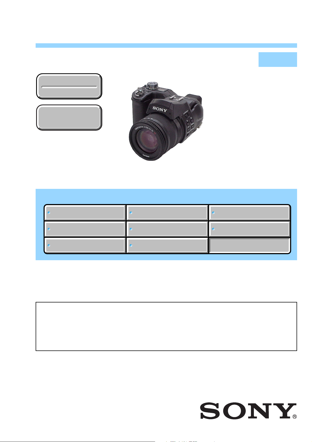
DSC-F828
SERVICE MANUAL
Ver 1.1 2004. 04
Revision History
Revision History
How to use
How to use
Acrobat Reader
Acrobat Reader
Link
Link
SPECIFICATIONS
SPECIFICATIONS
BLOCK DIAGRAMS
BLOCK DIAGRAMS
LEVEL 2
US Model
Canadian Model
AEP Model
UK Model
E Model
Hong Kong Model
Australian Model
Korea Model
Tourist Model
Chinese Model
Japanese Model
PRINTED WIRING BOARDS
PRINTED WIRING BOARDS
SERVICE NOTE
SERVICE NOTE
DISASSEMBLY
DISASSEMBLY
• For ADJUSTMENTS (SECTION 6), refer to SERVICE MANUAL, ADJ (987627951.pdf).
• For INSTRUCTION MANUAL, refer to SERVICE MANUAL, LEVEL 1 (987627941.pdf).
• Reference No. search on printed wiring boards is available.
• When the laser unit is repaired,
Make sure to follow the items of “NOTE ON HANDLING THE LASER DIODE”.
On the SY-096 board
This service manual provides the information that is premised the circuit board replacement service and not intended repair
inside the SY-096 board.
Therefore, schematic diagram, printed wiring board, mounted parts location and electrical parts list of the
shown.
The following pages are not shown.
Schematic diagram .............................Pages 4-25 to 4-44
Printed wiring board ............................Pages 4-59 to 4-62
FRAME SCHEMATIC DIAGRAMS
FRAME SCHEMATIC DIAGRAMS
SCHEMATIC DIAGRAMS
SCHEMATIC DIAGRAMS
Mounted parts location .............................
Electrical parts list ................................... Pages 5-14 to 5-18
REPAIR PARTS LIST
REPAIR PARTS LIST
SY-096 board
Pages 4-65 to 4-66
are not
DIGITAL STILL CAMERA
Page 2

DSC-F828
x Camera
[System]
Image device 11 mm (2/3 type) color
Total pixels number of camera
Effective pixels number of camera
Lens Carl Zeiss Vario-Sonnar T*
Exposure control
White balance
File format (DCF compliant)
Recording medium
Flash Recommended distance (when ISO
Viewfinder Electric viewfinder (color)
[Output connectors]
A/V OUT (MONO) jack (Monaural)
Accessory jack
USB jack mini-B
USB communication
CCD
4-color filter (RGBE)
Approx. 8 314 000 pixels
Approx. 8 068 000 pixels
7.1× zoom lens
f=7.1 to 51 mm
(35 mm camera conversion: 28 to
200 mm)
F2.0-2.8
Filter diameter: 58 mm (2
Automatic, Shutter speed priority,
Aperture priority, Manual exposure,
Scene selection (4 modes)
Automatic, Daylight, Cloudy,
Fluorescent, Incandescent, Flash,
One-push
Still images: Exif Ver. 2.2, JPEG
compliant, RAW, TIFF, DPOF
compatible
Audio with still image: MPEG1
compliant (Monaural)
Movies: MPEG1 compliant
(Monaural)
“Memory Stick”, Microdrive,
CompactFlash card (TypeI/TypeII)
sensitiv i ty is set to Auto)
0.5 to 4.5 m (19
1
14 feet 9
/4inches) (W)
0.6 to 3.3 m (23
10 feet 10 inches) (T)
Minijack
Video: 1 Vp-p, 75 Ω, unba lanced,
sync negative
Audio: 327 mV (at a 47 kΩ load)
Output impedance 2.2 kΩ
Mini-minijack (ø 2.5 mm)
Hi-Speed USB (USB 2.0 HighSpeed compliant)
3
/4inches to
5
/8inches to
3
/8inches)
SPECIFICATIONS
[LCD screen]
LCD panel used
Total number of dots
[Finder]
LCD panel used
Total number of dots
[Power, general]
Used battery pack
Power requirements
Power consumption (during shooting with LCD
Operating temperature range
Storage temperature range
Dimensions (lens: W-end)
Mass Approx. 95 5 g (33.7 oz) (battery
Microphone Electret condenser microphone
Speaker Dynamic speaker
Exif Print Compatible
PRINT Image Matching II
PictBridge Compatible
4.6 cm (1.8 type) TFT drive
134 400 (560×240) dots
1.1 cm (0.44 type) TFT drive
235 200 (980×240) dots
NP-FM50
7.2 V
screen on)
2.2 W
0° to+40°C (32° to +104°F)
(When using the Microdrive: +5° to
+40°C (41° to +104°F))
−20° to +60°C (−4° to +140°F)
134.4 91.1 157.2 mm
××
3
(5
/8 3×5/8× 6 1/4inches)
(W/H/D, protruding portions not
included)
pack NP-FM50, “Memory Stic k,”
shoulder strap, lens cap, and so on
included)
Compatible
x AC-L15A/L15B AC Adaptor
Power requirements
Current consumption
Power consumption
Output voltage
Operating temperature range
Storage temperature range
Maximum dimensions
Mass Approx. 190 g (6.7 oz) excluding
AC 100 − 240 V, 50/60 Hz
0.35 − 0.18 A
18 W
8.4 V DC, 1.5 A
0° to +40°C (32° to +104°F)
−20° to +60°C (−4° to +140°F)
Approx. 56 × 31 × 100 mm
1
(2
/4 × 1 1/4 × 4inches) (W/H/D),
excluding projecting parts
power cord (mains lead)
x NP-FM50 battery pack
Used battery
Maximum voltage
Nominal voltage
Capacity 8.5 Wh (1 180 mAh)
Lithium-ion battery
DC 8.4 V
DC 7.2 V
Accessories
• AC Adaptor (1)
• Power cord (mains lead) (1)
• USB cable (1)
• Battery pack NP-FM50 (1)
• A/V connecting cable (1)
• Shoulder strap (1)
• Lens cap (1)
• Lens cap strap (1)
• Lens hood (1)
• CD-ROM (USB driver: SPVD-013) (1)
• CD-ROM (Image Data Converter) (1)
• Operating Instructions (1)
Design and specifications are subject to change
without notice.
— 2 —
Page 3
CAUTION
Use of controls or adjustments or performance
procedures other than those specified herein may
result in hazardous radiation exposure.
CAUTION :
Danger of explosion if battery is incorrectly replaced.
Replace only with the same or equivalent type.
DSC-F828
SAFETY-RELATED COMPONENT WARNING!!
COMPONENTS IDENTIFIED BY MARK 0 OR DOTTED LINE WITH
MARK 0 ON THE SCHEMATIC DIAGRAMS AND IN THE PARTS
LIST ARE CRITICAL TO SAFE OPERATION. REPLACE THESE
COMPONENTS WITH SONY PARTS WHOSE PART NUMBERS
APPEAR AS SHOWN IN THIS MANUAL OR IN SUPPLEMENTS
PUBLISHED BY SONY.
SAFETY CHECK-OUT
After correcting the original service problem, perform the following
safety checks before releasing the set to the customer.
1. Check the area of your repair for unsoldered or poorly-soldered
connections. Check the entire board surface for solder splashes
and bridges.
2. Check the interboard wiring to ensure that no wires are
"pinched" or contact high-wattage resistors.
3. Look for unauthorized replacement parts, particularly
transistors, that were installed during a previous repair. Point
them out to the customer and recommend their replacement.
4. Look for parts which, through functioning, show obvious signs
of deterioration. Point them out to the customer and
recommend their replacement.
5. Check the B+ voltage to see it is at the values specified.
6. Flexible Circuit Board Repairing
• Keep the temperature of the soldering iron around 270˚C
during repairing.
• Do not touch the soldering iron on the same conductor of the
circuit board (within 3 times).
• Be careful not to apply force on the conductor when soldering
or unsoldering.
ATTENTION AU COMPOSANT AYANT RAPPORT
À LA SÉCURITÉ!
LES COMPOSANTS IDENTIFÉS PAR UNE MARQUE 0 SUR LES
DIAGRAMMES SCHÉMATIQUES ET LA LISTE DES PIÈCES SONT
CRITIQUES POUR LA SÉCURITÉ DE FONCTIONNEMENT. NE
REMPLACER CES COMPOSANTS QUE PAR DES PIÈSES SONY
DONT LES NUMÉROS SONT DONNÉS DANS CE MANUEL OU
DANS LES SUPPÉMENTS PUBLIÉS PAR SONY.
Unleaded solder
Boards requiring use of unleaded solder are printed with the leadfree mark (LF) indicating the solder contains no lead.
(Caution: Some printed circuit boards may not come printed with
the lead free mark due to their particular size.)
: LEAD FREE MARK
Unleaded solder has the following characteristics.
• Unleaded solder melts at a temperature about 40°C higher than
ordinary solder.
Ordinary soldering irons can be used but the iron tip has to be
applied to the solder joint for a slightly longer time.
Soldering irons using a temperature regulator should be set to
about 350°C.
Caution: The printed pattern (copper foil) may peel away if the
heated tip is applied for too long, so be careful!
• Strong viscosity
Unleaded solder is more viscous (sticky, less prone to flow) than
ordinary solder so use caution not to let solder bridges occur such
as on IC pins, etc.
• Usable with ordinary solder
It is best to use only unleaded solder but unleaded solder may
also be added to ordinary solder.
— 3 —
Page 4

DSC-F828
TABLE OF CONTENTS
1. SERVICE NOTE
1-1. NOTE FOR REPAIR······················································· 1-1
1-2. DISCHARGING OF THE FLASH UNIT’S CHARGING
CAPACITOR ···································································1-1
1-2-1.Preparing the Short Jig ····················································1-1
1-2-2.Discharging the Capacitor ···············································1-1
1-3. NOTES ON HANDLING THE LASER DIODE
[LASER UNIT] ······························································· 1-2
1-4. DESCRIPTION ON SELF-DIAGNOSIS DISPLAY······1-2
2. DISASSEMBLY
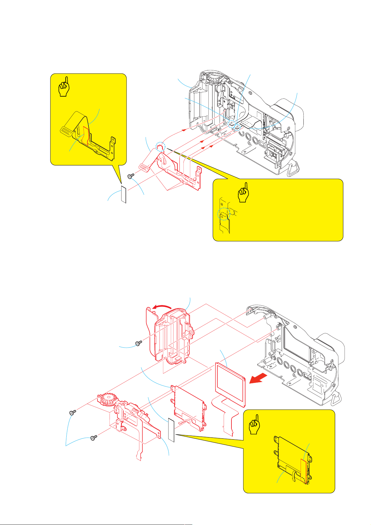
2-1. CABINET (LR) ASSEMBLY, SW-410 BOARD············ 2-2
2-2. STROBOSCOPE BLOCK ASSEMBLY·························2-3
2-3. ST SECTION ··································································2-4
2-4. ST-088 BOARD, LENS SECTION································· 2-4
2-5. ST CABINET ASSEMBLY ············································2-5
2-6. MT-067 BOARD ·····························································2-5
2-7. SI-037 BOARD, FLASH UNIT ······································2-6
2-8. LS-067 BOARD, LASER UNIT ·····································2-7
2-9. REAR CABINET BLOCK ASSEMBLY ························2-8
2-10. EVF SECTION ································································2-8
2-11. CONTROL SWITCH BLOCK (UNDER) ······················2-9
2-12. CONTROL SWITCH BLOCK (MID), LCD UNIT ······· 2-9
2-13. BTH SECTION ·····························································2-10
2-14. SY-096 BOARD ····························································2-11
2-15. DD-204 BOARD ··························································· 2-12
2-16. CF-097 BOARD ····························································2-12
2-17. LR-018 BOARD, LITHIUM BATTERY ······················2-13
2-18. MEMORY STICK CONNECTOR ·······························2-13
2-19. AJ-007 BOARD ···························································· 2-14
2-20. DC-IN CONNECTOR, UA-003 BOARD·····················2-14
2-21. FP-747/746/754 FLEXIBLE BOARD ··························2-15
2-22. HINGE/CABINET (LL) ASSEMBLY·························· 2-16
2-23. SPEAKER/MICROPHONE SECTION ························2-16
2-24. CABINET UPPER ASSEMBLY ·································· 2-17
2-25. CONTROL SWITCH BLOCK (TOP) ··························2-19
2-26. CIRCUIT BOARDS LOCATION ·································2-20
2-27. CIRCUIT BOARDS AND
FLEXIBLE BOARDS LOCATION ······························2-21
3. BLOCK DIAGRAMS
3-1. OVERALL BLOCK DIAGRAM (1/3) ···························3-1
3-2. OVERALL BLOCK DIAGRAM (2/3) ···························3-3
3-3. OVERALL BLOCK DIAGRAM (3/3) ···························3-5
3-4. POWER BLOCK DIAGRAM (1/2)································3-7
3-5. POWER BLOCK DIAGRAM (2/2)································3-9
4. PRINTED WIRING BOARDS AND
SCHEMATIC DIAGRAMS
4-1. FRAME SCHEMATIC DIAGRAM (1/4) ·······················4-1
FRAME SCHEMATIC DIAGRAM (2/4)·······················4-3
FRAME SCHEMATIC DIAGRAM (3/4)·······················4-5
FRAME SCHEMATIC DIAGRAM (4/4)·······················4-7
4-2. SCHEMATIC DIAGRAMS
• DD-204 (DC/DC CONVERTER)
SCHEMATIC DIAGRAM····························4-11
• LR-018 (BATTERY, RESET SW)
SCHEMATIC DIAGRAM····························4-12
• ST-088 (FLASH CONTROL)
SCHEMATIC DIAGRAM····························4-13
• LS-067 (AF LASER)
SCHEMATIC DIAGRAM····························4-13
• MT-067 (FLASH MOTOR)
SCHEMATIC DIAGRAM····························4-14
• SI-037 (FLASH, IR LED)
SCHEMATIC DIAGRAM····························4-14
• AS-050 FLEXIBLE
SCHEMATIC DIAGRAM····························4-14
• UA-003 (AV, USB JACK)
SCHEMATIC DIAGRAM····························4-15
• LB-091 (EVF, EVF BACK LIGHT)
SCHEMATIC DIAGRAM····························4-16
• CF-097 (CF CARD CONNECTOR)
SCHEMATIC DIAGRAM····························4-17
• FP-756 FLEXIBLE
SCHEMATIC DIAGRAM····························4-17
• SW-410 (FUNCTION KEY)
SCHEMATIC DIAGRAM····························4-19
• AJ-007 (JACK)
SCHEMATIC DIAGRAM····························4-19
• CONTROL SWITCH BLOCK (TOP)
SCHEMATIC DIAGRAM····························4-21
• CONTROL SWITCH BLOCK (MID)
SCHEMATIC DIAGRAM····························4-22
• CONTROL SWITCH BLOCK (UNDER)
SCHEMATIC DIAGRAM····························4-23
Schematic diagrams of the SY-096 board are not
shown.
Pages from 4-25 to 4-44 are not shown.
4-3. PRINTED WIRING BOARDS
• DD-204 (DC/DC CONVERTER)
PRINTED WIRING BOARD ·······················4-49
• LR-018 (BATTERY, RESET SW)
PRINTED WIRING BOARD ·······················4-50
• ST-088 (FLASH CONTROL)
PRINTED WIRING BOARD ·······················4-51
• MT-067 (FLASH MOTOR)
PRINTED WIRING BOARD ·······················4-51
• LS-067 (AF LASER)
PRINTED WIRING BOARD ·······················4-52
• SI-037 (FLASH, IR LED)
PRINTED WIRING BOARD ·······················4-53
• UA-003 (AV, USB JACK)
PRINTED WIRING BOARD ·······················4-54
• LB-091 (EVF, EVF BACK LIGHT)
PRINTED WIRING BOARD ·······················4-54
• CF-097 (CF CARD CONNECTOR)
PRINTED WIRING BOARD ·······················4-55
• AJ-007 (JACK)
PRINTED WIRING BOARD ·······················4-56
• SW-410 (FUNCTION KEY)
PRINTED WIRING BOARD ·······················4-57
• FP-748 (CONNECTOR)
PRINTED WIRING BOARD ·······················4-57
Printed wiring board of the SY-096 board is not
shown.
Pages from 4-59 to 4-62 are not shown.
4-4. MOUNTED PARTS LOCATION ·································4-63
Mounted parts location of the SY-096 board is not
shown.
Page 4-65 to 4-66 are not shown.
5. REPAIR PARTS LIST
5-1. EXPLODED VIEWS ······················································5-3
5-1-1.OVERALL SECTION·····················································5-3
5-1-2.STROBOSCOPE BLOCK ASSEMBLY·························5-4
5-1-3.CABINET (FRONT) BLOCK ASSEMBLY-1 ················5-5
5-1-4.CABINET (FRONT) BLOCK ASSEMBLY-2 ················5-6
— 4 —
Page 5

5-1-5.BTH BLOCK ASSEMBLY ·············································5-7
5-1-6.CABINET (REAR) BLOCK ASSEMBLY ·····················5-8
5-1-7.EVF ASSEMBL Y····························································5-9
5-2. ELECTRICAL PARTS LIST ········································5-10
Parts list of the SY-096 board are not shown.
Pages from 5-14 to 5-18 are not shown.
DSC-F828
— 5 —
Page 6
1-1. NOTE FOR REPAIR
DSC-F828
SECTION 1
SERVICE NOTE
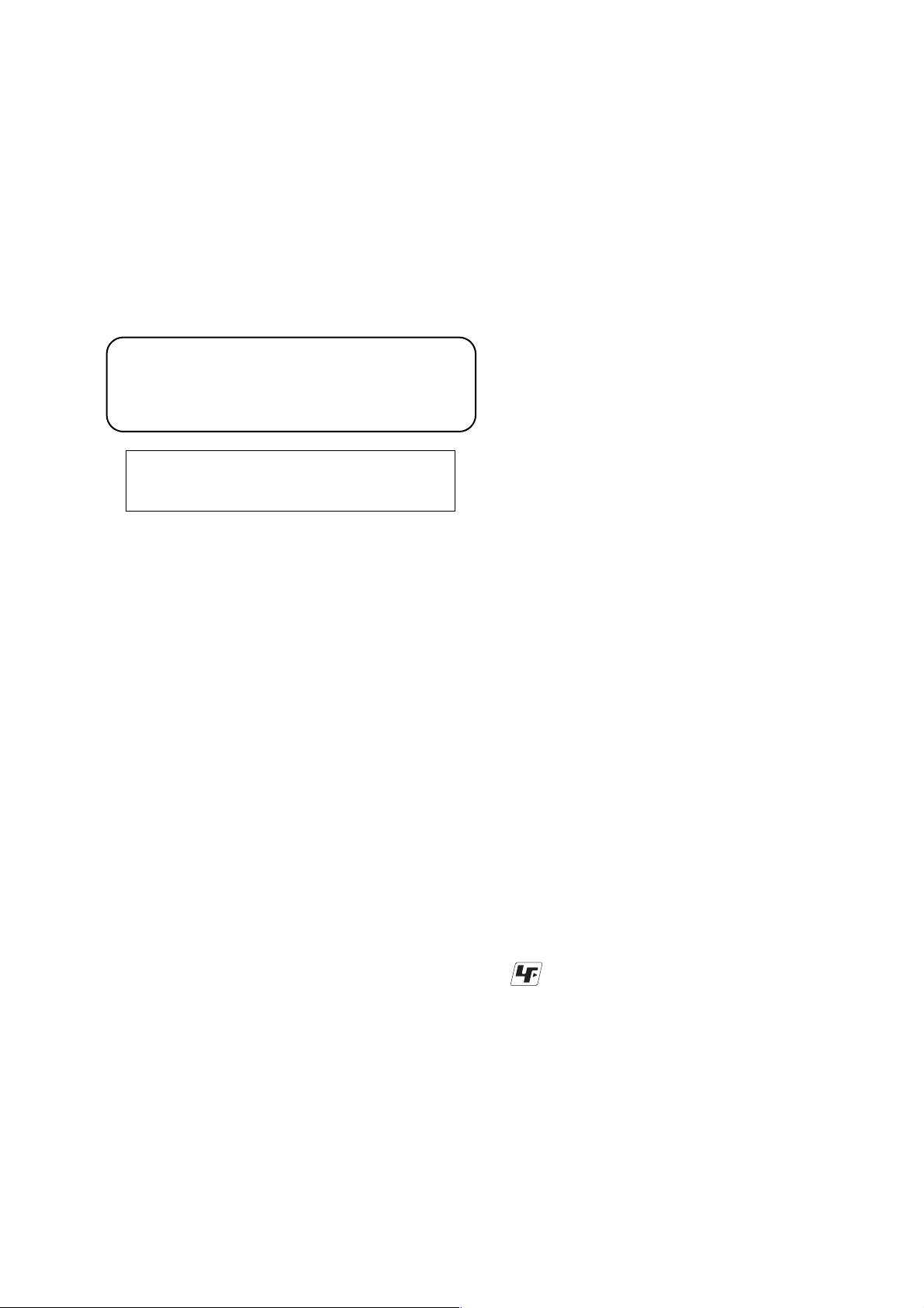
Make sure that the flat cable and flexible board are not cracked of
bent at the terminal.
Do not insert the cable insufficiently nor crookedly.
Cut and remove the part of gilt
which comes off at the point.
(Take care that there are
some pieces of gilt left inside)
When remove a connector, don't pull at wire of connector.
Be in danger of the snapping of a wire.
When installing a connector, don't press down at wire of connector.
Be in danger of the snapping of a wire.
1-2. DISCHARGING OF THE FLASH UNIT’S CHARGING CAPACITOR
The charging capacitor of the FLASH unit is charged up to the maximum 300 V potential.
There is a danger of electric shock by this high voltage when the capacitor is handled by hand. The electric shock is caused by the charged
voltage which is kept without discharging when the main power of the DSC-F828 is simply turned off. Therefore, the remaining voltage
must be discharged as described below.
1-2-1. Preparing the Short Jig
To preparing the short jig. a small clip is attached to each end of a
resistor of 1 kΩ /1 W (1-215-869-11)
Wrap insulating tape fully around the leads of the resistor to prevent
electrical shock.
1 kΩ/1 W
Wrap insulating tape.
1-2-2. Discharging the Capacitor
Short circuits between the positive and the negative terminals of
charged capacitor with the short jig about 10 seconds.
Short jig
Ω
/1W)
(1k
DD-204
DD-204 board
1-1
Page 7
DSC-F828
1-3. NOTES ON HANDLING THE LASER DIODE [LASER UNIT]
The laser diode may suffer electrostatic breakdown because of the
potential difference generated by the charged electrostatic load, etc.
on clothing and the human body.
During repair, pay attention to electrostatic breakdown and also use
the procedure in the printed matter which is included in the repair
parts.
The flexible board is easily damaged and should be handled with
care.
Soldering Conditions of Laser Unit
Temperature of Less than 350 °C
the Soldering Iron
Time to Solder 3 seconds
Interval to Solder Next terminal is soldered after waiting
for 1 second
Note: Adjustment is needed when laser unit is replaced.
Laser unit
(D001)
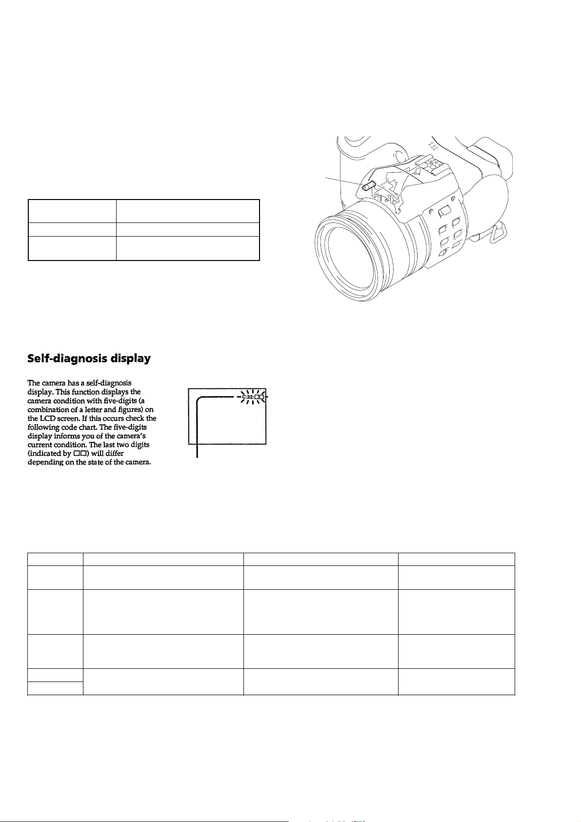
1-4. DESCRIPTION ON SELF-DIAGNOSIS DISPLAY
Refer to “21. AF Laser Output Adjustment” (page6-29) and “22.
AF Laser Axis Check” (page6-30) of SERVICE MANUAL, ADJ
(987627951.pdf).
Self-diagnosis display
• C: ss: ss
The contents which can be handled
by customer, are displayed.
• E: ss: ss
The contents which can be handled
by engineer, are displayed.
Display Code
C:32:01
C:13:01
E:91:01
E:61:00 *1
E:61:10 *1
Note : The error code is cleared if the battery is removed, except defective flash unit.
*1: The error display is given in two ways.
Turn off the main power then back on.
Replace the memory stick.
Format the memory stick with the DSC-F828.
Checking of flash unit or replacement of
flash unit.
Checking of lens drive circuit
Countermeasure
Trouble with hardware.
• The type of memory stick that cannot be
used by this machine, is inserted.
• Data is damaged.
• Unformatted memory stick is inserted.
Abnormality when flash is being
charged.
When failed in the focus initialization.
Cause
Caution Display During Error
SYSTEM ERROR
MEDIA ERROR
Flash LED
Flash display
Flashing at 3.2 Hz
—
1-2E
Page 8
DSC-F828
SECTION 2
DISASSEMBLY
The following flow chart shows the disassembly procedure.
DISASSEMBLY
HELP
HELP
DISASSEMBLY
HELP
HELP
DISASSEMBLY
DISASSEMBLY
HELP
DISASSEMBLY
HELP
DISASSEMBLY
DISASSEMBLY
Discharging the Capacitor
4
0
2
-
D
D
HELP
DISASSEMBLY
HELP
HELP
DISASSEMBLY
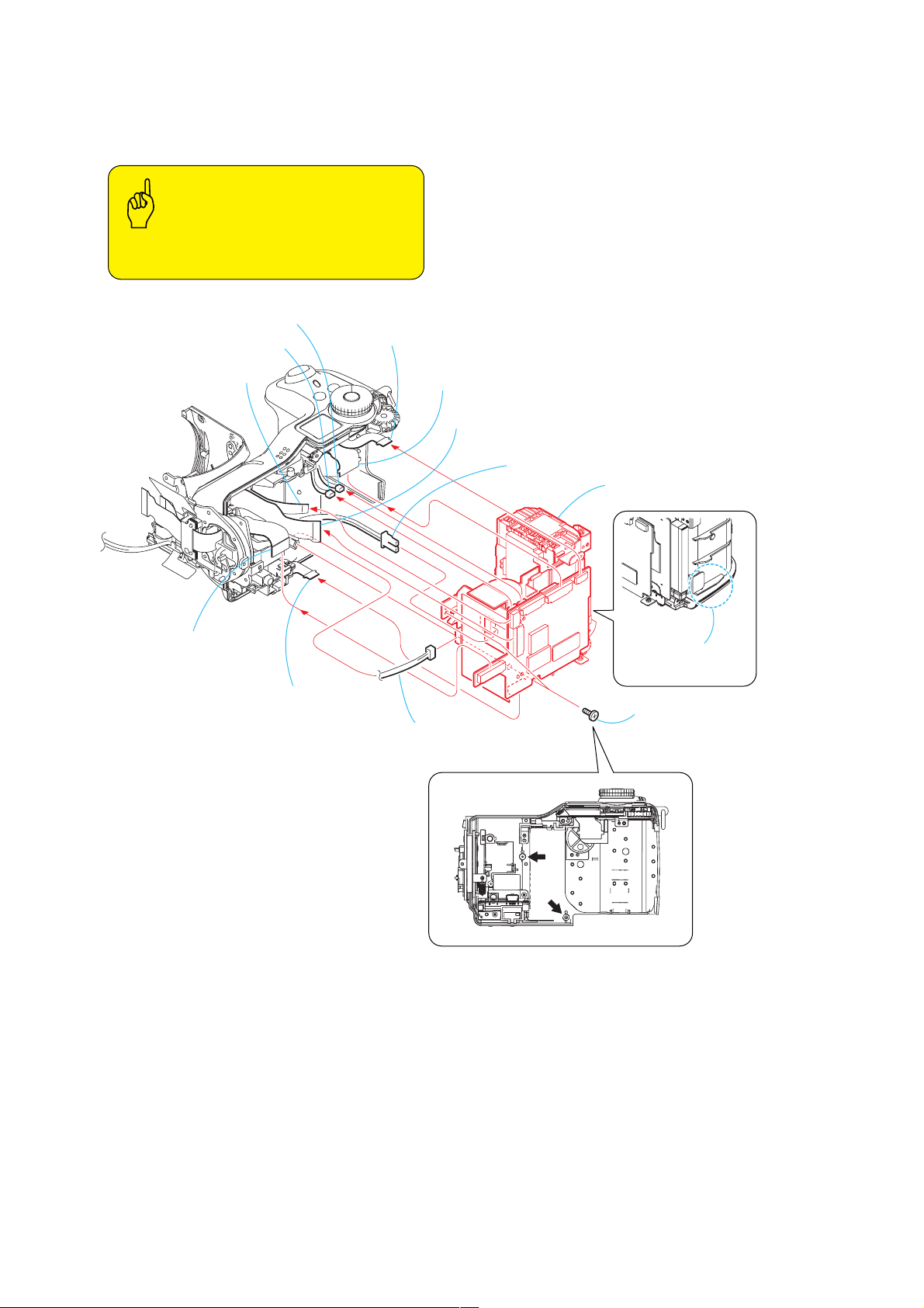
PROCEDURE OF REMOVING THE SY-096 BOARD (SERVICE POSITION)
1 2-1. CABINET (LR) ASSEMBLY, SW-410 BOARD ................................
2 2-2. STROBOSCOPE BLOCK ASSEMBLY ...........................................
3 2-9. REAR CABINET BLOCK ASSEMBLY ...........................................
4 2-13. BTH SECTION ..............................................................................
5 2-14. SY-096 BOARD .............................................................................
6 2-15. DD-204 BOARD ............................................................................
7 2-16. CF-097 BOARD ............................................................................
8 2-18. MEMORY STICK CONNECTOR ..................................................
9 2-20. DC-IN CONNECTOR,UA-003 BOARD .........................................
q; 2-21. FP-747/746/754 FLEXIBLE BOARD ............................................
qa 2-24. CABINET UPPER ASSEMBLY .....................................................
(page 2-2)
(page 2-3)
(page 2-8)
(page 2-10)
(page 2-11)
(page 2-12)
(page 2-12)
(page 2-13)
(page 2-14)
(page 2-15)
(page 2-17)
HELP
DISASSEMBLY
HELP
DISASSEMBLY
SY-096 board
service position
2-1
Page 9
DSC-F828
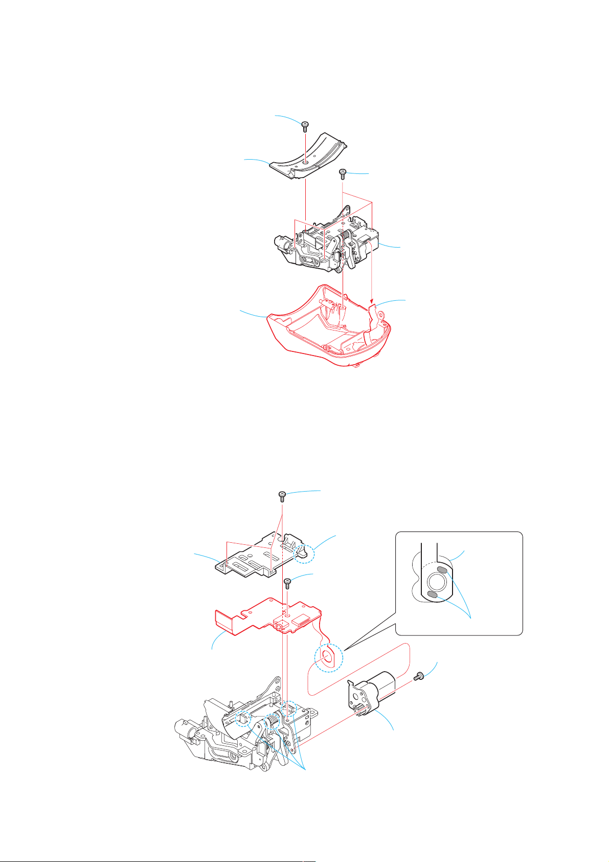
NOTE: Follow the disassembly procedure in the numerical order given.
2-1. CABINET (LR) ASSEMBLY, SW-410 BOARD
2
FP-751 flexible board
(6P)
5
Tape (A)
Caution
Note: When installing, be careful not to pinch
the extra length of flexible board because
it can be easily pinched during installation.
FP-751 flexible board
3
Three screws (M2 × 4), lock ace
7
SW-410 board
6
FP-751
flexible board (6P)
4
Cabinet (LR) assembly
Tape (A)
1
Six screws (M2 × 4),
lock ace
2-2
Page 10
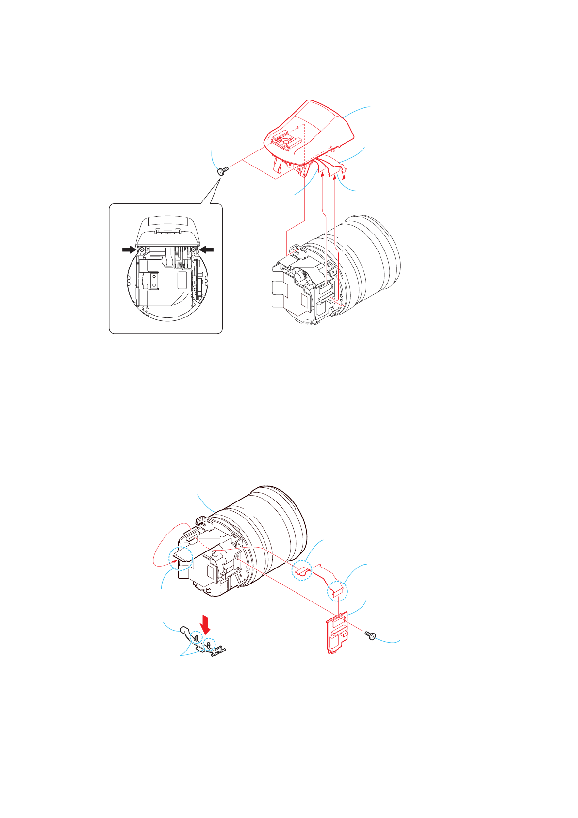
2-2. STROBOSCOPE BLOCK ASSEMBLY
5
FP-746 flexible board
(51P)
4
FP-747 flexible board
(51P)
7
AJ-006 flexible board
(6P)
6
FP-754 flexible board
(21P)
Adhesion side (Ferrite core)
q;
Stroboscope block assembly
9
harness (PT132)
harness
(PT132)
8
Two screws
(M2
×
4), lock ace
ST-088 board
ST-088 board
2
Peel the Radiation sheets (LR)
from flexible boards.
Radiation sheet (LR)
3
Claw
1
Tapping screw
(M1.7
×
4)
Tapping screw
(M1.7
×
4)
Dowel
Harness processing
Caution
Note: Be careful not to drop
the f
errite core.
DSC-F828
2-3
Page 11
DSC-F828
2-3. ST SECTION
1
Two screws (M2 × 4),
lock ace
4
MT-067 board
(16P)
5
ST section
2
LS-067 board
(6P)
3
SI-037 board (26P)
2-4. ST-088 BOARD, LENS SECTION
8
Lens section
4
Flexible board (Lens)(39P)
7
Harness guide
6
Two claws
5
FP-750 flexible board
(22P)
2
FP-750 flexible board
(22P)
3
ST-088 board
1
Screw (M1.7 × 3),
lock ace
2-4
Page 12
2-5. ST CABINET ASSEMBLY
2
Tapping screw
(M1.7
3
ST blind cover
5
ST cabinet assembly
DSC-F828
×
4)
4
Four tapping screws
×
(M1.7
4)
6
ST section
1
AS-050 flexible board
(10P)
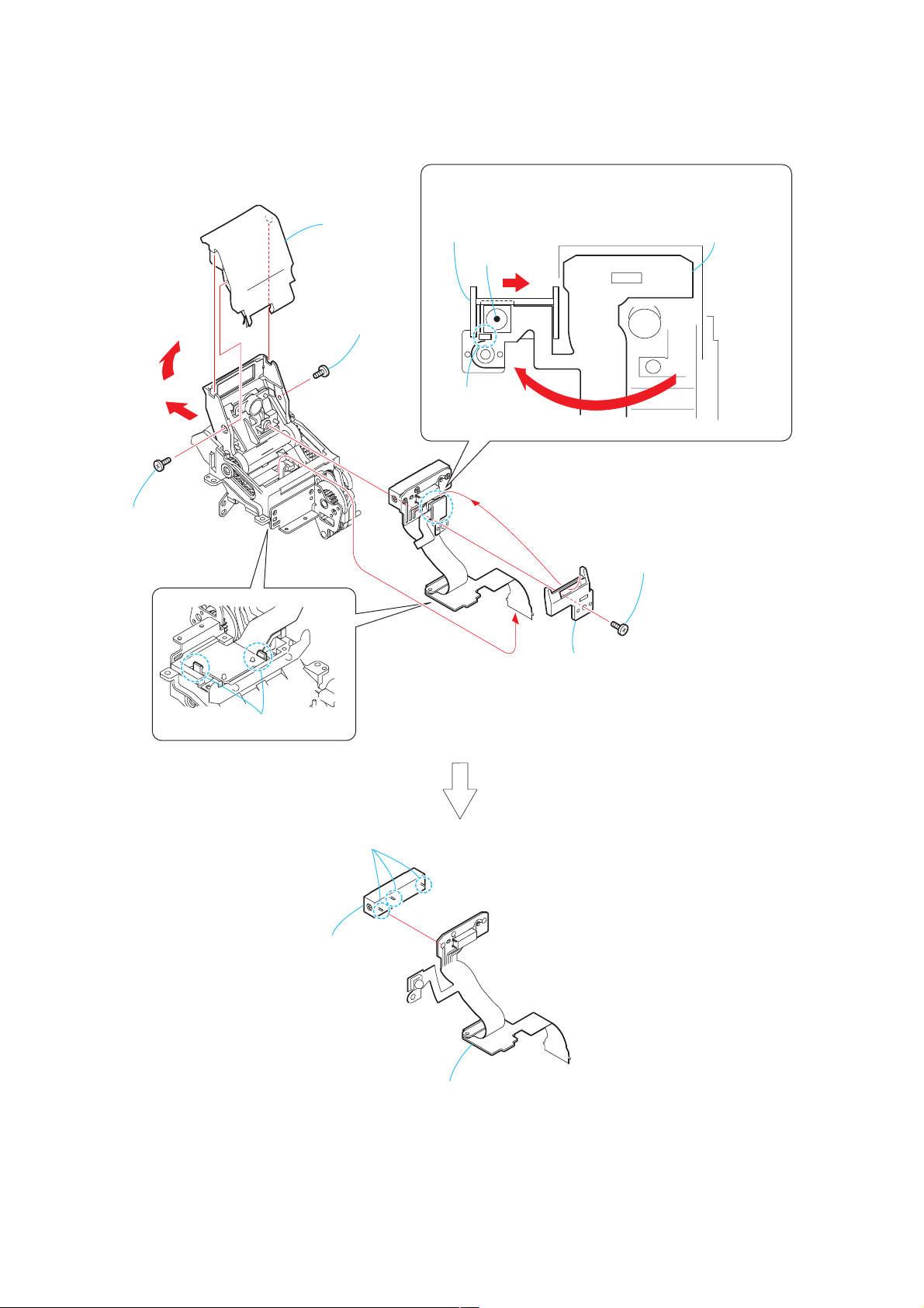
2-6. MT-067 BOARD
3
STFPC cover
9
MT-067 board
1
Three tapping screws
(M1.7
4
Screw (M1.7 × 2),
grip
2
Claw
×
4)
6
Remove the two solderings.
7
Stroboscope motor
Stroboscope motor
5
Screw (M1.7 × 2),
grip
8
Three claws
2-5
Page 13
DSC-F828
2-7. SI-037 BOARD, FLASH UNIT
2
1
5
ST cover
3
Tapping screw
(M1.7 × 4)
Remove the ST unit holder from the SI-037 board by disengaging
the claw while sliding the (A) section of the SI-037 board in the
direction of the arrow (B).
ST unit holder
(A) Section
8
Claw
(B)
7
Open the ST unit holder section
SI-037 board
4
Tapping screw
(M1.7 × 4)
q;
Two claws
qa
Remove soldering from the three points
qs
Flash unit
6
Tapping screw
(M1.7 × 4)
9
ST unit holder
qd
SI-037 board
2-6
Page 14
2-8. LS-067 BOARD, LASER UNIT
2
Two dowels
1
Tapping screw
(M1.7
×
DSC-F828
4)
4
3
Two grooves
6
Laser unit (D001)
ST laser holder
5
Remove the
three solderings
Caution
When soldering the laser unit on the LS-067 board,
observe the following things.
(Refer to Service Note (page 1-2)).
Observe the following conditions of temperature
and time of soldering.
Temperature of soldering iron : 350
Time of contacting the soldering : 3 seconds
iron with the solder
The laser diode may suffer electrostatic breakdown
because of the potential difference generated by the
charged electrostatic load, etc. on clothing and the
human body.
During repair, pay attention to electrostatic breakdown
and also use the procedure in the printed matter which
is included in the repair parts.
The flexible board is easily damaged and should be
handled with care.
°
C
7
LS-067 board
2-7
Page 15
DSC-F828
)
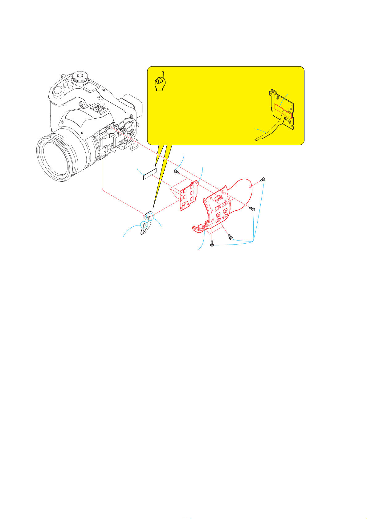
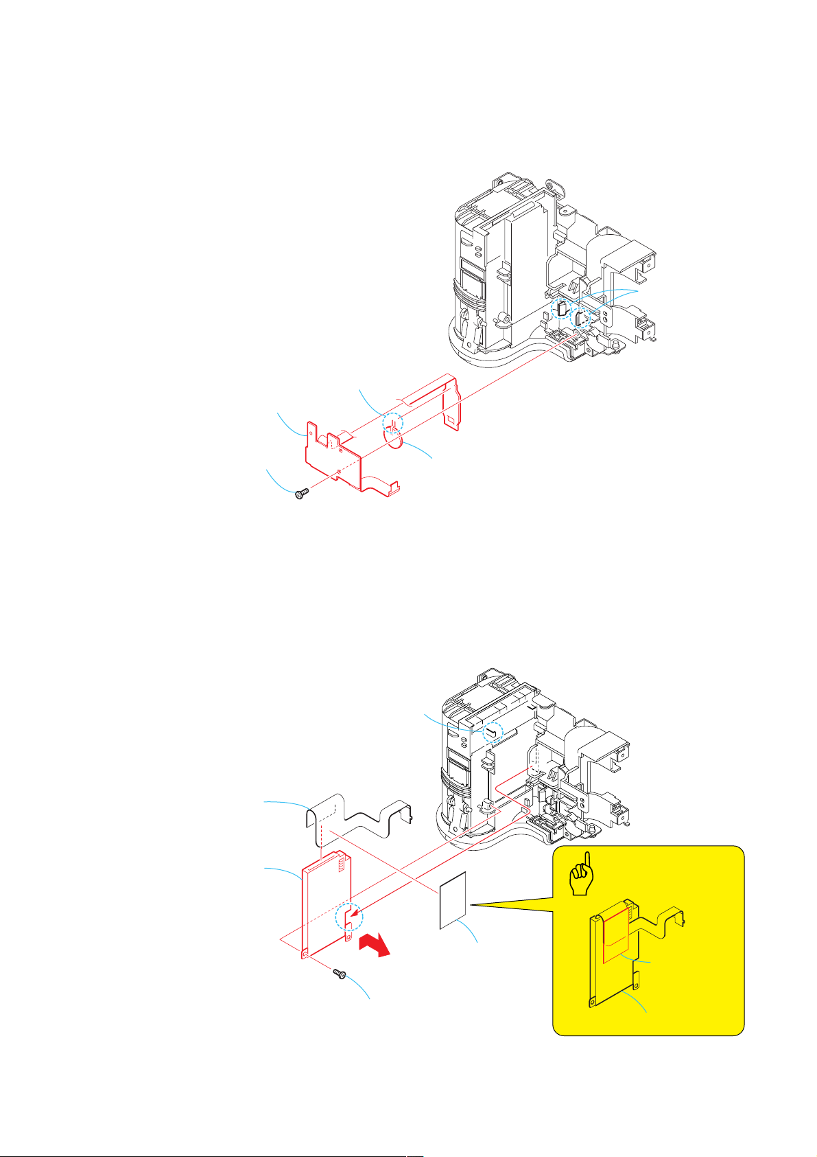
2-9. REAR CABINET BLOCK ASSEMBLY
6
LB-091 board
(22P)
5
Screw (M2 × 4), lock ace
Caution
The LB-091 board may be damaged if you
remove the rear cabinet block assembly forcibly.
Be very careful not to damage the flexible board.
4
Screw (M2 × 4),
lock ace
2
Screw (M2 × 4),
lock ace
2-10.EVF SECTION
7
Control switch block (under)
(50P)
1
Two screws (M2 × 4),
lock ace
7
8
LB-091 board
8
Rear cabinet block assembly
4
Prism sheet
5
Illuminator
Two claws
3
Two screws (M2 × 4),
lock ace
3
Three claws
6
LCD (LCX044AK-1
(18P)
1
Four tapping screws
×
(M1.7
4)
2
EVF section
2-8
q;
LCD (LCX044AK-1)
9
Lamp guide (20)
Page 16
2-11.CONTROL SWITCH BLOCK (UNDER)
5
Cabinet (rear) assembly
Caution
2
Control switch block
Control switch block (under)
Tape (A)
(mid)(10p)
7
Control switch block
(under)
3
Block light guide plate (6P)
4
LCD module (24P)
DSC-F828
1
6
Tape (A)
Three screws (M1.7 × 3),
lock ace
2-12.CONTROL SWITCH BLOCK (MID), LCD UNIT
8
CF lid assembly
2
Open the CF lid
7
Two screws (M1.7 × 3),
lock ace
5
Block light guide plate
6
LCD unit
Caution
Install the control switch block (under) in the
cabinet (rear) assembly so that the tip of the
control switch block (under) go under the
bottom of the control switch block (mid).
1
Five screws (M1.7 × 3),
lock ace
4
Tape (A)
3
Control switch block (mid)
2-9
Caution
Tape (A)
Block light guide plate
Page 17
DSC-F828
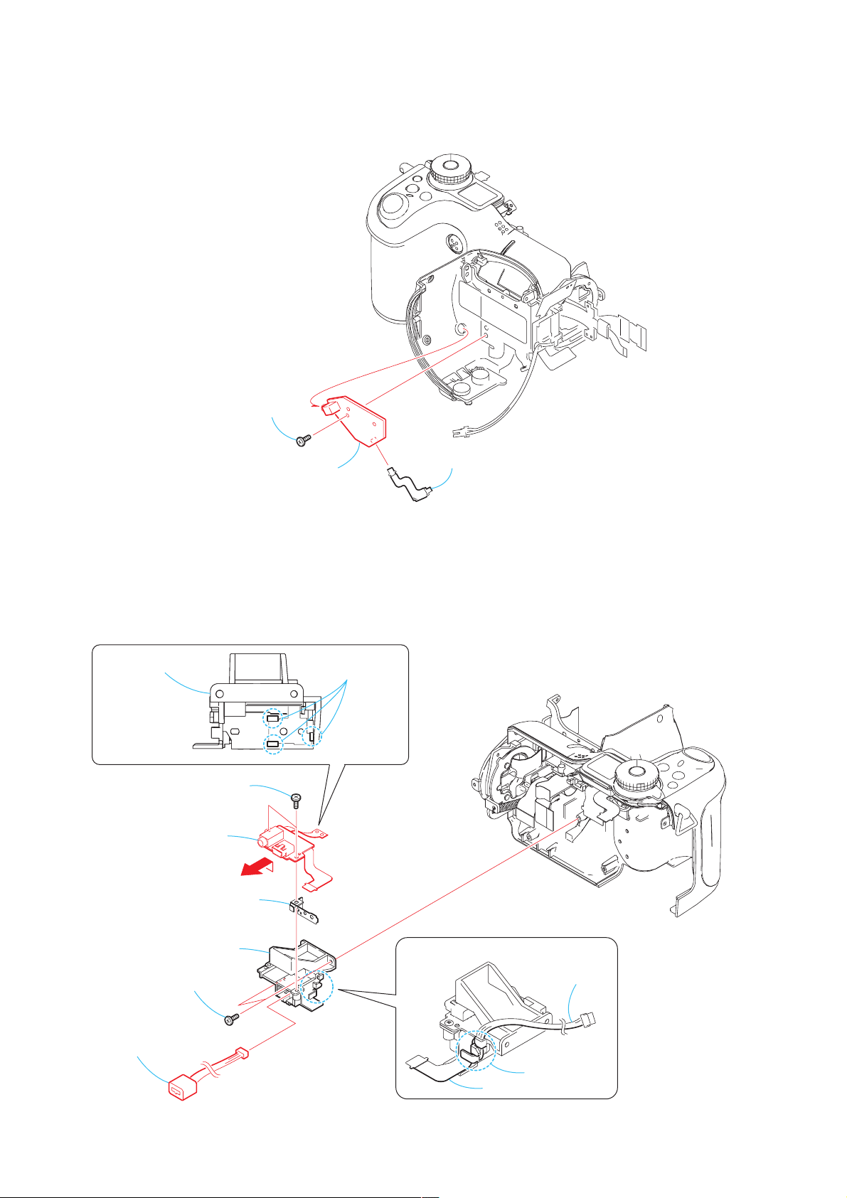
2-13.BTH SECTION
Note: When installing, be careful not to pinch
the flexible board or harness during installation.
1
FP-754 flexible board
(21P)
Caution
6
Harness (microphone)
7
Harness (speaker)
4
Control switch block (top)
(12P)
5
LCD module (26P)
2
FP-746 flexible board
(51P)
q;
Harness (PT-132)
qs
BTH section
3
FP-747 flexible board
(51P)
8
UA-003 board
(12P)
qa
Connector (3P)
Use the groove on side
when installing it.
9
Two screws (M1.7 × 3),
lock ace
2-10
Page 18
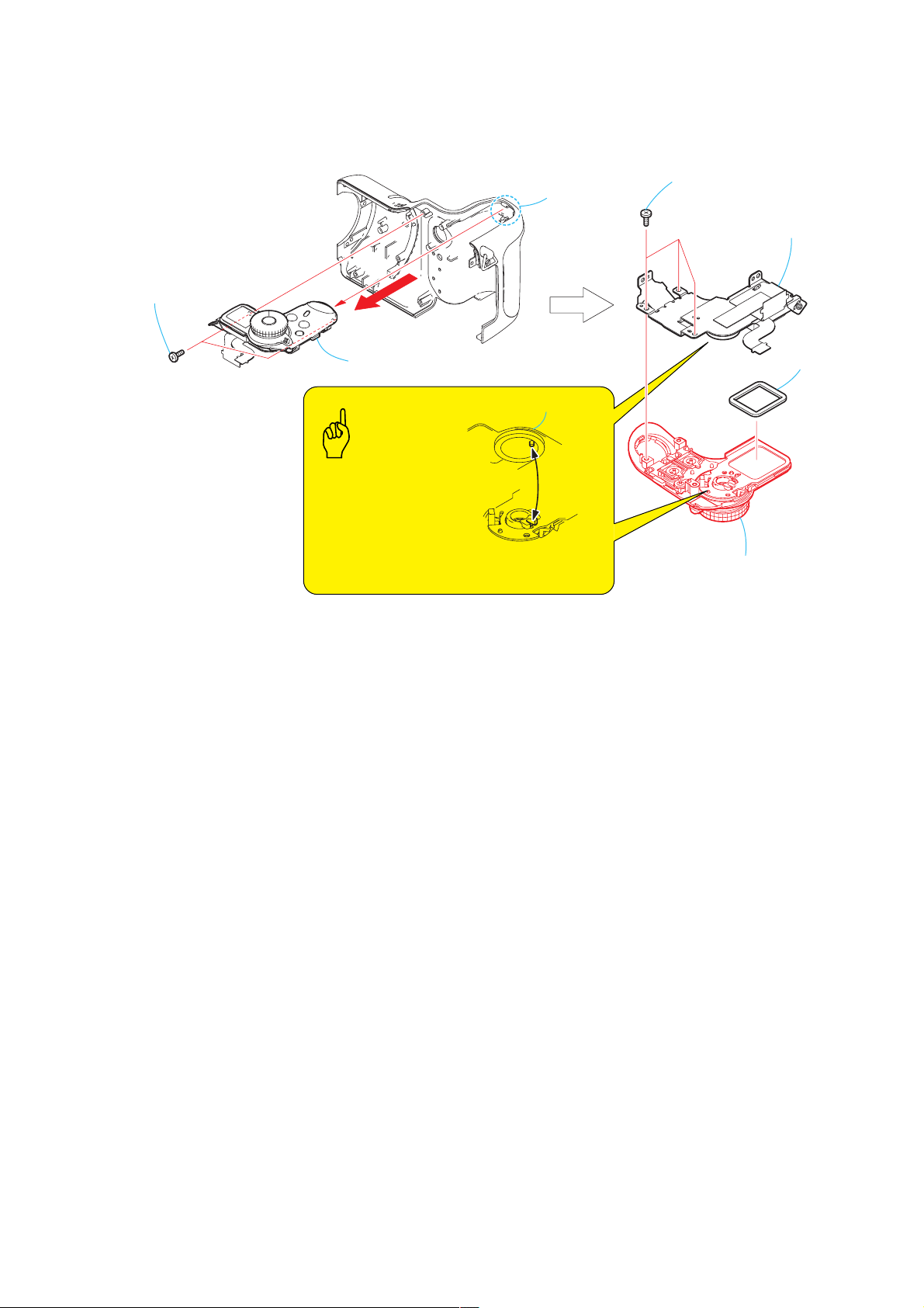
2-14.SY-096 BOARD
3
FP-748 board
(60P)
5
Cushion (SY)
2
FP-749 flexible board
(10P)
4
FP-756 flexible board
(51P)
6
SY-096 board
1
Two screws (M1.7 × 3),
lock ace
DSC-F828
Caution
Cushion (SY)
SY-096 board
2-11
Page 19
DSC-F828
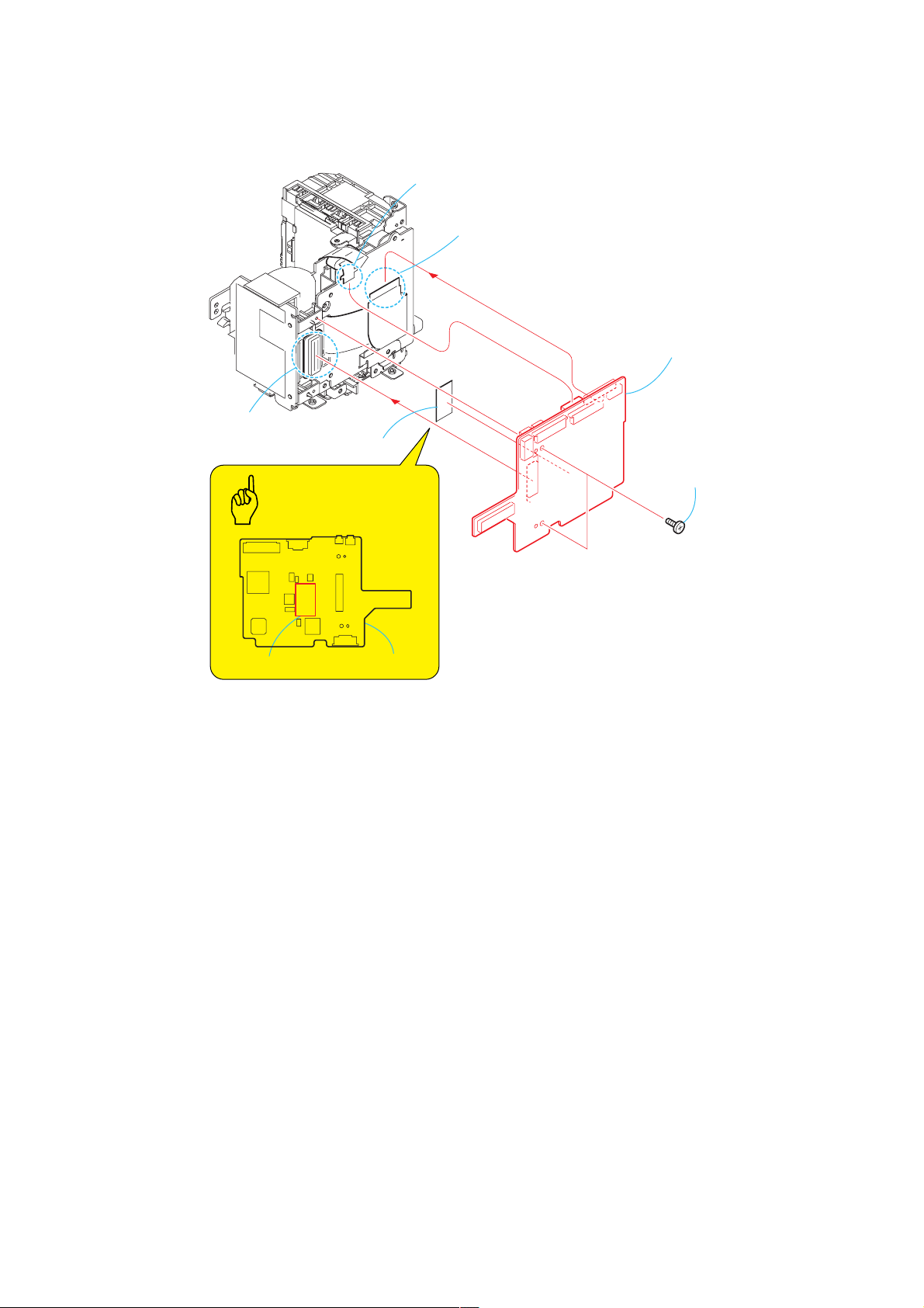
2-15.DD-204 BOARD
4
Two claws
3
LR-018 board (6P)
Caution
Note: The power supply capacitor of the flash unit is charged to the high tension
voltage as high as 300 V at a maximum. You will get electrical shock when
you touch the terminal of the charged capacitor . The charged potential
remains even after the main power of the machine is turned off. Discharge
the remaining power in the capacitor referring to Service Note
(See page 1-1). High-voltage cautions. Short jig (R: 1k Ω /1W)
6
FP-748 board
7
Remove soldering from two point
9
DD-204 board
2
Two screws (M1.7 × 3)
lock ace
5
Battery terminal board (3P)
2-16.CF-097 BOARD
8
Capacitor
Caution
DD-204 board
Fuse replacement caution label
4
Tape (A)
DD-204
1
Fuse replacement caution label
Caution
Tape (A)
3
FP-756 flexible board
(51P)
6
CF-097 board
5
Ferrite bead
2-12
Ferrite bead
2
SY retainer
1
Four screws (M1.7 × 3)
lock ace
FP-749 flexible board
Page 20
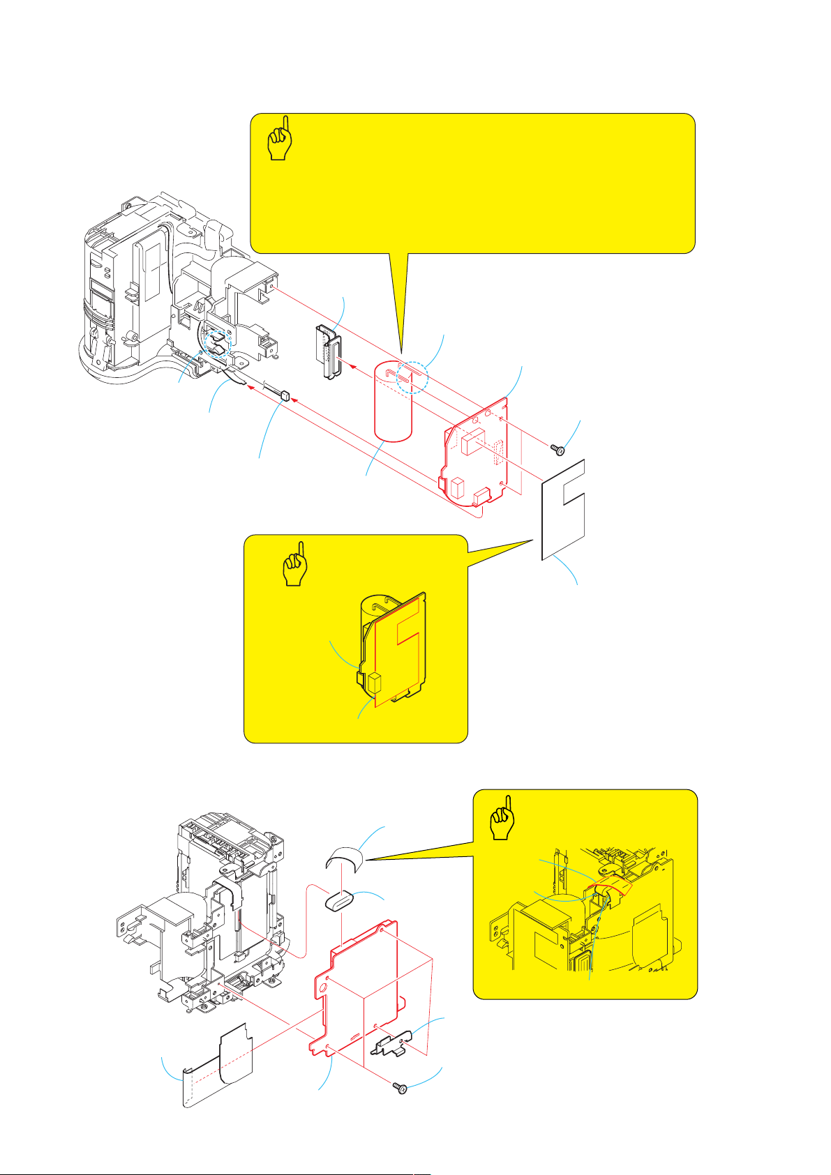
2-17.LR-018 BOARD, LITHIUM BATTERY
s
4
Remove soldering
from the two points.
3
LR-018 board
2
Two claw
DSC-F828
1
Tapping screw (M1.7 × 4)
2-18.MEMORY STICK CONNECTOR
4
FP-749 flexible board
(10P)
2
Hook
5
Lithium battery
5
Memory stick connector
1
Tapping screw (M1.7 × 4)
2-13
3
Sheet (MS)
Caution
Sheet (MS)
Memory stick connector
Page 21
DSC-F828
2-19.AJ-007 BOARD
1
Screws (M1.7 × 3),
lock ace
3
AJ-007 board
2-20.DC-IN CONNECTOR, UA-003 BOARD
Jack holder assembly
3
Two tapping screws
×
(M1.7
5
4)
UA-003 board
4
Three Claws
2
AJ-006 flexible board
(6P)
7
Jack holder assembly
1
Two screws (M1.7 × 3),
lock ace
2
DC-IN connector
6
Jack ground plate
Harness processing
DC-IN connector
Hook
UA-003 board
2-14
Page 22
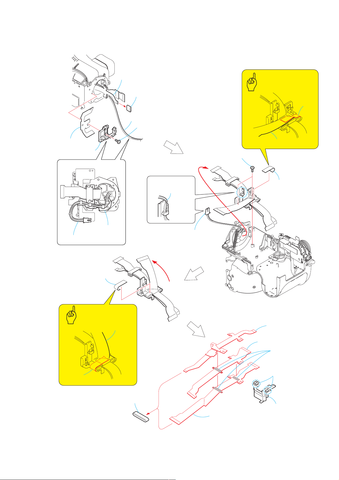
2-21.FP-747/746/754 FLEXIBLE BOARD
FP-754 flexible board
1
Ferrite core
2
harness (PT132)
3
Screw (M1.7 × 3),
lock ace
5
Radiation sheet (LR)
4
Flexible guide (R)
Harness processing
6
Two screws (M1.7 × 3),
lock ace
7
DSC-F828
Caution
Tape (A)
FP-747 flexible board
Flexible guide (R)
Harness (PT-132)
q;
Tape (A)
Caution
FP-747 flexible board
Harness processing
harness (PT132)
8
harness (PT132)
9
Tape (A)
qg
FP-754 flexible board
qh
FP-746 flexible board
Tape (A)
qa
Ferrite core
2-15
qj
FP-747 flexible board
qf
Adhesive tape
qs
Two claws
qd
Flexible guide (L)
Page 23
DSC-F828
2-22.HINGE/CABINET (LL) ASSEMBLY
Hinge /Cabinet (LL) Assembly
1
Rotate the Hinge/Cabinet (LL) Assembly up to the position
where screw becomes visible.
Remove it while rotating the Hinge/Cabinet (LL) Assembly.
3
4
2
Two screws(2 × 4),
lock ace
2-23.SPEAKER/MICROPHONE SECTION
1
Three screws (M1.7 × 3),
2
Speaker /Microphone
section
lock ace
8
Speaker
retainer plate
6
Tapping screw
(M1.7
×
Harness processing
Speaker
Microphone holder
9
7
4)
Claw
Speaker
4
Microphone
5
Microphone
Microphone gom
2-16
3
Microphone grille
Page 24
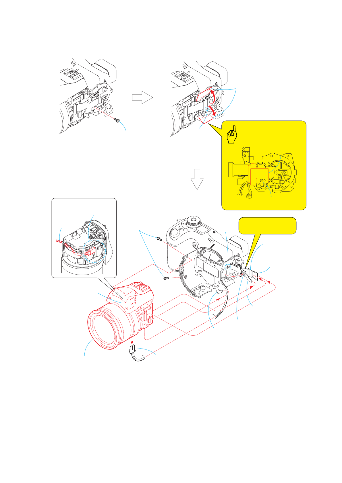
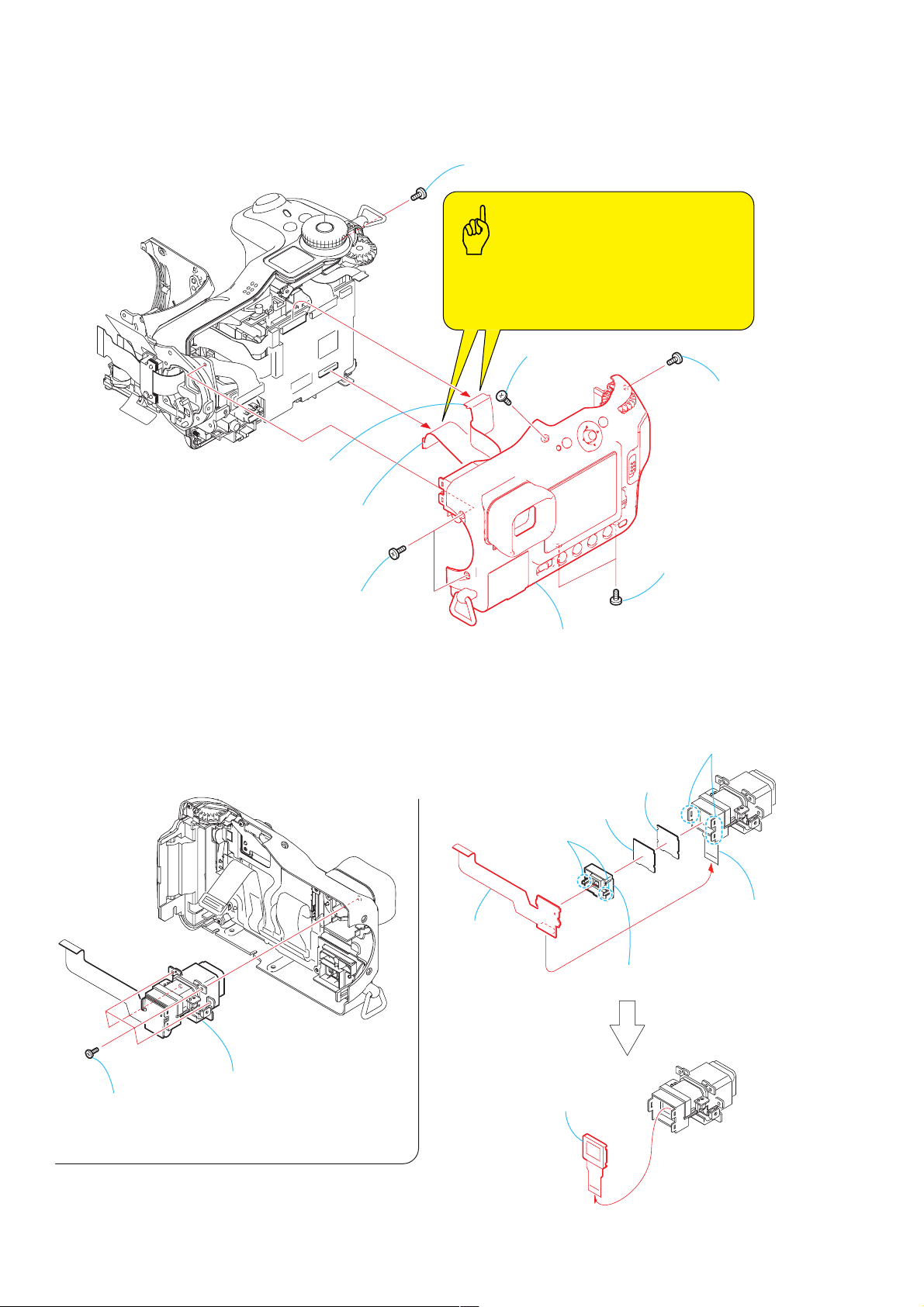
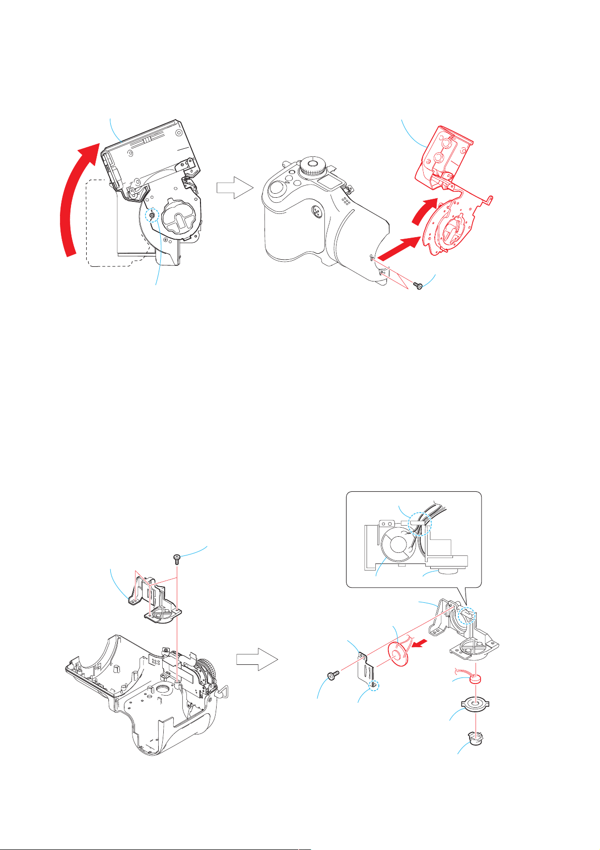
2-24.CABINET UPPER ASSEMBLY
2
Notch
DSC-F828
4
Three tapping screws (M1.7 × 4)
5
Control switch block (top),
LCD module section
1
Two screws (M1.7 × 3),
lock ace
3
Cabinet upper section
Control switch block (top)
Caution
When installing it, align the switch position
as shown.
6
MD cushion
7
Cabinet upper assembly
2-17
Page 25

DSC-F828
[SERVICE POSITION (SY-096 BOARD) ]
FP-749 flexible board (10P)
Memory stick connector
FP-746 flexible board (51P)
FP-747 flexible board
(51P)
ST-088 board
CN502
CN402
FP-756 flexible board
(51P)
CN711
CN702
FP-754 flexible board (21P)
CN706
CN701
CN709
CN751
CN707
Control switch block (top) (12P)
CN451
SY-096 board
Control switch block (under) (50P)
CN703
CN401
CN103
CD-469 board
CN404
harness (2P)
(PT-132)
FP-751 flexible board
Caution
Note: High-voltage cautions.
DD-204 board
CN401
CN001
CN601
DC-IN connector
Extension cable
(6P)
UA-003 board
CN001
SW-410 board
DC-IN
AC power
adaptor
PROCEDURE OF REMOVING THE SY-096 BOARD (SERVICE POSITION)
1 2-1. CABINET (LR) ASSEMBLY, SW-410 BOARD ................................
2 2-2. STROBOSCOPE BLOCK ASSEMBLY ...........................................
3 2-9. REAR CABINET BLOCK ASSEMBLY ...........................................
4 2-13. BTH SECTION ..............................................................................
5 2-14. SY-096 BOARD .............................................................................
6 2-15. DD-204 BOARD ............................................................................
7 2-16. CF-097 BOARD ............................................................................
8 2-18. MEMORY STICK CONNECTOR ..................................................
9 2-20. DC-IN CONNECTOR,UA-003 BOARD .........................................
q; 2-21. FP-747/746/754 FLEXIBLE BOARD ............................................
qa 2-24. CABINET UPPER ASSEMBLY .....................................................
(page 2-2)
(page 2-3)
(page 2-8)
(page 2-10)
(page 2-11)
(page 2-12)
(page 2-12)
(page 2-13)
(page 2-14)
(page 2-15)
(page 2-17)
AC IN
2-18
Page 26

2-25.CONTROL SWITCH BLOCK (TOP)
3
LCD panel
2
Two claws
DSC-F828
4
Control switch block (top)
1
Tape (A)
Caution
Tape (A)
Control switch block (top)
2-19
Page 27

DSC-F828
2-26.CIRCUIT BOARDS LOCATION
ST-088
CF-097
DD-204
SY-096
UA-003
Board Name Function
SY-096
UA-003
SW-410
AJ-007
ST-088
CF-097
CAMERA DSP, CAMERA SYSTEM CONTROL, CF DRIVE I/F, USB I/F, MODE CONTROL,
AUDIO AMP, LCD DRIVER, EVF, LCD DRIVER, CONNECTOR, POWER SUPPLY
AV, USB JACK
FUNCTION KEY
JACK
FLASH CONTROL
CF CARD CONNECTOR
SW-410
AJ-007
DD-204
DC/DC CONVERTER
2-20
Page 28

2-27.CIRCUIT BOARDS AND FLEXIBLE BOARDS LOCATION
Control switch block (top)
Control switch block (under)
FP-749
(flexible)
SI-037
LR-018
DSC-F828
FP-748
MT-067
FP-754
(flexible)
AJ-006
(flexible)
Control switch block (mid)
FP-746
(flexible)
FP-751
(flexible)
FP-756
(flexible)
LB-091
LS-067
FP-747
(flexible)
FP-750
(flexible)
Board Name Function
SI-037
MT-067
LS-067
LB-091
FP-748
LR-018
FLASH, IR LED
FLASH MOTOR
AF LASER
EVF, EVF BACK LIGHT
CONNECTOR
BATTERY, RESET SW
2-21E
Page 29

DSC-F828
)
2003. 12. 8 Update
HELP
Sheet attachment positions and procedures of processing the flexible boards/harnesses are shown.
CABINET (LR) SECTION
Tape (A)
SW-410 board
FP-751 flexible board
FRONT CABINET SECTION
FP-747 flexible board
Tape (A)
FP-747 flexible board
STROBOSCOPE SECTION
Tape (A)
Control switch block (top)
FP-747 flexible board
FP-746 flexible board
Radiation sheet (LR
Tape (A)
FP-754 flexible board
Tapping screw
(M1.7
×
4)
Radiation sheet (LL)
AJ-007 board
REAR CABINET SECTION
Control switch block (under)
Tape (A)
Tape (A)
Block light guide plate
HELP
Page 30

DSC-F828
BTH SECTION
CF radiation sheet (B)
BT holder assembly (front side)
DD-204 board
Fuse replacement caution label
CF radiation sheet (A)
BT holder assembly (rear side)
Sheet (MS)
Memory stick connector
SY-096 board
Cushion (SY)
Tape (A)
Ferrite bead
FP-749 flexible board
HELP
Page 31

Link
Link
DSC-F828
3. BLOCK DIAGRAMS
OVERALL BLOCK DIAGRAM (1/3)
OVERALL BLOCK DIAGRAM (1/3)
OVERALL BLOCK DIAGRAM (2/3) POWER BLOCK DIAGRAM (2/2)
OVERALL BLOCK DIAGRAM (2/3) POWER BLOCK DIAGRAM (2/2)
OVERALL BLOCK DIAGRAM (3/3)
OVERALL BLOCK DIAGRAM (3/3)
POWER BLOCK DIAGRAM (1/2)
POWER BLOCK DIAGRAM (1/2)
Page 32

DSC-F828
BLOCK DIAGRAMS
3-1. OVERALL BLOCK DIAGRAM (1/3)
LENS UNIT (1/3)
IRIS
SHUTER
IRIS
MOTOR
M
SHUTTER
MOTOR
M
FOCUS
MOTOR
M
IR FILTER
MOTOR
M
IRIS RESET
SENSOR
FOCUS RESET
SENSOR
IR FILTER
SENSOR
ZOOM RING
POSITION
SENSOR
FOCUS
RING
FG
20
13
24
21
39
36
10
32
34
27
5
8
1
3
IRIS A
IRIS A
IRIS B
IRIS B
SHUTTER +
SHUTTER -
FOCUS A
FOCUS A
FOCUS B
FOCUS B
IR +
IR -
FC RING FG A
FC RING FG B
V1A,B,C
V2
V3A,B,C
V4
V5A,B,C
V6
RG
12-13
17
C3-C7
B4-B8,A7
G4
H4
G5
H6
E7
D7
A6
B5
A4
B4
C1
D2
TIMING
GENERATOR
28,27,23
20,19
H8-H6,H4
G5,G3
IRIS DRIVE
FOCUS MOTOR
H1A,B,C
H2A,B,C
SHUTTER
DRIVE
DRIVE
IR FILTER
DRIVE
BUFFER
V OUT
MCK TG
E7
ADCLK
E6
TGCLK
D9
SHD
F5
SHP
F6
XCAM RST
D1
E2
F2
CAM HD
E1
CAM F
F1
FP-746
FLEXIBLE(2/6)
G1
34
G2
33
H2
35
G3
FP-747 FLEXIBLE
(2/6)
F7
28 24
F8
41 11
C8
37
C7
36
B8
38
B7
29
B3
40
A2
43 9
45 7
42 10
41
46 6
FP-746
FLEXIBLE
(3/6)
30
29
FP-747
FLEXIBLE
(3/6)
MIC901
SP901
SPEAKER
SECTION 3
3. BLOCK DIAGRAMS
3. BLOCK DIAGRAMS
( ) : Number in parenthesis ( ) indicates the division number of schematic diagram where the component is located.
SY-096 BOARD (1/3)
18
5
21 1
3 19
1 21
31
30
HR EN3
HR DIR3A
HR DIR3B
MSHUT EN
MSHUT DIR
HR EN2
HR DIR2A
HR DIR2B
IR FILTEREN EN
IR FILTEREN DIR
XFC RST SENS
XIR RST SENS
HOT STRB ON
EXT STRB ON
STRB ON
IR LED ON
PANEL R
PANEL G
PANEL B
HDO
PANEL V
IC303
VIDEO AMP
FP-754
FLEXIBLE
FP-746
FLEXIBLE
(1/6)
6
4
Q302-Q304
BUFFER
(1/10)
HJ J2J4 G5
CAM SO,SCK
8127
44 40 45
XCAM RST
HR EN3
HR DIR3A
HR DIR3B
MSHUT EN
MSHUT DIR
HR EN2
HR DIR2A
HR DIR2B
IR FILTEREN EN
IR FILTEREN DIR
IRIS RESET SENS AD
XFC RST SENS
XIR RST SENS
ZOOM POS OUT
CCDINP
CCDINM
C1
B1
CAM SO,S1,SCKCAM SO,SCK
FP-747
FLEXIBLE(1/6)
CN702
S/H,AGCCCD IMAGER
A815
J3F1
C9 B9
CAM F
MCK TG
CAM HD
SHD,SHP
XCAM RST
9
43
CN701
18
19
17
CN702
15
16
14
13
12
CN701
CN702
22
23
CN712
CN713
MIC IN
1
SP+
1
SP-
2
MIC
A/D CONV.
F9
E9
ADCLK
3
EEPROM
4
2
1
J8J5
CLP OB
1
3
TO
OVER ALL
BLOCK DIAGRAM
(2/3)
(PAGE 3-3)
V OUT
A2,B1,J2,
(C,D,E,F,
G) (1,3)
(1/10)
IC304
FC RING
FG AMP
CAM AD0
CAM AD13
CLP OB
MCK TG
TG CLK
CA HD
CA F
(AA,AB,Y)
(13-17)
Y18
AC16
AC20
Y17
AB18
N21
L21
P21
AA5
U21
M21
H20
N20
W21
Y21
F21
Y21
H21
U20
AA4
AB3
AB4
U20
E23
C23
D23
C18
D17
F23
XSYS RST
IC301
CAMERA
T20
4
17
CN711
21
22
CN701
42
(1/10)
(AA,AB,AC,
MC D0-D15 MC D0-D15 CF D0-D15
U,V,W,Y)
(1-4)
(J,K,L,M,
MC A1-A25 MC A0-A10,A24MC A0-A25
N,P,R,T,U)
(1-4)
MC CKIO
T23
AU LRCK
AA7
DSP
HR DQ00
HR DQ31
HR AQ00
HR AQ12
HR QCLK
AU A IN
AU A OUT
(A-E,
L-M,
P,R)
(1-3,
7-9)
(F-J)
(1-3,
7-9)
J1
CAM SO,SI,SCK
(A-G)
(1-4),
(A-D)
(13-17)
(B,C,D),
(4-8)
AC12
A4,
B8
AC9
(1/10)
IC302
SRRAM
512Mbit
XCAM RST
IRIS RESET SENS AD
ZOOM POS OUT
X501
27MHz
MC D0-D15
(H,J,K,L,
M,N)
(23-26)
A8
K1
A10
D8
G26
E4
E4
A17
D16
B15
(2/10)
IC501
CAMERA
SYSTEM
CONTROL
(AA,AB,N,
P,R,T-W,Y)
(23-26)
(3/10)
IC452
MICRO
DRIVE
(H,J,K,
I/F
L,M)
(8-10)
B9,D12,
(E,F,G)
(1-3),H11
MC CKI0
A11
XSYS RST
C7
C19
C22
B20
MS SDIO/DATA0-3,MS BS, MS SCLK
B21
D21
C11
B17
FR SO,SI,SCK
B16
M2
XSYS RST
D14
XACCESS LED
E26
XCF COVER OPEN
AC19
XPROGRAM DIAL A
AC15
XPROGRAM DIAL B
AE14
XMINL LCD BL ON
C7
XAE LOCK ON
AE12
XSHTR ON
AD11
STRB CHG
AE17
XSTRB FULL
AD13
EXT STRB CONT
AD18
STRB POP UP CNTSENS
D24
C17
A16
SYS SO,SI,SCK
D15
PRELAMP AF ON
AC14
PRELAMP AF CONT
A2
PD LV
D5
SELF TIMER LED
H25
XSTRB POP UP
AE13
STRB POP UP DC EN
STRB POP UP DC DIR
A7
STRB POP UP DC BRAKE
A16
B6
(AA,AB,AC,
PHY DATA0-DATA15 USBPHY D+,D-
T,U,W,Y)
(1-4)
PHY CLKOUT
N1
PHY RESET
AC3
MELODY
AD12
MELODY EW
AF14
2
3
50
29
IC251
55 11
28
Q601
BEEP
MOD
AU A IN
AU A OUT
MIC IN
SP+
SP-
TO
OVER ALL
BLOCK DIAGRAM
(3/3)
(PAGE 3-6)
TO
OVER ALL
BLOCK DIAGRAM
(2/3)
(PAGE 3-3)
(4/10)
USB2.0
I/F
E1
H4
H5
B9
A2
D1
(A-F)
(1-4)
(F,G,H
J,K,L)
(1-3)
M7
12
(6/10)
IC601
AUDIO
AMP
FP-756
CF-097 BOARD
FLEXIBLE
CN101
48
48
41
41
12
12
3
3
39
39
33
33
31
31
15
15
32
32
CN103
COMPACT FLASH
MICRO DRIVE
CF A0-A10
CF RESET
CN451
4
4
11
11
40
40
49
49
13
13
19
19
21
21
37
37
20
20
FP-749
CN706
9
3
FLEXIBLE
MEMORY
STICK
CONNECTOR
UA-003 BOARD
CX251
12MHz
CN707
11
10
5
B4
5
A OUT
5
4
CN001
(USB)
A/V OUT (MONO)
J001
3-1 3-2
AUDIO SIGNAL
VIDEO SIGNAL
VIDEO/AUDIO SIGNAL
Page 33

DSC-F828
3. BLOCK DIAGRAMS
3. BLOCK DIAGRAMS
3-2. OVERALL BLOCK DIAGRAM (2/3)
SY-096 BOARD (2/3)
TO
OVER ALL
4
3
1
BLOCK DIAGRAM
(3/3)
(PAGE 3-5)
TO
OVER ALL
BLOCK DIAGRAM
(1/3)
(PAGE 3-2)
TO
OVER ALL
BLOCK DIAGRAM
(1/3)
(PAGE 3-1)
VIDEO SIGNAL
LANC SIG
EXT STRB CONT
STRB POPUP CNTSENS
SYS SO,SI,SCK
PANELAMP AF ON
PANELAMP AF CONT
PD LV
SELF TIMER LED
XSTRB POPUP
STRB POPUP DC EN
STRB POPUP DC DIR
STRB POPUP DC BRAKE
HOT STRB ON
EXT STRB ON
STRB ON
IR LED ON
PANEL R
PANEL G
PANEL B
HDO
PANEL V
PANEL R
PANEL G
PANEL B
HDO
PANEL V
SYS SO,SI,SCK
PANEL R
PANEL G
PANEL B
HDO
PANEL V
SYS SO,SI,SCK
40
39
38
43
42
47
48
46
40
39
38
43
42
47
48
46
( ) : Number in parenthesis ( ) indicates the division number of schematic diagram where the component is located.
2
6
AJ-006
FLEXIBLE
AJ-007 BOARD
CN201
LANC SIG
2
ACC STRB ON
6
LENS UNIT (2/3)
ST-088
BOARD
CN501
22
19
7
15
4
11
12
13
18
17
8
9
LCD901
2.5INCH
LCD
UNIT
BACK LIGHT
ND901
LCD902
COLOR
EVF
UNIT
D504
FLASH
DRIVE
LD OUT
PD OUT
SELF TIMER LED
Q501
LED DRIVE
IC502
Q502-504
FLASH
DRIVE
(7/10)
IC801
RGB DRVE
TIMING
GENERATOR
(LCD)
(8/10)
IC902
RGB DRVE
TIMING
GENERATOR
(EVF)
IC703
(9/10)
IC701
BL UNREG
42
IC702
42
19
20
21
25
35
32
16
6
2
31
28
19
20
21
23
35
31
15
14
4
2
16
28
42
(9/10)
BL ON
BL LEVEL
DC1
EXTDA
(9/10)
STRB POPUO DC EN
STRB POPUO DC DIR
STRB POPUO DC BRAKE
HOT STRB ON
EXT STRB ON
STRB ON
VR
VG
VB
VCOM
HCNT,
MVLK,
OE,
GRES,
STBYB,
SRT,
GSRT,GPCK,CP
(7/10)
IC802
BL
REG
R
G
B
COM
PCG
VST
VCK
STB
EN
DWN
HST
HCK2,HCK1
Q901-903
BACK LIGHT
DRIVE
FP-747
CN702
FLEXIBLE(4/6)
11
9
12
39
8
CN701
FP-746 FLEXIBLE(4/6)
29 23
CN702
26
FP-747
FLEXIBLE(5/6)
27
25
30
31
15
CN701
26 26
FP-746 FLEXIBLE(5/6)
CN702
28
29
FP-747
FLEXIBLE(6/6)
CN703
29
21
25
1
17
13
9
24
5
7
20
22
26
30
CN901
15
16
14
17
3
12
21
41
43
40
13
44
26
25
27
22
21
37
24
23
B2
A1
F2
4
2
CONTROL SWITCH
BLOCK(UNDER) (1/2)
CN002
30
22
26
2
18
14
10
23
6
8
19
21
25
29
LB-091 BOARD
D001
BACK LIGHT
CAM -7.5V
LED DRIVE
STROB
POPUP
MOTOR
DRIVE
AF LD
DRIVE
BL H BLREG
FP-750
FLEXIBLE
1
E1
E2
4
16
8
19
12
11
5
1
10
5
6
15
14
CN001
10
8
9
1
7
3
24
21
CN004
1
CN001
4
3
5
1
16
7
MT-067
BOARD
CN503
1
4
MOTOR POSITION
16
5
8
9
11
CN504
3
4
1
6
CN505
2
6
9
13
14
23
26
SI-037 BOARD
CN502
2
DC 300V
J201
ACC
(Accessory)
STRB POPUP+
STRB POPUP-
S001
DETECT
EXT STRB ON CN
LANC SIG
HOT
D001
AF LASER UNIT
LS-067
BOARD
D004
Self-timer
S001
FLASH
OPEN DETECT
Infrared ray emitter
XE-H
L001
TRIGGER
TRANSFORMER
XE-L
TO
OVER ALL
5
BLOCK DIAGRAM
(3/3)
(DD-204)
(PAGE 3-5)
D001
CN001
10
7
6
4
M910
FLASH
M
MOTOR
AS-050
FLEXIBLE
XENON
TUBE
ACCESSORY
SHOE
3-3 3-4
Page 34

3. BLOCK DIAGRAMS
3. BLOCK DIAGRAMS
DSC-F828
3-3. OVERALL BLOCK DIAGRAM (3/3)
SW-410 BOARD
S001-007
OPEN(FLASH),FLASH,
METERING MODE,MACRO,
BURST/BRACKET,FOCUS,
NIGHT SHOT/NIGHT FLAMING
(8/10)
IC201
12
LCD
37
DRIVE
XRST SW
5
VL 3V
3
BATT SIG
BATT/XEXT
FAST CHARGE
BATT UNREG
D001
50
48
51
38
27
28
LANC SO
LANC SIG LANC SIG
SYS DD ON
DDCON SO,SCK
DD 1.8V
DD P5V
DD 2.95V
DD 4.7V
DD 3.3V
DD 4.2V
DD 15V
DD -7.5V
ACV UNREG
BL UNREG
STRB CHG
XSTRB FULL
C405
(FLASH)
BT901
BATTERY
TERMINAL
J901
DC IN
LR-018
BOARD
DD-204 BOARD
CN002
1
2
S
3
CN001
1
2
3
LCD903
CHARACTER
DISPLAY
UNIT
Q001,002
1
25
S001
RESET
STRB UNREG
CN201
COMO-COM3,SEG1-SEG20
BT001
LITHIUM
BATTERY
(SECONDARY)
IC001
DC/DC
CONVERTER
IC004
LANC
I/O
HI VOLTAGE
CHARGER
Q401,402,407
( ) : Number in parenthesis ( ) indicates the division number of schematic diagram where the component is located.
SY-096 BOARD (3/3)
KEY AD3
24
KEY AD4
25
CN701
IC402
3V
REG
EVER 3.0V
(5/10)
8
4
RESET
TO
OVER ALL
BLOCK DIAGRAM
(2/3)
(PAGE 3-3)
32.768KHz
6
X401
J7
KEY AD3
H7
KEY AD4
C1D3DDCON SO
DDCON SCK
32KHz IN
J4
32KHz OUT
J5
XRSTX
D75
A5
BACK UP VCC
H4
BATT SIG
F1
BATT/XEXT
A7
FAST CHARGE
H2
SYS DD ON
E8
LANC SO
F2
LANC SI
F3
(5/10)
IC401
HI CONTROL
XCHARGE/
XSTRB LED
KEY AD 0
KEY AD 1
KEY AD 2
MODE DIAL 0
MODE DIAL 1
XPOWER LED ON
XPWR ON
FR SO
FR SI
XFR SCK
LED DRIVE
LED DRIVE
FR SO,SI,SCK
XSYS RST
XACCESS LED
XCF COVER OPEN
XPROGRAM DIAL A
XPROGRAM DIAL B
XMINI LCD BL ON
XAE LOCK ON
XSHTR ON
STRB CHG
XSTRB FULL
Q701
Q704
2
XACCESS LED
B1
J6
H6
G6
J8
J9
XMINI LCD
BL ON
B2
B8
D2
D1
E1
B3XSYS RST
RST VIN
LANC SI
CN001
CN601
CN401
2
3
9
8
33
35
25
27
29
37
9
11
7
23
19
17
15
13
1
FP-751
FLEXIBLE
FP-748
FLEXIBLE
33
35
25
27
29
37
9
11
7
23
19
17
15
13
DC300V
CN751CN602
LENS UNIT
(3/3)
2
3
DDCON SO,SCK
5
TO
OVER ALL
BLOCK DIAGRAM
(2/3)
(ST-088)
(PAGE 3-4)
28
27
FP-746
FLEXIBLE
(6/6)
VL 3V
RST VIN
3
7
TO
OVER ALL
BLOCK DIAGRAM
(1/3)
(PAGE 3-2)
CN703
XCHARGE/XSTRB LED
XCF COVER OPEN
XPROGRAM DIAL A
XPROGRAM DIAL B
KEY AD0 GUI DOWN
KEY AD1
KEY AD2
KEY AD0 L5
CN709
KEY AD0 L2
MODE DIAL 0
MODE DIAL 1
XPWR ON
XAE LOCK ON
XACCESS LED
CONTROL SWITCH
BLOCK(UNDER)
CN002
17
18
49
50
35
36
39
40
37
38
45
46
GUI UP
41
42
43
44
9
10
1
2
10
9
8
X MINI LCD BL ON
12
2
3
5
6
CONTROL SWITCH
BLOCK(TOP)
D001
ACCESS
S001-006
FINDER/LCD,SCREEN STATUS,
SELF TIMER/INDEX,
DIGITAL ZOOM,QUICK REVIEW,
MEMORY STICK/CF CARD
S003-005
WHITE BALANCE,
EXPOSURE,
DISPLAY WINDOW BACKLIGHT
MINI LCD BACK LIGHT
D001
POWER
POWER
SHUTTER
D006
S002
S001
MODE
DIAL
CN003
1
9
7
8
3
5
4
CONTROL SWITCH
BLOCK(MID)
D001
FLASH
CF COVER OPEN
COMMAND
DIAL
MULTI-
SELECTOR
MENU,
S002,S012
AE LOCK
3-5 3-6
Page 35

DSC-F828
3. BLOCK DIAGRAMS
3. BLOCK DIAGRAMS
3-4. POWER BLOCK DIAGRAM (1/2)
DD-204 BOARD
CN002
BATT UNREG
1
BATT SIG
2
S
3
CN001
AV UNREG
1
2
BATT/XEXT
3
27 25 29 31
27
CN002
27 25 29 31
27
CN751
(5/10)
IC402
5 D7
RESET
DETECT
6
4 A9
S001
RESET
BATTER IN
8
EVER 3.0V
39 33
39 33
EVER 3.0V
BT001
LITHIUM
BATTERY
(SECONDARY)
Q001,002
25 29 31
25 29 31
H8 BATT SENS
G8 ACV SENS
F1 BATT SIG
A7 BATT/XEXT
J4 INIT CHARGE
H2 FAST CHARGE
A5
H4
B8
F8
CN751
CN002
CN001
CN601
CN602
CONTROL
SWITCH
BLOCK
(TOP)
POWER
POWER
D001
SY-096 BOARD (1/3)
S002
CN709
3
1
BT901
BATTERY
TERMINAL
J901
DC IN
D404
2
VCH
3
3V
7
REG
35 39 33
35
35 39 33
35
VL 3V XRST SW
35
( ) : Number in parenthesis ( ) indicates the division number of schematic diagram where the component is located.
Q007
SWITCHING
Q008
SWITCHING
Q009
SWITCHING
Q010
SWITCHING
Q011
Q012
SWITCHING
Q401,402,407,T401
HIGHT VOLTAGE
CHARGER
L002
L003
L004 L759
L005
L006
L007
Q015
SWITCHING
2
D011
RECT
D010
RECT
IC004
C405
L011
-7.5V
REG
XRSTX
BACK UP VCC
BATT IN
XPER ON
DDCON SENS
CHARGE
SWITCH
(5/10)
IC401
HI CONTROL
Q003,004
CN601
CN001
C1
DDCON SCK
D3
DDCON SCK
H1
XCS DD CON
38CTL1
XLANC IC ON
A1
FP-748 BOARD(1/2)
F001
STRB UNREG
F005
BATT UNREG
F004
UNREG3
F006
5V UNREG
F003
BL UNREG
F002LF001
ACV UNREG
RST VIN
37
37
BATT UNREG
45
45
ACV UNREG
43
43
19
19
17
17
21
21
23
23
3
3
CN751 CN002 CN001 CN601
37
45
43
19
17
21
23
3
37
45
43
19
17
21
23
3
D001
DDCON SO,SCK,XCS
Q006
37
VREF
30
OUT1
OUT2
OUT3
-INE7
RT
57
20IN1
58
21
IN2
59
22IN3
60OUT4
23IN4
SWITCHING
61OUT5
24IN5
62OUT6
25IN6
L001
63OUT7
2
IC001
DC/DC CONVERTER
LANC I/O
56
VCC
43
VIN
27
DIN
28
CLK
26
LD
38 CTL1
XCTL 2
47
5.6V
52
REG
54
29 RST
V CONT
LANC DC
LANC
I/O
STRB CHG
XSTRB FULL
BL UNREG
DD 1.8V
DD P 5V
DD 2.95V
DD 4.7V
MD 3.3V
DD 4.2V
DD 15.5V
DD -7.5V
1
CN401
1
15
15
13
13
41
41
49
49
36
36
38
38
40
40
42
42
44
44
46
46
48
48
50
50
52
52
53
53
54
54
56
56
58
58
60
60
55
55
57
57
59
59
47
47
51
51
FP-748
BOARD
(2/2)
DC 300V
TO
POWER BLOCK DIAGRAM (2/2)
1
(PAGE 3-10)
SY-096 BOARD (2/3)
15
15
13
13
41
41
L757
49
49
36
36
38
38
40
40
42
42
44
44
46
46
48
48
50
50
L760
52
52
L761
L751
53
53
L753
54
54
56
56
58
58
60
60
55
55
L756
57
57
59
59
47
47
51
51
MD 3.3V
STRB CHG
XSTRB FULL
BL UNREG
PANEL 13.5V
PANEL 2.95V
PANEL 4.7V
D 1.8V
(10/10)
IC751
1
3
L763
1.2V REG
(10/10)
IC752
3.3V
REG
Q752
13.5V REG
(10/10)
IC753
15.1V
REG
,Q751
D 1.2V
CAM P 5V
PANEL 2.95V
D 2.95V
A 2.95V
PANEL 4.7V
L754
CAM 3.3V
5
MD 3.3V
TG 4.2V
PANEL 13.5V
CAM 15V
12
CAM -7.5V
EVER 3.0V
CAM 15V
CAM P 5V
D 2.95V
D 1.2V
D 1.8V
A 2.95V
CAM 3.3V
TG 4.2V
CAM -7.5V
2
TO
POWER
BLOCK DIAGRAM
(2/2)
(PAGE 3-9)
LANC DC
5
LR-018 BOARD
5
CN601 CN001 CN002 CN751
5
5
3-7 3-8
D 1.2V
EVER 3.0V
LANC DC
Page 36

3. BLOCK DIAGRAMS
3. BLOCK DIAGRAMS
DSC-F828
3-5. POWER BLOCK DIAGRAM (2/2)
SY-096 BOARD (3/3)
(3/10)
IC451
OR
GATE
L452
(3/10)
IC452
MICRO
DRIVE
I/F
FB901
(8/10)
IC902
RGB DRIVE
TIMING
GENERATOR
L902
(6/10)
IC601
AUDIO
AMP
2
TO
POWER
BLOCK DIAGRAM
(1/2)
(PAGE 3-8)
MD 3.3V
STRB CHG
XSTRB FULL
BL UNREG
PANEL 13.5V
PANEL 2.95V
PANEL 4.7V
EVER 3.0V
CAM 15V
CAM P 5V
D 2.95V
D 1.2V
D 1.8V
A 2.95V
CAM 3.3V
TG 4.2V
CAM -7.5V
LANC DC
D 2.95V
PANEL 13.5V
PANEL 2.95V
PANEL 4.7V EVF LED A
( ) : Number in parenthesis ( ) indicates the division number of schematic diagram where the component is located.
FP-756
FLEXIBLE
K6
Q451
CF POWER ON
CN451
25
25
28
28
CN901 CN001
1
CN101 CN706
27
27
24
VCC
24
CF-097
BOARD
VDD
LB-091
BOARD
D001
(4/10)
IC251
USB 2.0
I/F
BACK LIGHT
(9/10)
IC701
IC702
IC703
BUFFER
19
(1/10)
IC304
FC RING
FG AMP
(1/10)
IC301
CAMERA
DSP
L602
AU 2.95V
FB301
(1/10)
IC303
VIDEO
AMP
(1/10)
IC302
SDRAM
512Mbit
XFC RST LED
U22
XIRIS RST LED
V22
XIR SENS LED
T22
XMF SENS LED
W20
COMPACT FLASH/
18
CN103
MICRO DRIVE
LCD902
COLOR
EVF
UNIT
(8/10)
IC201
DRIVE
24
XCSSAVE2
1
3
EVER 3.0V
Q702
2
CN703 CN001
33
49
Q801,802
35
47
45
Q703
34
30
D805
(RECT)
28
48
R701
CN701
42
CAM P 5V
39
D 2.95V
MS PWR ON
PANEL 4.7V
PANEL 2.95V
CAM 15V
PANEL 13.5V
BL MODE
BL UNREG
BL ON
BL LEVEL
L804
L803
(7/10)
IC801
RGB
DRIVE
31
TIMING
GENERATOR
28
L806L805
(7/10)
6
5
IC802
9
BL REG
FP-746
FLEXIBLE
D 2.95V
CAM 15V
LANC DC
CN702
(1/2)
38
37
8
32
31
21
19
18
33
17
LCD
L581
L582
L583
L584
AVDD PLL 1.2V
AVDD AD 2.95V
AVDD DA 2.95V
AVRT DA 2.95V
(2/10)
IC501
CAMERA
SYSTEM
CONTROL
STRB CHG
AE17
XSTRB FULL
AD13
MS PWR ON
AC18
BL MODE
E25
CAM DD ON
AE19
XMF SENS LED
CAM -7.5V
XFC RST LED
XIRIS RST LED
XIR SENS LED
CAM DD ON
FP-747
FLEXIBLE
CN701
36
A 2.95V
35
34
CAM 3.3V
33
45
TG 4.2V
43
FP-746
FLEXIBLE
(2/2)
FP-749
FLEXIBLE
CN002
34
50
36
48
46
27
33
31
47
10
13
14
15
44
20
21
31
33
34
19
35
16
17
18
19
7
9
VCC
VSH (5V)
VDD (3V)
VGH (15V)
VDC (15V)
CONTROL
SWITCH
BLOCK
(UNDER)
BL THH
BL H BL REG
BL L IN2-
IRIS/
SHUTTER/
FOCUS/
IR FILTER
DRIVE
EEPROM
A/D
CONV.
CN004
CN003
11
12
20
19
18
6
1
3
2
MEMORY
STICK
CONNECTOR
LCD901
2.5INCH
BACK LIGHT
UNIT
LCD
ND901
THERMISTOR
FLASH
CONTROL SWITCH
D001
BLOCK (MID)
AF LD
DRIVE
BUFFER
S/H
AGC
17
18
FP-750
FLEXIBLE
XMF SENS LED
XFC RST LED
XIRIS RST LED
XIR SENS LED
CAM DD ON
3 5
CN501
6
5
ST-088 BOARD
3.45V
REG
Q502-504
FLASH
DRIVE
ZOOM POSI VCC
MF VCC
F SENS VCC
IRIS SENS VCC
IR SENS VCC
3.45V
CN502
R509,510
28
29
31
11
12
35
TO
POWER BLOCK DIAGRAM (1/2)
1
(DD-204)
2
2
(PAGE 3-8)
CN505
6
9
Infrared ray
1
emitter
ZOOM RING
POSITION
SENSOR
FOCUS
RING
FG
FOCUS
RESET
SENSOR
IRIS
RESET
SENSOR
IR FILTER
RESET
SENSOR
TIMING
GENER
44
AJ-006
FLEXIBLE
D001
SI-037
BOARD
LENS UNIT
CCD
IMAGER
CN201
AJ-007
BOARD
XE H
XENON
TUBE
J201
ACC
(Accessory)
3-9 3-10E
Page 37

SECTION 4
PRINTED WIRING BOARDS AND SCHEMATIC DIAGRAMS
4-1. FRAME SCHEMATIC DIAGRAM (1/4)
4-2. SCHEMATIC DIAGRAMS 4-3. PRINTED WIRING BOARDS
4-2. SCHEMATIC DIAGRAMS 4-3. PRINTED WIRING BOARDS
DSC-F828
1
A
XENON TUBE
25
D001
Infrared ray emitter
B
SI-037 BOARD
C
D
D001
AF LASER UNIT
E
LS-067 BOARD
1
IR_LED_A
2
IR_LED_K
3
N.C.
4
N.C.
5
N.C.
6
XE_H
7
XE_H
8
XE_H
9
XE_H
10
N.C.
11
N.C.
12
N.C.
13
TRIGGER
14
TRIGGER
15
N.C.
16
N.C.
17
N.C.
18
REG_GND
19
REG_GND
20
N.C.
21
N.C.
22
N.C.
23
XE_L
24
XE_L
25
XE_L
26
XE_L
CN504
1
SELF_TIMER_LED
2
REG_GND
3
LD_OUT
4
PD_OUT
5
REG_GND
6
XSTRB_POPUP
463
26PCN505
22PCN501
REG_GND
LANC_SIG
REG_GND
PD_OUT
LD_OUT
STRB_ON
IR_LED_ON
CAM_P_5V
D_2.95V
REG_GND
REG_GND
REG_GND
CN502
REG_GND
DC_300V
22
21
20
19
18
17
16
15
14
13
12
11
10
9
8
7
6
5
4
3
2
1
2P
1
2
STRB_POPUP+
STRB_POPUP+
STRB_POPUP-
STRB_POPUP-
SELF_TIMER_LED
XSTRB_POPUP
ST-088 BOARD
6P
16PCN503
EXT_STRB_ON_CN
XASHOE_JACK_IN
STRB_POPUP_CNTSENS
HOT_STRB_ON
810 137
1
TO
DD-204 BOARD
CN401
(PAGE 4-7)
FP-750
FLEXIBLE
11
1
2
3
4
5
6
7
8
9
10
11
12
13
14
15
16
17
18
19
20
21
22
129
22P
STRB_POPUP+
STRB_POPUP+
STRB_POPUP-
STRB_POPUP-
SELF_TIMER_LED
XSTRB_POPUP
REG_GND
LANC_SIG
REG_GND
PD_OUT
LD_OUT
EXT_STRB_ON_CN
XASHOE_JACK_IN
STRB_ON
IR_LED_ON
STRB_POPUP_CNTSENS
CAM_P_5V
D_2.95V
HOT_STRB_ON
REG_GND
REG_GND
REG_GND
LENS UNIT(1/2)
(CD-469 BOARD)
F
S001
FLASH OPEN
(
DETECT
G
ACCESSORY SHOE
H
)
AS-050
FLEXIBLE
D004
(Self-timer)
LANC_SIG
10
REG_GND
9
8
N.C.
7
HOT
6
HOT
5
N.C.
EXT_STRB_ON_CN
4
3
XASHOE_JACK_IN
2
SHOE_GND
SHOE_GND
1
STRB_POPUP-
LANC_SIG
STRB_POPUP+
STRB_POPUP+
1234567
10PCN001
REG_GND
STRB_POPUP-
HOT
N.C.
8
XASHOE_JACK_IN
N.C.
EXT_STRB_ON_CN
HOT
9
SHOE_GND
10111213141516
STRB_POPUP_CNTSENS
REG_GND
SHOE_GND
SW-410
BOARD
CN001
KEY_AD3
KEY_AD4
REG_GND
6P
1
N.C.
2
FP-751
3
4
N.C.
N.C.
5
6
FLEXIBLE
1
2
3
4
5
6
Note:
Since a servce is not for the single
CD-469 Board.
Because adjustment is needed.
6P
N.C.
KEY_AD3
KEY_AD4
N.C.
REG_GND
N.C.
2
TO
LENS UNIT
(2/2)
(PAGE 4-3)
AJ-007 BOARD
I
M910
J
FLASH MOTOR
S001
MOTOR POSITION
DETECT
MT-067 BOARD
J201
ACC(Accessory)
LANC_GND
LANC_SIG
LANC_GND
LANC_DC
XLANC_JACK_IN
ACC_STRB_ON
6PCN201
1
2
AJ-006
3
4
FLEXIBLE
5
6
1
LANC_GND
2
LANC_SIG
3
LANC_GND
4
LANC_DC
5
XLANC_JACK_IN
6
ACC_STRB_ON
6P
M
16
4-1 4-2
FRAME SCHEMATIC DIAGRAM (1/4)
Page 38

DSC-F828
FRAME SCHEMATIC DIAGRAM (2/4)
4-2. SCHEMATIC DIAGRAMS 4-3. PRINTED WIRING BOARDS
4-2. SCHEMATIC DIAGRAMS 4-3. PRINTED WIRING BOARDS
1
810 137
11
129
144 1763
1825 15 16
A
REG_GND
1
REG_GND
2
REG_GND
3
REG_GND
4
REG_GND
5
XFE_CS
B
C
D
LENS
E
F
G
2
TO
LENS UNIT
(1/2)
H
(PAGE 4-2)
1
MF_OUT_F0
2
MF_VCC
3
MF_OUT_F1
4
MF_GND
5
SHUTTER+
6
SHUTTER+
7
SHUTTER-
8
SHUTTER-
9
IRIS_SENS_GND
10
IRIS_SENS_OUT
11
IRIS_SENS_VCC
12
IRIS_SENS_VCC
13
IRIS_B
14
IRIS_B
15
IRIS_B
16
IRIS_B
17
IRIS_A
18
IRIS_A
19
IRIS_A
20
IRIS_A
21
FOCUS_B
22
FOCUS_A
23
FOCUS_B
24
FOCUS_A
25
STATIC_GND
26
ZOOM_POSI_GND
27
ZOOM_POSI_OUT
28
ZOOM_POSI_VCC
29
ZOOM_POSI_VCC
30
GND(SENS,THERM)
31
F_SENS_VCC
32
F_SENS_OUT
33
THERM_OUT
34
IR_SENS_OUT
35
IR_SENS_VCC
36
IR-
37
IR-
IR+
38
IR+
39
39P
EXT_STRB_CONT
PRELAMP_AF_CONT
LENS UNIT(2/2)
(CD-469 BOARD)
Note:
Since a servce is not for the single
CD-469 Board.
Because adjustment is needed.
51P
21P
EXT_STRB_ON
HOT_STRB_ON
PRELAMP_AF_ON
FC_RING_FGB
FC_RING_FGA
XFC_RST_LED
XCAM_DR_PS
XIRIS_RST_LED
XIR_SENS_LED
XLANC_JACK_IN
SELF_TIMER_LED
XHSHOE_CONT
XLENS_EEP_WE
STRB_POPUP_DC_BRAKE
STRB_POPUP_DC_EN
XLENS_EEP_CS
STRB_POPUP_DC_DIR
STRB_POPUP_CNTSENS
51P
XCAM_SCK
CAM_SO
XCAM_RST
XTG_CS
XCDS_CS
CAM_SI
REG_GND
CCD_TEMP
REG_GND
LENS_TEMP
REG_GND
CAM_DD_ON
MSHUT_REF
STRB_ON
IR_LED_ON
MSHUT_EN
LANC_DC
REG_GND
REG_GND
REG_GND
REG_GND
REG_GND
REG_GND
REG_GND
PD_LV
6
7
8
9
10
11
12
13
14
15
16
17
18
19
20
21
22
23
24
25
FP-747
26
27
28
29
30
31
32
33
34
35
36
37
38
39
40
41
42
43
44
45
46
47
48
49
50
51
FLEXIBLE
5
TO
SY-096 BOARD
(PAGE 4-5)
I
J
16
FRAME SCHEMATIC DIAGRAM (2/4)
3
TO
SY-096 BOARD
(PAGE 4-5)
REG_GND
51
REG_GND
REG_GND
REG_GND
ZOOM_POS_OUT
REG_GND
XFC_RST_SENS
XMF_SENS_LED
IRIS_SENS_AD
IR_FILTER_IN
XIR_RST_SENS
MSHUT_DIR
IR_FILTER_EN
HR_DIR2B
HR_EN2
HR_DIR2A
HR_DIR3B
HR_EN3
HR_DIR3A
FP-746
VSUB_CONT
CA_HD
PBLK
CA_F
KEY_AD3
XSTRB_POPUP
KEY_AD4
FLEXIBLE
XASHOE_JACK_IN
REG_GND
LANC_SIG
CAM_-7.5V
REG_GND
CAM_15V
CAM_3.3V
CAM_3.3V
A_2.95V
A_2.95V
D_2.95V
D_2.95V
CAM_P_5V
CAM_P_5V
CAM_P_5V
CAM_P_5V
1011121314151617181920212223242526272829303132333435363738394041424344454647484950
TG_3.45V
TG_3.45V
TG_3.45V
REG_GND
REG_GND
REG_GND
REG_GND
REG_GND
REG_GND
123456789
CLP_OB
21
AD_GND
AD_GND
CA_AD00
CA_AD01
CA_AD02
FP-754
CA_AD03
CA_AD04
CA_AD05
CA_AD06
CA_AD07
FLEXIBLE
4-3 4-4
CA_AD08
1011121314151617181920
CA_AD09
CA_AD10
CA_AD11
CA_AD12
CA_AD13
AD_GND
MCKTG
AD_GND
TG_CLK
123456789
4
TO
SY-096 BOARD
(PAGE 4-6)
Page 39

FRAME SCHEMATIC DIAGRAM (3/4)
4-2. SCHEMATIC DIAGRAMS 4-3. PRINTED WIRING BOARDS
4-2. SCHEMATIC DIAGRAMS 4-3. PRINTED WIRING BOARDS
DSC-F828
1
7
810 13
9
11
12
1825 15 16
19144 1763
A
12P
CN709
1
EVER_3.0V
XPWR_ON
XAE_LOCK_ON
XSHTR_ON
MODE_DIAL1
MODE_DIAL0
KEY_AD0_L2
CN713
CN712
CN707
USB_GND
USB_D+
USB_GND
USB_VBUS
AV_JACK_IN
CN201
CN706
SDIO/DATA0
USB_D-
A_OUT
V_OUT
SEG10
SEG11
SEG12
SEG13
SEG14
SEG15
SEG16
SEG17
SEG18
SEG19
SEG20
MS_BS
DATA1
DATA2
DATA3
2
3
4
GND
5
6
7
GND
8
9
10
11
GND
12
2P
2SP_-
1SP_+
2P
2MIC_GND
1MIC_IN
12P
12
11
10
9
8
7
6
5
4
UA-003
3
2
BOARD
1
26P
1
COM0
2
COM1
3
SEG0
4
SEG1
5
SEG2
6
SEG3
7
SEG4
8
SEG5
9
SEG6
10
SEG7
11
SEG8
12
SEG9
13
14
15
16
17
18
19
20
21
22
23
24
COM2
25
COM3
26
N.C.
10P
10
VSS
9
8
7
FP-749
6
5
INT
FLEXIBLE
4
3
SCLK
2
VCC
1
VSS
CONTROL SWITCH BLOCK(TOP)
MIC
J001
A/V OUT(MONO)
GND
5
4
ID
3
D+
2
D-
1
VCC
LCD903
CHARACTER DISPLAY UNIT
MEMORY STICK
CONNECTOR
SP901
SPEAKER
MIC901
CN001
(USB)
XPOWER_LED_ON
B
18PCN001
18
VDD
17
VSS
16
RCG
15
C
LCD902
COLOR EVF UNIT
D
VST
14
VCK
13
STB
12
ENB
11
DWN
10
RGT
9
HST
8
HCK2
7
HCK1
6
TEST
5
B
4
R
3
G
2
N.C.
1
COM
LB-091
BOARD
D001
BACK LIGHT
E
F
G
H
5
TO
LENS UNIT(2/2)
(PAGE 4-4)
FP-746
FLEXIBLE
I
J
K
22 N.C.
21 EVF_LED_K
20 N.C.
19 EVF_LED_A
18 N.C.
17 COM
16 G
15 R
14 B
13 TEST
12 HCK1
11 HCK2
10 HST
9 RGT
8 DWN
7 ENB
6 STB
5 VCK
4 VST
3 PCG
2 VSS
1 VDD
REG_GND
51
REG_GND
50
REG_GND
49
REG_GND
48
REG_GND
47
REG_GND
46
TG_4.2V
45
TG_4.2V
44
TG_4.2V
43
CAM_P_5V
42
CAM_P_5V
41
CAM_P_5V
40
CAM_P_5V
39
D_2.95V
38
D_2.95V
37
A_2.95V
36
A_2.95V
35
CAM_3.3V
34
CAM_3.3V
33
CAM_15V
32
CAM_-7.5V
31
REG_GND
30
LANC_SIG
29
REG_GND
28
ASHOE_JACK_IN
27
XSTRB_POPUP
26
KEY_AD4
25
KEY_AD3
24
PBLK
23
CA_F
22
CA_HD
21
VSUB_CONT
20
HR_DIR3A
19
HR_EN3
18
HR_DIR3B
17
HR_DIR2A
16
HR_EN2
15
HR_DIR2B
14
IR_FILTER_EN
13
IR_FILTER_IN
12
MSHUT_DIR
11
XIR_RST_SENS
10
IRIS_RESET_SENS_AD
9
XMF_SENS_LED
8
XFC_RST_SENS
7
ZOOM_POS_OUT
6
REG_GND
5
REG_GND
4
REG_GND
3
REG_GND
2
REG_GND
1
CN701
22PCN901
XMINILCD_BL_ON
SY-096 BOARD(1/2)
51P
CN702
51P
21PCN711
GND_GUARD(REG_GND)
GND_GUARD(REG_GND)
GND_GUARD(REG_GND)
GND_GUARD(REG_GND)
L
REG_GND
REG_GND
REG_GND
REG_GND
REG_GND
XFE_CS
XCAM_SCK
CAM_SO
XCAM_RST
XTG_CS
XCDS_CS
EXT_STRB_CONT
CAM_SI
REG_GND
CCD_TEMP
373839404142434445464748495051
REG_GND
36
REG_GND
LENS_TEMP
MSHUT_REF
CAM_DD_ON
PRELAMP_AF_CONT
PD_LV
STRB_ON
IR_LED_ON
EXT_STRB_ON
HOT_STRB_ON
PRELAMP_AF_ON
MSHUT_EN
FC_RING_FGB
23242526272829303132333435
FC_RING_FGA
XFC_RST_LED
XCAM_DR_PS
XIRIS_RST_LED
XIR_SENS_LED
LANC_DC
XLANC_JACK_IN
SELF_TIMER_LED
XLENS_EEP_WE
XHSHOE_CONT
STRB_POPUP_DC_EN
STRB_POPUP_DC_BRAKE
XLENS_EEP_CS
10111213141516171819202122
REG_GND
STRB_POPUP_CNTSENS
REG_GND
STRB_POPUP_DC_DIR
8
9
REG_GND
REG_GND
REG_GND
REG_GND
REG_GND
1234567
TG_CLK
21
D_GND
MCKTG
D_GND
CA_AD13
CA_AD12
CA_AD11
CA_AD10
CA_AD09
CA_AD08
CA_AD07
CA_AD06
1011121314151617181920
CA_AD05
CA_AD04
CA_AD03
CA_AD02
CA_AD01
CA_AD00
D_GND
D_GND
CLP_OB
123456789
M
TO
SY-096 BOARD
(2/2)
6
4
TO
LENS UNIT(2/2)
(PAGE 4-4)
(PAGE 4-8)
FRAME SCHEMATIC DIAGRAM (3/4)
3
TO
LENS UNIT(2/2)
N
(PAGE 4-3)
FP-747
FLEXIBLE
FP-754
FLEXIBLE
16
4-5 4-6
Page 40

DSC-F828
FRAME SCHEMATIC DIAGRAM (4/4)
4-2. SCHEMATIC DIAGRAMS 4-3. PRINTED WIRING BOARDS
4-2. SCHEMATIC DIAGRAMS 4-3. PRINTED WIRING BOARDS
1
7
810 13
9
11
12
144 1763
1825 15 16
A
CONTROL SWITCH BLOCK
GND
CN002 60P
B TO B
1
GND
2
XCD2
3
D10
4
XIOIS16
5
D09
6
D02
7
D08
8
D01
9
XSTSCHG
10
D00
11
XSPKR
12
A00
13
XREG
14
A01
15
XINPACK
16
A02
17
XWAIT
18
A03
19
RESET
20
A04
21
A05
22
XCSEL
23
A06
24
VCC
25
VCC
26
VCC
27
VCC
28
IREQ
29
A07
30
XWE
31
A08
32
XIOWR
33
A09
34
XIORD
35
XOE
36
A10
37
XCE2
38
XCE1
39
D15
40
D07
41
D14
42
D06
43
D13
44
D05
45
D12
46
D04
47
D11
48
D03
49
XCD1
50
GND
51
CN451
51P
60PCN751
2
REG_GND
4
REG_GND
6
REG_GND
8
REG_GND
10
12
REG_GND
14
REG_GND
16
REG_GND
18
REG_GND
20
REG_GND
22
REG_GND
24
REG_GND
26
REG_GND
28
REG_GND
30
REG_GND
32
REG_GND
34
REG_GND
36
DD_P_5VDD_P_5V
38
DD_P_5V
40
DD_P_5V
42
DD_P_5V
44
DD_P_5V
46
DD_2.95V
48
DD_2.95V
50
DD_2.95V
52
DD_2.95V
54
DD_3.3V
56
DD_3.3V
58
DD_3.3V
60
DD_3.3V
SY-096 BOARD(2/2)
XLANC_IC_ON
LANC_DC
LANC_SIG
LANC_SOREG_GND
LANC_SI
XSTRB_FULL
STRB_CHG
DDCON_SCK
DDCON_SO
XCS_DDCON
SYS_DD_ON
BATT_SIG
BATT/XEXT
FAST_CHARGE
INIT_CHARGE
XRST_SW
RST_VIN
EVER_3.0V
BL_UNREG
ACV_UNREG
BATT_UNREG
DD_15.5V
DD_1.8V
DD_-7.5V
DD_4.7V
DD_4.2V
DD_4.2V
DD_4.2V
VL_3V
1
3
5
7
9
11
13
15
17
19
21
23
25
27
29
31
33
35
37
39
41
43
45
47
49
51
53
55
57
59
XLANC_PWR_ON
1
VCOM
3
VBC
5
STBYB
7
SRT
9
OE
11
REG_GND
13
MCLK
15
REG_GND
17
HCNT
REG_GND
19
21
VG
23
REG_GND
25
VB
27
REG_GND
29
VR
31
REG_GND
33
VSH(5V)
35
VDD(3V)
37
VSS
39
C2
41
43
VSS
45
VDC(15V)
47
VGH(15V)
VDD(3V)
49
B TO B B TO B
50PCN703
KEY_AD0_L5
XACCESS_LED
BL_H BL_REG
BL_THH(PANEL_2.95V)
XCF_COVER_OPEN
XPROGRAM_DIAL_B
XPROGRAM_DIAL_AVGL
CHARGE_LED/XSTRB_LED
REG_GND
REG_GND
REG_GND
KEY_AD2
REG_GND
REG_GND
REG_GND
BL_L IN2-
BL_THL
GUI_UP
KEY_AD1
GUI_DOWN
EVER_3.0v
GSRT
GPCK
GRES
1
2
3
4
5
6
7
8
9
10
11
12
13
14
15
16
17
18
19
20
21
22
23
24
25
26
CP
27
28
29
30
31
32
33
34
35
36
37
38
39
40
41
42
43
44
45
46
47
48
49
50
50PCN002
VCOM
VBC
STBYB
SRT
OE
REG_GND
MCLK
REG_GND
HCNT
REG_GND
VG
REG_GND
VB
REG_GND
VR
REG_GND
VSH(5V)
VDD(3V)
VSS
VGL XPROGRAM_DIAL_A
C2
VSS
VDC(15V)
VGH(15V)
VDD(3V)
CN004
BL_H BL_REG
N.C.
BL_L IN2-
6
6P
BL_THL
N.C.
KEY_AD0_L5
REG_GND
REG_GND
REG_GND
KEY_AD2
REG_GND
REG_GND
REG_GND
XACCESS_LED
BL_L IN2-
BL_H BL_REG
BL_THH(PANEL_2.95V)
XCF_COVER_OPEN
XPROGRAM_DIAL_B
KEY_AD1
GUI_DOWN
D_2.95V
CHARGE_LED/XSTRB_LED
VCOM
BL_THH(PANEL_2.95V)
1234567
12345
6
TO
SY-096 BOARD
(1/2)
(PAGE 4-6)
BL_THL
GUI_UP
VBC
GSRT
GPCK
GRES
CP
STBYB
2
4
6
8
10
12
14
16
18
20
22
24
CONTROL SWITCH BLOCK
26
28
30
32
34
36
38
40
42
44
46
48
50
MCLK
VB
HCNT
VG
OE
SRT
VR
8
9
10111213141516171819202122
ND901 BACKLIGHT
51GND
GND
50
XCD2
49
D10
CN101
XIOIS16
XSTSCHG
XINPACK
REG_GND
REG_GND
REG_GND
REG_GND
REG_GND
REG_GND
REG_GND
REG_GND
REG_GND
REG_GND
REG_GND
REG_GND
REG_GND
REG_GND
REG_GND
REG_GND
REG_GND
DD_P_5V
DD_P_5V
DD_P_5V
DD_2.95V
DD_2.95V
DD_2.95V
DD_2.95V
DD_3.3V
DD_3.3V
DD_3.3V
DD_3.3V
XSPKR
XWAIT
RESET
XCSEL
XIOWR
XIORD
48
47
D09
46
D02
45
44
D08
D01
43
42
D00
41
40
A00
39
XREG
38
A01
37
36
A02
35
34
A03
33
32
A04
31
A05
30
29
A06
28
VCC
27
VCC
26
VCC
25
VCC
24
IREQ
23
A07
22
XWE
21
A08
20
19
A09
18
17
XVS1
16
A10
15
XCE2
14
XCE1
13
D15
12
D07
11
D14
10
D06
9
D13
8
D05
7
D12
6
D04
5
D11
4
D03
3
XCD1
2
GND
1
51P
2
CN001 60P
B TO B
4
6
8
10
12
14
16
18
20
22
24
26
28
30
32
34
36
38
40
42
44
46
48
50
52
54
56
58
60
FLEXIBLE
FP-748 BOARD FP-756
B
C
D
CN103 50P
COMPACT FLASH
MICRO DRIVE
CF-097 BOARD
E
F
G
LR-018
S001
RESET
BT001
LITHIUM BATTERY
(SECONDARY)
FLEXIBLE
H
CN602
XRST_SW
REG_GND
6P
VL_3V
REG_GND
12345
N.C.
DD-204 BOARD
B TO B B TO B
60PCN601
1
XLANC_PWR_ON
3
XLANC_IC_ON
5
LANC_DC
7
LANC_SIG
9
LANC_SO
11
LANC_SI
13
XSTRB_FULL
15
STRB_CHG
17
DDCON_SCK
19
DDCON_SO
21
XCS_DDCON
23
SYS_DD_ON
25
BATT_SIG
27
BATT/XEXT
29
FAST_CHARGE
31
INIT_CHARGE
33
XRST_SW
35
VL_3V
37
RST_VIN
39
EVER_3.0V DD_P_5V
41
BL_UNREG
43
ACV_UNREG
45
BATT_UNREG
47
DD_15.5V
DD_1.8V
49
51
DD_-7.5V
53
DD_4.7V
DD_4.2V
55
DD_4.2V
57
DD_4.2V
59
6
REG_GND
I
1
TO
ST-088 BOARD
CN502
J
K
(PAGE 4-2)
J901
DC IN
HARNESS
HARNESS
CN401
1 DC_300V
DC_300V
2 REG_GND
REG_GND
1 ACV_UNREG
2 ACV_GND
3 BATT/XEXT
1 BATT_UNREG
2 BATT_SIG
3 BATT_GND
2P
3PCN001
3PCN002
L
BT901
BATTERY TERMINAL
CN001
(5V)
VSH
REG_GND
10
10
REG_GND
(3V)
VDD
LCD901
2.5INCH
LCD UNIT
(MID)
DIAL_B
DIAL_A
XCF_COVER_OPEN
DIAL_B
DIAL_A
XCF_COVER_OPEN
(UNDER)
24P
VGL
VSS
C2
10PCN001
REG_GND
REG_GND
10PCN003
C1
GUI_UP
GUI_UP
VSS
KEY_AD1
KEY_AD1
(15V)VDC
D_2.95V
GUI_DOWN
D_2.95V
GUI_DOWN
(15V)
VGH
XSTRB
123456789
123456789
XSTRB
(3V)
GSRT
VDD
CP
GPCK
GRES
23
24
M
16
FRAME SCHEMATIC DIAGRAM (4/4)
4-7 4-8
Page 41

Link
Link
DSC-F828
4-2. SCHEMATIC DIAGRAMS
DD-204 BOARD
DD-204 BOARD
LR-018 BOARD
LR-018 BOARD
ST-088 BOARD
ST-088 BOARD
LS-067 BOARD
LS-067 BOARD
MT-067 BOARD
MT-067 BOARD
SI-037 BOARD
SI-037 BOARD
AS-050 FLEXIBLE BOARD
AS-050 FLEXIBLE BOARD
UA-003 BOARD
UA-003 BOARD
COMMON NOTE FOR SCHEMATIC DIAGRAMS
COMMON NOTE FOR SCHEMATIC DIAGRAMS
(DC/DC CONVERTER)
(DC/DC CONVERTER)
(BATTERY, RESET SW)
(BATTERY, RESET SW)
(FLASH CONTROL)
(FLASH CONTROL)
(AF LASER)
(AF LASER)
(FLASH MOTOR)
(FLASH MOTOR)
(FLASH, IR LED)
(FLASH, IR LED)
(AV, USB JACK)
(AV, USB JACK)
LB-091 BOARD
LB-091 BOARD
CF-097 BOARD
CF-097 BOARD
FP-756 FLEXIBLE BOARD
FP-756 FLEXIBLE BOARD
SW-410 BOARD
SW-410 BOARD
AJ-007 BOARD
AJ-007 BOARD
CONTROL SWITCH BLOCK (TOP)
CONTROL SWITCH BLOCK (TOP)
CONTROL SWITCH BLOCK (MID)
CONTROL SWITCH BLOCK (MID)
CONTROL SWITCH BLOCK (UNDER)
CONTROL SWITCH BLOCK (UNDER)
(EVF, EVF BACK LIGHT)
(EVF, EVF BACK LIGHT)
(CF CARD CONNECTOR)
(CF CARD CONNECTOR)
(FUNCTION KEY)
(FUNCTION KEY)
(JACK)
(JACK)
Page 42

4-2. SCHEMATIC DIAGRAMS
Front of the lens
About 20cm
Pattern box
4-2. SCHEMATIC DIAGRAMS
THIS NOTE IS COMMON FOR SCHEMATIC DIAGRAMS
(In addition to this, the necessary note is printed in each block)
DSC-F828
(For schematic diagrams)
• All capacitors are in µF unless otherwise noted. pF : µ
Link
µF. 50 V or less are not indicated except for electrolytics
and tantalums.
• Chip resistors are 1/10 W unless otherwise noted.
kΩ=1000 Ω, MΩ=1000 kΩ.
• Caution when replacing chip parts.
New parts must be attached after removal of chip.
Be careful not to heat the minus side of tantalum
capacitor, Because it is damaged by the heat.
• Some chip part will be indicated as follows.
Example C541 L452
22U 10UH
TA A 2520
Kinds of capacitor
Temperature characteristics
External dimensions (mm)
• Constants of resistors, capacitors, ICs and etc with XX
indicate that they are not used.
In such cases, the unused circuits may be indicated.
• Parts with * differ according to the model/destination.
Refer to the mount table for each function.
• All variable and adjustable resistors have characteristic
curve B, unless otherwise noted.
• Signal name
XEDIT → EDIT PB/XREC → PB/REC
• 2: non flammable resistor
• 5: fusible resistor
• C: panel designation
• A : B+ Line
• B : B– Line
• J : IN/OUT direction of (+,–) B LINE.
• C: adjustment for repair.
• A : VIDEO SIGNAL (ANALOG)
• A : AUDIO SIGNAL (ANALOG)
• A : VIDEO/AUDIO SIGNAL (ANALOG)
• A : VIDEO/AUDIO/SERVO SIGNAL (ANALOG)
• A : SERVO SIGNAL
• Circled numbers refer to waveforms.
(Measuring conditions voltage and waveform)
• Voltages and waveforms are measured between the
measurement points and ground when camera shoots
color bar chart of pattern box. They are reference values
and reference waveforms.
(VOM of DC 10 MΩ input impedance is used)
• Voltage values change depending upon input
impedance of VOM used.)
1. Connection
2. Adjust the distance so that the output waveform of
Fig. a and the Fig. b can be obtain.
H
Yellow
Cyan
White
Magenta
Green
AABBA=B
Fig. a (Video output terminal output waveform)
Fig.b (Picture on monitor TV)
Red
Blue
When indicating parts by reference number, please
include the board name.
Note :
The components identified by
mark 0 or dotted line with mark
0 are critical for safety.
Replace only with part number
specified.
Note :
Les composants identifiés par
une marque 0 sont critiques
pour la sécurité.
Ne les remplacer que par une
pièce portant le numéro spécifié.
4-9
Page 43

DSC-F828
4-2. SCHEMATIC DIAGRAMS
1
DD-204 BOARD
DC/DC CONVERTER
A
XX MARK:NO MOUNT
B
C
BT901
BATTERY
TERMINAL
D
E
F
G
H
I
J
K
L
M
16
J901
DC IN
S
HARNESS
HARNESS
R041
10k
±0.5%
1.5
R042
47k
±0.5%
HN1B04FE-Y/GR(TPLR3)
SWITCHING
XCS_DDCON
DDCON_SO
DDCON_SCK
MA132WK-(K8).SO
R043
10k
5
Q014
STATIC_GND
D001
4
3
6
1
NO MARK:REC/PB MODE
R :REC MODE
P :PB MODE
CN001
ACV_UNREG
ACV_GND
BATT/XEXT
LND001
BATT_UNREG
BATT_SIG
BATT_GND
1
3
3.02.1
2
2.1
1.5
R044
100k
RST_VIN
C001
0.1
3P
C002
1ACV_UNREG
0.1
2ACV_GND
3BATT/XEXT
R008
FB001
0uH
R003
XX
MAZT082H08S0
3PCN002
1BATT_UNREG
2BATT_SIG
3BATT_GND
2
XX
0
XX
R004
R002
R001
C003
0.1u
XX
R045
XX
R046
BATT_SIG
LF001
1
2
3
4
22k
R006
XX
R014
470k
D002
7.9
SSM3K03FE(TPL3)
R013
4700
XX
0
XX
R010
R011
R007
R012
33k
C004
0.1u
R009
4700
R047 XX
For Schematic Diagram
• Refer to page 4-49 for printed wiring board.
MA8120-TX
Q001
SWITCH
C006
0.047u
1.5
5.3
3.0
4.7
3.3
4.1
3.0
3.0
3.0
0.7
0
0
BATT/XEXT
D003
0.022u
FAST_CHARGE
Q002
7.9
7.9
SWITCH
±0.5%
4
2
R018
62k
1M
68k
R020
16
R0.8/P0.4
33
2.4
0.022uC008
FB2
CS
8.3
6
5
7
8
0.001uC007
15
1.2
34VR35
1.2
0.047uC009
0
R005
14
1.2
-INE2
+INE2
GND
R019
10
8.3
R-0.4
P-0.1
Q003
2SB1122-ST-TD-E
1SS357-TPH3
Q003,004
CHARGE ON SWITCH
R024
4700p
C012
13
1.2
0.7
-INE3
MB44A120APFV-G-BND-ERE1
VREF
CDET
36
37
2.9
2.5
0.1uC013
0.1u
C011
HAT1054R-EL
8.1
3
1
C005
R016
0
R017
10k
±
0.5%
0.6
FB1
17
1.2
-INE1
18
-INS8
19
IN1
20
IN2
21
IN3
22
IN4
23
IN5
24
IN6
25
LD
26
DIN
27
CLK
28
RST
29
RT
30
CSCP
31
SEL
32
8.3
D004
470k
22k
22k
R025
2200pC014
10
11
0.9
1.2
FB412FB3
-INE4
IC001
DC/DC CONVERTER
CTL1
VBAT
38
39
3.0
SYS_DD_ON
INIT_CHARGE
F001
F002
R022
1k
F003
F004
R023
6800
F006
8.3
0
Q004
DTC144EMT2L
F005
R029
R030
1200
15k
±0.5%
±0.5%
R048
10k
±0.5%
R049
10k
±0.5%
68k
68k
22k
R028
R033
R031
0.0068u
100p
0.0033uC018
C016
C019
3
5
6
7
8
9
1.1
1.1
1.3
1.3
0.8
0.8
FB74FB6
FB5
-INE6
-INE5
+INE6
+INE5
R0.4/P0.6
IC001
VIN
RESET
REG_3V
40
41
3.4
3.0
XXC015
XX
C010
OUTC3
VOUT
CS
VRO
45
46
47
42
43
44
3.3
7.6
XX
C017
4-2. SCHEMATIC DIAGRAMS
4-2. SCHEMATIC DIAGRAMS
1.4A/32V
1.4A/32V
1.4A/32V
1.4A/32V
1.4A/32V
C067
C069
C070
C068
22u
22u
22u
22u
16V
16V
16V
16V
BTA
BTA
BTA
12k
R035
± 0.5%
GND0
out7
OUT6
OUT5
OUT4
OUT3
OUT2
OUT1
VCC0
VCC1
BTA
R034
120k
18k
±0.5%
64
3.5
63
R4.6/P4.4
62
6.7
61
3.8
60
5.4
59
8.2
58
R6.6/P6.9
57
8.3
56
7.6
55
5.6
54
5.6
53
6.9
52
2.2
51
0.2
50
49
2
1SS357-TPH3
1
R039
2.2
1
5.6
2
C027
6.9
Q006
10u
MCH3310-TL-E
SWITCH
LANC_DC
R040
470
LANC_SIG
D006
XLANC_PWR_ON
LANC_SO
1.4A/32V
2
1
1.2
2.5
DTC6
-INE7
XCTL2
DATA_OUT
48
0
0.2
LANC_SI
XLANC_IC_ON
R036
100k
LANC_DC
LANC_SIG
DATA_IN
WAKE_UP
±0.5%
R032
SENSE
VCONT
DD-204 BOARD LR-018 BOARD
DD-204 BOARD LR-018 BOARD
INVERTER
TRASFORMER
2
1
3
8.3
1
Q402
XP1211-TXE
SWITCH
10
12
14
16
18
20
22
24
26
28
30
32
34
36
38
40
42
44
46
48
50
52
54
56
58
60
T401
RB160L-40TE25
2.9
2
4
6
8
20810 13
6
5
4
D403
R405
4700
0
4
5
3
2
9
3
8.3
C028
10u
11
R6.6
P6.9
8.2
5.4
3.8
R8.3
P6.7
R4.6
P4.4
L001
47uH
LS5U17LP-TL
SWITCHING
C029
2.2u
B
4.7
LR-018 BOARD
BATTERY, RESET SW
3
8.3
C030
1u
3
8.3
C031
1u
3
8.3
C032
1u
3
8.3
C033
1u
3
8.3
C034
1u
3
8.3
C035
1u
Q015
3
2
1
LITHIUM BATTERY
1.9
1
2
CPH5802-TL-E
5
4
SWITCHING
5.3
1
2
CPH5802-TL-E
5
4
SWITCHING
3.0
1
2
CPH5802-TL-E
5
4
SWITCHING
4.7
1
2
CPH5802-TL-E
5
4
SWITCHING
3.3
1
2
CPH5802-TL-E
5
4
SWITCHING
4.1
1
2
CPH5802-TL-E
5
4
SWITCHING
C045
2.2u
4
5
4.7
3.5
C044
4.7u
B
BT001
(SECONDARY)
12
L002
22uH
Q007
L003
0uH
Q008
L004
22uH
Q009
L005
22uH
Q010
L006
10uH
Q011
L007
22uH
Q012
1SS383(T5RSONY1)
8.0
23
4
1
D010
C046
182 225 15 16
L401
2.2uH
1/16W
C401
22u
16V
Q401
2SK3018-T106
SWITCHING
R401
10k
STRB_CHG
XSTRB_FULL
XLANC_PWR_ON
XLANC_IC_ON
LANC_DC
LANC_SIG
LANC_SO
LANC_SI
XSTRB_FULL
STRB_CHG
DDCON_SCK
DDCON_SO
XCS_DDCON
SYS_DD_ON
BATT_SIG
BATT/XEXT
FAST_CHARGE
INIT_CHARGE
RST_VIN
R402
47k
C038
10u
B
L010
1uH
C039
C065
10u
33u
B
10V
C040
10u
B
C041
10u
B
C042
10u
B
C043
10u
B
4.7u
B
S001
C053
RESET
1u
C066
47uF
6.3V
D011
1SS383(T5RSONY1)
6
5
4
3
2
1
C058
1u
6P
REG_GND
XRST_SW
REG_GND
VL_3V
REG_GND
N.C.
IC004
-7.5V REG
3
VSS
-VIN
-VOUT
IC004
XC62KS0PXXMR
REG_GND
XRST_SW
REG_GND
REG_GND
R050
R-7.4
XX
P-7.5
2
1
R-7.4
P-7.6
C062
4.7u
10V
6PCN602
6
5
4
3
VL_3V
2
1
N.C.
D007
MA8082-(K8).S0
1
3
5
7
9
11
13
15
17
19
21
23
25
27
29
31
33
35
37
39
41
43
45
47
49
51
53
55
57
59
C402
0.1u
10V
60PCN601
XLANC_PWR_ON
XLANC_IC_ON
LANC_DC
LANC_SIG
LANC_SO
LANC_SI
XSTRB_FULL
STRB_CHG
DDCON_SO
XCS_DDCON
SYS_DD_ON
BATT_SIG
BATT/XEXT
FAST_CHARGE
INIT_CHARGE
XRST_SW
VL_3V
RST_VIN
EVER_3.0V
BL_UNREG
ACV_UNREG
BATT_UNREG
DD_15.5V
DD_1.8V
DD_-7.5V
DD_4.7V
DD_4.2V
DD_4.2V
DD_4.2V
0
TO SY-096 BOARD(10/10) CN751
(PAGE 4-43 of LEVEL3)
Note :
The components identified by
mark 0 or dotted line with mark
0 are critical for safety.
Replace only with part number
specified.
19144 1763
R403
15k
R404
120
8.3
Q407
CPH3205-SONY-TL-E
SWITCH
D401
MA111-(K8).SO
THROUGH THE
()
FP-748 BOARD
C404
0.022u
25V
00
REG_GND
REG_GND
REG_GND
REG_GND
REG_GND
REG_GND
REG_GND
REG_GND
REG_GNDDDCON_SCK
REG_GND
REG_GND
REG_GND
REG_GND
REG_GND
REG_GND
REG_GND
REG_GND
DD_P_5V
DD_P_5V
DD_P_5V
DD_P_5V
DD_P_5V
DD_2.95V
DD_2.95V
DD_2.95V
DD_2.95V
MD_3.3V
MD_3.3V
MD_3.3V
MD_3.3V
Note :
Les composants identifiés par
une marque 0 sont critiques
pour la sécurité.
Ne les remplacer que par une
pièce portant le numéro spécifié.
D402
HAU160C030TP
(FLASH)
00
C406
1u
10V
CN401
1 DC_300V
2 REG_GND
217
C405
250u
315V
2P
TO
ST-088 BOARD
CN502
(PAGE 4-14)
4-11 4-12
DD-204/LR-018
Page 44

DSC-F828
For Schematic Diagram
• Refer to page 4-51 for printed wiring board of ST-088 and MT-067.
• Refer to page 4-52 for printed wiring board of LS-067.
• Refer to page 4-53 for printed wiring board of SI-037.
1
A
LS-067 BOARD
3
AF LASER
S001
(FLASH OPEN DETECT)
D002
MA8082-(K8).S0
D001
AF LASER UNIT
B
3
D004
SML-310LTT86
(Self-timer)
Note
2
1
D003
MA8082-(K8).S0
XSTRB_POPUP
6
REG_GND
5
PD_OUT
4
LD_OUT
3
REG_GND
2
SELF_TIMER_LED
1
6P
CN504
C
Note:Adustment is needed when laser unit is replaced.
D
LENS UNIT
THROUGH THE
(
FP-750 FLEXIBLE
E
F
LENS UNIT is replaced as a block.
So that these PRINTED WIRING BOARD and
SCHEMATIC DIAGRAM are omitted.
)
STRB_POPUP_CNTSENS
G
H
I
Note :
The components identified by
J
mark 0 or dotted line with mark
0 are critical for safety.
Replace only with part number
16
specified.
Note :
Les composants identifiés par
une marque 0 sont critiques
pour la sécurité.
Ne les remplacer que par une
pièce portant le numéro spécifié.
4
6P
XSTRB_POPUP
SELF_TIMER_LED
22PCN501
STRB_POPUP+
STRB_POPUP+
STRB_POPUP-
STRB_POPUP-
SELF_TIMER_LED
XSTRB_POPUP
EXT_STRB_ON_CN
XASHOE_JACK_IN
HOT_STRB_ON
REG_GND
PD_OUT
LD_OUT
REG_GND
REG_GND
LANC_SIG
REG_GND
PD_OUT
LD_OUT
STRB_ON
IR_LED_ON
CAM_P_5V
D_2.95V
REG_GND
REG_GND
REG_GND
ST-088 BOARD
FLASH CONTROL
NO MARK:REC/PB MODE
6
5
4
3
2
1
22
21
20
19
18
17
16
15
14
13
12
11
10
9
8
7
6
5
4
3
2
1
4-2. SCHEMATIC DIAGRAMS
4-2. SCHEMATIC DIAGRAMS
78
FB501
R508
R510
1/4W
R509
1/4W
56
56
470
D501
XX
R512
0
D508
1SS357-TPH3
Q501
2SC5658T2LQ/R
IR LED DRIVE
D505
0uH
C501
0.01u
FB504
0uH
D502
MAZT082H08S0
XX
4.3
0
R503
1k
C502
FB502
0.1
0
FB503
0uH
FB505
0uH
MA8082-(K8).S0
2
ST-088 BOARD LS-067 BOARD MT-067 BOARD SI-037 BOARD
ST-088 BOARD LS-067 BOARD MT-067 BOARD SI-037 BOARD
10 12 1413 162
11
MT-067 BOARD
FLASH MOTOR
16P
0uH
D503
5.0
D504
03P4J-T1
Q502-504
LIGHT LEVEL CONTROL
R514
10k
6
3
1
4
RN1902FE(TPLR3)
CN503
1
STRB_POPUP+
2
STRB_POPUP+
3
STRB_POPUP-
4
STRB_POPUP-
5
LANC_SIG
6
REG_GND
7
N.C.
8
HOT
9
HOT
10
N.C.
11
EXT_STRB_ON_CN
12
XASHOE_JACK_IN
13
SHOE_GND
14
SHOE_GND
15
REG_GND
16
STRB_POPUP_CNTSENS
LND503
STATIC_GND
C506
0.047u
16V
0.7
0
5
Q503
5.0
0
Q502
UN9111J-(K8).SO
0
R513
150
Q504
2SD2216J-QR(K8).SO
02DZ10-TPH3
C505
10u
10V
IC502
IGPT
R505
47
D506
STRB_POPUP_CNTSENS
R506
STRB_POPUP+
STRB_POPUP+
STRB_POPUP-
STRB_POPUP-
LANC_SIG
REG_GND
EXT_STRB_ON_CN
XASHOE_JACK_IN
SHOE_GND
SHOE_GND
REG_GND
CY25AAJ-8-T13
1
2
3
0
4
RR255L-400TE25
1M
IC502
D507
16P
1
2
3
4
5
6
7
N.C.
8
HOT
9
HOT
10
N.C.
11
12
13
R507
1M
14
15
16
C503
0.047u
250V
8
R280
7
P272
6
5
R511
100k
(MOTOR POSITION
DETECT)
C504
0.01u
250V
S001
REG_GND
1
DC_300V
2
CN505
1
IR_LED_A
2
IR_LED_K
3
N.C.
4
N.C.
5
N.C.
6
XE_H
7
XE_H
8
XE_H
9
XE_H
10
N.C.
11
N.C.
12
N.C.
13
TRIGGER
14
TRIGGER
15
N.C.
16
N.C.
17
N.C.
18
REG_GND
19
REG_GND
N.C.
20
N.C.
21
N.C.
22
XE_L
23
XE_L
24
XE_L
25
XE_L
26
STRB+
STRB-
10
9
8
7
6
5
4
3
2
1
2PCN502
26P
LND001
LND002
10P
CN001
LANC_SIG
REG_GND
N.C.
HOT
HOT
N.C.
EXT_STRB_ON_CN
XASHOE_JACK_IN
SHOE_GND
SHOE_GND
+
M
-
TO
DD-204 BOARD
CN401
(PAGE 4-12)
26P
IR_LED_A
IR_LED_K
TRIGGER
TRIGGER
REG_GND
REG_GND
M910
FLASH MOTOR
LANC_SIG
REG_GND
EXT_STRB_ON_CN
XASHOE_JACK_IN
SHOE_GND
SHOE_GND
SI-037 BOARD
FLASH, IR LED
LND004
STATIC_GND
1
2
N.C.
3
N.C.
4
N.C.
5
6
XE_H
XE_H
7
8
XE_H
XE_H
9
N.C.
10
N.C.
11
N.C.
12
13
14
N.C.
15
N.C.
16
N.C.
17
18
19
N.C.
20
N.C.
21
N.C.
22
XE_L
23
XE_L
24
XE_L
25
XE_L
26
15596
AS-050 FLEXIBLE is replaced as a block.
So that this PRINTED WIRING BOARD is omitted.
AS-050
FLEXIBLE
10P
10
9
N.C.
8
HOT
7
HOT
6
N.C.
5
4
3
2
1
CL-330IRS-X-TU
(Infrared ray emitter)
D001
LND005
STATIC_GND
LND003
TRIGGER
L001
LND001
XE_H
LND002
XE_L
10
9
4
2
ACCESSORY
SHOE
6,7
3
1
XENON
TUBE
ST-088/LS-067/MT-067/SI-037/AS-050
4-13 4-14
Page 45

DSC-F828
For Schematic Diagram
• Refer to page 4-54 for printed wiring board.
25
UA-003 BOARD
A
AV,USB JACK
1
B
C
TO
SY-096 BOARD(9/10)
CN707
(PAGE 4-42
of LEVEL3)
12P
GND_GUARD(REG_GND)
GND_GUARD(REG_GND)
GND_GUARD(REG_GND)
GND_GUARD(REG_GND)
V_OUT
AV_JACK_IN
A_OUT
USB_VBUS
USB_GND
USB_D-
USB_D+
USB_GND
D
SIGNAL PATH
16
REC
PB
1
2
3
4
5
6
7
8
9
10
11
12
1
2
LF001
VIDEO SIGNAL
YCHROMA
3
4
D001
MAZT082H08S0
0R001
Y/CHROMA
D005
4-2. SCHEMATIC DIAGRAMS
4-2. SCHEMATIC DIAGRAMS
463
R002
0
R003
1k
FB001 0uH
R004
0
D002
D003
MA8082-(K8).S0
MAZT082H08S0
XX
R005
0
AUDIO
SIGNAL
D004
MA111-(K8).S0
1
2
3
4
5
5P
VCC
D-
D+
ID
GND
LND001
STATIC_GND
R006
0
UA-003 BOARD LB-091 BOARD
UA-003 BOARD LB-091 BOARD
7
J001
A/V OUT(MONO)
CN001
(USB)
LB-091 BOARD
A
EVF,EVF BACKLIGHT
B
TO
SY-096 BOARD(8/10)
CN901
(PAGE 4-40
of LEVEL3)
C
D
16
1
25
22P
EVF_LED_A
EVF_LED_K
VDD
RCG
DWN
RGT
HCK2
HCK1
TEST
COM
VSS
VST
VCK
STB
ENB
HST
N.C.
N.C.
N.C.
2
3
4
5
6
7
8
9
10
11
12
13
14
B
15
R
16
G
17
18
19
20
21
22
D001
NSCW455T-TC9
(BACKLIGHT)
463
SIGNAL PATH
CN001 18P
181
VDD
17
VSS
16
RCG
15
VST
14
VCK
13
STB
12
ENB
11
DWN
10
RGT
9
HST
8
HCK2
7
HCK1
6
TEST
5
B
4
R
3
G
2
N.C.
1
COM
VIDEO SIGNAL
YCHROMA
LCD902
COLOR EVF
UNIT
Y/CHROMA
REC
4-15 4-16
UA-003/LB-091
Page 46

DSC-F828
For Schematic Diagram
• Refer to page 4-55 for printed wiring board.
1
A
B
XSTSCHG
C
XINPACK
TO
D
SY-096 BOARD(3/10)
CN451
(PAGE 4-30
of LEVEL3)
E
F
G
H
FP-756 FLEXIBLE is replaced as a block.
So that this PRINTED WIRING BOARD is omitted.
I
16
4-2. SCHEMATIC DIAGRAMS CF-097 PRINTED WIRING BOARD
463
FP-756
51P
GND
GND
XCD2
D10
XIOIS16
D09
D02
D08
D01
10
11
D00
12
XSPKR
13
A00
14
XREG
15
A01
16
17
A02
18
XWAIT
19
A03
20
RESET
21
A04
22
A05
23
XCSEL
24
A06
25
VCC
26
VCC
27
VCC
28
VCC
29
IREQ
30
A07 A07
31
XWE
32
A08
33
XIOWR
34
A09
35
XIORD
36
XOE
37
A10
38
XCE2
39
XCE1
40
D15
41
D07
42
D14
43
D06
44
D13
45
D05
46
D12
47
D04
48
D11
49
D03
50
XCD1
51
GND
FLEXIBLE
1
2
3
4
5
6
7
8
9
SIGNAL PATH
VIDEO SIGNAL
CHROMA
REC
PB
CF-097 PRINTED WIRING BOARD4-2. SCHEMATIC DIAGRAMS
8107
11
12925
CF-097 BOARD
51P
51
GND
50
GND
49
XCD2
48
D10
47
XIOIS16
46
D09
45
D02
44
D08
43
D01
42
XSTSCHG
41
D00
40
XSPKR
39
A00
38
XREG
37
A01
36
XINPACK
35
A02
34
XWAIT
33
A03
32
RESET
31
A04
30
A05
29
XCSEL
28
A06
27
VCC
26
VCC
25
VCC
24
VCC
23
IREQ
22
21
XWE
20
A08
19
XIOWR
18
A09
17
XIORD
16
XOE
15
A10
14
XCE2
13
XCE1
12
D15
11
D07
10
D14
9
D06
8
D13
7
D05
6
D12
5
D04
4
D11
3
D03
2
XCD1
1
GND
CN101
GND
GND
XCD2
XIOIS16
XSTSCHG
XSPKR
XREG
XINPACK
XWAIT
RESET
XCSEL
IREQ
XWE
XIOWR
XIORD
XCE2
XCE1
XCD1
GND
AUDIO
Y/CHROMA
SIGNALY
CF CARD CONNECTER
51
50
49
D10
48
47
D09
46
D02
45
D08
44
D01
43
42
D00
41
40
A00
39
38
A01
37
36
A02
35
34
A03
33
32
A04
31
A05
30
29
A06
28
VCC
27
VCC
26
VCC
25
VCC
24
23
A07
22
21
A08
20
19
A09
18
17
XOE
16
A10
15
14
13
12
D15
11
D07
10
D14
9
D06
8
D13
7
D05
6
D12
5
D04
4
D11
3
D03
2
1
51P
R109 47
R110 47
R111 47
R112 47
R113 47
R114 47
R116 47
R117 47
R118 47
R119 47
R120 47
R121 47
R123 47
R125 47
R126 47
R127 47
R102 47
R103 47
R105 47
R106 47
R107 47
R108 47
R122 47
R124 47
CF_XCD2
CF_D10
CF_XIOIS16
CF_D9
CF_D2
CF_D8
CF_D1
CF_D0
CF_A0
CF_XREG
CF_A1
CF_A2
CF_XWAIT
CF_A3
CF_RESET
CF_A4
CF_A5
CF_A6
CF_IREQ
CF_A7
CF_XWE
CF_A8
CF_XIOWR
CF_A9
CF_XIORD
CF_XOE
CF_A10
CF_XCE2
CF_XCE1
CF_D15
CF_D7
CF_D14
CF_D6
CF_D13
CF_D5
CF_D12
CF_D4
CF_D11
CF_D3
CF_XCD1
FB101
0uH
CF_XCD2
CF_D10
CF_XIOIS16
CF_D9
CF_D2
CF_D8
CF_D1
CF_D0
CF_A0
CF_XREG
CF_A1
CF_A2
CF_XWAIT
CF_A3
CF_RESET
CF_A4
CF_A5
CF_A6
CF_IREQ
CF_A7
CF_XWE
CF_A8
CF_XIOWR
CF_A9
CF_XIORD
CF_XOE
CF_A10
CF_XCE2
CF_XCE1
CF_D15
CF_D7
CF_D14
CF_D6
CF_D13
CF_D5
CF_D12
CF_D4
CF_D11
CF_D3
CF_XCD1
LND101
STATIC GND
R101
50
GND
49
XCD2
48
D10
47
XIOIS16
46
D09
45
D02
44
D08
43
D01
42
XSTSCHG
41
D00
40
XSPKR
39
A00
38
XREG
37
A01
36
XINPACK
35
A02
34
XWAIT
33
0
R104
C104
XX
CL101
C101
0.1u
B
C102
0.1u
B
CL102
C103
47u
6.3V
TA
B
0
D101
MA111-(K8).S0
A03
32
RESET
31
A04
30
XVS2
29
A05
28
XCSEL
27
A06
26
VCC
25
VCC
24
IREQ
23
A07
22
XWE
21
A08
20
XIOWR
19
A09
18
XIORD
17
XOE
16
XVS1
15
A10
14
XCE2
13
XCE1
12
D15
11
D07
10
D14
9
D06
8
D13
7
D05
6
D12
5
D04
4
D11
3
D03
2
XCD1
1
GND
50PCN103
1
GND
GND
2
25.50
1.26
COMPACT FLASH
MICRO DRIVE
CF-097/FP-756
4-17 4-18
Page 47

DSC-F828
For Schematic Diagram
• Refer to page 4-57 for printed wiring board of SW-410.
• Refer to page 4-56 for printed wiring board of AJ-007.
1
SW-410 BOARD
A
B
FUNCTION KEY
XX MARK:NO MOUNT
6PCN001
LENS UNIT
THROUGH THE
(
FP-751 FLEXIBLE
LENS UNIT is replaced as a block.
So that these PRINTED WIRING BOARD
and SCHEMATIC DIAGRAM are omitted.
)
STATIC GND
N.C.
KEY_AD3
KEY_AD4
N.C.
REG_GND
N.C.
LND001
C
4-2. SCHEMATIC DIAGRAMS
4-2. SCHEMATIC DIAGRAMS
R001
1200
R002
3300
4
S001
OPEN(FLASH)
S002
(FLASH)
S003
(MACRO)
R004
1500
R005
6800
3256
1
2
3
4
5
6
D001
XX
D002
XX
R006
XX
SW-410 BOARD AJ-007 BOARD
SW-410 BOARD AJ-007 BOARD
S005
(Metering mode)
S006
/BRK(Burst/Bracket)
S004
FOCUS
(AUTO/MANUAL)
R003
22k
S007
NIGHTSHOT/
NIGHTFRAMING
D
16
1
3256
4
AJ-007 BOARD
JACK
A
B
C
XX MARK:NO MOUNT
LENS UNIT
THROUGH THE
AJ-006 FLEXIBLE
)(
LENS UNIT is replaced as a block.
So that these PRINTED WIRING BOARD and
SCHEMATIC DIAGRAM are omitted.
Resistor is mounted to the location
where D201 is printed.
CN201
FB205
FB203
FB202
0uHFB204
0uH
FB201
0uH
0uH
0uH
J201
ACC(Accessory)
6P
1LANC_GND
2LANC_SIG
3LANC_GND
4LANC_DC
5XLANC_JACK_IN
6ACC_STRB_ON
C204
0.001u
D203
MAZT082H08S0
D201
Note
0
0.001u
D202
MAZT082H08S0
C201
LND201
STATIC GND
16
4-19 4-20
SW-410/AJ-007
Page 48

DSC-F828
4-2. SCHEMATIC DIAGRAMS 4-3. PRINTED WIRING BOARDS
4-2. SCHEMATIC DIAGRAMS 4-3. PRINTED WIRING BOARDS
1
CONTROL SWITCH BLOCK
(TOP)
A
XX MARK:NO MOUNT
B
TO
SY-096 BOARD(9/10)
CN709
(PAGE 4-41
of LEVEL 3)
C
CONTROL SWITCH BLOCK(TOP) is
replaced as a block.
So that this PRINTED WIRING BOARD
is omitted.
D
16
12P
EVER_3.0V
XPWR_LED_ON
XPWR_ON
XAE_LOCK_ON
XSHTR_ON
MODE_DIAL1
MODE_DIAL0
KEY_AD0_L2
XMINILCD_BL_ON
GND
GND
GND
STATIC_GND
1
2
3
4
5
6
7
8
9
10
11
12
LND001
3256
XXR011
D006
SML311EBT
XX
D007
XXD005
XX
R012
22
(MINI LCD BACK LIGHT)
R013
4
D001
TLGU1002(TPX1,SONY)
(POWER)
D002
D003
MA8082-(K8).S0
S001
(SHATTER)
1
3
MAZT082H08S0
(1st)
2
(2nd)
4
S002
POWER
SETUP
(MOVIE)
R002
S003
(Display window
backlight)
SCN (MANUAL)
6
R005
3300
7
R010
3300
R004
6800
8
9
(PB)
3300
1
6800R003
S004 S005
WB
(White balance)
R007
1200
R009
M
R006
5
1500
A
4
R008
1200
S
3
2
P
1500
+
(Exposure)
7
A
B
(AUTO)
C
D
E
F
1
2
CONTROL SWITCH BLOCK
(MID)
XX MARK:NO MOUNT
CN001
TO
CONTROL SWITCH BLOCK
(UNDER)
CN003
(PAGE 4-24)
XCF_COVER_OPEN
16
CONTROL SWITCH BLOCK(MID) is replaced as a block.
So that this PRINTED WIRING BOARD is omitted.
10P
XSTRB_LED
GUI_DOWN
D_2.95V
KEY_AD1
GUI_UP
REG_GND
DIAL_A
DIAL_B
REG_GND
3
R002
6.8k
S002
MENU
1
2
3
4
5
6
7
8
9
10
S010
(Multi-selector)
R005
4
S006
(Multi-Selector)
1.2k
R007
1.5k
S007
(CENTER)
S008
(Multi-selector)
56
R010
3.3k
S014
Command dial
S003
(Multi-selector)
MAZT082H08S0
S012
AE LOCK (Delete)
LND002
STATIC_GND
D004
LND001
STATIC_GND
D005
MA8082-(K8).S0
78
D001
SML-310LTT86
(Flash)
D003
MA8082-(K8).S0
D002
MAZT082H08S0
S015
OPEN(CF)
CONTROL SWITCH BLOCK (TOP)/(MID)
4-21 4-22
Page 49

4-2. SCHEMATIC DIAGRAMS 4-3. PRINTED WIRING BOARDS
4-2. SCHEMATIC DIAGRAMS 4-3. PRINTED WIRING BOARDS
DSC-F828
A
B
C
D
E
1
CONTROL SWITCH BLOCK
(UNDER)
XX MARK:NO MOUNT
24P
VSH
VDD
VDC
VGH
VDD
VCOM
VBC
STBYB
SRT
MCLK
HCNT
(5V)
(3V)
VSS
VGL
VSS
(15V)
(15V)
(3V)
GRES
GPCK
GSRT
1
2
3
4
5
OE
6
7
8
VG
9
VB
10
VR
11
12
13
14
15
C2
16
C1
17
18
19
20
21
CP
22
23
24
LCD901
2.5INCH
LCD UNIT
CN001
R001
22k
3
4
596
TO SY-096 BOARD(9/10) CN703
78
S006
CF("Memory Stick"/CF card)
102
11
12
(PAGE 4-41 of LEVEL3)
R002
6.8k
R003
3.3k
R004
1.5k
50PCN002
1
VCOM
3
VBC
5
STBYB
7
SRT
9
OE
11
REG_GND
13
MCLK
15
REG_GND
17
HCNT
19
REG_GND
21
VG
23
REG_GND
25
VB
27
REG_GND
29
VR
31
REG_GND
33
VSH(5V)
35
VDD(3V)
37
VSS
39
VGL
41
C2
43
VSS
45
VDC(15V)
47
VGH(15V)
49
VDD(3V)
R005
1.2k
B TO B
BL_THH(PANEL_2.95V)
XCF_COVER_OPEN
XPROGRAM_DIAL_B
XPROGRAM_DIAL_A
CHARGE_LED/XSTRB_LED
KEY_AD0_L5
REG_GND
REG_GND
REG_GND
KEY_AD2
REG_GND
REG_GND
REG_GND
XACCESS_LED
GSRT
GPCK
GRES
BL_L IN2-
BL_H BL_REG
BL_THL
GUI_UP
KEY_AD1
GUI_DOWN
D_2.95V
D001
SML-310LTT86
ACCESS
2
4
6
8
10
12
14
16
18
20
22
24
26
CP
28
30
32
34
36
38
40
42
44
46
48
50
Note :
The components identified by
mark 0 or dotted line with mark
0 are critical for safety.
Replace only with part number
specified.
6P
CN004
BL_L IN2-
6
N.C.
5
BL_H BL_REG
4
BL_THL
3
N.C.
2
BL_THH(PANEL_2.95V)
1
10P
CN003
10
REG_GND
9
XCF_COVER_OPEN
8
DIAL_B
7
DIAL_A
6
REG_GND
5
GUI_UP
4
KEY_AD1
3
GUI_DOWN
2
D_2.95V
1
XSTRB
Note :
Les composants identifiés par
une marque 0 sont critiques
pour la sécurité.
Ne les remplacer que par une
pièce portant le numéro spécifié.
ND901
BACKLIGHT
TO
CONTROL SWITCH
BLOCK
(MID)
CN001
(PAGE 4-22)
F
S001
FINDER/LCD
S002
(Screen status)
S003
(Self Timer/Index)
S004
(Digital zoom
Playback zoom)
S005
(Quick
Review)
16
SIGNAL PATH
VIDEO SIGNAL
REC
PB
YCHROMA
Y/CHROMA
CONTROL SWITCH BLOCK(UNDER) is replaced as a block.
So that this PRINTED WIRING BOARD is omitted.
4-23 4-24
CONTROL SWITCH BLOCK (UNDER)
Page 50

Schematic diagrams of the SY-096 board are not
shown.
Pages from 4-25 to 4-44 are not shown.
Page 51

Link
Link
DSC-F828
4-3. PRINTED WIRING BOARDS
DD-204 BOARD
DD-204 BOARD
LR-018 BOARD UA-003 BOARD
LR-018 BOARD UA-003 BOARD
ST-088 BOARD CF-097 BOARD
ST-088 BOARD CF-097 BOARD
MT-067 BOARD AJ-007 BOARD
MT-067 BOARD AJ-007 BOARD
LS-067 BOARD SW-410 BOARD
LS-067 BOARD SW-410 BOARD
SI-037 BOARD FP-748 BOARD
SI-037 BOARD FP-748 BOARD
COMMON NOTE FOR PRINTED WIRING BOARDS
COMMON NOTE FOR PRINTED WIRING BOARDS
CIRCUIT BOARDS LOCATION
CIRCUIT BOARDS LOCATION
LB-091 BOARD
LB-091 BOARD
CIRCUIT BOARDS AND FLEXIBLE BOARDS LOCATION
CIRCUIT BOARDS AND FLEXIBLE BOARDS LOCATION
MOUNTED PARTS LOCATION
MOUNTED PARTS LOCATION
Board Name Function
DD-204
LR-018
ST-088
MT-067
LS-067
SI-037
LB-091
UA-003
CF-097
AJ-007
SW-410
FP-748
DC/DC CONVERTER
BATTERY, RESET SW
FLASH CONTROL
FLASH MOTOR
AF LASER
FLASH, IR LED
EVF, EVF BACK LIGHT
AV, USB JACK
CF CARD CONNECTOR
JACK
FUNCTION KEY
CONNECTOR
Page 52

4-3. PRINTED WIRING BOARDS
4-3. PRINTED WIRING BOARDS
THIS NOTE IS COMMON FOR WIRING BOARDS
(In addition to this, the necessary note is printed in each block)
(For printed wiring boards)
•
: Uses unleaded solder.
• : Pattern from the side which enables seeing.
(The other layers’ patterns are not indicated)
• Through hole is omitted.
• Circled numbers refer to waveforms.
• There are a few cases that the part printed on diagram
isn’t mounted in this model.
• C : panel designation
BOARD INFORMATION
board name
DD-204
LR-018
ST-088
MT-067
LS-067
SI-037
LB-091
UA-003
CF-097
AJ-007
SW-410
FP-748
SY-096
parts location
(shown on page)
4-63
–
4-63
–
–
–
–
4-63
4-63
4-63
4-63
–
4-65
number of layers
pattern
layers not shown
6
1
6
1
1
1
1
1
2
2
2
1
8
• Chip parts.
Transistor Diode
C
2 to 5
–
2 to 5
–
–
–
–
–
–
–
–
–
2 to 7
5
5246
EB
31
21
345
IC301, 302, 401, 452,
501, 601
654
123
12
534
CSP IC
–
–
–
–
–
–
–
–
–
–
–
–
DSC-F828
43
12
3
43
12
31
4625
4
3
12
54
45
21321321
123
312
43
12
21
34
4
5
13
4-47
Page 53

DSC-F828
4-3. PRINTED WIRING BOARDS
• Refer to page 4-47 for common note for printed wiring board.
DD-204 BOARD(SIDE A)
1
C405
A
LND001
21
+
P
B
C062
34
D011
C053
59
60
45 55
C
35
CN601
1 5 15 25
D
210 20 30 40 50
R040
D006
R033
E
R048
R049
16
12 3
R029
R030
1-860-719-
R035
R034
C058
R036
R032
C019
R031
49
55
60
64
R028
C018
L001
1
C046
48
C016
L003
C010
11
C017
R025
IC001
C014
C015
R024
D401
D403
C012
2
R406
+
R020
L006
334045
16510
C007
C403
Q407
B
C066
L005
32
25
20
17
4-2. SCHEMATIC DIAGRAMS 4-3. PRINTED WIRING BOARDS
4-2. SCHEMATIC DIAGRAMS 4-3. PRINTED WIRING BOARDS
• : Uses unleaded solder.
C013
R013
Q401
C011
C004
R012
R010 R011
R002
R001
C006
C008
C009
C003
R009
R047
R046
R045
1
6
6
R043
1
R007
R004
R042
R044
2
T401
5
L007
L004
R041
4
3
C404
3
4
Q014
R404
R403
L401
C401
CN002
13
F005
L002
MOUNTED PARTS LOCATION
MOUNTED PARTS LOCATION
DD-204 BOARD(SIDE B)
R401
C402
R402
54
Q402
3
1
C406
R405
CN401
C045
4
D010
1
S
D
G
+
IC004
3
Q006
R050
221
C028
3
D402
1
2
Q007
35
C030
D002
2
Q012
35
C038
2
Q009
35
R003
R008
FB001
3
CN001
1
8
D003
12
C042
C043
3
C034
5
2
1
Q011
2
1
Q010
35
C033
B
+
C069
3
1
R019
F006
F002
F003
R022
C041
+
Q003
D004
C068
D007
B
+
B
+
R023
C070
C067
B
Q004
C029
C044
2
Q008
3
C032
1
C035
F001
C002
C001
Q002
1
C040
F004
4
LF001
2
5
4
1
3
5
C031
D001
5
Q015
4
1
C039
L010
B
C065
R039
C027
1
R014
C005
R016
Q001
R005
16
CN602
R018
R017
1-860-719-
4
1234
A
B
C
D
LR-018 BOARD
BT001
(LITHIUM BATTERY)
E
11
16
(SECONDARY)
– +
CAUTION :
Danger of explosion if battery is incorrectly replaced.
Replace only with the same or equivalent type.
4-49 4-50
1-860-529-
11
S001
1
RESET
6
DD-204/LR-018
Page 54

DSC-F828
• Refer to page 4-47 for common note for printed wiring board.
ST-088 BOARD(SIDE A)
CN503
A
B
C
16
16
D505
15 15
210 20
12
CN502
CN505
C503
R507
85
IC502
1
D508
1-860-720-
12
1510
FB502
6
4
CN504
5
Q504
C506
R513
R506
• : Uses unleaded solder.
R512
D503
D501
25
26
2
1
C502
4
3
6
R514
Q502
C505
R505
Q503
1
11
4-2. SCHEMATIC DIAGRAMS 4-3. PRINTED WIRING BOARDS
4-2. SCHEMATIC DIAGRAMS 4-3. PRINTED WIRING BOARDS
ST-088 BOARD(SIDE B)
CN501
LND503
D502
FB501
A
R511
C504
FB504
K
D504
K
FB505
R503
C501
D507
R509
15101522
R508
FB503
R510
1-860-720-
12
A
Q501
D506
B
C
11
16
MOUNTED PARTS LOCATION
MOUNTED PARTS LOCATION
LS-067 BOARD
FLASH OPEN
( )
A
D002
K
K
A
D003
S001
DETECT
6
1
ST-088/MT-067/LS-067
MT-067 BOARD
1
16
S001
MOTOR POSITION
(
DETECT
4-51 4-52
)
5
1
CN001
10
1-860-533-
11
111-860-546-
3
1
2
D001
(LASER UNIT)
Adjustment is needed when laser unit is replaced.
D004
A
K
Page 55

DSC-F828
• Refer to page 4-47 for common note for printed wiring board.
SI-037 BOARD
4-2. SCHEMATIC DIAGRAMS 4-3. PRINTED WIRING BOARDS
4-2. SCHEMATIC DIAGRAMS 4-3. PRINTED WIRING BOARDS
• : Uses unleaded solder.
MOUNTED PARTS LOCATION
MOUNTED PARTS LOCATION
122
126
LB-091 BOARD
D002
51015
1
CN001
18
1-860-528-
11
L001
D001
1-860-532-
11
UA-003 BOARD
A
J001
A/V OUT (MONO)
R006
R004
FB001
D004
D001
1
CN001
(USB)
D005
2
35
R001
12 1
4
R005
3
4
LF001
2
1
B
16
R002
12
D003
R003
D002
3 4 5 6
4-53 4-54
111-860-530-
SI-037/LB-091/UA-003
Page 56

DSC-F828
• Refer to page 4-47 for common note for printed wiring board.
CF-097 BOARD
LND101
A
CN103
B
C
4-2. SCHEMATIC DIAGRAMS 4-3. PRINTED WIRING BOARDS
4-2. SCHEMATIC DIAGRAMS 4-3. PRINTED WIRING BOARDS
• : Uses unleaded solder.
D101
R101
R102
R103
R106
R107
R105
R108
CL103
R114
5 10 20253035404550
CL104
CL105
R111
R112
R113
CL102
15
R116
R118
R120
R122
R124
R126
1
R116
R118
R120
R124
R126
CL101
R110
R109
C102
C101
R117
R119
R123
R121
R125
R127
220304050
+
B
R119
R123
R127
R122
C104
R104
10
1 5 15 25 35 45 51
FB101
C103
1-860-534-
CN101
11
MOUNTED PARTS LOCATION
MOUNTED PARTS LOCATION
AJ-007 BOARD
J201
4
A
1
3
FB203
2
FB201
FB204
C202
D201
D202
16
B
16
CN201
12 3
C201
C204
C203
D203
1-860-545-
LND201
FB205
FB202
12
ACC(Accessory)
5
4
16
12 3
CF-097/AJ-007
4-55 4-56
Page 57

DSC-F828
• Refer to page 4-47 for common note for printed wiring board.
SW-410 BOARD(SIDE A)
S001
OPEN(FLASH)
A
B
4-2. SCHEMATIC DIAGRAMS 4-3. PRINTED WIRING BOARDS
4-2. SCHEMATIC DIAGRAMS 4-3. PRINTED WIRING BOARDS
• : Uses unleaded solder.
16
R001
R004
CN001
SW-410 BOARD(SIDE B)
S002
(FLASH)
S003
(MACRO)
MOUNTED PARTS LOCATION
MOUNTED PARTS LOCATION
S005
(METERING MODE)
S006
/BRK
(BURST/BRACKET)
A
B
16
C
D
R002
R005
R003
R006
D001
D002
1-860-721-
12 3
4
12
FP-748 BOARD
CN001
1
5
10
15
20
25
30
35
40
45
50
55
60
1-860-537-
CN002
1
5
10
15
20
25
30
35
40
45
50
55
60
S007
NIGHT SHOT/
NIGHT FRAMING
S004
FOCUS
(AUTO-MANUAL)
1-860-721-
4
12
123
C
D
16
Printed wiring board of the SY-096 board is not shown.
Pages from 4-59 to 4-62 are not shown.
11
4-57 4-58
SW-410/FP-748
Page 58

DSC-F828
4-3. PRINTED WIRING BOARDS
4-3. PRINTED WIRING BOARDS
4-4. MOUNTED PARTS LOCATION
DD-204 BOARD
* C001 D-3
* C002 D-3
C003 D-3
C004 D-3
* C005 E-3
C006 E-3
C007 E-2
C008 C-3
C009 C-3
C010 C-2
C011 C-3
C012 E-2
C013 C-3
C014 E-2
C015 C-2
C016 E-2
C017 C-2
C018 E-2
C019 E-1
* C027 D-1
* C028 D-1
* C029 B-2
* C030 B-4
* C031 C-2
* C032 C-3
* C033 C-2
* C034 B-3
* C035 B-3
* C038 B-4
* C039 C-1
* C040 C-3
* C041 C-2
* C042 B-2
* C043 B-3
* C044 B-2
* C045 B-1
C046 B-2
C053 B-1
C058 B-1
C062 B-1
* C065 C-1
C066 B-2
* C067 C-2
* C068 D-2
* C069 C-3
* C070 B-2
C401 B-4
* C402 A-3
C403 A-3
C404 A-3
C405 A-2
* C406 A-3
* CN001 C-4
CN002 D-4
* CN401 A-3
CN601 C-1
* CN602 E-2
* D001 D-2
* D002 C-4
* D003 D-3
* D004 D-3
D006 D-1
* D007 D-2
* D010 B-1
D011 B-1
D401 A-2
* D402 B-3
D403 A-2
* F001 C-3
* F002 D-2
* F003 D-2
* F004 C-3
F005 D-4
* F006 C-2
* FB001 C-4
IC001 D-2
* IC004 B-1
* L010 C-1
* LF001 D-3
* Q001 E-3
* Q002 D-3
* Q003 D-2
* Q004 D-2
* Q006 D-1
* Q007 B-4
* Q008 C-2
* Q009 C-3
* Q010 C-3
* Q011 B-2
* Q012 B-3
* Q015 B-1
* Q402 A-3
* R003 C-4
* R005 E-3
* R008 C-4
* R014 E-3
* R016 E-3
* R017 E-1
* R018 E-1
* R019 D-3
* R022 D-2
* R023 D-2
* R039 D-2
* R050 B-1
* R401 A-3
* R402 A-3
* R405 A-4
L001 B-2
L002 B-4
L003 C-2
L004 C-3
L005 C-2
L006 B-2
L007 B-3
L401 A-4
Q014 D-3
Q401 A-3
Q407 A-3
R001 E-3
R002 E-3
R004 E-3
R007 E-3
R009 D-3
R010 E-3
R011 E-3
R012 D-3
R013 E-3
R020 E-2
R024 E-2
R025 E-2
R028 E-2
R029 E-1
R030 E-1
R031 E-1
R032 E-1
R033 E-1
R034 E-1
R035 E-1
R036 D-1
R040 D-1
R041 C-3
R042 C-3
R043 D-3
R044 D-3
R045 D-3
R046 D-3
R047 D-3
R048 E-1
R049 E-1
R403 A-4
R404 A-4
R406 A-2
T401 A-3
ST-088 BOARD
* C501 B-1
C502 C-2
C503 B-2
* C504 B-2
C505 C-2
C506 C-2
* CN501 A-1
CN502 C-1
CN503 A-2
CN504 B-2
CN505 B-2
D501 A-2
* D502 A-2
D503 A-2
* D504 B-2
D505 A-1
* D506 B-1
* D507 B-1
D508 C-2
* FB501 A-2
FB502 A-2
* FB503 B-1
* FB504 A-1
* FB505 A-1
IC502 C-2
* Q501 A-1
Q502 C-2
Q503 C-2
Q504 C-2
* R503 B-1
R505 C-2
R506 C-2
R507 C-2
* R508 A-1
* R509 C-1
* R510 C-1
* R511 B-2
R512 A-2
R513 C-2
R514 C-2
UA-003 BOARD
CN001 A-2
D001 B-2
D002 B-2
D003 B-2
D004 A-2
D005 A-2
FB001 B-2
J001 A-1
LF001 A-3
R001 B-3
R002 B-1
R003 B-2
R004 A-2
R005 A-3
R006 A-2
no mark : side A
* mark : side B
CF-097 BOARD
C101 B-3
C102 B-3
C103 C-3
C104 A-3
CN101 B-3
CN103 B-2
D101 A-3
FB101 B-3
R101 A-3
R102 A-3
R103 A-3
R104 A-3
* R105 A-3
R106 A-3
* R107 A-3
* R108 A-3
* R109 B-3
* R110 B-3
* R111 B-3
* R112 B-3
* R113 B-3
* R114 B-3
R116 B-3
* R117 B-3
R118 B-3
* R119 B-3
R120 B-3
* R121 B-3
R122 B-3
* R123 B-3
R124 B-3
* R125 B-3
R126 B-3
* R127 B-3
AJ-007 BOARD
C201 B-1
C202 B-1
C203 B-1
C204 B-1
CN201 B-1
D201 B-1
D202 B-1
D203 B-1
FB201 B-4
FB202 B-3
FB203 B-3
FB204 B-3
FB205 B-3
J201 A-4
SW-410 BOARD
CN001 B-4
D001 C-3
D002 C-3
R001 A-4
R002 C-2
R003 C-2
R004 A-4
R005 C-2
R006 C-3
S001 A-2
* S002 A-3
* S003 B-3
* S004 D-3
* S005 A-2
* S006 B-2
* S007 C-2
Mounted parts location of the SY-096 board are not
shown.
Pages from 4-65 to 4-66 are not shown.
DD-204/ST-088/UA-003/CF-097/AJ-007/SW-410
4-63 4-64E
Page 59

DSC-F828
CABINET (FRONT)
BLOCK ASSEMBLY-1
CABINET (FRONT)
BLOCK ASSEMBLY-1
EVF ASSEMBLY
EVF ASSEMBLY
NOTE
NOTE
5. REPAIR PARTS LIST
NOTE: Characters A to Z of the electrical parts list indicate location of exploded views in which the desired part is shown.
Link
Link
OVERALL SECTION
OVERALL SECTION
BTH BLOCK ASSEMBLY
BTH BLOCK ASSEMBLY
Link
Link
A
D
EXPLODED VIEWS
EXPLODED VIEWS
BC
STROBOSCOPE BLOCK
STROBOSCOPE BLOCK
ASSEMBLY
ASSEMBLY
CABINET (REAR)
CABINET (REAR)
BLOCK ASSEMBLY
BLOCK ASSEMBLY
ELECTRICAL PARTS LIST
ELECTRICAL PARTS LIST
CABINET (FRONT)
CABINET (FRONT)
BLOCK ASSEMBLY-2
BLOCK ASSEMBLY-2
ACCESSORIES
ACCESSORIES
AJ-007 BOARD
AJ-007 BOARD
CF-097 BOARD
CF-097 BOARD
DD-204 BOARD
DD-204 BOARD
FP-748 BOARD
FP-748 BOARD
LB-091 BOARD
LB-091 BOARD
C
D
D
LR-018 BOARD
LR-018 BOARD
LS-067 BOARD
LS-067 BOARD
MT-067 BOARD
MT-067 BOARD
SI-037 BOARD
SI-037 BOARD
ST-088 BOARD
ST-088 BOARD
B
SW-410 BOARD
SW-410 BOARD
SY-096 BOARD
SY-096 BOARD
UA-003 BOARD
UA-003 BOARD
A
D
Page 60

5. REPAIR PARTS LIST
5. REPAIR PARTS LIST
NOTE:
• -XX, -X mean standardized parts, so they may have some differences from
the original one.
• Items marked “*” are not stocked since they are seldom required for routine
service. Some delay should be anticipated when ordering these items.
• The mechanical parts with no reference number in the exploded vie ws are not
supplied.
• Due to standardization, replacements in the parts list may be different from
the parts specified in the diagrams or the components used on the set.
• CAPACITORS:
uF: µF
• COILS
uH: µH
• RESISTORS
All resistors are in ohms.
METAL: metal-film resistor
METAL OXIDE: Metal Oxide-film resistor
F: nonflammable
• SEMICONDUCTORS
In each case, u: µ, for example:
uA...: µA... , uPA... , µPA... ,
uPB... , µPB... , uPC... , µPC... ,
uPD..., µPD...
• Abbreviation
CND : Canadian model
AUS : Australian model
HK : Hong Kong model
KR : Korea model
JE : Tourist model
J : Japanese model
DSC-F828
When indicating parts by reference number,
please include the board name.
The components identified by mark 0 or
dotted line with mark 0 are critical for safety.
Replace only with part number specified.
Les composants identifiés par une marque
0 sont critiques pour la sécurité.
Ne les remplacer que par une pièce portant
le numéro spécifié.
5-1
Page 61

5-1. EXPLODED VIEWS
5-1-1. OVERALL SECTION
ns : not supplied
BTH block assembly
(See page 5-7)
5. REPAIR PARTS LIST
5. REPAIR PARTS LIST
DSC-F828
1
Cabinet (front) block assembly-1
(See page 5-5)
1
Cabinet (rear) block assembly
(See page 5-8)
6
1
1
1
1
1
7
1
8
1
9
Stroboscope block assembly
(See page 5-4)
4
3
ns
1
2
1
Ref. No. Part No. Description Ref. No. Part No. Description
1 3-080-203-31 SREW(M2),LOCK ACE,P2
2 3-051-124-01 FOOT, RUBBER
3 A-7078-878-A SW-410 BOARD, COMPLETE
4 1-860-540-11 FP-751 FLEXIBLE BOARD
6 3-086-480-01 WINDOW, LCD
7 3-089-846-01 RADIATION SHEET (LL)
8 X-3953-809-1 CABINET (LR) ASSY
9 (Note) TAPE (A)
Note :
For the part of 9: TAPE (A) (3-941-343-01) cut WOVEN
(T0.25), FABRIC NON (3-076-631-01) into the desired
length and use it.
5-3
Page 62

DSC-F828
5-1-2. STROBOSCOPE BLOCK ASSEMBLY
ns : not supplied
57
B
56
5. REPAIR PARTS LIST
5. REPAIR PARTS LIST
60
54
54
D001
(Note1)
58
59
76
D
61
C
54
62
M910
77
B
53
75
A
C
I
51
ns
52
54
64
D
74
55
ns
CD-469 board
(Note2)
73
A
F
(See page 5-5)
G
E
69
54
66
54
54
I
65
64
54
68
Ref. No. Part No. Description Ref. No. Part No. Description
51 A-7112-735-A REPAIR (EB08A) (LENS BLOCK ASSY)
52 A-7078-884-A ST-088 BOARD, COMPLETE
53 3-989-735-51 SCREW (M1.7), LOCK ACE, P2
54 3-080-222-11 SCREW (M1.7), TAPPING,P2
55 3-086-499-01 HOLDER, ST LASER
56 X-3953-801-1 CABINET ASSY, ST
57 1-818-099-11 CONNECTOR, SHOE
58 A-7078-891-A LS-067 BOARD, COMPLETE
59 X-3953-800-2 ST ASSY
60 3-086-493-01 COVER, ST
61 3-086-494-01 HOLDER, ST UNIT
0 62 A-7078-889-A SI-037 BOARD, COMPLETE
64 3-084-817-01 GRIP
65 A-7078-890-A MT-067 BOARD, COMPLETE
66 3-086-498-01 GUIDE, STFPC
68 3-086-495-01 COVER, STFPC
69 3-086-496-01 COVER, ST BLIND
73 3-086-497-01 GUIDE, HARNESS
74 1-860-539-11 FP-750 FLEXIBLE BOARD
75 1-962-610-11 HARNESS (PT-132)
0 76 1-478-445-11 FLASH UNIT
77 3-080-203-31 SCREW (M2), LOCK ACE, P2
0 D001 1-805-470-51 LASER UNIT (Note1)
M910 1-787-055-11 MOTOR, STROBOSCOPE (FLASH/MOTOR)
Note1 :
Adjustment is needed when laser unit is replaced.
Note2 :
CD-469 board is included in the REPAIR (EB08A) (LENS
BLOCK ASSY). CD-469 board is not supplied as a single
board since removing it as a single board requires
adjustment.
5-4
Note3 :
The components identified by
mark 0 or dotted line with mark
0 are critical for safety.
Replace only with part number
specified.
Note3 :
Les composants identifiés par
une marque 0 sont critiques
pour la sécurité.
Ne les remplacer que par une
pièce portant le numéro spécifié.
Page 63

5. REPAIR PARTS LIST
5. REPAIR PARTS LIST
5-1-3. CABINET (FRONT) BLOCK ASSEMBLY-1
ns : not supplied
Cabinet (front) block assembly-2
(See page 5-6)
124
123
125
A
125
DSC-F828
110
103
101
ns
102
104
105
106
107
102
108
120
114
122
109
115
127
102
102
105
126
A
105
117
118
ns
113
119
111
112
105
E
F
(See page 5-4)
Ref. No. Part No. Description Ref. No. Part No. Description
101 X-3953-808-1 CABINET (LL) ASSY
102 3-080-203-31 SREW(M2),LOCK ACE,P2
103 3-051-124-01 FOOT, RUBBER
104 3-087-127-01 SCREW
105 3-989-735-51 SCREW (M1.7), LOCK ACE, P2
106 A-7078-885-A AJ-007 BOARD, COMPLETE
107 1-860-531-11 AJ-006 FLEXIBLE BOARD
108 X-3953-799-1 HINGE ASSY
109 3-086-490-01 COVER, ST (ST UNDER COVER)
110 3-080-222-11 SCREW(M1.7), TAPPING,P2
111 A-7078-888-A UA-003 BOARD, COMPLETE
112 1-794-045-61 CONNECTOR, DC-IN
113 X-3953-879-2 HOLDER ASSY, JACK
114 3-086-485-01 GUIDE (L), FLEXIBLE
115 3-087-125-01 GUIDE (R), FLEXIBLE
117 1-860-541-11 FP-754 FLEXIBLE BOARD
118 1-860-535-11 FP-746 FLEXIBLE BOARD
119 1-860-536-11 FP-747 FLEXIBLE BOARD
120 3-090-857-01 SHEET (ACC)
122 3-089-843-01 RADIATION SHEET (LR)
123 1-400-689-11 FERRITE CORE
124 3-088-689-01 SHEET (F2) ADHESIVE
125 (Note) TAPE (A)
126 1-400-687-11 FERRITE CORE
127 3-088-442-01 SHEET (F1) ADHESIVE
Note :
For the part of 125: TAPE (A) (3-941-343-01) cut WOVEN
(T0.25), FABRIC NON (3-076-631-01) into the desired
length and use it.
5-5
G
110
Page 64

DSC-F828
5-1-4. CABINET (FRONT) BLOCK ASSEMBLY-2
ns : not supplied
5. REPAIR PARTS LIST
5. REPAIR PARTS LIST
152
151
ns
153
ns
MIC901
ns
154
153
155
153
SP901
ns
155
158
156
157
159
153
160
Ref. No. Part No. Description Ref. No. Part No. Description
151 X-3953-802-1 CABINET (FRONT) ASSY
152 3-087-116-01 BRACKET (FRONT), STRAP
153 3-989-735-51 SCREW (M1.7), LOCK ACE, P2
154 3-086-484-01 HOLDER, MICROPHONE
155 3-080-222-11 SCREW(M1.7), TAPPING,P2
156 X-3953-804-2 UPPER ASSY, CABINET
157 3-087-108-01 CUSHION, MD
158 1-478-227-11 SWITCH BLOCK, CONTROL (TOP)
159 1-805-389-11 DISPLAY PANEL, LIQUID CRYSTAL
160 (Note) TAPE (A)
MIC901 1-542-446-61 MICROPHONE
SP901 1-825-663-11 SPEAKER (1.6CM)
Note :
For the part of 160: TAPE (A) (3-941-343-01) cut WOVEN
(T0.25), FABRIC NON (3-076-631-01) into the desired
5-6
length and use it.
Page 65

5. REPAIR PARTS LIST
5. REPAIR PARTS LIST
DSC-F828
5-1-5. BTH BLOCK ASSEMBLY
ns : not supplied
BT901
ns
208
ns
204
B
209
211
210
201
224
220
222
221
C
212
215
209
209
213
C
209
214
SY-096
223
216
BT001
201
Ref. No. Part No. Description Ref. No. Part No. Description
201 3-080-222-11 SCREW(M1.7), TAPPING,P2
202 A-7078-880-A LR-018 BOARD, COMPLETE
203 3-086-491-01 SHEET, CF RADIATION
204 3-969-380-01 SPRING, BATTERY
205 3-375-114-71 SCREW
206 3-050-594-01 SPRING, COMPRESSION
207 3-073-601-21 FOOT, RUBBER
208 X-3953-805-2 HOLDER ASSY, BT
209 3-989-735-51 SCREW (M1.7), LOCK ACE, P2
210 1-860-538-11 FP-749 FLEXIBLE BOARD
202
A
203
205
ns
206
ns
207
B
C405
DD-204
218
: BT001 (Lithium battery) LR-018 board
on the mount position. (See page 4-50)
216 3-087-188-01 SHEET (B), CF RADIATION
217 A-7078-881-A FP-748 BOARD, COMPLETE
218 A-7078-883-A DD-204 BOARD, COMPLETE
219 3-086-487-02 LABEL,FUSE REPLACEMENT CAUTION
220 3-090-807-01 SHEET (MS)
221 1-500-227-21 BEAD, FERRITE
222 1-818-138-11 CONNECTOR, CARD(COMPACT FLASH)
223 3-090-809-01 CUSHION (SY)
224 (Note1) TAPE (A)
BT901 1-694-796-41 TERMINAL BOARD, BATTERY
217
209
219
A
211 1-815-853-13 CONNECTOR, MEMORY STICK
212 A-7078-879-A CF-097 BOARD, COMPLETE
213 3-087-187-01 RETAINER, SY
214 A-7079-008-A SY-096 BOARD, COMPLETE (SERVICE)
215 1-860-717-11 FP-756 FLEXIBLE BOARD
Note1 :
For the part of 224: TAPE (A) (3-941-343-01) cut WOVEN
(T0.25), FABRIC NON (3-076-631-01) into the desired
length and use it.
0 C405 1-100-734-11 CAP, ELECT (FLASH) 250MF 315V
CAUTION :
Danger of explosion if battery is incorrectly replaced.
Replace only with the same or equivalent type.
5-7
Note2 :
The components identified by
mark 0 or dotted line with mark
0 are critical for safety.
Replace only with part number
specified.
Note2 :
Les composants identifiés par
une marque 0 sont critiques
pour la sécurité.
Ne les remplacer que par une
pièce portant le numéro spécifié.
Page 66

DSC-F828
5-1-6. CABINET (REAR) BLOCK ASSEMBLY
ns : not supplied
5. REPAIR PARTS LIST
5. REPAIR PARTS LIST
EVF assembly
(See page 5-9)
257
258
251
251
252
A
253
255
ND901
264
251
LCD901
256
A
263
251
259
ns
260
261
262
ns
ns
Ref. No. Part No. Description Ref. No. Part No. Description
251 3-989-735-51 SCREW (M1.7), LOCK ACE, P2
252 1-478-229-11 SWITCH BLOCK, CONTROL (UNDER)
253 3-090-369-01 TAPE (F3)
255 1-478-228-11 SWITCH BLOCK, CONTROL(MID)
256 3-086-488-01 CUSHION, LCD
257 3-080-222-11 SCREW(M1.7), TAPPING,P2
258 X-3953-806-2 CABINET (REAR) ASSY
259 3-087-155-03 SHEET, ADHESIVE, LCD WINDOW
Note1 :
For the part of 264: TAPE (A) (3-941-343-01) cut WOVEN
(T0.25), FABRIC NON (3-076-631-01) into the desired
length and use it.
260 3-087-153-01 COVER, JACK
261 3-087-157-01 BRACKET, STRAP
262 3-051-124-01 FOOT, RUBBER
263 X-3953-944-1 LID, CF ASSY (SERVICE)
264 (Note1) TAPE (A)
LCD901 1-805-380-21 INDICATOR MODULE LIQUID CRYST
0 ND901 1-478-145-11 BLOCK LIGHT GUIDE PLATE
Note2 :
The components identified by
mark 0 or dotted line with mark
0 are critical for safety.
Replace only with part number
5-8
specified.
Note2 :
Les composants identifiés par
une marque 0 sont critiques
pour la sécurité.
Ne les remplacer que par une
pièce portant le numéro spécifié.
Page 67

5-1-7. EVF ASSEMBLY
ns : not supplied
5. REPAIR PARTS LIST
5. REPAIR PARTS LIST
DSC-F828
306
301
302
303
304
LCD902
305
ns
307
ns
Ref. No. Part No. Description Ref. No. Part No. Description
301 A-7078-887-A LB-091 BOARD, COMPLETE
302 3-072-214-01 GUIDE (20), LAMP
303 3-072-211-01 ILLUMINATOR
304 3-072-210-01 SHEET, PRISM
305 3-059-734-01 CUSHION (1), LCD
306 X-3953-807-1 EVF ASSY
307 3-950-044-01 RING, O
LCD902 8-753-039-35 LCX044AK-1
5-9
Page 68

DSC-F828
AJ-007 CF-097
DD-204
5-2. ELECTRICAL PARTS LIST
Ref. No. Part No. Description Ref. No. Part No. Description
A-7078-885-A AJ-007 BOARD, COMPLETE
**********************
< CAPACITOR >
C201 1-164-937-11 CERAMIC CHIP 0.001uF 10.00% 50V
C204 1-164-937-11 CERAMIC CHIP 0.001uF 10.00% 50V
< CONNECTOR >
CN201 1-817-548-11 CONNECTOR, FPC 6P
< DIODE >
D201 1-216-295-11 METAL CHIP 0 (Note)
D202 8-719-075-15 DIODE MAZT082H08S0
D203 8-719-075-15 DIODE MAZT082H08S0
< FERRITE BEAD >
FB201 1-469-179-21 FERRITE 0uH
FB202 1-469-179-21 FERRITE 0uH
FB203 1-469-179-21 FERRITE 0uH
FB204 1-469-179-21 FERRITE 0uH
FB205 1-469-179-21 FERRITE 0uH
< JACK >
J201 1-793-995-21 JACK, SUPER SMALL TYPE (ACC (Accesory))
************************************************************
A-7078-879-A CF-097 BOARD, COMPLETE
**********************
< CAPACITOR >
C101 1-107-826-11 CERAMIC CHIP 0.1uF 10.00% 16V
C102 1-107-826-11 CERAMIC CHIP 0.1uF 10.00% 16V
C103 1-100-662-11 TANTAL. CHIP 47uF 20% 6.3V
< CONNECTOR >
CN101 1-794-505-21 CONNECTOR, FPC (ZIF) 51P
CN103 1-818-139-11 PIN, CONNECTOR (CF CARD) 50P
R111 1-218-937-11 RES-CHIP 47 5% 1/16W
R112 1-218-937-11 RES-CHIP 47 5% 1/16W
R113 1-218-937-11 RES-CHIP 47 5% 1/16W
R114 1-218-937-11 RES-CHIP 47 5% 1/16W
R116 1-218-937-11 RES-CHIP 47 5% 1/16W
R117 1-218-937-11 RES-CHIP 47 5% 1/16W
R118 1-218-937-11 RES-CHIP 47 5% 1/16W
R119 1-218-937-11 RES-CHIP 47 5% 1/16W
R120 1-218-937-11 RES-CHIP 47 5% 1/16W
R121 1-218-937-11 RES-CHIP 47 5% 1/16W
R122 1-218-937-11 RES-CHIP 47 5% 1/16W
R123 1-218-937-11 RES-CHIP 47 5% 1/16W
R124 1-218-937-11 RES-CHIP 47 5% 1/16W
R125 1-218-937-11 RES-CHIP 47 5% 1/16W
R126 1-218-937-11 RES-CHIP 47 5% 1/16W
R127 1-218-937-11 RES-CHIP 47 5% 1/16W
************************************************************
A-7078-883-A DD-204 BOARD, COMPLETE
**********************
(C405 is not included in this completed board)
< CAPACITOR >
C001 1-107-826-11 CERAMIC CHIP 0.1uF 10.00% 16V
C002 1-107-826-11 CERAMIC CHIP 0.1uF 10.00% 16V
C003 1-125-777-11 CERAMIC CHIP 0.1uF 10.00% 10V
C004 1-125-777-11 CERAMIC CHIP 0.1uF 10.00% 10V
C005 1-107-819-11 CERAMIC CHIP 0.022uF 10.00% 16V
C006 1-165-176-11 CERAMIC CHIP 0.047uF 10.00% 16V
C007 1-162-964-91 CERAMIC CHIP 0.001PF 10% 50V
C008 1-107-819-11 CERAMIC CHIP 0.022uF 10.00% 16V
C009 1-119-923-11 CERAMIC CHIP 0.047uF 10.00% 10V
C011 1-125-777-11 CERAMIC CHIP 0.1uF 10.00% 10V
C012 1-162-968-11 CERAMIC CHIP 0.0047uF 10% 50V
C013 1-125-777-11 CERAMIC CHIP 0.1uF 10.00% 10V
C014 1-162-966-11 CERAMIC CHIP 0.0022uF 10% 50V
C016 1-162-964-11 CERAMIC CHIP 0.001uF 10% 50V
C018 1-162-967-91 CERAMIC CHIP 0.0033uF 10% 50V
< DIODE >
D101 8-719-073-01 DIODE MA111-(K8).S0
< FERRITE BEAD >
FB101 1-469-775-21 FERRITE 0uH
< RESISTOR >
R101 1-216-864-11 METAL CHIP 0 5% 1/16W
R102 1-218-937-11 RES-CHIP 47 5% 1/16W
R103 1-218-937-11 RES-CHIP 47 5% 1/16W
R104 1-218-990-11 SHORT CHIP 0
R105 1-218-937-11 RES-CHIP 47 5% 1/16W
R106 1-218-937-11 RES-CHIP 47 5% 1/16W
R107 1-218-937-11 RES-CHIP 47 5% 1/16W
R108 1-218-937-11 RES-CHIP 47 5% 1/16W
R109 1-218-937-11 RES-CHIP 47 5% 1/16W
R110 1-218-937-11 RES-CHIP 47 5% 1/16W
Note :
Resistor is mounted to the location where D201 is printed.
C019 1-162-969-91 CERAMIC CHIP 0.0068uF 10% 50V
C027 1-165-875-11 CERAMIC CHIP 10uF 10% 10V
C028 1-165-875-11 CERAMIC CHIP 10uF 10% 10V
C029 1-125-889-91 CERAMIC CHIP 2.2uF 10% 10V
C030 1-165-908-11 CERAMIC CHIP 1uF 10% 10V
C031 1-165-908-11 CERAMIC CHIP 1uF 10% 10V
C032 1-165-908-11 CERAMIC CHIP 1uF 10% 10V
C033 1-165-908-11 CERAMIC CHIP 1uF 10% 10V
C034 1-165-908-11 CERAMIC CHIP 1uF 10% 10V
C035 1-165-908-11 CERAMIC CHIP 1uF 10% 10V
C038 1-137-710-11 CERAMIC CHIP 10uF 20% 6.3V
C039 1-137-710-11 CERAMIC CHIP 10uF 20% 6.3V
C040 1-137-710-11 CERAMIC CHIP 10uF 20% 6.3V
C041 1-137-710-11 CERAMIC CHIP 10uF 20% 6.3V
C042 1-137-710-11 CERAMIC CHIP 10uF 20% 6.3V
C043 1-137-710-11 CERAMIC CHIP 10uF 20% 6.3V
C044 1-115-566-11 CERAMIC CHIP 4.7uF 10.00% 10V
C045 1-127-861-11 CERAMIC CHIP 2.2uF 10% 16V
C046 1-115-566-11 CERAMIC CHIP 4.7uF 10.00% 10V
C053 1-165-908-11 CERAMIC CHIP 1uF 10% 10V
5-10
Page 69

Ref. No. Part No. Description Ref. No. Part No. Description
C058 1-165-908-11 CERAMIC CHIP 1uF 10% 10V
C062 1-131-860-91 TANTAL. CHIP 4.7uF 20% 10V
C065 1-135-993-11 TANTAL. CHIP 33uF 20% 10V
C066 1-100-662-11 TANTAL. CHIP 47uF 20% 6.3V
C067 1-119-751-11 TANTAL. CHIP 22uF 20.00% 16V
C068 1-119-751-11 TANTAL. CHIP 22uF 20.00% 16V
C069 1-119-751-11 TANTAL. CHIP 22uF 20.00% 16V
C070 1-119-751-11 TANTAL. CHIP 22uF 20.00% 16V
C401 1-100-055-11 CERAMIC CHIP 22uF 20% 16V
C402 1-125-777-11 CERAMIC CHIP 0.1uF 10.00% 10V
C404 1-164-227-11 CERAMIC CHIP 0.022uF 10% 25V
0 C405 1-100-734-11 CAP, ELECT (FLASH) 250MF 315V
C406 1-165-908-11 CERAMIC CHIP 1uF 10% 10V
L006 1-456-136-21 INDUCTOR 10uH
L007 1-456-137-11 INDUCTOR 22uH
L010 1-414-392-41 INDUCTOR 1uH
L401 1-412-027-11 INDUCTOR 2.2uH
< LINE FILTER >
LF001 1-411-957-11 FILTER, COMMON MODE
< TRANSISTOR >
Q001 8-729-047-68 TRANSISTOR SSM3K03FE(TPL3)
Q002 8-729-051-49 TRANSISTOR HAT1054R-EL
Q003 8-729-804-41 TRANSISTOR 2SB1122-ST-TD-E
Q004 6-550-119-01 TRANSISTOR DTC144EMT2L
Q006 8-729-056-00 TRANSISTOR MCH3310-TL-E
DSC-F828
DD-204
< CONNECTOR >
CN001 1-691-550-11 PIN, CONNECTOR (1.5MM)(SMD) 3P
CN002 1-691-550-51 PIN, CONNECTOR (1.5MM)(SMD) 3P
CN401 1-815-494-11 PIN, CONNECTOR 2P
CN601 1-778-598-21 CONNECTOR, BOARD TO BOARD 60P
CN602 1-766-336-21 CONNECTOR, FFC/FPC 6P
< DIODE >
D001 8-719-421-67 DIODE MA132WK-(K8).SO
D002 8-719-075-15 DIODE MAZT082H08S0
D003 8-719-158-49 DIODE MA8120-TX
D004 8-719-027-76 DIODE 1SS357-TPH3
D006 8-719-027-76 DIODE 1SS357-TPH3
D007 8-719-073-03 DIODE MA8082-(K8).S0
D010 8-719-081-19 DIODE 1SS383(T5RSONY1)
D011 8-719-081-19 DIODE 1SS383(T5RSONY1)
D401 8-719-073-01 DIODE MA111-(K8).S0
0 D402 6-500-237-01 DIODE HAU160C030TP
D403 8-719-048-98 DIODE RB160L-40TE25
< FUSE >
0 F001 1-576-406-21 FUSE 1.4A/32V
0 F002 1-576-406-21 FUSE 1.4A/32V
0 F003 1-576-406-21 FUSE 1.4A/32V
0 F004 1-576-406-21 FUSE 1.4A/32V
0 F005 1-576-406-21 FUSE 1.4A/32V
0 F006 1-576-406-21 FUSE 1.4A/32V
Q007 8-729-053-76 TRANSISTOR CPH5802-TL-E
Q008 8-729-053-76 TRANSISTOR CPH5802-TL-E
Q009 8-729-053-76 TRANSISTOR CPH5802-TL-E
Q010 8-729-053-76 TRANSISTOR CPH5802-TL-E
Q011 8-729-053-76 TRANSISTOR CPH5802-TL-E
Q012 8-729-053-76 TRANSISTOR CPH5802-TL-E
Q014 8-729-054-48 TRANSISTOR N1B04FE-Y/GR(TPLR3)
Q015 6-550-560-01 TRANSISTOR LS5U17LPTL
Q401 8-729-048-50 TRANSISTOR 2SK3018-T106
Q402 8-729-426-31 TRANSISTOR XP1214-TXE
Q407 6-550-308-01 TRANSISTOR CPH3205-SONY-TL-E
< RESISTOR >
R002 1-218-990-11 SHORT CHIP 0
R005 1-218-985-11 RES-CHIP 470K 5% 1/16W
R008 1-218-969-11 RES-CHIP 22K 5% 1/16W
R009 1-218-961-11 RES-CHIP 4.7K 5% 1/16W
R011 1-218-990-11 SHORT CHIP 0
R012 1-218-971-11 RES-CHIP 33K 5% 1/16W
R013 1-218-961-11 RES-CHIP 4.7K 5% 1/16W
R014 1-218-985-11 RES-CHIP 470K 5% 1/16W
R016 1-218-989-11 RES-CHIP 1M 5% 1/16W
R017 1-208-707-11 METAL CHIP 10K 0.5% 1/16W
R018 1-208-930-11 METAL CHIP 62K 0.5% 1/16W
R019 1-216-150-91 RES-CHIP 10 5% 1/8W
R020 1-218-975-11 RES-CHIP 68K 5% 1/16W
R022 1-218-953-11 RES-CHIP 1K 5% 1/16W
R023 1-218-963-11 RES-CHIP 6.8K 5% 1/16W
< FERRITE BEAD >
FB001 1-414-228-11 FERRITE 0uH
< IC >
IC001 6-703-429-01 IC MB44A120APFV-G-BND-ERE1
IC004 6-704-874-01 IC XC62KS0PXXMR
< COIL >
L001 1-419-881-11 INDUCTOR 47uH
L002 1-456-137-11 INDUCTOR 22uH
L003 1-424-846-11 INDUCTOR 0uH
L004 1-456-137-11 INDUCTOR 22uH
L005 1-456-137-11 INDUCTOR 22uH
R024 1-218-969-11 RES-CHIP 22K 5% 1/16W
R025 1-218-969-81 RES-CHIP 22K 5% 1/16W
R028 1-218-975-11 RES-CHIP 68K 5% 1/16W
R029 1-208-711-11 METAL CHIP 15K 0.5% 1/16W
R030 1-218-849-11 METAL CHIP 1.2K 0.5% 1/16W
R031 1-218-969-11 RES-CHIP 22K 5% 1/16W
R032 1-208-709-11 METAL CHIP 12K 0.5% 1/16W
R033 1-218-975-11 RES-CHIP 68K 5% 1/16W
R034 1-218-978-11 METAL CHIP 120K 0.5% 1/16W
R035 1-208-713-11 METAL CHIP 18K 0.5% 1/16W
R036 1-218-977-11 RES-CHIP 100K 5% 1/16W
R039 1-216-789-11 METAL CHIP 2.2 5% 1/16W
R040 1-218-949-11 RES-CHIP 470 5% 1/16W
R041 1-208-707-11 METAL CHIP 10K 0.5% 1/16W
R042 1-208-927-11 METAL CHIP 47K 0.5% 1/16W
5-11
Note :
The components identified by
mark 0 or dotted line with mark
0 are critical for safety.
Replace only with part number
specified.
Note :
Les composants identifiés par
une marque 0 sont critiques
pour la sécurité.
Ne les remplacer que par une
pièce portant le numéro spécifié.
Page 70

DSC-F828
DD-204 FP-748 LB-091 LR-018 LS-067 MT-067 SI-037 ST-088
Ref. No. Part No. Description Ref. No. Part No. Description
R043 1-218-965-11 RES-CHIP 10K 5% 1/16W
R044 1-218-977-11 RES-CHIP 100K 5% 1/16W
R048 1-208-707-11 METAL CHIP 10K 0.5% 1/16W
R049 1-208-707-11 METAL CHIP 10K 0.5% 1/16W
R401 1-218-965-11 RES-CHIP 10K 5% 1/16W
S001 1-786-179-31 SWITCH, PUSH (1KEY)
************************************************************
< SWITCH >
(MOTOR POSITION DETECT)
R402 1-218-973-11 RES-CHIP 47K 5% 1/16W
R403 1-218-967-11 RES-CHIP 15K 5% 1/16W
R404 1-218-942-11 RES-CHIP 120 5% 1/16W
R405 1-218-973-11 RES-CHIP 47K 5% 1/16W
< TRANSFORMER >
0 T401 1-443-157-21 TRANSFORMER, D.C.-D.C. CONVERT
************************************************************
A-7078-881-A FP-748 BOARD, COMPLETE
**********************
< CONNECTOR >
CN001 1-778-598-21 CONNECTOR, BOARD TO BOARD 60P
CN002 1-778-593-21 CONNECTOR, BOARD TO BOARD 60P
************************************************************
A-7078-887-A LB-091 BOARD, COMPLETE
**********************
CN001 1-817-550-11 CONNECTOR, FPC 18P
< DIODE >
D001 6-500-375-01 DIODE NSCW455T-TC9 (BACKLIGHT)
************************************************************
A-7078-880-A LR-018 BOARD, COMPLETE
**********************
< BATTERY >
0 BT001 1-756-191-31 BATTERY, LITHIUM (SECONDARY)
< SWITCH >
S001 1-692-088-11 SWITCH, TACTILE (RESET)
************************************************************
0 A-7078-889-A SI-037 BOARD, COMPLETE
*********************
< DIODE >
D001 6-500-512-01 DIODE CL-330IRS-X-TU (Infrared ray emitter)
< COIL >
L001 1-456-193-11 COIL, TRIGGER
************************************************************
A-7078-884-A ST-088 BOARD, COMPLETE
**********************
< CAPACITOR >
C501 1-164-943-11 CERAMIC CHIP 0.01uF 10.00% 16V
C502 1-125-777-11 CERAMIC CHIP 0.1uF 10.00% 10V
C503 1-137-723-21 CERAMIC CHIP 0.047uF 10% 250V
C504 1-100-761-21 CERAMIC CHIP 0.01uF 10% 250V
C505 1-165-875-11 CERAMIC CHIP 10uF 10% 10V
C506 1-164-949-11 CERAMIC CHIP 0.047uF 16V
< CONNECTOR >
CN501 1-766-352-21 CONNECTOR, FFC/FPC 22P
CN502 1-815-494-11 PIN, CONNECTOR 2P
CN503 1-778-164-21 CONNECTOR, FFC/FPC (ZIF) 16P
CN504 1-779-327-11 CONNECTOR, FFC/FPC 6P
CN505 1-779-337-11 CONNECTOR, FFC/FPC 26P
< DIODE >
D502 8-719-075-15 DIODE MAZT082H08S0
D503 8-719-073-03 DIODE MA8082-(K8).S0
D504 8-719-123-76 THYRISTOR 03P4J-T1
D506 8-749-017-19 DIODE 02DZ10-TPH3
D507 6-500-811-01 DIODE RR255L-400TE25
A-7078-891-A LS-067 BOARD, COMPLETE
**********************
(D001 is not included in this completed board)
< DIODE >
0 D001 1-805-470-51 LASER UNIT (Note1)
D002 8-719-073-03 DIODE MA8082-(K8).S0
D003 8-719-073-03 DIODE MA8082-(K8).S0
D004 8-719-064-07 DIODE SML-310LTT86 (Self-timer)
< SWITCH >
S001 1-786-180-31 SWITCH, PUSH (1KEY) (FLASH OPEN DETECT)
************************************************************
A-7078-890-A MT-067 BOARD, COMPLETE
***********************
< CONNECTOR >
CN001 1-794-767-31 CONNECTOR, FPC 10P
Note1 :
Adjustment is needed when laser unit is replaced.
D508 8-719-027-76 DIODE 1SS357-TPH3
< FERRITE BEAD >
FB501 1-469-179-21 FERRITE 0uH
FB502 1-469-179-21 FERRITE 0uH
FB503 1-469-179-21 FERRITE 0uH
FB504 1-469-179-21 FERRITE 0uH
FB505 1-469-179-21 FERRITE 0uH
< IC >
IC502 8-729-053-74 TRANSISTOR CY25AAJ-8-T13
CAUTION :
Danger of explosion if battery is incorrectly replaced.
Replace only with the same or equivalent type.
Note2 :
The components identified by
mark 0 or dotted line with mark
0 are critical for safety.
Replace only with part number
5-12
specified.
Note2 :
Les composants identifiés par
une marque 0 sont critiques
pour la sécurité.
Ne les remplacer que par une
pièce portant le numéro spécifié.
Page 71

ST-088 SW-410 SY-096
Ref. No. Part No. Description Ref. No. Part No. Description
< TRANSISTOR >
Q501 6-550-237-01 TRANSISTOR 2SC5658T2LQ/R
Q502 8-729-042-58 TRANSISTOR UN9111J-(K8).SO
Q503 8-729-053-57 TRANSISTOR RN1902FE(TPLR3)
Q504 8-729-037-52 TRANSISTOR 2SD2216J-QR(K8).SO
< RESISTOR >
R503 1-218-953-11 RES-CHIP 1K 5% 1/16W
R505 1-218-937-11 RES-CHIP 47 5% 1/16W
R506 1-218-989-11 RES-CHIP 1M 5% 1/16W
R507 1-216-121-11 RES-CHIP 1M 5% 1/10W
R508 1-218-949-11 RES-CHIP 470 5% 1/16W
R509 1-220-254-11 RES-CHIP 56 5% 1/4W
R510 1-220-254-11 RES-CHIP 56 5% 1/4W
R511 1-216-097-11 RES-CHIP 100K 5% 1/10W
R512 1-216-864-11 METAL CHIP 0 5% 1/16W
R513 1-218-943-11 RES-CHIP 150 5% 1/16W
R514 1-218-965-11 RES-CHIP 10K 5% 1/16W
************************************************************
Electrical parts list of the SY-096 board is
not shown.
Pages from 5-14 to 5-18 are not shown.
SY-096 BOARD, COMPLETE (SERVICE)
*******************************
DSC-F828
A-7078-878-A SW-410 BOARD, COMPLETE
***********************
< CONNECTOR >
CN001 1-817-548-11 CONNECTOR, FPC 6P
< RESISTOR >
R001 1-216-822-11 METAL CHIP 1.2K 5% 1/16W
R002 1-216-827-11 METAL CHIP 3.3K 5% 1/16W
R003 1-216-837-11 METAL CHIP 22K 5% 1/16W
R004 1-216-823-11 METAL CHIP 1.5K 5% 1/16W
R005 1-218-867-11 METAL CHIP 6.8K 5% 1/10W
< SWITCH >
S001 1-786-179-11 SWITCH, PUSH (1KEY) (OPEN(FLASH))
S002 1-771-138-82 SWITCH, KEY BOARD (FLASH)
S003 1-771-138-82 SWITCH, KEY BOARD (MACRO)
S004 1-786-179-11 SWITCH, PUSH (1KEY)
S005 1-771-138-82 SWITCH, KEY BOARD (METERING MODE)
S006 1-771-138-82 SWITCH, KEY BOARD (BURST/BRACKET)
S007 1-771-138-82 SWITCH, KEY BOARD
************************************************************
(FOCUS (AUTO/MANUAL))
(NIGHT SHOT/NIGHT FRAMING)
5-13
Page 72

Ref. No. Part No. Description Ref. No. Part No. Description
A-7078-888-A UA-003 BOARD, COMPLETE
**********************
< CONNECTOR >
CN001 1-794-962-11 CONNECTOR, SQUARE TYPE(USB 5P)
< DIODE >
D001 8-719-075-15 DIODE MAZT082H08S0
D002 8-719-073-03 DIODE MA8082-(K8).S0
D003 8-719-075-15 DIODE MAZT082H08S0
D004 8-719-073-01 DIODE MA111-(K8).S0
< FERRITE BEAD >
FB001 1-500-444-11 FERRITE 0uH
< JACK >
J001 1-569-950-31 JACK (SMALL TYPE) (AUDIO/VIDEO)
< LINE FILTER >
DSC-F828
UA-003
LF001 1-456-583-11 INDUCTOR 0uH
< RESISTOR >
R001 1-216-295-91 SHORT CHIP 0
R002 1-216-295-91 SHORT CHIP 0
R003 1-216-821-11 METAL CHIP 1K 5% 1/16W
R004 1-216-295-91 SHORT CHIP 0
R005 1-216-295-91 SHORT CHIP 0
R006 1-216-864-11 METAL CHIP 0 5% 1/16W
************************************************************
5-19
Page 73

DSC-F828
Checking supplied accessories.
Make sure that the following accessories are supplied with your digital still camera.
Power cord (Main lead) (1)
(AEP, E model)
0
1-769-608-11
Power cord (Main lead) (1)
(AUS model)
0
1-696-819-11
Power cord (Main lead) (1)
(UK, HK model)
0
1-783-374-11
Power cord (Main lead) (1)
(US, CND model)
0
1-790-107-22
Power cord (Main lead) (1)
(JE, J model)
0
1-790-732-12
Power cord (Main lead) (1)
(KR model)
0
1-776-985-11
Power cord (Main lead) (1)
(CH model)
0
1-782-476-13
CD-ROM
(SPVD-013 (I) USB Driver) (1)
(US, CND, J model)
3-087-331-01
CD-ROM
(SPVD-013 USB Driver) (1)
(AEP, UK, E, HK, JE, KR, AUS,
CH model)
3-087-330-01
AC adaptor (1) (AC-L15A)
0
1-477-533-51
NP-FM50 battery pack (1)
(not supplied)
Lens cap (1)
X-3952-016-1
String assy cap
X-3953-980-1
Lens hood (1)
3-086-481-01
A/V connecting cable (1)
1-824-111-11
USB cable (1)
1-827-038-11
2-pin conversion adaptor (1)
(JE model)
1-569-007-12
2-pin conversion adaptor (1)
(E model)
1-569-008-12
S-houlder strap (1)
3-071-638-11
CD-ROM
(Image Data Converter) (1)
3-087-661-01
Other accessories
3-084-996-01 MANUAL, INSTRUCTION (JAPANESE)(J)
3-084-996-11 MANUAL, INSTRUCTION(ENGLISH)
(US,CND,AEP,UK,E,AUS,CH,JE,HK)
3-084-996-21 MANUAL, INSTRUCTION (FRENCH/GERMAN)(CND,AEP)
3-084-996-31 MANUAL, INSTRUCTION (SPANISH/PORTUGUESE)
(AEP,E,JE)
3-084-996-41 MANUAL, INSTRUCTION (ITALIAN/DUTCH)(AEP)
3-084-996-51 MANUAL, INSTRUCTION (TRADITIONALCHINESE)
(E,CH,JE,HK)
3-084-996-61 MANUAL, INSTRUCTION (RUSSIAN/SWEDISH)(AEP)
3-084-996-71 MANUAL, INSTRUCTION (ARABIC)(E)
3-084-996-81 MANUAL, INSTRUCTION (KOREAN)(JE,KR)
3-084-997-01 MANUAL, INSTRUCTION (JAPANESE)(J)
3-087-904-01 MANUAL INSTRUCTION, RAW (JAPANESE)(J)
3-087-904-11 MANUAL INSTRUCTION, RAW
(ENGLISH/FRENCH/GERMAN/SPANISH/ITALIAN/DUTCH/
PORTUGUESE/TRADITIONAL CHINESE/
SIMPLIFIED CHINESE)(EXCEPT J)
Clamp filter (Ferrite core) (for AC-L15A)
1-543-798-21
Note :
The components identified by
mark 0 or dotted line with mark
0 are critical for safety.
Replace only with part number
specified.
• Abbreviation
CND : Canadian model
AUS : Australian model
CH : Chinese model
HK : Hong Kong model
KR : Korea model
JE : Tourist model
J : Japanese model
Note :
Les composants identifiés par
une marque 0 sont critiques
pour la sécurité.
Ne les remplacer que par une
pièce portant le numéro spécifié.
5-20E
Page 74

DSC-F828
9-876-279-31
Sony EMCS Co.
— 100 —
2004D1600-1
©2004.4
Published by DI Technical Support Section
Page 75

DSC-F828
LEVEL 1LEVEL 2
US Model
SERVICE MANUAL
Ver 1.1 2004.04
SUPPLEMENT-1
File this supplement-1 with the service manual.
• Addition of error code.
Canadian Model
AEP Model
UK Model
E Model
Hong Kong Model
Australian Model
Korea Model
Tourist Model
Chinese Model
Japanese Model
(PV03-021)
1. SERVICE NOTE
[Description on Self-diagnosis Display]
Page
Display Code
E:61:00 *1
E:61:10 *1
1-2E
Display Code
E:01:XX
E:61:00 *1
E:61:10 *1
Checking of lens drive circuit
Checking of lens drive circuit
Before change
Countermeasure
After change
Countermeasure
: Added portion.
Caution Display During Error
—
Caution Display During Error
—
9-876-279-81
Sony EMCS Co.
2004D1600-1
©2004.4
Published by DI Technical Support Section
Page 76

[Description of main button functions on toolbar of the Adobe Acrobat Reader Ver5.0 (for Windows)]
Toolbar
Printing a text
1. Click the Print button .
2. Specify a printer, print range, number of copies, and other options, and then click [OK].
Application of printing:
To set a range to be printed within a page, select the graphic
selection tool
be printed, and then click the Print button.
and drag on the page to enclose a range to
Finding a text
1. Click the Find button .
2. Enter a character string to be found into a text box, and click
the [Find]. (Specify the find options as necessary)
Application to the Service Manual:
To execute “find” from current page toward the pre vious pages,
select the check box “Find Backward” and then click the
“Find”.
3. Open the find dialog box again, and click the [Find Again] and
you can find the matched character strings displayed next.
(Character strings entered previously are displayed as they are
in the text box.)
Reversing the screens displayed once
•To reverse the previous screens (operation) one by one, click
.
the
•To advance the reversed screens (operation) one by one, click
.
the
Application to the Service Manual:
This function allows you to go and back between circuit diagram and printed circuit board diagram, and accordingly it
will be convenient for the voltage check.
Moving with link
1. Select either palm tool , zoom tool , text selection tool
, or graphic selection tool .
2. Place the pointer in the position in a text where the link exists
(such as a button on cover and the table of contents page, or
blue characters on the removal flowchart page or drawing
page), and the pointer will change to the forefinger form .
3. Then, click the link. (You will go to the link destination.)
Moving with bookmark:
Click an item (text) on the bookmark pallet, and you can move
to the link destination. Also, clicking can display the
hidden items.
(To go back to original state, click )
Application to the Service Manual:
The parts on the drawing pages (block diagrams, circuit diagrams, printed circuit boards) and parts list pages in a text
can be found using this find function. For example, find a
Ref. No. of IC on the block diagram, and click the [Find Again]
continuously, so that you can move to the Ref. No. of IC on
the circuit diagram or printed circuit board diagram successively.
Note: The find function may not be applied to the Service
Manual depending on the date of issue.
Switching a page
•To move to the first page, click the .
•To move to the last page, click the
•To move to the previous page, click the
•To move to the next page, click the
.
.
.
Zooming or rotating the screen display
“Zoom in/out”
• Click the triangle button in the zoom control box to select the
display magnification. Or, you may click
ing in or out.
“Rotate”
• Click rotate tool , and the page then rotates 90 degrees each.
or for zoom-
Application to the Service Manual:
The printed circuit board diagram you see now can be changed
to the same direction as the set.
Page 77

Reverse
987627932.pdf
Revision History
Ver.
1.0
1.1
Date
2003.12
2004.04
History
Official Release
Supplement-1
Contents
Addition of error code
—
S.M. Rev.
issued
—
No
 Loading...