

Page 1
DSC-F505
SERVICE MANUAL
Level 2
Ver 1.1 1999.10
This service manual contains information for Japanese model as well.
On the PS-427, SY-56 board
This service manual provides the information that is premised the circuit
board replacement service and not intended repair inside the PS-427,
SY-56 board.
Therefore, schematic diagram, printed wiring board and electrical parts
list of the PS-427, SY-56 board are not shown.
The following pages are not shown.
SPECIFICATIONS
System
Recording format
Digital (JPEG based)/Field
recording
Video signal
NTSC color, EIA standards
PAL color CCIR standards
Image device
1/2-inch CCD (total number
of square pixels : 1636 x 1236),
square grid, primary color filter
Interface format
Lens
ƒ = 7.1 - 35.5 mm (38 - 190 mm, when
converted into a 35 mm still camera)
0.5 m - ∞ (“W” side)
0.08 m - ∞ (Macro, “W” side)
F = 2.8 - 3.3
Photometric system
TTL system
Exposure control
Automatic exposure
White balance
Automatic, Indoor, Outdoor,
One-push
Data compression system
Movie : MPEG-1
Still : JPEG
Audio (with still image) :
MPEG AUDIO (Monaural)
Data format
Still :1600 x 1200
1024 x 768
640 x 480
320 x 240 (E-mail)
Movie : 320 x 240, 160 x 112
Memory
“Memory stick”
Flash
Recording distance
limitations : 11 7/8 inches to 8 1/3 feet
(0.3 m to 2.5 m), automatic flash
control system
Shutter speed
NTSC : 1/8 - 1/725
PAL : 1/6 - 1/600
LCD screen
Screen size
2 inches
LCD panel
TFT
Total dot number
122,980 (559 x 220) dots
Input and output connectors
A/V out (Monaural)
Minijack
Video : 1Vp-p, 75 ohms,
unbalanced, sync negative
Audio : monaural, 327 mV
(at output, impedance more than
47 kilohms)
Output impedance with less than
2.2 kilohms
Digital I/O (serial)
Minijack
RS-232C based, 9.6 Kbps to
115.2 Kbps
Digital I/O (USB)
Special minijack
USB 1.0 based
General
Power consumption
Operation temperature
32°F to 104°F (0°C to 40°C)
Storage temperature
-4°F to 140°F (-20°C to 60°C)
Dimensions
Approx. 4 1/4 x 2 1/2 x 5 3/8 in.
(107.2 x 62.2 135.9 mm)
(w / h / d)
Mass
Approx. 15 oz (435 g)
(excluding batteries)
Approx. 1 lb (475 g)
(including battery,
“Memory stick” (4 MB),
wrist strap and lens cap etc.)
AC-VF10 AC power adaptor/
charger
Power requirements
100 to 240 V AC, 50/60 Hz
Power consumption
13 W
US Model
Canadian Model
AEP Model
UK Model
E Model
Hong Kong Model
Australian Model
Chinese Model
Korea Model
Tourist Model
PS-427 board
Schematic diagram...............................Pages4-15 to 4-18
Printed wiring board..............................Page 4-11
Electrical parts list.................................Pages6-12 to 6-13
SY-56 board
Schematic diagram...............................Pages4-23 to 4-33
Printed wiring board..............................Pages4-19 to 4-22
Electrical parts list.................................Pages6-13 to 6-14
Output voltage
Using the AC power
adaptor/charger :
Recording : 3.6 W
Playback : 3.1 W
Using the rechargeable
NP-FS11 lithium ion battery :
Recording : 3.3 W
Playback : 2.7 W
DC OUT : 4.2 V, 1.8 A in operating
mode
Battery charge terminal :
4.2 V, 1.5 A in charge mode
Operation temperature
32°F to 104°F (0°C to 40°C)
Storage temperature
-4°F to 140°F (-20°C to 60°C)
Approx. 1 15/16 x 1 9/16 x 3 3/8 in.
(49 x 39 x 85 mm) (w / h / d)
Mass
Approx. 4.2 oz. (120 g)
(excluding batteries)
NP-FS11 battery pack
Voltage
DC 3.6 V
Capacity
4.1 Wh
Type
Lithium ion type
Design and specifications are subject
to change without notice.
DIGITAL STILL CAMERA
MICROFILM
– 1 –
Page 2
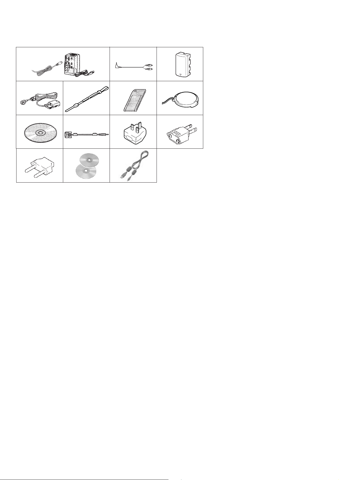
Supplied accessories
123
4567
89!º!¡
!™ !£ !¢
1 AC-VF10 AC power adaptor/charger,
Power cord (1)
2 A/V connecting cable (1)
3 NP-FS11 Battery pack (1)
4 DK-115 DC connecting cable (1)
5 Wrist strap (1)
6 Memory Stick (4MB) (1)
7 Lens cap/Lens cap strap (1)
8 Sony Picture Gear 3.2Lite (1)
(Compact Disk)
9 PC serial cable (1)
!º Conversion plug 3P adaptor (1)
UK, Hong Kong model
!¡ 2-pin conversion adaptor (1)
E model
!™ 2-pin conversion adaptor (1)
Tourist model
!£ USB driver software (1)
!¢ USB cable (1)
SAFETY-RELATED COMPONENT WARNING!!
COMPONENTS IDENTIFIED BY MARK ! OR DO TTED LINE WITH
MARK ! ON THE SCHEMATIC DIAGRAMS AND IN THE PARTS
LIST ARE CRITICAL TO SAFE OPERATION. REPLACE THESE
COMPONENTS WITH SONY PARTS WHOSE PART NUMBERS
APPEAR AS SHOWN IN THIS MANUAL OR IN SUPPLEMENTS
PUBLISHED BY SONY.
SAFETY CHECK-OUT
After correcting the original service problem, perform the following
safety checks before releasing the set to the customer.
1. Check the area of your repair for unsoldered or poorly-soldered
connections. Check the entire board surface for solder splashes
and bridges.
2. Check the interboard wiring to ensure that no wires are
"pinched" or contact high-wattage resistors.
3. Look for unauthorized replacement parts, particularly
transistors, that were installed during a previous repair. Point
them out to the customer and recommend their replacement.
ATTENTION AU COMPOSANT AYANT RAPPORT
À LA SÉCURITÉ!
LES COMPOSANTS IDENTIFÉS P AR UNE MARQUE ! SUR LES
DIAGRAMMES SCHÉMA TIQUES ET LA LISTE DES PIÈCES SONT
CRITIQUES POUR LA SÉCURITÉ DE FONCTIONNEMENT. NE
REMPLACER CES COMPOSANTS QUE PAR DES PIÈSES SONY
DONT LES NUMÉROS SONT DONNÉS DANS CE MANUEL OU
DANS LES SUPPÉMENTS PUBLIÉS PAR SONY.
4. Look for parts which, through functioning, show obvious signs
of deterioration. Point them out to the customer and
recommend their replacement.
5. Check the B+ voltage to see it is at the values specified.
6. Flexible Circuit Board Repairing
• Keep the temperature of the soldering iron around 270˚C
during repairing.
• Do not touch the soldering iron on the same conductor of the
circuit board (within 3 times).
• Be careful not to apply force on the conductor when soldering
or unsoldering.
– 2 –
Page 3

TABLE OF CONTENTS
1. GENERAL ...................................................................1-1
Parts identification.....................................................................1-1
Preparation.................................................................................1-2
1 Charging the battery pack and
“Memory Stick” ...........................................................1-2
2 Installing the battery pack ............................................1-3
3 Setting the date and time ..............................................1-3
Recording .................................................................................. 1-4
Recording still images ..................................................... 1-4
Recording moving images...............................................1-4
Playing back ..............................................................................1-5
Playing back still images .................................................1-5
Playing back moving images........................................... 1-5
Viewing images using a personal computer....................1-5
Various ways of recording .........................................................1-8
Various ways of playback ........................................................1-10
Changing the menu setting ......................................................1-13
Using image data with other equipment ..................................1-14
Additional information ............................................................1-15
2. DISASSEMBLY
• Attachiment of CPC-9 Jig .......................................................2-1
2-1. Removal of Rear Cabinet Block......................................2-2
2-2. Removal of Zoom Lens Block .......................................2-2
2-3 Removal of Cabinet (LT) Block ......................................2-3
2-4. Removal of Lens Block ..................................................2-3
• Service Positionn-1 (Lens Block Area : CD-236, LD-98,
PS-427 and SY-56 Boards)..............................................2-3
2-5. Removal of LCD Panel Block and
Control Switch Block (FK) .............................................2-4
• Service Positionn-2 (Rear Cabinet Area : LCD Panel and
Control Switch Block (FK)) ............................................ 2-4
2-6. Removal of HI-70, DD-131 Boards and
Battery Holder Block.......................................................2-5
2-7. Removal of Upper Cabinet Block and Flash Unit (MC) ...2-5
• Service Positionn-3 (HI-70 and DD-131 Boards) ...................2-6
2-8. Removal of Front Cabinet Assembly............................... 2-6
2-9. Removal and Attaciment of FP-133 Flexible Board .......2-7
2-10. To Fold the New FP-133 Flexible Board ........................2-7
2-11. Removal of Crystal Indication Module ...........................2-8
2-12. Removal of Flash Unit (ST)............................................. 2-8
2-13. Circuit Boards Location ..................................................2-9
2-14. Flexible Boards and Control Switch Block Location...... 2-9
4. PRINTED WIRING BOARDS AND
SCHEMATIC DIAGRAMS
4-1. Frame Schematic Diagram (1) ........................................4-3
Frame Schematic Diagram (2) ........................................ 4-5
4-2. Printed Wiring Boards and Schematic Diagram.............. 4-7
• CD-236 (CCD Imager, Camera)
Printed Wiring Board..............................................4-7
• CD-236 (CCD Imager, Camera)
Schematic Diagram.................................................4-9
• LD-98 (Lens Drive)
Printed Wiring Board............................................ 4-12
• MF UNIT
Schematic Diagram...............................................4-33
• CF/PW (Control Switch Block)
Schematic Diagram...............................................4-33
• HI-70 (LCD Drive, Timing Generator, Video,
Audio, Hi Control)
Printed Wiring Board............................................ 4-35
• HI-70 (LCD Drive)
Schematic Diagram...............................................4-39
• HI-70 (Timing Generator)
Schematic Diagram...............................................4-41
• HI-70 (Video)
Schematic Diagram...............................................4-43
• HI-70 (Audio)
Schematic Diagram...............................................4-45
• HI-70 (Hi Control (1/2) )
Schematic Diagram...............................................4-47
• HI-70 (Hi Control (2/2) )
Schematic Diagram...............................................4-49
• DD-131 (DC/DC Converter)
Printed Wiring Board............................................ 4-51
• DD-131 (DC/DC Converter)
Schematic Diagram...............................................4-53
• FK (Control Switch Block)
Schematic Diagram...............................................4-55
4-3. Waveforms.....................................................................4-57
4-4. Printed Parts Location ...................................................4-59
3. BLOCK DIAGRAMS
3-1. Overall Block Diagram ...................................................3-1
– 3 –
Page 4

5. ADJUSTMENTS
1. Before starting adjustment...............................................5-1
1-1. Adjusting items when replacing main parts and boards..5-2
5-1. Adjustments.....................................................................5-3
1-1. Preparations Before Adjustment......................................5-3
1-1-1.List of Service Tools........................................................5-3
1-1-2.Preparations .....................................................................5-4
1-1-3.Discharging of the strobe power supply ..........................5-4
1-1-4.Precaution ........................................................................5-6
1. Setting the Switch............................................................ 5-6
2. Order of Adjustments ......................................................5-6
3. Subjects ........................................................................... 5-6
4. Preparing the Flash Adjustment Box...............................5-7
1-2. Initialization of B, D, E, F, 7 Page Data .......................... 5-8
1-2-1.Initialization of D Page Data ...........................................5-8
1. Initializing the D Page Data ............................................5-8
2. Modification of D Page Data...........................................5-8
3. D Page Table....................................................................5-8
1-2-2.Initializing the B, E, F, 7 Page Data .............................. 5-11
1. Initializing the B, E, F, 7 Page Data ..............................5-11
2. Modification of B, E, F, 7 Page Data ............................ 5-11
3. F Page table ...................................................................5-11
4. E Page Table .................................................................. 5-14
5. B Page Table..................................................................5-16
6. 7 Page Table ..................................................................5-19
1-3. Video System Adjustments............................................5-21
1. Video Sync Level Adjustment.......................................5-21
(Control Switch Block (FK) )........................................5-21
2. Video Burst Level Adjustment ......................................5-21
(Control Switch Block (FK) )........................................5-21
3. Video Y Level Check..................................................... 5-21
(Control Switch Block (FK) )........................................5-21
1-4. Camera System Adjustments.........................................5-22
1. HALL Adjustment .........................................................5-22
2. Flange Back Adjustment (Using Minipattern Box).......5-23
3. Flange Back Adjustment ...............................................5-24
(Using Flange Back Adjustment Chart) ........................5-24
4. Flange Back Check........................................................5-24
5. Picture Frame Setting ....................................................5-25
6. F No. Standard Data Input.............................................5-25
7. Mechanical Shutter Adjustment ....................................5-26
8. AGC Standard Gain and Max Gain Adjustment ...........5-26
9. Light Level Adjustment and ND SHUTTER CHECK..5-26
10. Auto White Balance Standard Data Input .....................5-27
11. Auto White Balance ND Filter Compensation
Adjustment ....................................................................5-27
12. Auto White Balance Adjustment ...................................5-28
13. Color Reproduction Adjustment....................................5-29
13-1. Color Reproduction Adjustment (Without ND Filter)...5-29
13-2. Color Reproduction Adjustment (With ND Filter)........ 5-29
13-3. Color Reproduction Check ............................................5-30
14. White Balance Check ....................................................5-31
15. Strobe White Balance Adjustment ................................5-31
16. Strobe Light Level and White Balance Check ..............5-32
17. CCD Black Defect Compensation.................................5-32
18. CCD Black Defect Compensation Check ..................... 5-33
19. CCD White Defect Compensation ................................5-34
20. CCD White Defect Compensation Check ..................... 5-34
1-5. LCD SYSTEM ADJUSTMENT ................................... 5-35
1. LCD Initial Data Input .................................................. 5-35
2. VCO Adjustment (Control Switch Block (FK) )...........5-36
3. D Range Adjustment (Control Switch Block (FK) ) .....5-36
4. Bright Adjustment (Control Switch Block (FK) ).........5-37
5. Contrast Adjustment (Control Switch Block (FK) )......5-37
6. Color Adjustment (Control Switch Block (FK) ) ..........5-38
7. V-COM Level Adjustment (Control Switch Block
(FK) ) .............................................................................5-38
8. V -COM Adjustment....................................................... 5-39
9. White Balance Adjustment (HI-70 board).....................5-39
1-6. System Control System Adjustment..............................5-40
1. Battery End Adjustment (SY-54 board) .........................5-40
5-2. Service Mode.................................................................5-41
2-1. Adjustment Remote Commander ..................................5-41
1. Using the adjustment remote commander .....................5-41
2. Precautions upon using the adjustment remote
commander ....................................................................5-41
2-2. Data Process ..................................................................5-42
2-3. Service Mode.................................................................5-43
1. Setting the Test Mode ....................................................5-43
2. Bit value discrimination ................................................5-43
3. Switch check (1) ............................................................5-44
4. Switch check (2) ............................................................5-44
5. LED check .....................................................................5-44
5-3. System Control Adjustment...........................................5-45
1. Initializing the data of pages B, C, D, E, F, 7 ................5-45
2. Inputting the serial No. ..................................................5-45
2-1. Inputting the serial No. ..................................................5-45
6. REPAIR PARTS LIST
6-1. Exploded Views...............................................................6-1
6-1-1.Battery Holder Assembly ................................................6-1
6-1-2.Front Cabinet Assembly .................................................. 6-2
6-1-3.Rear Cabinet Assembly ...................................................6-3
6-1-4.Lens Cabinet Assembly ...................................................6-4
6-1-5.Lens Assembly ................................................................6-5
6-2. Electrical Parts List ......................................................... 6-6
* The color reproduction frame is shown on page 141.
– 4 –
Page 5

SERVICE NOTE
g
[Discharging of the FLASH unit’s charging capacitor]
The charging capacitor of the FLASH unit is charged up to the
maximum 300 V potential.
There is a danger of electric shock by this high voltage when the
capacitor is handled by hand. The electric shock is caused by the
charged voltage which is kept without discharging when the main
power of the DSC-F505 is simply turned off. Therefore, the
remaining voltage must be discharged as described below.
Preparing the Short Jig
To preparing the short jig. a small clip is attached to each end of a
resistor of 1kΩ /1W (1-215-869-11)
Wrap insulating tape fully around the leads of the resistor to prevent
electrical shock.
1kΩ/1W
Wrap insulating tape.
Discharging the Capacitor
Short circuits between the positive and the negative terminals of
charged capacitor with the short jig about 10 seconds.
Capacitor
Short ji
Flash unit (MC)
– 5 –
Page 6
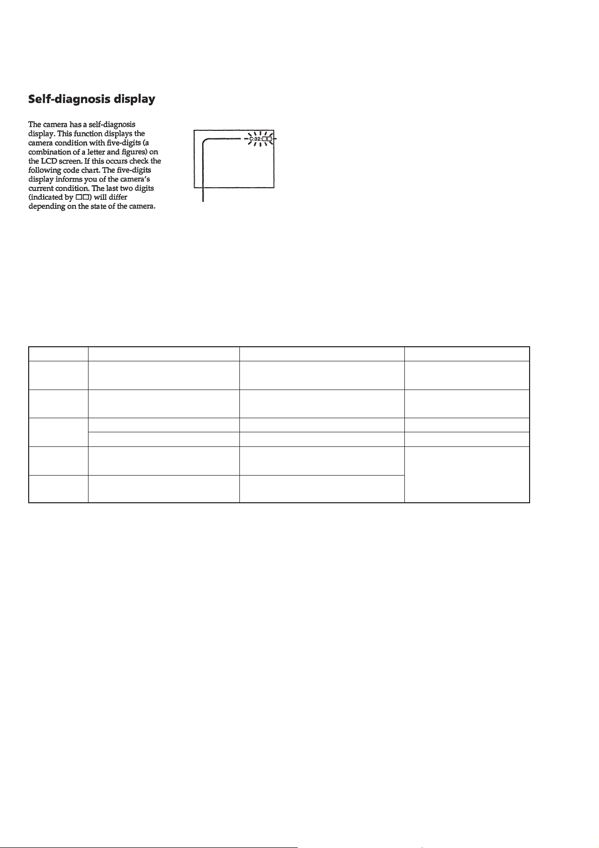
[Description on Self-diagnosis Display]
Self-diagnosis display
• C: ππ: ππ
You can reverse the camera
malfunction yourself. (However,
contact your Sony dealer or local
authorized Sony service facility
when you cannot recover from the
camera malfunction.)
• E: ππ: ππ
Contact your Sony dealer or local
authorized Sony service facility.
Display Code
C:04:ππ
C:32:ππ
C:13:ππ
E:61:ππ
E:91:ππ
Note : The error code is cleared if the battery is removed, except defective
flash, unit.
*1 : The error display is given in two ways.
*2 : When the flash charging failed, Page:D, Address:C7, Data:04 are
written.
After repair, be sure to write Page:D, Address:C7, Data:00.
Use a NP-FS11/F10 battery pack.
Turn the power off and on again.
Format the “Memory stick”.
Insert a new “Memory Stick”.
Checking of lens drive circuit.
*1
Checking of flash unit or replacement
of flash unit.
Countermeasure
You are using a basttery pack that is not an
“InfoLITHIUM” battery pack.
Trouble with hardware.
Unformatted memory stick is inserted.
Memory stick is broken.
When failed in the focus and zoom
initialization.
Abnormality when flash is being
charged.
Cause
Caution Display During Error
for “InfoLITHIUM” BATTERY
ONLY
SYSTEM ERROR
FORMAT ERROR
MEMORY STICK ERROR
—
*2
– 6 –
Page 7
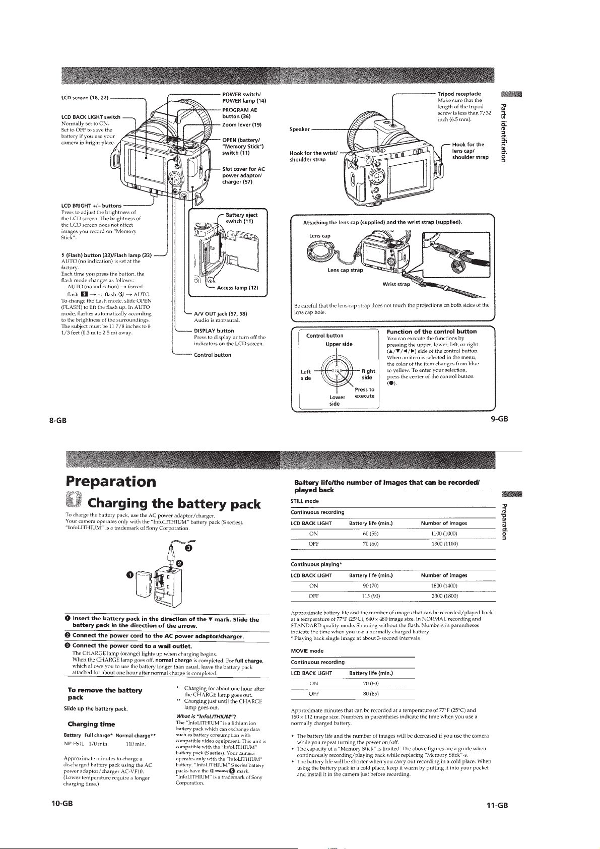
SECTION 1
GENERAL
DSC-F505
This section is extracted from
instruction manual.
1-1
Page 8
1-2
Page 9
1-3
Page 10

1-4
Page 11
1-5
Page 12
1-6
Page 13

1-7
Page 14
1-8
Page 15

1-9
Page 16
1-10
Page 17
1-11
Page 18
1-12
Page 19
1-13
Page 20

1-14
Page 21
1-15E
Page 22
SECTION 2
DISASSEMBLY
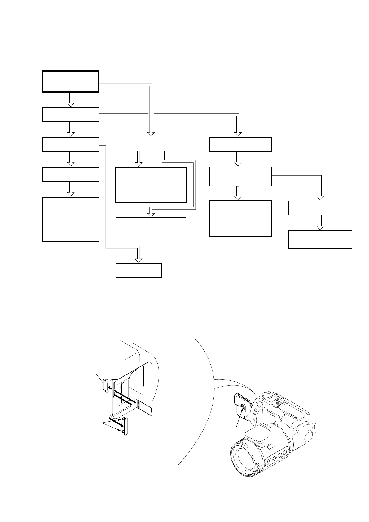
The equipment can be removed using the following procedure.
START
2-1. REAR CABINET BLOCK
2-2. ZOOM LENS BLOCK
DSF-F505
2-3. CABINET (LT) BLOCK
2-4. LENS BLOCK
ATTACHMENT OF CPC-9 JIG
AND
SERVICE POSITION-1
· CD-236 BOARD
· LD-98 BOARD
· PS-427 BOARD
· SY-56 BOARD
2-5. LCD PANEL BLOCK
ATTACHMENT OF CPC-9 JIG
SERVICE POSITION-2
2-11. CRYSTAL INDICATION MODULE
2-12. FLASH UNIT (ST)
• ATTACHMENT OF CPC-9 JIG
CONTROL SWITCH BLOCK (FK)
AND
· LCD PANEL BLOCK
· CONTROL SWITCH BLOCK (FK)
AND OTHER
2-6. HI-70 AND DD-131 BOARDS
BATTERY HOLDER BLOCK
2-7. UPPER CABINET BLOCK
CONTROL SW BLOCK (PW)
FLASH UNIT (MC)
ATTACHMENT OF CPC-9 JIG
AND
SERVICE POSITION-3
· HI-70 BOARD
· DD-131 BOARD
2-8. FRONT CABINET ASSEMBLY
ABOUT FP-133 FLEXIBLE BOARD.
(Refer to 2-9. and 2-10.)
Control switch block (FK)
(CN002)
18
1
CPC-9 jig (J-6082-393-C)
(18p flexible board)
Two claws
CPC cover
Note : Don't use the 12 pin flexible board of CPC-9 jig.
It causes damage to the unit
2-1
Slide the Release knob in the direction of arrow
To open the Battery lid.
A
Release knob
A
.
Page 23

d
NOTE : Follow the disassembly procedure in the numerical order given.
2-1. REMOVAL OF REAR CABINET BLOCK
2
T wo screws
(M1.7)
Front cabinet assembly
4
FP-134 flexible board
(HI-70 board, CN901)
5
Flexible board (Control switch block (FK))
(HI-70 board, CN607)
3
Rear cabinet assembly
6
Harness (HB-50)
(HI-70 board, CN605)
1
T wo screws
(M1.7)
7
Harness (SP-163)
(HI-70 board, CN702)
2-2. REMOVAL OF ZOOM LENS BLOCK
4
5
(SY-56 board)
6
Zoom lens block
CN456
(SY-56 board)
CN455
3
Screw (M1.7)
1
Screw (M1.7)
FP-133 flexible boar
7
2-2
MF ornament
2
Screw (M1.7)
Page 24
b
)
2-3 REMOVAL OF CABINET (LT) BLOCK 2-4. REMOVAL OF LENS BLOCK
)
2
Screw (M1.7)
3
Cabinet (LT) block
5
Harness (SM-114)
(Flash unit (ST), 2P)
Flash unit
(Note)
Cabinet (LT) block
(Bottom view)
(Note)
1
Push the Release kno
4
FP-136 flexible board
(SY-56 board, CN454)
Harness clamp
NOTE : Clamp the cables after attaching the Harness (MS-114). If
clamped with the flash unit closed, the flash unit cannot
be opened, Be sure to clamp the cable with the flash unit
opened.
7
T wo screws
(M1.7)
0
Lens block
6
Cabinet (MF)
assembly
8
Screw (M1.7)
3
CN001
(Control switch block)
5
T wo screws
(M1.7)
2
(SY-56 board)
4
Control switch
block (CF)
9
assembly
CN453
1
Cabinet (LB)
Screw (M1.7
• SERVICE POSITION-1 (LENS BLOCK AREA : CD-236, LD-98, PS-427 and SY-56 BOARDS)
CN602
(HI-70 board)
CN603
(HI-70 board)
FP-133 flexible board
(Not used)
Harness (MS-114)
(to Cabinet (LT) block)
Cabinet (MF) assembly
PS-427 board
Control switch block (CF)
LD-98 board
Rear cabinet block
SY-56 board
Extension cable (33, 39P 0.3 mm)
Parts No. : J-6082-447-A
(HI-70 board, CN602, 603)
(SY-56 board, CN455, 456)
Cabinet (LT) block
(Flash unit (ST))
Harness (MS-114)
(from Front cabinet block)
Lens block
2-3
CD-236 board
Extension cable (39P 0.3 mm
Parts No. : J-6082-448-A
(PS-427 board, CN251)
(CD-236 board, CN101)
Page 25
2-5. REMOVAL OF LCD PANEL BLOCK AND CONTROL SWITCH BLOCK (FK)
8
Control switch block (FK)
Rear cabinet assembly
3
T wo screws
(1.7 x 4)
4
Two screws (1.7)
1
Screw (1.7 x 4)
6
Screw (M1.7)
2
Zoom switch
(RV001)
Button (LCD bright)
Knob (LCD back light)
7
Two screws (M1.7)
5
LCD panel block
(Refer to 2-11. for details diagram on removal of LCD section)
• SERVICE POSITION-2 (REAR CABINET AREA : LCD PANEL and CONTROL SWITCH BLOCK (FK))
Cold cathode fluorescent tube (ND901)
(with Inverter transformer unit)
Control switch block (FK)
CN901
(HI-70 board)
SP901
CN607
(HI-70 board)
Crystal indication module (LCD901)
(with FP-134 flexible board)
Harness (From the SP901)
(HI-70 board, CN702)
2-4
Page 26
2-6. REMOVAL OF HI-70, DD-131 BOARDS AND BATTERY HOLDER BLOCK
1
FP-132 flexible board
(HI-70 board, CN601)
(DD-131 board, CN003)
5
Three screws
(1.7 x 4)
!¡
T wo screws
(1.7 x 4)
8
Screw (M1.7)
0
Battery holder block
9
Screw
(M1.7)
!™
DD-131 board
6
HI-70 board
2
FP-133 flexible board
(HI-70 board, CN602,603)
3
Harness (Microphone)
(HI-70 board, CN701)
7
Harness (MD-97)
(DD-131 board, CN002)
4
Control switch block (PW)
(HI-70 board, CN604)
BB fixed sheet
k
2-7. REMOVAL OF UPPER CABINET BLOCK AND FLASH UNIT (MC)
NOTE : When the flash unit (MC) charging failed, Page : D, Address : C7, Data : 04 are written.
Two claws
After repair, be sure to write Page : D, Address : C7, Data : 00.
3
Upper cabinet block
(Take note of two claws
A
Groove
A
Groove
)
2
Harness (GN-52)
Claw
B
4
Harness (MS-114)
1
Screw (M1.7)
5
Flash unit (MC)
(Take note of claw B)
Details diagram on removal and attachment
of Control switch block (PW)
Claw
(Note)
Edge
Control switch block (PW)
Edge
Flash unit (MC)
Pin
Claw
Hole
Screw (1.7 x 4)
JK retainer assembly
Groove
Claw
Should be fit to the Front
cabinet groove.
Upper cabinet bloc
Claw
Screw (1.7 x 4)
Note for installation of
Flash unit (MC)
2-5
Groove
Page 27

• SERVICE POSITION-3 (HI-70 and DD-131 BOARDS)
)
Control switch block (PW)
Front cabinet block
DD-131 board
FP-133 flexible board
(Not used)
CN456
(SY-56 board)
CN455
(SY-56 board)
CN605
HI-70 board
CN602
CN702
Rear cabinet block
CN603
Harness (HB-50)
Harness (SP-163)
Battery holder block
(To AC power adaptor)
Zoom lens block
2-8. REMOVAL OF FRONT CABINET ASSEMBLY
4
Front cabinet assembly
Extension cable (33, 39P 0.3 mm
Parts No. : J-6082-447-A
(HI-70 board, CN602, 603)
(SY-56 board, CN455, 456)
1
Lift up the Zoom lens block.
3
Screw (M2 x 4)
2
Screw (M2 x 4)
2-6
Page 28
2-9. REMOVAL AND ATTACHIMENT OF FP-133 FLEXIBLE BOARD
NOTE : For folding new FP-133 flexible board, refer to “2-10. To
fold the new FP-133 flexible board” .
FP-133 flexible board
(39P side)
Harness (MS-114)
CN456
(SY-56 board)
CN455
(SY-56 board)
FP-133 flexible board
(33P side)
Harness (GN-52)
FP holder
FP-133 flexible board
(33P side)
When attaching, coil in the direction of
arrow
A
with two and a half revolutions.
(FP-133 flexible board )
A
Hook cover
Harness (GN-52)
FP-133 flexible board
(39P side)
Screw (M1.7)
Screw (M1.7)
Screw (M2 x 4)
Hook the claw of harness
Harness (MS-114)
Hinge cover
Harness (GN-52)
FP guard
2-10. TO FOLD THE NEW FP-133 FLEXIBLE BOARD
: Fold
Adhesive tape
: Fold
1-675-590-xx
FP-133
Adhesive tape
1-675-590-xx
FP-133
Adhesive tape
NOTE : For attaching new FP-133 flexible board, refer to “2-9.
Removal and attachment of FP-133 flexible board” .
Adhesive tape
2-7
Page 29
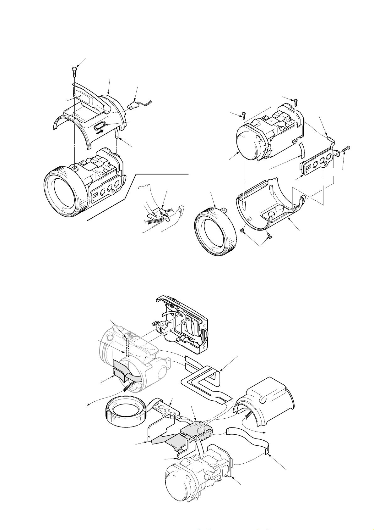
2-11. REMOVAL OF CRYSTAL INDICATION MODULE
Note for installation
Portion
A
3
FP-134 flexible board
Portion
B
Portion C and
5
(Inverter transformer unit)
4
Screw (M1.7)
1
Crystal indication module (LCD901)
(FP-134 flexible board, 24P)
D
Cold cathode fluorescent tube (ND901)
C
B
A
6
Inverter transformer unit
BL cushion
D
BL light interception sheet
2
Screw (M1.7)
2-12. REMOVAL OF FLASH UNIT (ST)
1
Screw
(M1.7 x 4)
BL insulating sheet
5
Flash unit (ST)
Claw
Claw
Claw
4
Cabinet (ST)
(Take note of four claws)
2
FP-136 flexible board
Claw
(Flash unit ST)
2-8
3
Push the Release knob
Page 30

2-13. CIRCUIT BOARDS LOCATION
t
CD-236
(CCD imager, Camera)
LD-98
(Lens drive)
PS-427
(Camera DSP, Memory control)
SY-56
(SH DSP, Memory, Serial I / O, Connector, Digital I / O, )
HI-70
(LCD drive, Timing generator, Video, Audio, HI control)
Flash unit (MC)
Flash unit (ST)
Inverter transformer uni
DD-131
(DC / DC Converter)
2-14. FLEXIBLE BOARDS AND CONTROL SWITCH BLOCK LOCATION
Control switch block (PW)
Control switch block (FK)
FP-132
FP-136
FP-135
Control switch block (CF)
FP-134
FP-133
Lens block
Manual focus block
2-9
E
Page 31

Ver 1.1 1999.10
3-1. OVERALL BLOCK DIAGRAM
DSC-F505
SECTION 3
BLOCK DIAGRAMS
M902
FOCUS
MOTOR
M
FOCUS
RESET
SENSOR
IC402
(SEE PAGE 4-13)
FOCUS
MOTOR
DRIVE
IC406
(SEE PAGE 4-13)
FOCUS, ZOOM
MOTOR
PREDRIVE
M901
ZOOM
MOTOR
ZOOM
MOTOR
DRIVE
TERMINAL
09
M
BT901
BATTERY
S
ZOOM
MOTOR
SENSOR
LENS
HALL
H
IRIS
METER
DRIVE (+)
DRIVE (–)
CAM SO, CAM SI, XCAM SCK
FLASH UNIT (ST) (MC)
FLASH UNIT
DD-131 BOARD
IC001
DC/DC
CONVERTER
(SEE PAGE 4-53)
ST UNREG
BATT SIG
IC403
SHUTTER
DRIVE
(SEE PAGE 4-13)
IC404
IC405
(SEE PAGE 4-13)
IRIS
DRIVE
HALL AMP
SYS DD ON
CAM DD ON
LCD DD ON
CD-236 BOARD
IC101
CCD IMAGER
(SEE PAGE 4-9)
H1, H2
CCD OUT
V1A, V1B, V2A
V3A, V3B, V4
RG, VSHT
LD-98 BOARD
M SHUT ON
ZOOM MOTOR SENS
FOCUS MOTOR SENS
IRIS CONT 1, 2
HALL ADHALL (+)
STRB ON
HALL AD
CAM +15VD
CAM –7.5V
A +4.9V
M +5V
D +2.35V
D +3.2V
A +3.2V
PANEL +13.5V
PANEL +6.5V
PANEL +4.9V
PANEL –15V
BL UNREG
IC407
EVR
(D/A CONV.)
(SEE PAGE 4-14)
CNT C
CNT Y
IC103
A/D CONV.
(SEE PAGE 4-9)
IC102
TIMING
GENERATOR
(SEE PAGE 4-9)
DATA BUS IO
MCK12
MCK14
IC252
SDRAM
64Mbit
(SEE PAGE 4-18)
MIC901
MIC
PS-427 BOARD SY-56 BOARD
IC251
CAMERA DSP
MEMORY CONTROL
VIDEO ENCODER
OPD, OSD, HOST IF
RES CONTROL
SG, JPEG, L-MODE
(SEE PAGE 4-16)
DATA
16
ADDRESS
14
ZOOM MOTOR SENS
FOCUS MOTOR SENS
CNT Y/C
16
16
16
MC XCS1
Y
R-Y/C
B-Y/C
M SHUT ON
DATA BUS
ADDRESS BUS
ADDRESS BUS
9
IC456
SERIAL I/O
SHUTTER CONTROL
FLASH CONTROL
(SEE PAGE 4-29)
STRB ON
CAM SO, CAM SI, XCAM SCK
HOST IF
AUDIO OF
HI-70
BOARD
CY
CNT Y
CNT C
BATT SIG
IC301
VIDEO AMP
(SEE PAGE 4-44)
16
MC XCS3
AU SDTO
AU SDTI
IC455
AUDIO AD/DA CONV.
(SEE PAGE 4-29)
HI SO, HI SI, XHI SCK
REC OUT
IC702
LINE/SPEAKER
AMP
(SEE PAGE 4-45)
EVER +3.5V
IC605
REG
(SEE PAGE 4-49)
HI UNREG
SP+, SP–
(SEE PAGE 4-23)
A OUT L
AUDIO
VIDEO
1623
IC301
MC CAM
SH DSP
MC XCS4
MC XCSO
TXD232C/RXD232C
IC308
EEP ROM
(SEE PAGE 4-25)
R-Y
B-Y
IC601
RESET
(SEE PAGE 4-49)
BACK UP VCC
IC606
RESET
(SEE PAGE 4-49)
SYS DD ON
CAM DD ON
LCD DD ON
M CXCS
(SEE PAGE 4-39)
Y
(SEE PAGE 4-40)
(SEE PAGE 4-41)
HALL AD
BATT SIG
16 16 16
12 12 20 3
MC XCS USB
USB D+
USB D–
IC453
SDRAM
16Mbit
(SEE PAGE 4-28)
IC307
FLASH
ROM
8Mbit
(SEE PAGE 4-25)
IC201
USB IF
(SEE PAGE 4-33)
IC302
IC303
IC304
LOGIC
(SEE PAGE 4-24)
MCX CS
MCX CSO
USB D+/USB –
IC607
EEP ROM
(SEE PAGE 4-50)
IC801
EVR
IC802
LCD DRIVE
BL UNREG
R
G
B
ND901
BACK
LIGHT
UNIT
LCD901
LCD
PANEL
BL ON
IC901
TIMING
GENERATOR
AUDIO
HI SI, HI SO, HI XSCK
XPWR SW
IC603
HI
CONTROL
(SEE PAGE 4-49)
XSHTR LOOK SW
XSHTR SW
MOVIE/STILL SW
XCAM/PW SW
KEY AD1
KEY AD2
KEY AD4
ZOOM SW AD
FOCUS A
FOCUS B
BL ON
IC602
(SEE PAGE 4-50)
TIMER
CLOCK
BL ON
VIDEO
BT601
+
LITHIUM
–
BATTERY
MC XCS MS
MCX CS4
IC306
RS232C DRIVE
(SEE PAGE 4-25)
AUDIO
16
IC451
MEMORY
STICK
IF
(SEE PAGE 4-28)
T1 OUT
R1 IN
XPWR SW
XSHTR LOOK SW
XSHTR SW
MOVIE/STILL SW
XCAM/PW SW
KEY AD1
KEY AD2
ZOOM SW AD
FOCUS A
FOCUS B
KEY AD4
SP901
SPEAKER
MC DIO
MC SCK
CONTROL
SWITCH
BLOCK
(CF)
MF
UNIT
CONTROL
SWITCH
BLOCK
(PW)
R1 OUT
T1 OUT
USB D+
USB D–
POWER
SWITCH
SHUTTER
SWITCH
MOVIE/STILL
PLAY SWITCH
CONTROL
SWITCH
(FK)
FUNCTION
KEY
ZOOM
SWITCH
VIDEO
AUDIO
FUNCTION
SWITCH
MANUAL
FOCUS
CN606
MEMORY
STICK
J001
DIGITAL
I/O
(RS232C)
CN002
DIGITAL
I/O
(USB)
A/V OUT
J001
3-1 3-2E
Page 32

Ver 1.1 1999.10
)
SECTION 4
PRINTED WIRING BOARDS AND SCHEMATIC DIAGRAMS
THIS NOTE IS COMMON FOR WIRING BOARDS AND SCHEMATIC DIAGRAMS
(In addition to this, the necessary note is printed in each block)
DSC-F505
(For printed wiring boards)
• b: Pattern from the side which enables seeing.
(The other layers' patterns are not indicated.)
• Through hole is omitted.
• Circled numbers refer to waveforms.
• There are few cases that the part printed on diagram
isn’t mounted in this model.
• Chip parts.
Transistor Diode
C
5
BE
64
2
13
5
46
2
31
45
2
31
12
4
53
3
21
3
21
3
21
(For schematic diagrams)
• All capacitors are in µF unless otherwise noted. pF : µµF.
50V or less are not indicated except for electrolytics and
tantalums.
• Chip resistors are 1/10W unless otherwise noted.
kΩ=1000Ω, MΩ=1000kΩ.
• Caution when replacing chip parts.
New parts must be attached after removal of chip.
Be careful not to heat the minus side of tantalum capacitor, Because it is damaged by the heat.
• Some chip part will be indicated as follows.
Example C541 L452
22U 10UH
TA A 2520
Kinds of capacitor
Temperature characteristics
External dimensions (mm)
• Constants of resistors, capacitors, ICs and etc with XX indicate
that they are not used.
In such cases, the unused circuits may be indicated.
• Parts with ★ differ according to the model/destination.
Refer to the mount table for each function.
• All variable and adjustable resistors have characteristic curve B,
unless otherwise noted.
• Signal name
XEDIT → EDIT PB/XREC → PB/REC
• 2 : non flammable resistor
• 1 : fusible resistor
• C : panel designation
• A : B+ Line *
• B : B– Line *
• J : IN/OUT direction of (+,–) B LINE. *
• C : adjustment for repair. *
• Circled numbers refer to waveforms. *
*Indicated by the color red.
Note :
The components identified by
mark ! or dotted line with mark
! are critical for safety.
Replace only with part number
specified.
Note :
Les composants identifiés par
une marque ! sont critiques
pour la sécurité.
Ne les remplacer que par une
pièce portant le numéro spécifié.
43
12
(Measuring conditions voltage and waveform)
• Voltages and waveforms are measured between the measurement points and ground when camera shoots color bar chart of
pattern box. They are reference values and reference waveforms.
(VOM of DC 10 MΩ input impedance is used.).
• Voltage values change depending upon input impedance of VOM
used.)
1. Connection
Pattern box
About 90 cm
Front of the lens
2. Adjust the distance so that the output waveform of Fig. a and
the Fig. b can be obtain.
H
Yellow
Cyan
White
Magenta
Green
AABBA=B
Fig. a (Video output terminal output waveform
Cyan
White
Green
Yellow
Magenta
Fig.b (Picture on monitor TV)
When indicating parts by reference number, pleas include
the board name.
Red
Blue
Red
Blue
Electron beam
scanned frame
CRT picture frame
4-1
Page 33

DSC-F505
Ver 1.1 1999.10
4-1. FRAME SCHEMATIC DIAGRAM (1)
1
A
MF UNIT
(CARD EDGE)
B
Q004
BRIGHT
LEVEL
SENSOR
C
LENS
UNIT
CCD
IMAGER
D
E
CD-236
F
BOARD
CONTROL SWITCH BLOCK(CF)
D_3.2V
6
FOUCUS_A
5
FOUCUS_B
4
REGGND
3
PHOTOTR_OUT
2
PHOTOTR_5V
1
CN001 6P
CN004
6P
27PCN401
1
ZOOM_A
2
ZOOM_B
3
ZOOM_A
4
ZOOM_B
Z_SENS_VCC
5
6 Z_SENS_RST
7 Z_SENS_GND
8 HALL(-)
9 BIAS(-)
10 HALL(+)
11 BIAS(+)
12 GND
13 GND
14 DRIVE(-)
15 DRIVE(+)
16 FOCUS_A
17 FOCUS_B
18
FOCUS_A
19
FOCUS_B
20
F_SENS_VCC
TH_OUT
21
22 F_SENS_GND
23 F_SENS_RST
24 ND_CONT(+)
25 ND_DRIVE(+)
26 ND_DRIVE(-)
27 ND_CONT(-)
G
GND
GND
39
CAM_15V
38
CAM_-7.5V
37
A_4.9V
36
A_4.9V
35
A_3.2V
H
I
RESET_CAM/PB
XCS_TG_BEAR
J
K
L
A_3.2V
GND
GND
GND
CAM_DD_ON
PAL/XNT
GND
VSUB_CNT
CAM_SO
XCAM_SCK
CLPOB
EAGLE_STBY
CA_FD
CA_HD
GND
MCK12
MCK24
CA_ADO9
CA_ADO8
CA_ADO7
CA_ADO6
CA_ADO5
CA_ADO4
CA_ADO3
CA_ADO2
CA_ADO1
CA_ADO0
GND
GND
AGC_CONT1
AGC_CONT2
39P CN101
34
33
32
31
30
29
28
27
26
25
24
23
22
21
20
19
18
17
16
15
14
13
12
11
10
9
8
7
6
5
4
3
2
1
39
38
37
36
35
34
33
32
31
30
29
28
27
26
25
24
23
22
21
20
19
18
17
16
15
FLEXIBLE
FP-135
14
13
12
11
10
9
8
7
6
5
4
3
2
1
CAM_15V
CAM_-7.5V
A_4.9V
A_4.9V
A_3.2V
A_3.2V
GND
GND
GND
CAM_DD_ON
PAL/XNT
GND
RESET_CAM/PB
VSUB_CNT
CAM_SO
XCAM_SCK
CLPOB
XCS_TG_BEAR
EAGLE_STBY
CA_FD
CA_HD
GND
MCK12
MCK24
CA_ADO9
CA_ADO8
CA_ADO7
CA_ADO6
CA_ADO5
CA_ADO4
CA_ADO3
CA_ADO2
CA_ADO1
CA_ADO0
GND
GND
AGC_CONT1
AGC_CONT2
39PCN251
5
S001
MACRO
LD-98
BOARD
642
-MOUNT FLEXIBLE-
S002
SPOT
METER
WHT BAL
S003
PE_DAC_LEVEL
AGC_CONT2
LENS_RST_LED
AGC_CONT1
ZM_RST_SENS
FC_RST_SENS
CAM_SCK
CAM_SO
CAM_SI
MC_PB12
MC_PBO9
MC_PBO4
HALL_AD
LENS_TEMP_AD
SP_VOL
MSHUT_ON
30P CN402
A_3.2V
A_3.2V
ND_ON
SYS_V
CNT_Y
CNT_C
MCK12
S004
(W/B SET)
GND
GND
GND
GND
GND
M_5V
M_5V
PS-427
BOARD
1/2 PANEL BLOCK(1/2)
2/2 PANEL BLOCK(2/2)
PANEL_B-Y
Y_OUT
PANEL_R-Y
C_OUT
PANEL_Y
ANS_XIRL4
ANS_XIRL3
ANS_XIRL2
EAGLE_STBY
XCS_TG_BEAR
VSUB_CNT
RESET_CAM/PB
XMACRO_PE
PAL/XNT
MC_A01
MC_A02
MC_A03
MC_A04
MC_A05
MC_A06
MC_A07
CAM_DD_ON
CAM_-7.5V
CAM_15V
MC_XWE1
MC_XWE0
MC_XRD
MC_XCS1
MC_DREQ1
MC_DACK1
XRST_SYS
CAM_SO
XCAM_SCK
FC_RST_SENS
ZM_RST_SENS
LENS_RST_LED
AGC_CONT2
PE_DAC_LEVEL
AGC_CONT1
80P CN252
HDO
CA_FD
MC_A08
MC_A09
MC_A10
MC_A11
MC_A16
MC_A17
MC_A21
MC_A22
MC_A23
MC_D00
MC_D01
MC_D02
MC_D03
MC_D04
MC_D05
MC_D06
MC_D07
MC_D08
MC_D09
MC_D10
MC_D11
MC_D12
MC_D13
MC_D14
MC_D15
D_2.35V
A_3.2V
A_3.2V
A_4.9V
A_4.9V
MCK12
SYS_V
ND_ON
10
GND
D3.2V
D3.2V
80
79
78
77
76
75
74
73
72
71
70
69
68
67
66
65
64
63
62
61
60
59
58
57
56
55
54
53
52
Board TO
51
50
Board
49
48
47
46
45
44
43
42
41
40
39
38
37
36
35
34
33
32
31
30
29
28
27
26
25
24
GND
23
22
21
20
GND
19
18
17
16
15
14
13
12
11
10
9
8
7
6
GND
5
4
3
2
1
80
79
78
77
76
75
74
73
72
71
70
69
68
67
66
65
64
63
62
61
60
59
58
57
56
55
54
53
52
51
50
49
48
47
46
45
44
43
42
41
40
39
38
37
36
35
34
33
32
31
30
29
28
27
26
25
24
23
22
21
20
19
18
17
16
15
14
13
12
11
10
9
8
7
6
5
4
3
2
1
8
CN002 10P
S005
FOCUS
AUTO
MANUAL
30
29
28
27
26
25
24
23
22
21
20
19
18
Board TO
17
Board
16
15
14
13
12
11
10
9
8
7
6
5
4
3
2
1
1 KEY_AD4
2 D_3.2V
3 REG_GND
4 PHOTOTR_5V
5 PHOTOTR_OUT
6 REG_GND
7 REG_GND
8 FOCUS_B
9 FOCUS_A
10 D3.2V
30
A_3.2V
29
A_3.2V
PE_DAC_LEVEL
28
AGC_CONT2
27
26
LENS_RST_LED
25
AGC_CONT1
24
ND_ON
23
ZM_RST_SENS
22
FC_RST_SENS
21
GND
GND
20
19
GND
SYS_V
18
CAM_SCK
17
16
CAM_SO
CAM_SI
15
14
MC_PB12
13
MC_PBO9
MC_PBO4
12
HALL_AD
11
10
LENS_TEMP_AD
9
CNT_Y
8
CNT_C
7
GND
SP_VOL
6
MCK12
5
4
MSHUT_ON
3
GND
2
M_5V
M_5V
1
10PCN453
30PCN452
PANEL_B-Y
Y_OUT
PANEL_R-Y
C_OUT
PANEL_Y
HDO
CA_FD
ANS_XIRL4
ANS_XIRL3
ANS_XIRL2
EAGLE_STBY
XCS_TG_BEAR
VSUB_CNT
RESET_CAM/PB
GND
XMACRO_PE
PAL/XNT
MC_A01
MC_A02
MC_A03
MC_A04
MC_A05
MC_A06
MC_A07
MC_A08
MC_A09
MC_A10
MC_A11
MC_A16
MC_A17
MC_A21
MC_A22
MC_A23
MC_D00
MC_D01
MC_D02
MC_D03
MC_D04
MC_D05
MC_D06
MC_D07
MC_D08
MC_D09
MC_D10
MC_D11
MC_D12
MC_D13
MC_D14
MC_D15
D_2.35V
D3.2V
D3.2V
A_3.2V
A_3.2V
A_4.9V
A_4.9V
CAM_DD_ON
GND
CAM_-7.5V
MCK12
CAM_15V
GND
MC_XWE1
MC_XWE0
MC_XRD
MC_XCS1
MC_DREQ1
MC_DACK1
XRST_SYS
SYS_V
CAM_SO
XCAM_SCK
FC_RST_SENS
ZM_RST_SENS
ND_ON
GND
LENS_RST_LED
AGC_CONT2
PE_DAC_LEVEL
AGC_CONT1
12
13 15
14711 163
2P
FLASH UNIT
(ST)
XSTB_OPEN
1
XSTB_OPEN
2
GND
FP-136
3
GND
FLEXIBLE
4
STB_ON
5
A_4.9V
6
A_4.9V
6P CN454
CN456
39P
SY-56
BOARD
1/6 SH BLOCK(1/2)
2/6 SH BLOCK(2/2)
3/6 MM BLOCK(1/2)
4/6 MM BLOCK(2/2)
5/6 CN BLOCK
6/6 USB BLOCK
80PCN451
LENS_TEMP_AD
33P CN455
REG_GND
REG_GND
CAM_15V
CAM_-7.5V
A_4.9V
A_4.9V
A_3.2V
A_3.2V
D_3.2V
D_3.2V
D.2.35V
D.2.35V
KEY_AD4
PAL/XNT
CAM_DD_ON
HALL_AD
FOCUS_A
FOCUS_B
REG_GND
REG_GND
SP_VOL
CNT_C
CNT_Y
REG_GND
AOUT_L
REG_GND
REC_OUT
REG_GND
PANEL_Y
PANEL_R-Y
PANEL_B-Y
REG_GND
C_OUT
REG_GND
Y_OUT
REG_GND
REG_GND
REG_GND
REG_GND
REG_GND
REG_GND
XSTB_OPEN
MC_HELP
ACCES_LED
MC_XFLRST
XRST_SYS
REG_GND
MC_VCC
MC_BS
MC_DIO
MC_SCLK
MC_INT
MC_MS_IN
SYS_V
XMC_CS
XHI_SCK
REG_GND
MCK12
REG_GND
X232C_DET
R1_OUT
T1_OUT
REG_GND
USB_+
REG_GND
HI_SO
USB_-
1
2
3
4
5
M_5V
6
M_5V
7
8
9
10
11
12
13
14
15
16
17
18
19
20
21
22
23
24
25
26
27
28
29
30
31
32
33
34
35
36
37
38
39
1
2
3
4
5
6
7
8
9
10
11
12
13
14
15
16
17
18
HDO
19
20
21
HI_SI
22
23
24
25
26
27
28
29
30
31
32
33
1
GND
2
GND
3
STB_ON
4
A_4.9V
5
A_4.9V
6
FLEXIBLE
FP-133
6P
179 18
1REG_GND
2DC_300V
MS-114 HARNESS
TO FRAME SCHEMATIC DIAGRAM(2/2)
09
FRAME SCHEMATIC DIAGRAM
4-3 4-4
Page 34

Ver 1.1 1999.10
FRAME SCHEMATIC DIAGRAM (2)
DSC-F505
19
FLASH UNIT(MC)
TO FRAME SCHEMATIC DIAGRAM (1/2)
09
20
4P
MS-114
HARNESS
FLEXIBLE
FP-133
2 REG_GND
1 DC_300V
2P
1ST_GND
2ST UNREG
3STB_CHARGE
4XSTB_FULL
MD-97
HARNESS
39
REG_GND
38
REG_GND
37
CAM_15V
36
CAM_-7.5V
35
M_5V
34
M_5V
A_4.9V
33
32
A_4.9V
31
A_3.2V
30
A_3.2V
29
D_3.2V
28
D_3.2V
27
D.2.35V
D.2.35V
26
25
KEY_AD4
24
PAL/XNT
23
CAM_DD_ON
22
LENS_TEMP_AD
HALL_AD
21
20
FOCUS_A
19
FOCUS_B
18
REG_GND
17
REG_GND
16
SP_VOL
15
CNT_C
14
CNT_Y
13
REG_GND
12
AOUT_L
11
REG_GND
10
REC_OUT
9
REG_GND
PANEL_Y
8
7
PANEL_R-Y
PANEL_B-Y
6
5
REG_GND
4
C_OUT
3
REG_GND
2
Y_OUT
1
REG_GND
33
REG_GND
32
REG_GND
31
REG_GND
30
REG_GND
29
REG_GND
28
XSTB_OPEN
27
MC_HELP
26
ACCES_LED
25
MC_XFLRST
24
XRST_SYS
23
REG_GND
22
MC_VCC
21
MC_BS
20
MC_DIO
19
MC_SCLK
18
MC_INT
17
MC_MS_IN
16
SYS_V
15
HDO
14
XMC_CS
13
XHI_SCK
12
HI_SI
11
HI_SO
10
REG_GND
9
MCK12
8
REG_GND
7
X232C_DET
6
R1_OUT
5
T1_OUT
4
REG_GND
3
USB_+
2
USB_-
1
REG_GND
21
22
23
24
25
27
28
29
3026
31
32
33
34
35
36
A
+
s
-
18P
REG_GND
PANEL_COM
HI_UNREG
LANC_IN
LANC_OUT
BT901
BATTERY
TERMINAL BOARD
SYS_V
HSY
VG
RF7
TXD
RXD
RESET
VDD
1
2
3
4
5
6
7
8
9
10
11
12
13
14
15
16
17
18
CPC
(FOR CHECK)
11
13
15
17
19
21
23
25
27
29
J001
A/V OUT
(MONO)
21P CN604
REG_GND
1
CONTROL SWITCH BLOCK(PW)
REG_GND
2
D+
REG_GND
USB_DET
REG_GND
REG_GND
POWER_LED
SELF_LED
XPWER_SW
REG_GND
XSHTR_LOCK_SW
XSHTR_SW
MOVIE/XSTILL_SW
XCAM/PB_SW
2P
3
-MOUNT FLEXIBLE-
D-
4
5
6
7
R1_IN
8
T1_OUT
9
10
11
12
D_3.2V
13
14
15
16
17
18
19
N.C
20
N.C
21
CN001 21P
CN701
1MIC SIG
2MIC GND
MOVIE
STILL
MIC
S003
POWER
ON/OFF
D007
(POWER LED)
(GREEN)
S002
(SHUTTER)
PLAY
S001
(MODE)
MIC901
D004
(REC LED)
(RED)
CN002
4P
1vcc
2D-
3D+
4GND
J001
DIGITAL
I/O
(SERIAL)
DIGITAL
I/O
(USB)
B
C
D
BACK-LIGHT
CN605
5P
1BL UNREG
2BL GND
HB-50
3BL ON
4BL PWM
HARNESS
5BL LED ON
24 CLD
23 SPD
22 CTR
30PCN901
EX3
1
CTR
3
SPD
5
CLD
7
N.C
9
N.C
N.C
N.C
N.C
N.C
N.C
VGH
VSH
VCC
CLS
EX2
2
VB12
4
RES
6
VR
8
VG
10
VB
12
GND
14
VSH
16
COM
18
VGL
20
VSS
22
MO2
24
MO1
26
EX1
28
SPS
30
21 EX3
20 EX2
19 VB12
18 RES
17
16
15
14
13 GND
12 YSH
COM
11
10
9
FLEXIBLE
FP-134
8 MO2
7 MO1
6
5 SPS
4 CLS
3 VCC
2 VSH
1 VGH
VR
VG
VB
VGL
VSS
EX1
TST (N.C)
24P
UNIT
1 BL UNREG
2 BL GND
3 BL ON
4 BL PWM
5 BL LED ON
5P
LCD901
COLOR
LCD UNIT
ND901
BACK-LIGHT
E
F
G
H
I
J
K
L
M
CN001
GND
GND
2
1
2
1
GND
GND
3P
1BATT UNREG
2BATT SIG
3BATT GND
HI-70
CN002
1 ST_GND
2 ST UNREG
3 STB_CHARGE
4 XSTB_FULL
4P
DD-131
BOARD
CN003 40P
GND
40
40
GND
40P CN601
GND
GND
GND
GND
39
37
38
A_3.2V
GND
GND
GND
36
33
32
35
34
FP-132
33
37
38
39
GND
GND
GND
32
35
34
36
GND
GND
GND
GND
A_3.2V
A_3.2V
31
31
A_3.2V
D_3.2V
30
30
D_3.2V
D_3.2V
29
29
D_3.2V
28
28
D_3.2V
D_3.2V
D_3.2V
27
27
D_3.2V
D_2.35V
26
26
D_2.35V
D_2.35V
CAM+15V
24
FLEXIBLE
25
24
D_2.35V
CAM+15V
CAM-7.5V
23
23
CAM-7.5V
M+5V
22
22
M+5V
PANEL_-15V
M+5V
21
21
M+5V
PANEL_-15V
20
20
GND
CAM_DD_ON
182516
19
18
19
GND
CAM_DD_ON
PANEL+4.9V
LCD_DD_ON
A+4.9V
15
15
A+4.9V
PANEL+6.5V
14
14
PANEL+6.5V
13
12
13
12
PANEL+4.9V
LCD_DD_ON
SYS_DD_ON
PANEL+13.5V
11
10
10
11
SYS_DD_ON
PANEL+13.5V
STB_CHARGE
9
9
STB_CHARGE
GND
A+4.9V
17
17
16
GND
A+4.9V
EVER_3.5V
8
8
EVER_3.5V
HI_UNREG
XSTB_FULL
6
7
7
6
HI_UNREG
XSTB_FULL
55
BAT_SIG
BAT_SIG
BL_UNREG
4
4
BL_UNREG
BL_UNREG
3
3
BL_UNREG
BOARD
1/6 RGB BLOCK
2/6 TG BLOCK
3/6 VI BLOCK
4/6 AU BLOCK
5/6 HI BLOCK(1/2)
6/6 HI BLOCK(2/2)
1Vss
2P
REG_GND
PANEL_COM
KEY_AD3
HI_UNREG
LANC_IN
LANC_OUT
AV_JACK_IN
SYS_V
RESET
CN702
2BS
3NC
10
4DIO
5NC
6INT
7NC
1
8SCLK
9Vcc
10Vss
1SP_OUT-
2SP_OUT+
30PCN607
CN001
2
30P
4
6
HSY
8
10
VG
12
14
16
18
20
RF7
TXD
22
RXD
24
26
VDD
28
30
MEMORY STICK
SP901
SPEAKER
CONTROL SWITCH BLOCK(FK)
-MOUNT FLEXIBLE-
ON
OFF
S006
LCD
BACK LIGHT
ON OFF
S005
LCD
BRIGHT(+)
S007
LCD
BRIGHT(-)
W
T
RV001
(ZOOM)
S002
(FLASH)
D006
(FLASH LAMP)
S003
PROGRAM AE
S001
MENU
(CONTROL BUTTON)
S004
DISPLAY
CN002
BT601
+
LITHIUM
BATTERY
10PCN606
D607
(ACSSES)
39PCN602
1
REG_GND
ZOOM_SW_AD
3
D_3.2V
5
7
STB_LED
REG_GND
9
AU_OUT
11
13
REG_GND
15
REG_GND
REG_GND
17
REG_GND
19
21
V_OUT
REG_GND
23
REG_GND
25
KEY_AD1
27
KEY_AD2
29
33PCN603
4-5 4-6
FRAME SCHEMATIC DIAGRAM
Page 35

DSC-F505
Ver 1.1 1999.10
4-2. PRINTED WIRING BOARDS AND SCHEMATIC DIAGRAM
CD-236 BOARD (SIDE A) CD-236 BOARD (SIDE B)
C
E
D
B
A
C131
R118
14
R120
R119
FB106
C103
1
12
C134
C108
R117
R116
R123
R115
R122
R114
R121
1
39
R124
CL101
09
12345 76891110
2
38
CN101
FB108
C130
48
IC103
15
10
1113
13 24
C129
C109
FB107
R103 R102
Q102
C106
12
L101
C132
C135
C127
37
C126
C125
C121
C119
C110
R112
C139
C105
C137
C136
C107
C128
C118
C115
C123
R113
R109
37
Q101
Q103
C101
R101
C102
FB105
36
R111
C117
FB103
X102
C122
C113
25
987 6
IC102
48
112
C140
IC104
FB109
C104
R104
FB110
R105
FB111
R106
FB104
24
13
FB101
X101
5
10 1
R110
R108
C114
11 20
C112
C111
36
C120
C116
25
C124
C138
L102
C133
IC101
2
L103
3
4
1
1-675-583-
12
CCD IMAGER, CAMERA
CD-236
For printed wiring boards
• This board is six-layer print board. However, the patterns of layers two to five have not been included in
the diagram.
• Chip parts
Transistor
C
BE
There are few cases that the part printed on this
diagram isn’t mounted in this model.
4-7 4-8
Page 36

Ver 1.1 1999.10
DSC-F505
1
CD-236 BOARD
A
CCD IMAGER,CAMERA
-REF.NO.:3000 SERIESXX MARK : NO MOUNT
Note:Resistor are mounted
to the location where
B
FB109,FB110,FB111 are
printed.
C
D
C101
XX
E
F
G
H
I
J
K
09
10
L102
10uH
R113
C138
22u
16V
B
TA
48
P0
S-7.2
47
P0
S-7.2
46
P0
S-7.2
45
P0
S-7.2
44
P0/S-0.3
43
P0
S14.9
42
P0/S-0.3
41
P0/S-7.2
40
P0/S-0.3
39
38
37
100k
C135
10u
20V
TA
C136
0.1u
C137
0.1u
B
VSHT
V3B
F
V3A
V1B
F
V1A
V4
V2
C139
XX
B
1279
FB107
0uH
FB108
0uH
R124
0
1608
C140
XX
B
1
3
VSS2VIN
VOUT
V2153
IC104
XX
1411
TG_DSGAT
TG_RST
VSUB_CNT
B
VSUB_CNT
VSHT
(Note)
FB110
FB111
(Note)
5
R106
C111
10u
6.3V
C112
1u
B
1608
C114
0.1u
B
FB101
0uH
1608
0
0
R108
C113
0.1u
B
FB103
0uH
C117
0.1u
B
(NTSC)
0 (PAL)
FB104
3.1
13
14
15
16
17
18
19
20
21
22
23
24
P0/S2.7
P0/S1.9
H2
4.8
VDD3
3.2
VDD4
P0/S2.5
XSHP
P0/S2.3
XSHD
XRS
P0/S2.7
PBLK
P0.1/S3.1
CLPDM
VSS4
P0/S3.1
CLPOB
P0/S1.8
ADCLK
VSS5
R110
0uH
22
24.375MHz(PAL)
R109
47k
Q103
UN9213J-(K8).SO
PAL/NTSC
SWITCH
1.8
24.54MHz(NT)
0 (NTSC)/3 (PAL)
R104
22
R105
22
XSHP
0
0
V4
V3A
V3B
XSHD
V2
V1A
V1B
84
C123
0.1u
B
P0/S0.9
8RG9
10
11H112
VSS2
VSS3
TIMING GENRATOR
CXD2470R-T4
3.2
3.2
6
7
VDD1
VDD2
IC102
IC102
5
WEN
EBCKSM
C128
0.1u
B
TG_RST
TG_DSGAT
3.1
3.1
1
2
3ID4
RST
VSS1
DSGAT
TEST2
SUB
V3B
V3A
V1B
V1A
678
TEST1
9
1.6
CKO25CKI26OSCO27OSCI28VDD529MCKO30SSI31SCK32SEN33VDI34HDI35VSS6
1.7
3.2
B
0.01u
C122
X101
R111
X102
47
FB105
0uH
36
0
3.1
3.1
3.2
3.1
C132
47u
6.3V
B
TA
VL
VH
V4
V2
VM
26 13 15
FB109
(Note)
0
C106
C104
0.1u
0.1u
1608
B
1608B
C103
0.1u
1005
1
5
P0
R101
S11.4
3300
C102
10p
CH
P0
S10.5
P0/S11.4
P0/S14.8
2SC4178-F13F14-T1
BUFFER
F
Q101
11
12RG13H214H115
VDD
P0/S14.8
VOUT
10
GND
2
P0/S12.6
C105
0.1u
R102
1M
P0/S2.0
GND
7
8NC9
1608B
3
NO MARK : STILL/PB mode
S : STILL mode
P : PB mode
Q102
UN9213J-(K8).SO
SWITCH
0.1
P0/S9.0
C107
R103
0.01u
4700
2012B
P0/S2.0
17
18VL19H120
CSUB
P0/S8.2
4V25
P0/S8.4
P0/S-7.4
V3A3V3B
2
P0/S-7.1
P0/S-0.2
P0/S-0.2
H2
P0/S2.7
V4
1
GND16SUB
P0/S2.7
V1A6V1B
P0/S-0.2
4
1
3
P0/S-7.1
C108
22u
16V
B
TA
IC101
CCD IMAGER
IC101
ICX224AQ-13
P0/S-7.1
C109
10u
20V
TA
100uH
L101
1112
R112
XX
P0/S2.7
18
STBY
0
17
16
3.2
ADCLK
DVDD1
P0/S1.8
15
C129
0.1u
B
14
DVSS3
XSHD
XSHD
P0/S2.3
XSHP
21
XSHP
P0/S3.1
20
P0/S2.5
19
PBLK
CLPOB
IC103
S/H,AGC,A/D CONVERTER
IC103
CCD1000Y-2/2K
3.2
3.2
3.2
3.2
AVDD239AVDD340MODE1
41
42
MODE2
43
AVDD4
44
AVDD5
3.2
1.2
AVSS4
AVSS5
45
46
47
C127
0.1u
B
13
DRVDD
DRVSS
(MSB)D9
14
(LSB)D0
REFN
48
C130
0.1u
B
DRVSS
DVSS1
1.8
REFP
C131
0.1u
B
C134
1u
B
R114
1608
R118
10uH
FB106
0uH
47R119
47
47
R120
47R115
R121
47
47R116
R122
47
47R117
R123
47
47
Precautions Upon Replacing CCD imager
• The CD-236 board mounted as a repair part is not equipped
L103
with a CCD imager.
When replaching this board, remove the CCD imager from the
old one and mount it onto the new one.
• If the CCD imager has been replaced, carry out all the
adjustments for the camera section.
• As the CCD imager may be damaged by static electricity from
its structure, handle it carefully like for the MOS IC.
In addition, ensure that the receiver is not covered with dusts
nor exposed to strong light.
13
3.2
12
0
11
P3.2/S0.5
D8
10
P3.2/s1.1
9
D7
P3.2/S1.5
8
D6
P0/S1.4
7
D5
P0/S1.8
6
D4
P0/S1.3
5
D3
P3.2/S1.3
4
D2
P3.2/S1.7
3
D1
P3.2/S0
2
1
C133
47u
6.3V
B
TA
•
SIGNAL PATH
CHROMA Y/CHROMAY
REC
PB
VIDEO SIGNAL AUDIO
SIGNAL
C110
0.1u
B1608
C115
0.1u
B
1608
C116
0.1u
C118
0.1u
B
P0/S3.1
C124
1u
10
B
2012
C119
0.1u
B
P0/S0.9
P0/S1.2
B
C120
0.1u
B
C121
0.1u
B
P3.1/S1.0
P0.6/S1.6
1.0
22
23
24
FMC
AVSS1
25
CLPDM
CCD_D
26
15
CCD_R
27
AVSS2
28
AGCCNT1
29
AGCCNT2
30
AVSS3
31
1.8
LCM(1.8V)
32
3.2
AVDD1
33
3.2
COMPVIDEO
34
3.2
CGAINCNT
35
0
CHROMA
36
1.4
2.3
CM(1.5V)
2.4V
37
38
C125
0.1u
B
C126
0.1u
B
CL101
39
38
37
36
35
34
33
32
31
30
29
28
27
26
25
24
23
22
21
20
19
18
17
16
15
14
13
12
11
10
9
8
7
6
5
4
3
2
1
GND
CAM_15V
CAM_-7.5V
A_4.9V
A_4.9V
A_3.2V
A_3.2V
GND
GND
GND
CAM_DD_ON
PAL/XNT
GND
RESET_CAM/PB
VSUB_CNT
CAM_SO
XCAM_SCK
CLPOB
XCS_TG_BEAR
EAGLE_STBY
CA_FD
CA_HD
GND
MCK12
MCK24
CA_ADO9
CA_ADO8
CA_ADO7
CA_ADO6
CA_ADO5
CA_ADO4
CA_ADO3
CA_ADO2
CA_ADO1
CA_ADO0
GND
GND
AGC_CONT1
AGC_CONT2
39PCN101
16
TO
PS-427 BOARD
CN251
THROUGH THE
FP135
FLEXIBLE
(SEE PAGE
4-15)
4-9 4-10
CCD IMAGER, CAMERA
CD-236
Page 37

DSC-F505
Ver 1.1 1999.10
LD-98 BOARD (SIDE A)
L401
C411
1426
F
E
L403
30 2
CN402
29 1
D
LD-98 BOARD (SIDE B)
C426
C406
R436
R413
R416
R412
R414
1
4
IC404
C410
8
5
C
R410
C408
C407
B
A
Q401
R415
C409
D401
L404
R406
C424
C423
C412
1
Q405
L402
C420
1
IC406
R432
IC407
11
C425
R438
Q406
C404
2
R437
1
R417
C401
R433
20
1110
R426
C419
R427
D402
R431 R423
CN401
IC402
131
R402
C403
C402
Q403
R434
R435
IC403
C417
C413
C418
C421
110
814
20
R418
C416
R428
R430
R421
IC405
C415 C414
R429
R422
26
27
R425
R424
R419
R420
17
C405
R408
R439
R404
R405
R403
1426
Q402
131
Q404
C422
R409
R411
R407
85
IC401
4
1
09
12345
For printed wiring boards
• This board is six-layer print board. However, the patterns of layers two to five have not been included in
the diagram.
• Chip parts
Transistor
C
BE
64
13
Diode
5
2
3
21
There are few cases that the part printed on this
diagram isn’t mounted in this model.
1-675-586-
12
LENS DRIVE
LD-98
4-11
4-12
Page 38

Ver 1.1 1999.10
DSC-F505
1
LD-98 BOARD
A
LENS DRIVE
-REF.NO.:4000 SERIESXX MARK : NO MOUNT
B
C
D
E
F
G
LENS
UNIT
H
I
J
24
NO MARK : STILL/PB mode
S : STILL mode
P : PB mode
Q406
2SD2216J-QR(K8).SO
ND FILTER DRIVE
4.4
0.70
R438
10
TH_OUT
F_SENS_VCC
FOCUS_B
FOCUS_A
Z_SENS_VCC
ZOOM_B
ZOOM_A
ZOOM_B
ZOOM_A
27P CN401
C404
0.022u
B
27ND_CONT(-)
26ND_DRIVE(-)
25ND_DRIVE(+)
24ND_CONT(+)
23F_SENS_RST
22F_SENS_GND
21
20
19
18
17FOCUS_B
16FOCUS_A
15DRIVE(+)
14DRIVE(-)
13GND
12GND
11BIAS(+)
10HALL(+)
9BIAS(-)
8HALL(-)
7Z_SENS_GND
6Z_SENS_RST
5
4
3
2
1
3 16117 14
C402
1608
B
R403
1u
10k
R402
100k
0.1uBC403
C401
0.01u
IC401
B
4.8
8
NJM2904V(TE2)
IC401
1
0.8
1608
0.8
0.8
0.8
5
6
7
VCC
OUT
IN(-)
IN(+)
OUT
IN(+)
IN(-)
GND
2
3
4
0.8
0.8
S1.1/P4.9
R437
2200
R439
3300
ND FILTER DRIVE
D402
MA111-(K8).S0
5
R404
18k
C405
0.1u
B
1608
2SD2216J-QR(K8).SO
S0.7/P0
R406
10
1608
D401
MA3ZD1200LS0
V2819
25
26
0.3
DGND
UPD16833AGS-9JH
VDD2VM13A1<FA>4PGND15A2<FB>6A3<ZA>7PGND38A4<ZB>9VM410IN111EN112IN213EN2
IC402
1
3.1
4.9
R411
R409
120k
39k
±0.5%
±0.5%
R407
47k
±0.5%
R408
10k
±0.5%
S1.8/P0
Q401
IRIS DRIVE
R410
S1.8/P0
1k
C406
0.022u
B
FOCUS/ZOOM MOTOR DRIVE
21
22
23
24
0
0.3
VM2,3
PGND2
B2<FB>
B1<FA>
B3<ZA>
0.1
0.1
0.1
6
4700
ND FILTER SWITCH
4.8
0
C408
1u
19
20
000
PGND4
B4<ZB>
0.1
R405
±0.5%
Q405
XP4316-(TX).SO
4.9
C409
3300p
B
3.1
8
VCC
NJM2904V(TE2)
IC404
OUT
1
R413
100k
1608
R412
4700
IC402
16
17NC18
3.1
EN4
4.9
S1–2.2/P2.6
8
0.9
0
Q402
UN9213J-(K8).SO
ND ON SWITCH
0
3.1
C410
R415
0.033u
100k
1608
B
0.9
0.9
5
6
7
OUT
IN(-)
IN(+)
0.9
IN(+)
IN(-)
GND
2
3
4
0.9
0.9
C407
R416
0.1u
47k
1608B
R414
10k
14
15
3.1
IN4
EN3
0
C411
0.01u
IN3
C412
33u
10V
TA
0
IC404
IRIS DRIVE
IC405
HALL AMP
2SD2216J-QR(K8).SO
C413
0.1u
B
1608
Q403
0
2SA1832F-Y/GR
(TPL3)
B+ SWITCH
3.1
R417
L401
10uH
B
B
0.5
R418
3.1
R419
1k
1608
±0.5%
AMP
0.1
330
R420
16k
1608
±0.5%
S0.1/P2.0
Q404
4700
R421
R424
100k
C414
0.022u
B
22k
IRIS_CONT1
R422
BA10324AFV-E2
IC405
0.7
0.7
IRIS_CONT2
C415
0.01u
100k
R423
22k
13
14
OUT
OUT
1
2
0.1
CXD2430N-T4
IC406
B
12
IN(-)
S0.4/P1.9
IN(-)
0.1
20
VDD
VDIN2TEST1
1
3.0
R425
IN(+)
IN(+)
3
R426
3.1
S3.2/P0.1
XX
R428
2700
11
GND
S0.3/P3.0
VCC
4
3.1
R427
12k
1200
18
3.0
10
5
0.9
SENS119SENS0
3CS4
R436
2200
R429
180k
R432
180k
R430
180k
C416
0.001u
B
0.9
8
9
OUT
IN(-)
IN(+)
IN(-)
IN(+)
OUT
6
7
0.9
1.2
C418
0.01u
B
C417
3.1
3.1
00
15
17
EN1
DIR1A16DIR1B
SCK5SIN6SOUT7CKOUT
0
3.1
0.2
R431
1608
14
10
S0.5/P1.7
10k
XX
R433
47k
0
EN0
8
1.6
C426
0.1u
CKIN
B
S1–2.2/P1.4
S1–2.2/P2.6
12
DIR0A13DIR0B
XCLR
9
3.1
L403
10uH
±10%
C421
0.01u
C419
1u
1608B
R434
R435
68k
68k
11
TEST0
VSS
10
C422
10u
B
6.3V
TA
L402
10uH
C420
1u
B
1608
12
HALL_REF
HALL_GAIN
HALL_OFFSET
S1.7/P0.6
S1.0/P3.1
0.9
1.5
1.5
1.2
1.2
3.1
1513
IC407
MB88346LPFV-G-BND-ER
GND
1
VSS
AO2
2
AO3
AO1
3
AO4
DI
4
AO5
CLK
5
AO6
LD
6
AO7
DO
7
AO8
AO12
8
AO9
AO11
9
AO10
VCC
10
VDD
C423
0.1u
B
1608
S0.1/P0.6
20
0.3
19
0
18
S3.1/P0
17
16
0
15
1.2
14
13
1.1
12
3.1
11
C424
10u
6.3V
TA
IC407
EVR D/A CONVERTER
L404
10uH
C425
0.1u
B
1608
179 18
30PCN402
1
M_5V
M_5V
2
3
GND
4
MSHUT_ON
5
MCK12
6
SP_VOL
7
GND
8
CNT_C
9
CNT_Y
10
LENS_TEMP_AD
HALL_AD
11
12
MC_PBO4
13
MC_PBO9
14
MC_PB12
15
CAM_SI
16
CAM_SO
CAM_SCK
17
18
SYS_V
19
GND
20
GND
GND
21
22
FC_RST_SENS
23
ZM_RST_SENS
24
ND_ON
25
AGC_CONT1
LENS_RST_LED
26
27
AGC_CONT2
28
PE_DAC_LEVEL
29
A_3.2V
30
A_3.2V
TO
SY-56 BOARD
4-32)
(SEE PAGE
(5/6)
CN452
IC406
FOCUS/ZOOM MOTOR
3.1
3.1
B3<ZA>
4.9
20
4.9
PGND4
19
0
B4<ZB>
0
0
14
15
16
17NC18
IN3
IN4
EN3
EN4
K
IC403
4.9 0
21
22
23
24
25
26
DGND
VM2,3
PGND2
B2<FB>
B1<FA>
SHUTTER DRIVE
L
09
UPD16833AGS-9JH
VDD2VM13A1<FA>4PGND15A2<FB>6A3<ZA>7PGND38A4<ZB>9VM410IN111EN112IN213EN2
IC403
1
3.1
4.9
PRE DRIVE
•
SIGNAL PATH
CHROMA Y/CHROMAY
REC
PB
VIDEO SIGNAL
LENS DRIVE
4-13 4-14
LD-98
Page 39

Ver 1.1 1999.10
DSC-F505
1
CONTROL SWITCH
A
BLOCK(PW)
•
CONTROL SWITCH BLOCK(PW) is
replaced as a block.
So that this PRINTED WIRING
BOARD is omitted.
B
REG_GND
REG_GND
D+
C
D
E
F
TO
SY-56 BOARD
(5/6)
CN604
(SEE PAGE
09
4-48)
D-
REG_GND
USB_DET
REG_GND
R1IN
T1OUT
REG_GND
POWER_LED
SELF_LED
D_3.2V
XPWER_SW
REG_GND
XSHTR_LOCK_SW
XSHTR_SW
MOVIE/XSTILL_SW
XCAM/PB_SW
N.C
N.C
STATIC_GND
LND001
21P
D008
01ZA8.2(TPL3)
CN001
1
2
3
4
5
6
7
8
9
10
11
12
13
14
15
16
17
18
19
20
21
32564
R001
3300
D002
01ZA8.2
(TPL3)
(MODE)
MOVIE
LND003
COM
D003
R003
STILLMOVIE
01ZA8.2(TPL3)
680
LND004
10k
R005
LF001
LF002
VDR001
D004
TLSU1008(T05,SOY)
(REC LED(RED))
PLAYS001
VDR002
R002
2200
FB001
R004
(POWER LED(GREEN))
PLAY
LND002
FB002
1SS387-TPL3
330
CN002 4P
1 VCC
2D-
3D+
4 GND
FB003
D014
(USE for J001 guard)
D007
TLGU1008(T05,SOY)
(SHUTTER)
01ZA8.2(TPL3)
D009
S002
D010
01ZA8.2(TPL3)
J001
1-691-737-21
S003
(1st)
DIGITAL
I/O
SERIAL
S003
POWER
ON/OFF
S107
7
DIGITAL
I/O
(USB)
FB004
(2nd)
1
24
CONTROL SWITCH BLOCK(CF)/MF UNIT
•
CONTROL SWITCH BLOCK(CF)/MF UNIT is replaced as a block.
So that this printed board is omitted.
A
CONTROL SWITCH
BLOCK(CF)
B
C
10
9
8
7
6
5
4
3
2
1
10P
CN002
10k
R006
S001
MACRO
R001
S001
1800
D
E
TO
SY-56 BOARD
(5/6)
CN453
(SEE PAGE
4-31)
09
D_3.2V
FOCUS_A
FOCUS_B
REG_GND
REG_GND
PHOTOTR_OUT
PHOTOTR_5V
REG_GND
D_3.2V
KEY_AD4
6P CN001
SPOT_METER
R002
2700
S002
S002
1PHOTOTR_5V
2PHOTOTR_OUT
3REGGND
4FOCUS_B
5FOCUS_A
6D_3.2V
1 PHOTOTR_5V
2 PHOTOTR_OUT
3 REGGND
4 FOCUS_B
5 FOCUS_A
6 D_3.2V
S003
WHT-BAL
R003
4700
Q004
PN126S-R
7
MF UNIT
C004
2200p
B
1608
(FAR)
RV2
(MANUAL FOCUS)
RV1
(NEAR)
8
653
(BRIGHT LEVEL
S004
SENSOR)
S005
FOCUS
AUTO
MANUAL
R005
S004
39k
S005
LND1
STATIC_GND
6PCN004
(W/B SET)
R004
S003
6800
4-33
4-34
MF UNIT
CONTROL SWITCH BLOCK
/
CF/PW
Page 40

DSC-F505
Ver 1.1 1999.10
HI-70 BOARD (SIDE A)
G
D
C
B
A
E
CN702
CN605
R663
21
C306
R313
F
C315
11
A
C307
R312
Q302
16
IC301
15 17
20
13
R812
C805
12
C804
C308
C803
R817
A
C816
C817
R820
R821
R307
L801
C310
C316
C303
6 8
C807
L802
A
C810
24
C811
A K
D607
Q605
R608
C801
R939
5
R930
R929
09
9
IC902
8
12345 768910
7
5
IC802
4
3
1
2
25 36
12 1
IC801
13 24
R981
R926
R918
C191
R916
R907
R915
C909
R913
R938
C802
R922
R921
4
1
C302
R305
R824
1
R908
D903
R819
R818
R905
48
37
10
R806
R823
1
R909
FB901
C908
L302
32
Q303
R304
R303C311
C312
C309
2
C813
A
1
D304
IC803
32
R649
C808C806
R801
R805
R804
R827R822
R828
2
12
13
C906
24
C907
25 36
L905
R914 C903 R982 R980
11
CN602
C317
CN603
R928
14
IC901
C318
39
1
33
1
Q304
L303
13 12
10
Q701
12
1
C728
C730
R715
C731
Q702
R704
R706
C732
C727
R713
Q706
R607
R635
C605
R650 R641 R646
R636
R642
R651
C632 C618
C631 C617 C619
R733
L704
R732
C723
C612
C610
R627
R626
C729
R672
C613
C614
A
R682
R680
L706
Q704
R721
C740
FB607 FB606
C301
40 2
L301
R314
Q305
C733
R714
C701
R701
C739
R719
FB701
C735
C902
R924
R920
C913
1
48
C905
D902
R912
R908
R910
R976
37
C927
L903
R979
Q705
L901
A
C904
A
C918
R944
C901
R943
D904
39 1
R717
C741
R723 R703
25
C703
C704
R702
R706
C712
36
R707
C711
R729
R709
C713
L902
C917
R942
R705
C714
C716
R711
30 2
29 1
R941
CN601
C734
C744
C724
24
37 48
R725
R726
R720
C715
C721
L701
R968
R967
CN901
C725
IC702
C717
C745
C743
R718
R712
C724
A
C702
R969
C726
13
R681
A
R611
Q603
R612R610
R644
76 50
100 26
Q608
R645
R647
C622
R633
75 51
125
R617
CN607
C624
R654
R656
R634
C623
R6??
D604
C606
R673
230
129
R618
R676
C607
R625
IC603
R657
R609
R606
Q607Q610
R630C633
R658
R659
R622
18
R660 R671 R677
R613
R614
R636
15
C621
C620
X602
R637
R676
R639
BT601
1-675-584-
D602
8
1
R653
R674 R624 C615 C616R626 R643 R670
R661
R662
5
IC602
19
4
C611
12
4-35
LCD DRIVE, TIMING GENERATOR, VIDEO, AUDIO, HI CONTROL
HI-70
For printed wiring boards
• This board is six-layer print board. However, the patterns of layers two to five have not been included in
the diagram.
• Chip parts
Transistor
C
54
BE
2
13
There are few cases that the part printed on this
diagram isn’t mounted in this model.
4-36
Page 41

Ver 1.1 1999.10
HI-70 BOARD (SIDE B)
G
Q612
DSC-F505
Q611
D
C
B
A
E
F
09
R623
IC607
R621
R620
R619
R648
R618
R605
R679
D608
4
1
R667
X601
Q609
1413
LND001
R669
1
R668
CN606
1
10
11 12
C630
12
CN701
C920
R675
R738 R726
23
IC601
R727 R742
1
23
IC606
1
4
L601
A
C608
4
C629
4
5
IC605
3
1
220
FB605
121
CN604
A
C819
C814
C816
C812
C813
A
R932
R934
R935
Q905 Q906 Q903 Q904
A
R933
1-675-584-
LND002
C815
C915
12
C609
Q604
5
8
R604
D606
12345 768910
For printed wiring boards
• This board is six-layer print board. However, the patterns of layers two to five have not been included in
the diagram.
• Chip parts
Transistor
C
5
64
BE
2
13
There are few cases that the part printed on this
diagram isn’t mounted in this model.
4-37
4-38
LCD DRIVE, TIMING GENERATOR, VIDEO, AUDIO, HI CONTROL
HI-70
Page 42

DSC-F505
Ver 1.1 1999.10
1
45
62
7113
9
108
12
HI-70 BOARD(1/6)
A
B
C
D
E
F
G
LCD DRIVE (RGB BLOCK)
-REF.NO.: 2000 SERIESXX MARK : NO MOUNT
NO MARK : STILL/PB mode
1
2
3
4
5
6
7
PANEL_6.5V
A_3.2V
D_3.2V
XHI_SCK
HI_SO
XCS_PANEL_D/A
WIDOV
REG_GND
PANEL_Y
PANEL_R-Y
PANEL_B-Y
TO (5/6)
TO (5/6)
TO (5/6)
TO (5/6)
TO (2/6)
TO (5/6)
TO (5/6)
09
L801
100uH
C801
0.1u
C802
0.1u
R806
47k
COM_ADJ
R804
R805
IC801
C806
0.1u
R801
C808
0.1u
3.2
1.9
2.0
COM-O
0
IC803
TC7SH32FU-TE85R
0
123
3.1
3.2
3.1
4.9
4.9
45
4.9
I/O EXP(EVR)
IC801
B
3.1
3.2
B
H_REV
3.2
V_REV
3.2
NTSC
3.2
COMTST
2.9
0.1
3.0
3.1
13
14
15
16
17
18
0
19
20
21
22
23
24
MB40D001PFV-G-BND-ER
VDD
VCC
H_REV
V_REV
NTSC
COMTST
CLK
SI
SO
XEN
VDDA
VSS
BL_LEVEL
P_MUTE
BRT_TST
V-COM
COM_ADJ
RGB_AMP
CONT
BRT_B
BRT_R
COLOR
BRIGHT
VCO
3.1
12
3.1
11
10
1.8
9
1.2
8
0.9
COM_ADJ
7
2.3
6
2.0
5
1.8
4
2.3
3
COLOR
2
1.1
1
1.9
BRT_B
BRT_R
V-COM
VCO
AMP
C807
47u
6.3V
TA
B
IC803
OR GATE
C803
0.01u
C804
0.01u
0.01u
C805
22k
12k
37
38
39
40
41
42
43
44
45
46
47
48
R818
XX
R819
XX
R827
R828
COM_BLK
XTEST
BRIGHT
CONTRAST
COM_OUT
SUB_CON_B
SUB_CON_R
VCC1
OSD_B
OSD_G
OSD_R
BLACK_IN
15k
33k
R820
XX
R823
12k
R822
39k
1.9
35
36
COM_AMP
COM_BLK_LVL
1
PICTURE1Y/CR/XRGB_SW
2
R821
0
R824
180k
1.1
0.8
33
34
GAMMA2
AGC_FIL3AGC_OUT4AGC_LVL5COLOR6H_FIL_IN7G/Y8R/R-Y/CR9B/B-Y/CB10H_FIL11REG_OUT
3.1
0.8
BRT_B
BRT_R
2.3
2.3
31
32
GAMMA0
SUB_BRT_B
SUB_BRT_R
IC802
LCD DRIVE
IC802
IR3Y37A4
8
0
C817
2.2u
10V
TA
A
C816
0.1u
AMP
29
30
RGB_AMP
1.2
2.4
FRPV
FRP
7
FRPT
2.4
28
COM_FRP
2.0
2.4
27
OUT_LIM
2.0
C815
10u
10V
TA
4.9
25
26
VSH
VCC2
L802
10uH
A
C811
0.1u
6.5
C810
10u
10V
TA
A
P_4.9V
P_3.2V
8
TO (2/6)
9
TO (2/6)
2
2.5
GND1
GND2
24
2.0
23
2.5
22
2.1
21
2.5
20
2.0
19
18
17
16
3.1
15
14
13
4.6
C812
1608
C813
1608
C814
1608
1u
1u
1u
COM-O
FRPV
FRPT
COMTST
NTSC
V_REV
H_REV
V-COM
VCO
COLOR
B_OUT
B_DC_DET
3
4
5
6
2.0
G_OUT
G_DC_DET
R_OUT
R_DC_DET
SYNC_OUT
SYNC_IN
EXT_BGP
SYNC_SEP
12
0
R817
10k
R812
100k
VB
VG
VR
COM-O
FRPV
FRPT
P_XHD
COMTST
NTSC
V_REV
H_REV
V-COM
VCO
REG_GND
10
10
10
11
12
13
14
15
16
6
TO (2/6)
TO (2/6), (5/6)
TO (2/6)
TO (2/6)
TO (2/6)
TO (2/6)
TO (2/6)
TO (2/6)
TO (2/6)
TO (2/6)
H
LCD DRIVE
HI-70 (1/6)
•
SIGNAL PATH
VIDEO SIGNAL
CHROMA Y/CHROMA
Y
REC
PB
4-39 4-40
Page 43

Ver 1.1 1999.10
DSC-F505
1
HI-70 BOARD(2/6)
TIMING GENEREATOR
A
(TG BLOCK)
-REF.NO.: 2000 SERIESXX MARK : NO MOUNT
NO MARK : STILL/PB mode
B
C
D
E
F
G
H
I
J
TO(5/6)
TO(5/6)
TO(1/6)
TO(5/6)
TO(1/6)
TO(5/6)
TO(5/6)
TO(1/6)
TO(1/6)
TO(5/6)
TO(1/6)
TO(1/6)
TO(1/6)
TO(1/6)
TO(1/6)
TO(5/6)
TO(5/6)
17
18
8
19
6
9
10
21
15
11
16
14
12
22
23
13
24
24
L901
P_4.9V
P_3.2V
V-COM
COM-O
V_REV
H_REV
SYS_V
VCO
NTSC
FRPV
FRPT
HDO
P_XHD
10uH
L902
10uH
VB
VG
VR
HSY
PANEL_13.2V
PANEL_-15.3V
PANEL_4.9V
REG_GND
PANEL_COM
COMTST
3 16117 14
L903
10uH
C902
C904
3.3u
0.1u
20V
1608
TA
A
VB
VG
VR
PANEL_COM
V-COM
COM-O
VCO
NTSC
COMTST
V_REV
H_REV
FRPV
FRPT
R979
47k
R978
47k
56
R905
680k
R909
R908
XX
C901
6.3V
TAXXA
C903
0.1u
R906
XX
C905
0.1u
1608
120k
VCO
XXR910
R912
100k
D902
XX
179
LCD901
COLOR
LCD
UNIT
R941
±0.5%
R942
±0.5%
±0.5%
R944
±0.5%
22k
R943
33k
33k
22k
12
D904
MA8047-H-TX
151310
VGVBVR
C918
C917
0.1u
0.01u
C919
C920
1u
1u
35V
3216
A
TA
•
SIGNAL PATH
VIDEO SIGNAL
CHROMA
Y Y/CHROMA
REC
47
47
47
R967
R969
R968
30PCN901
1
EX3
2
EX2
3
CTR
4
VB12
5
SPD
6
RES
7
CLD
8
VR
9
N.C
10
VG
11
N.C
12
VB
13
N.C
14
GND
15
N.C
16
VSH
17
N.C
18
COM
19
N.C
20
VGL
21
N.C
22
VSS
23
VGH
24
MO2
25
VSH
26
MO1
27
VCC
28
EX1
29
CLS
30
SPS
8
IC902
R913
10k
SYNI
SYNC
WIDE
PDPC
NTPC1
TESTI
TEST
VREVC
TESTI
HREVC
COMTST
LOWI
C909
0.1u
2012
C911
560p
R915
1M
C927
2200p
CH
R918
R921
68k
68k
R916
22k
R922
47k
4.9
3.0
4.9
32
33
34
35
36
P15
P16
PDP
MUT
VSEPC
10
IC901
LCD TIMING GENERATOR
13
12
14
BLKI1BLKO2BGPO3HSY4VSY5VIN6GND7SYNO8WIDOV9WIDOT10FRPV11FRPT
2.4
2.4
2.5
4.6
4.7
R920
68k
±0.5%
±0.5%
C913
33k
82p
R924
CH
3.9
2.5
2.4
-10.2
R981
4700
2.5
31
GND
IC901
LZ9GH234
2SD1819A-QRS-TX
30
VDD
R907
XX
D903
C907
0.001u
1T369-01-T8A
L905
6.8uH
2520
R914
1M
C906
C908
0.1u
82p
1608
CH
R980
±0.5%
68k
R982
XX
2.8
37
38
4.9
39
40
3.2
NTSC
V_REV
H_REV
COMTST
41
3.0
42
4.9
43
3.2
44
4.9
45
3.2
46
47
0
48
4.8
IC902
NJM062V(TE2)
1
OUT1
2
IN1-
3
IN1+
4
VCC-
Q903
COM DRIVE
R926
4700
4.9
4.9
29
TST128TST2
0.5
XX
R928
VCC+
OUT2
4.9
27
0
IN2-
IN2+
OSCI
FRPV
COM AMP
13.4
2.3
2.4
25
26
OSCO
TESTO
11
12
2.4
FRPT
R934
0
R933
100k
9
8
1.4
7
0.4
6
0.4
5
13.4
R929
100k
1.4
1.0
R932
R930
100k
33k
24
CLD
23
SPD
22
CTR
21
EX3
20
EX2
19
TESTO
18
RES
17
MODE2
16
MODE1
15
EX1
14
SPS
13
CLS
2.4
13.4
1.7
-10.1
-10.2
R935
2.2
0.5
2.4
0
4.9
2.4
4.9
4.9
0
4.8
3.9
1.3
0
FB901
Q905
2SD1819A-QRS-TX
COM DRIVE
Q904
2SB1218A-QRS-TX
COM DRIVE
Q906
2SB1218A-QRS-TX
COM DRIVE
R939
R938
33k
100k
0uH
V-COM
COM-O
C916
6.8u
16V
A
TA
C915
1u
3216
PANEL_COM
PB
5
TO(1/6)
WIDOV
09
TIMING GENERATOR
4-41 4-42
HI-70 (2/6)
Page 44

DSC-F505
Ver 1.1 1999.10
1
56427113
9
108
HI-70 BOARD(3/6)
A
B
C
VIDEO(VI BLOCK)
-REF.NO.:2000 SERIESXX MARK : NO MOUNT
TO (5/6)
TO (5/6)
TO (5/6)
TO (4/6)
2
33
25
26
A_3.2V
A_4.9V
VOUTON
REF3.2V
NO MARK : STILL/PB mode
S : STILL mode
P : PB mode
L301
47uH
4.8
R312
R313
22k
•
SIGNAL PATH
VIDEO SIGNAL
XX
CHROMA
Y
Y/CHROMA
REC
PB
L302
3.2
2SD2216J-QR(K8).SO
3.8
REG.
10uH
Q302
D
E
F
G
CNT_C
TO (5/6)
TO (5/6)
TO (5/6)
27
CNT_Y
C303
0.1u
B
C_OUT
28
C304
1u
B
Y_OUT
R314
XX
C301
33u
10V
TA
B
29
PAL/XNT
C302
0.1u
B
Q304
XX
SWITCH
C318
XX
CH
C317
L303
XX
1608
XX
CH
R305
XX
C306
47u
6.3V
TA
C307
0.1u
B
B
17
C308
1u
C310
B
1608
0.1u
B
2
1.8 1.3 3.2 4.8
14
15
16
17
18
19
20
V+1
C313
TA
CIN2/INSEL
R303
10V
A
V+2
1M
R304
1k
1.3
COUT
0
UN9213J-(K8).SO
CIN1
CLAMPREF
NJM2538BV(TE2)
15
IC301
1
1.5 1.3 1.3 1.3
C309
0.1u
B
GAINCTL/PWSAVE
YIN12GAINCTL/MUTE3YIN24CLAMP5CHARA6BLANK7WIDE8GND9YOUT10YSAG
B
C311
0.1u
B
XX
C312
10u
13
SDCOUT
16
Q303
S2.0/P1.6
12
VOUT
11
VSAG
S1.8/P1.5
C315
22u
A
4V
TA
C316
100u
4V
C
TA
IC301
VIDEO AMP
R307
68
V_OUT
REG_GND
<VIDEO_GND>
30
31
TO (5/6)
TO (5/6)
SWITCH
Q305
09
XX
SWITCH
VIDEO
HI-70 (3/6)
4-43 4-44
Page 45

Ver 1.1 1999.10
DSC-F505
1
HI-70 BOARD(4/6)
A
AUDIO (AU BLOCK)
-REF.NO.: 2000 SERIESXX MARK : NO MOUNT
NO MARK : STILL/PB mode
S : STILL mode
P : PB mode
B
C
32
TO(5/6)
<AU_GND>
D
TO(5/6)
E
TO(5/6)
F
TO(5/6)
G
H
I
J
K
09
MIC901
MIC
C701
0.022u
R701
±0.5%
4
C702
10V
10u
C703
R702
3300
±0.5%
0
1608
C704
0.01u
B
1608
B
1608
3300
C738
XX
2
REG_GND
35
AOUT_L
33
A_4.9V
34
REC_OUT
3 117 14
L701
10uH
2P
CN701
1MIC SIG
2MIC GND
R726
1200
C742
R727
XX
0
56
C725
0.47u
IC702
LINE AMP,
SPEAKER AMP
R723
0
C711
4.7u
C712
1u
6.3V
P
TA
0.015u
1608
C714
6.3V
R707
27k
±0.5%
1.6
1.6
XXR703
1.6
1.6
TA P
1.6
47k
R708
S1.6/P0
R709
56k
±0.5%
C713
0.015u
B
1608
C716
XX
B
1005
B
C715
0.01u
B
8
B
1608
C744
3.2
C741
10u
6.3V
TA P
3.2
1.6
25
REC_OUT
26
HPF_BIAS
27
LPF_IN
28
HPF_OUT
29
HPF_IN
30
AGC_OUT
31
GND
0
32
AGC_DET
33
WHPF_OUT
S1.6/P0
34
WHPF_BIAS
1.6
35
WHPF_IN
36
LING_IN
2.4
R711
15k
R729
XX
±0.5%
XX
1.6 3.2
R724
20NC21
22
23
24
VCC
VREF
STBY
MIC_OFF
AN2904FHQ-EB
2.4
2.4
3.1
MIC_OUT39WIND_ON40MIC_IN412VOUT42VREG_C43VREF_H44VCCH45GND46LINE_OUT47SP_SAVE48SP_VCC
GAIN_SET
37
38
0R728
B
2.4
0.1u
C721
R705
2200
R720
1k
R725
C717
10u
6.3V
0.01u
B
2.4
15NC16
VOL_CTL
4.9
C745
0.1u
1608
14
13
BUF_IN
BUF_OUT
VOL_OUT
SLPF_IN
SLPF_OUT
MIX_IN
BEEP_IN
AGND
MIX_OUT
SPA_IN
VREF_SP
SP_OUT-
SP_GND
SP_OUT+
4.3
3.1
2.4
B
1.3
1.6
17
18NC19
AGND
PB_IN
IC702
2.4
2.4
100
1u
C743
B
1608
C724
10u
6.3V
TA P
C730
10u
6.3V
B0.47uC726
2.2
2.2
2.2
2.2
R712
2200
R704
12
11
XX
R732
10
R733
2.2
9
1608
2.2
8
2.2
7
R715
2.2
6
2200
C729
5
10u
6.3V
2.2
4
2.2
TA P
3
2
1
2.2
C727
10u
10V
C728
10u
6.3V
TA P
C723
XX
B
0
0
0
Q701
UN9216J-(K8).SO
MUTE
9
R717
B
C733
0.47u
R714
68k
L704
10uH
R706
XX
C731
0.01u
B
C732
0.01u
B
S3.2/P0
R713
100k
S-0.2/P3.2
UN9113J-(K8).SO
3.2
22k
Q702
MUTE
FB701
3.8
3.2
0uH
R718
2200
5.0
4.3
R719
47k
C734
3.1
4.9
2SA1586YG-TE85L
REF 3.2V REG
C735
10u
6.3V
TA P
1u
B
5.0
R721
470
Q705
UN9215J-(K8).SO
B+ SWITCH
4.3
Q704
FMMT617TA
B+ SWITCH
Q706
C739
0.01u
B
•
SIGNAL PATH
REC
12
PB
C740
1u
B
AUDIO SIGNAL
151310
BEEP
36
AU_SPON
XAU_MUTE
SP_VOL
CN702
1 SP_OUT-
2 SP_OUT+
L706
10uH
M_5V
A_3.2V
REF3.2V
AU_OUT
REG_GND<AU_GND>
TO(5/6)
37
TO(5/6)
2P
SP901
SPEAKER
38
TO(5/6)
2
TO(5/6)
26
TO(3/6)
39
TO(5/6)
32
TO(5/6)
4-45 4-46
AUDIO
HI-70 (4/6)
Page 46

DSC-F505
Ver 1.1 1999.10
HI CONTROL (1/2)
HI-70 (5/6)
1
HI-70 BOARD(5/6)
A
CONNECTOR (HI BLOCK(1/2))
-REF.NO.: 2000 SERIESXX MARK : NO MOUNT
NO MARK : STILL/PB mode
B
C
D
E
F
G
H
I
J
K
L
M
N
•
SIGNAL PATH
O
P
CHROMA Y/CHROMAY
REC
PB
09
(SEE PAGE
MEMORY STICK
TO
SY-56 BOARD
(5/6)
CN455,456
THROUGH THE
FP-133
FLEXIBLE
(SEE PAGE
VIDEO SIGNAL AUDIO
SIGNAL
TO
CONTROL SWITCH
BLOCK(FK)
CN001
4-55)
4-31)
74
30P CN607
1
REG_GND
2
REG_GND
3
ZOOM_SW_AD
4
SYS_V
5
D_3.2V
6
HSY
7
STB_LED
8
PANEL_COM
9
REG_GND
10
KEY_AD3
REG_GND
HI_UNREG
REG_GND
LANC_IN
REG_GND
LANC_OUT
REG_GND
REG_GND
REG_GND
KEY_AD1
KEY_AD2
AV_JACK_IN
LAND002
MECA_GND
110
LND001
MECA_GND
33P CN603
REG_GND
REG_GND
T1_OUT
R1_OUT
X232C_DET
REG_GND
REG_GND
XHI_SCK
XMC_CS
MC_MS_IN
MC_INT
MC_SCLK
MC_DIO
MC_VCC
REG_GND
XRST_SYS
MC_XFLRST
ACCES_LED
MC_HELP
XSTB_OPEN
REG_GND
REG_GND
REG_GND
REG_GND
REG_GND
REG_GND
REG_GND
CAM_15V
CAM_-7.5V
D.2.35V
D.2.35V
KEY_AD4
PAL/XNT
CAM_DD_ON
LENS_TEMP_AD
HALL_AD
FOCUS_A
FOCUS_B
REG_GND
REG_GND
SP_VOL
REG_GND
AOUT_L
REG_GND
REC_OUT
REG_GND
PANEL_Y
PANEL_R-Y
PANEL_B-Y
REG_GND
REG_GND
REG_GND
39P_CN602
AU_OUT
V_OUT
RESET
Vss
Vcc
SCLK
NC
INT
NC
NC
BS
Vss
USB_-
USB_+
MCK12
HI_SO
HI_SI
SYS_V
MC_BS
A_4.9V
A_4.9V
A_3.2V
A_3.2V
D_3.2V
D_3.2V
CNT_C
CNT_Y
C_OUT
Y_OUT
FB606
11
0uH
12
VG
13
14
15
16
17
18
19
20
RF7
FB607
21
0uH
22
TXD
23
24
RXD
25
26
27
28
VDD
29
30
CN60610P
10
9
8
7
6
5
4DIO
3
2
1
1
2
3
4
5
6
7
8
9
10
11
12
13
14
15
HDO
16
17
18
19
20
21
22
23
24
25
26
27
28
29
30
31
32
33
39
38
37
36
M_5V
35
M_5V
34
33
32
31
30
29
28
27
26
25
24
23
22
21
20
19
18
17
16
15
14
13
12
11
10
9
8
7
6
5
4
3
2
1
ZOOM_SW_AD
SYS_V
D.32V
STB_LED
KEY_AD3
KEY_AD1
KEY_AD2
AV_JACK_IN
MC_SCLK
MC_INT
MC_DIO
MC_BS
HI_SO
HI_SI
XHI_SCK
XMC_CS
SYS_V
MC_MS_IN
MC_INT
MC_SCLK
MC_DIO
MC_BS
XRST_SYS
XFL_RST
MC_HELP
R649
47k
KEY_AD0
KEY_AD4
CAM_DD_ON
LENS_TEMP_AD
HALL_AD
FOCUS_A
FOCUS_B
HSY
PANEL_COM
AU_OUT
VG
LANC_IN
LANC_OUT
RF7
V_OUT
TXD
RXD
RESET
VDD
REG_GND
X232C_DET
REG_GND
HDO
REG_GND
PAL_XNT
SP_VOL
CNT_C
CNT_Y
AOUT_L
REC_OUT
PANEL_Y
PANEL_R-Y
PANEL_B-Y
C_OUT
Y_OUT
8103 16
9
1125
Note :
The components identified by
24
TO (2/6)
21
TO (2/6)
39
TO (4/6)
10
TO (2/6)
42
TO (6/6)
43
TO (6/6)
44
TO (6/6)
30
TO (3/6)
45
TO (6/6)
46
TO (6/6)
21P CN604
REG_GND
REG_GND
REG_GND
USB_DET
REG_GND
T1_OUT
REG_GND
POWER_LED
SELF_LED
XPWR_SW
REG_GND
XSHTR_LOCK_SW
XSHTR_SW
MOVIE/XSTILL_SW
XCAM/PB_SW
R608
680
D607
CL-220UR-C-TS
ACSSES
1.9
Q605
UN9213J-(K8).SO
LED DRIVE
CN605
40P CN601
BL_UNREG
BL_UNREG
BAT_SIG
HI_UNREG
XSTB_FULL
EVER_3.5V
STB_CHARGE
PANEL+13.5V
SYS_DD_ON
PANEL+4.9V
LCD_DD_ON
PANEL+6.5V
A+4.9V
A+4.9V
CAM_DD_ON
PANEL_-15V
CAM-7.5V
D_2.35V
CAM+15V
D_2.35V
D_3.2V
D_3.2V
D_3.2V
D_3.2V
A_3.2V
A_3.2V
22
32
29
37
27
35
34
31
47
6
TO (4/6)
TO (4/6)
7
28
TO (3/6)
TO (6/6)
TO (6/6)
TO (2/6)
TO (4/6)
TO (3/6)(6/6)
TO (4/6)
TO (3/6)
TO (1/6)
TO (3/6)
CAM_15V
CAM_-7.5V
D_2.35V
A_3.2V
D_3.2V
ND901
(BACK-LIGHT)
M_5V
TO
CONTROL SWITCH
BLOCK(PW)
BACK
LIGHT
UNIT
(FOR LCD)
(SEE PAGE
4-34)
HB-50
HERNESS
TO
DD-131 BOARD
CN003
THROUGH THE
FP-132
FLEXIBLE
(SEE PAGE
4-54)
0
mark ! or dotted line with mark
! are critical for safety.
Replace only with part number
specified.
1
2
3
D+
4
D-
5
FB605
6
0uH
7
8
R1_IN
9
10
11
12
13
D_3.2V
14
15
16
17
18
19
20
N.C
21
N.C
5P
1BL UNREG
2BL GND
3BL ON
4BL PWM
5BL LED ON
1
GND
2
GND
3
4
5
6
7
8
9
10
11
12
13
14
15
16
GND
17
GND
18
19
M+5V
20
21
M+5V
22
23
24
25
26
27
28
29
30
31
32
GND
33
GND
34
GND
35
GND
36
GND
37
GND
38
GND
39
GND
40
A_3.2V
D_3.2V
HI_UNREG
EVER_3.5V
PANEL_13.2V
PANEL_4.9V
PANEL_6.5V
A_4.9V
M_5V
REG_GND
PANEL_-15.3V
D_3.2V
4-47 4-48
A_3.2V
USB_D+
USB_D-
T1_OUT
R1_IN
XP4113-TXE
SWITCH
33
38
Q611
40
41
TO (6/6)
17
19
TO (3/6), (4/6)
18
TO (4/6)
2
2
6
0
0
TO (6/6)
TO (2/6)
TO (2/6)
1
TO (1/6)
TO (2/6)
TO (1/6), (6/6)
TO (1/6), (4/6)
TO (1/6)
14612
1513
17
Note :
Les composants identifiés par une
marque ! sont critiques pour la
sécurité.
Ne les remplacer que par une
piéce portant le numéro spécifié.
USB_DET
PWR_LED
XSELF_LED
XPWR_SW
XSHTR_LOCK_SW
VOUTON
SYS_V
AU_SPON
XSHTR_SW
BL_LED_ON
BL_ON
XBL_PWM
CAM_DD_ON
VOUTON
XCS_PANEL_D/A
SYS_V
AU_SPON
BEEP
BEEP
XAU_MUTE
TO_HI-70_BOARD(6/6) A
MOVIE/XSTILL_SW
XCAM/PB_SW
4.9
5.0
R606
120
CAM_-7.5V
0
D_2.35V
CAM_15V
0
0
XP4213-TXE
SWITCH
TO (1/6)
Q612
3
TO (1/6)
TO (4/6)
0
HI_SO
XHI_SCK
TO (3/6)
TO (2/6)
4
SYS_DD_ON
LCD_DD_ON
36
HI_SO
XHI_SCK
BAT_SIG
XSTB_FUL
STB_CHG
25
XCS_PANEL_D/A
23
XAU_MUTE
Page 47

Ver 1.1 1999.10
DSC-F505
19
HI-70 BOARD(6/6)
HICONTROL (HI-BLOCK(2/2))
-REF.NO.: 2000 SERIESXX MARK : NO MOUNT
NO MARK : STILL/PB mode
S : STILL mode
P : PB mode
40
TO (5/6)
TO (5/6)
TO (5/6)
09
HI_UNREG
41
EVER_3.5V
REG_GND
6
TO HI-70 BOARD(5/6)
TO (5/6)
47
X232C_DET
20
22 24
23 322518
26 3633
27 3521
29
30
31 34
37
A
R675
0
C630
IC605
+3.1V REG
IC605
RN5RZ31BA-TL
3.9
45
EN
NC
GND
VIN
VOUT
123
3.9
3.1
C629
33u
10V
TA
B
A
XX
L601
10uH
±10%
C608
22u
6.3V
TA A
B
TO (5/6)
TO (5/6)
TO (5/6)
IC606
S-80820ANNP-EDH-T2
3
N.C.
4
XRESET
Vss
IC606
RESET
IC601
S-80827HNNP-A9A-T2
3
N.C.
4
XRESET
Vss
IC601
RESET
LANC_IN
42
LANC_OUT
43
PAL/XNT
29
XCS_EEPROM
VOUTON
0
R680
STB_CHG
HALL_AD
2200
R682
LENS_TEMP_AD
ZOOM_SW_AD
1k
470k
R672
R628
KEY_AD4
KEY_AD3
KEY_AD2
KEY_AD1
KEY_AD0
1M
10k
10k
10k
10k
R650
R641
R644
R635
R627
470k
R646
1k
1k
1k
R6451kR642
R6361kR651
R647
B
B
B
B
B
XX
XX
XX
XX
XX
C617
C618
C632
C631
C619
D_3.2V
2
TO (5/6)
IC607
XFL_RST
2
Vdd
3.1
1
3.1
2
Vdd
3.1
1
3.1
C610
0.1u
B
B
B
0.1u
0.01u
C612
C613
AU_SPON
B
XX
C614
EEPROM
AK6440BH-E2IC607
3.2
VCC
8
N.C
7
C609
RST
6
3.1
GND
5
RTS_SCK
RTS_SIO
XRST_SYS
XAU_MUTE
BL_LED_ON
XEEPROM_WE
XPWR_SW
XCAM/PB_SW
XSHTR_SW
XSHTR_LOCK_SW
MC_MS_IN
MOVIE/XSTILL_SW
XMC_CS
XCS_EEPROM
RTS_CS
CAM_DD_ON
BEEP
470k
R604
0
3.1
S3.1/P0
USB_DET
3.5
S0.1/P1.8
FOCUS_B
FOCUS_A
MC_HELP
XSELF_LED
PWR_LED
XBL_PWM
STB_LED
XCS_EEPROM
XHI_SCK
HI_SO
HI_SI
XEEPROM_WE
SYS_V
1
CS
3.0
2
SCK
2.9
3
DI
0.1
4
DO
2.7
19
0.2
1.5
1
XIN
IC602
CLK_OUT
IC602
TIMER CLOCK
SIO
VDD
S-3513BEFS-TB
8
3.0
RTS_SIO
RTS_SCK
RTS_CS
D608
BT601
LITHIUM
BATERY
BAT_SIG
XXR638
XXR637
470kR614
470kR609
R676
R677
XX
R607
R610
0
4700
C605
0.001u
B
470kR615
470kR639
D604
1SS388(TPL3)
XX
100k
100k
R613
R616
470kR618
100kR619
100kR620
100kR621
XX
Q603
3.2
0
MODULATOR
0
R611
10k
R622
R681
2700
0
R612
XX
C606
C607
XX
3.3u
B
16V
TA
R617
100k
R673
R657
R658
R659
R660
R671
R623
XX
0
Q604
UN9213J-(K8).SO
MODULATOR
47kR678
0
LANC_IN
1
0.3
2
LANC_OUT
3
C627
XX
B
R674
PAL
4
SIRCS_IN
5
N.C
6
N.C
3.1
7
RTS_SCK
3.0
8
RTS_SIO
1k
3.2
9
XRST_SYS
S3.2/P0
10
XAU_MUTE
0
11
BL_LED_ON
3.1
XEEPROM_WE
12
GND
13
1k
3.0
XPWR_SW
14
1k
S0/P2.9
XCAM/PB_SW
15
1k
3.0
16
XSHTR_SW
1k
3.0
XSHTR_LOCK_SW
17
3.2
18
MS_IN/DISK_IN
19
VERTICAL
3.0
20
XHAND_SENS
1k
0
21
XSTILL/MOVIE_SW
2.6
XMC_CS
22
3.1
XCS_EEPROM
23
0.1
RTS_CS
24
S3.1/P0
25
CAM_DD_ON
470k
R679
XX
0
44
TO (5/6)
RF7
TXD
RXD
TO (5/6)
45
RESET
VDD
46
TO (5/6)
3.1
3.103.103.200
96
97
98
99
100
SP_ON
XRST_FLASH
(EVF_DD_ON)
WIND_FIL_SEL
XRST_MELODY
95
(XCS_EEPROM)
94
VOUTON
93
STB_CHG
91
92
HALL_AD
DD_OUT_DET
HI CONTROL
1.5
89
90
ZOOM_SW
LENS_TMP_AD
IC603
IC603
S579615PZ-TEB
88
GND
3.1
3.1
87
BACKUP_VCC
3.2
85
86
BACKUP_VCC
3.2
3.2
3.2
3.2
3.2
3.2
3.2
3.1
77
81
83
KEY_AD482KEY_AD5
(KEY_AD6)84(KEY_AD7)
KEY_AD078KEY_AD179KEY_AD280KEY_AD3
BACKUP_VCC
18
XCS_PANEL_D/A26XCS_MELODY27(XCS_EVF_D/A)28SYS_DD_ON29AV_JACK_IN30X232C_DET31XSTB_FUL32NC33NC34NC35MELODY36(TEST MODE)37XRESET38GND3920MHZ_OUT4020MHZ_IN41BACKUP-VCC42BL_ON43HI_SI44HI_SO45XHI_SCK46LCD_DD_ON47BATT_SI48BATT_SO49(XMC_CS)
3.1
3.1
XCS_PANEL_D/A
SYS_DD_ON
3.0
AV_JACK_IN
003.1
1.6
1.803.1
2.7
2.9
0.1
0.3
0.3
0
3.0
47k
R624
XSTB_FUL
R626
1k
C616
C615
0.1u
0.022u
B
3.1
10
R643
B
XMC_CS
HI_SI
LCD_DD_ON
BL_ON
HI_SO
XHI_SCK
3.1
76
BACKUP_VCC
XLI_PRE_END
MELODY_ENV
2.8
50
0
R670
BACKUP_VCC
(FOCUS_B)
XDRY_BATT
BATT_SENS
(FOCUS_A)
USB_DET
MC_HELP
CHARGE_INH
BATT_IN
POWER_LED
SELF_LED
XBL_PWM
S3.1/PO
STB_LED
(REC_LED)
32KHZ_OUT
32KHZ_IN
BACKUP_VCC
R625
100k
330k
HN1L02FU(TE85R)
0.3
3.3
R654
C624
C633
0.1u
B
Q609
IF BLOCK
3.1
0.3
R669
100k
3.1
75
GND
74
0
73
1.5
72
2.9
71
0
70
3.1
3.1
2.8
SYS_V
3.1
GND
1.3
3.1
R648
1M
R668
69
470k
68
67
NC
66
R630
65
1M
64
NC
63
NC
62
61
60
0
59
0
58
0
57
56
55
54
53
52
51
X601
20MHz
C622
0.1u
B
R656
1M
R633
100k
R634
Q610
UN9213J-(K8).SO
LED DRIVER
Q608
UN9213J-(K8).SO
LED DRIVER
Q607
UN9213J-(K8).SO
LED DRIVER
C620
0.1u
B
R662
R661
D602
1SS388(TPL3)
100k
C623
0.1u
B
0.1
100k
R653
32.768kHz
X602
C611
22p
CH
2
3
4
VSS
XOUT
0.5
XSCK
5CS6
7
0.1
3.0
3.0
10k
10k
R663
270
MAZS082008SO
0.1u
B
C621
XX
1608
R667
100k
2.7
D606
1SS387-TPL3
B
C
D
B
E
100k
0.1u
R605
F
G
H
I
J
K
L
M
4-49 4-50
HI CONTROL (2/2)
HI-70 (6/6)
Page 48

DSC-F505
Ver 1.1 1999.10
DD-131 BOARD (SIDE A)
H
G
C026
1
C028
Q011
D001
C025
LND001
R075
CN001
31
PS004 PS002
LF001
CN002
41
PS001
PS003
D007
R071
I
L003
C019
C032
C027
Q012
Q025
R072
C024
1
L001
C034
1
2
L005
IC002
R057
1
Q021
345
L002
C036
C023
1
Q022
C043
F
R060
C042
L004
C039
R062
1
5
8
Q005
C035
Q006
C040
Q003
5
8
T002
C029
C020
T001
4
1
C018
R058
C045
5
8
Q010
4
T003
1
C017
R056
C016
1
Q009
4
C015
R055
For printed wiring boards
• This board is six-layer print board. However, the patterns of layers two to five have not been included in
the diagram.
• Chip parts
Transistor Diode
C
BE
5
64
2
13
21
4
35
3
21
43
12
E
DD-131 BOARD (SIDE B)
D
Q015
11
C033
C
1
B
A
Q020
L008
Q013
D003
3
D002
2
23
C048
C022
R054
C049
1
L014
C057
L007
R061
Q008
Q007
L006
1
Q019
23
C053
Q016
1
R063
C030
R059
R067
L011
R065
Q004
R064
R066
C021
C052
R068
C046
C061
L010
Q017
R073
C060
C050
Q023
R070
1
C047
R069
R031
R074
1
C058
D004 C041
1
D005
1
L016
Q024
L015
C059
R077
R026
R078
Q033
L012
C044
L009
C054
C056
L013
Q032
C051
R079
Q030
Q031
39
CN003
40 2
R027
R018
R019
R028
LND002
C037
D006
1
R048
1
R076
R036
R044
R045
C013
R043
R040
C009
R033
R035
C008
3348
32
R030
R034
R014
R023
49
R024
R053
R051
R049
C014
R050
C012
R047
R041
R042
R025
R013
C038
IC001
R011
1
C005
C004
C007
17
R003R004
R016
R020
64
116
C011
R038
R046
C010
R039
R032
R029
R015
C002
R012
R008
R010
R017
C006
R022
C003
2
3
C001
R006
Q014
1
R002
R007
R009
R005
R001
R021
There are few cases that the part printed on this
diagram isn’t mounted in this model.
DC/DC CONVERTER
DD-131
1-675-585-
09
12345 768910 11
R037
4-51 4-52
R052
12
Page 49

DSC-F505Ver 1.1 1999.10
1
DD-131 BOARD
A
DC/DC CONVERTER(DD BLOCK)
-REF.NO.:2000 SERIESXX MARK : NO MOUNT
NO MARK : STILL PB mode
S : STILL mode
P : PB mode
B
C
D
E
F
G
H
I
J
BT901
BATTERY
TERMINAL
K
S
L
FLASH
UNIT
09
(MC)
2
LND001
MECA GND
3 15 18
LF001
CN001
3P
1BATT UNREG
2BATT SIG
3BATT GND
R075
0
2012
CN002
4P
1ST_GND
2ST UNREG
3STB_CHARGE
4XSTB_FULL
PS002
Q014
DD ON
CAM ON
LCD ON
1.4A
PS003
1.4A
PS004
1.4A
PS001
R006
B+ SWITCH
2SK1830-TE85L
R002
39k
±0.5%
1.4A
4
R001
150k
±0.5%
R003
100k
R004
15k
±0.5%
R005
15k
±0.5%
4700
±0.5%
3.1
R008
27k
R010
0
6800
R007
15k
±0.5%
R009
C001
0.022u
B
C002
0.22u
C003
0.1u
B
5
R016
47k
R012
33k
±0.5% ±0.5%
R013
22k
±0.5%
R017
27k
C004
0.001u
B
C005
2700p
XX
R011
47k
B
R014
27k
R015
47k
S2.3/P0
17
S1.2/P0
18
S1.4/P0
19
1.2
20
1.2
21
B
1.7
22
2.5
23
2.5
24
25
6.2
26
3.1
27
S3.1/P0
28
3.1
29
0
30
0
31
2.0
32
R022
R018
22k
R024
0
R025
R019
22k
XX
-IN(C)5
-IN(E)5
-IN(E)4
-IN(C)8
18k
R023
27k
±0.5%
FB5
FB4
DTC4
VREF
GND
Vcc
CTL1-4.7
CTL5
CTL6
CS1-6
CSCP
R020
R021
VB
47k
27k
1.6
0.5
C006
100p
CH
R027
R028
39k
1.7
15
DTC616DTC5
RT
34CT35
33
0.5
R033
18k
R030
22k
±0.5%
R032
27k
R029
C007
0.01u
14
2.5
-IN(C)6
DTC3
1.7
15k
R035
39k
±0.5% ±0.5%
76 13 17
R036
18k
±0.5%
R037
68k
±0.5%
R038
33k
±0.5%
R039
10k
±0.5%
10k
B
1.2
1.200.8
11
12
13
1.3
FB6
-IN(E)6
DC/DC CONVERTER
MB3827PFV-G-BND-ER
FB338FB2
-IN(E)3
1.2
1.2
1.7
36
37
B0.01u
C008
±0.5%
5600R034
10
OUT(A)6
-IN(A)6
IC001
-IN(E)2
1.2
39
B6800p
C009
1k
R040
±0.5%
5600R041
R042
12k
9
2.5
DTC7
IC001
DTC2
2.5
40
R044
12k
R043
15k
±0.5%
R045
B
0.47u
C010
2012
7
8
4.0
+IN(E)7
-IN(E)7-2
DTC1-442DTC1-343DTC1-1
41
1.1
1.6
27k
R047
±0.5%
R046
0
2.4
6
-IN(E)7-1
1.7
15k
89 14
R076
0
R048
XX
C011
R052
2200p
27k
B
C013
120p
0.5
-IN(E)1
1.2
44
C012
CH
0.5
0.2
1
3
4
OUT72RB7
XEB1-65FB7
GND5.6.7
1
Vcc(0)5.6.7
OUT6
OUT5
OUT4
OUT3
Vss(0)4.5.6
Vcc(0)3.4
OUT2-2
GND(0)2.3.4
OUT2-1
Vss(0)1-2
Vcc(0)1-2
OUT1-1
VG(0)1
OUT1-2
OUT1-3
FB1
RB1
1.2
GND(0)1
OUT1-4
45
46
47
48
B
0.3
6.4
2200p
C014
100p
CH
R049
2200
R053
18k
R050
9100
±0.5%
R051
15k
±0.5%
<V+>
<V->
6.2
64
5.0
63
4.6
62
5.5
61
5.5
60
2.5
59
6.2
58
1.4
57
56
3.8
55
2.5
54
6.2
53
3.2
52
8.3
51
50
0
49
<VCC=UN+1.6V>
10
C025
3216
C015
3300p
C017
3300p
2SB1462J-QR(K8).SO
C020
XX
B
4.0
Q003
2SB1462J-QR(K8).SO
C021
XX
Q004
2SB1462J-QR(K8).SO
CPH5701-TL
C022
2200p
B
Q011
CPH3206-TL
SWITCHING
<VG=6V>
2.2u
B
CPH3106-PM-TL
SWITCHING
B
R055
4.0
820
C016
2.2u
B
3216
CPH3106-PM-TL
SWITCHING
B
R056
680
4.0 0
C018
3216
Q005
R058
5600
4.5
5.6
0.6
R060
10k
2SB1462J-QR(K8).SO
R059
B
3300
S4.4/
P4.6
S5.5/
P6.2
R061
0.7
10k
C024
3300p
B
R057
1800
Q012
C027
4.0
R054
220
CPH5701-TL
C023
SWITCHING
2.2u
B
3216
C019
2.2u
B
3216
11
D001
MA4ZD03001S0
C026
1u
B
2012
Q009
5.3
0
Q010
S5.0/
P6.3
B2.2u
R062
220
3.8
Q006
2SC1621-T1B3
Q007
R063
220
S3.8/
P4.0
Q008
2SC1621-T1B3
4.5
4.0
2.2u
B
2012
Q013
L001
100uH
0.2
DC/DC CONVERTER
4.0
C028
2.2u
B
3216
C029
0.001u
B
Q003,005,006
DRIVER
0.2
C030
0.001u
B
Q004,007,008
DRIVER
1.24.0
2.4
CPH3403-TL
SWITCHING
3.23.7
L002
10uH
3.2
MA3XD21001S0
45
4.0
XC6372C351PR
12
838AN-1319
T003
1
8
2
7
3
6
45
DC/DC
T001
CONVERTER
1
8
2
7
3
6
4
5
MA4ZD03001S0
DC/DC
T002
CONVERTER
1
2
3
4
L004
22uH
C035
2.2u
B
3216
0.2
L005
22uH
C036
2.2u
B
3216
Q019
S2.4/P0.1
S1.4/
P0.6
Q015
CPH5704-TL
3.2
3.2
3.20
Q020
CPH3403-TL
SWITCHING
D002
3.9
C034
4.7u
3.9
123
IC002
3216
<V->
D006
MA4ZD03001S0
D004
MA4ZD03001S0
838DN-1367
D005
838AN-1353
8
D007
MA4ZD03001S0
7
6
5
4.0
SWITCHING
4.0
Q022
CPH5704-TL
SWITCHING
4.0
0.2
L003
22uH
RB521S-30-TE61
D003
DC/DC CONVERTER
B
C037
2.2u
2012
C038
2.2u
B
2012
<V+>
C041
1u
B
3216
C045
1u
B
3216
4.9
C042
3216
Q021
CPH5704-TL
5.0
4.0
3.2
C033
4.7u
B
3216
6.5
IC002
(STEP UP)
B
C044
2.2u
B
2012
UN9213J-(K8).SO
EMERGENCY
DETECT
C040
R071
1u
B
27k
2012
C039
1u
B
3216
B4.7u
S0/
P4.9
R069
10k
S3.1/P0
C043
4.7u
B
3216
C032
4.7u
B
3216
L016
100uH
L013
100uH
B
XP4213-TXE
L006
1uH
3225
CPH5601-TL
SWITCH
R070
100k
Q024
SWITCH
L012
100uH
2.6
Q023
4.9
4.9 0
C061
0.47u
B
<M+5V>
C053
4.7u
B
3216
C049
4.7u
C051
1u
L009
B
4.7uH
2012
B+ SWITCH
4.9
C047
XX
B
1.5
R074
100k
R073
10k
R065
33k
3.1
L014
1uH
Q025
S1.1/
P0
R072
18k
C046
XX
B
C060
0.1u
S0/P4.9 0
L007
1uH
3225
Note :
The components identified by
mark ! or dotted line with mark
! are critical for safety.
Replace only with part number
specified.
2SD2216J-QR(K8).SO
C054
4.7u
25V
B
<CAM-7.5V>
<CAM+15V>
Q016
CPH6301-TL
R064
470k
R066
33k
<D+2.35V>
3225
<A+3.2V>
L008
1uH
<D+3.2V>
Q032
B+ SWITCH
Q033
2SB1462J-QR(K8).SO
B+ SWITCH
13.5
C056
-14.9
1u
B
2012
C059
4.7u
25V
L010
47uH
4.9
1.0
1.0
C048
4.7u
16
R079
3300
-14.9
-14.3
R078
-14.9
UN9210J-(K8).SO
B+ SWITCH
4.8
B
4.9
<D+4.9V>
R067
47k
2SD2216J-QR(K8).SO
R068
10k
47k
R077
100k
12.8
<LCD+13.5V>
13.5
<LCD+6.5V>
Q030
-14.9
<LCD-15V>
Q031
UN9110J-(K8).SO
B+ SWITCH
3.2
<LCD+4.9V>
47uHL015
C058
4.7u
C050
B
1u
3216
B
3216
L011
1uH
3225
C052
4.7u
B
3216
Q017
B+ SWITCH
C057
4.7u
Note :
Les composants identifiés par une
marque ! sont critiques pour la
sécurité.
Ne les remplacer que par une
piéce portant le numéro spécifié.
19
CN003 40P
GND
47k
R031
220k
R026
1
2
3
4
5
6
7
8
9
10
11
12
13
14
15
16
17
18
19
20
21
22
23
24
25
26
27
28
29
30
31
32
33
34
35
36
37
38
39
40
GND
BL_UNREG
BL_UNREG
BAT_SIG
HI_UNREG
XSTB_FULL
EVER 3.5V
STB_CHARGE
PANEL+13.5V
SYS_DD_ON
PANEL+4.9V
LCD_DD_ON
PANEL+6.5V
A+4.9V
A+4.9V
GND
GND
CAM_DD_ON
M+5V
PANEL_-15V
M+5V
CAM-7.5V
D_2.35V
CAM+15V
D_2.35V
D_3.2V
D_3.2V
D_3.2V
D_3.2V
A_3.2V
A_3.2V
GND
GND
GND
GND
GND
GND
GND
GND
LND002
MECA GND
TO
HI-70 BOARD
(5/6)
CN601
THROUGH THE
FP132
FLEXIBLE
(SEE PAGE
20
4-48)
4-53 4-54
DC/DC CONVERTER
DD-131
Page 50

DSC-F505
Ver 1.1 1999.10
1
A
B
C
D
E
CONTROL SWITCH BLOCK(FK)
•
CONTROL SWITCH BLOCK(FK) is
replaced as a block.
So that this PRINTED WIRING
BOARD is omitted.
30P CN001
REG_GND
REG_GND
ZOOM_SW_AD
SYS_V
D_3.2V
HSY
STB_LED
PANEL_COM
REG_GND
KEY_AD3
AU_OUT
TO
HI-70 BOARD
(5/6)
CN607
(SEE PAGE
4-47)
VG
REG_GND
HI_UNREG RESET
REG_GND
LANC_IN
REG_GND
LANC_OUT
REG_GND
RF7
V_OUT
TXD
REG_GND
RXD
REG_GND
RESET
KEY_AD1
VDD
KEY_AD2
AV_JACK_IN
3 117 1424
1
2
3
4
5
6
7
8
9
10
11
12
13
14
15
16
17
18
19
20
21
22
23
24
25
26
27
28
29
30
F
(Use for J001 guard.)
G
D001
R9006
R9004
0
0
01ZA8.2(TPL3)
R9005
0
H
659
8
TW
RV001
S001
A
D
R005
R004
(ZOOM)
(FLASH LAMP)
P
B
C
1800
2700
•
SIGNAL PATH
REC
S004
DISPLAY
R007
2700
SETUP
RIGHT
DOWN
RD8.2UM-T1B2B3
RD8.2UM-T1B2B3
R008
4700
R9009
0
D004
D005
S002
(FLASH)
VIDEO SIGNAL AUDIO
CHROMA Y/CHROMA
Y
R011
4700
R010
6800
S003
S003
PROGRAM AE
S005 S007
LCD
BRIGHT(+) BRIGHT(-)
S005
0
R9008
0
R012
R9007
39k
LCD
R013
6800
S007
S006
LCD BACK LIGHT
ON OFF
SIGNAL
FB001
FB002
0
FB003
R001
1608
1k
R9003
R9002
R9001
100
R014
0
R002
0
0
D006
TLYU1008(T05,SOY)
R003
330
MENU (CONTROL BUTTON)
1800
LEFT
COMMON
J001
A/V OUT
(MONO)
PB
R9011
R9012
0
0
D009
1SS387-TPL3
R9010
0
12
LND002
STATIC_GND
1
2
3
4
5
6
7
8
9
10
11
12
13
14
15
16
17
18
18PCN002
REG_GND
SYS_V
HSY
PANEL_COM
VG
HI_UNREG
LANC_IN
LANC_OUT
RF7
TXD
RXD
VDD
1310
CPC
(FOR CHECK)
09
I
CONTROL SWITCH BLOCK
FK
STATIC_GND
LND001
R9013
0
D003
01ZA8.2(TPL3)
4-55 4-56
Page 51

4-3. WAVEFORMS
DSC-F505Ver 1.1 1999.10
CD-236
1
IC101 !£,@º
150 µsec
2
IC101 !¢,!ª
150 µsec
3
IC101 1,2,3
150 µsec
4
IC101 4,5,6
BOARD
50 µsec/div
2 V/div
6.5Vp-p
50 µsec/div
2 V/div
6.5Vp-p
50 µsec/div
5 V/div
7.4Vp-p
50 µsec/div
5 V/div
9
IC102 #∞
!º
IC103 @¡, @™
12.2727 MHz
!¡
IC103 !ª
150 µsec
!™
IC103 @º, @£
150 µsec
50µsec/div
1V/div
3.2Vp-p
50nsec/div
1V/div
3.6Vp-p
50µsec/div
1V/div
3.2Vp-p
50µsec/div
1V/div
HI-70
1
IC802 $¡ LCD
2
IC802 @¢
3
IC802 @™
4
IC802 @º
BOARD
2H
H
H
50µsec/div
0.5V/div
1.7Vp-p
4.5Vp-p
20µsec/div
2V/div
4.5Vp-p
20µsec/div
2V/div
9
!º
!¡
!™
IC902 7
2H
IC901 #¶
H
IC901 @§
11.722 MHz
IC901 2
4.8Vp-p
50µsec/div
2V/div
3.2Vp-p
20µsec/div
1V/div
4.1Vp-p
50nsec/div
2V/div
!¶
IC301 1 A/V OUT
H
!•
IC603 $º 20MHz OUT
20 MHz
!ª
IC602 1
32.768 kHz
0.46Vp-p
20µsec/div
0.2V/div
3.0Vp-p
20nsec/div
1V/div
3.0Vp-p
20µsec/div
1V/div
DD-131
1
IC001 1 OUT7
500kHz
BOARD
0.5µsec/div
0.2V/div
0.8Vp-p
5
6
7
150 µsec
IC101 0
150 µsec
IC102 @∞
24.54 MHz
IC102 #º
12.2727 MHz
7.4Vp-p
50 µsec/div
0.5 V/div
1.0Vp-p
20nsec/div
1V/div
3.4Vp-p
50nsec/div
1V/div
3.8Vp-p
!£
IC103 !§
12.2727 MHz
!¢
IC103 2 – 0
100 nsec
!∞
IC103 @§
150 µsec
150 µsec
3.2Vp-p
50nsec/div
1V/div
3.4Vp-p
50nsec/div
1V/div
3.5Vp-p
1.0Vp-p
50µsec/div
0.5V/div
5
IC802 !¢
6
IC802 0 LCD
7
IC802 9 LCD
4.5Vp-p
H
20µsec/div
2V/div
!£
H
IC901 3
4.8Vp-p
20µsec/div
2V/div
4.8Vp-p
H
20µsec/div
2V/div
!¢
H
IC901 4
4.8Vp-p
20µsec/div
2V/div
H
H
0.18Vp-p
20µsec/div
0.1V/div
20µsec/div
0.1V/div
0.36Vp-p
H
!∞
IC301 !ª A/V OUT
H
4.8Vp-p
20µsec/div
2V/div
0.36Vp-p
20µsec/div
0.1V/div
8
IC102 #¢
50 msec
20nsec/div
1V/div
3.2Vp-p
8
IC802 8
!§
IC301 !™ A/V OUT
H
0.46Vp-p
20µsec/div
0.2V/div
H
2.0Vp-p
20µsec/div 0.5V/div
4-57 4-58
Page 52

DSC-F505
Ver 1.1 1999.10
4-4. PRINTED PARTS LOCATION
CD-236 BOARD
C101 D-5
C102 D-5
C103 C-2
C104 A-5
C105 D-4
C106 A-2
C107 B-4
C108 A-2
C109 C-2
C110 D-4
C111 A-6
C112 A-6
C113 C-5
C114 B-6
C115 E-4
C116 D-3
C117 E-5
C118 E-4
C119 D-4
C120 E-3
C121 E-4
C122 C-5
C123 A-4
C124 D-3
C125 E-4
C126 E-3
C127 E-3
C128 A-4
C129 D-2
C130 E-2
C131 E-2
C132 A-3
C133 E-9
C134 D-2
C135 B-3
C136 B-4
C137 C-4
C138 B-3
C139 A-4
C140 A-4
CN101C-1
FB101 A-6
FB103 D-5
FB104 C-6
FB105 C-5
FB106 D-2
FB107 B-2
FB108 B-1
FB109 A-5
FB110 A-5
FB111 A-5
IC101 B-9
IC102 B-5
IC103 D-3
IC104 A-4
L101 B-2
L102 A-3
L103 E-9
Q101 D-4
Q102 A-2
Q103 E-5
R101 D-5
R102 A-2
R103 A-2
R104 A-5
R105 A-5
R106 C-6
R108 C-6
R109 E-5
R110 C-6
R111 C-5
R112 D-4
R113 B-4
R114 D-1
R115 E-1
R116 E-1
R117 E-1
R118 E-1
R119 D-2
R120 D-2
R121 D-2
R122 E-2
R123 E-2
R124 B-1
X101 D-8
X102 D-5
LD-98 BOARD
C401 E-3
C402 E-4
C403 E-4
C404 B-3
C405 F-5
C406 C-2
C407 C-1
C408 C-1
C409 C-2
C410 C-2
C411 F-3
C412 F-3
C413 C-4
C414 B-4
C415 B-4
C416 B-4
C417 C-4
C418 C-4
C419 C-4
C420 E-3
C421 C-4
C422 C-5
C423 B-3
C424 C-3
C425 B-3
C426 C-4
CN401A-4
CN402D-2
D401 C-3
D402 B-3
IC401 B-5
IC402 F-4
IC403 E-4
IC404 B-2
IC405 B-4
IC406 D-3
IC407 B-3
L401 F-3
L402 E-3
L403 E-1
L404 B-3
Q401 C-2
Q402 E-5
Q403 E-4
Q404 C-5
Q405 F-3
Q406 B-3
R402 F-4
R403 E-5
R404 E-5
R405 E-5
R406 C-3
R407 B-5
R408 F-5
R409 B-5
R410 C-1
R411 B-5
R412 C-2
R413 B-1
R414 C-1
R415 B-2
R416 C-2
R417 E-4
R418 B-4
R419 B-4
R420 A-4
R421 B-4
R422 B-4
R423 B-4
R424 B-4
R425 B-4
R426 C-3
R427 C-3
R428 B-4
R429 B-4
R430 B-4
R431 B-3
R432 C-3
R433 E-3
R434 E-4
R435 E-4
R436 C-2
R437 A-3
R438 B-3
R439 F-4
HI-70 BOARD
(SIDE A)
BT601 B-10
C301 F-5
C302 F-2
C303 D-1
C304 D-3
C306 F-2
C307 E-1
C308 E-2
C309 E-3
C310 D-1
C311 E-3
C312 E-3
C313 E-3
C315 F-1
C316 E-1
C317 D-3
C318 D-3
C605 F-7
C606 F-9
C607 F-9
C610 D-8
C611 E-10
C612 D-8
C613 D-8
C614 D-8
C615 D-10
C616 D-10
C617 E-8
C618 E-8
C619 E-8
C620 F-10
C621 F-10
C622 E-8
C623 E-8
C624 F-9
C627 B-8
C631 E-8
C632 E-8
C633 E-9
C701 D-5
C702 B-7
C703 D-6
C704 D-6
C711 C-5
C712 D-5
C713 C-6
C714 C-6
C715 C-6
C716 C-6
C717 C-6
C721 C-6
C723 D-7
C724 C-7
C725 E-6
C726 E-7
C727 C-7
C728 C-7
C729 D-7
C730 E-7
C731 D-7
C732 D-7
C733 E-5
C734 E-6
C735 C-5
C739 C-5
C740 B-7
C741 E-6
C743 C-7
C744 E-6
C745 C-7
C801 B-1
C802 B-1
C803 D-2
C804 D-2
C805 D-1
C806 C-3
C807 D-1
C808 D-3
C810 C-1
C811 C-1
C816 D-2
C817 E-2
C901 A-5
C902 C-5
C903 A-3
C904 C-5
C905 B-4
C906 A-3
C907 A-3
C908 A-2
C909 A-2
C911 A-2
C913 B-5
C917 A-5
C918 A-5
C927 A-4
CN601F-6
CN602F-3
CN603C-3
CN605G-10
CN607B-8
CN702G-9
CN901B-6
D602 G-10
D604 B-9
D607 B-1
D902 B-5
D903 A-2
D904 A-5
FB606 A-8
FB607 A-8
FB701 C-5
FB901 A-3
IC301 E-2
IC602 F-10
IC603 D-9
IC702 D-6
IC801 B-2
IC802 D-2
IC803 D-3
IC901 B-3
IC902 A-1
L301 F-5
L302 F-3
L303 D-4
L701 B-6
L704 E-7
L706 C-8
L801 D-1
L802 C-1
L901 C-5
L902 B-5
L903 A-5
L905 A-3
Q302 F-2
Q303 F-3
Q304 E-4
Q305 E-5
Q603 F-8
Q605 B-1
Q607 F-9
Q608 F-9
Q610 F-9
Q701 B-7
Q702 C-7
Q704 C-8
Q705 C-5
Q706 B-7
R303 F-3
R304 F-3
R305 E-2
R307 D-1
R312 F-2
R313 F-2
R314 F-5
R606 G-9
R607 F-7
R608 B-1
R609 B-9
R610 F-8
R611 F-8
R612 F-8
R613 B-10
R614 B-9
R615 B-9
R616 B-9
R617 B-8
R622 F-9
R624 C-10
R625 F-9
R626 D-10
R627 D-8
R628 D-8
R630 E-9
R633 E-8
R634 E-8
R635 F-8
R636 E-8
R637 C-10
R638 B-10
R639 B-10
R641 F-8
R642 E-8
R643 D-10
R644 F-8
R645 E-8
R646 F-8
R647 E-8
R649 D-3
R650 F-8
R651 E-8
R653 E-10
R654 E-8
R656 E-8
R657 B-9
R658 B-9
R659 B-9
R660 B-9
R661 F-10
R662 F-10
R663 G-10
R670 E-10
R671 B-10
R672 D-8
R673 B-9
R674 C-10
R676 B-10
R677 B-10
R678 B-9
R680 C-8
R681 F-8
R682 C-8
R701 D-5
R702 D-5
R703 E-6
R704 D-7
R705 C-6
R706 D-7
R707 C-6
R708 D-5
R709 C-6
R711 B-6
R712 C-7
R713 B-7
R714 D-5
R715 D-7
R717 E-5
R718 E-7
R719 C-5
R720 C-6
R721 B-8
R723 E-6
R724 E-6
R725 C-6
R728 C-6
R729 C-6
R732 D-8
R733 E-8
R801 D-3
R804 C-3
R805 C-3
R806 C-3
R812 D-1
R817 D-2
R818 D-2
R819 E-2
R820 D-2
R821 D-2
R822 C-3
R823 C-3
R824 D-2
R827 C-3
R828 C-3
R905 A-2
R906 A-4
R907 A-2
R908 A-2
R909 A-2
R910 A-4
R912 B-4
R913 A-2
R914 A-3
R915 A-2
R916 A-2
R918 A-2
R920 B-4
R921 A-2
R922 A-2
R924 B-4
R926 A-2
R928 B-3
R929 A-1
R930 A-1
R938 A-1
R939 A-1
R941 A-5
R942 A-5
R943 A-5
R944 A-5
R967 B-6
R968 B-6
R969 B-6
R978 A-4
R979 A-4
R980 A-4
R981 A-2
R982 A-4
X602 F-10
HI-70 BOARD
(SIDE B)
C608 A-4
C609 E-1
C629 A-4
C630 A-5
C738 B-5
C742 A-5
C812 A-9
C813 A-9
C814 A-9
C815 A-10
C915 A-10
C916 A-9
C919 A-8
C920 A-6
CN604A-7
CN606D-3
CN701A-6
D606 E-1
D608 E-2
FB605 A-8
IC601 A-5
IC605 A-4
IC606 A-5
IC607 E-1
L601 A-4
Q604 F-1
Q609 E-2
Q611 G-3
Q612 G-2
Q903 A-10
Q904 A-10
Q905 A-9
Q906 A-10
R604 E-1
R605 F-1
R618 C-1
R619 D-1
R620 D-1
R621 E-1
R623 F-1
R648 D-1
R667 E-2
R668 D-2
R669 E-2
R675 A-5
R679 F-1
R726 B-5
R727 A-5
R932 A-9
R933 A-10
R934 A-9
R935 A-10
X601 D-2
LD-98
C401 E-3
C402 E-4
C403 E-4
C404 B-3
C405 E-5
C406 C-2
C407 C-1
C408 C-1
C409 C-2
C410 C-2
C411 F-3
C412 F-3
C413 C-4
C414 B-4
C415 B-4
C416 B-4
C417 C-4
C418 C-4
C419 C-4
C420 E-3
C421 C-4
C422 C-5
C423 B-3
C424 C-3
C425 B-3
C426 C-2
CN401A-4
CN402D-2
D401 C-3
D402 B-3
IC401 B-5
IC402 F-4
IC403 E-4
IC404 B-2
IC405 B-4
IC406 D-3
IC407 B-3
L401 F-3
L402 E-3
L403 E-1
L404 B-3
Q401 C-2
Q402 E-5
Q403 E-4
Q404 C-5
Q405 F-3
Q406 B-3
R402 F-4
R403 E-5
R404 E-5
R405 E-5
R406 C-3
R407 B-5
R408 F-5
R409 B-5
R410 C-1
R411 B-5
R412 C-2
R413 C-1
R414 C-2
R415 B-2
R416 C-2
R417 E-4
R418 B-4
R419 B-4
R420 B-4
R421 B-4
R422 B-4
R423 B-4
R424 B-4
R425 B-4
R426 C-3
R427 C-3
R428 B-4
R429 B-4
R430 B-4
R431 B-3
R432 C-3
R433 E-3
R434 E-4
R435 E-4
R436 C-2
R437 A-3
R438 B-3
R439 F-4
DD-131 BOARD
C001 C-11
C002 C-11
C003 C-11
C004 B-11
C005 B-11
C006 D-11
C007 A-10
C008 D-10
C009 D-10
C010 A-9
C011 A-9
C012 D-10
C013 A-8
C014 C-9
C015 F-7
C016 G-7
C017 H-7
C018 H-6
C019 H-2
C020 G-6
C021 C-4
C022 C-2
C023 F-1
C024 H-4
C024 H-4
C025 H-8
C026 H-8
C027 I-3
C028 I-8
C029 H-5
C030 C-4
C032 I-3
C033 C-1
C034 H-2
C035 G-5
C036 G-3
C037 C-8
C038 C-8
C039 H-5
C040 H-6
C041 D-7
C042 G-4
C043 F-3
C044 C-7
C045 G-6
C046 C-4
C047 D-6
C048 B-2
C049 C-2
C050 B-5
C051 B-8
C052 C-4
C053 C-3
C054 C-7
C056 B-8
C057 B-2
C058 B-5
C059 B-6
C060 C-5
C061 C-5
CN001H-9
CN002I-11
CN003A-7
D001 I-8
D002 C-2
D003 C-1
D004 D-6
D005 C-6
D006 B-8
D007 I-5
IC001 B-11
IC002 G-2
L001 D-1
L002 G-1
L003 I-3
L004 G-5
L005 H-3
L006 C-3
L007 C-3
L008 B-1
L009 C-7
L010 B-5
L011 C-4
L012 C-6
L013 B-7
L014 B-2
L015 C-6
L016 B-5
LF001 F-10
PS001 H-11
PS002 F-11
PS003 G-11
PS004 F-10
Q001 H-8
Q003 G-5
Q004 D-4
Q005 H-5
Q006 H-5
Q007 C-4
Q008 D-3
Q009 G-7
Q010 H-6
Q011 H-8
Q012 H-3
Q013 D-1
Q014 C-11
Q015 D-1
Q016 B-4
Q017 B-4
Q019 B-3
Q020 C-1
Q021 G-4
Q022 G-3
Q023 D-5
Q024 C-6
Q025 I-4
Q030 B-7
Q031 B-7
Q032 B-7
Q033 B-6
Q057 H-4
R001 B-11
R002 B-11
R003 B-11
R004 B-11
R005 B-11
R006 B-11
R007 B-11
R008 B-11
R009 B-11
R010 B-11
R011 B-11
R012 B-11
R013 C-11
R014 D-11
R015 D-11
R016 A-11
R017 A-11
R018 C-8
R019 C-8
R020 A-11
R021 A-11
R022 C-11
R023 C-8
R024 C-9
R025 C-8
R026 B-6
R027 C-8
R028 C-8
R029 A-10
R030 C11
R031 B-5
R032 A-10
R033 D-10
R034 D-11
R035 D-10
R036 A-8
R037 A-8
R038 A-9
R039 A-10
R040 D-10
R041 D-10
R042 D-10
R043 D-10
R044 C-8
R045 C-8
R046 A-9
R047 D-10
R048 B-8
R049 D-9
R050 D-9
R051 D-9
R052 A-8
R053 C-3
R054 C-2
R055 F-7
R056 H-7
R057 H-4
R058 G-6
R059 C-4
R060 H-5
R061 D-4
R062 H-5
R063 D-4
R064 B-4
R065 B-4
R066 B-4
R067 B-4
R068 B-4
R069 C-5
R070 C-5
R071 I-4
R072 I-4
R073 C-5
R074 C-5
R075 F-9
R076 B-8
R077 B-6
R078 B-6
R079 B-7
T001 G-6
T002 I-6
T003 I-7
4-59 4-60E
Page 53

1. Before starting adjustment
(Machine before starting repair) (Machine after a board is replaced)PC PC
Save the EVR data
to a personal computer.
Download the saved
data to a machine.
EVR Data Re-writing Procedure When Replacing Board
The data that is stored in the repair board, is not necessarily correct.
Perform either procedure 1 or procedure 2 or procedure 3 when replacing board.
Procedure 1
Save the EVR data of the machine in which a board is going to be replaced. Download the saved data after a board
is replaced.
DSC-F505
SECTION 5
ADJUSTMENTS
Procedure 2
Remove the EEPROM from the board of the machine that is going to be repaired. Install the removed EEPROM
to the replaced board.
Remove the EEPROM and install it.
(Former board)
(New board)
Procedure 3
When the data cannot be saved due to defective EEPROM, or when the EEPROM cannot be removed or
installed, save the data from the same model of the same destination, and download it.
(Machine to be repaired)
PC
Download the data.
(Machine to be repaired)
Save the data.
(The same model of the same destination)
After the EVR data is saved and downloaded, check the
respective items of the EVR data.
(Refer to page 5-2 for the items to be checked.)
5-1
Page 54

1-1. Adjusting items when replacing main parts and boards
When replacing main parts and boards, adjust the items indicated by r in the following table.
Block Mounted parts Board
replacement replacement replacement
Replaced parts
Adjustment
Section
Initialization of B, D,
E, F page data
Video
Camera
LCD
System control
Adjustment
Initialization of D page data
Initialization of B, E, F, 7 page data
Video sync level adj.
Video burst level adj.
HALL adj.
Flange back adj.
F No. standard data input
Mechanical shutter adj.
AGC standard gain and max gain adj.
Light level adj and ND shutter check
Auto white balance standard data input
Auto white balance ND filter compensation adj.
Auto white balance adj.
Color reproduction adj.
Strobe white balance adj.
CCD (black and white) defect compensation
LCD initial data input
VCO adj.
D range adj.
Bright adj.
Contrast adj.
Color adj.
V -COM level adj.
V-COM adj.
White balance adj.
Battery end adj.
Lens device
Strobe unit
LCD block LCD901 (LCD panel)
LCD block ND901 Back light unit
CD-236 board IC101 (CCD imager)
CD-236 board IC103 (S/H, AGC, A/D)
LD-98 board IC407 (EVR)
HI-70 board IC301 (VIDEO AMP)
HI-70 board IC802 (RGB decoder)
HI-70 board IC901 (Timing generator)
HI-70 board IC801 (EVR)
SY-56 board (COMPLETE)
CD-236 board (COMPLETE)
PS-427 board (COMPLETE)
HI-70 board (COMPLETE)
HI-70 board IC607 EEPROM
rr
rr
rr r rr
rr r rr
rrrr
rr rrr
rr rrr
rr rrr
rr rr r
rrr rrr
rr rr r
rr rr r
rr rr r
rr rr r
rrrr rrr
rrrr
rr
rr rr
rr rr
rr rr
rr rr
rr rr
rr rr
rrrrr
rr r r rr
rr
Table. 5-1-1.
5-2
Page 55

5-1. ADJUSTMENTS
1-1. PREPARATIONS BEFORE ADJUSTMENT
1-1-1. List of Service Tools
• Oscilloscope • Color monitor • Vectorscope
• Regulated power supply • Digital voltmeter
Ref. No.
J-1
J-2
J-3
J-4
J-5
J-6
J-7
J-8
J-9
J-10
J-11
J-12
J-13
J-14
Filter for color temperature correction (C14)
ND filter 1.0
ND filter 0.4
ND filter 0.1
Pattern box PTB-450
Color chart for pattern box
Adjustment remote commander (RM-95 upgraded).
(Note 1)
Siemens star chart
Clear chart for pattern box
CPC-9 jig (Note 2)
Mini pattern box
Extension cable (39P, 0.3mm)
Personal computer with Windows95/98 installed
Picture Gear Ver.3.2 Lite
Extension cable (33, 39P, 0.3mm)
Back ground paper
Name
Parts Code
J-6080-058-A
J-6080-808-A
J-6080-806-A
J-6080-807-A
J-6082-200-A
J-6020-250-A
J-6082-053-B
J-6080-875-A
J-6080-621-A
J-6082-393-C
J-6082-353-B
J-6082-448-A
J-6082-447-A
J-2501-130-A
Auto white balance adjustment/check
White balance adjustment/check
White balance check
White balance check
White balance check
For checking the flange back
For connecting the adjustment remote commander
For adjusting the LCD block
For adjusting the flange back
For extension between the CD-236 board (CN101) and
the PS-427 board (CN251)
For checking the recorded picture
Picture management software
For checking the recorded picture
For extension between the SY-56 board (CN455, 456)
and the HI-70 board (CN602, 603)
For adjusting the strobe
Usage
Note 1: If the micro processor IC in the adjustment remote commander is
not the new micro processor (UPD7503G-C56-12), The pages
cannot be switched. In this case, replace with the new micro
processor (8-759-148-35).
J-1 J-2
J-6
J-7 J-8
J-11 J-12
J-3
J-13 J-14
Red (+)
Black (–)
Yellow (SENS +)
White (SENS –)
Black (GND)
Note 2: The old CPC-9 jig (Parts code: J-6082-393-B) cannot be used,
because it cannot operate the adjustment remote commander.
J-4 J-5
J-9 J-10
Below 3 cm
Minipattern box
Output voltage: Specified voltage
Camera
Regulated power supply
Output current: more than 3.5A
Need not connected
Tabl e
±
0.01Vdc
Fig. 5-1-1.
5-3
Page 56

1-1-2. Preparations
Note 1: For details of how remove the cabinet and boards, refer to “2.
DISASSEMBLY”.
Note 2: When performing only the adjustments, the boards need not be
disassembled.
1) Connect the equipment for adjustments according to Fig. 5-1-5.
2) Connect the Adjustment remote commander to control switch
block (FK) CN002 via CPC-9 jig (J-6082-393-C, Note3). (See
Fig. 5-1-4.) To operate the adjustment remote commander,
connect the power supply terminal of CPC-9 jig to the DC power
supply (6.0 to 7.2Vdc).
Note 3: The old CPC-9 jig (Parts code: J-6082-393-B) cannot be used,
because it cannot operate the adjustment remote commander.
Note 4: Setting the “Forced Power ON Mode (Forced STILL Mode)”
1) Select page: 0, address: 01, and set data: 01.
2) Select page: D, address: 10, set data: 01, and press the PAUSE
button of the adjustment remote commander.
Note 5: Setting the “Forced Power ON Mode (Forced PLAY Mode)”
1) Select page: 0, address: 01, and set data: 01.
2) Select page: D, address: 10, set data: 02, and press the PAUSE
button of the adjustment remote commander.
The above procedure will enable the power (PLA Y mode) to be
turned on. After completing adjustments, be sure to exit the
“Forced Power ON Mode”.
Note 6: Exiting the “Forced Power ON Mode”
1) Select page: 0, address: 01, and set data: 01.
2) Select page: D, address: 10, set data: 00, and press the PAUSE
button of the adjustment remote commander.
3) Select page: 0, address: 01, and set data: 00.
1-1-3. Discharging of the strobe power supply
The capacitor which is used as power supply of strobe is charged
with 200V to 300V voltage. Discharge this voltage before starting
adjustments in order to protect service engineers from electric shock
during adjustment.
Discharge procedure
1. Press the FLASH button (Control switch block (FK) ) and turn
off the FLASH LED (Control switch block (FK) ).
2. Fabricate the short jig as shown in Fig. 5-1-3 locally by yourself.
Connect the short jig to the positive (+) and negative (-) terminal
of the flash voltage charge capacitor. Allow ten seconds to
discharge the voltage.
Pattern box
Capacitor
Flash unit (MC)
Front of the lens
Fig.5-1-2.
Fig.5-1-3.
About 90 cm
Short jig
(See page 5)
R: 1k
Ω
1W
(Parts code :
1-215-869-11)
Control switch block (FK)
(CN002)
Two claws
Note : Don't use the 12 pin flexible board of CPC-9 jig.
It causes damage to the unit
18
1
CPC-9 jig
(18p flexible board)
CPC cover
Fig.5-1-4.
5-4
Slide the Release knob in the direction of arrow
To open the Battery lid.
A
Release knob
A
.
Page 57

Ver 1.1 1999.10
Terminated
at 75
Ω
Harness (SP-163)
To HI-70 board, CN702
CN605
Vector scope
Inverter transformer unit
J001
CN002
CN901CN607
CN603
CN601
CN602
HI-70 board
VIDEO
(Yellow)
Color monitor
AUDIO
(White)
AV out
Control switch block (FK)
18
1
Harness (HB-50)
To HI-70 board, CN605
Memory stick
DC power supply
(6.0 to 7.2Vdc)
111812
12 pin 18 pin
CN702
CN003
CN001
DD-131 board
Battery holder assembly
CPC-9 jig (*Note)
(J-6082-393-C)
Adjusting remote commander
AC power adaptor
*
Note : The old CPC-9 jig (Parts code : J-6082-393-B) cannot be used,
because it cannot operate the adjustment remote commander.
Fig.5-1-5.
5-5
Page 58

1-1-4. Precaution
1. Setting the Switch
Unless otherwise specified, set the switches as follows and perform adjustments.
1. WHITE BALANCE (Control switch block (CF) ) ...... AUTO
2. FLASH LEVEL (Menu display) ............................NORMAL
3. EXPOSURE (Menu display) ...........................................0EV
4. EFFECT (Menu display) .................................................OFF
5. DEMO MODE (Menu display) .......................................OFF
6. VIDEO OUT (Menu display) .......................................NTSC
2. Order of Adjustments
Basically carry out adjustments in the order given.
Color bar chart (Color reproduction adjustment frame)
H
Yellow
AB B
Video terminal
( )
output waveform
Cyan
A=B
Fig. a
White
Green
Magenta
Red
Blue
A
B
CD
Enlargement
A
3. Subjects
1) Color bar chart (Color reproduction adjustment frame)
When performing adjustments using the color bar chart, adjust
the picture frame as shown in Fig. 5-1-6. (Color reproduction
adjustment frame)
2) Clear chart (Color reproduction adjustment frame)
Remove the color bar chart from the pattern box and insert a
clear chart in its place. (Do not perform zoom operations during
this time.)
3) Flange back adjustment chart
Make the chart shown in Fig. 5-1-7. using A0 size (1 189mm ×
841mm) black and white vellum paper.
C=D
V
Difference in level
Fig.5-1-6.
Note: Use matte vellum paper bigger than A0, and make sure the edges of
Electronic beam scanning frame
Red
Cyan
White
Green
Yellow
Fig. b (monitor TV picture)
Adjust the camera zoom and direction to
obtain the output wavef orm shown in Fig. a
and the monitor TV display sho wn in Fig. b.
Black
Magenta
1189mm
Blue
CRT picture frame
White
841mm
Fig. 5-1-7.
the black and white paper joined together are not rough.
5-6
Page 59

4. Preparing the Flash Adjustment Box
A
A dark room is required to provide an accurate flash adjustment.
If it is not available, prepare the flash adjustment box as given below;
1) Provide woody board A, B and C of 15mm thickness.
woody board A (2) woody board B (2)
530 mm
1026 mm
1030 mm
2) Apply black mat paint to one side of woody board A and B.
3) Attach background paper (J-2501-130-A) to woody board C.
4) Assemble so that the back sides of woody board A, B and C
and the background paper side are internal. (Fig 5-1-9)
woody board A
500 mm
1000 mm
Fig.5-1-8.
1026 mm
woody board B
woody board C (1)
1000 mm
1000 mm
woody board C
woody board
woody board B
Fig.5-1-9.
5-7
Page 60

1-2. INITIALIZATION OF B, D, E, F, 7 PAGE DATA
1-2-1. INITIALIZATION OF D PAGE DATA
1. Initializing the D Page Data
Note: If the D page data has been initialized, the following adjustments
need to be performed again.
1) Modification of D page data
2) LCD system adjustments
3) Battery end adjustments
Adjusting page D
Adjusting Address 10 to EF
Initializing Method:
1) Select page: 0, address: 01, and set data: 01.
2) Select page: 2, address: 03, and set data: 00.
3) Select page: 2, address: 00, and set data: 2D.
4) Select page: 2, address: 01, set data: 2D, and press the P AUSE
button of the adjustment remote commander.
5) Select page: 2, address: 02, and check that the data changes to
“01”.
6) Perform “Modification of D Page Data”.
2. Modification of D Page Data
If the D page data has been initialized, change the data of the “Fixed
data-2” address shown in the following table by manual input.
Modifying Method:
1) Before changing the data, select page: 0, address: 01, and set
data: 01.
2) New data for changing are not shown in the tables because
they are different in destination. When changing the data, copy
the data built in the same model.
Note: If copy the data built in the different model, the camcorder may
not operate.
3) When changing the data, press the PAUSE button of the
adjustment remote commander each time when setting new
data to write the data in the non-volatile memory.
4) Check that the data of adjustment addresses is the initial value.
If not, change the data to the initial value.
Processing after Completing Modification of D Page data
1) Select page: 2, address: 00, and set data: 29.
2) Select page: 2, address: 01, and set data: 29, and press the
PAUSE button of the adjustment remote commander.
3. D Page Table
Note: Fixed data-1 : Initialized data. (Refer to “1. Initializing the D Page
Data”.)
Fixed data-2 : Modified data. (Refer to “2. Modification of D Page
Data”.)
Address
Initial value
Remark
NTSC PAL
00 to 0F
10
11
12
00
Test mode
00
Fixed data-1
(Initialized data)
13
14
15
16
17
Fixed data-2
Fixed data-1
(Initialized data)
18
19
1A
1B
1C
1D
1E
1F
20
21
22
23
24
25
26
27
28
29
2A
2B
2C
2D
2E
2F
30
31
32
33
34
35
36
80
88
AD
C2
CD
Battery end adj.
80
88
AD
C2
CD
Fixed data-1
(Initialized data)
37
38
39
3A
Fixed data-2
(Modified data, copy the data built in
the same model.)
3B
3C
3D
3E
3F
Fixed data-1
Fixed data-2
(Modified data, copy the data built in
the same model.)
40
41
5-8
Page 61

Address
42
43
44
45
46
47
48
49
4A
4B
4C
4D
4E
4F
50
51
52
53
54
55
56
57
58
59
5A
5B
5C
5D
5E
5F
60
61
62
63
64
65
66
67
68
69
6A
6B
6C
6D
6E
6F
70
71
72
73
74
75
76
77
78
Initial value
NTSC PAL
05 05
Remark
Fixed data-1
(Initialized data)
Fixed data-2
Fixed data-1
(Initialized data)
Battery end adj.
Fixed data-1
(Initialized data)
Address
79
7A
7B
7C
7D
7E
7F
80
81
82
83
84
85
86
87
88
89
8A
8B
8C
8D
8E
8F
90
91
92
93
94
95
96
97
98
99
9A
9B
9C
9D
9E
9F
A0
A1
A2
A3
A4
A5
A6
A7
A8
A9
AA
AB
AC
AD
AE
AF
Initial value
NTSC PAL
BC
BC
80
80
B9
B9
B7
B7
BE
BE
C8
C8
7C
7C
50
50
74
74
50
50
Remark
Fixed data-1
(Initialized data)
Bright adj. (LCD)
Color adj. (LCD)
White balance adj. (LCD)
Contrast adj. (LCD)
D range adj. (LCD)
V-COM level adj. (LCD)
NTSC: VCO adj. (LCD)
V-COM adj. (LCD)
Fixed data-1
(Initialized data)
PAL: VCO adj. (LCD)
Fixed data-1
(Initialized data)
Fixed data-2
(Modified data, copy the data built in
the same model.)
Fixed data-1
(Initialized data)
5-9
Page 62

Address
B0
B1
B2
B3
B4
B5
B6
B7
B8
B9
BA
BB
BC
BD
BE
BF
C0
C1
C2
C3
C4
C5
C6
C7
C8
C9
CA
CB
CC
CD
CE
CF
D0
D1
D2
D3
D4
D5
D6
D7
D8
D9
DA
DB
DC
DD
DE
DF
E0
E1
Initial value
NTSC PAL
Remark
Fixed data-1
(Initialized data)
Fixed data-2
(Modified data, copy the data built in
the same model.)
Fixed data-1
(Initialized data)
Fixed data-2
(Modified data, copy the data built in
the same model.)
Fixed data-1
(Initialized data)
Fixed data-2
(Modified data, copy the data built in
the same model.)
Fixed data-1
(Initialized data)
Fixed data-2
(Modified data, copy the data built in
the same model.)
5-10
Address
E2
E3
E4
E5
E6
E7
E8
E9
EA
EB
EC
ED
EE
EF
Initial value
NTSC PAL
Remark
Fixed data-2
(Modified data, copy the data built in
the same model.)
Fixed data-1
(Initialized data)
Table. 5-1-2.
Page 63

1-2-2. Initializing the B, E, F, 7 Page Data
1. Initializing the B, E, F, 7 Page Data
Note: If the B, E, F Page data has been initialized, “Modification of B, E,
F, 7 Page Data” and following adjustments need to be performed
again.
1) Modification of B, E, F, 7 page data
2) Video system adjustments
3) Camera system adjustments
Adjusting page F
Adjusting Address 10 to FF
Adjusting page E
Adjusting Address 00 to FF
Adjusting page B
Adjusting Address 00 to FF
Adjusting page 7
Adjusting Address 00 to AF
Initializing Method:
1) Select page: 0, address: 01, and set data: 01.
2) Select page: 6, address: 00, and set data: 2D.
3) Select page: 6, address: 01, set data: 2D, and press the P AUSE
button of the adjustment remote commander.
4) Select page: 6, address: 02, and check that the data changes to
“01”.
5) Perform “Modification of B, E, F, 7 Page Data”.
2. Modification of B, E, F, 7 Page Data
If the B, E, F, 7 Page data has been initialized, change the data of
the “Fixed data-2” address shown in the following tables by manual
input.
Modifying Method:
1) Before changing the data, select page: 0, address: 01, and set
data: 01.
2) New data for changing are not shown in the tables because
they are different in destination. When changing the data, copy
the data built in the same model.
Note: If copy the data built in the different model, the camcorder may
not operate.
3) When changing the data, press the PAUSE button of the
adjustment remote commander each time when setting new
data to write the data in the non-volatile memory .
4) Check that the data of adjustment addresses is the initial value.
If not, change the data to the initial value.
Processing after Completing Modification of B, E, F , 7 P age data
1) Select page: 2, address: 00, and set data: 29.
2) Select page: 2, address: 01, and set data: 29, and press the
PAUSE button of the adjustment remote commander.
3. F Page table
Note: Fixed data-1 : Initialized data. (Refer to “1. Initializing the B, E, F ,
7 Page Data”.)
Fixed data-2 : Modified data. (Refer to “2. Modification of B, E, F ,
7 Page Data”.)
Address
Initial value
Remark
NTSC PAL
00 to 0F
10
11
Fixed data-1
(Initialized data)
12
13
14
15
16
17
18
19
1A
1B
1C
1D
1E
1F
20
21
22
23
24
25
26
27
28
29
2A
2B
2C
2D
2E
2F
30
31
1C
94
26
EC
13
B9
00
00
00
00
46
00
20
20
23
44
0A
00
A8
A0
85
5C
4E
49
45
7A
77
Flange back adj.
1C
94
26
EC
13
B9
00
00
00
00
46
00
20
20
23
44
0A
00
Light level adj.
A8
AGC Standard Gain and Max Gain adj.
A0
Light level adj.
85
F No. standard data input
5C
4E
49
45
Fixed data-1
HALL adj.
7A
77
Fixed data-1
(Initialized data)
32
33
34
35
36
37
14
78
HALL adj.
14
78
Fixed data-1
(Initialized data)
38
39
3A
3B
3C
3D
3E
3F
40
41
2F
37
40
D0
B5
43
03
AWB standard data input
2F
37
40
D0
Fixed data-1
Auto white balance adj.
B5
43
Color reproduction adj.
03
(without ND filter)
5-11
Page 64

Address
42
43
44
45
46
47
48
49
4A
4B
4C
4D
4E
4F
50
51
52
53
54
55
56
57
58
59
5A
5B
5C
5D
5E
5F
60
61
62
63
64
65
66
67
68
69
6A
6B
6C
6D
6E
6F
70
71
72
73
74
75
76
77
78
Initial value
NTSC PAL
E9
E9
63
63
83
83
D5
D5
FE
FE
73
73
45
45
27
27
77
77
00
00
00
00
00
00
00
00
00
00
00
00
00
00
00
00
00
00
00
00
00
00
14
14
00
00
00
00
00
00
00
00
00
00
00
00
00
00
00
00
61
61
61
61
0B
0B
3B
3B
00
00
2B
2B
07
07
D0
D0
07
07
D0
D0
07
07
D0
D0
07
07
D0
D0
07
07
D0
D0
33
33
33
33
33
33
Remark
Color reproduction adj.
(without ND filter)
Fixed data-1
(Initialized data)
Strobe white balance adj.
Auto white balance ND filter
compensation adj.
Color reproduction adj.
(with ND filter)
AWB standard data input
Mechanical shutter adj.
Fixed data-1 (Initialized data)
Color reproduction adj.
(without ND filter)
Color reproduction adj.
(with ND filter)
Fixed data-1
Video sync level adj.
Video burst level adj.
Fixed data-1
Strobe white balance adj.
Mechanical shutter adj.
Address
79
7A
7B
7C
7D
7E
7F
80
81
82
83
84
85
86
87
88
89
8A
8B
8C
8D
8E
8F
90
91
92
93
94
95
96
97
98
99
9A
9B
9C
9D
9E
9F
A0
A1
A2
A3
A4
A5
A6
A7
A8
A9
AA
AB
AC
AD
AE
AF
Initial value
NTSC PAL
33
33
33
33
33
33
33
33
33
33
33
33
33
33
00
00
Remark
Mechanical shutter adj.
Auto white balance adj.
Fixed data-1
(Initialized data)
5-12
Page 65

Address
B0
B1
B2
B3
B4
B5
B6
B7
B8
B9
BA
BB
BC
BD
BE
BF
C0
C1
C2
C3
C4
C5
C6
C7
C8
C9
CA
CB
CC
CD
CE
CF
D0
D1
D2
D3
D4
D5
D6
D7
D8
D9
DA
DB
DC
DD
DE
DF
E0
E1
E2
E3
E4
E5
E6
Initial value
NTSC PAL
Remark
Fixed data-1
(Initialized data)
Fixed data-2
Fixed data-1
(Initialized data)
Address
E7
E8
E9
EA
EB
EC
ED
EE
EF
F0
F1
F2
F3
F4
F5
F6
F7
F8
F9
FA
FB
FC
FD
FE
FF
Initial value
NTSC PAL
Remark
Fixed data-1
(Initialized data)
Table. 5-1-3.
5-13
Page 66

4. E Page Table
Note: Fixed data-1 : Initialized data. (Refer to “1. Initializing the B, E, F ,
7 Page Data”.)
Fixed data-2 : Modified data. (Refer to “2. Modification of B, E, F ,
7 Page Data”.)
Address
Initial value
Remark
NTSC PAL
00
01
Fixed data-1
(Initialized data)
02
03
04
05
06
07
08
09
0A
0B
0C
0D
0E
0F
10
11
12
13
14
15
16
17
18
19
1A
1B
1C
1D
1E
1F
20
21
22
23
24
25
26
27
28
29
2A
2B
2C
2D
2E
2F
30
31
32
Address
33
34
35
36
37
38
39
3A
3B
3C
3D
3E
3F
40
41
42
43
44
45
46
47
48
49
4A
4B
4C
4D
4E
4F
50
51
52
53
54
55
56
57
58
59
5A
5B
5C
5D
5E
5F
60
61
62
63
64
65
66
67
68
69
Initial value
NTSC PAL
40
40
Remark
Fixed data-1
(Initialized data)
AGC standard gain and max gain adj.
Fixed data-1
(Initialized data)
5-14
Page 67

Address
6A
6B
6C
6D
6E
6F
70
71
72
73
74
75
76
77
78
79
7A
7B
7C
7D
7E
7F
80
81
82
83
84
85
86
87
88
89
8A
8B
8C
8D
8E
8F
90
91
92
93
94
95
96
97
98
99
9A
9B
9C
9D
9E
9F
A0
Initial value
NTSC PAL
Remark
Fixed data-1
(Initialized data)
Fixed data-2
Fixed data-1 (Initialized data)
Fixed data-2
Fixed data-1
(Initialized data)
Fixed data-2
Fixed data-1
(Initialized data)
Address
A1
A2
A3
A4
A5
A6
A7
A8
A9
AA
AB
AC
AD
AE
AF
B0
B1
B2
B3
B4
B5
B6
B7
B8
B9
BA
BB
BC
BD
BE
BF
C0
C1
C2
C3
C4
C5
C6
C7
C8
C9
CA
CB
CC
CD
CE
CF
D0
D1
D2
D3
D4
D5
D6
D7
Initial value
NTSC PAL
Remark
Fixed data-1
(Initialized data)
5-15
Page 68

Address
D8
D9
DA
DB
DC
DD
DE
DF
E0
E1
E2
E3
E4
E5
E6
E7
E8
E9
EA
EB
EC
ED
EE
EF
F0
F1
F2
F3
F4
F5
F6
F7
F8
F9
FA
FB
FC
FD
FE
FF
Initial value
NTSC PAL
Remark
Fixed data-1
(Initialized data)
Table. 5-1-4.
5. B Page Table
Note: Fixed data-1 : Initialized data. (Refer to “1. Initializing the B, E, F ,
7 Page Data”.)
Fixed data-2 : Modified data. (Refer to “2. Modification of B, E, F ,
7 Page Data”.)
Address
Initial value
Remark
NTSC PAL
00
01
02
Fixed data-2
Fixed data-1
(Initialized data)
03
04
05
06
07
08
09
0A
0B
0C
0D
0E
0F
10
11
12
13
14
15
16
17
18
19
1A
1B
1C
1D
1E
1F
20
21
22
23
24
25
26
27
28
29
2A
2B
2C
2D
2E
2F
30
31
32
5-16
Page 69

Address
33
34
35
36
37
38
39
3A
3B
3C
3D
3E
3F
40
41
42
43
44
45
46
47
48
49
4A
4B
4C
4D
4E
4F
50
51
52
53
54
55
56
57
58
59
5A
5B
5C
5D
5E
5F
60
61
62
63
64
65
66
67
68
69
Initial value
NTSC PAL
Remark
Fixed data-1
(Initialized data)
Address
6A
6B
6C
6D
6E
6F
70
71
72
73
74
75
76
77
78
79
7A
7B
7C
7D
7E
7F
80
81
82
83
84
85
86
87
88
89
8A
8B
8C
8D
8E
8F
90
91
92
93
94
95
96
97
98
99
9A
9B
9C
9D
9E
9F
A0
Initial value
NTSC PAL
Remark
Fixed data-1
(Initialized data)
5-17
Page 70

Address
A1
A2
A3
A4
A5
A6
A7
A8
A9
AA
AB
AC
AD
AE
AF
B0
B1
B2
B3
B4
B5
B6
B7
B8
B9
BA
BB
BC
BD
BE
BF
C0
C1
C2
C3
C4
C5
C6
C7
C8
C9
CA
CB
CC
CD
CE
CF
D0
D1
D2
D3
D4
D5
D6
D7
Initial value
NTSC PAL
Remark
Fixed data-1
(Initialized data)
Address
D8
D9
DA
DB
DC
DD
DE
DF
E0
E1
E2
E3
E4
E5
E6
E7
E8
E9
EA
EB
EC
ED
EE
EF
F0
F1
F2
F3
F4
F5
F6
F7
F8
F9
FA
FB
FC
FD
FE
FF
Initial value
NTSC PAL
Remark
Fixed data-1
(Initialized data)
Table. 5-1-5.
5-18
Page 71

6. 7 Page Table
Note: Fixed data-1 : Initialized data. (Refer to “1. Initializing the B, E, F ,
7 Page Data”.)
Fixed data-2 : Modified data. (Refer to “2. Modification of B, E, F ,
7 Page Data”.)
Address
Initial value
Remark
NTSC PAL
00
01
Fixed data-1
(Initialized data)
02
03
04
05
06
07
08
09
0A
0B
0C
0D
0E
0F
10
11
12
13
14
15
16
17
18
19
1A
1B
1C
1D
1E
1F
20
21
22
23
24
25
26
27
28
29
2A
2B
2C
2D
2E
2F
30
31
32
Address
33
34
35
36
37
38
39
3A
3B
3C
3D
3E
3F
40
41
42
43
44
45
46
47
48
49
4A
4B
4C
4D
4E
4F
50
51
52
53
54
55
56
57
58
59
5A
5B
5C
5D
5E
5F
60
61
62
63
64
65
66
67
68
69
Initial value
0F
FF
0F
FF
0F
FF
0F
FF
0F
FF
PAL
0F
FF
0F
FF
0F
FF
0F
FF
0F
FF
NTSC
Remark
Fixed data-1
(Initialized data)
CCD black defect compensation
5-19
Page 72

Address
6A
6B
6C
6D
6E
6F
70
71
72
73
74
75
76
77
78
79
7A
7B
7C
7D
7E
7F
80
81
82
83
84
85
86
87
88
89
8A
8B
8C
8D
8E
8F
90
91
92
93
94
95
96
97
98
99
9A
9B
9C
9D
9E
9F
A0
Initial value
NTSC PAL
0F
0F
FF
FF
0F
0F
FF
FF
0F
0F
FF
FF
0F
0F
FF
FF
0F
0F
FF
FF
0F
0F
FF
FF
0F
0F
FF
FF
0F
0F
FF
FF
0F
0F
FF
FF
0F
0F
FF
FF
0F
0F
FF
FF
0F
0F
FF
FF
0F
0F
FF
FF
0F
0F
FF
FF
0F
0F
FF
FF
0F
0F
FF
FF
0F
0F
FF
FF
0F
0F
FF
FF
0F
0F
FF
FF
0F
0F
FF
FF
0F
0F
FF
FF
0F
0F
FF
FF
0F
0F
FF
FF
0F
0F
FF
FF
0F
0F
FF
FF
0F
0F
FF
FF
0F
0F
FF
FF
0F
0F
Remark
CCD black defect compensation
CCD white defect compensation
Address
A1
A2
A3
A4
A5
A6
A7
A8
A9
AA
AB
AC
AD
AE
AF
Initial value
NTSC PAL
FF
FF
0F
0F
FF
FF
Remark
CCD white defect compensation
Fixed data-1
(Initialized data)
Table. 5-1-6.
5-20
Page 73

1-3. VIDEO SYSTEM ADJUSTMENTS
1. Video Sync Level Adjustment
(Control Switch Block (FK) )
Adjust the sync level of the composite video signal output.
Mode PLAY
Signal Arbitrary
Measurement Point Video terminal of AV OUT jack
(75Ω terminated)
Measuring Instrument Oscilloscope
Adjustment Page F
Adjustment Address 65
Specified Value A = 290 ± 5mV (NTSC)
A = 305 ± 5mV (PAL)
Adjusting method:
1) Select page: 0, address: 01, and set data: 01.
2) Select page: 5, address: F1, and set data: 04.
3) Select page: F, address: 65, change the data and set the sync
level (A) to the specified value.
4) Select page: 5, address: F1, and set data: 00.
5) Select page: 0, address: 01, and set data: 00.
2. Video Burst Level Adjustment
(Control Switch Block (FK) )
Adjust the burst level of the composite video signal output.
Mode PLAY
Signal Arbitrary
Measurement Point Video terminal of AV OUT jack
(75Ω terminated)
Measuring Instrument Oscilloscope
Adjustment Page F
Adjustment Address 66
Specified Value A = 286 ± 5mV (NTSC)
A = 300 ± 5mV (PAL)
Adjusting method:
1) Select page: 0, address: 01, and set data: 01.
2) Select page: 5, address: F1, and set data: 04.
3) Select page: F, address: 66, change the data and set the burst
level (A) to the specified value.
4) Select page: 5, address: F1, and set data: 00.
5) Select page: 0, address: 01, and set data: 00.
H
Fig.5-1-10.
A
A
H
Fig.5-1-11.
3. Video Y Level Check
(Control Switch Block (FK) )
Confirm the Y level of the composite video signal output.
Mode PLAY
Signal Arbitrary
Measurement Point Video terminal of AV OUT jack
(75Ω terminated)
Measuring Instrument Oscilloscope
Specified Value A = 710 ± 20mV (NTSC)
A = 695 ± 20mV (PAL)
Adjusting method:
1) Select page: 5, address: F1, and set data: 04.
2)
Check that the white (100 IRE) level (A) satisfies the specified value.
3) Select page: 5, address: F1, and set data: 00.
White (100 IRE)
5-21
A
H
Fig.5-1-12.
Page 74

1-4. CAMERA SYSTEM ADJUSTMENTS
Before perform the camera system adjustments, check that the
specified values of “VIDEO SYSTEM ADJUSTMENT” are
satisfied.
1. HALL Adjustment
For detecting the position of the lens iris, adjust the hall AMP gain
and offset.
Mode STILL
Subject Arbitrary
Measurement Point Display data of page 1 (Note1)
Measuring Instrument Adjustment remote commander
Adjustment Page F
Adjustment Address 2E, 2F, 34, 35
Specified Value 13 to 17 during IRIS OPEN
7A to 7E during IRIS CLOSE
Note 1: Displayed data of page 1 of the adjustment remote commander.
Note 2: Check that the data of page: 6, address: 02 is “00”. If not, turn the
power of the unit OFF/ON.
1 : 00 : XX
Display data
Adjusting method:
1) Select page: 0, address: 01, and set data: 01.
2) Select page: 6, address: 94, and set data: 15.
3) Select page: 6, address: 95, and set data: 7C.
4) Select page: 6, address: 01, set data: 6D, and press the P AUSE
button of the adjustment remote commander. (The HALL
adjustment is performed and the adjustment data is stored in
page: F, address: 2E, 2F, 34 and 35.)
5) Select page: 6, address: 02, and check that the data is “01”.
6) Select page: 6, address: 01, set data: 00, and press the PAUSE
button.
Checking method:
1) Select page: 0, address: 03, and set data: 03.
2) Select page: 6, address: 01, set data: 01, and press the PAUSE
button.
3) Select page: 1, and check that the display data (Note1) during
IRIS OPEN satisfies the specified value.
4) Select page: 6, address: 01, set data: 03, and press the PAUSE
button.
5) Select page: 1, and check that the display data during IRIS
CLOSE satisfies the specified value.
Processing after Completing Adjustments:
1) Select page: 6, address: 01, set data: 00, and press the PAUSE
button.
2) Select page: 6, address: 94, and set data: 00.
3) Select page: 6, address: 95, and set data: 00.
4) Select page: 0, address: 01, and set data: 00.
5) Select page: 0, address: 03, and set data: 00.
5-22
Page 75

2. Flange Back Adjustment
(Using Minipattern Box)
The inner focus lens flange back adjustment is carried out
automatically. In whichever case, the focus will be deviated during
auto focusing/manual focusing.
Mode STILL
Subject Siemens star chart with ND filter for
the minipattern box (Note1)
Measurement Point Check operation on TV monitor
Measuring Instrument
Adjustment Page F
Adjustment Address 14 to 25
Note 1: Dark Siemens star chart.
Note 2: Check that the data of page: 6, address: 02 is “00”. If not, turn the
power of the unit OFF/ON.
Preparations before adjustments:
The minipattern box is installed as shown in the following figure.
Note: The attachment lenses are not used.
Specified voltage: The specified voltage varies according to the
minipattern box, so adjust the power supply
output voltage to the specified voltage
written on the sheet which is supplied with
the minipattern box.
Below 3 cm
Minipattern box
Camera
Table
Output voltage: Specified voltage
Regulated power supply
Output current: more than 3.5A
±
0.01Vdc
Adjusting method:
1) Install the minipattern box so that the distance between it and
the front of the lens of the camera is less than 3cm.
2) Make the height of the minipattern box and the camcorder equal.
3) Check that the output voltage of the regulated power supply is
the specified voltage ± 0.01Vdc.
4) Select page: 0, address: 01, and set data: 01.
5) Select page: 5, address: F1, and set data: FF.
6) Check that the center of the Siemens star chart and center of
the exposure screen coincide.
7) Check that the data of page: F, address: 14 to 25 is the initial
value (See table below).
Address
14
15
16
17
18
19
Data
1C
94
26
EC
13
B9
Address
1A
1B
1C
1D
1E
1F
Data
00
00
00
00
46
00
Address
20
21
22
23
24
25
Data
20
20
23
44
0A
00
8) Select page: 6, address: 01, set data: 13, and press the PAUSE
button of the adjustment remote commander.
9) Select page: 6, address: 01, set data: 27, and press the PAUSE
button.
(The adjustment data will be automatically input to page: F,
addresses: 14 to 25.)
10) Select page: 6, address: 02, and check that the data is changed
to “01”.
Processing after Completing Adjustments:
1) Select page: 6, address: 01, set data: 00, and press the PAUSE
button.
2) Select page: 5, address: F1, and set data: 00.
3) Select page: 0, address: 01, and set data: 00.
4) Perform “Flange Back Check”.
Red (+)
Black (–)
Yellow (SENS +)
White (SENS –)
Black (GND)
Need not connected
Fig.5-1-13.
5-23
Page 76

3. Flange Back Adjustment
(Using Flange Back Adjustment Chart)
The inner focus lens flange back adjustment is carried out
automatically. In whichever case, the focus will be deviated during
auto focusing/manual focusing.
Mode STILL
Subject Flange back adjustment chart
(2.0 m from the front of the lens)
(Luminance: 350 ± 50 lux)
Measurement Point Check operation on TV monitor
Measuring Instrument
Adjustment Page F
Adjustment Address 14 to 25
Note: Check that the data of page: 6, address: 02 is “00”. If not, turn the
power of the unit OFF/ON.
Adjusting method:
1) Select page: 0, address: 01, and set data: 01.
2) Select page: 5, address: F1, and set data: FF.
3) Check that the center of the chart for the flange back adjustment
and center of the exposure screen coincide.
4) Check that the data of page: F, address: 14 to 25 is the initial
value (See table below).
Address
14
15
16
17
18
19
Data
1C
94
26
EC
13
B9
Address
1A
1B
1C
1D
1E
1F
Data
00
00
00
00
46
00
Address
20
21
22
23
24
25
Data
20
20
23
44
0A
00
4. Flange Back Check
Mode STILL
Subject Siemens star
(2.0 m from the front of the lens)
(Luminance : approx. 200 lux)
Measurement Point Check operation on TV monitor
Measuring Instrument
Specified Value The lens is focused.
Checking method:
1) Place the Siemens star 2.0m from the front of the lens.
2) To open the IRIS, decrease the luminous intensity to the
Siemens star up to a point before noise appear on the image.
3) Shoot the siemens star with the zoom TELE end.
4) Turn on the auto focus
5) Observe the TV monitor and check that the lens is focused.
6) Select page: 0, address: 01, and set data: 01.
7) Select page: 5, address: F1, and set data: FF.
8) Select page: 6, address: 2C, and set data: 01.
9) Shoot the siemens star with the zoom WIDE end.
10) Observe the TV monitor and check that the lens is focused.
Processing after Completing Adjustments:
1) Select page: 6, address: 2C, and set data: 00.
2) Select page: 5, address: F1, and set data: 00.
3) Select page: 0, address: 01, and set data: 00.
5) Select page: 6, address: 01, set data: 13, and press the PAUSE
button of the adjustment remote commander.
6) Select page: 6, address: 01, set data: 15, and press the PAUSE
button.
(The adjustment data will be automatically input to page: F,
addresses: 14 to 25.)
7) Select page: 6, address: 02, and check that the data is changed
to “01”.
Processing after Completing Adjustments:
1) Select page: 6, address: 01, set data: 00, and press the PAUSE
button.
2) Select page: 5, address: F1, and set data: 00.
3) Select page: 0, address: 01, and set data: 00.
4) Perform “Flange Back Check”.
5-24
Page 77

5. Picture Frame Setting
Mode STILL
Subject Color bar chart
(Color reproduction adjustment frame)
(Approx. 90cm from the front of the lens)
Measurement Point Video output terminal
Measuring Instrument Oscilloscope and TV monitor
Specified Value A=B, C=D, E=F
Setting method:
1) Select page: 0, address: 01, and set data: 01.
2) Select page: 5, address: F1, and set data: FF.
3)
Adjust the zoom, the direction and the distance between the pattern
box and camera, and set the picture frame to the specified position.
4) Mark the position of the picture frame on the monitor display ,
and adjust the picture frame to this position in following
adjustments using “Color reproduction adjustment frame”.
(Press the shutter and check with image input.)
5) Select page: 5, address: F1, and set data: 00.
6) Select page: 0, address: 01, and set data: 00.
Check on an oscilloscope
1. Horizontal period
A=B
BC
A
C=D
D
6. F No. Standard Data Input
Compensate the unevenness of the iris meter sensitivity.
Mode STILL
Subject Clear chart
(Color reproduction adjustment frame)
Adjustment Page F
Adjustment Address 29 to 2C
Note: Check that the data of page: 6, address: 02 is “00”. If not, turn the
power of the unit OFF/ON.
Adjusting method:
1) Select page: 0, address: 01, and set data: 01.
2) Select page: 5, address: F1, and set data: FF.
3) Select page: 6, address: 01, set data: BB, and press the P AUSE
button of the adjustment remote commander.
(The F No. standard data input is performed and the adjustment
data is stored in page: F, address: 29 to 2C.)
4) Select page: 6, address: 02, and check that the data is “01”.
Processing after Completing Adjustments:
1) Select page: 6, address: 01, set data: 00, and press the PAUSE
button.
2) Select page: 5, address: F1, and set data: 00.
3) Select page: 0, address: 01, and set data: 00.
7. Mechanical Shutter Adjustment
Adjust the period which the mechanical shutter is closed, and
compensate the exposure.
Mode STILL
Subject Clear chart
(Focused at the WIDE end and
reproduction adjustment frame
Color
)
Adjustment Page F
Adjustment Address 5A, 6C to 7F
Fig. 5-1-14.
2. V ertical period
EF
E=F
V
Fig. 5-1-15.
Check on the monitor TV (Underscanned mode)
Note: Check that the data of page: 6, address: 02 is “00”. If not, turn the
power of the unit OFF/ON.
Adjusting method:
1) Select page: 0, address: 01, and set data: 01.
2) Select page: 5, address: F1, and set data: FF.
3) Select page: 6, address: 01, set data: AD, and press the PAUSE
button of the adjustment remote commander.
(The mechanical shutter adjustment is performed and the
adjustment data is stored in page: F, address: 5A, 6C to 7F.)
4) Select page: 6, address: 02, and check that the data changes to
“01”.
5) Check page: 6, address AB. The adjustment has been performed
correctly if the data is 00 and incorrectly if other than 00.
Processing after Completing Adjustments:
1) Select page: 6, address: 01, set data: 00, and press the PAUSE
button.
2) Select page: 5, address: F1, and set data: 00.
3) Select page: 0, address: 01, and set data: 00.
Color bar chart picture frame
Monitor TV picture frame
Fig. 5-1-16.
5-25
Page 78

8. AGC Standard Gain and Max Gain Adjustment
Adjust the AGC standard gain and max gain.
Mode STILL
Subject Clear chart
(Color bar standard picture frame)
Adjustment Page E F
Adjustment Address 4F 27
Note: Check that the data of page: 6, address: 02 is “00”. If not, turn the
power of the unit OFF/ON.
Adjusting method:
1) Select page: 0, address: 01, and set data: 01.
2) Select page: 5, address: F1, and set data: FF.
3) Select page: 6, address: 98, and set data: C0.
4) Select page: 6, address: 99, and set data: 26.
5) Select page: 6, address: 01, and set data: C7, and press the
PAUSE button of remote commander. (The AGC gain
adjustment is performed and the adjustment data is stored in
page: E, address: 4F, and page: F, address 27.)
6) Select page: 6, address: 02, and check that the data is “01”.
Processing after Completing Adjustments:
1) Select page: 6, address: 98, and set data: 00.
2) Select page: 6, address: 99, and set data: 00.
3) Select page: 6, address: 01, and set data: 00, and press the
P AUSE button.
4) Select page: 5, address: F1, and set data: 00.
5) Select page: 0, address: 01, and set data: 00.
9. Light Level Adjustment and ND shutter check
Adjust the standard LV value.
Mode STILL
Subject Clear chart
(Color bar standard picture frame)
Measurement Point Display data of page 1 (Note 2)
Measuring Instrument Adjustment remote commander
Adjustment Page F
Adjustment Address 26, 28
Specified Value AE level 1: 0FE0 to 1020
AE level 2: Below 1100
Note 1: Check that the data of page: 6, address: 02 is “00”. If not, turn the
power of the unit OFF/ON.
Note 2: Displayed data of page 1 of the adjustment remote commander.
1 : XX : XX
Display data
Adjusting method:
1) Select page: 0, address: 01, set data: 01 and press the PAUSE
button.
2) Select page: 5, address: F1, and set data: FF.
3) Select page: 6, address: 01, set data: 0D, and press the P AUSE
button of the adjustment remote commander.
(The light level adjustment is performed and the adjustment
data is stored in page: F, address: 26, 28.)
4) Select page: 6, address: 02, and check that the data is “01”.
5) Select page: 0, address: 03, set data: 06, and press the PAUSE
button.
6) Select page: 1, and check that the display data (Note 2) satisfies
the AE level 1
7) Select page: E, address: 41, set data: 6B, and press the P AUSE
button.
8) Select page: 6, address: 1C, set data: 03, and press the PAUSE
button.
9) Select page: 1, and check that the display data (Note 2) satisfies
the AE level 2.
Processing after Completing Adjustments:
1) Select page: 6, address: 01, and set data: 00.
2) Select page: E, address: 41, set data: 6A, and press the P AUSE
button.
3) Select page: 6, address: 1C, and set data: 00.
4) Select page: 0, address: 03, and set data: 00.
5) Select page: 5, address: F1, and set data: 00.
6) Select page: 0, address: 01, and set data: 00.
5-26
Page 79

10. Auto White Balance Standard Data Input
Adjust the white balance standard data at 3200K.
Mode STILL
Subject Clear chart
(Color bar standard picture frame)
Adjustment Page F
Adjustment Address 3A to 3D, 59
Note: Check that the data of page: 6, address: 02 is “00”. If not, turn the
power of the unit OFF/ON.
Adjusting method:
1) Select page: 0, address: 01, and set data: 01.
2) Select page: 5, address: F1, and set data: FF.
3) Select page: B, address: 41, and set data: 30.
4) Select page: F, address: 37, and set data: 9B.
5) Select page: 6, address: 01, set data: 11, and press the PAUSE
button.
6) Select page: 6, address: 01, set data: 0B, and press the PAUSE
button.
(The auto white balance standard data input is performed and
the adjustment data is stored in page: F, address: 3A to 3D,
59.)
7) Select page: 6, address: 02, and check that the data is “01”.
Processing after Completing Adjustments:
1) Select page: B, address: 41, and set data: 00.
2) Select page: 6, address: 01, and set data: 00.
3) Select page: F , address: 37, set data: 93, and press the PAUSE
button.
4) Select page: 5, address: F1, and set data: 00.
5) Select page: 0, address: 01, and set data: 00.
11. Auto White Balance ND Filter Compensation
Adjustment
Adjust to the proper auto white balance output data with Built-in
ND filter.
If it is not correct, auto white balance and color reproducibility will
be poor.
Mode STILL
Subject Clear chart
(Color reproduction adjustment frame)
Filter Built-in ND filter
Adjustment Page F
Adjustment Address 4F , 50
Note 1: Perform “Auto White Balance Standard Data Input” before this
adjustment.
Note 2: Check that the data of page: 6, address: 02 is “00”. If not, turn the
power of the unit OFF/ON.
Adjusting method:
1) Select page: 0, address: 01, and set data: 01.
2) Select page: 5, address: F1, and set data: FF.
3) Select page: B, address: 41, set data: 30, and press the P AUSE
button.
4) Select page: 6, address: 1C, set data: 03, press PAUSE button
and wait for one second.
5) Select page: F, address: 37, and set data: 9B.
6) Select page: 6, address: 01, set data: 11, and press the PAUSE
button.
7) Select page: 6, address: 01, set data: 09, and press the PAUSE
button.
(The auto white balance adjustment ND filter compensation is
performed and the adjustment data is stored in page: F , address:
4F and 50.)
8) Select page: 6, address: 02, and check that the data is “01”.
Processing after Completing Adjustments:
1) Select page: B, address: 41, and set data: 00.
2) Select page: 6, address: 1C, set data: 00, and press the P AUSE
button.
3) Select page: 6, address: 01, set data: 00, and press the PAUSE
button.
4) Select page: F , address: 37, set data: 93, and press the PAUSE
button.
5) Select page: 5, address: F1, and set data: 00.
6) Select page: 0, address: 01, and set data: 00.
5-27
Page 80

12. Auto White Balance Adjustment
Adjust to the proper auto white balance output data.
If it is not correct, auto white balance and color reproducibility will
be poor.
Mode STILL
Subject Clear chart
(Color reproduction adjustment frame)
Filter Filter C14 for color temperature
correction
Measurement Point Display data of page 1 (Note 3)
Measuring Instrument Adjustment remote commander
Adjustment Page F
Adjustment Address 3F, 40, 80
Specified Value R ratio: 29E0 to 2B20 (Center: 2A80)
B ratio: 5F20 to 6060 (Center: 5FC0)
Processing after Completing Adjustments:
1) Select page: 0, address: 03, and set data: 00.
2) Select page: B, address: 41, set data: 00, and press the PAUSE
button.
3) Select page: 6, address: 01, set data: 00, and press the PAUSE
button.
4) Select page: F , address: 37, set data: 93, and press the PAUSE
button.
5) Select page: 5, address: F1, and set data: 00.
6) Select page: 0, address: 01, and set data: 00.
Note 1: Perform “Auto White Balance ND Filter Compensation
Note 2: Check that the data of page: 6, address: 02 is “00”. If not, turn the
Note 3: Displayed data of page 1 of the adjustment remote commander.
Adjustment” and “Auto White Balance Standard Data Input” before
this adjustment.
power of the unit OFF/ON.
1 : XX : XX
Display data
Adjusting method:
1) Place the C14 filter for color temperature correction on the
lens.
2) Select page: 0, address: 01, and set data: 01.
3) Select page: 5, address: F1, and set data: FF.
4) Select page: B, address: 41, set data: 30, and press the PAUSE
button.
5) Select page: F , address: 37, set data: 9B, and press the PAUSE
button.
6) Select page: 6, address: 01, set data: A7, and press the PAUSE
button.
7) Select page: F, address: 49 to 4C, and note down the data of
each address.
8) Input the following data to page: F, addresses: 49 to 4C.
Address
Data
Note: Press the PAUSE button of the adjustment remote commander
each time to set the data.
49
2A
4A
80
4B
5F
4C
C0
9) Select page: 6, address: 01, set data: A5, and press the PAUSE
button.
(The auto white balance adjustment is performed and the
adjustment data is stored in page: F, address: 3F, 40 and 80.)
10) Select page: 6, address: 02, and check that the data is “01”.
11) Select page: 6, address: 01, set data: 3F, and press the PAUSE
button.
12) Select page: 0, address: 03, and set data: 04.
13) Select page: 1, and check that the display data (Note3) satisfies
the R ratio specified value.
14) Select page: 0, address: 03, and set data: 05.
15) Select page: 1, and check that the display data (Note3) satisfies
the B ratio specified value.
16) Select page: F, address: 49 to 4C, and input the data noted down
at step 7).
Note: After setting each data, be sure to press the PAUSE button of
the adjustment remote commander.
5-28
Page 81

13. Color Reproduction Adjustment
Adjust the color Separation matrix coefficient so that proper color
reproduction is produced.
13-1. Color Reproduction Adjustment
(Without ND Filter)
Mode STILL
Subject Color bar chart
(Color bar standard picture frame)
Adjustment Page F
Adjustment Address 41 to 48, 5C to 5F
Note 1: This adjustment should be carried out upon completion of “Auto
Note 2: Check that the data of page: 6, address: 02 is “00”. If not, turn the
White Balance Standard Data Input” and “Auto White Balance
Adjustment”.
power of the unit OFF/ON.
Adjusting method:
1) Select page: 0, address: 01, and set data: 01.
2) Select page: 5, address: F1, and set data: FF.
3) Check that the picture frame is set to the specified position.
(Refer to “5. Picture Frame Setting”.)
4) Select page: B, address: 41, set data: 30, and press the PAUSE
button.
5) Select page: F, address: 37, and set data: 9B.
6) Select page: 6, address: 01, set data: AB, and press the PAUSE
button.
7) Select page: 6, address: 01, set data: A9, and press the PAUSE
button.
(The color reproduction adjustment (without ND filter) is
performed and the adjustment data is stored in page: F , address:
41 to 48 and 5C to 5F.)
8) Select page: 6, address: 02, and check that the data is “01”.
9) Perform “Color Reproduction Check” and “Processing after
Completing Adjustments”.
Processing after Completing Adjustments:
1) Select page: B, address: 41, set data: 00, and press the PAUSE
button.
2) Select page: 6, address: 01, set data: 00, and press the PAUSE
button of the adjustment remote commander.
3) Select page: F , address: 37, set data: 93, and press the PAUSE
button.
4) Select page: 5, address: F1, and set data: 00.
5) Select page: 0, address: 01, and set data: 00.
13-2. Color Reproduction Adjustment (With ND Filter)
Mode STILL
Subject Color bar chart
(Color bar standard picture frame)
Adjustment Page F
Adjustment Address 51 to 58, 60 to 63
Note 1: This adjustment should be carried out upon completion of “Auto
White Balance Standard Data Input” and “Auto White Balance
ND Filter Compensation Adjustment”.
Note 2: Check that the data of page: 6, address: 02 is “00”. If not, turn the
power of the unit OFF/ON.
Adjusting method:
1) Select page: 0, address: 01, and set data: 01.
2) Select page: 5, address: F1, and set data: FF.
3) Check that the picture frame is set to the specified position.
(Refer to “5. Picture Frame Setting”.)
4) Select page: B, address: 41, set data: 30, and press the P AUSE
button.
5) Select page: F , address: 37, set data: 9B, and press the PAUSE
button.
6) Select page: 6, address: 1C, set data: 03, press PAUSE button,
and wait for one second.
7) Select page: 6, address: 12, set data: 80, press PAUSE button,
and wait for two seconds.
8) Select page: 6, address: 12, set data: 00, press PAUSE button,
and wait for two seconds.
9) Select page: 6, address: 01, set data: C3, and press the P AUSE
button.
10) Select page: 6, address: 01, set data: C1, and press the PAUSE
button.
(The color reproduction adjustment (with ND filter) is
performed and the adjustment data is stored in page: F , address:
51 to 58 and 60 to 63.)
11) Select page: 6, address: 02, and check that the data is “01”.
12) Perform “Color Reproduction Check” and “Processing after
Completing Adjustments”.
Processing after Completing Adjustments:
1) Select page: B, address: 41, set data: 00, and press the P AUSE
button.
2) Select page: 6, address: 01, set data: 00, and press the PAUSE
button of the adjustment remote commander.
3) Select page: 6, address: 1C, set data: 00, and press the P AUSE
button of the adjustment remote commander.
4) Select page: F , address: 37, set data: 93, and press the PAUSE
button.
5) Select page: 5, address: F1, and set data: 00.
6) Select page: 0, address: 01, and set data: 00.
5-29
Page 82

13-3. Color Reproduction Check
Mode STILL
Subject Color bar chart
(Color reproduction adjustment frame)
Measurement Point Video output terminal
Measuring Instrument Vectorscope
Specified Value Each center of all color luminance
points should settle within each color
reproduction frame.
Note: This check should be performed at NTSC mode only.
(Click MENU button [SETUP] [VIDEO OUT] [NTSC].)
Checking method:
1) Select page: 0, address: 01, and set data: 01.
2) Select page: E, address: 52, after noting down the data, set
data: 0B, and press the P AUSE button of the adjustment remote
commander.
3) Select page: 5, address: F1, and set data: FF.
4) Select page: B, address: 41, set data: 30, and press the PAUSE
button.
5) Select page: F , address: 37, set data: 9B, and press the PAUSE
button.
6) Select page: 6, address: 10, and set data: 01.
7) Select page: 6, address: 01, set data: 0F, and press the PAUSE
button.
8) Adjust the GAIN and PHASE of the vectorscope, and adjust
the burst luminance point to the burst position of the color
reproduction frame.
9) Check that each center of all color luminance points is settled
in each color reproduction frame.
10) Select page: 6, address: 1C, set data: 03, press the PAUSE button
and wait for one second.
11) Select page: 6, address: 12, set data: 80, press the PAUSE button
and wait for two seconds.
12) Select page: 6, address: 12, set data: 00, press the PAUSE button
and wait for two seconds.
13) Adjust the GAIN and PHASE of the vectorscope, and adjust
the burst luminance point to the burst position of the color
reproduction frame.
14) Check that each center of all color luminance points is settled
in each color reproduction frame.
Processing after Completing Adjustments:
1) Select page: E, address: 52, set the data noted down at step 2),
and press the PAUSE button of the adjustment remote
commander.
2) Select page: B, address: 41, set data: 00, and press the PAUSE
button.
3) Select page: 6, address: 01, set data: 00, and press the PAUSE
button.
4) Select page: 6, address: 1C, set data: 00, and press the PAUSE
button.
5) Select page: F , address: 37, set data: 93, and press the PAUSE
button.
6) Select page: 6, address: 10, and set data: 00.
7) Select page: 5, address: F1, and set data: 00.
8) Select page: 0, address: 01, and set data: 00.
NTSC mode
R-Y
5-30
YL
Burst position
R
G
M
G
Fig.5-1-17.
B
CY
Page 83

14. White Balance Check
Y
Y
Y
Mode STILL
Subject Clear chart
(Color reproduction adjustment frame)
Filter Filter C14 for color temperature
correction
ND filter 1.0 and 0.4 and 0.1
Measurement Point Video output terminal
Measuring Instrumen Vectorscope
Specified Value Fig. 5-1-16. A to C
Checking method:
1) Check that the lens is not covered with either filter.
2) Select page: 0, address: 01, and set data: 01.
3) Select page: 5, address: F1, and set data: FF.
4)
Select page: B, address: 41, set data: 30, and press the PAUSE button.
5)
Select page: F, address: 37, set data: 9B, and press the P AUSE button.
6) Select page: 6, address: 01, set data: 0F, and press the PAUSE
button of the adjustment remote commander.
7) Check that the center of the white luminance point is within
the circle shown Fig. 5-1-16. (A).
8) Select page: 6, address: 1C, set data: 03, and press the PAUSE
button and wait for one second.
9) Check that the center of the white luminance point is with in
the circle shown Fig. 5-1-18. (A).
10) Select page: 6, address: 1C, set data: 00, and press the PAUSE
button.
11) Select page: 6, address: 01, set data: 23, and press the PAUSE
button.
12) Place the C14 filter on the lens.
13) Check that the center of the white luminance point settles in
the circle shown Fig. 5-1-18. (B).
14) Remove the C14 filter, and place the ND filter 1.5 (1.0 +0.4+0.1)
on the lens.
15) Check that the white luminance point stopped moving, and then
remove the ND filter 1.5.
16) Check that the center of the white luminance point settles within
the circle shown Fig. 5-1-18. (C).
Processing after Completing Adjustments:
1) Select page: B, address: 41, and set data: 00.
2) Select page: F, address: 37, and set data: 93.
Select page: 6, address: 01, set data: 00, and press the P AUSE button.
3)
4) Select page: 5, address: F1, and set data: 00.
5) Select page: 0, address: 01, and set data: 00.
R-Y
3mm
15. Strobe White Balance Adjustment
Adjust the white balance when the strobe light flashes.
Mode STILL
Subject Flash adjustment box (Note5)
(1.0m from the front of the lens)
Adjustment Page F
Adjustment Address 4D, 4E, 68, 69, 6A, 6B
Note 1: Perform this adjustment in the flash adjustment box.
Note 2: Any light other than the strobe light should not light up the plate.
Note 3: This adjustment should be carried out upon completion of
“HALL Adjustment”, “Flange Back Adjustment”, “Light Level
Adjustment” and “Auto White Balance Adjustment”.
Note 4: Check that the data of page: 6, address: 02 is “00”. If not, turn the
power of the unit OFF/ON.
Note 5: Refer to “4. Preparing the Flash Adjustment Box”. (See page 5-7)
Adjusting method:
1) Select page: 0, address: 01, and set data: 01.
2) Select page: 5, address: F1, and set data: FF.
3) Select page: B, address: 41, set data: 30, and press the P AUSE
button.
4) Select page: 6, address: 90, and set data: 00.
5) Select page: 6, address: 91, and set data: 00.
6) Select page: 6, address: 92, and set data: 00.
7) Select page: 6, address: 93, and set data: 60.
8) Select page: 6, address: 2C, and set data: 01.
9) Select page: 6, address: 01, set data: 79, and press the PAUSE
button.
10) Select page: 6, address: 01, set data: B9, and press the PAUSE
button.
11) Check the flashing of the strobe light.
(The strobe white balance adjustment is performed and the
adjustment data is stored in page: F, address: 4D, 4E, 68, 69,
6A and 6B.)
12) Select page: 6, address: 02, and check that the data is “01”.
Processing after Completing Adjustments:
1) Select page: 6, address: 2C, and set data: 00.
2) Select page: 6, address: 93, and set data: 00.
3) Select page: 6, address: 01, set data: 00, and press the PAUSE
button.
4) Select page: B, address: 41, set data: 00, and press the P AUSE
button.
5) Select page: 5, address: F1, and set data: 00.
6) Select page: 0, address: 01, and set data: 00.
0.5mm
3mm
6mm
6mm
R-Y
6mm
R-Y
6mm
B-
2.0mm
1.0mm
Fig.5-1-18.(A)
B-
Fig.5-1-18.(B)
B-
Fig.5-1-18.(C)
5-31
Page 84

16. Strobe Light Level and White Balance Check
Check the light level regulation and the white balance when the
strobe light flashes.
Mode STILL
Subject Flash adjustment box (Note4)
(1.0m from the front of the lens)
Measurement Point Display data of page: 1
Measuring Instrument Adjustment remote commander
Specified value Y level data: 68 to A0 (Note6)
R-Y data: FA to FF or 00 to 06 (Note7)
B-Y data: FA to FF or 00 to 06 (Note7)
17. CCD Black Defect Compensation
Mode STILL
Subject Clear chart
(25 cm from the front of the lens)
(Note1)
Measurement Point Display data of page: 6, address: 55
Measuring Instrument Adjustment remote commander
Adjustment Page 7
Adjustment Address 60 to 87
Specified value Data < 0A: OK, Data > 0B: NG
Note 1: Perform this adjustment in the flash adjustment box.
Note 2: Any light other than the strobe light should not light up the plate.
Note 3: This adjustment should be carried out upon completion of
“HALL Adjustment”, “Flange Back Adjustment”, “Light Level
Adjustment”, “Auto White Balance Adjustment” and “Strobe White
Balance Adjustment”.
Note 4: Refer to “4. Preparing the Flash Adjustment Box”. (See page 5-7)
Note 5: Check that the data of page: 6, address: 02 is “0”. If not, turn the
power of the unit OFF/ON.
Note 6: Display data of page 1 of the adjustment remote commander.
1 : 00 : XX
Y level data
Note 7: Display data of page 1 of the adjustment remote commander.
1 : XX : XX
B-Y data
R-Y data
Checking method:
1) Select page: 0, address: 01, and set data: 01.
2) Select page: 5, address: F1, and set data: FF.
3) Select page: 6, address: 90, and set data: 00.
4) Select page: 6, address: 91, and set data: 00.
5) Select page: 6, address: 92, and set data: 00.
6) Select page: 6, address: 93, and set data: 60.
7) Select page: 6, address: 2C, and set data: 01.
8) Select page: 6, address: 01, set data: 79, and press the PAUSE
button.
9) Select page: 6, address: 01, set data: 67, and press the PAUSE
button.
10) Check the flashing of the strobe light.
11) Select page: 0, address: 03, and set data: 01.
12) Select page: 1, and check that the Y level data satisfies the
specified value. (Note6)
13) Select page: 0, address: 03, and set data: 02.
14) Select page: 1, and check that the R-Y data and B-Y data satisfy
the specified value respectively.(Note7)
Processing after Completing Adjustments:
1) Select page: 0, address: 03, and set data: 00.
2) Select page: 6, address: 2C, and set data: 00.
3) Select page: 6, address: 93, and set data: 00.
4) Select page: 6, address: 01, set data: 00, and press the PAUSE
button.
5) Select page: E, address: 8F, set data: 01, and press the PAUSE
button.
6) Select page: E, address: 6F, set data: 24, and press the PAUSE
button.
7) Select page: E, address: 71, set data: 10, and press the PAUSE
button.
8) Select page: F , address: B9, set data: 00, and press the PAUSE
button.
9) Select page: 5, address: F1, and set data: 00.
10) Select page: 0, address: 01, and set data: 00.
Note 1: Check that there are no dust, no dirt and no reflection on the clear
chart.
Note 2: Any subject other than the clear chart should not be in the screen.
Adjusting method:
1) Select page: 0, address: 01, and set data: 01.
2) Select page: 5, address: F1, and set data: FF.
3) Select page: F, address: DF, after noting down the data, set
data: 4C, and press the PAUSE button.
4) Select page: 6, address: 2C, and set data: 01.
5) Select page: 6, address: 90, and set data: 00.
6) Select page: 6, address: 91, and set data: 03.
7) Select page: 6, address: 92, and set data: 00.
8) Select page: 6, address: 93, and set data: 00.
9) Select page: 6, address: 01, set data: 79, and press the PAUSE
button.
10) Select page: 6, address: 30, set data: 07, and wait for four
seconds.
11) Select page: 6, address: 01, set data: 8D, and press the PAUSE
button.
(The CCD Block defect compensation is performed and the
adjustment data is stored in page: 7, address: 60 to 87.)
12) Select page: 6, address: 02, and check that the data changes to
“01”.
13) Select page: 6, address: 55 and check that the data satisfies
specified value.
(This value means the number of the Black CCD defect.)
Processing after Completing Adjustments:
1) Select page: F , address: DF, set the data noted down at step 3),
and press the P AUSE button.
2) Select page: 6, address: 01, and set data: 00, and press the
PAUSE button of the adjustment remote commander.
3) Select page: 6, address: 2C, and set data: 00.
4) Select page: 6, address: 91, and set data: 00.
5) Select page: 6, address: 30, and set data: 00.
6) Select page: 5, address: F1, and set data: 00.
7) Select page: 0, address: 01, and set data: 00.
5-32
Page 85

18. CCD Black Defect Compensation Check
Mode STILL
Subject Clear chart
(25 cm from the front of the lens)
(Note1)
Measurement Point Display data of page: 6, address: 55
Measuring Instrument Adjustment remote commander
Specified V alue 00
Note 1: Check that there are no dust, no dirt and no reflection on the clear
chart.
Note 2: Any subject other than the clear chart should not be in the screen.
Note 3: This adjustment should be carried out upon completion of
“CCD Black Defect Compensation”.
Checking method:
1) Turn the power of the unit OFF and then ON.
2) Wait until the camera picture appear on the screen.
3) Select page: 0, address: 01, and set data: 01.
4) Select page: 5, address: F1, and set data: FF.
5) Select page: F, address: DF, after noting down the data, set
data: 5A, and press PAUSE button.
6) Select page: 6, address: 2C, and set data: 01.
7) Select page: 6, address: 90, and set data: 00.
8) Select page: 6, address: 91, and set data: 03.
9) Select page: 6, address: 92, and set data: 00.
10) Select page: 6, address: 93, and set data: 00.
11) Select page: 6, address: 01, and set data: 79.
12) Select page: 6, address: 30, set data: 07, and wait for four
seconds.
13) Select page: 6, address: 01, set data: 89, and press the PAUSE
button.
14) Select page: 6, address: 02, and check that the data changes to
“01”.
15) Select page: 6, address: 55, and check that the data is “00”. (If
the data is other than “00”, black defect compensation has
errors.)
Processing after Completing Adjustments:
1) Select page: F , address: DF, set the data noted down at step 5),
and press the P AUSE button.
2) Select page: 6, address: 01, and set data: 00, and press the
PAUSE button of the adjustment remote commander.
3) Select page: 6, address: 2C, and set data: 00.
4) Select page: 6, address: 30, and set data: 00.
5) Select page: 6, address: 91, and set data: 00.
6) Select page: 5, address: F1, and set data: 00.
7) Select page: 0, address: 01, and set data: 00.
5-33
Page 86

19. CCD White Defect Compensation
Mode STILL
Subject Clear chart
(25 cm from the front of the lens)
(Note1)
Measurement Point Display data of page: 6, address: 55
Measuring Instrument Adjustment remote commander
Adjustment Page 7
Adjustment Address 88 to A3
Specified value Data < 7F: OK, Data > 80: NG
Note 1: Check that there are no dust, no dirt and no reflection on the clear
chart.
Note 2: Any subject other than the clear chart should not be in the screen.
Adjusting method:
1) Select page: 0, address: 01, and set data: 01.
2) Select page: 5, address: F1, and set data: FF.
3) Select page: F, address: DE, after noting down the data, set
data: 14, and press the P AUSE button of the adjustment remote
commander.
4) Select page: F , address: E3, after noting down the data, set data:
28, and press the P AUSE button.
5) Select page: 6, address: 01, set data: 8B, and press the PAUSE
button.
(The CCD white defect compensation is performed and the
adjustment data is stored in page: 7, address: 88 to A3.)
6) Select page: 6, address: 02, and check that the data changes to
“01”.
7) Select page: 6, address: 55, and check the data satisfies specified
value.
Processing after Completing Adjustments:
1) Select page: F , address: DE, set the data noted down at step 3),
and press the P AUSE button.
2) Select page: F , address: E3, set the data noted down at step 4),
and press the P AUSE button.
3) Select page: 6, address: 01, and set data: 00, and press the
PAUSE button of the adjustment remote commander.
4) Select page: 5, address: F1, and set data: 00.
5) Select page: 0, address: 01, and set data: 00.
20. CCD White Defect Compensation Check
Mode STILL
Subject Clear chart
(25 cm from the front of the lens)
(Note1)
Measurement Point Display data of page: 6, address: 55
Measuring Instrument Adjustment remote commander
Specified V alue 00
Note 1: Check that there are no dust, no dirt and no reflection on the clear
chart.
Note 2: Any subject other than the clear chart should not be in the screen.
Note 3: This adjustment should be carried out upon completion of
“CCD White Defect Compensation”.
Checking method:
1) Turn the power of the unit OFF and then ON.
2) Wait until the camera picture appear on the screen.
3) Select page: 0, address: 01, and set data: 01.
4) Select page: 5, address: F1, and set data: FF.
5) Select page: F , address: DE, after noting down the data set data:
0A, and press the PAUSE button.
6) Select page: F , address: E3, after noting down the data, set data:
80, and press the P AUSE button.
7) Turn the power of the unit OFF and wait for four seconds.
8) Turn the power of the unit ON.
9) Select page: 0, address: 01, and set data: 01.
10) Select page: 6, address: 55, and check that the data is “00”. (If
the data is other than “00”, white defect compensation has
errors.)
11) Select page: F, address: E3, set data: A0, and press the PAUSE
button.
12) Select page: 6, address: 01, set data: 87, and press the PAUSE
button.
13) Select page: 6, address: 02, and check that the data changes to
“01”.
14) Select page: 6, address: 55, and check that the data is “00”. (If
the data is other than “00”, black defect compensation has
errors.)
Processing after Completing Adjustments:
1) Select page: F , address: DE, set the data noted down at step 5),
and press the P AUSE button.
2) Select page: F , address: E3, set the data noted down at step 6),
and press the P AUSE button.
3) Select page: 6, address: 01, and set data: 00, and press the
PAUSE button of the adjustment remote commander.
4) Select page: 5, address: F1, and set data: 00.
5) Select page: 0, address: 01, and set data: 00.
5-34
Page 87

1-5. LCD SYSTEM ADJUSTMENT
Before perform the LCD system adjustments, check that the specified
values of “VIDEO SYSTEM ADJUSTMENT” are satisfied.
Note 1: The back light (fluorescent tube) is driven by a high voltage AC
Note 2: When replacing the LCD unit, be careful to prevent damages
Note 3: Set the LCD BRIGHT to the center.
[Adjusting connector]
Most of the measuring points for adjusting the LCD system are
concentrated in CN002 of the Control Switch Block (FK).
Connect the Measuring Instruments via the CPC-9 jig (J-6082-393C, Note4). To operate the adjustment remote commander, connect
the power supply terminal of CPC-9 jig to the DC power supply
(6.0 to 7.2Vdc).
The following table shows the Pin No. and signal name of CN002.
Note 4: The old CPC-9 jig (Parts code: J-6082-393-B) cannot be used,
power supply. Therefore, do not touch the back light holder to
avoid electrical shock.
caused by static electricity.
because it cannot operate the adjustment remote commander.
Pin No.
1
2
3
4
5
6
7
8
9
Signal Name
NC
NC
NC
REG GND
NC
SYS V
HSY
PANEL COM
VG
Pin No.
10
11
12
13
14
15
16
17
18
Signal Name
HI UNREG
LANC IN
LANC OUT
NC
RF7
TXD
RXD
RESET
VDD
Table 5-1-7.
1. LCD Initial Data Input
Mode PLAY
Signal Arbitrary
Adjustment Page D
Adjustment Address 1C, 1D, 80 to 88, 8D to 8F
Adjusting method:
1) Select page: 0, address:01, and set data: 01.
2) Select page: D, and input the data in the following table.
Note: To write in the non-volatile memory (EEPROM), press the
P AUSE button of the adjustment remote commander each time
to set the data.
3) Select page: 0, address:01, and set data: 00.
Address
1C
1D
80
81
82
83
84
85
86
87
88
8D
8E
8F
Data
00
2C
BC
80
B9
B7
BE
C8
7C
50
74
50
13
11
Fixed data
Fixed data
Bright adj.
Color adj.
White balance adj.
White balance adj.
Contrast adj.
D range adj.
V -COM level adj.
VCO adj. (NTSC)
Fixed data (PAL)
V-COM adj.
VCO adj. (PAL)
Fixed data (NTSC)
Fixed data
Fixed data
Remark
Control switch block (FK)
(CN002)
Two claws
Note : Don't use the 12 pin flexible board of CPC-9 jig.
It causes damage to the unit
18
1
CPC-9 jig
(18p flexible board)
CPC cover
Fig.5-1-19.
Slide the Release knob in the direction of arrow
To open the Battery lid.
A
Release knob
A
.
5-35
Page 88

2. VCO Adjustment (Control Switch Block (FK) )
Set the VCO free-run frequency. If deviated, the LCD screen will
be blurred.
Mode PLAY
Signal Arbitrary
Measurement Point Pin 7 of CN002 (HSY)
Measuring Instrument Frequency counter
Adjustment Page D
Adjustment Address 87 (NTSC)
8D (PAL)
Specified Value f = 15734 ± 30Hz (NTSC)
f = 15750 ± 30Hz (PAL) (Note)
Adjusting method:
1) Select page: 0, address: 01, and set data: 01.
2) Select page: 5, address: F0, set data: 01.
3) For NTSC model, select page: D, address: 87, change the data
and set the frequency (f) to the specified value.
For PAL model, select page: D, address: 8D, change the data
and set the frequency (f) to the specified value.
4) Press the P AUSE button of the adjustment remote commander .
5) Select page: 5, address: F0, set data: 00.
6) Select page: 0, address: 01, and set data: 00.
3. D Range Adjustment (Control Switch Block (FK) )
Set the D range of the RGB decoder used to drive the LCD to the
specified value. If deviated, the LCD screen will become blackish
or saturated (whitish).
Mode PLAY
Signal Arbitrary
Measurement Point Pin 9 of CN002 (VG)
External trigger: Pin 8 of CN002
(PANEL COM)
Measuring Instrument Oscilloscope
Adjustment Page D
Adjustment Address 85
Specified Value A = 3.62 ± 0.05V
Adjusting method:
1) Select page: 0, address: 01, and set data: 01.
2) Select page: 5, address: F1, set data: 03.
3) Select page: D, address: 85, change the data and set the voltage
(A) between the reversed waveform pedestal and non-reversed
waveform pedestal to the specified value.
4) Press the P AUSE button of the adjustment remote commander .
5) Select page: 5, address: F1, set data: 00.
6) Select page: 0, address: 01, and set data: 00.
Note :This specified value is the adjustment value for the NTSC
mode.
If using for the PAL mode, be sure to switch VIDEO OUT
to the NTSC mode at menu setup before performing
adjustments. After adjusting, be sure to switch to the PAL
mode.
Pedestal
A
Pedestal
2H
Fig.5-1-20.
5-36
Page 89

A
2H
10 steps peak
Pedestal
4. Bright Adjustment (Control Switch Block (FK) )
Set the level of the VIDEO signal for driving the LCD to the specified
value. If deviated, the screen image will be blackish or saturated
(whitish).
Mode PLAY
Signal Arbitrary
Measurement Point Pin 9 of CN002 (VG)
External trigger: Pin 8 of CN002
(PANEL COM)
Measuring Instrument Oscilloscope
Adjustment Page D
Adjustment Address 80
Specified Value A = 2.17 ± 0.08V
5. Contrast Adjustment (Control Switch Block (FK) )
Set the level of the VIDEO signal for driving the LCD to the specified
value. If deviated, the screen image will be blackish or saturated
(whitish).
Mode PLAY
Signal Arbitrary
Measurement Point Pin 9 of CN002 (VG)
External trigger: Pin 8 of CN002
(PANEL COM)
Measuring Instrument Oscilloscope
Adjustment Page D
Adjustment Address 84
Specified Value A = 3.31 ± 0.07V
Adjusting method:
1) Select page: 0, address: 01, and set data: 01.
2) Select page: 5, address: F1, set data: 03.
3) Select page: 2, address: 10, and set data: 01.
4) Select page: D, address: 80, change the data and set the voltage
(A) between the pedestal and GAMMA1 limiter level to the
specified value.
5) Press the P AUSE button of the adjustment remote commander .
6) Select page: 2, address: 10, and set data: 00.
7) Select page: 5, address: F1, set data: 00.
8) Select page: 0, address: 01, and set data: 00.
GAMMA1 limiter level
A
Pedestal
2H
Adjusting method:
1) Select page: 0, address: 01, and set data: 01.
2) Select page: 5, address: F1, set data: 03.
3) Select page: D, address: 84, change the data and set the voltage
(A) between the 10 steps peak and pedestal to the specified
value.
4) Press the P AUSE button of the adjustment remote commander .
5) Select page: 5, address: F1, set data: 00.
6) Select page: 0, address: 01, and set data: 00.
Fig.5-1-21.
5-37
Fig.5-1-22.
Page 90

6. Color Adjustment (Control Switch Block (FK) )
Set the color saturation to the standard value. If deviated, the color
will be to dark or light.
Mode PLAY
Signal Arbitrary
Measurement Point Pin 9 of CN002 (VG)
External trigger: Pin 8 of CN002
(PANEL COM)
Measuring Instrument Oscilloscope
Adjustment Page D
Adjustment Address 81
Specified Value A= 544 ± 50mV
Adjusting method:
1) Select page: 0, address: 01, and set data: 01.
2) Select page: 5, address: F1, set data: 04.
3) Select page: D, address: 81, change the data and set the voltage
(A) between the white 100% (Reference level) and green to
the specified value.
4) Press the P AUSE button of the adjustment remote commander .
5) Select page: 5, address: F1, set data: 00.
6) Select page: 0, address: 01, and set data: 00.
White (100%)
7. V-COM Level Adjustment (Control Switch Block (FK) )
Set the common electrode drive signal level of LCD to the specified
value.
Mode PLAY
Signal Arbitrary
Measurement Point Pin 8 of CN002 (PANEL COM)
Measuring Instrument Oscilloscope
Adjustment Page D
Adjustment Address 86
Specified Value A= 6.50 ± 0.05V
Adjusting method:
1) Select page: 0, address: 01, and set data: 01.
2) Select page: 5, address: F1, set data: 03.
3) Select page: D, address: 86, change the data and set the COM
signal level (A) to the specified value.
4) Press the P AUSE button of the adjustment remote commander .
5) Select page: 5, address: F1, set data: 00.
6) Select page: 0, address: 01, and set data: 00.
Green
A
2H
A
Fig.5-1-24.
2H
Fig.5-1-23.
5-38
Page 91

8. V -COM Adjustment
Set the DC bias of the common electrode drive signal of LCD to the
specified value.
If deviated, the LCD display will move, producing flicker and
conspicuous vertical lines.
Mode PLAY
Signal Arbitrary
Measurement Point Check on LCD display
Measuring Instrument
Adjustment Page D
Adjustment Address 88
Specified Value The brightness difference between the
section A and section B is minimum.
Note 1 : Perform “Bright Adjustment” and “Contrast Adjustment” before
this adjustment.
Adjusting method:
1) Select page: 0, address: 01, and set data: 01.
2) Select page: 5, address: F1, and set data: 01.
3) Select page: 2, address: 10, and set data: 02.
4) Select page: D, address: 88, change the data so that the
brightness of the section A and that of the section B is equal.
5) Press the P AUSE button of the adjustment remote commander .
6) Select page: 5, address: F1, and set data: 00.
7) Select page: 2, address: 10, and set data: 00.
8) Select page: 0, address: 01, and set data: 00.
B
A
B
A
A
B
A
B
Fig.5-1-25.
9. White Balance Adjustment (HI-70 board)
Correct the white balance.
If deviated, the LCD screen color cannot be reproduced.
Mode PLAY
Signal Arbitrary
Measurement Point Check on LCD display
Measuring Instrument
Adjustment Page D
Adjustment Address 82, 83
Specified V alue The LCD screen should not be colored.
Note 1: Use the AC power adaptor during this adjustment.
Note 2: Check the white balance only when replacing the following parts.
If necessary, adjust them.
1. LCD panel
2. Light induction plate
3. IC802 (LCD DRIVE)
Adjusting method:
1) Select page: 0, address: 01, and set data: 01.
2) Select page: 5, address: F1, set data: 02.
3) If used AC adapter, select page: D, address: 1C, after noting
the data, set data: 00, and press PAUSE button.
If used battery, select page: D, address: 1D, after noting the
data, set data: 0C.
4) Select page: D, address: 82 and 83, set the data to the initial
value.
Note: Press the PAUSE button of the adjustment remote commander
each time to set the data.
Address
Data
82
B9
83
B7
5) Check that the LCD screen is not colored. If colored, change
the data of page: D, address: 82 and 83 so that the LCD screen
is not colored.
Note: To write in the non-volatile memory (EEPROM), press the
P AUSE button of the adjustment remote commander each time
to set the data.
6) Select page: D, address: 1C or 1D, set the data noted down at
step 3).
7) Select page: 5, address: F1, and set data: 00.
8) Select page: 0, address: 01, and set data: 00.
5-39
Page 92

1-6. SYSTEM CONTROL SYSTEM ADJUSTMENT
1. Battery End Adjustment (SY-56 board)
Check the battery end voltage.
Mode STILL
Subject Arbitrary
Measurement Point Display data of page: 2, address: 51
Measuring Instrument Adjustment remote commander
Adjustment Page D
Adjustment Address 30 to 34, 4A
Connection:
1) Connect the regulated power supply and the digital voltmeter
to the battery terminal as shown in Fig. 5-1-24.
Adjusting method:
1) Adjust the output voltage of the regulated power supply so that
the digital voltmeter display is 3.5 ± 0.1Vdc.
2) Turn of f the power supply.
3) Turn on the HOLD switch of the adjustment remote
commander.
4) Turn on the power supply.
5) Insert the memory stick to the unit, and set to the STILL mode.
6) Set the FOCUS switch MANUAL side.
7) Select page: 0, address: 01, and set data: 01.
8) Decrease the output voltage of the regulated power supply so
that the digital voltmeter display is 3.00 ± 0.01Vdc.
9) Select page: 2, address: 51, read the data, and this data is named
Vref.
10) Select page: D, address: 30, set data: Vref, and press the P AUSE
button of the adjustment remote commander.
11) Convert Dref to decimal notation, and obtain Dref’. (Refer to
Table 5-2-1. “Hexadecimal-decimal conversion table” of “5-2.
Service mode”)
12) Calculate V
(decimal calculation), convert it to a hexadecimal number, and
input each adjustment address.
Note: After setting each data, be sure to press the PAUSE button.
13) Select page: 0, address: 01, and set data: 00.
31', V32', V33', V34' and V4A' using following equations
Address: 31 V31' = Vref’+3
Address: 32 V32' = Vref’+10
Address: 33 V33' = Vref’+10
Address: 34 V34' = Vref’+10
Address: 4A V4A' = Vref’+17
DD-131 BOARD
Fig.5-1-26.
13
CN001
5-40
Regulated power supply
(3.5
±
0.1 Vdc)
Digital voltmeter
Page 93

5-2. SERVICE MODE
2-1. ADJUSTMENT REMOTE COMMANDER
The adjustment remote commander is used for changing the
calculation coefficient in signal processing, EVR data, etc. The
adjustment remote commander performs bi-directional
communication with the unit using the remote commander signal
line (LANC). The resultant data of this bi-directional communication
is written in the non-volatile memory.
1. Using the adjustment remote commander
1) Connect the adjustment remote commander to the Control
Switch Block (FK) CN002 via CPC-9 jig (J-6082-393-C). To
operate the adjustment remote commander, connect the DC
input terminal of CPC-9 jig to the DC power supply (6.0 to
7.2Vdc).
2) Set the HOLD switch of the adjustment remote commander to
“HOLD” (SERVICE position). If it has been properly
connected, the LCD on the adjustment remote commander will
display as shown in Fig. 5-2-1.
Address
Page
Data
Fig. 5-2-1.
3) Operate the adjustment remote commander as follows.
• Changing the page
The page increases when the EDIT SEARCH+ button is
pressed, and decreases when the EDIT SEARCH– button is
pressed. There are altogether 16 pages, from 0 to F.
Hexadecimal
notation
LCD Display
Decimal notation
conversion value
0123456789ABCDEF
0123456789AbcdEF
0123456789101112131415
2. Precautions upon using
the adjustment remote commander
Mishandling of the adjustment remote commander may erase the
correct adjustment data at times. T o prevent this, it is recommended
that all adjustment data be noted down before beginning adjustments
and new adjustment data after each adjustment.
• Changing the address
The address increases when the FF ()) button is pressed,
and decreases when the REW (0) button is pressed. There
are altogether 256 addresses, from 00 to FF.
• Changing the data (Data setting)
The data increases when the PLAY (() button is pressed,
and decreases when the STOP (p) button is pressed. There
are altogether 256 data, from 00 to FF.
• Writing the adjustment data
The PAUSE button must be pressed to write the adjustment
data (B, D, E, F page) in the nonvolatile memory. (The new
adjusting data will not be recorded in the nonvolatile memory
if this step is not performed.)
4) After completing all adjustments, turn off the main power
supply once.
5-41
Page 94

2-2. DATA PROCESS
The calculation of the DDS display and the adjustment remote
commander display data (hexadecimal notation) are required for
obtaining the adjustment data of some adjustment items. In this case,
after converting the hexadecimal notation to decimal notation,
calculate and convert the result to hexadecimal notation, and use it
as the adjustment data. Indicates the hexadecimal-decimal
conversion table.
Hexadecimal-decimal Conversion Table
Lower digit of
hexadecimal
Upper digit
of hexadecimal
0
1
2
3
4
5
6
7
8
9
A (
)
A
)
B (
1
b
C (
)
c
D (
)
d
E (
)
E
)
F (
F
Note: The characters shown in the parenthesis ( ) shown the display on the adjustment remote commander.
(Example) If the DDS display or the adjustment remote commander shows BD (
0123456789A
0
0
)B(b)C(c)D(d)E(
(
A
0123456789101112131415
16 17 18 19 20 21 22 23 24 25 26 27 28 29 30 31
32 33 34 35 36 37 38 39 40 41 42 43 44 45 46 47
48 49 50 51 52 53 54 55 56 57 58 59 60 61 62 63
64 65 66 67 68 69 70 71 72 73 74 77 76 77 78 79
80 81 82 83 84 85 86 87 88 89 90 91 92 93 94 95
96 97 98 99 100 101 102 103 104 105 106 107 108 109 110 111
112 113 114 115 116 117 118 119 120 121 122 123 124 125 126 127
128 129 130 131 132 133 134 135 136 137 138 139 140 141 142 143
144 145 146 147 148 149 150 151 152 153 154 155 156 157 158
176
192 193 194 195 196 197 198 199 200 201 202 203 204 205 206 207
208 209 210 211 212 213 214 215 216 217 218 219 220 221 222 223
224 225 226 227 228 229 230 231 232 233 234 235 236 237 238 239
240 241 242 243 244 245 246 247 248 249 250 251 252 253 254 255
Because the upper digit of the adjustment number is B (
“189” of 1 and 2 in the above table is the corresponding decimal number.
178 179 180 181 182 183 184 185 186 187 188 189 190 191
177
);
bd
), and the lower digit is D (d), the meeting point
b
2
E
174
F
)
)
(
F
159
175160 161 162 163 164 165 166 167 168 169 170 171 172 173
Table. 5-2-1.
5-42
Page 95

Page
Address
bit3 to bit0 discrimination
bit7 to bit4 discrimination
Display on the adjustment remote commander
2-3. SERVICE MODE
1. Setting the Test Mode
Page D Address 10
2. Bit value discrimination
Bit values must be discriminated using the display data of the
adjustment remote commander for following items. Use the table
below to discriminate if the bit value is “1” or “0”.
Data
00
01
02
03
Normal
Forced STILL mode power ON
Forced PLAY mode power ON
Forced MOVIE mode power ON
Function
• Before setting the data , select page: 0, address: 01, and set data:
01.
• For page D, the data set is recorded in the non-volatile memory
by pressing the PAUSE button of the adjustment remote
commander. In this case, take note that the test mode will not be
exited even when the main power is turned off.
• After completing adjustments/repairs, be sure to return the data
of this address to “00”, and press the PAUSE button of the
adjustment remote commander.
Select page: 0, address: 01, and set data: 00.
Display on the
adjustment
remote
commander
0
1
2
3
4
5
6
7
A
8
9
A (A)
B (b)
C (c)
D (d)
E (E)
B
F (F)
Example: If “8E” is displayed on the adjustment remote commander, the
bit values for bit7 to bit4 are shown in the A column, and the
bit values for bit3 to bit0 are shown in the B column.
bit3
or
bit7
0
0
0
0
0
0
0
0
1
1
1
1
1
1
1
1
Bit values
bit2
or
bit6
0
0
0
0
1
1
1
1
0
0
0
0
1
1
1
1
bit1
or
bit5
0
0
1
1
0
0
1
1
0
0
1
1
0
0
1
1
bit0
or
bit4
0
1
0
1
0
1
0
1
0
1
0
1
0
1
0
1
5-43
Page 96

3. Switch check (1)
Page 2 Address 43
Bit
0
(PW block)
1
(PW block)
2
(PW block)
3
(PW block)
4
(HI-70 board)
5
6
7
(PW block)
Using method:
1) Select page: 2, address: 43.
2) By discriminating the bit value of display data, the state of the
switches can be discriminated.
4. Switch check (2)
Page 2 Address 54 to 56
Using method:
1) Select page: 2, address: 54 to 56.
2) By discriminating the display data, the pressed key can be
discriminated.
Function
XPOWER SW
XCAM/PLAY SW
SHUTTR SW
XSHUTTER LOCK SW
MEMORY STICK IN SW
XSTILL/MOVIE SW
When bit value=1
OFF
PLAY
OFF
OFF
IN
MOVIE
When bit value=0
ON
CAMERA
ON
ON
OUT
STILL
STILL
(
MOVIE
(
Address
54
(KEY AD 0)
(IC603 &•)
55
(KEY AD 1)
(IC603 &ª)
56
(KEY AD 2)
(IC603 *º)
58
(KEY AD 4)
(IC603 *™)
5. LED check
Page 2 Address 06 Bit1
Using method:
1) Select page: 2, address: 06, and set the bit value of Bit1 to “1”.
2) Check that all LED except for the ACCESS LED are lit.
3) Select page: 2, address: 06, and set the bit value of Bit1 to “0”.
00 to 13
ZOOM +
(FK block)
CONTROL
DOWN
(FK block)
CONTROL
RIGHT
(FK block)
14 to 3A
ZOOM –
(FK block)
CONTROL UP
(FK block)
CONTROL
LEFT
(FK block)
MACRO
(MF unit)
3B to 63
DISPLAY
(FK block)
CONTROL
SET
(FK block)
SPOT
METER
(MF unit)
Data
64 to 90
LCD
BRIGHT +
(FK block)
FLASH
(FK block)
WHT BAL
(MF unit)
91 to BC
LCD
BRIGHT –
(FK block)
(MF unit)
BD to E8
LENS
REVERSE
(MF block)
LCD BACKLIGHT
OFF
(FK block)
FOCUS
MANUAL
(MF unit)
E9 to FF
LENS
NORMAL
(MF block)
No key input
LCD BACKLIGHT
ON
(FK block)
FOCUS
AUTO
(MF unit)
5-44E
Page 97

6-1. EXPLODED VIEWS
NOTE:
• Items marked “*” are not stocked since they are
seldom required for routine service. Some delay
should be anticipated when ordering these items.
• The mechanical parts with no reference number in
the exploded views are not supplied.
6-1-1. BATTERY HOLDER ASSEMBLY
not supplied
13
not supplied
10
not
supplied
9
8
SECTION 6
REPAIR PARTS LIST
13
12
17
The components identified by
mark ! or dotted line with mark
! are critical for safety.
Replace only with part number
specified.
11
6
6
BT901
6
DSC-F505
Les composants identifiés par une
marque ! sont critiques pour la
sécurité.
Ne les remplacer que par une
piéce portant le numéro spécifié.
18
6
16
4
5
12
7
1
Lens cabinet assembly
(See page 6-4)
not supplied
not supplied
12
6
17
Rear cabinet assembly
(See page 6-3)
not supplied
15
17
17
17
17
14
3
6
not supplied
17
17
17
2
17
not supplied
Front cabinet assembly
(See page 6-2)
17
Ref. No. Part No. Description Remark Ref. No. Part No. Description Remark
1 X-3949-845-1 HOLDER ASSY, BATTERY
2 3-056-764-02 COVER, HINGE
3 A-7074-101-A DD-131 BOARD, COMPLETE
4 A-7094-685-A HI-70 BOARD, COMPLETE (SERVICE)
5 1-675-589-21 FP-132 FLEXIBLE BOARD
6 3-914-366-01 SCREW (DIA. 1.7x4), PRECISION
7 3-056-741-01 COVER, AC
8 3-056-740-01 LID, BATTERY
9 3-050-594-01 SPRING, COMPRESSION
10 3-056-744-01 KNOB, LOCK
11 3-056-768-01 COVER, CPC
12 3-713-791-01 SCREW (M1.7x4), TAPPING, P2
13 3-736-363-41 TAPPING
14 1-960-051-11 HARNESS (MD-97)
* 15 3-054-937-01 SPRING, BT RELEASE
* 16 3-057-099-01 SHEET, BB FIXED
17 3-989-735-51 SCREW (M1.7), LOCK ACE, P2
18 3-057-094-01 SHEET, HI
BT901 1-694-531-11 TERMINAL BOARD, BATTERY
6-1
Page 98

6-1-2. FRONT CABINET ASSEMBLY
61
not
supplied
68
not supplied
not supplied
68
not supplied
A
72
MIC901
not supplied
not supplied
not supplied
53
64
64
not supplied
not supplied
not supplied
A
57
not
supplied
65
68
not supplied
not supplied
68
not supplied
67
67
73
52
not supplied
not supplied
54
not supplied
66
66
56
not supplied
60
68
70
68
68
59
64
62
70
not supplied
71
65
not supplied
65
63
55
51
58 (NOTE)
NOTE : Refer to page 2-5 "2-7. Removal of upper cabinet block and flash
unit (MC)" for datails of replacement of Flash unit (MC).
Ref. No. Part No. Description Remark Ref. No. Part No. Description Remark
51 X-3949-843-1 CABINET (F) ASSY, P
52 X-3949-844-1 HINGE ASSY
53 X-3949-907-1 GRILLE ASSY, MICROPHONE
54 X-3949-846-1 CABINET (UPPER) ASSY
55 X-3949-849-1 RETAINER ASSY, JK
56 X-3949-906-1 CABINET (M) ASSY
57 3-054-954-01 CUSHION, MICROPHONE
! 58 1-418-657-11 FLASH UNIT (MC)
* 59 3-056-769-01 GUARD, FP
60 3-056-716-01 COVER, HOOK
* 61 3-056-765-01 HOLDER, FP
62 1-418-653-11 SWITCH BLOCK, CONTROL (PW)
69
The components identified by
mark ! or dotted line with mark
! are critical for safety.
Replace only with part number
specified.
* 63 3-058-170-01 SHEET, MICROPHONE
64 3-989-735-51 SCREW (M1.7), LOCK ACE, P2
65 3-713-791-01 SCREW (M1.7x4), TAPPING, P2
66 3-713-786-21 SCREW (M2x3)
67 3-948-339-61 TAPPING
68 3-719-381-01 SCREW (M2x4)
69 1-960-050-11 HARNESS (MS-114)
70 1-960-061-11 HARNESS (GN-52)
71 3-914-366-01 SCREW (DIA. 1.7x4), PRECISION
72 1-675-590-11 FP-133 FLEXIBLE BOARD
73 X-3949-914-1 COVER ASSY, JK (SERVICE)
MIC901 1-542-408-11 MICROPHONE UNIT
65
Les composants identifiés par une
marque ! sont critiques pour la
sécurité.
Ne les remplacer que par une
piéce portant le numéro spécifié.
6-2
Page 99

6-1-3. REAR CABINET ASSEMBLY
115
115
105
104
114
103
119
115
118
SP901
106
not supplied
116
115
107
114
108
109
ND901
117
111
110
not supplied
112
LCD901
113
122
101
115
115
114
121
102
120
115
115
The components identified by
mark ! or dotted line with mark
! are critical for safety.
Replace only with part number
specified.
Ref. No. Part No. Description Remark Ref. No. Part No. Description Remark
101 1-418-237-21 TRANSFORMER UNIT, INVERTER
102 1-675-591-21 FP-134 FLEXIBLE BOARD
103 1-418-654-11 SWITCH BLOCK, CONTROL (FK)
* 104 3-057-098-01 SHEET, SP PROTECTION
* 105 3-057-088-01 RETAINER (SP)
106 3-058-280-01 BUTTON, FUNCTION
107 3-056-771-01 BUTTON, BR
108 3-056-770-01 KNOB, BL
109 3-056-707-01 BRACKET, STRAP
110 X-3949-872-1 LEVER ASSY, ZOOM
111 X-3949-873-1 ESCUTCHEON (R) ASSY
112 X-3949-841-1 CABINET (R) ASSY, P
113 3-056-774-01 CUSHION, BL
114 3-914-366-01 SCREW (DIA. 1.7x4), PRECISION
115 3-989-735-51 SCREW (M1.7), LOCK ACE, P2
116 3-056-711-01 SCREW (M1.4)
117 7-624-106-04 STOP RING 3.0, TYPE -E
118 1-960-060-11 HARNESS (SP-163)
119 1-960-049-11 HARNESS (HB-50)
120 3-056-773-01 SHEET, BL LIGHT INTERCEPTION
* 121 3-056-772-01 SHEET, BL INSULATING
* 122 3-057-534-01 SHEET, PANEL SHIELD
LCD901 1-803-549-22 MODULE, CRYSTAL INDICATION (LQ20A8FR20)
! ND901 1-517-878-21 TUBE, FLUORESCENT,COLD CATHODE
SP901 1-505-862-11 SPEAKER (2.0CM)
Les composants identifiés par une
marque ! sont critiques pour la
sécurité.
Ne les remplacer que par une
piéce portant le numéro spécifié.
6-3
Page 100

6-1-4. LENS CABINET ASSEMBLY
not supplied
156
157
153
165
not supplied
158
not supplied
164
152
not supplied
not supplied
166
164
165
not supplied
not supplied
164
not supplied
166
165
164
not supplied
164
164
not supplied
not supplied
165
163
169
168
160
168
167
169
Lens assembly
(See page 6-5)
162
159
165
165
171
161
170
170
154
151
Ref. No. Part No. Description Remark Ref. No. Part No. Description Remark
151 X-3949-837-1 CABINET (MF) ASSY
152 X-3949-839-1 SHEET METAL ASSY, ST
153 X-3949-838-1 CABINET (LT) ASSY
154 X-3949-840-1 CABINET (LB) ASSY
155 1-418-656-11 FOCUS BLOCK, MANUAL
! 156 1-418-658-11 FLASH UNIT (ST)
157 1-675-593-11 FP-136 FLEXIBLE BOARD
158 3-056-688-01 COVER, RELEASE
159 3-056-690-01 SPRING (R), COMPRESSION COIL
160 3-056-689-01 KNOB, RELEASE
155
170
165
The components identified by
mark ! or dotted line with mark
! are critical for safety.
Replace only with part number
specified.
161 1-418-652-11 SWITCH BLOCK, CONTROL (CF)
162 3-056-700-01 PLATE, TRIPOD
163 3-056-763-01 ORNAMENT, LENS
164 3-713-791-01 SCREW (M1.7x4), TAPPING, P2
165 3-989-735-51 SCREW (M1.7), LOCK ACE, P2
166 4-984-006-01 SCREW, STEP
167 3-054-938-01 SCREW, STEP
168 3-713-786-21 SCREW (M2x3)
169 3-989-735-51 SCREW (M1.7), LOCK ACE, P2
170 3-914-366-01 SCREW (DIA. 1.7X4), PRECISION
* 171 3-058-265-01 SHEET, SH COPY
165
Les composants identifiés par une
marque ! sont critiques pour la
sécurité.
Ne les remplacer que par une
piéce portant le numéro spécifié.
6-4
 Loading...