

Page 1
SERVICE MANUAL
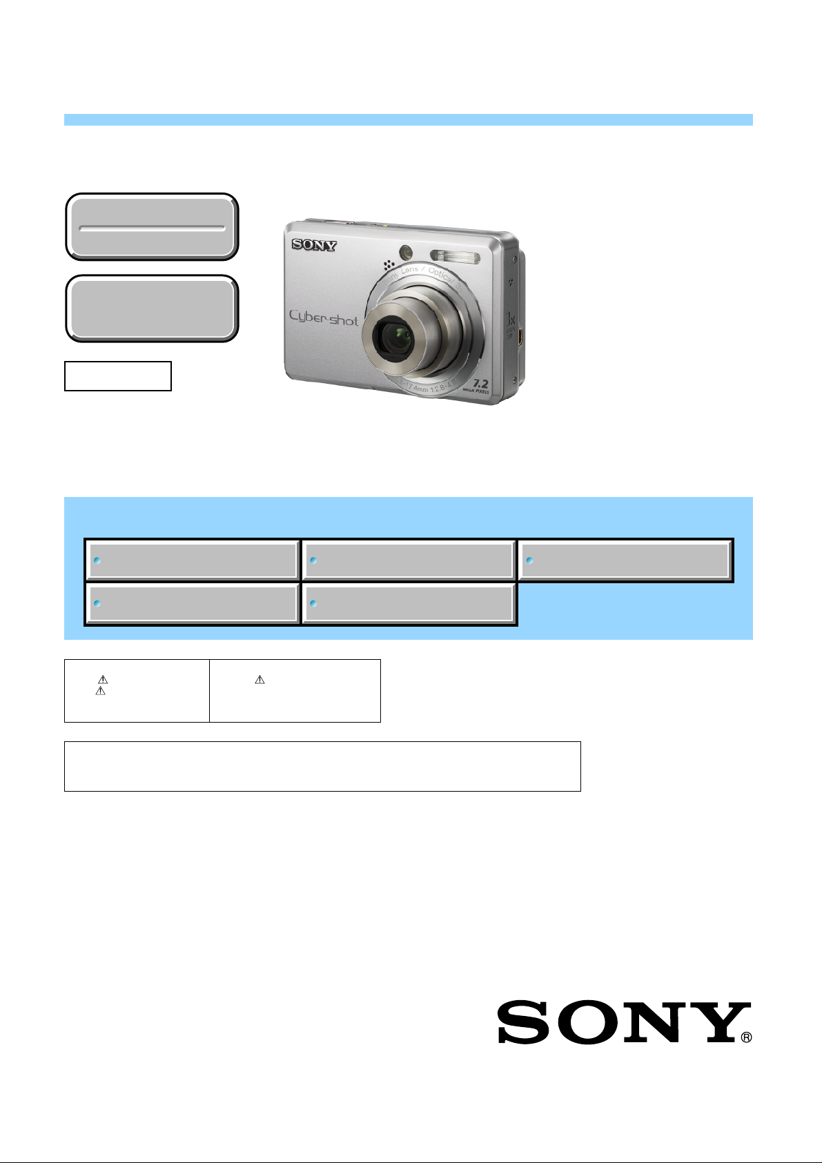
DSC-S730
US Model
Canadian Model
Ver. 1.1 2008.07
Revision History
Revision History
Internal memory
Internal memory
ON BOARD
ON BOARD
Revised-1
Replace the previously issued
SERVICE MANUAL 9-852-239-11
with this Manual.
Link
Link
SPECIFICATIONS
AEP Model
UK Model
E Model
Australian Model
Hong Kong Model
Chinese Model
Korea Model
Tourist Model
DISASSEMBLY REPAIR PARTS LIST
SERVICE NOTE
The components identified by
mark or dotted line with
mark are critical for safety .
Replace only with part number specified.
In case of the lens block assy, main board, or main frame assembly failure,
contact your local Sony Service Headquarter for the measures.
Les composants identifiés par une
marque sont critiques pour la
sécurité.
Ne les remplacer que par une pièce
portant le numéro spécifié.
BLOCK DIAGRAM
DIGITAL STILL CAMERA
DSC-S730
Sony EMCS Co.
2008G0200-1
© 2008.07
Published by Kohda TEC9-852-239-12
Page 2

SPECIFICATIONS
[System]
Image device: 7.20 mm (1/2.5 type) color CCD,
Primary color filter
Total pixel number of camera:
Approx. 7 410 000 pixels
Effective pixel number of camera:
Approx. 7 201 000 pixels
Lens: 3× zoom lens f = 5.8 – 17.4 mm (35 –
105 mm when converted to a 35 mm still
camera) F2.8 (W) – 4.8 (T)
Exposure control: Automatic exposure, Scene
Selection (7 modes)
White balance: Automatic, Daylight, Cloudy,
Fluorescent, Incandescent, Flash
File format (DCF compliant):
Still images: Exif Ver. 2.21 JPEG compliant,
DPOF compatible
Movies: AVI (Motion JPEG)
Recording media: Internal Memory (approx.
22 MB), "Memory Stick Duo"
Flash: Flash range (ISO sensitivity
(Recommended Exposure Index) set to Auto):
approx. 0.5 to 3.5 m (1 feet 7 3/4 inches to 11
feet 5 7/8 inches) (W)/approx. 0.5 to 2.0 m (1
feet 7 3/4 inches to 6 feet 6 3/4 inches) (T)
[Input and Output connectors]
(USB) A/V OUT terminal:
Video, Audio (Monaural), USB
communication
USB communication:
Hi-Speed USB (USB 2.0 compliant)
[LCD screen]
LCD panel: 6.0 cm (2.4 type) TFT drive
Total number of dots: 112 320 (480×234) dots
[Power, general]
Power: LR6 (size AA) Alkaline batteries (2), 3 V
HR15/51:HR6 (size AA) Nickel-Metal
Hydride batteries (2) (not supplied), 2.4 V
ZR6 (size AA) Oxy Nickel Primary Battery
(2) (not supplied), 3 V
AC-LS5K AC Adaptor (not supplied), 4.2 V
Power consumption (during shooting): 1.2 W
Operating temperature: 0 to 40 C (32 to 104 F)
Storage temperature: –20 to +60 C (–4 to +140
Dimensions: 91.4×61.0×29.1 mm (3 5/8×2 1/2×
1 3/16 inches) (W/H/D, excluding
protrusions)
Mass: Approx. 189 g (6.7 oz) (including two
batteries and strap, etc.)
Microphone: Monaural
Buzzer
Exif Print: Compatible
PRINT Image Matching III: Compatible
PictBridge: Compatible
Design and specifications are subject to change
without notice.
F)
DSC-S730
— 2 —
Page 3

Danger of explosion if battery is incorrectly replaced.
Replace only with the same or equivalent type.
CAUTION
SAFETY-RELATED COMPONENT WARNING!!
COMPONENTS IDENTIFIED BY MARK OR DOTTED LINE WITH
MARK ON THE SCHEMATIC DIAGRAMS AND IN THE PARTS
LIST ARE CRITICAL TO SAFE OPERATION. REPLACE THESE
COMPONENTS WITH SONY PARTS WHOSE PART NUMBERS
APPEAR AS SHOWN IN THIS MANUAL OR IN SUPPLEMENTS
PUBLISHED BY SONY.
SAFETY CHECK-OUT
After correcting the original service problem, perform the following
safety checks before releasing the set to the customer.
1. Check the area of your repair for unsoldered or poorly-soldered
connections. Check the entire board surface for solder splashes
and bridges.
2. Check the interboard wiring to ensure that no wires are
"pinched" or contact high-wattage resistors.
3. Look for unauthorized replacement parts, particularly
transistors, that were installed during a previous repair. Point
them out to the customer and recommend their replacement.
4. Look for parts which, through functioning, show obvious signs
of deterioration. Point them out to the customer and
recommend their replacement.
5. Check the B+ voltage to see it is at the values specified.
6. FLEXIBLE Circuit Board Repairing
Keep the temperature of the soldering iron around 270 C
during repairing.
Do not touch the soldering iron on the same conductor of the
circuit board (within 3 times).
Be careful not to apply force on the conductor when soldering
or unsoldering.
DSC-S730
ATTENTION AU COMPOSANT AYANT RAPPORT
À LA SÉCURITÉ!
LES COMPOSANTS IDENTIFÉS PAR UNE MARQUE SUR LES
DIAGRAMMES SCHÉMATIQUES ET LA LISTE DES PIÈCES SONT
CRITIQUES POUR LA SÉCURITÉ DE FONCTIONNEMENT. NE
REMPLACER CES COMPOSANTS QUE PAR DES PIÈSES SONY
DONT LES NUMÉROS SONT DONNÉS DANS CE MANUEL OU
DANS LES SUPPÉMENTS PUBLIÉS PAR SONY.
Unleaded solder
Boards requiring use of unleaded solder are printed with the leadfree mark (LF) indicating the solder contains no lead.
(Caution: Some printed circuit boards may not come printed with
the lead free mark due to their particular size.)
: LEAD FREE MARK
Unleaded solder has the following characteristics.
Unleaded solder melts at a temperature about 40 C higher than
ordinary solder.
Ordinary soldering irons can be used but the iron tip has to be
applied to the solder joint for a slightly longer time.
Soldering irons using a temperature regulator should be set to
about 350 C.
Caution: The printed pattern (copper foil) may peel away if the
heated tip is applied for too long, so be careful!
Strong viscosity
Unleaded solder is more viscous (sticky, less prone to flow) than
ordinary solder so use caution not to let solder bridges occur such
as on IC pins, etc.
Usable with ordinary solder
It is best to use only unleaded solder but unleaded solder may
also be added to ordinary solder.
— 3 —
Page 4

Ver. 1.1 2008.07
The changed portions from
Ver. 1.0 are shown in blue.
TABLE OF CONTENTS
Section Title Page
1. SERVICE NOTE
1-1. Process After Fixing Flash Error ·····································1-1
1-2. Method for Copying or Erasing the Data in Internal
Memory ···········································································1-1
2. DISASSEMBLY
2-1. Disassembly ·····································································2-1
3. BLOCK DIAGRAM
3-1. Overall Block Diagram ···················································3-1
4. REPAIR PARTS LIST
4-1. Exploded Views ·······························································4-1
4-1-1. Overall Section ······························································4-1
4-1-2. Main Frame Block ·························································4-2
4-1-3. Lens Block ····································································· 4-3
4-2. Accessories ······································································ 4-4
DSC-S730
— 4 —
Page 5

1. SERVICE NOTE
1-1. PROCESS AFTER FIXING FLASH ERROR
Method for Initializing the Flash Error
Initialize
Initializes the setting to the default setting.
Even if you execute this function, the images stored in the internal memory are retained.
1 Select [OK] with v on the control button, then press z.
The message "Initialize all settings Ready?" appears.
2 Select [OK] with v, then press z.
The settings are reset to the default setting.
To cancel initializing
Select [Cancel] in step 1 or 2, then press z.
Be sure not to power off the camera while initializing.
1-2. METHOD FOR COPYING OR ERASING THE DATA IN INTERNAL MEMORY
The data can be copied/erased by the operations on the Setup screen. (When erasing the data, execute formatting the internal memory.)
Note: When replacing the camera, erase the data in internal memory of the board before replacement.
Method for Copying the Data in Internal Memory
Copy
Copies all images in the internal memory to a "Memory Stick Duo".
1 Insert a "Memory Stick Duo" having sufficient free capacity.
2 Select [OK] with v on the control button, then press z.
The message "All data in internal memory will be copied Ready?" appears.
3 Select [OK] with v, then press z.
Copying starts.
To cancel copying
Select [Cancel] in step 2 or 3, then press z.
Use batteries with enough power remaining. If you attempt to copy image files using batteries with little
remaining charge, the batteries may run out, causing copying to fail or possibly corrupting the data.
You cannot select images to copy.
The original images in the internal memory are retained even after copying. To delete the contents of the
internal memory, remove the "Memory Stick Duo" after copying, then format the internal memory
([Format] in [Internal Memory Tool]).
A new folder is created on the "Memory Stick Duo" and all the data will be copied to it. You cannot
choose a specific folder and copy images to it.
The (Print order) marks on the images are not copied.
Method for Formatting the Internal Memory
DSC-S730
This item does not appear when a "Memory Stick Duo" is inserted in the camera.
Format
Formats the internal memory.
Note that formatting permanently erases all data in the internal memory, including even protected images.
1 Select [OK] with v on the control button, then press z.
The message "All data in internal memory will be erased Ready?" appears.
2 Select [OK] with v, then press z.
The format is complete.
To cancel formatting
Select [Cancel] in step 1 or 2, then press z.
1-1
Page 6

Y
The following flow chart shows the disassembly procedure.
2-1. DISASSEMBLY
2. DISASSEMBLY
2
5
1
4
1
Open the BT LID
2
SCREW M 1.7 X 2.7
3
SCREW TP 1.7 X 4
SCREW TP 1.7 X 3.5
4
CABINET (REAR) ASSY
5
3
SCREW TP 1.4 X 3.5
1
SCREW TP 1.4 X 4
2
LCD
3
4
LCD PLATE
4
3
2
1
DSC-S730
(To 2-2 Page)
1
BT LID SHAF T
2
BT LID
3
BT LID SPRING
2
3
1
2-1
Note :
When CABINET(FRONT) ASSY is
removed, the plate will bends if
CABINET(FRONT) ASSY is inclined
too much.
Please remove CABINET (FRONT)
ASSY as in parallel as possible.
plate
3
2
1
SCREW TP 1.4 X 3
1
2
SCREW TP 1.4 X 2.5
3
CABINET (FRONT) ASS
Page 7

Ver. 1.1 2008.07
The changed portions from
Ver. 1.0 are shown in blue.
(From 2-1 Page)
Caution
Shorting jig
(1kΩ / 1W)
Note :
After discharged, a transparent
seal is put again.
Do not lose the transparent seal
removed when discharged.
HELP01
HELP02
DSC-S730
HELP02
HELP01
HELP03
2-2
Page 8

Ver. 1.1 2008.07
HELP01
Be careful about the Lens Assy.
HELP
HELP02
Don't press the Barrier part.
Don't press the Sensor holder
Don't press the AF Motor
HELP03
Attach the Block assy protection sheet as shown.
Block assy
protection sheet
Keep clean these Pins.
Attach the Block assy
protection sheet avoiding
three screw holes.
DSC-S730
HELP
Page 9

Ver. 1.1 2008.07
The changed portions from
Ver. 1.0 are shown in blue.
3-1. OVERALL BLOCK DIAGRAM
3. BLOCK DIAGRAM
MAIN BOARD
STROBE & TOP BOARD
OP
T
U
T
SH
VD
TOP
POWER LED
1
FL AS H
ND
FL AS H
SHU
PW_LE
PWR_KE Y
GREEN
ASH
FL
FLASH_CHG_
S
TROBE_TR
O
BE_CH
R
AF_L
ROBE_P
ST
1
2
T
D
2
Q5
D
_
Y
R
L
G
G
ED
WR
+3.1VD
D
DGN
FLASH _V P
_
ST RO
CH
BE
G
STRO
rg
B
E_T
FLASH_R D
Y
SELF TIMER LED
1 2
GREEN
FLASH _V P
+5
VM
+
.1VD
3
DG ND
+3.1
DGND
FLASH
CHARGER
FLASH_VP
+5
VM
+3.1VDST
DG
LCD
AUO LCD
2.36
INCH
PANEL
LCD_BACKLIGHT
1
2
D
D
E
E
R
R
1
SHUT
HUT2
S
D
PW_LE
R_K
PW
Y
E
+2.5V
D
D
4
2
1
1
P1,P2
,
NC
S
S
3
CAPACITOR
100UF 300V
FLASH_RDY
FLAS H_CH G_L
ST ROBE_TR G
E
TR OB
CH G
S
_
F_ LE D
A
B
E_PW
STRO
FLASH TUBE
2
3
1
Q2
2
R
GN D
+2
DGND
LCD
DD
VD
.5
D
+3
LCD_EN
LCD
_MCL
LCD_V
LCD_HD
CD_SCLK
L
LCD_SDATA
LCD
MLC
R
RAM
D[0
RAMA[0..14]
RA
RAMWE_N
RAM
RAM
R
AMCS_
R
AMLDQ
M
RA
RAMUD
RAMCLK_N
AM
R
RAMCLK_EN
RAMRE
R
D
+
5VM
VM
+5
+
D
3.1V
.1VD
[
..7
0
D_ON
D
GND
..1
M
L
CAS
RAS
UD
CLK
CD_
L
N
E
LCD_EN
LCD_MCLK
K
LC
D
B
5
DM
N
S
S
Q
M
D_
CD_HD
L
CD _SCLK
L
L
C
D_SDAT
L
CD
]
C
L
M
D_ON
L
D
GN
D
AMD[
15]
0..
R
]
[
]
R
0..1
AMA
4
A
MLDM
R
RAMWE_
N
A
A
R
C
M
S
R
A
S
RAM
R
AMC
S_N
Q
AML D
R
S
R
Q
S
AMUD
RAMUDM
N
RAMCLK_
LK
RAM
C
E
R
AMCLK_
N
R
AMRE
F
F
K
LCD_MCL
D
V
LCD_VD
LCD
HD
_
LCD_SCLK
A
LC
DAT
D_S
A
]
[
0..7
LCD[0..7
]
M
LCD_ON
B
L
BL
SHUT1
SH
2
UT
PW
_LED
R_KEY
PW
0..
RAMD[
1
]
5
A
]
R
0..1
MA[
4
M
A
R
MLD
RAMWE_N
S
RAMCA
RA
M
RAS
RA
MCS_
N
RAMLDQ
S
S
RA
Q
MUD
RA
MUDM
RAMCLK_N
L
RA
K
MC
RA
MCLK_EN
RAMREF
F
LASH_RDY
FLASH_CHG_L
G
STROBE
_TR
STROBE
H
_
G
C
AF_LE D
ST
BE
R
_
O
PWR
MODE DIAL
FUNCTION KEY
MS LED
1 2
GREEN
SW
VP
-7.5V
+2.5VD
+3.3V
+3.1VD
+5V M
+13.4V
+1.8VD
+3.1VD
DG
ND
STA_LED
SW_
KEY_
SW_KEY_AD C
SW
VP
-7.5V
+2.5VD
+3.3V
+3.1VD
+5
VM
V
+13.4
+1.8VD
VD
+3.1
D
DGN
ADC
PO WE R
POWER
1
CC D_ON1
PWR_C TRL
CCD_ON
Q29
AO3415
SW_KEY_AD C1
SW_K
DGN
D
STA_LE D
EY _A DC
12MHZ
CCD_
DG ND
12
C
D_O N1
C
PWR_CTRL
ON
+1.8VD
+3.1V
+3.3VS
+3.3V
+2.5VD
DG ND
VP
D
STA_LED
SW_KEY_AD C
SW_K
EY_ADC
CC D_ON1
PWR_C TRL
VP
+1.8VD
+3.1VD
VS
+3.3
3.3
+
V
+2.5VD
DGND
DSP
1
DSP
PXCL
DS_EN
C
SC
SD
AT
AFE RST
TG_EN
VSUB_Co
_Con2
VS
UB
CC
D_O
G_ON
T
S_
C
D
CC D[0..11]
M
S_ON
MS_INS
C
AL
C
MS_CLK
MD[0
FA23
FA20
F
FA2
PER
BEE
LENS_PS
S
HUTTER_
SH
UTTER_M
L
ENS_
LENS_SC LK
LENS_SD ATA
ZOOM_PI
ZOOM_PR
FOCUS_PI
PWR_ON
PWRKEY
BAT_LO
USB_DET
AV_DE T
VIDEO_OUT
LINE_OUT
BEE P
SW_PLAYBAC
SW_W IDE
SW_TEL
MIC
MIC_N
PXCL
2
2
.768KHz
.768KHz
3
3
2
H
D
V
D
CD
S_E
SCLK
S
AT A
D
AF ERST
T
G_EN
VS UB_Con
UB
V
S
C
D_O
C
TG _
O
CDS_ON
[
CCD
MS_O N
R
/B
MS_ INS
C
LE
WE
WP
ALE
0
CE
RE
MS
_CL
[
M
0
..7
D
F
3
A
2
0
FA2
2
F
2
A
FA2
1
BE EPER
LE NS _P S
HUT T ER_M
S
SHUTTER_M0
IN1
IN2
3
IN
IN
4
LEN
S_EN
LEN
S_SCLK
ENS_SDATA
L
ZOOM_PI
ZO OM_P R
FO C US _PI
PW R_ON
PW RK E Y
BAT_LOA
D+
-
D
US B_ DE T
AV _D ET
VIDEO_ OU T
INE _OUT
L
EE P E
B
R
SW_PLAYBACK
SW _WIDE
SW _T E L
4
1
3
K
N
1
2
_Con
N
N
]
..11
0
D
GN D
+3.1VD
#
K
]
+3.1VD
1
+5
VM
DGND
D
E
K
HD
VD
LK
A
n1
N
N
O
B
R/
#
LE
WE
WP
E
E0
E
R
..7]
A22
1
M1
0
N1
I
IN2
I
N3
IN4
EN
AD
D+
D
-
ER
K
E
13
BATT+2
BATT-2
R
7X_V
52
1
1
_
K
C187
P00
01
2
2
R
1
7X_V
X_V
1
52
52
C159
2
_
_
K
K
2
P00
P00
01
01
2
R
R
5X
5X
_V6
_V6
1_KU1.
1_KU1.
C186
0
0
R
5
X_V
61
_K
U
1
.
0
Q42
AO3415
13
2
C160
12
R131
100K
F5 1A/30V
12
12
F3 1.6A/36V
-7.5V
12
R163
100K
-7.5V
FLASH_VP
VP
PXCLK
D
H
VD
CDS_E
N
K
SCL
SDATA
AF
ST
E
R
G
_
T
EN
VSUB_C o
VSUB_Co
C
N
D_O
C
N
T
G_O
DS_O
N
C
0..11
CCD[
ME MO RY
G
ND
D
3
+
1VD
.
S_ON
M
R/B
I
S_
M
NS#
E
L
C
E
W
W
P
AL
E
CE
0
RE
MS_CLK
M
D[0..7]
FA23
A2
F
0
FA22
F
A21
MEMO
VD
+3.1
ENS_PS
L
TTER
SHU
SHUTTER_M0
I
N1
N2
I
IN3
N4
I
S_
EN
LEN
LENS_SC LK
LENS_SD ATA
OM_
ZO
PI
ZOOM_PR
FOC US_
+5VM
DGND
D+
D-
A/V_DE T
VIDEO_O
INE_OUT
L
EE PE
B
R
C
D
1
n
n2
]
CD S
LENS
_M1
PI
LE NS
JACK
UT
JAC
S
+13.4V
Y
R
+3.1VDUSB_DE T
K
314 256
+
DG
DGND
UGND
3
V
3.
-
7.5V
ND
+3.1VD
+3
V
.3
-
V
7.5
3.4
+
V
1
DGND
12
+3.1VD
DG ND
UGND
56
3 1
4 2
4
GND_3
Out
Power
1
GND_2
MIC1
MIC1
SP M02 04HD5
SP M02 04HD5
MC4_4.72X3.76_173
G2412-0039-00
33.75MHZ
314 2
1
V
3.
+
4
56
3
2
LENS BLOCK
LENS
IRIS(METER)
MEMORY STICK
BUZZER
ZOOM SENSOR
ZOOM MOTOR
FOCUS SENSOR
FOCUS MOTOR
IRIS MOTOR
SHUTTER MOTOR
PC
DSC-S730
3-1
Page 10

Ver. 1.1 2008.07
The changed portions from
V er. 1.0 are shown in blue.
4-1. EXPLODED VIEWS
4-1-1. OVERALL SECTION
ns: not supplied
4. REPAIR PARTS LIST
12
11
13
3
15
4
ns
Q1
6
16
18
2
19
10
5
(Note)
17
7
ns
1
• Refer to cover for mark .
Ref. No. Part No. Description
1X-2188-411-1
2X-2188-412-1
33-286-696-01 SHAFT, STRAP
43-286-697-01 BLOCK, RL
53-286-698-01 LCD
6A-1444-049-A ST BLOCK ASSY
73-286-700-01 SHAFT, BT LID
8 3-286-701-01 LID, BT
9 3-286-702-01 SPRING, BT LID
10 3-286-703-01 LID, JACK
15
9
8
CABINET (FRONT) ASSY
CABINET (REAR) ASSY
14
Main Frame Block
(See Page 4-2)
Note : The adjustment is not required after replacing the LCD
Ref. No. Part No. Description
11 3-287-023-11 SCREW M1.7 X 2.7
12 3-287-026-01 SCREW TP1.4 X 2.5
13 3-287-028-01 SCREW TP1.7 X 3.5
14 3-287-027-01 SCREW TP1.7 X 4
15 3-287-025-01 SCREW TP1.4 X 3
16 3-287-032-01 SCREW TP1.7 X 6.5
17 3-296-920-01 SCREW TP1.4 X 3.5
18 3-296-921-01 SCREW TP1.4 X 4
19 3-299-366-01 SCREW TP1.7 X 3.5
Q1 4-107-819-01 TRANSISTOR FLASH STROBOSCOPE
DSC-S730
4-1
Page 11

Ver. 1.1 2008.07
The changed portions from
Ver. 1.0 are shown in blue.
4-1-2. MAIN FRAME BLOCK
ns: not supplied
4. REPAIR PARTS LIST
Lens Block
(See page 4-3)
(Note 2)
ns
105
106
102
R82
(Note 3)
F5
F3
102
Q16
(Note 3)
104
(Note 1)
ns
102
103
107
101
Note 1 : In case of main board failure, contact your local Sony
service Headquarter for the measures.
• Refer to cover for mark .
Ref. No. Part No. Description
101 3-286-699-01 SUPPORT (JACK)
102 3-287-024-01 SCREW TP1.4 X 3
103 3-287-026-01 SCREW TP1.4 X 2.5
104 3-287-028-01 SCREW TP1.7 X 3.5
105 3-286-704-01 FRAME, MAIN
106 X-2319-399-1 BASE, BT
Note 2 : When separate lens block assy and main board for
main frame replacement, assemble original lens block
assy and main board back after repaire.
Note 3 : Refer to "Installation position of Q16 and R82" for
the installation position of Q16 and R82.
• Items marked “*” are not stocked since they are seldom required for
routine service. Some delay should be anticipated when or
dering these items.
Ref. No. Part No. Description
*
107 1-820-333-11 MULTI CONNECTOR (REC) 8P
F3 1-576-913-11 FUSE, MICRO (1608 TYPE) (1.6A/36V)
F5 1-576-363-11 FUSE, MICRO (1005 TYPE) (1A/30V)
TRANSISTOR DTC144WM3T5GQ16 4-120-071-01
R82 1-218-957-11 RES-CHIP 2.2k 5% 1/16W
DSC-S730
4-2
Page 12

Ver. 1.1 2008.07
4-1-3. LENS BLOCK
ns : not supplied
4. REPAIR PARTS LIST
153
ns
(CCD Assy)
(Note)
151
152
ns
(TP1.4X3)
Note : In case of the CCD assy failure, contact your local Sony
service Headquarter for the measures.
DSC-S730
Ref. No. Part No. Description
151 A-1444-054-A LENS BLOCK ASSY
152
153
4-110-079-01 FILTER SET, LOW PASS
4-110-077-01 SHEET, BLOCK ASSY PROTECTION
4-3
Page 13

4-2. ACCESSORIES
Checking supplied accessories.
A/V cable
3-196-980-01
4. REPAIR PARTS LIST
Note 1: This item is supplied with the unit as an accessory,
but is not prepared as a service part.
USB cable
3-196-981-01
Wrist strap
2-050-981-01
LR6 (size AA) Alkaline Battery
(Note 1)
CD-ROM
(Cyber-shot application software/
"Cyber-shot Handbook"/
"Cyber-shot Step-up Guide")
*3-281-189-01
Instruction Manual
3-281-198-11 (ENGLISH) (CND, AEP, UK, E, AUS, HK, JE)
3-281-198-21 (FRENCH, ITALIAN) (CND, AEP)
3-281-198-31 (SPANISH, PORTUGUESE) (AEP, E, JE)
3-281-198-41 (GERMAN, DUTCH) (AEP)
3-281-198-51 (TRADITIONAL CHINESE, SIMPLIFIED CHINESE) (E, HK, JE)
3-281-198-61 (RUSSIAN, UKRAINIAN) (AEP)
3-281-198-71 (ARABIC, PERSIAN) (E)
3-281-198-81 (KOREAN) (KR, JE)
3-281-198-91 (POLISH, CZECH) (AEP)
3-281-199-11 (HUNGARIAN, SLOVAK) (AEP)
3-281-199-21 (SWEDISH, FINNISH) (AEP)
3-281-199-31 (NORWEGIAN, DANISH)(AEP)
3-281-199-41 (THAI, MALAYSIAN) (E)
3-281-199-51 (TURKISH, GREEK) (AEP)
3-281-199-61 (ENGLISH, SPANISH) (US)
3-281-199-71 (SIMPLIFIED CHINESE) (CH)
Cyber-shot Handbook(PDF)
The CD-ROM supplied contains all of language version of
the Instruction Manual in pdf (Cyber-shot Handbook.pdf) for printing.
The printed matter is not supplied. If required,
please order it with the part number below.
* 3-281-190-11 (ENGLISH)
* 3-281-190-21 (FRENCH)
* 3-281-190-31 (ITALIAN)
* 3-281-190-41 (SPANISH)
* 3-281-190-51 (PORTUGUESE)
* 3-281-190-61 (GERMAN)
* 3-281-190-71 (DUTCH)
* 3-281-190-81 (TRADITIONAL CHINESE)
* 3-281-190-91 (SIMPLIFIED CHINESE)
* 3-281-191-11 (RUSSIAN)
* 3-281-191-21 (ARABIC)
* 3-281-191-31 (PERSIAN)
* 3-281-191-41 (KOREAN)
* 3-281-191-51 (POLISH)
* 3-281-191-61 (CZECH)
* 3-281-191-71 (HUNGARIAN)
* 3-281-191-81 (SLOVAK)
* 3-281-191-91 (SWEDISH)
* 3-281-192-11 (FINNISH)
* 3-281-192-21 (NORWEGIAN)
* 3-281-192-31 (DANISH)
* 3-281-192-41 (THAI)
* 3-281-192-51 (MALAYSIAN)
* 3-281-192-61 (TURKISH)
* 3-281-192-71 (GREEK)
* 3-281-192-81 (UKRAINIAN)
NOTE:
DSC-S730
Items marked “*” are not stocked since they are seldom required for routine service.
Some delay should be anticipated when ordering these items.
Abbreviation
AUS : Australian model
CH : Chinese model
CND : Canadian model
HK : Hong Kong model
JE : Tourist model
KR : Korea model
4-4
Page 14

Ver. 1.1 2008.07
【
Installation position of Q16 and R82
】
R82 1-218-957-11 2.2K 5% 1/16W
Q16 4-120-071-01 DTC144WM3T5G
MAIN BOARD
・
R82
Q16
DSC-S730
Page 15

Ver. 1.1 2008.07
The changed portions from
Ver. 1.0 are shown in blue.
【
Regarding Fuse
MAIN BOARD
・
】
F5
F3
DSC-S730
F3
F5
Ref. No. : F5
Part No. : 1-576-363-11
Description : FUSE, MICRO (1005 TYPE) (1A/30V)
Ref. No. : F3
Part No. : 1-576-913-11
Description : FUSE, MICRO (1608 TYPE) (1.6A/36V)
Page 16

Reverse
985223912.pdf
Revision History
Ver.
1.0
1.1 2008.07 Revised-1 • Addition of DISASSEMBLY for Lens Assy
Date
2007.11
History
Official Release
Contents
—
• Addition of HELP
• Change of BLOCK DIAGRAMS
• Addition of REPAIR PARTS LIST
• Addition of
Installation position of Q16 and R82
• Revision of Regarding Fuse
S.M. Revised :
Page 4, 2-2, HELP, 3-1, 4-1, 4-2, 4-3,
Installation position of Q16 and R82,
Regarding Fuse
S.M. Rev.
issued
—
Yes
DSC-S730
 Loading...