

Sony DR-BT1,DR-BT1K Service Manual
DR-BT1/BT1K
US Model
SERVICE MANUAL
BLUETOOTH EARSET SYSTEM
SPECIFICATIONS
Ver. 1.1 2005.01
Sony Corporation
Personal Audio Company
Published by Sony Engineering Corporation
9-879-223-02
2005A02-1
© 2005.01
General
Bluetooth Compliance: Bluetooth standard Ver. 1.1
Output power: Bluetooth standard Power Class2
Frequency band: 2.4GHz band ( 2.4000 GHz – 2.4835
GHz )
Max. Communication range:
Line of sight approx. 10 m
Supplied accessory: AC power adaptor (1),
Hanger (S) (1), Car attachment (1)
Battery charger (1) (BT1 only)
Bluetooth earset DR-BT1
Supported Bluetooth Profiles:
Headset Profile, Hands-free Profile
Power source: DC 3.7 V: Built-in Li-ion rechargeable
battery
Typical Talk time: 7 hours
Typical Standby Time: 160 hours
Mass: Approx. 20 g
Receiver
Type: Open air, dynamic
Driver unit: 13.5 mm dome type (CCAW Voice
Coil)
Sensitivity: 104 dB/mW
Impedance: 16 Ω at 1 kHz
Power handling capacity: 50 mW (IEC)
Reproduction frequency range:
50 – 20,000 Hz
Microphone
Type: Flexible pipe microphone
Unit: Electret condenser
Output impedance: Under 2.2 kΩ
Open circuit voltage level: -42 dB(0 dB = 1 V/Pa)
Effective frequency range: 100 – 5,000 Hz
Bluetooth earset adaptor DRC-BT1 (BT1K only)
Supported Bluetooth Profiles:
Headset Profile
Power source: DC 1.2 V: Built-in Ni-MH rechargeable
battery
Typical Talk time: 5 hours
Typical Standby Time: 100 hours
Cord: 0.20 m (Max. stretch length 0.7m)
Plug: 2.5 mm tri-pole plug
Mass: Approx. 35 g (without cord)
Design and specifications are subject to change without notice.
Photo : DR-BT1K

DR-BT1/BT1K
2
TABLE OF CONTENTS
Notes on chip component replacement
• Never reuse a disconnected chip component.
• Notice that the minus side of a tantalum capacitor may be
damaged by heat.
Unleaded solder
Boards requiring use of unleaded solder are printed with the lead
free mark (LF) indicating the solder contains no lead.
(Caution: Some printed circuit boards may not come printed with
the lead free mark due to their particular size.)
: LEAD FREE MARK
Unleaded solder has the following characteristics.
• Unleaded solder melts at a temperature about 40°C higher
than ordinary solder.
Ordinary soldering irons can be used but the iron tip has to
be applied to the solder joint for a slightly longer time.
Soldering irons using a temperature regulator should be set
to about 350°C.
Caution: The printed pattern (copper foil) may peel away if
the heated tip is applied for too long, so be careful!
• Strong viscosity
Unleaded solder is more viscous (sticky, less prone to flow)
than ordinary solder so use caution not to let solder bridges
occur such as on IC pins, etc.
• Usable with ordinary solder
It is best to use only unleaded solder but unleaded solder
may also be added to ordinary solder.
1. SERVICING NOTES........................................................ 3
2. GENERAL ........................................................................... 3
3. DIAGRAMS
3-1. Block Diagrams ···························································· 5
3-2. Printed Wiring Boards – Headset Board– ···················· 6
3-3. Schematic Diagram – Headset Board– ························ 7
3-4. Printed Wiring Boards
– Adaptor Board (BT1K only)– ·································· 8
3-5. Schematic Diagram – Adaptor Board (BT1K only)–··· 9
3-6. Printed Wiring Boards
– Charger Board (BT1 only)– ··································· 10
3-7. Schematic Diagram – Charger Board (BT1 only)–···· 11
4. EXPLODED VIEWS
4-1. Headset Section ·························································· 12
4-2. Adaptor Section (BT1K) ············································ 13
4-3. Charger Section (BT1) ··············································· 14
5. ELECTRICAL PARTS LIST........................................ 15
• MOD2 (bluetooth module), IC7 (+2.8V REG) on
HEADSET board cannot be replaced individually.
Replace it with “HEADSET BOARD, COMPLETE”.
• MOD1 (bluetooth module) on ADAPTOR board cannot be
replaced individually.
Replace it with “ADAPTOR BOARD, COMPLETE”.
DR-BT1/BT1K
3
SECTION 1
SERVICING NOTES
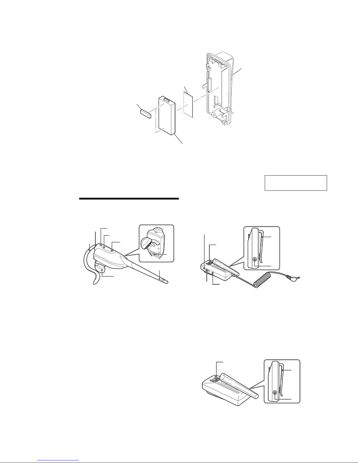
In case of replacing a nickel hydrogen battery in the adaptor (BT-1K), replace two battery pads and a battery sheet at the same time.
two battery pads
battery sheet
cabinet (lower
)
nickel hydrogen battery
SECTION 2
GENERAL
This section is extracted
from instruction manual.
Identifying
Bluetooth earset
R
L
1
23
4
5
6
7
8
1 Hanger
2 Multifunction button
Controls various functions of the Bluetooth earset.
3 LED indicator
Indicates the status of the Bluetooth earset.
4 VOLUME +
5 VOLUME -
6 Pipe microphone
7 Housing
8 Contact terminals
Bluetooth earset adaptor (BT1K only)
1
3
4
5
6
2
1 LED indicator
Indicates the status of the Bluetooth earset adaptor.
2 Power on button
3 Pairing / Power off button
4 Contact pins
5 Belt clip
6 DC IN 4.5 V jack
Battery charger (BT1 only)
1
2
3
1 Contact pins
2 Belt clip
3 DC IN 4.5 V jack

DR-BT1/BT1K
4
SECTION 3
DIAGRAMS
For schematic diagrams.
Note:
• All capacitors are in µF unless otherwise noted. (p: pF)
50 WV or less are not indicated except for electrolytics
and tantalums.
• All resistors are in Ω and 1/4 W or less unless otherwise
specified.
•%: indicates tolerance.
• C : panel designation.
• A : B+ Line.
• Power voltage are dc 3.7 V (Headset) or dc 1.2 V (Adaptor) and fed with regulated dc power supply from battery
terminal.
•Voltages are dc with respect to ground under tolerances.
no mark : STANDBY
(): TALKING
<>: AC ADAPTOR IN
•Voltages are taken with a VOM (Input impedance 10 MΩ).
Voltage variations may be noted due to normal production tolerances.
• Signal path.
F : AUDIO
NOTE FOR PRINTED WIRING BOARDS AND SCHEMATIC DIAGRAMS.
Caution:
Parts face side: Parts on the parts face side seen from
(Side A) the parts face are indicated.
Pattern face side: Parts on the pattern face side seen from
(Side B) the pattern face are indicated.
For printed wiring boards.
Note:
• X : parts extracted from the component side.
• Y : parts extracted from the conductor side.
• : Pattern from the side which enables seeing.
(The other layers' patterns are not indicated.)
• MOD2 (bluetooth module), IC7 (+2.8V REG) on HEADSET board
cannot be replaced individually.
Replace it with “HEADSET BOARD, COMPLETE”.
• MOD1 (bluetooth module) on ADAPTOR board cannot be replaced
individually.
Replace it with “ADAPTOR BOARD, COMPLETE”.
• MOD2 (bluetooth module), IC7 (+2.8V REG) on HEADSET board
cannot be replaced individually.
Replace it with “HEADSET BOARD, COMPLETE”.
• MOD1 (bluetooth module) on ADAPTOR board cannot be replaced
individually.
Replace it with “ADAPTOR BOARD, COMPLETE”.
• HEADSET board is four-layer pritnted board.However, the patterns
of flayer 2 and 3 have not been included in this diagrams.
DR-BT1/BT1K
55
DR-BT1/BT1K
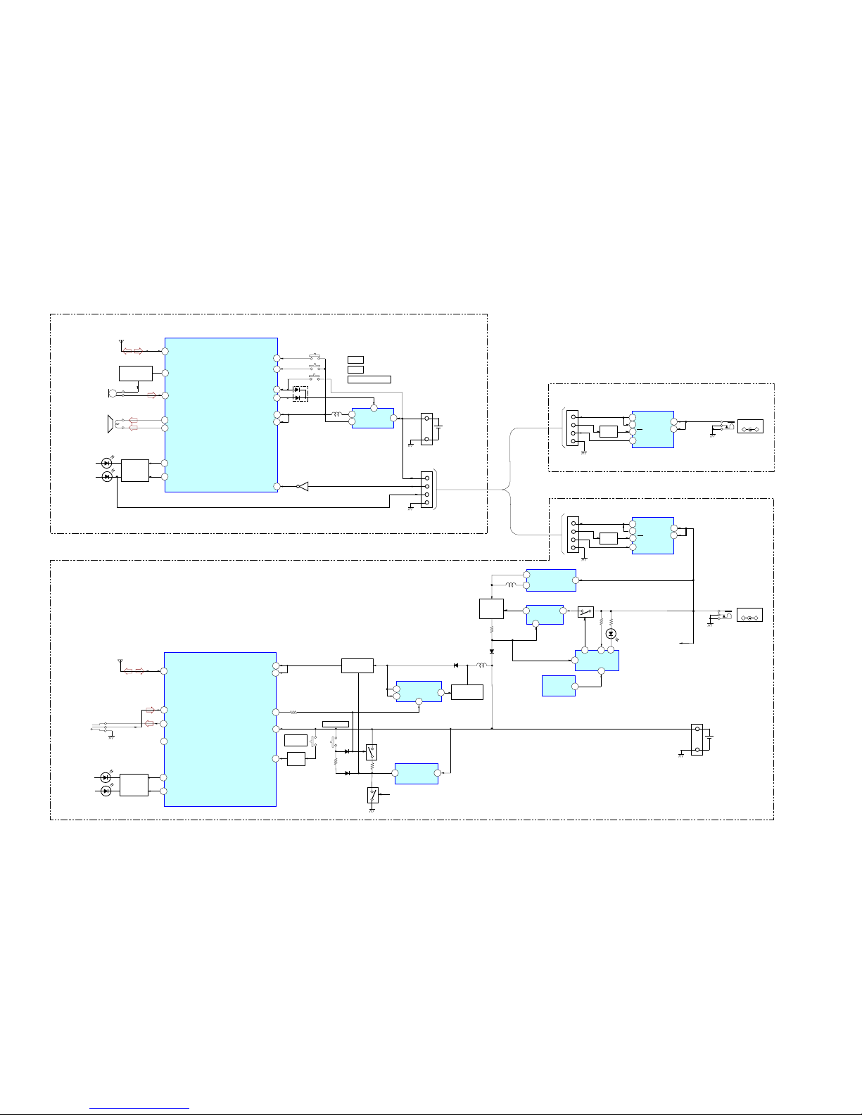
3-1. BLOCK DIAGRAM
• Signal path
F : AUDIO
D10
(BLUE)
PIO1
10
14
2
23
3
1
2
+1.5V REG.
IC3
29
MIC1
MIC
ANT
INH
IC2
BATT
30
ANT2
ANTENNA
SPEAKER
6
3
1
2
7
8
CHGN
MIC_N
PIO0
VDD_IO
RESETB
DC/DC CONVERTER
IC9
5
1
4
CN2
IC4
1 2
SP1
S4
MULITI FUNCTION
4
3
LED DRIVER
Q16
D11
(GREEN)
26
15
24
PIO4
IC7
PIO3
3
4
22
6
1
+2.8V REG.
D9
PIO5
S3
VOL +
S2
VOL -
P1O9
VREG_IN
CHARGE
TERMINAL
RECHAGEABLE
BATTERY (LI-ION)
3.7V
1
2
3
4
B2
Q14
INV.
Q15
DELAY SWITCH
1
PIO11
MOD2
RECEIVER/TRANSMITTER,
MIC AMP,AF AMP,
BLUETOOTH CONTROL
SPKR_P
SPKR_N
PIO10
10
29
2
25
ANT
1
ANT1
ANTENNA
5
MIC_P
PIO11
VDD_IO
CN1
3
LED DRIVER
Q8
11
POWER ON
IC5
6
1
2
DC/DC CONVERTER
+B SWITCH
Q4,5
Pairing/
Power off
PIO9
PIO1
BATTERY
LEVEL DETECT
RECHARGEABLE
BATTERY (NI-MH)
1.2V
B1
28
PIO2
MOD1
RECEIVER,TRANSMITTER
MIC AMP,AF AMP,
BLUETOOTH CONTROL
SPKR_P
P1
PHONE MIC_P
PHONE SPKR_P
(PHONE PLUG)
Q17,18
BUFFER
CN3
4
SWITCHING
Q6
IC1
3
STAT1
IC6
BATT
9
1
2
7
3
OUT
LI-ION BATTERY
CHARGE MANAGEMENT
TEMPERATURE
DETECT
TIME LEDN
D8
(CHARGE)
BATTERY
CHARGER
J1
DC IN 4.5V
10
BUFFER
Q13
CE
IN
VCC
1
2
3
4
1
2
3
4
CN3
STAT1
IC6
BATT
9
1
2
7
3
OUT
LI-ION BATTERY
CHARGE MANAGEMENT
10
BUFFER
Q13
SE
IN
VCC
(BT1K ONLY)
ADAPTOR
HEAD SET
J1
DC IN 4.5V
Q1,3
(BT1 ONLY)
CHARGER
D5
(BLUE)
D6
(GREEN)
S1
S5
D7
D4
Q7(2/2)
Q7(1/2)
14
VDD_IO
15
VREG_IN
D3
D2
CURRENT
CONTROL
Q2
+VB
+VB
-
+
-
+
DR-BT1/BT1K
66
DR-BT1/BT1K
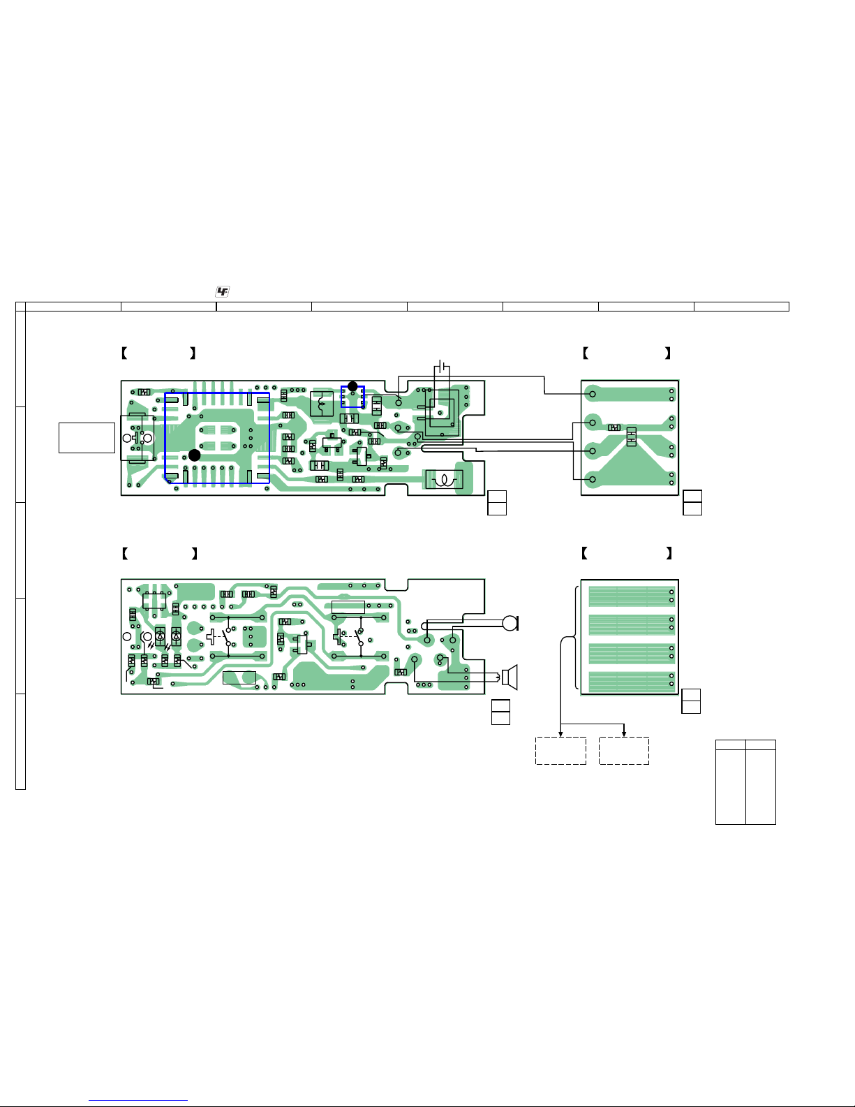
3-2. PRINTED WIRING BOARD – HEADSET BOARD –
: Uses unleaded solder.
Ref. No. Location
D9 D-3
D10 D-2
D11 D-2
IC7 A-4
MOD2 B-2
Q14 B-4
Q15 B-4
Q16 D-2
• Semiconductor Location
HEADSET BOARD
11
(11)
1-864-044-
11
(11)
1-864-044-
11
(11)
1-864-046-
11
(11)
1-864-046-
(
SIDE A
)
HEADSET BOARD
CONNECTOR BOARD
(
SIDE A
)
CONNECTOR BOARD
(
SIDE B
)(
SIDE B
)
1
1
2
8
9
15
1623
24
30
E
E
136
4
1
534
C23
R43
D9
S3
R50
D11
C24
R47
R49
R48
R38
R42
C33
R41
D10
R46
Q16
R63
MIC1
SP1
SPEAKER
C34
L5
L6
C27
IC7
C20
C19
L2
MOD2
C22
R39
R44
C21
ANT2
R55
R45
R40
S2
C25
R56
C38
C40
C35
CN2
Q15
Q14
R64
C53
MULTI
FUNCTION
B2
RECHARGEABLE
BATTERY(LI-ION
)
+
3.7V
E
VOL
+
S4
VOL
-
ADAPTOR
(Page 8)
BT1K
CHARGER
(Page 10)
BT1
2
3 4 5 6 7
8
A
1
B
C
D
E
 Loading...