Sony DPIF-5100 Service manual
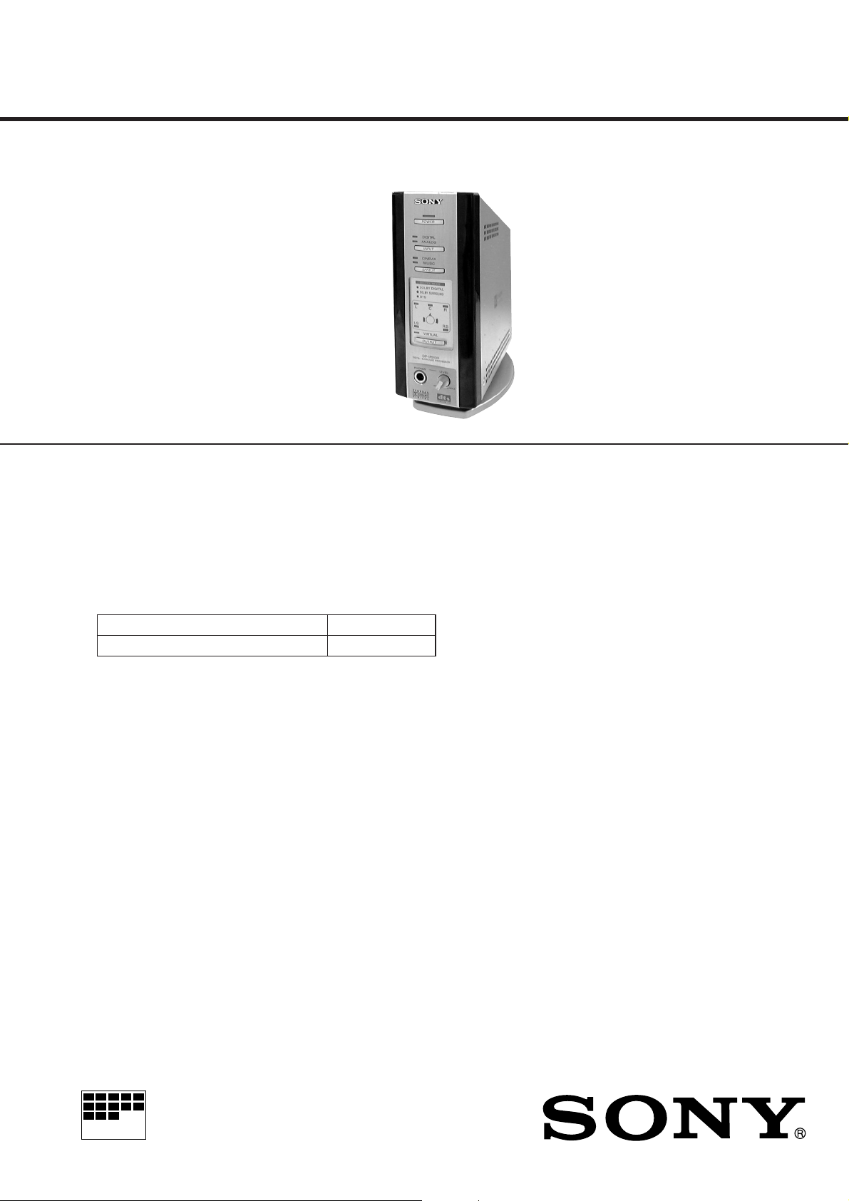
DP-IF5100
SERVICE MANUAL
Ver 1.0 1999. 10
Manufactured under license from Dolby Laboratories Licensing
•
Corporation.
DOLBY, the double-D symbol ; , “PRO LOGIC”,
“Dolby Digital (AC-3)”, and “VIRTUAL DOLBY DIGITAL” are
trademarks of Dolby Laboratories Licensing Corporation.
DP-IF5100 is the component model block one in
•
MDR-DS5100.
COMPONENT MODEL NAME FOR MDR-DS5100
DIGITAL SURROUND PROCESSOR DP-IF5100
CORDLESS STEREO HEADPHONES MDR-IF5000
E Model
SPECIFICATIONS
Modulation System Frequency modulation
Carrier wave frequency Right channel 2.8 MHz
Left channel 2.3 MHz
Transmission distance Approx. 10 m to the front
Transmission range 20 – 20,000 Hz
Distortion rate 1% or less (1 kHz)
Audio inputs Optical input
(rectangular-type) × 1
Analog input (pin jack
left/right) × 1
Power requirements DC 9 V (from the
supplied AC power
adapter)
Dimensions (w/h/d) Approx. 85 × 190 × 180
mm (3 3/8 × 7 1/2 × 7 1/8
inch)
Mass Approx. 1.0 kg
(1000 g) (2 lb 30 oz)
MICROFILM
Design and specifications are subject to
change without notice.
Notes on Chip Component Replacement
• Never reuse a disconnected chip component.
• Notice that the minus side of a tantalum capacitor may be dam-
aged by heat.
DIGITAL SURROUND PROCESSOR
– 1 –

TABLE OF CONTENTS
1. GENERAL
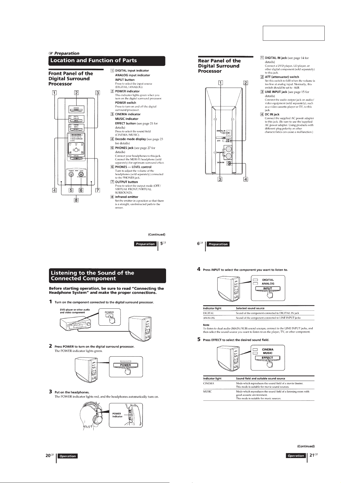
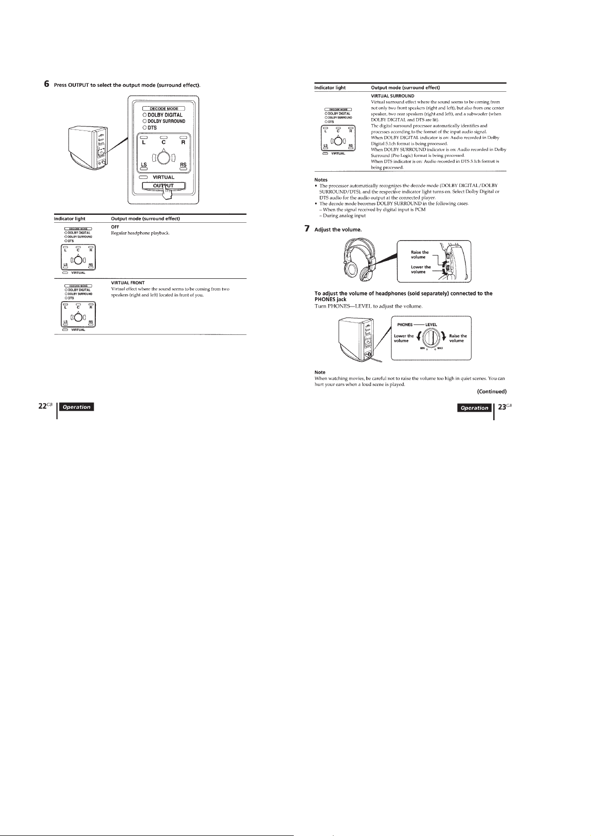
Location and Function of Parts............................................... 3
Listening to the Sound of the Connected Component............ 3
2. DISASSEMBLY
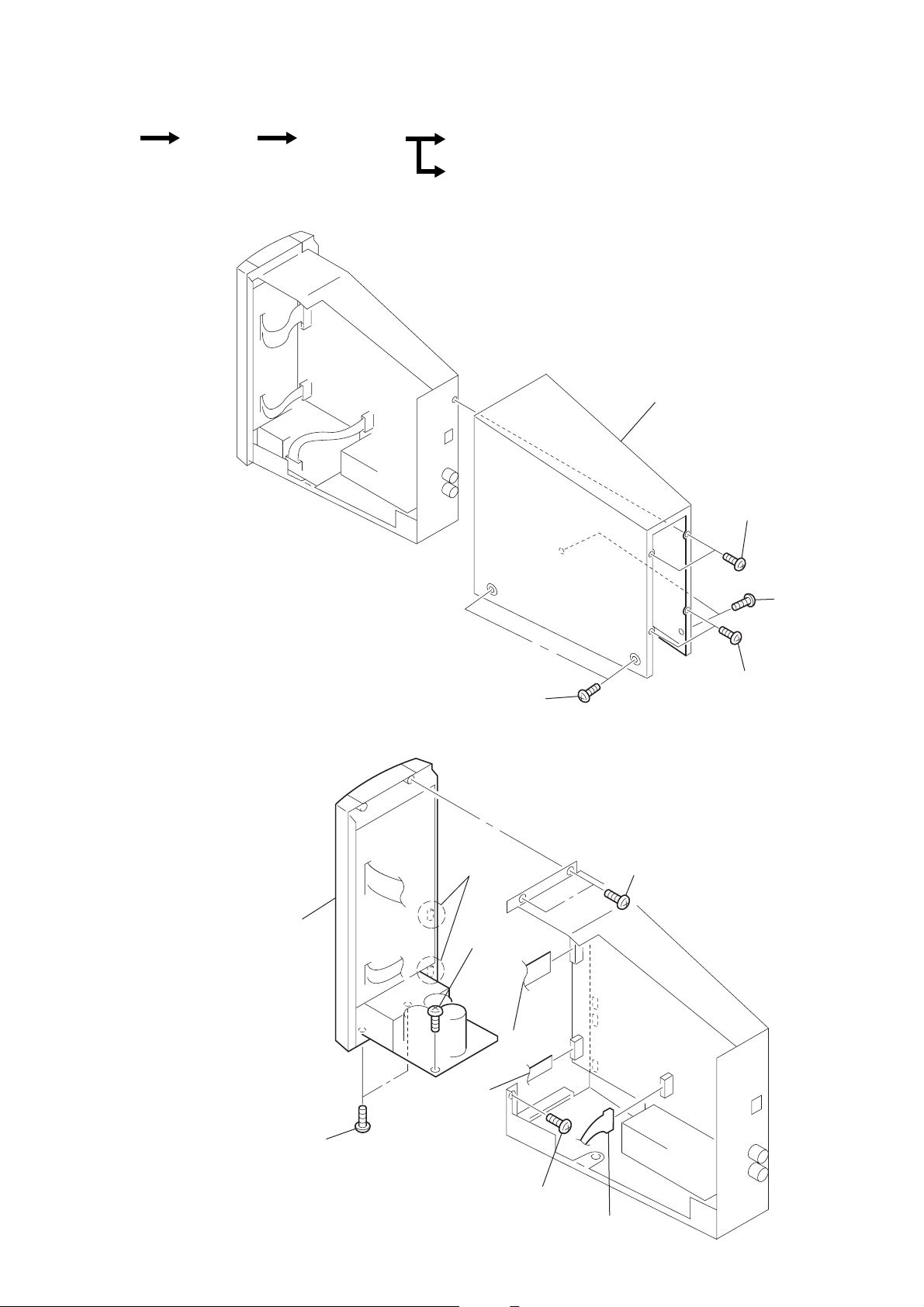
2-1. Cover Assy ..........................................................................5
2-2. Panel Assy, Front................................................................. 5
2-3. Panel Assy, Sub ................................................................... 6
2-4. TX Board ............................................................................ 6
3. SERVICE MODE
3-1. General ................................................................................ 7
3-2. Setting the Test Mode.......................................................... 7
3-3. Releasing the Test Mode ..................................................... 7
3-4. Test Mode............................................................................ 7
4. ELECTRICAL ADJUSTMENTS................................... 8
5. DIAGRAMS
5-1. IC Pin Descriptions ............................................................. 9
5-1-1. IC201 µPD784216 (Program, System Control) ............ 9
5-1-2. IC301 CXD9511AQ (Dolby Digital (AC-3)/
Pro Logic, DTS Decoder)............................................ 11
5-1-3. IC302 XCB56362PV100 (24 Bit Audio Digital
Signal Processor) .........................................................13
5-2. Block Diagrams ................................................................ 17
5-2-1. Block Diagram –Processor Section– ........................... 17
5-2-2. Block Diagram –Transmitter Section–........................ 19
5-3. Printed Wiring Boards and Schematic Diagrams..............21
5-3-1. Printed Wiring Board –TX Board– ............................. 21
5-3-2. Schematic Diagram –TX Board (1/2)– ....................... 25
5-3-3. Schematic Diagram –TX Board (2/2)– ....................... 27
5-3-4. Printed Wiring Board –LED Board–........................... 29
5-3-5. Schematic Diagram –LED Board–.............................. 31
5-3-6. Printed Wiring Board –AMP Board– .......................... 33
5-3-7. Schematic Diagram –AMP Board– ............................. 34
5-4. IC Block Diagrams ........................................................... 35
6. EXPLODED VIEW........................................................... 38
7. ELECTRICAL PARTS LIST......................................... 39
– 2 –
SECTION 1
GENERAL
This section is extracted
from instruction manual.
– 3 –
– 4 –
SECTION 2
3
PTT 2.6X5
5
cover assy
2
PTT 2.6X5
4
PTT 2.6X5
1
PTT 2.6X5
DISASSEMBLY
• The equipment can be removed using the following procedure.
Set Cover assy Panel assy, front Panel assy, sub
TX board
Note : Follow the disassembly procedure in the numerical order given.
2-1. COVER ASSY
2-2. PANEL ASSY, FRONT
9
panel assy, front
1
screws (2.6x6)
4
CN103
8
claws
2
PTT 2.6X5
3
CN102
7
P 3X6
5
CN101
6
P 3X6
– 5 –
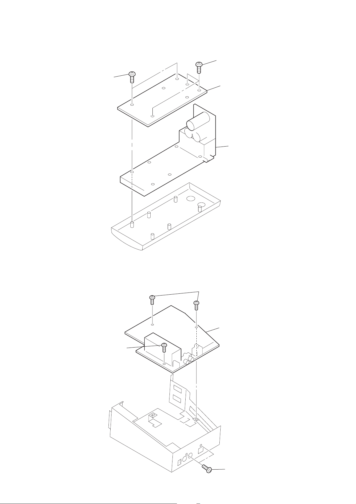
2-3. PANEL ASSY, SUB
b
2
P 2X8
1
P 2X8
3
LED board
4
panel assy, su
2-4. TX BOARD
3
screw BTT
2
screws BTT
4
TX board
– 6 –
1
BVTP 3X8
SECTION 3
SERVICE MODE
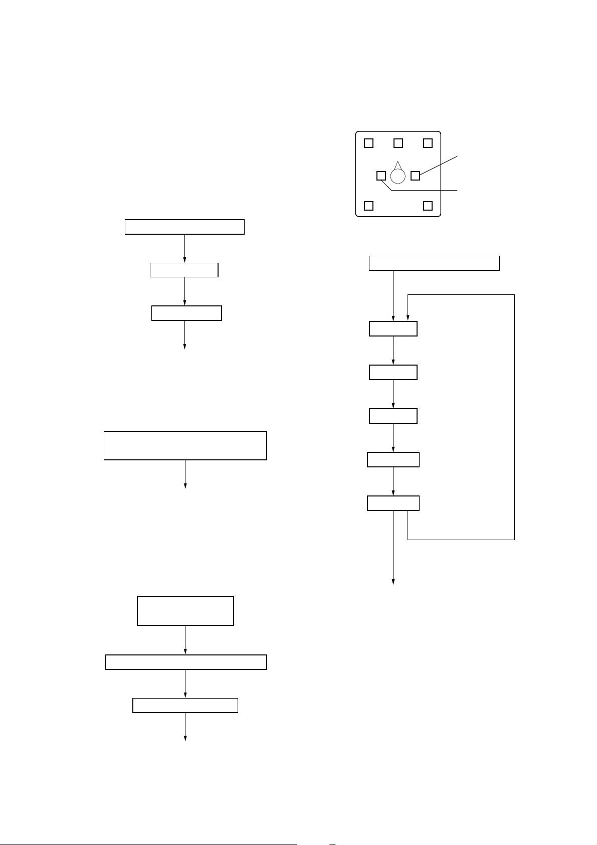
3-1. GENERAL
This set has the test mode of the built-in microprocessor which
allows various check items required repairing.
3-2. SETTING THE TEST MODE
Press the POWER key and the EFFECT key at the same time and
turn on the power. (Insert the DC plug)
3-3. RELEASING THE TEST MODE
Remove the DC plug.
3-4. TEST MODE
1. LED check
LEDs go on in sequence *1)
POWER,INPUT keys
All LEDs on
All LEDs off
Go to Key check
*2)
POWER,INPUT keys
*3)
*5) Digital input check : Do not use this in repair.
*6) Analog input check :Other than MUTE check, do not use this
in repair.
*7) Mute mode : Use this in electrical adjustment (see page 8).
*8)
C
L
LS
4. IF test tone
POWER and MUSIC LEDs on
L LED on
R
RS
OUTPUT key
1 kHz, –10 dBv
OUTPUT key
HR LED
HL LED
*1) In test mode
*2) All infrared LEDs on
*3) All infrared LEDs on
2. Key check
Press each key and its corresponding
LED goes on *4)
Go to Audio check
*4) Corresponding LEDs
POWER key : POWER LED
INPUT key : ANALOG LED
EFFECT key : MUSIC LED
OUTPUT key : VIRTUAL LED
3. Audio check
POWER, DIGITAL,
L and R LEDs on *5)
ANALOG, HR and HL LEDs on *5) *7)
POWER,INPUT keys
POWER,INPUT keys
C LED on
OUTPUT key
R LED on
OUTPUT key
RS LED on
OUTPUT key
LS LED on
OUTPUT key
POWER,INPUT keys
End of Test mode
1 kHz, –30 dBv
100 Hz, –30 dBv
10 kHz, –30 dBv
1 kHz, FS
POWER,INPUT keys
HL and HR LEDs off *6)
POWER,INPUT keys
Go to IF test tone
– 7 –
SECTION 4
ELECTRICAL ADJUSTMENTS
Notes:
1. These adjustments are performed in the order that they are
described.
2. Adjustment and measurement are performed for each channel
unless otherwise specified.
3. Adjustment is made for the right channel first and then the left
channel.
4. The power voltage is supplied with 9 V.
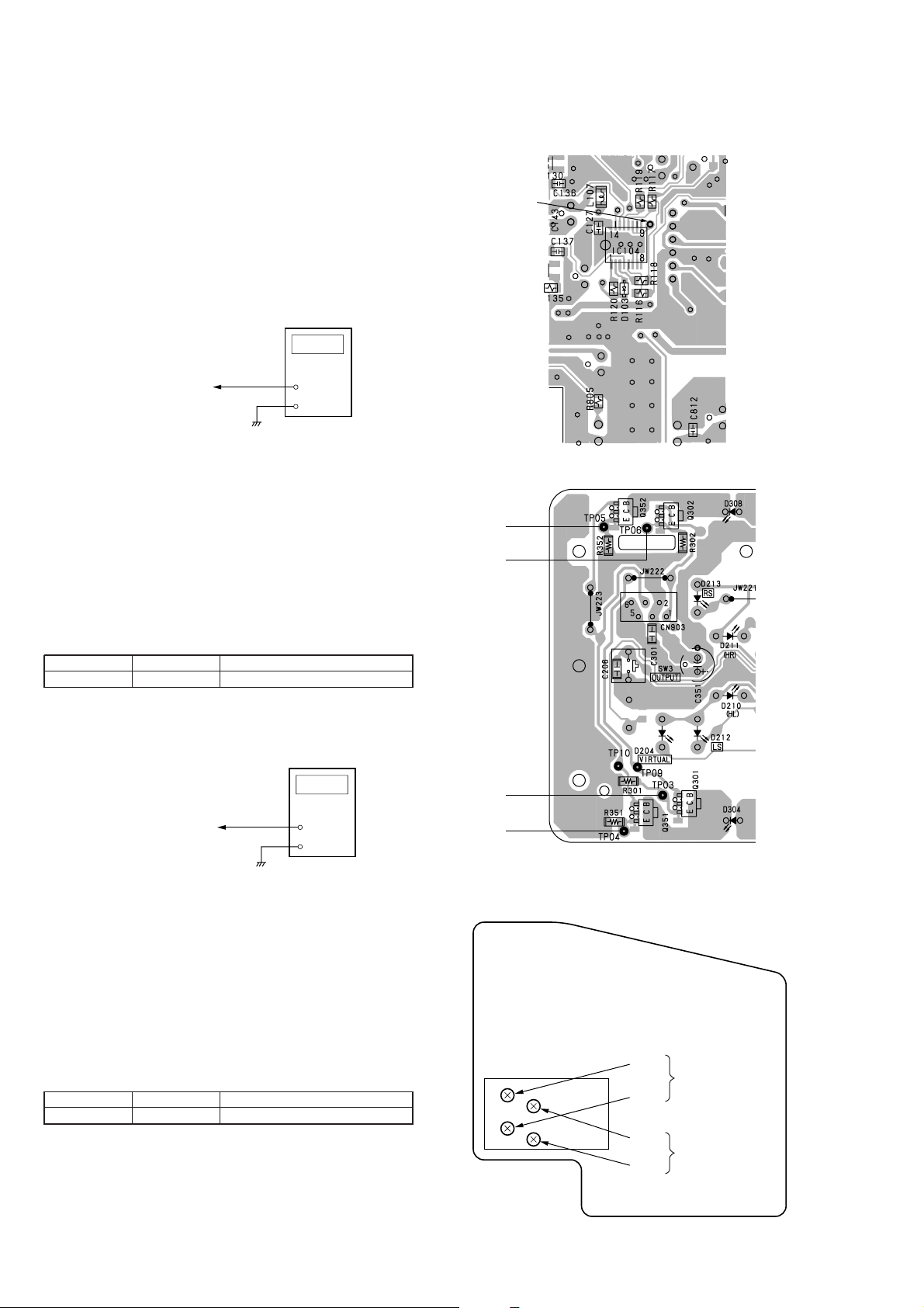
Oscillation Frequency Adjustment
Setting:
digital frequency
counter
TP03 or TP04 (L-ch)
TP05 or TP06 (R-ch)
LED board
+
–
Adjustment method:
• Perform this adjustment without signal.
1. Connect TP (A MUTE) to ground on the TX board (to set the
mute state), or use the test mode to set the mute state (see page
7).
2. Connect a digital frequency counter to TP03 or TP04 for L-ch
and TP05 or TP06 for R-ch on the LED board.
3. Adjust L51 (L-ch) and L1 (R-ch) on the TX board so that the
reading on the digital frequency counter is each within 2.3 MHz
(L-ch) and 2.8 MHz (R-ch).
Adjustment Location:
– TX board (side A) –
TP
(A MUTE)
– LED board (conductor side) –
TP05
TP06
Specified value:
L-ch L51 2.298 to 2.302 MHz
R-ch L1 2.798 to 2.802 MHz
RF Level Adjustment
Setting:
digital voltmeter
TP03 or TP04 (L-ch)
TP05 or TP06 (R-ch)
LED board
+
–
Adjustment method:
• Perform this adjustment without signal.
1. Connect TP L (L-ch) and TP R (R-ch) to ground on the LED
board (to set the mute state), or use the test mode to set the mute
state (see page 7).
2. Connect a digital voltmeter to TP03 or TP04 for L-ch and TP05
or TP06 for R-ch on the LED board.
3. Adjust RV51 (L-ch) and RV1 (R-ch) on the TX board so that
the reading on the digital voltmeter is 480 mV.
Specified value:
L-ch RV51 477.5 to 482.5 mV
R-ch RV1 477.5 to 482.5 mV
TP03
TP04
– TX board (side A) –
RV51
RV1
L51
L1
RF LEVEL
ADJUSTMENT
OSCILLATION
FREQUENCY
ADJUSTMENT
– 8 –
SECTION 5
DIAGRAMS
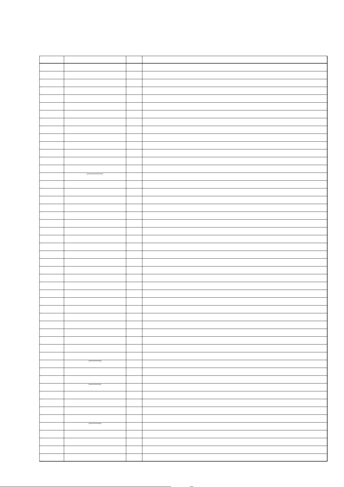
5-1. IC PIN DESCRIPTIONS
5-1-1. IC201 µPD784216 (PROGRAM, SYSTEM CONTROL)
Pin No. Pin Name I/O Pin Description
1 RTP0/P120 O Analog circuit block mute signal output (H: Mute)
2 RTP1/P121 O D/A mute signal output (H: Mute)
3 RTP2/P122 O IF circuit block power control signal output (H: ON)
4 RTP3/P123 O Main circuit block power control signal output (H: ON)
5 RTP4/P124 O DIR block clock select signal output (H: Digital, L: Analog)
6 RTP5/P125 O DIR serial select signal output
7 RTP6/P126 — Not used. (Open)
8 RTP7/P127 — Not used. (Open)
9 VDD I Power supply pin
10 X2 O Connect to crystal for main system clock oscillator
11 X1 I Connect to crystal for main system clock oscillator
12 VSS — Ground
13 XT2 — Not used. (Open)
14 XT1 — Not used. (Fix to “L”.)
15 RESET I Reset signal input
16 INTP0/P00 I DIR audio data detect signal input
17 INTP1/P01 — Not used. (Open)
18 INTP2/P02 O Sub DSP serial select signal output
19 INTP3/P03 O Decoder serial select signal output
20 INTP4/P04 O Main DSP serial select signal output
21 INTP5/P05 O SLAVE reset signal output
22 INTP6/P06 I DIR lock signal input
23 AVDD I Power supply pin
24 AVREF0 — Ground
25 ANI0/P10 I DSP serial BUSY 5 V signal input
26 ANI1/P11 — Not used. (Open)
27 ANI2/P12 I Not used. (Open)
28 ANI3/P13 I Not used. (Open)
29 ANI4/P14 I Not used. (Open)
30 ANI5/P15 I Auto mute detect signal (L: OFF, H: ON)
31 ANI6/P16 — Not used. (Open)
32 ANI7/P17 I Audio input level signal input
33 AVSS — Analog ground
34 ANO0/P130 — Not used. (Open)
35 ANO1/P131 — Not used. (Open)
36 AVREF1 I Power supply pin
37 SI2 I Main serial data signal input
38 SO2 O Main serial data signal output
39 SCK2 O Main serial clock signal output
40 SI1 I Main serial data signal input
41 SO2 O Not used. (Open)
42 SCK1 O Main serial clock signal output
43 PCL/P23 O Main DSP reset signal output
44 BUZ/P24 — Not used.
45 SI0 I LED/FLASH serial data signal input
46 SO0 O LED/FLASH serial data signal output
47 SCK0 O LED/FLASH serial clock signal output
48 A0/P80 O Main DSP mute signal output
49 A1/P81 O Not used. (Main DSP ATT setting bit HIGH)
50 A2/P82 O Not used. (Main DSP ATT setting bit LOW)
51 A3/P83 O Main DSP ALC ON signal output
– 9 –
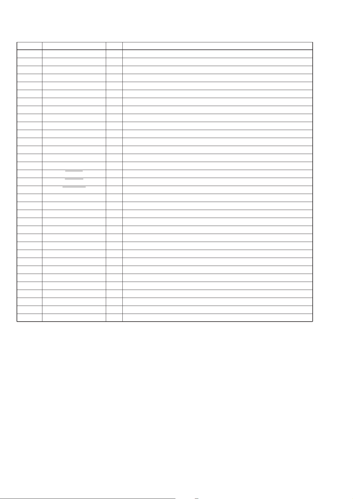
Pin No. Pin Name I/O Pin Description
52 A4/P84 O Main DSP VR setting bit HIGH signal output
53 A5/P85 O Main DSP VR setting bit LOW signal output
54 A6/P86 O Reserve terminal (Fix to “L”.)
55 A7/P87 O Reserve terminal (Fix to “L”.)
56 – 63 AD0 – 7/P40 – 47 — Not used. (Open)
64 A8/P50 O Not used. (Open) (LED 0)
65 A9/P51 O Not used. (Open) (LED 1)
66 A10/P52 O Not used. (Open) (LED 2)
67 A11/P53 O Not used. (Open) (LED 3)
68 – 71 A12 – 15/P54 – 57 — Not used. (Open)
72 VSS — Ground
73 A16/P60 I Power on/off key input
74 A17/P61 I INPUT key input
75 A18/P62 I EFFECT key input
76 A19/P63 I OUTPUT key input
77 RD/P64 I Jump key input
78 WR/P65 I Not used. (Open)
79 WAIT/P66 I Not used. (Open)
80 ASTB/P67 I Not used. (Open)
81 VDD I Power supply pin
82 T05/P100 O LEDEN signal output
83 T06/P101 O LEDLAT signal output
84 T07/P102 O LEDRESET signal output
85 T08/P103 — Not used. (Open)
86 T00/P30 — Not used. (Open)
87 T01/P31 — Not used. (Open)
88 T02/P32 — Not used. (Open)
89 T03/P33 — Not used. (Open)
90 T04/P34 — Not used. (Open)
91 TI00/P35 — Not used. (Open)
92 TI01/P36 — Not used. (Open)
93 P37 — Not used. (Open)
94 VPP I VPP signal input
95 – 100 P90 – 95 — Not used. (Open)
– 10 –
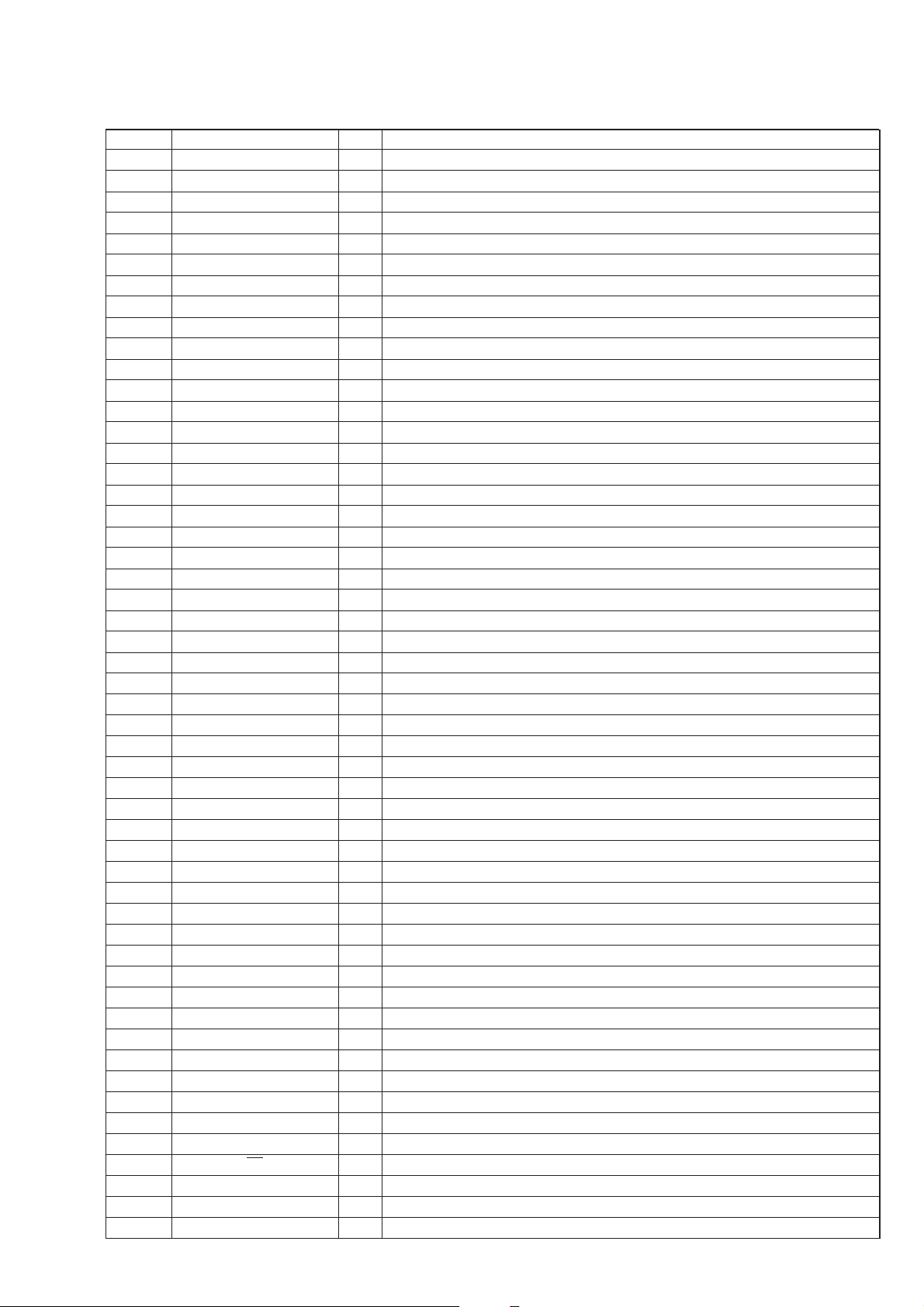
5-1-2. IC301 CXD9511AQ (DOLBY DIGITAL (AC-3)/PRO LOGIC, DTS DECODER)
Pin No. Pin Name I/O Pin Description
1 VDD1 I Power supply pin (+5 V)
2 RAMCEN — Not used. (Open)
3 • 4 RAM16 • 15 — Not used. (Open)
5 SDIB0 I PCM signal input
6 • 7 SDIB1 • 2 — Not used. (Open)
8 XI I External system clock signal input (12.288 MHz)
9 XO — Not used. (Open)
10 VSS — Ground
11 AVDD I Power supply pin (+3.3 V)
12 SDIB3 — Not used. (Open)
13 • 14 TEST — Test pin
15 OVFB — Not used. (Open)
16 DTSDATA — Not used. (Open)
17 AC3DATA — Not used. (Open)
18 SPDOB3 — Not used. (Open)
19 CPO O PLL signal output
20 AVSS — Ground
21 ADD2 I Power supply pin
22 SDOA2 O PCM signal output (C, LFE output)
23 SDOA1 O PCM signal output (LS, RS output)
24 SDOA0 O PCM signal output (L, R output)
25 – 29 RAMA14 – 10 — Not used. (Open)
30 VSS — Ground
31 VDD1 I Power supply pin (+5 V)
32 – 39 OPORT0 – 7 — Not used. (Open)
40 VSS — Ground
41 VDD2 I Power supply pin (+3.3 V)
42 – 44 RAMA9 – 7 — Not used. (Open)
45 SDOB2 — Not used. (Open)
46 SDOB1 O PCM signal output
47 SDOB0 O PCM signal output
48 SDBCK1 — Not used. (Open)
49 SDWCK1 — Not used. (Open)
50 VSS — Ground
51 VDD2 I Power supply pin (+3.3 V)
52 NONPCM — Not used. (Open)
53 CRC — Not used. (Open)
54 MUTE O Auto mute detect signal output
55 KARAOKE — Not used. (Open)
56 SCRENC — Not used. (Open)
57 SDBCK0 O SDBCK0 turn over clock signal output
58 • 59 RAMA6 • 5 — Not used. (Open)
60 VSS — Ground
61 RAMA4 — Not used. (Open)
62 IC I Initial clear terminal
63 TEST — Test pin
64 RAMA3 — Not used. (Open)
65 CSB I Sub DSP chip select signal input
66 CS I Interface chip select signal input
67 SO O Interface data signal output
68 SI I Interface and sub DSP data signal input
69 SCK I Interface and sub DSP clock signal input
– 11 –
 Loading...