

Page 1

DP-IF5000
SERVICE MANUAL
Ver 1.1 1999. 02
Manufactured under license from Dolby Laboratories Licensing
•
Corporation.
DOLBY, the double-D symbol a , “PRO LOGIC”,
“Dolby Digital (AC-3)”, and “VIRTUAL DOLBY DIGITAL” are
trademarks of Dolby Laboratories Licensing Corporation.
DP-IF5000 is the component model block one in
•
MDR-DS5000.
COMPONENT MODEL NAME FOR MDR-DS5000
DIGITAL SURROUND PROCESSOR DP-IF5000
CORDLESS STEREO HEADPHONES MDR-IF5000
US Model
Canadian Model
AEP Model
UK Model
E Model
SPECIFICATIONS
Modulation System Frequency modulation
Carrier wave frequency Right channel 2.8 MHz
Left channel 2.3 MHz
Transmission distance Approx. 10 m
Frequency response 20 – 20,000 Hz
Distortion rate 1% or less (1 kHz)
Audio inputs Optical input
(square-type) × 1
Analog input (pin jack
right/left) × 1
Power requirements DC 9 V (from the
supplied AC power
adapter)
Dimensions (w/h/d) Approx. 85 × 190 × 180
mm
Mass Approx. 1.0 kg
(1000 g)
MICROFILM
Design and specifications are subject to
change without notice.
Notes on Chip Component Replacement
• Never reuse a disconnected chip component.
• Notice that the minus side of a tantalum capacitor may be dam-
aged by heat.
DIGITAL SURROUND PROCESSOR
– 1 –
Page 2

TABLE OF CONTENTS
1. GENERAL
Listening to the Sound of a Connected Component ............... 3
2. DISASSEMBLY
2-1. Cover Assy .......................................................................... 5
2-2. Panel Assy , Front.................................................................5
2-3. Panel Assy , Sub ................................................................... 6
2-4. TX Board ............................................................................ 6
3. SERVICE MODE
3-1. General ................................................................................ 7
3-2. Setting the Test Mode.......................................................... 7
3-3. Releasing the Test Mode ..................................................... 7
3-4. Test Mode............................................................................7
4. ELECTRICAL ADJUSTMENTS...................................8
5. DIAGRAMS
5-1. Block Diagram –Processor Section–................................... 9
5-2. Block Diagram –Transmitter Section–..............................11
5-3. Printed Wiring Board
–Processor, Transmitter Section–...................................... 14
5-4. Schematic Diagram –Processor Section– ......................... 17
5-5. Schematic Diagram –Transmitter Section– ......................20
5-6. Printed Wiring Board –LED Section– .............................. 22
5-7. Schematic Diagram –LED Section– .................................23
5-8. Printed Wiring Board –Amplifier Section–....................... 25
5-9. Schematic Diagram –Amplifier Section– .........................26
5-10. IC Pin Descriptions........................................................... 29
6. EXPLODED VIEW........................................................... 34
7. ELECTRICAL PARTS LIST......................................... 35
– 2 –
Page 3
SECTION 1
GENERAL
This section is extracted
from instruction manual.
– 3 –
Page 4
– 4 –
Page 5
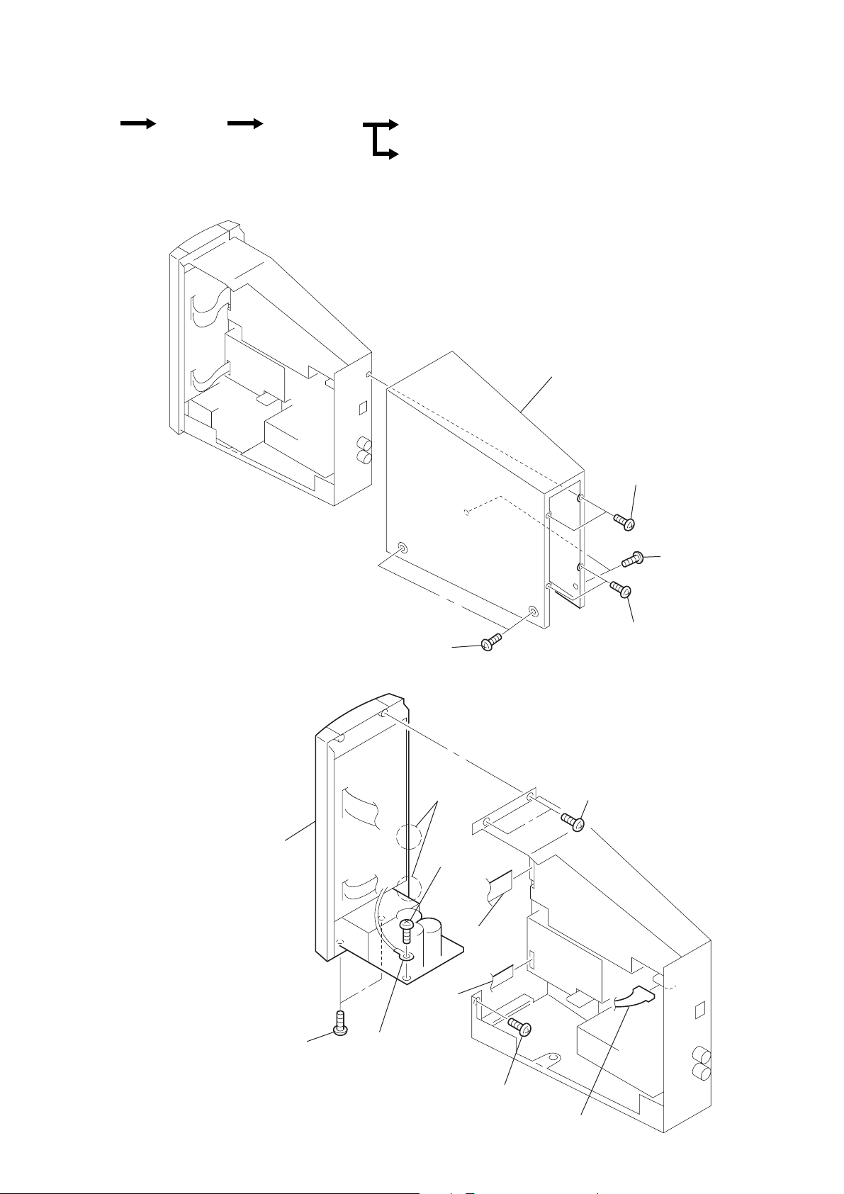
SECTION 2
5
DISASSEMBLY
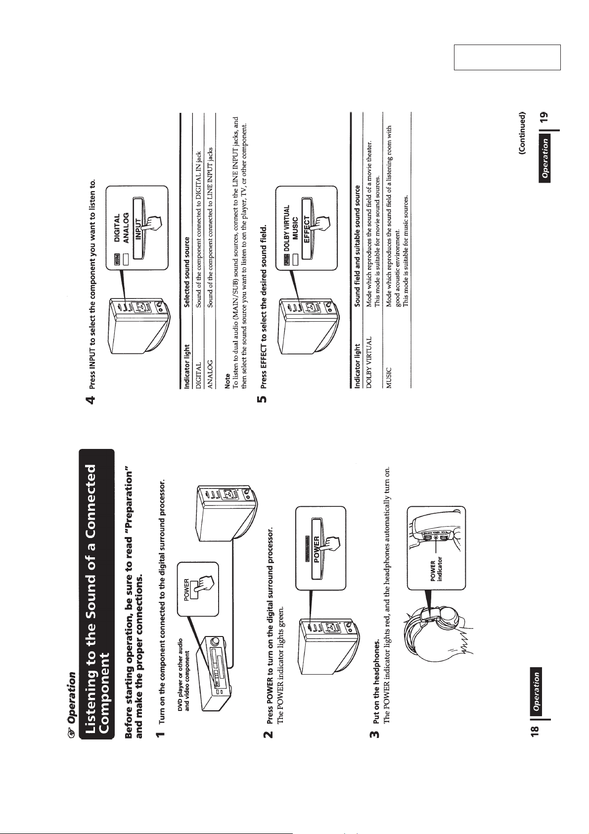
• The equipment can be removed using the following procedure.
Set Cover assy Panel assy, front Panel assy, sub
TX board
Note : Follow the disassembly procedure in the numerical order given.
2-1. COVER ASSY
5
cover assy
2-2. PANEL ASSY, FRONT
!º
panel assy, front
1
PTT 2.6X5
9
claws
2
PTT 2.6X5
7
P 3X6
3
PTT 2.6X5
2
4
PTT 2.6X5
PTT 2.6X
1
PTT 2.6X5
3
lug plate
5
CN103
– 5 –
4
CN102
8
P 3X6
6
CN901
Page 6
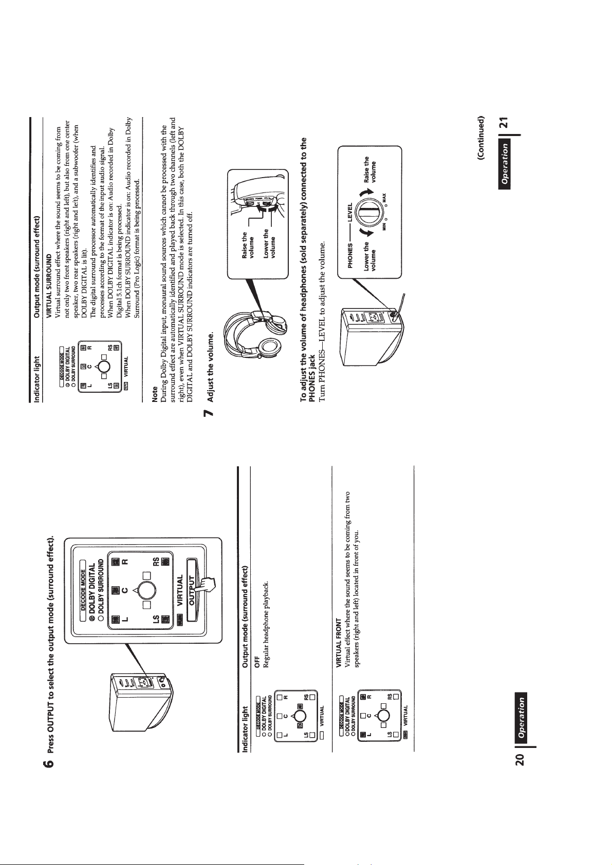
2-3. PANEL ASSY, SUB
b
2
P 2.6X6
1
P 2.6X6
3
LED board
4
panel assy, su
2-4. TX BOARD
3
PTT 2.6X5
2
PTT 2.6X5
4
TX board
– 6 –
1
P 3X6
Page 7
SECTION 3
SERVICE MODE
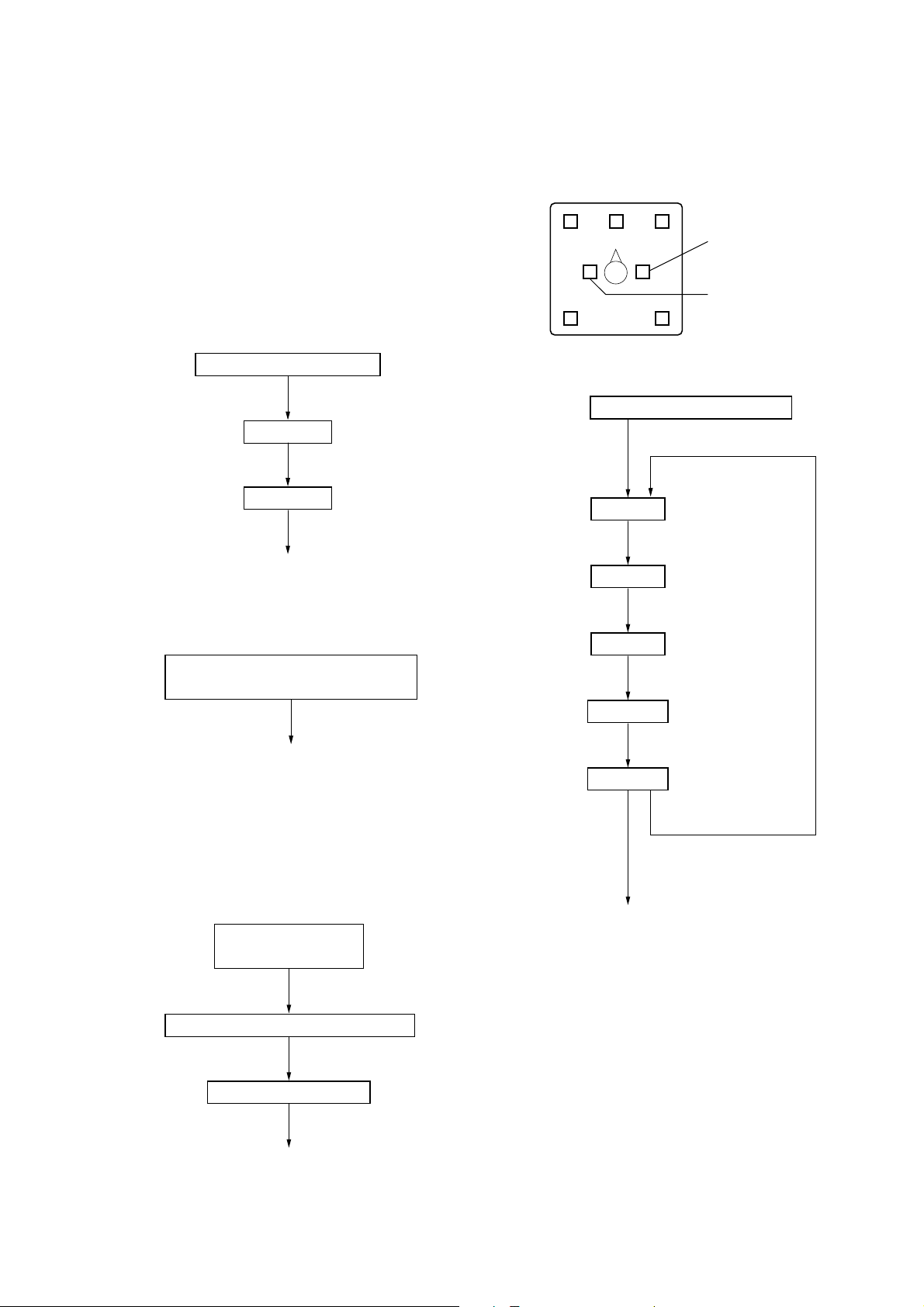
3-1. GENERAL
This set has the test mode of the built-in microprocessor which
allows various check items required repairing.
3-2. SETTING THE TEST MODE
Press the POWER key and the EFFECT key at the same time and
turn on the power. (Insert the DC plug.)
3-3. RELEASING THE TEST MODE
Press the POWER key to turn of f the power . (Remove the DC plug.)
3-4. TEST MODE
1. LED check
LEDs go on in sequence *1)
DEMO key
All LEDs on
DEMO key
All LEDs off
Go to Key check
*1) In test mode
2. Key check
Press each key and its corresponding
LED goes on *2)
DEMO key
Go to Audio check
*2) Corresponding LEDs
POWER key : POWER LED
INPUT key : ANALOG LED
EFFECT key : MUSIC LED
OUTPUT key : VIRTUAL LED
*3) Digital input check : Do not use this in repair.
*4) Analog input check :Other than MUTE check, do not use this
in repair.
*5) Mute mode : Use this in electrical adjustment (see page 8).
*6)
C
L
LS
4. IF test tone
POWER and MUSIC LEDs on
L LED on
C LED on
R LED on
RS LED on
LS LED on
R
RS
OUTPUT key
1 kHz, –10 dBv
OUTPUT key
1 kHz, –30 dBv
OUTPUT key
100 Hz, –30 dBv
OUTPUT key
10 kHz, –30 dBv
OUTPUT key
1 kHz, FS
OUTPUT key
DEMO key
HR LED
HL LED
3. Audio check
ANALOG, HR and HL LEDs on *4) *6)
End of Test mode
POWER, DIGITAL,
L and R LEDs on *3)
DEMO key
DEMO key
HL and HR LEDs off *5)
DEMO key
Go to IF test tone
– 7 –
Page 8
SECTION 4
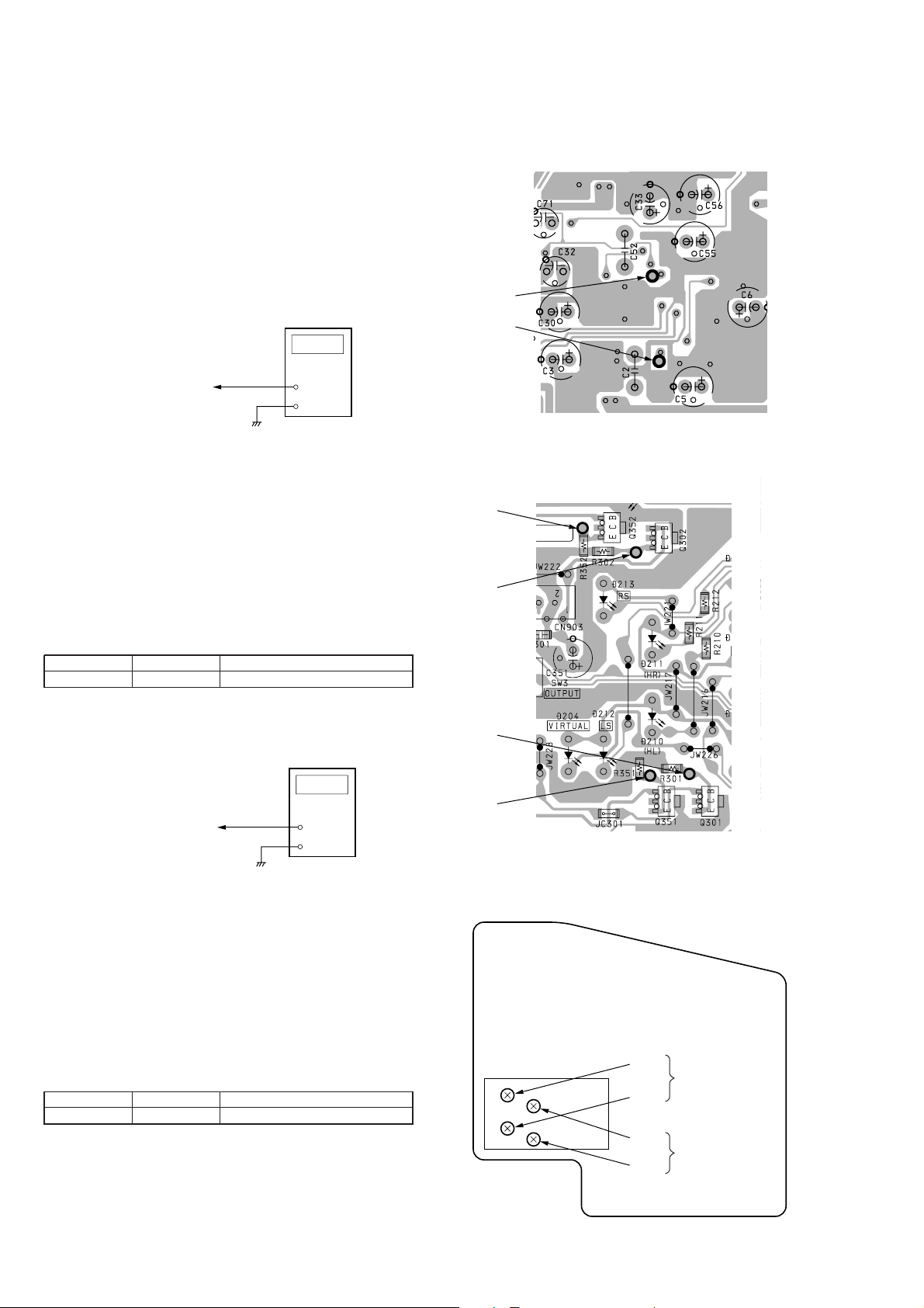
ELECTRICAL ADJUSTMENTS
Notes:
1. These adjustments are performed in the order that they are
described.
2. Adjustment and measurement are performed for each channel
unless otherwise specified.
3. Adjustment is made for the right channel first and then the left
channel.
4. The power voltage is supplied with 9 V.
Oscillation Frequency Adjustment
Setting:
digital frequency
counter
TP03 or TP04 (L-ch)
TP05 or TP06 (R-ch)
LED board
+
–
Adjustment method:
• Perform this adjustment without signal.
1. Connect TP L (L-ch) and TP R (R-ch) to ground on the LED
board (to set the mute state), or use the test mode to set the mute
state (see page 7).
2. Connect a digital frequency counter to TP03 or TP04 for L-ch
and TP05 or TP06 for R-ch on the LED board.
3. Adjust L51 (L-ch) and L1 (R-ch) on the TX board so that the
reading on the digital frequency counter is each within 2.3 MHz
(L-ch) and 2.8 MHz (R-ch).
Adjustment Location:
– TX board (side B) –
TP L
TP R
– LED board (conductor side) –
TP05
TP06
TP L
TP R
TP05
TP06
Specified value:
L-ch L51 2.298 to 2.302 MHz
R-ch L1 2.798 to 2.802 MHz
RF Level Adjustment
Setting:
digital voltmeter
TP03 or TP04 (L-ch)
TP05 or TP06 (R-ch)
LED board
+
–
Adjustment method:
• Perform this adjustment without signal.
1. Connect TP L (L-ch) and TP R (R-ch) to ground on the LED
board (to set the mute state), or use the test mode to set the mute
state (see page 7).
2. Connect a digital voltmeter to TP03 or TP04 for L-ch and TP05
or TP06 for R-ch on the LED board.
3. Adjust RV51 (L-ch) and RV1 (R-ch) on the TX board so that
the reading on the digital voltmeter is 480 mV.
Specified value:
L-ch RV51 477.5 to 482.5 mV
R-ch RV1 477.5 to 482.5 mV
TP03
TP04
– TX board (side A) –
TP04
RV51
RV1
L51
L1
TP03
RF LEVEL
ADJUSTMENT
OSCILLATION
FREQUENCY
ADJUSTMENT
– 8 –
Page 9
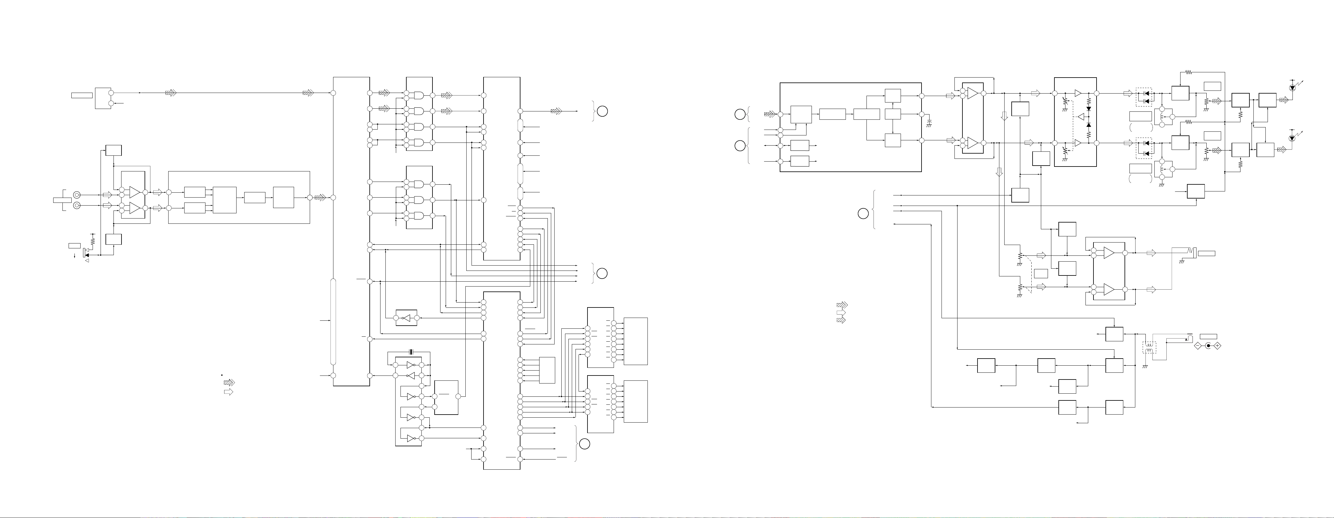
SECTION 5
DIAGRAMS
DP-IF5000
5-1. BLOCK DIAGRAM — PROCESSOR SECTION —
OPTICAL
RECEIVER
MODULE
IC305
DIGITAL
1
B+
(+9V)
OUT
VCC
3
ATT SW
Q101
ATT SW
Q102
(+5V)
2
3
5
6
B+
LINE AMP
IC101
–
+
–
+
V IN L
1
6
1
6
V IN R
FRONT END
FRONT END
J101
LINE INPUT
–1
L
R
–2
SW101
–6dB
DIGITAL IN
ANALOG L
ANALOG R
ATT
0dB
ANALOG
ANALOG
+
–
+
–
A/D CONVERTER
DELTA
SIGMA
MODULATOR
Signal path
IC102 (1/2)
DECIMATION
: DIGITAL
: ANALOG
FILTER
DIGITAL
AUDIO
INTERFACE
(1/2)
D OUT
19
(+3.3V)
(+3.3V)
DIGITAL
B+
B+
AC-3/PROLOGIC
SURROUND DECODER
IC301
61 80
SPFRK
8319
SDA
6
•
12
•
17
•
30
•
35
•
45
VDD
•
55
•
59
•
67
•
81
•
84
•
93
70
VCCA
SDB
SBC
SCKB
SCKA
WSB
WSA
SCKIN
SO
GPIO0
SI
SCK
RESET
SS
XT1
79
95
91
95
92
66
34
58
SO1
89
SCK1
87
82
3
CLOCK 12M
64
FRONT LR
REAR LR
BCK 64fs
L/R 1fs
MCK 256fs
9
10
12
13
5
4
1
2
B+
(+5V)
5
4
2
1
13
12
B+
(+5V)
INVERTER
IC203(1/2)
12 13
X201
12.288MHz
1 2
6
INVERTER
IC203(2/2)
NAND
IC303
8
11
6
3
NAND
IC304
6
3
11
5
CMOS LOGIC
3
4
11
10
8 41
IC201
10 6
CLOCKQ1Q3
9
B+
(+5V)
PROCESSOR
57
SDI0
56 47
SDI1
51
SCKR
49
SCKT
55
WSR
50
WST
35
MISO/SDA
41
SI
26
SCK/SCL
SI1
57
P20(SI1)
37
P01
S01
58
P21(SO1)
SCK1
59
P22(SCK1)
RESET
49
SSZ11
X1
X2
P12
48
P11
PROGRAM,
SYSTEM
CONTROL
42
X1
X2
40
V
55
AV
IC105
DD
LOGIC 3D
IC302
P24(BUSY)
DD
SDO0
VCCA
VCCD
VCCP
VCCQ
VCCS
HREQ
RESET
GPIO3
GPIO2
GPIO1
GPIO0
EXTAL
P64
P65
P66
P67
P17
P10
P40
P41
P42
P43
P44
P50
P51
P52
P27
P26
P16
P15
P57
RESET
5-2. BLOCK DIAGRAM — TRANSMITTER SECTION —
B+
(+9V)
B+
(+9V)
INFRARED
EMITTER
D301-304
INFRARED
EMITTER
D305-308
REG
Q35, 36
RF LEVEL
(L-CH)
RF LEVEL
(R-CH)
J901
PHONES
J801
DC IN 9V
RV51
RV1
BUFFER
Q52
BUFFER
Q2
LED
DRIVE
Q301,351
LED
DRIVE
Q302,352
AFC
MUTE
Q901
MUTE
Q902
SW+9V
REG
Q803
RESET
IC204
(+5V)
IC1
B+
B+
(+9V)
6
5
3
2
BINAURAL L
7
BINAURAL R
1
–
+
HEADPHONES
AMP
IC901
+
–
+9V
REG
IC805
+9V
REG
IC804
+5V
REG
IC801
D/A CONVERTER
LR DATA
6
•
17
70
30
9
•
28
•
53
40
•
48
43
42
CS
36
73
74
75
76
27
31
32
33
34
54
47
61
10
11
12
13
14
18
19
20
64
63
539
52
26
35
BUSY
RESET
POWER
SELECT
MODE
EFFECT
DEMO
LEDEN
LEDLAT
LEDRES
SCK0
SO0
B+
(+5V)
B+
(+5V)
B+
(+5V)
B+
(+5V)
B+
(+5V)
BLOCK
SW1-5
SW
MUTE
POWER A
POWER B
RESET
LRCK
BCKIN
CLK10
RST
3
EN
2
LATO2O3
3
RES
15
SCK
14
SIN
13
SO
4
SIN O2
13
EN
2
LAT
3
RES
15
SCK
14
TRANSMITTER
1
SECTION
TRANSMITTER
2
SECTION
DISPLAY
LED DRIVE
IC205
O1
12
11
10
O4
9
O5
8
O6
7
O7
6
O8
5
O1
12
11
O3
10
O4
9
O5
8
O6
7
O8
5
DISPLAY
LED DRIVE
IC206
TRANSMITTER
SECTION
DISPLAY
LED DRIVE
D201-208
DISPLAY
LED
D209-214,216
PROCESSOR
SECTION
PROCESSOR
SECTION
LR DATA
1
LRCK
BCK IN
CLK10
2
RST
DIGITAL
DIN
AUDIO
18
INTERFACE
(
2/2
16
17
CLK/OSC
22
MANAGER
RESET
28
)
INTERPOLATION
FILTER
PROCESSOR
SECTION
• Signal path
: DIGITAL
: ANALOG
: RF
IC102 (2/2
)
DELTA SIGMA
MODULATION
3
MUTE
POWER A
POWER B
RESET
LPF
&
BUFFER
BIAS
LPF
&
BUFFER
V OUT L
V COM
V OUT R
BINAURAL L
15
11
+
BINAURAL R
12
B+
(+3.3V)
–
2
+
3
AUDIO AMP
IC103
+
5
–
6
1
7
+3.3V
REG
IC803
(SW+5V)
9
MUTE
Q31
13
MUTE
Q32
MUTING
SW
Q33,34
-1
L
RV901
PHONES
LEVEL
-2
R
+5V
REG
IC802
B+
B+
(SW+9V)
2.8MHz OSC
7
1
D51
L51
FREQUENCY
(L-CH)
2.3MHz OSC
COIL
D1
L1
FREQUENCY
(R-CH)
COIL
LF801
6
4
6
4
B+ (SW+5V)
OSC
Q51
2
OSC
Q1
2
SWITCH
– 9 – – 10 – – 11 –
– 12 –
Page 10
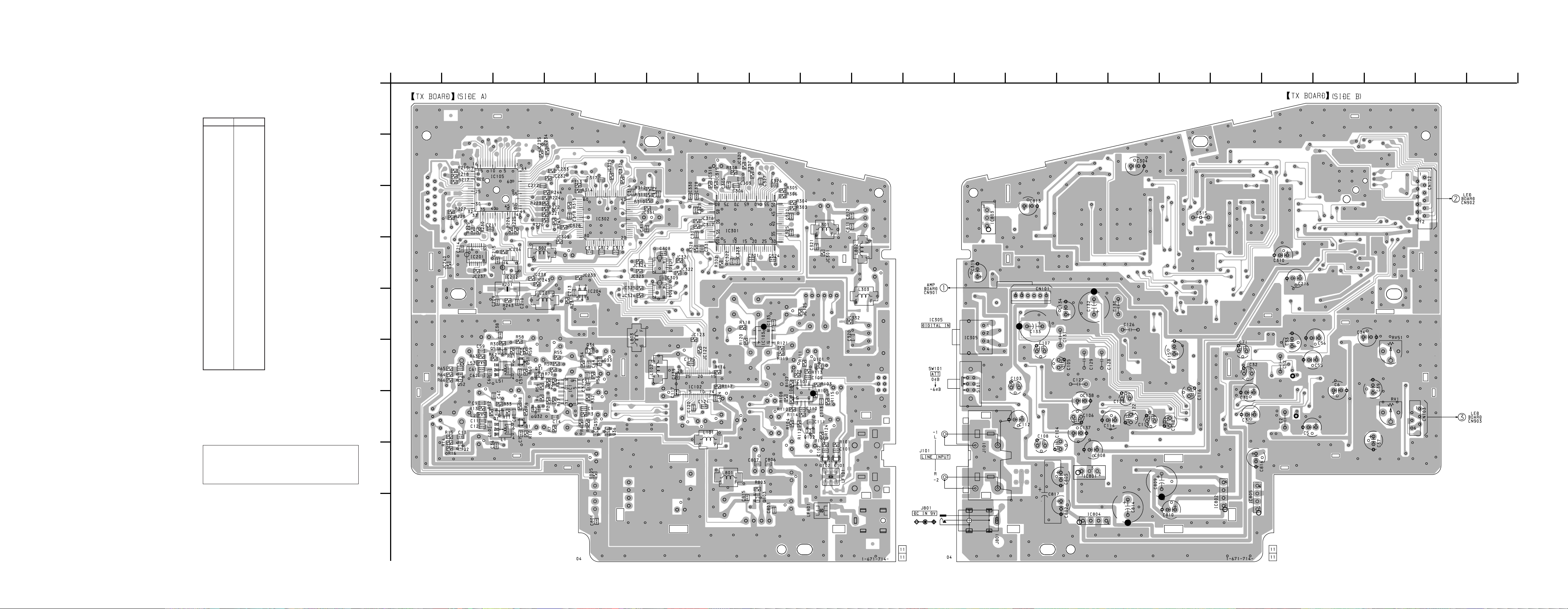
DP-IF5000
5-3. PRINTED WIRING BOARD — PROCESSOR, TRANSMITTER SECTION —
• Semiconductor
Location
Ref. No. Location
D1 G-3
D51 F-3
D101 H-9
D102 H-9
IC1 F-4
IC101 F-9
IC102 F-6
IC103 E-8
IC105 B-3
IC201 D-2
IC202 D-3
IC204 E-4
IC301 C-7
IC302 C-5
IC303 D-6
IC304 E-6
(IC305) C-12
(IC801) H-14
(IC802) I-7
(IC803) C-12
(IC804) I-14
(IC805) H-17
Q1 G-3
Q2 H-2
Q31 F-3
Q32 G-3
Q33 F-5
Q34 F-4
Q35 G-4
Q36 G-5
Q51 F-3
Q52 F-2
Q101 F-9
Q102 G-9
Q803 H-8
( ) : SIDE B
A
B
C
D
E
F
1
2345678910111213141516171819202122
(Page 22)
(Page 25)
TP L
Note:
• X : parts extracted from the component side.
®
•
• b : Pattern from the side which enables seeing.
Caution:
Pattern face side: Parts on the pattern face side seen from the
(Side B) pattern face are indicated.
Parts face side: Parts on the parts face side seen from the
(Side A) parts face are indicated.
: Through hole.
(The other layer’s patterns are not indicated.)
G
H
TP R
I
( )
– 13 – – 14 – – 15 – – 16 –
( )
(Page 22)
Page 11

5-4. SCHEMATIC DIAGRAM — PROCESSOR SECTION — • Refer to page 27 for IC Block Diagrams.
B
(Page 20)
(Page
26)
• Waveforms
1
IC102 !§ (LRCK)
2
IC102 !¶ (BCKIN)
3
12.288MHz
IC202
4
DP-IF5000
5Vp-p
80µsec
6.2Vp-p
1.3µsec
4.5Vp-p
2
4Vp-p
(Page 20)
(Page 23)
13µsec
IC301 (¡
(SCKA)
5
3.4Vp-p
80µsec
IC301 (™
(WSA)
6
6.2Vp-p
0.7µsec
IC302 @¶
Note:
• All capacitors are in µF unless otherwise noted. pF: µµF
50 WV or less are not indicated except for electrolytics
and tantalums.
• All resistors are in Ω and 1/
specified.
• C : panel designation.
• U : B+ Line.
• Total current is measured with Power ON/OFF mode.
• Power voltage is dc 9 V and fed with regulated dc power
supply from external power voltage jack.
• Voltage and waveforms are dc with respect to ground
under no-signal conditions.
no mark : POWER ON
• Voltages are taken with a VOM (Input impedance 10 MΩ).
Voltage variations may be noted due to normal production tolerances.
• Waveforms are taken with a oscilloscope.
Voltage variations may be noted due to normal production tolerances.
• Circled numbers refer to waveforms.
• Signal path.
F : ANALOG
c : DIGITAL
: Impossible to measure
∗
4
W or less unless otherwise
EXTAL
– 17 – – 18 – – 19 –
Page 12

DP-IF5000
5-5. SCHEMATIC DIAGRAM — TRANSMITTER SECTION — • Refer to page 27 for IC Block Diagrams.
B
(Page
17)
(Page 23)
5-6. PRINTED WIRING BOARD — LED SECTION —
1
23456
A
B
C
(Page 16)
D
D305-308
INFRARED
EMITTER
(R-CH)
D301-304
INFRARED
EMITTER
(L-CH)
Note:
• All capacitors are in µF unless otherwise noted. pF: µµF
50 WV or less are not indicated except for electrolytics
and tantalums.
• All resistors are in Ω and 1/
specified.
• U : B+ Line.
• H : adjustment for repair.
• Power voltage is dc 9 V and fed with regulated dc power
supply from external power voltage jack.
• Voltage is dc with respect to ground under no-signal
condition.
no mark : POWER ON
• Voltages are taken with a VOM (Input impedance 10 MΩ).
Voltage var iations may be noted due to normal production tolerances.
• Signal path.
F : ANALOG
J : RF
4
W or less unless otherwise
• Semiconductor
Location
Ref. No. Location
D201 A-4
D202 C-5
D203 C-5
D204 H-5
D205 F-5
D206 E-5
D207 F-5
D208 F-4
D209 F-3
D210 G-4
D211 G-3
D212 H-5
D213 H-3
D214 D-5
D216 D-5
D301 A-6
D302 C-6
D303 E-6
D304 G-6
D305 A-2
D306 C-2
D307 E-2
D308 G-2
E
F
G
H
TP03
TP06
TP05
(Page 16)
TP04
I
IC205 B-3
IC206 E-3
Q301 F-5
Q302 G-2
Q351 G-5
Q352 H-2
Note:
• X : parts extracted from the component side.
• b : Pattern from the side which enables seeing.
– 20 – – 21 – – 22 –
(Page 25)
Page 13

5-7. SCHEMATIC DIAGRAM — LED SECTION — • Refer to page 28 for IC Block Diagrams.
DP-IF5000
(Page 19)
(Page 21)
(Page 26)
Note:
• All capacitors are in µF unless otherwise noted. pF: µµF
50 WV or less are not indicated except for electrolytics
and tantalums.
• All resistors are in Ω and 1/
specified.
• C : panel designation.
• U : B+ Line.
• Power voltage is dc 9 V and fed with regulated dc power
supply from external power voltage jack.
• Voltage is dc with respect to ground under no-signal
condition.
no mark : POWER ON
• Voltages are taken with a VOM (Input impedance 10 MΩ).
Voltage var iations may be noted due to normal production tolerances.
• Signal path.
J : RF
: Impossible to measure
∗
4
W or less unless otherwise
– 23 – – 24 –
Page 14

DP-IF5000
5-8. PRINTED WIRING BOARD — AMPLIFIER SECTION —
1
23456
A
B
-2
-1
R
L
C
RV901
PHONES
LEVEL
D
5-9. SCHEMATIC DIAGRAM — AMPLIFIER SECTION —
(Page 15)
(Page 22)
(Page 23)
(Page 17)
E
• Semiconductor
Location
Ref. No. Location
IC901 D-4
Q901 B-2
Q902 B-2
Note:
• X : parts extracted from the component side.
• b : Pattern from the side which enables seeing.
Note:
• All capacitors are in µF unless otherwise noted. pF: µµF
50 WV or less are not indicated except for electrolytics
and tantalums.
• All resistors are in Ω and 1/
specified.
• C : panel designation.
• U : B+ Line.
• Power voltage is dc 9 V and fed with regulated dc power
supply from external power voltage jack.
• Voltage is dc with respect to ground under no-signal
condition.
no mark : POWER ON
• Voltages are taken with a VOM (Input impedance 10 MΩ).
Voltage var iations may be noted due to normal production tolerances.
• Signal path.
F : ANALOG
4
W or less unless otherwise
– 25 – – 26 –
Page 15

• IC Block Diagrams
1
2
3
4
5
6
7
8
9
10
11
12
13
14
1A
1B
1Y
2A
2B
2Y
GND
VCC
4B
4A
4Y
3B
3A
3Y
IC1 BA3308F-E2
1
OUT
GND
2
3
NC
4
ALC
5
VCC
6
NC
OUT
7
IC201 TC74VHC4040FT (EL)
IC102 PCM3001E-T2
VINL
14
NC
IN
13
12
NC
NF
11
NF
10
IN
9
NC
8
VCC1
AGND1
VREFL
VREFR
VINR
CINPR
CINNR
CINNL
CINPL
VCOM
VOUTR
AGND2
VCC2
1
2
3
4
5
6
7
8
9
10
11
12
13
14
REFERENCE
ANALOG
FRONT-END
DELTA SIGMA MODULATOR
ANALOG
FRONT-END
–+–+
DECIMATION
FILTER
INTER-
POLATION
FILTER
DELTA SIGMA MODULATOR
LPF &
BUFFER
BIAS
RESET
FORMAT CONTROL
CLK/OSC
DIGITAL
AUDIO
INTER-
FACE
LPF &
BUFFER
28
27
26
INTERFACE
25
24
23
22
21
20
MANAGER
19
18
17
16
15
RSTB
FMT0
FMT1
FMT2
DGND
VDD
CLKIO
XTO
XTI
DOUT
DIN
BCKIN
LRCIN
VOUTL
1516 14 13 12 11 10 9
Q
Q
R
R
T
Q
Q
T
Q
R
R
T
Q
21 3 4 5 6 7 8
Q
T
Q
T
Q
Q
9 Q1Q8Q10Q11VDD
Q
T
R
R
Q
T
Q
R
R
T
Q
Q
R
T
Q
CLOCKRESETQ
T
Q
Q
IC202 TC74VHCU04FT (EL)
VCC
14 13 12 11 10 9 8
T
Q
Q
R
R
R
T
Q
Q
Q
2Q3Q4Q7Q5Q6Q12
VSSQ
IC303, 304 TC74VHCT08AFT (EL)
1 2 3 4 5 6 7
GND
– 27 –
Page 16

IC205, 206 µPD6345GS
1 3 2
IN GND OUT
EXCLUSIVE
IC
321 4
VIN VOUT GND VC
+
–
REFERENCE
VOLTAGE
1 2 3
VCC GND OUT
1
Vss
2
EN
100k
3
LAT
100k
4
SO
S8 S7 S6 S5 S4 S3 S2 S1
P8 P7 P6 P5 P4 P3 P2 P1
100k
100k
100k
16
DD
V
15
RES
14
SCK
13
SIN
8
O
5
O7
6
O6
7
O5
8
IC204 RN5VL42AA-TL
–
+
1 2 3
OUT VDD GND
VREF
O
1
12
O2
11
O3
10
O4
9
IC801 T A7805S
IC802 PQ05RD11
IC804, 805 PQ09RD11
IC305 TORX176
GND
4 3 2 1
GND VCC GND OUT
CIRCUIT
REFERENCE
VOLTAGE
OCCURENCE
CIRCUIT
AMP
GND
ATC CIRCUIT
+
–
IC803 BA033T
CONVERTER
– 28 –
Page 17

5-10. IC PIN DESCRIPTIONS
• IC105 µPD78P018F (PROGRAM, SYSTEM CONTROL)
Pin No. Pin Name I/O Pin Description
1 – 8 P30 – 37 — Not used. (open)
9VSS— Ground
10 P40 I POWER ON/OFF key signal input L: ON
11 P41 I INPUT key signal input L: ON
12 P42 I OUTPUT key signal input L: ON
13 P43 I EFFECT key signal input L: ON
14 P44 I DEMO key signal input L: ON
15 P45 — Not used. (open)
16 P46 I/O Test pin Not used. (open)
17 P47 — Not used. (open)
18 P50 O LED EN signal output
19 P51 O LED LAT signal output
20 P52 O LED reset signal output
21, 22 P53, 54 — Not used. (open)
23 P55 O POWER LED signal output Not used. (open)
24 V
SS
25 P56 — Not used. (open)
26 P57 O IF circuit power supply control signal output L: OFF, H: ON
27 – 30 P60 – 63 — Not used. (open)
31 P64 O DSP GPIO0 (VR ON/OFF) signal output H: OFF, H: ON
32 P65 O DSP GPIO1 (data change) signal output Not used. (open)
33 P66 I DSP GPIO2 (audio input zero flag) signal input L: ON
34 P67 O DSP GPIO3 (REAR through) signal output H: REAR through, L: Normal
35 RESET I System reset signal input
36 P00 — Ground
37 P01 I Decoder source type change flag signal input H: Pulse
38, 39 P03, 04 — Not used. (open)
40 V
DD
41 X2 I Connect to crystal for main system clock oscillator.
42 X1 I Connect to crystal for main system clock oscillator.
43 IC — Connect to internal. (Connect to AVSS.)
44 XT2 — Not used. (open)
45 XT1 — Not used. (Connect to VDD.)
46 AV
SS
47 P10 O Serial select signal output L: ON
48 P11 O Decoder serial select signal output L: ON
49 P12 O SLAVE reset signal output L: ON
50 P13 O De-emphasis control 0 signal output
51 P14 O De-emphasis control 1 signal output
52 P15 O Peripheral set power supply control signal output L: OFF, H: ON
53 P16 O Mute ON/OFF signal output L: OFF, H: ON
54 P17 O DSP reset signal output L: ON
55 AV
56 AV
DD
REF
57 P20 (SI1) I Main serial data signal input
58 P21 (SO1) O Main serial data signal output
59 P22 (SCK1) O Main serial clock signal output
60 P23 O Not used. (open)
61 P24 (BUSY) I Main serial busy signal input
62 P25 I Not used. (open)
63 P26 O LED serial data signal output
64 P27 O LED serial clock signal output
— Ground
— Power supply pin (+5 V)
— Ground (Ground potential of A/D converter.)
— Power supply pin (+5 V) (Analog power supply of A/D converter.)
— Ground
– 29 –
Page 18

• IC301 ZR38600PQC-RCB7A (AC-3/PROLOGIC SURROUND DECODER)
Pin No. Pin Name I/O Pin Description
1 A0 — Not used. (open)
2 GND — Ground
3 SS I Host serial interface slave select signal input
4 TMS — Not used. (Connect to ground.)
5 INT I External interference request signal input
6VDD— Power supply pin (+3.3 V)
7 R14/RDY — Not used. (open)
8 GND — Ground
9 – 11 A1 – 3 — Not used. (open)
12 V
DD
— Power supply pin (+3.3 V)
13 D13/C/B — Not used. (open)
14 GPIO5 — Not used. (open)
15 D12/ERR — Not used. (open)
16 A4 — Not used. (open)
17 V
DD
— Power supply pin (+3.3 V)
18 GPIO4 — Not used. (open)
19 GND — Ground
20, 21 A5, A6 — Not used. (open)
22 D11/PP7 — Not used. (open)
23 GPIO3 — Not used. (open)
24, 25 A7, A8 — Not used. (open)
26 D10/PP6 — Not used. (open)
27, 28 A9, A10 — Not used. (open)
29 GND — Ground
30 V
DD
— Power supply pin (+3.3 V)
31 A11 — Not used. (open)
32 D9/PP5 — Not used. (open)
33 D8/PP4 — Not used. (open)
34 SO O Host serial interface data signal output
35 V
DD
— Power supply pin (+3.3 V)
36 SELECT — Not used. (open)
37 GND — Ground
38 A12 — Not used. (open)
39 TBO — Not used. (open)
40 A13 — Not used. (open)
41 D7/PP3 — Not used. (open)
42 D6/PP2 — Not used. (open)
43 A14 — Not used. (open)
44 GND — Ground
45 V
DD
— Power supply pin (+3.3 V)
46 A15 — Not used. (open)
47 D5/PP1 — Not used. (open)
48 D4/PP0 I/O
Resemblance port data bus signal of external memory select and resemblance port
input/output.
49 A16 — Not used. (open)
50 RD I/O External memory read possible signal input/output
51 WR I/O External memory wright possible signal input/output
52 CS I/O External memory chip select signal input/output
53 GND — Ground
54 SDD — Not used. (open)
55 V
DD
— Power supply pin (+3.3 V)
56 GPIO2 — Not used. (open)
– 30 –
Page 19

Pin No. Pin Name I/O Pin Description
57 GPIO1 — Not used. (open)
58 GPIO0 O General service programing signal output
59 V
DD
— Power supply pin (+3.3 V)
60 BYPASS — Not used. (Connect to ground.)
61 SPFRX I S/P DIF receive input port
62 P/M I
Resemblance input/output, resemblance port memory select signal input. Decide to
time of reset.
63 XTO — Not used. (open)
64 XTI I External system clock signal input
65 GND — Ground
66 SCKIN O Serial master clock signal output
67 V
68 GND
DD
A
— Power supply pin (+3.3 V)
— Analog ground
69 FLTAP I External filter capacitor connect pin
70 V
CCA
— Analog power supply pin (+3.3 V)
71 GND — Ground
72 CLKOUT — Not used. (open)
73, 74 D19, D18 — Not used. (open)
75 – 77 A17 – A19 — Not used. (open)
78 GND — Ground
79 SDC O Serial L/R surround data signal output
80 SDB O Serial L/R data signal output
81 V
DD
— Power supply pin (+3.3 V)
82 RESET I Reset signal input
83 SDA I Audio L/R data signal input
84 V
DD
— Power supply pin (+3.3 V)
85 SDE — Not used. (open)
86 TCK — Not used. (Connect to ground.)
87 SCK I Serial interface clock signal input
88 TBI — Not used. (Connect to ground.)
89 SI I Host serial interface data signal input
90 GND — Ground
91 SCKA O Serial clock data signal output
92 WSA O Word select, frame synchronize output port.
93 V
DD
— Power supply pin (+3.3 V)
94 SDF — Not used. (Connect to ground.)
95 WSB O Word select, frame synchronize output port.
96 D17 — Not used. (open)
97 SCKB O Serial clock data signal output
98 D16 — Not used. (open)
99 SPFTX/SDG — Not used. (Connect to ground.)
100 D15 — Not used. (open)
– 31 –
Page 20
• IC302 DSP56009FJ (LOGIC 3D PROCESSOR)
Pin No. Pin Name I/O Pin Description
1 GND
A
— Ground
2 MCS0 — Not used. (open)
3 MA15/MCS3 — Not used. (open)
4 MA14 — Not used. (open)
5 MA13 — Not used. (open)
6V
CCA
— Power supply pin (+5 V)
7 MA12 — Not used. (open)
8 GND
9V
10 GND
A
CCQ
Q
— Ground
— Power supply pin (+5 V)
— Ground
11 – 14 MA11 – 8 — Not used. (open)
15 GND
A
— Ground
16 MA7 — Not used. (open)
17 V
CCA
— Power supply pin (+5 V)
18 – 20 MA6 – 4 — Not used. (open)
21 GND
A
— Ground
22 – 25 MA3 – 0 — Not used. (open)
26 SCK/SCL I Main serial clock signal input
27 EXTAL I Main serial clock 1.5 MHz signal input
28 V
CCQ
29 GND
Q
— Power supply pin (+5 V)
— Ground
30 PINIT — Not used. (Connect to ground.)
31 GND
P
— Ground
32 PCAP — Ground
33 V
CCP
34 GND
S
— Power supply pin (+5 V)
— Ground
35 MISO/SDA I Main serial data signal input
36 RESET I Reset signal input L: reset
37 MODA/IRQA — Mode set up pin
38 MODB/IRQB — Mode set up pin
39 MODC/NMI — Mode set up pin
40 V
CCS
— Power supply pin (+5 V)
41 SI I Main serial data signal input
42 CS I Serial select signal input
43 HREQ O Main serial busy signal input
44 GND
S
— Ground
45 SDO2 — Not used. (open)
46 SDO1 — Not used. (open)
47 SDO0 O Audio L/R data signal input
48 V
CCS
— Power supply pin (+5 V)
49 SCKT I Audio bit clock signal input
50 WST I Audio bit clock signal input
51 SCKR I Audio bit clock signal input
52 GND
53 V
CCQ
54 GND
Q
S
— Ground
— Power supply pin (+5 V)
— Ground
55 WSR I Audio L/R clock signal input
56 SDI1 I Rear L/R signal input
57 SDI0 I Front L/R signal input
58 DS0 — Not used. (open)
59 DSI/OS0 — Mode set up pin
60 DSCK/OS1 — Mode set up pin
– 32 –
Page 21

Pin No. Pin Name I/O Pin Description
61 DR — Mode set up pin
62 – 65 MD7 – 4 — Not used. (open)
66 GND
D
— Ground
67 – 69 MD3 – 1 — Not used. (open)
70 V
CCD
— Power supply pin (+5 V)
71 MD0 — Not used. (open)
72 GND
D
— Ground
73 GPIO3 I DSP GPIO3 (Rear through) signal input H: Rear through, L: Normal
74 GPIO2 O DSP GPIO2 (Audio input zero flag) signal output L: ON
75 GPIO1 I DSP GPIO1 (Data change) signal input
76 GPIO0 I DSP GPIO0 (Mode) signal input
77 MRD — Not used. (open)
78 MWR — Not used. (open)
79 MA17 — Not used. (open)
80 MA16 — Not used. (open)
– 33 –
Page 22

NOTE:
• The mechanical parts with no reference
number in the exploded views are not supplied.
• Items marked “*” are not stocked since
they are seldom required for routine service.
Some delay should be anticipated
when ordering these items.
SECTION 6
EXPLODED VIEW
• -XX and -X mean standardized parts, so
they may have some difference from the
original one.
• Color Indication of Appearance Parts
Example :
KNOB, BALANCE (WHITE) ... (RED)
N
Parts Color Cabinet’s Color
• Hardware (# mark) list are given in the
last of this parts list.
N
1
2
#3
supplied with JACK
7
#1
8
5
3
not
supplied
6
#3
#1
9
#3
12
#3
12
not
supplied
supplied with RV
#2
4
#2
#2
#3
#3
13
#3
11
not
supplied
10
1 X-4950-547-1 PANEL ASSY, FRONT
* 2 4-213-914-01 PLATE (A), LIGHT GUIDE
* 3 4-213-921-01 PLATE (B), LIGHT GUIDE
4 4-213-828-01 KNOB (VOL)
5 4-213-912-01 PANEL, SUB
* 6 A-4542-552-A AMP BOARD, COMPLETE
* 7 A-4542-551-A LED BOARD, COMPLETE
#2
not
supplied
#3
C817
Ref. No. Part No. Description RemarkRef. No. Part No. Description Remark
8 1-790-200-11 WIRE, PARALLEL 12P
9 1-790-199-11 WIRE, PARALLEL 6P
* 10 A-4542-553-A TX BOARD, COMPLETE
11 X-4950-554-1 COVER ASSY
12 3-740-607-01 CUSHION
13 4-215-068-01 CUSHION (HEAT SINK)
C817 1-125-784-11 ELECT 15000uF 20% 25V
#3
– 34 –
Page 23

SECTION 7
ELECTRICAL PARTS LIST
NOTE:
• Due to standardization, replacements in
the parts list may be different from the
parts specified in the diagrams or the
components used on the set.
• -XX and -X mean standardized parts, so
they may have some difference from the
original one.
• RESISTORS
All resistors are in ohms.
MET AL:Metal-film resistor.
METAL OXIDE: Metal oxide-film resistor.
F:nonflammable
Ref. No. Part No. Description Remark Ref. No. Part No. Description Remark
* A-4542-552-A AMP BOARD, COMPLETE
*********************
< CAPACITOR >
C901 1-115-197-11 ELECT 100uF 20% 25V
C902 1-115-197-11 ELECT 100uF 20% 25V
C903 1-127-694-11 ELECT 47uF 20% 25V
C904 1-127-694-11 ELECT 47uF 20% 25V
C907 1-127-693-11 ELECT 1000uF 20% 16V
• Items marked “*” are not stocked since
they are seldom required for routine service.
Some delay should be anticipated
when ordering these items.
• SEMICONDUCTORS
In each case, u : µ, for example:
uA.. : µA.. uPA.. : µPA..
uPB.. : µPB.. uPC..: µPC.. uPD.. : µPD..
• CAPACITORS
uF : µF
• COILS
uH : µH
R914 1-216-025-00 RES,CHIP 100 5% 1/10W
R917 1-216-065-00 RES,CHIP 4.7K 5% 1/10W
R920 1-216-065-00 RES,CHIP 4.7K 5% 1/10W
R921 1-216-061-00 METAL CHIP 3.3K 5% 1/10W
R922 1-216-061-00 METAL CHIP 3.3K 5% 1/10W
RV901 1-237-671-11 RES, VAR, CARBON 10K/10K (PHONES LEVEL)
*************************************************************
When indicating parts by reference
number, please include the board.
< VARIABLE RESISTOR >
AMP
LED
C908 1-115-339-11 CERAMIC CHIP 0.1uF 10% 50V
C909 1-115-198-11 ELECT 470uF 20% 25V
C910 1-115-198-11 ELECT 470uF 20% 25V
C915 1-124-589-11 ELECT 47uF 20% 16V
C917 1-104-541-11 FILM CHIP 0.0015uF 5% 50V
C918 1-104-541-11 FILM CHIP 0.0015uF 5% 50V
< IC >
IC901 8-759-545-66 IC NJM3414AM-TE2
< JACK >
J901 1-766-850-11 JACK (LARGE TYPE) (PHONES)
< COIL >
L901 1-412-963-11 INDUCTOR 100uH
< TRANSISTOR >
Q901 8-729-043-69 TRANSISTOR UN2225-(TX).SO
Q902 8-729-043-69 TRANSISTOR UN2225-(TX).SO
< RESISTOR >
R901 1-216-057-00 METAL CHIP 2.2K 5% 1/10W
R902 1-216-057-00 METAL CHIP 2.2K 5% 1/10W
R903 1-216-081-00 METAL CHIP 22K 5% 1/10W
R904 1-216-081-00 METAL CHIP 22K 5% 1/10W
R905 1-216-083-00 METAL CHIP 27K 5% 1/10W
R906 1-216-083-00 METAL CHIP 27K 5% 1/10W
R907 1-216-049-11 RES,CHIP 1K 5% 1/10W
R908 1-216-049-11 RES,CHIP 1K 5% 1/10W
R909 1-216-083-00 METAL CHIP 27K 5% 1/10W
R910 1-216-083-00 METAL CHIP 27K 5% 1/10W
R911 1-216-015-00 METAL CHIP 39 5% 1/10W
R912 1-216-015-00 METAL CHIP 39 5% 1/10W
R913 1-216-025-00 RES,CHIP 100 5% 1/10W
* A-4542-551-A LED BOARD, COMPLETE
********************
4-213-951-01 SPRING, GROUND
< CAPACITOR >
C201 1-163-038-00 CERAMIC CHIP 0.1uF 25V
C202 1-163-038-00 CERAMIC CHIP 0.1uF 25V
C203 1-124-589-11 ELECT 47uF 20% 16V
C204 1-163-038-00 CERAMIC CHIP 0.1uF 25V
C205 1-163-038-00 CERAMIC CHIP 0.1uF 25V
C206 1-163-038-00 CERAMIC CHIP 0.1uF 25V
C207 1-163-038-00 CERAMIC CHIP 0.1uF 25V
C208 1-163-038-00 CERAMIC CHIP 0.1uF 25V
C209 1-163-031-11 CERAMIC CHIP 0.01uF 50V
C210 1-163-031-11 CERAMIC CHIP 0.01uF 50V
C211 1-163-031-11 CERAMIC CHIP 0.01uF 50V
C212 1-163-031-11 CERAMIC CHIP 0.01uF 50V
C213 1-163-031-11 CERAMIC CHIP 0.01uF 50V
C301 1-163-038-00 CERAMIC CHIP 0.1uF 25V
C351 1-126-382-11 ELECT 100uF 20% 16V
< CONNECTOR >
CN902 1-691-071-31 HOUSING, CONNECTOR 12P
CN903 1-691-065-31 HOUSING, CONNECTOR 6P
< DIODE >
D201 8-719-072-97 LED TLG124A(TPJ52) (POWER)
D202 8-719-812-41 LED TLR124 (DIGITAL)
D203 8-719-812-41 LED TLR124 (ANALOG)
D204 8-719-812-41 LED TLR124 (VIRTUAL)
D205 8-719-812-41 LED TLR124 (DOLBY SURROUND)
D206 8-719-812-41 LED TLR124 (DOLBY DIGITAL)
D207 8-719-072-96 LED TLO124(TPJ52) (L)
D208 8-719-072-96 LED TLO124(TPJ52) (C)
D209 8-719-072-96 LED TLO124(TPJ52) (R)
– 35 –
Page 24

TXLED
Ref. No. Part No. Description Remark Ref. No. Part No. Description Remark
D210 8-719-072-96 LED TLO124(TPJ52) (HL)
D211 8-719-072-96 LED TLO124(TPJ52) (HR)
D212 8-719-072-96 LED TLO124(TPJ52) (LS)
D213 8-719-072-96 LED TLO124(TPJ52) (RS)
D214 8-719-812-41 LED TLR124 (DOLBY VIRTUAL)
SW2 1-572-199-11 SWITCH, KEY BOARD (INPUT)
SW3 1-572-199-11 SWITCH, KEY BOARD (OUTPUT)
SW4 1-572-199-11 SWITCH, KEY BOARD (EFFECT)
SW5 1-572-199-11 SWITCH, KEY BOARD (DEMO)
*************************************************************
D216 8-719-812-41 LED TLR124 (MUSIC)
D301 8-719-992-13 LED LIR5BE
D302 8-719-992-13 LED LIR5BE
D303 8-719-992-13 LED LIR5BE
D304 8-719-992-13 LED LIR5BE
D305 8-719-992-13 LED LIR5BE
D306 8-719-992-13 LED LIR5BE
D307 8-719-992-13 LED LIR5BE
D308 8-719-992-13 LED LIR5BE
< IC >
IC205 8-759-560-82 IC uPD6345GS-T1
IC206 8-759-560-82 IC uPD6345GS-T1
< JUMPER RESISTOR >
JC202 1-216-296-00 SHORT 0
JC204 1-216-296-00 SHORT 0
JC301 1-216-296-00 SHORT 0
< TRANSISTOR >
Q301 8-729-106-68 TRANSISTOR 2SD1615A-GP
Q302 8-729-106-68 TRANSISTOR 2SD1615A-GP
Q351 8-729-106-68 TRANSISTOR 2SD1615A-GP
Q352 8-729-106-68 TRANSISTOR 2SD1615A-GP
< RESISTOR >
* A-4542-553-A TX BOARD, COMPLETE
*******************
7-685-146-11 SCREW +P 3X8 TYPE2 NON-SLIT
< CAPACITOR >
C1 1-163-109-00 CERAMIC CHIP 47PF 5% 50V
C2 1-136-161-00 FILM 0.047uF 5% 50V
C3 1-124-589-11 ELECT 47uF 20% 16V
C5 1-124-234-00 ELECT 22uF 20% 16V
C6 1-124-589-11 ELECT 47uF 20% 16V
C7 1-164-161-11 CERAMIC CHIP 0.0022uF 10% 100V
C8 1-163-227-11 CERAMIC CHIP 10PF 0.5PF 50V
C9 1-164-161-11 CERAMIC CHIP 0.0022uF 10% 100V
C10 1-163-107-00 CERAMIC CHIP 39PF 5% 50V
C11 1-163-227-11 CERAMIC CHIP 10PF 0.5PF 50V
C12 1-163-109-00 CERAMIC CHIP 47PF 5% 50V
C13 1-164-161-11 CERAMIC CHIP 0.0022uF 10% 100V
C14 1-163-006-11 CERAMIC CHIP 560PF 10% 50V
C30 1-124-589-11 ELECT 47uF 20% 16V
C31 1-163-038-00 CERAMIC CHIP 0.1uF 25V
C32 1-124-233-11 ELECT 10uF 20% 16V
C33 1-124-589-11 ELECT 47uF 20% 16V
C34 1-124-589-11 ELECT 47uF 20% 16V
C36 1-163-038-00 CERAMIC CHIP 0.1uF 25V
C37 1-124-589-11 ELECT 47uF 20% 16V
R201 1-216-033-00 METAL CHIP 220 5% 1/10W
R202 1-216-033-00 METAL CHIP 220 5% 1/10W
R203 1-216-033-00 METAL CHIP 220 5% 1/10W
R204 1-216-033-00 METAL CHIP 220 5% 1/10W
R205 1-216-033-00 METAL CHIP 220 5% 1/10W
R206 1-216-033-00 METAL CHIP 220 5% 1/10W
R207 1-216-041-00 METAL CHIP 470 5% 1/10W
R208 1-216-041-00 METAL CHIP 470 5% 1/10W
R209 1-216-041-00 METAL CHIP 470 5% 1/10W
R210 1-216-041-00 METAL CHIP 470 5% 1/10W
R211 1-216-041-00 METAL CHIP 470 5% 1/10W
R212 1-216-041-00 METAL CHIP 470 5% 1/10W
R213 1-216-041-00 METAL CHIP 470 5% 1/10W
R214 1-216-033-00 METAL CHIP 220 5% 1/10W
R216 1-216-033-00 METAL CHIP 220 5% 1/10W
R301 1-216-003-11 RES,CHIP 12 5% 1/10W
R302 1-216-003-11 RES,CHIP 12 5% 1/10W
R351 1-216-003-11 RES,CHIP 12 5% 1/10W
R352 1-216-003-11 RES,CHIP 12 5% 1/10W
< SWITCH >
SW1 1-572-199-11 SWITCH, KEY BOARD (POWER)
C38 1-163-038-00 CERAMIC CHIP 0.1uF 25V
C39 1-124-589-11 ELECT 47uF 20% 16V
C40 1-163-038-00 CERAMIC CHIP 0.1uF 25V
C51 1-163-109-00 CERAMIC CHIP 47PF 5% 50V
C52 1-136-161-00 FILM 0.047uF 5% 50V
C55 1-124-234-00 ELECT 22uF 20% 16V
C56 1-124-589-11 ELECT 47uF 20% 16V
C57 1-164-161-11 CERAMIC CHIP 0.0022uF 10% 100V
C58 1-163-229-11 CERAMIC CHIP 12PF 5% 50V
C59 1-164-161-11 CERAMIC CHIP 0.0022uF 10% 100V
C60 1-163-109-00 CERAMIC CHIP 47PF 5% 50V
C61 1-163-229-11 CERAMIC CHIP 12PF 5% 50V
C62 1-163-111-00 CERAMIC CHIP 56PF 5% 50V
C63 1-164-161-11 CERAMIC CHIP 0.0022uF 10% 100V
C64 1-163-006-11 CERAMIC CHIP 560PF 10% 50V
C71 1-126-160-11 ELECT 1uF 20% 50V
C101 1-163-117-00 CERAMIC CHIP 100PF 5% 50V
C102 1-163-117-00 CERAMIC CHIP 100PF 5% 50V
C103 1-124-233-11 ELECT 10uF 20% 16V
C104 1-124-233-11 ELECT 10uF 20% 16V
C105 1-124-257-00 ELECT 2.2uF 20% 50V
C106 1-124-257-00 ELECT 2.2uF 20% 50V
– 36 –
Page 25

TX
Ref. No. Part No. Description Remark Ref. No. Part No. Description Remark
C107 1-124-233-11 ELECT 10uF 20% 16V
C108 1-124-233-11 ELECT 10uF 20% 16V
C109 1-163-117-00 CERAMIC CHIP 100PF 5% 50V
C110 1-163-117-00 CERAMIC CHIP 100PF 5% 50V
C111 1-163-021-11 CERAMIC CHIP 0.01uF 10% 50V
C314 1-115-339-11 CERAMIC CHIP 0.1uF 10% 50V
C315 1-130-489-00 MYLAR 0.033uF 5% 50V
C316 1-115-339-11 CERAMIC CHIP 0.1uF 10% 50V
C317 1-115-339-11 CERAMIC CHIP 0.1uF 10% 50V
C318 1-115-339-11 CERAMIC CHIP 0.1uF 10% 50V
C112 1-126-382-11 ELECT 100uF 20% 16V
C113 1-115-339-11 CERAMIC CHIP 0.1uF 10% 50V
C114 1-124-584-00 ELECT 100uF 20% 10V
C115 1-124-584-00 ELECT 100uF 20% 10V
C116 1-124-233-11 ELECT 10uF 20% 16V
C117 1-115-339-11 CERAMIC CHIP 0.1uF 10% 50V
C118 1-124-233-11 ELECT 10uF 20% 16V
C119 1-124-233-11 ELECT 10uF 20% 16V
C120 1-163-005-11 CERAMIC CHIP 470PF 10% 50V
C121 1-163-005-11 CERAMIC CHIP 470PF 10% 50V
C122 1-124-233-11 ELECT 10uF 20% 16V
C123 1-124-233-11 ELECT 10uF 20% 16V
C124 1-115-339-11 CERAMIC CHIP 0.1uF 10% 50V
C125 1-115-339-11 CERAMIC CHIP 0.1uF 10% 50V
C126 1-136-478-11 FILM 470PF 5% 630V
C127 1-136-478-11 FILM 470PF 5% 630V
C128 1-136-271-00 FILM 56PF 5% 630V
C129 1-136-271-00 FILM 56PF 5% 630V
C130 1-136-437-11 FILM 220PF 5% 630V
C131 1-136-437-11 FILM 220PF 5% 630V
C132 1-115-197-11 ELECT 100uF 20% 25V
C133 1-115-197-11 ELECT 100uF 20% 25V
C134 1-124-584-00 ELECT 100uF 20% 10V
C135 1-115-339-11 CERAMIC CHIP 0.1uF 10% 50V
C137 1-124-234-00 ELECT 22uF 20% 16V
C319 1-124-584-00 ELECT 100uF 20% 10V
C320 1-115-339-11 CERAMIC CHIP 0.1uF 10% 50V
C321 1-115-339-11 CERAMIC CHIP 0.1uF 10% 50V
C322 1-115-339-11 CERAMIC CHIP 0.1uF 10% 50V
C323 1-115-339-11 CERAMIC CHIP 0.1uF 10% 50V
C324 1-115-339-11 CERAMIC CHIP 0.1uF 10% 50V
C325 1-115-339-11 CERAMIC CHIP 0.1uF 10% 50V
C326 1-115-339-11 CERAMIC CHIP 0.1uF 10% 50V
C327 1-115-339-11 CERAMIC CHIP 0.1uF 10% 50V
C328 1-115-339-11 CERAMIC CHIP 0.1uF 10% 50V
C329 1-115-339-11 CERAMIC CHIP 0.1uF 10% 50V
C330 1-115-339-11 CERAMIC CHIP 0.1uF 10% 50V
C331 1-115-339-11 CERAMIC CHIP 0.1uF 10% 50V
C332 1-115-339-11 CERAMIC CHIP 0.1uF 10% 50V
C801 1-115-339-11 CERAMIC CHIP 0.1uF 10% 50V
C802 1-126-382-11 ELECT 100uF 20% 16V
C803 1-163-038-00 CERAMIC CHIP 0.1uF 25V
C805 1-126-382-11 ELECT 100uF 20% 16V
C806 1-163-038-00 CERAMIC CHIP 0.1uF 25V
C807 1-163-038-00 CERAMIC CHIP 0.1uF 25V
C808 1-124-584-00 ELECT 100uF 20% 10V
C809 1-126-942-11 ELECT 1000uF 20% 16V
C810 1-124-584-00 ELECT 100uF 20% 10V
C811 1-163-038-00 CERAMIC CHIP 0.1uF 25V
C812 1-163-038-00 CERAMIC CHIP 0.1uF 25V
C138 1-124-234-00 ELECT 22uF 20% 16V
C139 1-115-339-11 CERAMIC CHIP 0.1uF 10% 50V
C209 1-163-098-00 CERAMIC CHIP 16PF 5% 50V
C210 1-163-098-00 CERAMIC CHIP 16PF 5% 50V
C211 1-115-339-11 CERAMIC CHIP 0.1uF 10% 50V
C212 1-115-339-11 CERAMIC CHIP 0.1uF 10% 50V
C213 1-115-339-11 CERAMIC CHIP 0.1uF 10% 50V
C214 1-115-339-11 CERAMIC CHIP 0.1uF 10% 50V
C215 1-115-339-11 CERAMIC CHIP 0.1uF 10% 50V
C216 1-126-382-11 ELECT 100uF 20% 16V
C301 1-115-339-11 CERAMIC CHIP 0.1uF 10% 50V
C302 1-115-339-11 CERAMIC CHIP 0.1uF 10% 50V
C303 1-115-339-11 CERAMIC CHIP 0.1uF 10% 50V
C304 1-124-589-11 ELECT 47uF 20% 16V
C305 1-115-339-11 CERAMIC CHIP 0.1uF 10% 50V
C306 1-104-760-11 CERAMIC CHIP 0.047uF 10% 50V
C307 1-115-339-11 CERAMIC CHIP 0.1uF 10% 50V
C308 1-163-038-00 CERAMIC CHIP 0.1uF 25V
C309 1-163-038-00 CERAMIC CHIP 0.1uF 25V
C310 1-124-584-00 ELECT 100uF 20% 10V
C311 1-115-339-11 CERAMIC CHIP 0.1uF 10% 50V
C312 1-115-339-11 CERAMIC CHIP 0.1uF 10% 50V
C313 1-115-339-11 CERAMIC CHIP 0.1uF 10% 50V
C813 1-124-584-00 ELECT 100uF 20% 10V
C814 1-126-941-11 ELECT 470uF 20% 16V
C815 1-163-038-00 CERAMIC CHIP 0.1uF 25V
C816 1-126-382-11 ELECT 100uF 20% 16V
< CONNECTOR >
* CN101 1-568-955-11 PIN, CONNECTOR 6P
CN102 1-691-044-11 HOUSING, CONNECTOR 12P
CN103 1-691-038-31 HOUSING, CONNECTOR 6P
< DIODE >
D1 8-719-939-02 DIODE SVC203CP
D51 8-719-939-02 DIODE SVC203CP
D101 8-719-421-59 DIODE MA3130WA-TX
D102 8-719-421-59 DIODE MA3130WA-TX
< IC >
IC1 8-759-998-71 IC BA3308F
IC101 8-759-100-96 IC uPC4558G2
IC102 8-759-490-70 IC PCM3001E-T2
IC103 8-759-357-68 IC NJM2115M-TE2
IC105 8-759-573-28 IC uPD78P018FGC-555-AB8
IC201 8-759-530-31 IC TC74VHC4040FT(EL)
– 37 –
Page 26

TX
Ref. No. Part No. Description Remark Ref. No. Part No. Description Remark
IC202 8-759-530-30 IC TC74VHCU04FT(EL)
IC204 8-759-526-81 IC RN5VL42AA-TL
IC301 8-759-560-81 IC ZR38600PQC-RCB7A
IC302 8-759-565-85 IC DSP56009FJ88E
IC303 8-759-491-47 IC TC74VHCT08AFT(EL)
L2 1-412-961-11 INDUCTOR 68uH
L51 1-409-692-11 COIL (OSC)
L52 1-412-962-11 INDUCTOR 82uH
L101 1-416-668-11 INDUCTOR 10uH
L102 1-416-668-11 INDUCTOR 10uH
IC304 8-759-491-47 IC TC74VHCT08AFT(EL)
IC305 8-759-242-84 IC TORX176 (DIGITAL IN)
IC801 8-759-094-53 IC TA7805S
IC802 8-759-471-81 IC PQ05RD11
IC803 8-759-445-59 IC BA033T
IC804 8-759-459-99 IC PQ09RD11
IC805 8-759-459-99 IC PQ09RD11
< JACK >
J101 1-784-653-11 JACK, PHONO 2P (LINE INPUT)
J801 1-785-066-11 JACK, DC (POLARITY UNIFIED TYPE)
< JUMPER RESISTOR >
JC122 1-216-295-00 SHORT 0
JC123 1-216-295-00 SHORT 0
JC125 1-216-295-00 SHORT 0
JC232 1-216-295-00 SHORT 0
JC233 1-216-295-00 SHORT 0
JC234 1-216-295-00 SHORT 0
JC235 1-216-295-00 SHORT 0
JC236 1-216-295-00 SHORT 0
JC237 1-216-295-00 SHORT 0
JC238 1-216-295-00 SHORT 0
JC239 1-216-295-00 SHORT 0
JC240 1-216-295-00 SHORT 0
JC243 1-216-295-00 SHORT 0
JC301 1-216-295-00 SHORT 0
JC309 1-216-295-00 SHORT 0
JC316 1-216-295-00 SHORT 0
JC317 1-216-295-00 SHORT 0
JC318 1-216-295-00 SHORT 0
JC319 1-216-295-00 SHORT 0
JC320 1-216-295-00 SHORT 0
JC321 1-216-295-00 SHORT 0
JC322 1-216-295-00 SHORT 0
JC323 1-216-295-00 SHORT 0
JC324 1-216-295-00 SHORT 0
JC325 1-216-295-00 SHORT 0
JC326 1-216-295-00 SHORT 0
JC328 1-216-295-00 SHORT 0
JC329 1-216-295-00 SHORT 0
JC330 1-216-295-00 SHORT 0
JC331 1-216-295-00 SHORT 0
JC332 1-216-295-00 SHORT 0
< COIL >
L1 1-409-693-11 COIL (OSC)
L201 1-416-668-11 INDUCTOR 10uH
L301 1-416-668-11 INDUCTOR 10uH
L302 1-416-668-11 INDUCTOR 10uH
L303 1-416-668-11 INDUCTOR 10uH
L801 1-411-197-11 COIL, DD CONVERTER
L802 1-416-668-11 INDUCTOR 10uH
L803 1-469-349-11 INDUCTOR 1uH
< FILTER >
LF101 1-411-236-11 FILTER, EMI
LF801 1-416-846-21 COIL, LINE FILTER
(DC IN 9V)
< TRANSISTOR >
Q1 8-729-200-87 TRANSISTOR 2SC2714-Y
Q2 8-729-216-22 TRANSISTOR 2SA1162-G
Q31 8-729-043-69 TRANSISTOR UN2225-(TX).SO
Q32 8-729-043-69 TRANSISTOR UN2225-(TX).SO
Q33 8-729-027-31 TRANSISTOR DTA124EKA-T146
Q34 1-801-806-11 TRANSISTOR DTC144EKA-T146
Q35 8-729-027-31 TRANSISTOR DTA124EKA-T146
Q36 1-801-806-11 TRANSISTOR DTC144EKA-T146
Q51 8-729-200-87 TRANSISTOR 2SC2714-Y
Q52 8-729-216-22 TRANSISTOR 2SA1162-G
Q101 1-801-806-11 TRANSISTOR DTC144EKA-T146
Q102 1-801-806-11 TRANSISTOR DTC144EKA-T146
Q803 8-729-230-49 TRANSISTOR 2SC2712-YG
< RESISTOR >
R2 1-216-073-00 METAL CHIP 10K 5% 1/10W
R3 1-216-089-00 RES,CHIP 47K 5% 1/10W
R4 1-216-053-00 METAL CHIP 1.5K 5% 1/10W
R5 1-216-025-00 RES,CHIP 100 5% 1/10W
R6 1-216-053-00 METAL CHIP 1.5K 5% 1/10W
R7 1-216-073-00 METAL CHIP 10K 5% 1/10W
R8 1-216-063-00 RES,CHIP 3.9K 5% 1/10W
R9 1-216-063-00 RES,CHIP 3.9K 5% 1/10W
R10 1-216-081-00 METAL CHIP 22K 5% 1/10W
R11 1-216-107-00 METAL CHIP 270K 5% 1/10W
R12 1-216-025-00 RES,CHIP 100 5% 1/10W
R13 1-216-057-00 METAL CHIP 2.2K 5% 1/10W
R14 1-216-747-11 METAL CHIP 33K 1% 1/10W
R15 1-216-596-11 RES,CHIP 2.7K 1% 1/10W
R16 1-216-047-00 RES,CHIP 820 5% 1/10W
R17 1-216-075-00 METAL CHIP 12K 5% 1/10W
R30 1-216-049-11 RES,CHIP 1K 5% 1/10W
R32 1-216-133-00 METAL CHIP 3.3M 5% 1/10W
R33 1-216-049-11 RES,CHIP 1K 5% 1/10W
R52 1-216-073-00 METAL CHIP 10K 5% 1/10W
– 38 –
Page 27

TX
Ref. No. Part No. Description Remark Ref. No. Part No. Description Remark
R53 1-216-089-00 RES,CHIP 47K 5% 1/10W
R54 1-216-053-00 METAL CHIP 1.5K 5% 1/10W
R55 1-216-025-00 RES,CHIP 100 5% 1/10W
R56 1-216-053-00 METAL CHIP 1.5K 5% 1/10W
R57 1-216-070-00 METAL CHIP 7.5K 5% 1/10W
R243 1-216-121-00 RES,CHIP 1M 5% 1/10W
R244 1-216-089-00 RES,CHIP 47K 5% 1/10W
R245 1-216-049-11 RES,CHIP 1K 5% 1/10W
R302 1-216-089-00 RES,CHIP 47K 5% 1/10W
R303 1-216-089-00 RES,CHIP 47K 5% 1/10W
R58 1-216-063-00 RES,CHIP 3.9K 5% 1/10W
R59 1-216-063-00 RES,CHIP 3.9K 5% 1/10W
R60 1-216-081-00 METAL CHIP 22K 5% 1/10W
R61 1-216-107-00 METAL CHIP 270K 5% 1/10W
R62 1-216-025-00 RES,CHIP 100 5% 1/10W
R63 1-216-057-00 METAL CHIP 2.2K 5% 1/10W
R64 1-216-747-11 METAL CHIP 33K 1% 1/10W
R65 1-216-596-11 RES,CHIP 2.7K 1% 1/10W
R66 1-216-047-00 RES,CHIP 820 5% 1/10W
R67 1-216-075-00 METAL CHIP 12K 5% 1/10W
R70 1-216-065-00 RES,CHIP 4.7K 5% 1/10W
R101 1-216-117-00 METAL CHIP 680K 5% 1/10W
R102 1-216-117-00 METAL CHIP 680K 5% 1/10W
R103 1-216-083-00 METAL CHIP 27K 5% 1/10W
R104 1-216-083-00 METAL CHIP 27K 5% 1/10W
R105 1-216-089-00 RES,CHIP 47K 5% 1/10W
R106 1-216-089-00 RES,CHIP 47K 5% 1/10W
R107 1-216-089-00 RES,CHIP 47K 5% 1/10W
R108 1-216-089-00 RES,CHIP 47K 5% 1/10W
R109 1-216-107-00 METAL CHIP 270K 5% 1/10W
R110 1-216-107-00 METAL CHIP 270K 5% 1/10W
R111 1-216-082-00 RES,CHIP 24K 5% 1/10W
R112 1-216-082-00 RES,CHIP 24K 5% 1/10W
R113 1-216-083-00 METAL CHIP 27K 5% 1/10W
R114 1-216-083-00 METAL CHIP 27K 5% 1/10W
R115 1-216-081-00 METAL CHIP 22K 5% 1/10W
R116 1-216-067-00 METAL CHIP 5.6K 5% 1/10W
R117 1-216-067-00 METAL CHIP 5.6K 5% 1/10W
R118 1-216-082-00 RES,CHIP 24K 5% 1/10W
R119 1-216-082-00 RES,CHIP 24K 5% 1/10W
R120 1-216-082-00 RES,CHIP 24K 5% 1/10W
R121 1-216-082-00 RES,CHIP 24K 5% 1/10W
R124 1-216-021-00 METAL CHIP 68 5% 1/10W
R217 1-216-089-00 RES,CHIP 47K 5% 1/10W
R218 1-216-089-00 RES,CHIP 47K 5% 1/10W
R219 1-216-089-00 RES,CHIP 47K 5% 1/10W
R220 1-216-089-00 RES,CHIP 47K 5% 1/10W
R221 1-216-089-00 RES,CHIP 47K 5% 1/10W
R222 1-216-089-00 RES,CHIP 47K 5% 1/10W
R223 1-216-089-00 RES,CHIP 47K 5% 1/10W
R304 1-216-089-00 RES,CHIP 47K 5% 1/10W
R305 1-216-089-00 RES,CHIP 47K 5% 1/10W
R306 1-216-089-00 RES,CHIP 47K 5% 1/10W
R307 1-216-089-00 RES,CHIP 47K 5% 1/10W
R308 1-216-011-00 METAL CHIP 27 5% 1/10W
R310 1-216-089-00 RES,CHIP 47K 5% 1/10W
R311 1-216-089-00 RES,CHIP 47K 5% 1/10W
R312 1-216-089-00 RES,CHIP 47K 5% 1/10W
R313 1-216-089-00 RES,CHIP 47K 5% 1/10W
R314 1-216-089-00 RES,CHIP 47K 5% 1/10W
R315 1-216-089-00 RES,CHIP 47K 5% 1/10W
R328 1-216-089-00 RES,CHIP 47K 5% 1/10W
R803 1-216-057-00 METAL CHIP 2.2K 5% 1/10W
R805 1-216-073-00 METAL CHIP 10K 5% 1/10W
< CERMET RESISTOR >
RV1 1-241-762-11 RES, ADJ, CERMET 2.2K
RV51 1-241-762-11 RES, ADJ, CERMET 2.2K
< SWITCH >
S101 1-554-574-21 SWITCH, SLIDE (ATT)
< VIBRATOR >
X201 1-767-878-11 VIBRATOR, CRYSTAL (12.288MHz)
*************************************************************
MISCELLANEOUS
***************
8 1-790-200-11 WIRE, PARALLEL 12P
9 1-790-199-11 WIRE, PARALLEL 6P
C817 1-125-784-11 ELECT 15000uF 20% 25V
*************************************************************
**************
HARDWARE LIST
**************
#1 7-685-104-19 SCREW +P 2X6 TYPE2 NON-SLIT
#2 7-685-645-79 SCREW +P 3X6 TYPE2 NON-SLIT
#3 7-685-791-04 SCREW +PTT 2.6X5 (S)
R224 1-216-089-00 RES,CHIP 47K 5% 1/10W
R225 1-216-089-00 RES,CHIP 47K 5% 1/10W
R226 1-216-089-00 RES,CHIP 47K 5% 1/10W
R227 1-216-089-00 RES,CHIP 47K 5% 1/10W
R228 1-216-089-00 RES,CHIP 47K 5% 1/10W
R229 1-216-089-00 RES,CHIP 47K 5% 1/10W
R230 1-216-089-00 RES,CHIP 47K 5% 1/10W
R231 1-216-065-00 RES,CHIP 4.7K 5% 1/10W
– 39 –
Page 28

DP-IF5000
9-924-997-12
Sony Corporation
Personal A&V Products Company
– 40 –
Printed in Japan C1999. 2
99B0481-1
Published by Quality Engineering Dept.
(Shinagawa)
 Loading...