

Page 1
DP-IF3000
SERVICE MANUAL
Ver 1.1 2004. 02
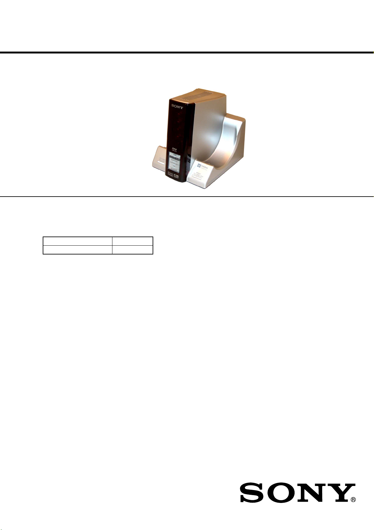
• The DP-IF3000 is the digital surround
processor that comprises the MDRDS3000.
Manufactured under licence from Dolby Laboratories and Digital Theater Systems, Inc.
“Dolby,” “Pro Logic” and the double-D symbol a are trademarks of Dolby Laboratories.
“DTS” and “DTS VIRTUAL ” are trademarks of Digital Theater Systems, Inc.
• MDR-DS3000 consists of the following models respectively.
Cordless stereo headphones MDR-IF3000
Digital surround processor DP-IF3000
US Model
Canadian Model
AEP Model
UK Model
E Model
Tourist Model
SPECIFICATIONS
Decoder functions Dolby Digital
Virtual sound function OFF
Modulation System FM-IM (Based on IEC)
Secondary carrier wave frequency
Transmission distance Approx. 7 m (23 ft.) to the front
Transmission range 20 – 20,000 Hz
Distortion rate 1% or less (1 kHz)
Audio inputs Optical input
Power requirements DC 9 V (from the supplied AC power
Dimensions Approx. 145 x 150 x 146 mm
Mass Approx. 370 g (14 oz.)
Dolby Pro Logic II
DTS
CINEMA
MUSIC
Right channel 2.8 MHz
Left channel 2.3 MHz
(rectangular-type) x 1
Analogue input (pin jack left/right) x 1
adaptor)
(5 3/4 x 6 x 5 3/4 in.)
(w/h/d)
9-961-273-02
2004B02-1
© 2004.02
DIGITAL SURROUND PROCESSOR
Sony Corporation
Personal Audio Company
Published by Sony Engineering Corporation
1
Page 2

DP-IF3000
Notes on Chip Component Replacement
• Never reuse a disconnected chip component.
• Notice that the minus side of a tantalum capacitor may be
damaged by heat.
r
UNLEADED SOLDER
Boards requiring use of unleaded solder are printed with the leadfree mark (LF) indicating the solder contains no lead.
(Caution: Some printed circuit boards may not come printed with
the lead free mark due to their particular size.)
: LEAD FREE MARK
Unleaded solder has the following characteristics.
• Unleaded solder melts at a temperature about 40°C higher than
ordinary solder.
Ordinary soldering irons can be used but the iron tip has to be
applied to the solder joint for a slightly longer time.
Soldering irons using a temperature regulator should be set to
about 350°C.
Caution: The printed pattern (copper foil) may peel away if
the heated tip is applied for too long, so be careful!
• Strong viscosity
Unleaded solder is more viscous (sticky, less prone to flow)
than ordinary solder so use caution not to let solder bridges
occur such as on IC pins, etc.
• Usable with ordinary solder
It is best to use only unleaded solder but unleaded solder may
also be added to ordinary solder.
TABLE OF CONTENTS
1. GENERAL ............................................................................ 3
2. DISASSEMBLY
2-1. Cabinet (Lower) Assy, Luminous Window Assy,
IF Board ............................................................................... 5
2-2. Digital Board ........................................................................ 6
3. ELECTRICAL ADJUSTMENTS
Oscillation Frequency Adjustment .......................................... 7
RF Level Adjustment............................................................... 7
4. DIAGRAMS
4-1. Block Diagrams ................................................................... 9
4-2. Printed Wiring Board – Digital Section (Side A) – ........... 10
Printed Wiring Board – Digital Section (Side B) – ........... 11
4-3. Schematic Diagram – Digital (1/2)Section – .................... 12
4-4. Schematic Diagram – Digital (2/2)Section – .................... 13
4-5. Printed Wiring Board – IF Section – ................................. 14
4-6. Schematic Diagram – IF Section –.................................... 15
4-7. IC Pin Function Description ............................................. 16
4-8. IC Block Diagram ............................................................. 20
5. EXPLODED VIEW
5-1. Processor Section .............................................................. 21
6. ELECTRICAL PARTS LIST......................................... 22
r
Repair DP-IF3000 with MDR-IF3000.
2
Page 3
SECTION 1
GENERAL
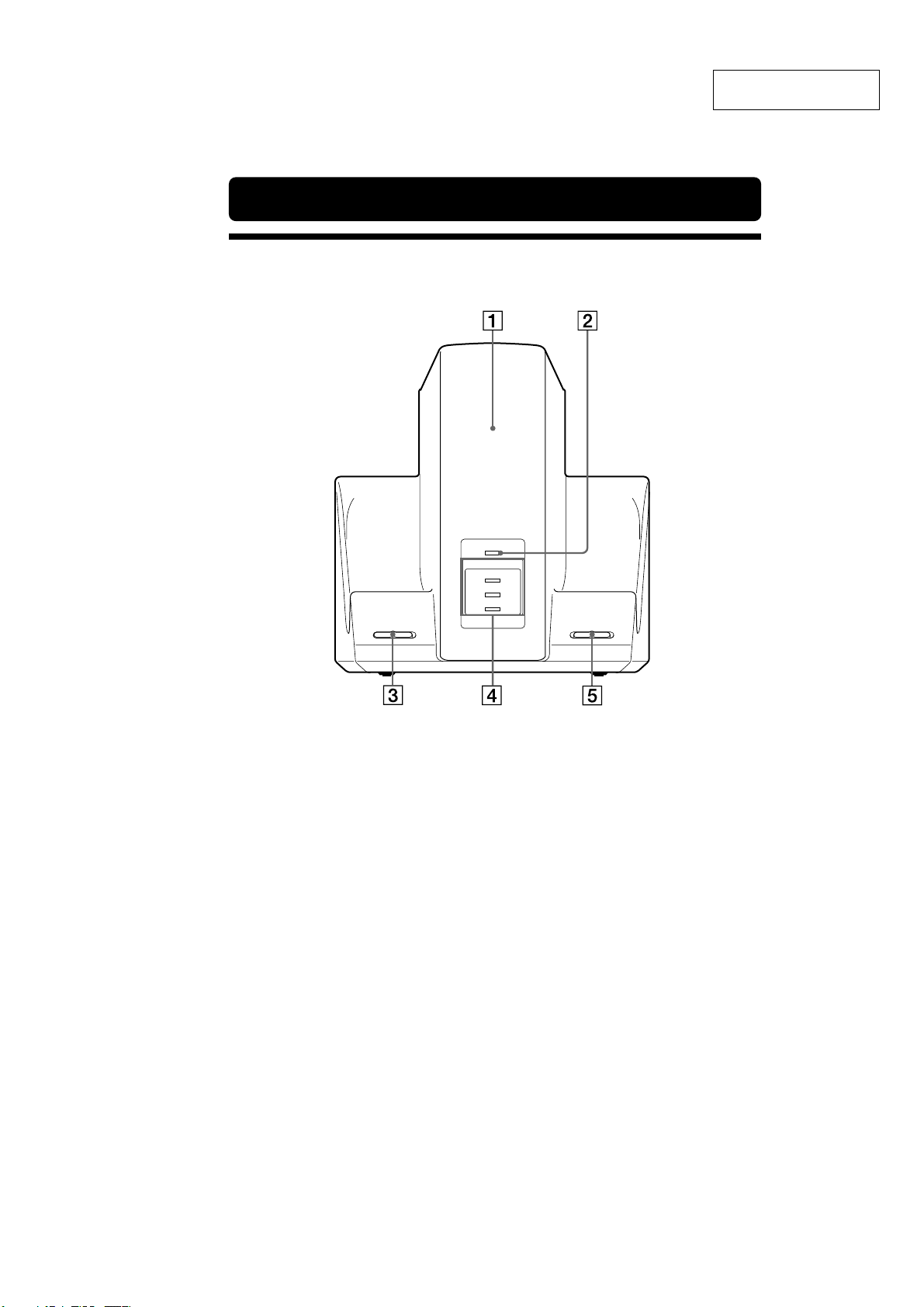
Location and Function of Parts
Front Panel
DP-IF3000
This section is extracted
from instruction manual.
INPUT SELECT
DIGITAL
1 Infrared emitte r
Set the emitter in a position so that there
is a straight, unobstructed path to the
sensor.
2 CHG indica tor
Lights red while charging.
3 INPUT SE LECT switch
Slide to select the input source
(DIGITAL/ANALOG) .
ANALOG
CHG
DECODE MODE
DOLBY DIGITAL
DOLBY PRO LOGIC II
DTS
EFFECT
4 DECODE MODE indica tor
5 EFFECT switch
Slide to select the sound field (OFF/
CINEMA/MUSIC).
MUSICCINEMAOF F
3
Page 4
DP-IF3000
This section is extracted
from instruction manual.
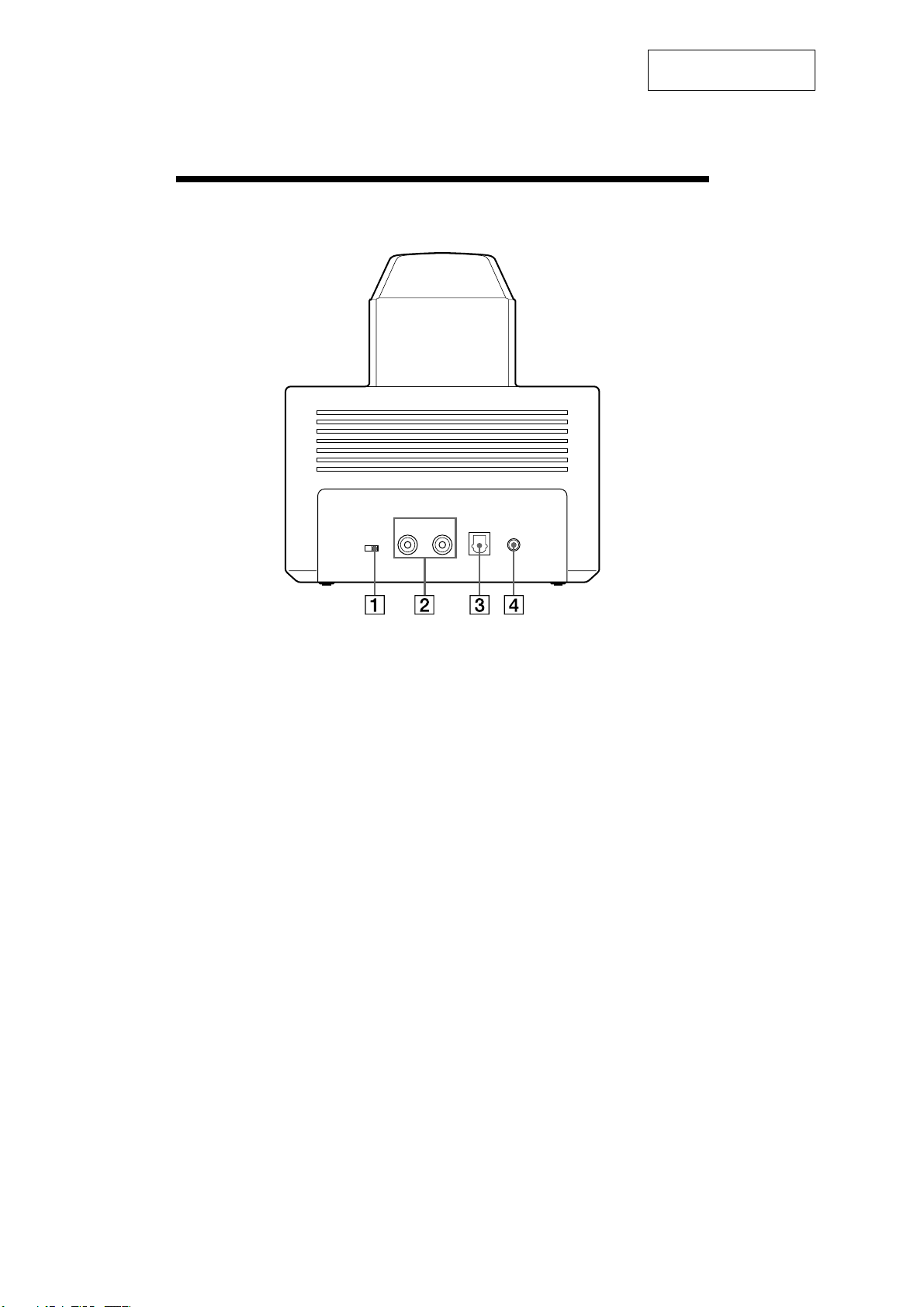
Rear Pane l
1 ATT (attenu ator) switch
Set this switch to “0dB” if the volume is
too low at analogue input. Normally, this
switch should be set to “-8dB”
2 LINE IN jacks
Connect the audio output jacks on audio
or video component (sold separately),
such as a video cassette player or TV, to
these jacks.
ATT
0dB- 8dB
R
LINE IN
DIGITAL IN
L
3 DIGITAL IN jack
Connect a DVD player, or other digital
component (sold separately) to this jack.
4 DC IN 9V jack
Connect the supplied AC power adaptor
to this jack. (Be sure to use the supplied
AC power adaptor. Using products with
different plug polarity or other
characteristics can cause a malfunction.)
DC IN 9V
4
Page 5
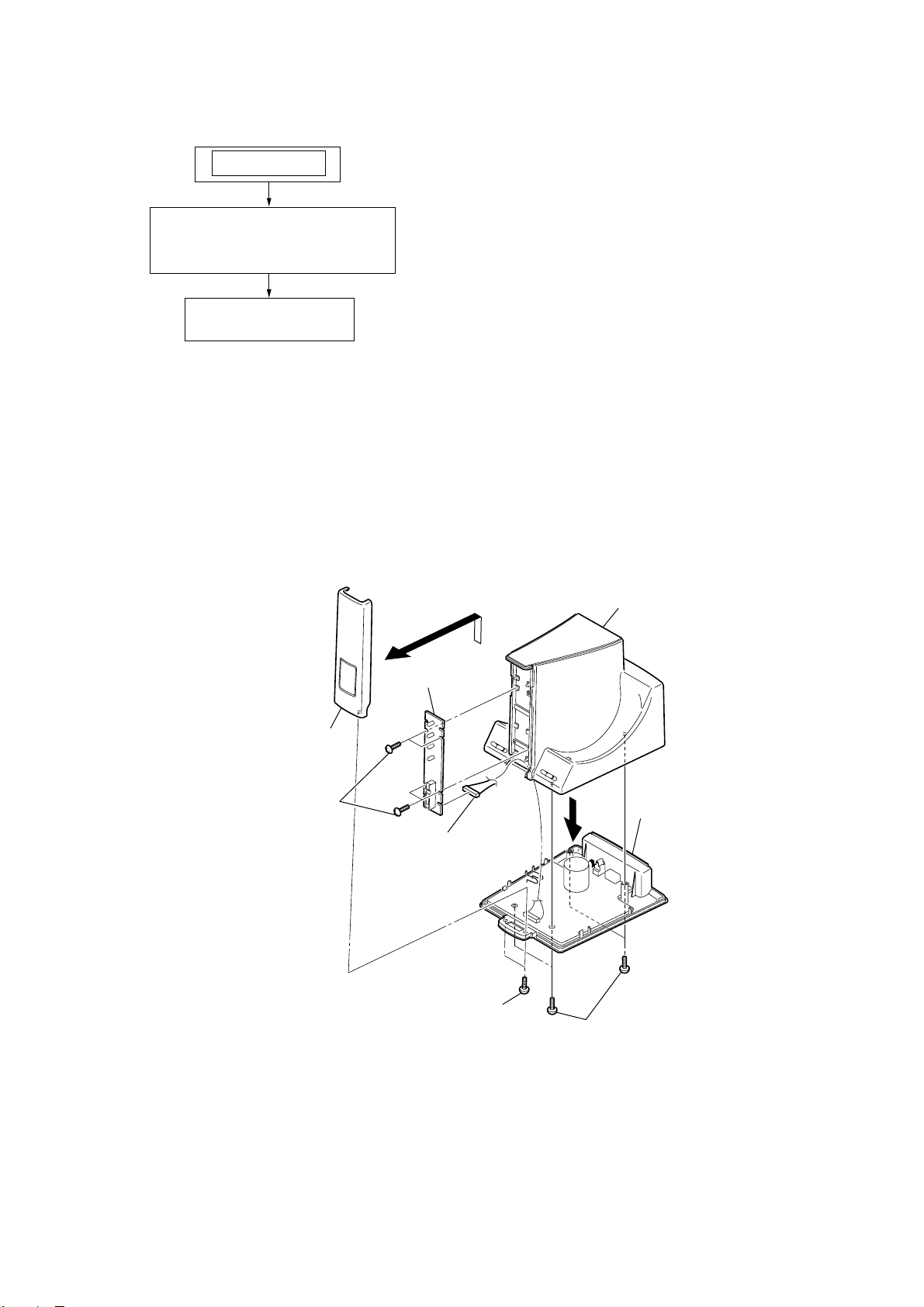
SECTION 2
y
DISASSEMBLY
Note : This set can be disassemble according to the following sequence.
SET
CABINET (LOWER) ASSY,
LUMINOUS WINDOW ASSY,
IF BOARD
DIGITAL BOARD
Note : Follow the disassembly procedure in the numerical order given.
DP-IF3000
2-1. CABINET (LOWER) ASSY, LUMINOUS WINDOW ASSY, IF BOARD
cabinet (upper)
6
9
IF board
7
luminous window assy
8
four screws (+B2.6)
4
connector (CN501)
3
5
cabinet (lower) ass
2
two screws (+B2.6)
1
four screws (+B2.6)
5
Page 6
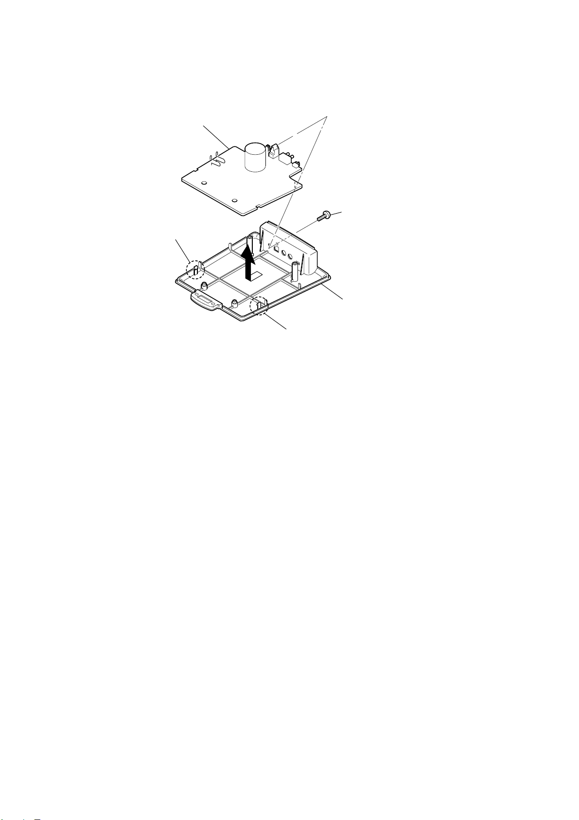
DP-IF3000
)
2-2. DIGITAL BOARD
4
DIGITAL board
2
claw
3
1
screw (+B3
cabinet (lower)
2
claw
6
Page 7
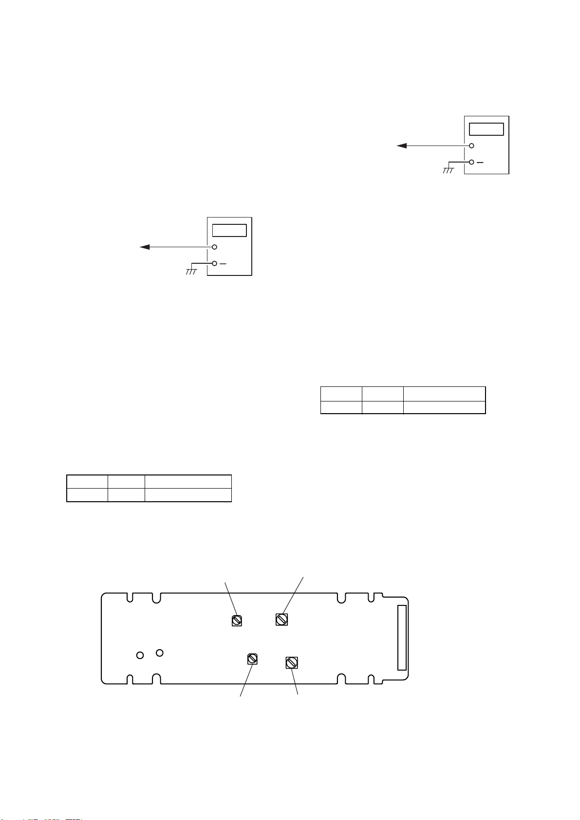
SECTION 3
y
r
ELECTRICAL ADJUSTMENTS
DP-IF3000
Notes:
1. These adjustments are performed in the order that they are described.
2. Adjustment and measurement are performed for each channel
unless otherwise specified.
3. Adjustment is made for the left channel first and then the right
channel.
4. The power voltage is supplied with 9V.
Oscillation Frequency Adjustment
setting:
digital frequenc
counter
IF board
TP513 (L-ch)
TP514 (R-ch)
+
Adjustment method:
• Perform this adjustment without signal.
1. S202(INPUT SELECT) is set on the DIGITAL side, and there
is no input signal in IC001(DIGITAL IN)(to set the mute state).
Note:
Adjustment can’t be done any more because the luminosity of
LED stops when condition without an input signal lasts for more
than ten minutes.
Move S202(INPUT SELECT) to the ANALOG side, and move ATT
SW(S051) in your making LED light sent out again.
2. Connect a digital frequency counter to TP513 for L-ch and
TP514 for R-ch on the IF board.
3. Adjust L503 (L-ch) and L501 (R-ch) on the IF board so that
the reading on the digital frequency counter is each within 2.3
MHz (L-ch) and 2.8 MHz (R-ch).
RF Level Adjustment
setting:
digital voltmete
IF board
TP513 (L-ch)
TP514 (R-ch)
+
Adjustment method:
• Perform this adjustment without signal.
1. S202(INPUT SELECT) is set on the DIGITAL side, and there
is no input signal in IC001(DIGITAL IN)(to set the mute state).
Note:
Adjustment can’t be done any more because the luminosity of
LED stops when condition without an input signal lasts for more
than ten minutes.
Move S202(INPUT SELECT) to the ANALOG side, and move ATT
SW(S051) in your making LED light sent out again.
2. Connect a digital volmeter to TP513 for L-ch and TP514 for
R-ch on the IF board.
3. Adjust RV501 (L-ch) and RV502 (R-ch) on the IF board so
that the reading on the digital volmeter is 490mV.
Specified Value:
L-ch RV501 487.5 to 492.5 mV
R-ch RV502 487.5 to 492.5 mV
Specified Value:
L-ch L503 2.298 to 2.302 MHz
R-ch L501 2.798 to 2.802 MHz
Adjustment Location:
RF Level Adjustment
– IF board (side A) –
TP514
TP513
RF Level Adjustment
RV502
(R-CH)
RV501
(L-CH)
L501
Oscillation Frequency Adjustment
(R-CH)
CN501
L503
Oscillation Frequency Adjustment
(L-CH)
7
Page 8
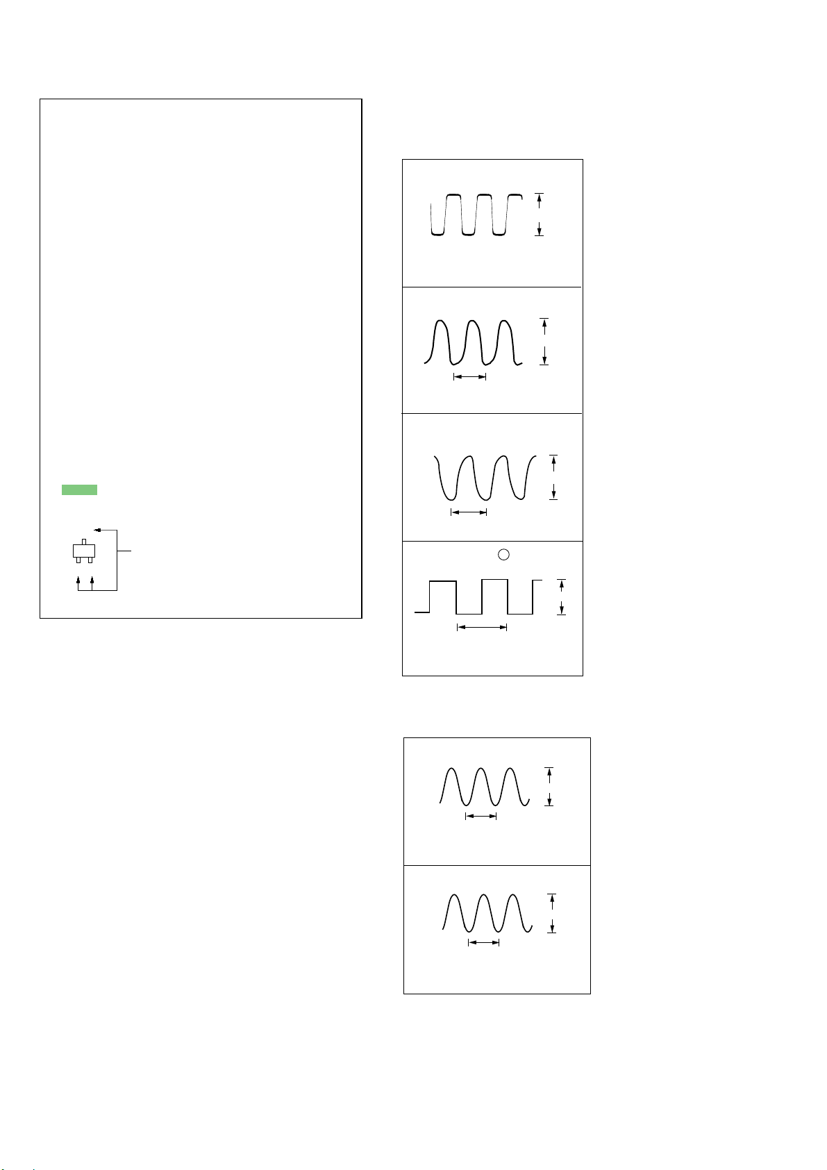
DP-IF3000
p
p
p
THIS NOTE IS COMMON FOR PRINTED WIRING
BOARDS AND SCHEMATIC DIAGRAMS.
(In addition to this, the necessary note is
printed in each block.)
SECTION 4
DIAGRAMS
r
WAVEFORMS
– DIGITAL BOARD –
for schematic diagram:
• All capacitors are in µF unless otherwise noted. pF: µµF
50 WV or less are not indicated except for electrolytics
and tantalums.
• All resistors are in Ω and
specified.
•%: indicates tolerance.
• C : panel designation.
• A : B+ Line.
• H : adjustment for repair.
• Power voltage is dc 9 V and fed with regulated dc power
supply from external power voltage jack.
•Voltage is dc with respect to ground under no-signal
(detuned) conditions.
•Voltages are taken with a VOM (Input impedance 10 MΩ).
Voltage variations may be noted due to normal production tolerances.
• Signal path.
F : ANALOG
J : RF
c : DIGITAL
for printed wiring boards:
• X : parts extracted from the component side.
• : Pattern from the side which enables seeing.
C
Q
B
E
These are omitted.
1
4
/
W or less unless otherwise
IC002 wa XOUT
1
12.288 MHz
IC201 ia X1
2
250 nsec
IC1201 ol MCLK
3
80 nsec
IC1201 LRCK0
4
3.5 Vp-
VOL/DIV : 1V AC
TIME/DIV : 50nsec
3.5 Vp-p
VOL/DIV : 1V AC
TIME/DIV : 0.1
3.2 Vp-p
VOL/DIV : 1V AC
TIME/DIV : 50nsec
108
µ
sec
21 µsec
– IF BOARD –
Q501 E
1
0.44 µsec
Q507 E
2
0.36 µsec
3.5 Vp-
VOL/DIV : 1V AC
TIME/DIV : 5
VOL/DIV : 0.5V AC
TIME/DIV : 0.2
VOL/DIV : 0.5V AC
TIME/DIV : 0.2 µsec
µ
1.7 Vp-p
1.7 Vp-
sec
µ
sec
8
Page 9
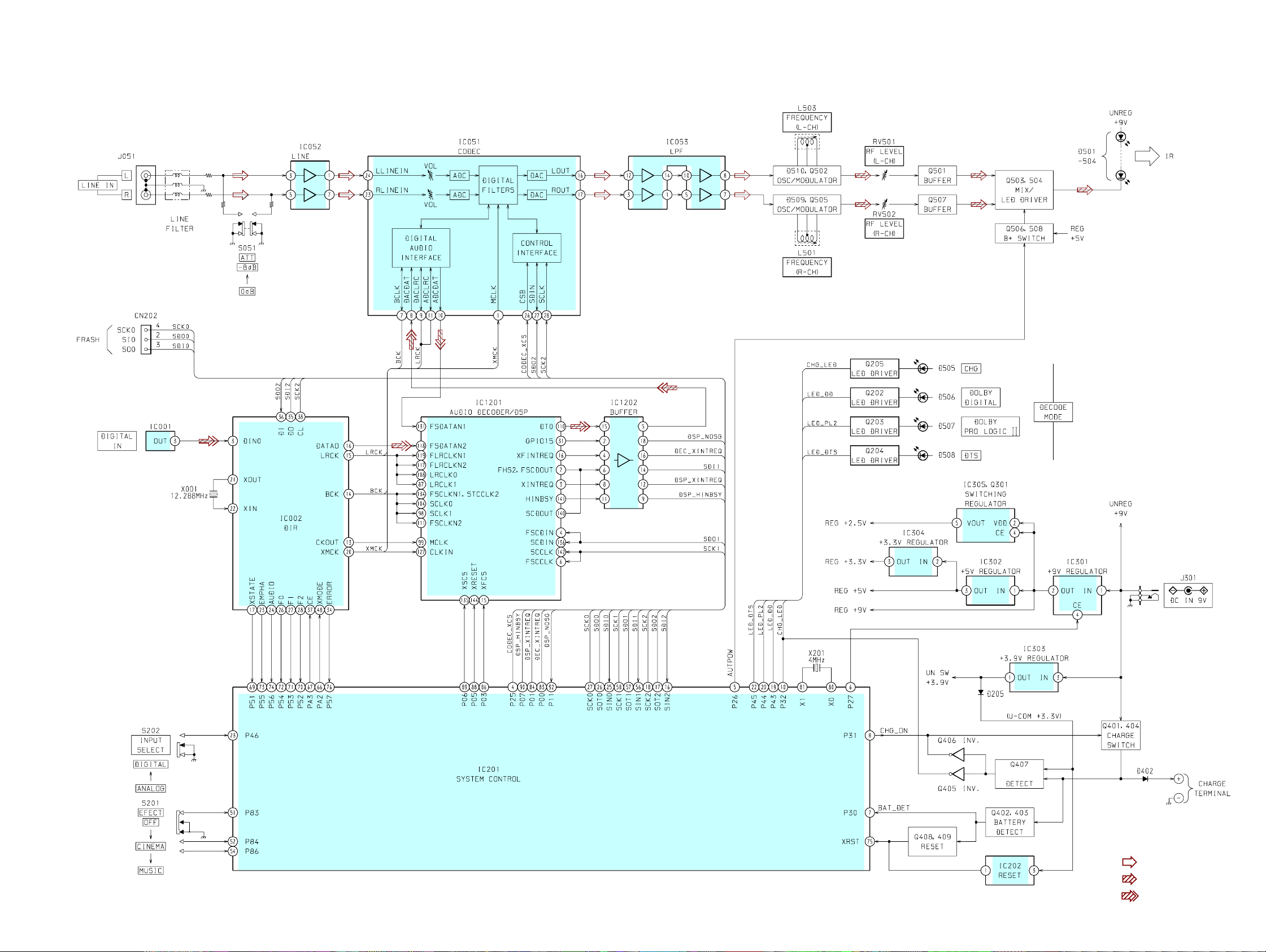
4-1. BLOCK DIAGRAMS
LF051
DP-IF3000
AMP
99
BATT-SHORT
• Signal Path
: ANALOG
: RF
: DIGITAL
Page 10

DP-IF3000
4-2. PRINTED WIRING BOARD — DIGITAL SECTION (SIDE A) —
1
DIGITAL BOARD
2
(SIDE A)
A
B
C1223
L1203
C1211
R1243
R1244
R1245
36
37
C
C1214
C1215
C1216
R1249
C1217
72
R087
C082
C086
C083
R088
8
7
C085
73
C088
IC053
L010
C087
C019
L058
C052
L011
C062
D
E
R073
C079
R069
L1204
R081
R090
R079
R080
C076
C080
C1222
C092
R091
C078
1
R083
R089
R084
14
F
R086
C090
C1210
C095
L059
IC1201
L052
15
21
C094
G
L060
3 4 5 6 7
C1221
R1228
R1219
C1209
R1217
R1238
R1230
R052
28
R063
C093
R1236
R053
8
R1233
R1235
C1208
R054
R055
7
1
R064
R065
R070
1
108
R1218
C060
R067
R066
C069
R078
R1240
R051
14
IC051
22
R1262
144
109
C054
• : Uses unleaded solder.
C089
C1224
L1205
C006
R068
8
1
C059
L055
R023
R021
R020
R022
C064
6
1
L054
20
C1206
R1214
C1201
R009
C008
R075
5
4
R056
LF051
L053
11
C005
R015
R016
R018
C007
R057
C002
IC052
C056
C1203
C1205
C1202
L1202
C016
L051
D052
L1207
R1221
R1220
R1215
R074
1
10
C1220
R1216
R1227
C1204
C1207
R1212
R1202
R076
R062
R071
IC1202
L1201
C009
L056
C071
R059
R077
C067
R1201
R017
R024
R024
4
3
C1218
R1260
R008
1
12
L057
C018
R060
D051
R006
R007
48
IC002
13
L008
L007
L005
L004
L006
C017
R058
C021
C208
C207
R005
C011
D057
D056
L202
C217
C210
R229
R224
C003
C013
D205
R004
37
24
R019
C020
C216
L009
R010
R003
36
R012
R013
25
L062
C221
IC202
R271
R273
L003
C012
C222
SL203
X201
R002
R001
R011
C004
Q205
C015
D055
D053
100
R014
L001
D054
8
Q202
C219
Q203
C218
Q204
C220
R270
R274
C204
R236
R206
C212
75
76
R275
C205
R276
IC201
1
R267
R210
C211
C202
C206
R228
L201
C224
Q408
R222
C209
C402
R223
C223
R408
Q402
Q403
R410
R413
51
50
R220
R221
26
25
Q409
Q405
Q407
C403
Q406
D
G
D401
C401
L402
S
R411
Q404
R412
R409
D402
Q401
L401
9
+
CHARGE
TERMINAL
–
• Semiconductor
Location
Ref. No. Location
D051 G-4
X001
L303
C316
5
1
IC305
C308
D302
L301
1
3
4
Q301
4
6
3
C315
C310
1
3
IC304
1
R402
3
C311
C312
IC303
C305
R403
R404
R405
R406
R407
D052 G-4
D053 G-5
D054 G-5
D055 G-5
D056 G-5
D057 G-5
D205 B-5
D301 G-7
D302 D-7
D401 C-8
D402 C-8
IC002 D-5
IC051 E-3
IC052 F-4
IC053 F-2
IC201 C-6
IC202 B-5
IC303 F-7
IC304 E-8
IC305 E-7
R301
C301
IC1201 C-3
IC1202 B-4
Q202 A-6
D301
Q203 A-6
Q204 A-6
Q205 A-5
C001
C014
L002
C303
Q301 E-7
Q401 C-8
Q402 C-8
Q403 C-8
Q404 C-8
Q405 A-8
Q406 A-8
LF301
1-860-186-
12
(12)
Q407 B-8
Q408 D-7
Q409 D-7
1010
Page 11

DP-IF3000
PRINTED WIRING BOARD — DIGITAL SECTION (SIDE B) —
1
A
B
N.C
DIGITAL BOARD
2
DIGITAL ANALOG
CN202
(SIDE B)
S202
INPUT SELECT
t
SL202
SL201
C
3 4 5 6 7
C213
• : Uses unleaded solder.
IF
A
BOARD
(Page 14)
CNP201
C214
C010
S201
EFFECT
OFF CINEMA MUSIC
tt
C1212
8
9
D
• Semiconductor
Location
Ref. No. Location
C318
C055
C063
C1213
C077
C073
C074
C075
C313
E
C306
F
IC302
3
1
C314
C309
C302
C307
C317
C304
C053
C072
C058
C070
C061
C051
C068
C066
IC001 G-4
IC301 F-2
IC302 F-2
IC301
C057
G
J301
DC IN 9V
1
3
C065
IC001
1-860-186-
DIGITAL IN
H
LR
J051
LINE IN
S051
t
-8dB 0dB
ATT
12
(12)
11 11
Page 12

DP-IF3000
4-3. SCHEMATIC DIAGRAM — DIGITAL (1/2) SECTION —
(Pageg 13)
(Pageg 15)
MCKCODEC
BCK
DSPOUT
LRCK
ADDATA
J051
LINE IN
R067
100
C061
C060
R055
10
16V
0.1
CNP201
12P
1k
R054
R051
1k
1k
MA3075WA
D052
C051
10
16V
C054
0.1
R053
1k
MA3075WA
1SS355TE-17
D053
R052
L053
0µH
D051
L054
0µH
C094
0.01
C093
0.01
L055
1k
0µH
XDTS_LED
R065
1k
R066
1k
LF051
COM MODE
L051
LINE
FILTER
D054
1SS355TE-17
C021
C020
0.1
0.1
SCK2
C067
100p
XDD_LED
XPL2_LED
SDO2
CODEC_XCS
CODEC
AUTPOW
XCHG_LED
R070
10k
R064
100
R063
10k
C056
100p
SLIDE SWITCH
R077
680k
1SS355TE-17
MA3130WA
R071
D056
D055
DGND
L301
22µH
L402
10µH
_3.9V
UNSW
C401
0.1
IC305
XC6365A253MR
SWITCHING
REGULATOR
REG_2.5V
C318
TP404
TP405
LF301
L303
47µH
C317
C316
33
10V
2200
0.1
6.3V
CHARGE
(
TERMINAL
J301
DC IN 9V
(
C304
BUS
Q406
DTC144EKA
R411
INV.
R412
5.6
RB051L-40TE25
RTQ035P02TR
100
16V
S
R409
4.7k
RB501V-40-TE-17
R408
100k
DTC144EKA
D301
Q301
SWITCHING
REGULATOR
C315
0.1
4.7k
D402
Q409
RESET
D302
RB161M-20FTR
Q404
DTC144EKA
CHARGE
SWITCH
L401
10µH
C403
2.2
Q403
DTC144EKA
BATTERY
DETECT
CHG_ON
Q407
2SK3019
CHARGE-UP
DETECT
R413
10k
R407
22k
Q402
DTA144VKA
BATTERY
DETECT
C402
0.1
25V
C314
C308
0.1
REG_5V
C1223
C089
0.1
0.001
L011
C076
C088
820p
0.1
R087
R088
10k
10k
0µH
C086
270p
C085
270p
C075
100
10V
IC302
KIA78S05P-TP
+5V REGULATOR
L010
0µH
C087
820p
SL305
C309
100
16V
R089
L058
15µH
C312
0.1
IC301
PQ09RD11
+9V REGULATOR
10k
R086
10k
C095
0.1
C313
100
10V
R301
10k
R081
R073
22k
MAPOW
L057
L059
µH
100
R069
C306
100
6.3V
C018
0.1
C017
0.1
C302
220
100
16V
C058
10
16V
R058
9.1k
D057
1SS355TE-17
R062
C066
R074
9.1k
L060
10µH
C016
0.1
C063
10
16V
C062
0.1
C074
L052
10
50V
15µH
C073
10
50V
C052
0.1
C055
10
16V
C053
10
16V
R056
22k
C057
R059
22
43k
VCC
L062
10µH
16V
IC052
NJM4558M-TE2
LINE AMP
C065
22
16V
C070
100
C071
16V
C068
R078
47k
L056
0.1
15µH
C069
100
0.1
10V
C059
100p
22k
VEE
10
R076
16V
22k
C064
100p
R068
43k
R075
22k
C072
10
16V
L051
15µH
R057
680k
R060
47k
47k
S051
2C-2P
ATT
-8dB
0dB
2.2k
C077
100
10V
C078
0.1
R080
47k
C019
0.1
IC053
NJM2112V
22k
R079
2.2k
IC304
XC6206P332PR
+3.3V REGULATOR
C311
0.1
C305
0.1
C079
0.0018
C092
0.0068
R091
100
C083
100p
R084
11k
R083
11k
C082
100p
R090
100
C090
0.0068
C080
0.0018
C301
0.1
XRST
U-COM3.3V
BAT_DET
XC6202P392PR
+3.9V REGULATOR
C310
0.1
CHG_LED
R410
10k
C303
0.1
IC303
DTC144EKA
R406
R405
R404
R403
R402
DTA144EKA
Q405
INV.
D401
RD5.6SB-T1
Q401
2SB1424
CHARGE
SWITCH
560
560
560
470
470
Q408
RESET
C307
100
10V
15000
1212
Page 13

DP-IF3000
• See page 16 for Pin Function Description.4-4. SCHEMATIC DIAGRAM — DIGITAL (2/2) SECTION —
(Page 12)
IC001
JFJ4000
-01SY
DIGITAL
IN
DTS_LED
X
XPL2_LED
DD_LED
X
AUTPOW
REG_2.5V
U-COM
CHG
XCHG_LED
UNSW
REG_5V
BUS
XRST
_LED
_3.9V
DGND
C1203
0.1
1216
R
3.3k
SCK1
_XRST
DSP
X001
CX-49G
L005
L006
L007
L008
Hz
SDI1_L
DSP_HINBSY_L
0µH
0µH
0µH
0µH
C1214
L004
0µH
R021
R022
R023
R024
C1220
0.001
R1227
10k
1215
C1209
C1211
0.1
R
0.1
C1212
6.3V
R
10k
R1217
3.3k
R1228
3.3k
R1233
3.3k
1238
3.3k
R1240
3.3k
R1243
3.3k
R1244
3.3k
R1245
3.3k
470
L1203
µH
10
C1221
0.1
C012
C013
20p
20p
12.288M
R019
1M
018
R
33k
1220
R
3.3k
R1221
_L
EQ
SP_XINTR
D
O1
SD
1
SCK
I1_L
SD
EC_XCS
D
EQ_L
DEC_XINTR
Q204
DTC123YUA
Q202
A
TC123YU
D
AUTPOW
C218
0.001
3.3V
C015
0.1
C014
0.1
L002
C001
µH
10
0.47
L001
0µH
BK2125
L003
µH
15
DIR_XCS
SCK2
DIN0
IR_XR
D
C219
0.001
Q202-205
LED DR
L009
ST
LED_DD
0µH
Q203
UA
TC123Y
D
LED_PL2
C220
0.001
IVER
R010
10k
R001
0
R002
0
R003
10k
R004
10k
C003
0.1
R005
10k
R006
10k
R007
10k
R008
10k
R009
10k
C002
0.01
C005
0.1
C007
0.1
LED_DTS
DSP_NOSG_L
C1222
R011
0
R012
0
C010
47
10V
SDO2
0.1
C004
0.1
SDI2
014
R
10k
DIR_ERR
R013
0
LC89056W
C006
0.01
DIN0
R015
1219
R
0
3.3k
1235
R
3.3k
1236
R
10k
C1213
L1204
100
µH
10
10V
DIR_F1
DIR_F0
DIR_F2
IC002
-E
016
5.6k
R
4.7k
C008
0.01
017
R
100
C009
0.1
C1204
1201
R
0
BCK
SDO1
DSP_XCS
0.1
DIR_NAUD
DIR_EM
R020
100
DIR_XST
330
DIRDATA
330
330
330
CKCOD
M
0.1
LRCK
XRST
C1205
C1206
DER/DSP
EC10DS2TE12R
C214
1000
6.3V
C217
0.1
L202
µH
15
C213
100
10V
C216
0.1
68p
C222
0.1
XC61FN
C1201
0.0012
C1207
2.2
10V
C1216
0.1
D205
C221
0.001
IC202
R
2812M
ESET
R
4.7
6.3V
L1201
µH
15
MCK
ADDATA
IC1201
CS494003-CQ
ECO
D
IO
AUD
C1215
0.1
C011
0.1
P
CK
M
BCK
EC
R271
4.7k
R
R1249
LRCK
1214
10k
3k
DIRDATA
LRCK
R
0.001
C1202
0.1
1202
R
BCK
330
DSPOUT_L
L1202
0.001
A
CHG_LED
C1217
0.1
DSP_XIN
DEC_XINTREQ
C208
C210
0.1
0µH
BK1608
TREQ
DIR_ERR
X201
Hz
4M
DEC_XCS
DSP_XRST
DSP_XCS
DSP_HINBSY
DSP_NOSG
R1212
0
R229
10k
224
10k
C207
Q205
TC123YU
D
210
R
4.7k
BCK
LRCK
CKCODEC
M
1218
R
0
_L
SG
SP_NO
D
EQ_L
DEC_XINTR
T
C1208
0.1
1230
R
0
C1210
0.1
C212
0.1
R273
DSPOU
SDI1_L
DSP_XINTREQ
SP_HINBSY
D
EFF_OFF
EFF_C
EFF_M
SDO0
SDI0
SCK0
P
XRST
_EM
DIR
DIR_NAUD
R206
1k
SL203
0
267
R
10k
_L
DIR_F0
DIR_F1
OW
AUTP
CODEC_XCS
R1262
330
DIR_F2
APOW
M
DIR_XST
BAT_DET
L1207
CHG_ON
0µH
DIR_XCS
DIR_XRST
201
S
EFECT
FF
O
CINEM
USIC
M
B90478PFV-G-
M
158-BNDE1
SYSTEM
CHG_LED
A
IC201
CONTR
C1224
0.1
IC
74LVC244APW
SN
BUFFER
E1
O
R236
10k
OL
SDI2
1202
CN202
C211
L1205
µH
10
R
C1218
EFF_M
LED_DTS
R1260
0
EFF_C
N
0.1
.C
EFF_OFF
SDI0
R270
10k
DSP_N
DEC_XINTR
DSPO
SP_X
D
SP_H
D
274
R
R275
276
R
C202
C204
C205
SDI1
INTR
INBSY_L
R221
10k
SG
O
EQ
UT_L
EQ
10k
10k
10k
0.1
0.1
0.1
R223
SL201
10k
C206
0.1
R222
10k
R220
10k
R228
10k
C224
SL202
0.001
C223
0.001
C209
0.1
L201
0µH
SCK0
SDO0
S202
PUT
IN
S202
SELECT
ITAL
DIG
G
ALO
AN
OE2
5P
1
SDI1
SCK1
SDO
SCK2
SDO2
LED_PL2
LED_DD
0.1
13 13
Page 14

DP-IF3000
4-5. PRINTED WIRING BOARD — IF SECTION —
1
IF BOARD
(SIDE A)
2
A
B
TP513
Q503
TP514
R514
Q504
C
• : Uses unleaded solder.
3 4 5 6 7
C505
C512
R515
R522
R520
Q506
Q508
RV502
R511
R519
R521
RV501
R506
C501
Q507
R508
R502
C514
C507
R512
L502
C510
C511
C518
R528
L504
C509
Q501
C508
C520
C521
C528
R530
R510
C527
R529
Q502
Q505
C519
L501
R527
C506
R509
R516
R526
L503
C504
C517
D510
R504
R505
D509
R507
R517
C516
R518
R503
R513
C523
R501
R523
R524
C530
C531
C532
C533
R525
C534
CN501
1
C529
12
1-860-187-
DIGITAL
BOARD
(Page 11)
12
(12)
8
A
• Semiconductor
Location
Ref. No. Location
D501 E-4
D502 E-3
D503 E-2
D504 E-1
D505 E-6
D506 E-7
D507 E-7
D508 E-7
D509 A-5
D510 C-5
Q501 C-4
Q502 B-5
Q503 C-2
Q504 C-2
Q505 A-5
Q506 C-4
Q507 B-4
Q508 C-4
IF BOARD
(SIDE B)
D
C513
(IR TRANSMITTER)
D504
D503
D502
E
D501
C525
C526
C515
D505
CHG
C502
C503
F
C524
DOLBY PROLOGIC
D506
DOLBY DIGITAL
D507
D508
DTS
1-860-187-
12
(12)
1414
Page 15

4-6. SCHEMATIC DIAGRAM — IF SECTION —
CN501
12P
DP-IF3000
(Page 12)
C534
0.1
C529
0.001
C530
0.001
R513
2.2k
C524
16V
R515
12
D501
DAL5815
D502
DAL5815
D503
DAL5815
D504
DAL5815
TP514
Q504
2SD1664
C505
0.1
C501
0.1
D501-504
IR
TRANSMITTER
Q503,504
MIX/
LED DRIVER
Q503
2SD1664
TP513
R502
1.5k
Q501
2SA1037AK
BUFFER
R514
12
R526
270k
L503
FREQUENCY
(L-CH)
R501
560
R523
560
R524
560
R525
560
Q502
2SC2059
OSC
R527
100
CHG
DTS
DOLBY
DIGITAL
DOLBY
PRO
LOGIC
C518
2200p
C525
47
16V
R528
2.2k
C527
0.1
DECODE
MODE
82µH
C519
47p
L504
C520
12p
RV501
2.2k
RF LEVEL
(L-CH)
C521
56p
R506
0.5%
C509
0.0022
R508
2.7k
0.5%
30k
D510
B
D505
SLR342VC3F
D506
SLR342VC3F
D507
SLR342VC3F
D508
SLR342VC3F
C517
12p
C531
0.001
C513
22
16V
C515
47
16V
C523
47
0.1
C532
0.001
R529
1k
R516
3.9k
R517
3.9k
R518
0.001
22k
C533
SVC203CP-T
C516
3300p
R503
3.3k
C502
22
16V
C503
16V
R512
2.2k
C528
0.1
C512
0.1
C508
39p
C510
10p
L502
68µH
R520
10k
DTA114EKA
B+ SWITCH
Q508
C511
47p
RV502
2.2k
RF LEVEL
(R-CH)
Q506
DTC114YKA
LEVEL
DETECT
C522
C514
0.0022
C526
C507
2200p
16V
47
R522
10k
R530
1k
C506
10p
FREQUENCY
(R-CH)
L501
R509
270k
Q505
2SC2059
OSC
R510
100
R507
47
22k
R505
3.9k
R504
3.9k
C504
3300p
D509
SVC203CP-T
B
R519
30k
0.5%
R511
2.7k
0.5%
R521
1.5k
Q507
2SA1037AK
BUFFER
15 15
Page 16

DP-IF3000
4-7. IC Pin Function Description
• IC1201 CS494003-CQ AUDIO DECODER/DSP (DIGITAL BOARD)
Pin No.
1 UHS0 I Mode select signal
2 UHS1 I Mode select signal
3 XINTREQ O DSP interruption request signal for MB90478
4 FSCDIN I Serial data signal input from MB90478
5 GPIO20 — Npt used (Open)
6 FSCCLK I Serial clock signal input from MB90478
7 FHS2,FSCDOUT O Serial data output for MB90478
8 GPIO21 — Npt used (Open)
9 FDAT7 — Npt used (Open)
10 VDD6 — Power supply (+2.5V)
11 VSS6 — Ground
12 FHS0 I Mode select signal (Pull up)
13 FHS1 I Mode select signal (Pull down)
14 FDAT6 — Npt used (Open)
15 XFCS I DEC chip select signal from MB90478
16 XFINTREQ O DEC interruption request signal for MB90478
17 FDBCK — Npt used (Pull up)
18 FDAT5 — Npt used (Open)
19 FDAT4 — Npt used (Open)
20 VDD7 — Power supply (+2.5V)
21 VSS7 — Ground
22 FDAT3 — Npt used (Open)
23 FDBDA — Npt used (Pull up)
24 FDAT2 — Npt used (Open)
25 DBDA — Npt used (Pull up)
26 DBCK — Npt used (Pull up)
27 FDAT1 — Npt used (Open)
28 TEST I Test terminal (Connected to ground)
29 FDAT0 — Npt used (Open)
30 GPIO16 — Npt used (Open)
31 GPIO15 O DSP NOSG signal output for MB90478
32 GPIO14 — Npt used (Open)
33 WE — Npt used (Open)
34 to 38 D0 to D4 — Npt used (Open)
39 DQM0 — Npt used (Open)
40 D5 — Npt used (Open)
41 VSSSD4 — Ground
42 VDDSD4 — Power supply (+3.3V)
43,44 D6,D7 — Npt used (Open)
45 DQM1 — Npt used (Open)
46,47 A18,A17 — Npt used (Open)
48 NC5 — Npt used (Connected to ground)
49 A16 — Npt used (Open)
50 VSSSD3 — Ground
51 VDDSD3 — Power supply (+3.3V)
52 to 56 A15 to A11 — Npt used (Open)
57 VSSSD2 — Ground
58 VDDSD2 — Power supply (+3.3V)
59 CLKOUT — Npt used (Open)
60 A9 — Npt used (Open)
61 CLKIN I Npt used (Pull up)
62,63 A8,A7 — Npt used (Open)
64 CLKEN — Npt used (Open)
Pin Name
I/O
Description
Pin No.
65 to 67 A6 to A4 — Npt used (Open)
68 SD_CS — Npt used (Open)
69 VSSSD1 — Ground
70 VDDSD1 — Power supply (+3.3V)
71 to 76 A19 to A10,A0 to A3 — Npt used (Open)
77 RAS — Npt used (Open)
78 CAS — Npt used (Open)
79 to 82 GPIO27 to GPIO24 — Npt used (Open)
83,84 NC4,NC3 — Npt used (Connected to ground)
85,86 GPIO23,GPIO22 — Npt used (Open)
87 LRCLK1 I Sample rate clock signal input from LC89056W
88,89 NC2,NC1 — Npt used (Connected to ground)
90 VDD1 — Power supply (+2.5V)
91 VSS1 — Ground
92 to 94 GPIO31 to GPIO29 — Npt used (Open)
95 to 97 GPIO7 to GPIO5 — Npt used (Open)
98 SCLK1 I Serial clock signal input from LC89056W
99 MCLK I Master clock signal input from LC89056W
100 VDD2 — Power supply (+2.5V)
101 VSS2 — Ground
102 GPIO28 — Npt used (Open)
103 GPIO4 — Npt used (Open)
104 SCLK0 I Serial clock signal input from LC89056W
105 GPIO3 — Npt used (Open)
106 XMT958A — Npt used (Open)
107 DT2 — Npt used (Open)
108 LRCK0 I Sample rate clock signal input from LC89056W
109 DT1 — Npt used (Open)
110 DT0 O Digital data output for WM8734EFL
111 FSCLKN2 I Serial clock signal input from LC89056W
112 GPIO2 — Npt used (Open)
113 VSS3 — Ground
114 VDD3 — Power supply (+2.5V)
115,116 GPIO1,GPIO0 — Npt used (Open)
117 FLRCLKN2 I Sample clock signal input from LC89056W
118FSDATAN2 I Digital data input from LC89056W
119 FLRCLKN1 I Sample rate clock signal input from LC89056W
120,121 GPIO10,GPIO11 — Npt used (Open)
122 PLLVSS — Ground
123 FILT2 — PLL filter connecting terminal
124 FILT1 — PLL filter connecting terminal
125 PLLVDD — Power supply (+2.5V)
126 XTALO — Npt used (Open)
127 CLKIN I Master clock signal input from LC89056W
128 CLKSEL I DSP clock select (Connected to ground)
129 GPIO9 — Npt used (Open)
130 GPIO13 — Npt used (Open)
131 FSDATAN1 I Serial A/D data input XWM8734EFL
132 VDD4 — Power supply (+2.5V)
133 VSS4 — Ground
134 FSCLKN1,STCCLK2 I Serial clock signal input from LC89056W
135 XSCS I DSP chip select signal input frpm MB90478
136 SCDIN I Serial data input from MB90478
Pin Name
I/O
Description
1616
Page 17

DP-IF3000
Pin No.
137 VSS5 — Ground
138 VDD5 — Power supply (+2.5V)
139 GPIO12 — Npt used (Open)
140 SCDOUT O Serial data output for MB90478
141 HINBSY O DSP HINBSY signal for MB90478
142 SCCLK I Serial control port clock input
143 UHS2 I Mode select signal (Pull up)
144 XRESET I DSP reset signal input from MB90478
Pin Name
I/O
Discription
17
Page 18

DP-IF3000
• IC201 MB90478PFV-G-158-BNDE1 SYSTEM CONTROL (DIGITAL BOARD)
Pin NamePin No. I/O
1 to 3 P22 to P24 — Not used (Open)
4 P25 O Chip select signal output for WM8734EFL
5 P26 O IR LED drive power supply ON/OFF signal output
6 P27 O REG+9V main power supply ON/OFF signal output
7 P30 I Battery voltage level detection signal input
8 P31 O Battery charge ON/OFF signal output
9 VSS — Ground
10 P32 O CHG LED drive signal output
11 to 15 P33 to P37 — Not used (Open)
16 SIN2 I Serial data input from LC89056W
17 SOT2 O Serial data output for XWM8734EFL, LC89056W
18 SCK2 I/O Serial clock signal for XWM8734EFL, LC89056W
19 P43 O DOLBY DIGITAL LED drive signal output
20 P44 O DOLBY PRO LOGIC II LED drive signal output
21 VCC5 — Power supply (+3.3V)
22 P45 O DTS LED drive signal output
23 P46 I INPUT SELECT signal input (L : DIGITAL, H : ANALOG)
24 P47 — Not used (Open)
25 SIN0 I Serial data for the flash input
26 SOT0 O Serial data for the flash output
27 SCK0 I/O Serial clock signal for the flash
28 to 32 P73 to P77 — Not used (Open)
33 AVCC — Power supply (+3.3V)
34 AVRH I A/D converter outside standard power supply input
35 VSS — Ground
36 to 39 P60 to P63 — Not used (Open)
40 VSS — Ground
41 to 44 P64 to P67 — Not used (Open)
45 P80 — Not used (Pull down)
46 P81 — Not used (Pull down)
47 MD0 I Mode serect input terminal
48 MD1 I Mode serect input terminal
49 MD2 I Mode serect input terminal
50 P82 — Not used (Open)
51 P83 I EFFECT switch signal input (L : EFFECT OFF)
52 P84 I EFFECT switch signal input (L : CINEMA)
53 P85 — Not used (Open)
54 P86 I EFFECT switch signal input (L : MUSIC)
55 P87 — Not used (Open)
56 SDI1 I Serial data input from CS494003-CQ
57 SDO1 O Serial data output for CS494003-CQ
58 SCK1 I/O Serial clock signal for CS494003-CQ
59 P93 — Not used (Pull down)
60 to 63 P94 to P97 — Not used (Open)
64,65 PA0,PA1 — Not used (Open)
66 PA2 O Reset signal output for LC89056W
67 PA3 O Chip select signal output for LC89056W
68 P50 — Not used (Open)
69 P51 I Statas signal input from LC89056W
70 to 72 P52 to P54 I Frequency select signal input from LC89056W
73 P55 I Enphasis signal input from LC89056W
74 P56 I Audio select signal input from LC89056W
75 XRST I System reset signal input
Description
18
Page 19

DP-IF3000
Pin No.
76 P57 I Error signal input from LC89056W
77 X1A — Not used (Open)
78 X0A — Not used (Connected to ground)
79 VSS — Ground
80 X0 O Clock output (4MHz)
81 X1 I Clock input (4MHz)
82 VCC3 — Power supply (+3.3V)
83 P00 I DEC interruption request signal for CS494003-CQ
84 P01 I DSP interruption request signal for CS494003-CQ
85 P02 — Not used (Open)
86 P03 O DEC chip select signal output for CS494003-CQ
87 P04 — Not used (Open)
88 P05 O DSP reset signal output for CS494003-CQ
89 P06 O DSP chip select signal output for CS494003-CQ
90 P07 I DSP HINBSY signal input from CS494003-CQ
91 P10 — Not used (Open)
92 P11 I DSP NDSG signal input from CS494003-CQ
93 to 98 P12 to P17 — Not used (Open)
99,100 P20,P21 — Not used (Open)
Pin Name
I/O
Description
19
Page 20

DP-IF3000
4-8. IC BLOCK DIAGRAM
IC002 LC89056W-E
13
CKOUT
14
BCK
LRCK
15
16
DATA
17
XSTATE
18
DGND
19
DVDD
20
XMCK
XOUT
21
22
XIN
23
EMPHA
24
AUDIO
XTAL1
12
AGND
11
AVDD
VIN
LPF
R
8765
910
PLL
TIMING
DVDD
DGND
DIN1
DIN2
4321
INPUT
DATA
DEMODULATOR
LOCK
DETECTION
SPDIF
DIN0
CALCULATION
DISEL
48
XMODE
CKSEL1
47
CKSEL0
46
45
DOSEL1
DOSEL0
44
43
DVDD
42
DGND
MODE1
41
40
MODE0
39
XSEL
CL
38
C BIT DETECTION
Pa,PbDETECTION
fs
MICROPROCESSOR INTERFACE
37
CE
IC051 XWM8734SEFL/R
2625
F0
CSFLAG
DVDD
323130
DGND
33
LOCK
34
ERROR
BPSYNC
3635
DI
DO
28
27
29
F1
F2
VF
20
Page 21

NOTE:
• The mechanical parts with no reference
number in the exploded views are not supplied.
• Items marked “*” are not stocked since
they are seldom required for routine service.
Some delay should be anticipated
when ordering these items.
5-1. PROCESSOR SECTION
2
DP-IF3000
SECTION 5
EXPLODED VIEW
• -XX and -X mean standardized parts, so
they may have some difference from the
original one.
• Accessories are given in the last of this parts
list.
6
5
13
2
14
4
1
7
3
8
9
10
12
11
2
12
11
Ref. No. Part No. Description Remark
1 X-3384-029-1 WINDOW ASSY, LUMINOUS
23-253-143-01 SCREW (B2.6), (+) P TAPPING
33-257-832-01 PLATE, LIGHT INTERCEPTION
* 4 A-4541-349-A IF BOARD, COMPLETE
53-257-831-01 KNOB
63-257-838-01 CABINET (UPPER)
* 7 A-4541-348-A DIGITAL BOARD, COMPLETE
Ref. No. Part No. Description Remark
8 3-254-142-01 SCREW (B3), (+) BV TAPPING
9 3-246-966-01 FOOT (BACK), RUBBER
10 3-257-837-01 CABINET (LOWER)
11 3-254-151-01 SCREW (B2.6), (+) P TAPPING
12 4-984-729-01 FOOT, RUBBER
13 3-257-829-01 TERMINAL (-), CHARGE
14 3-257-830-01 TERMINAL (+), CHARGE
21
Page 22

DP-IF3000
SECTION 6
DIGITAL
NOTE:
• Due to standardization, replacements in
the parts list may be different from the
parts specified in the diagrams or the
components used on the set.
• -XX and -X mean standardized parts, so
they may have some difference from the
original one.
• RESISTORS
All resistors are in ohms.
METAL:Metal-film resistor.
METAL OXIDE: Metal oxide-film resistor.
F:nonflammable
Ref. No. Part No. Description Remark Ref. No. Part No. Description Remark
* A-4541-348-A DIGITAL BOARD, COMPLETE
********************
3-257-829-01 TERMINAL (-), CHARGE
3-257-830-01 TERMINAL (+), CHARGE
< CAPACITOR>
C001 1-125-891-11 CERAMIC CHIP 0.47uF 10% 10V
C002 1-162-970-11 CERAMIC CHIP 0.01uF 10% 25V
C003 1-107-826-11 CERAMIC CHIP 0.1uF 10% 16V
C004 1-107-826-11 CERAMIC CHIP 0.1uF 10% 16V
C005 1-107-826-11 CERAMIC CHIP 0.1uF 10% 16V
C006 1-162-970-11 CERAMIC CHIP 0.01uF 10% 25V
C007 1-107-826-11 CERAMIC CHIP 0.1uF 10% 16V
C008 1-162-970-11 CERAMIC CHIP 0.01uF 10% 25V
C009 1-107-826-11 CERAMIC CHIP 0.1uF 10% 16V
C010 1-124-589-11 ELECT 47uF 20% 16V
C011 1-107-826-11 CERAMIC CHIP 0.1uF 10% 16V
C012 1-164-160-11 CERAMIC CHIP 20PF 5% 50V
C013 1-164-160-11 CERAMIC CHIP 20PF 5% 50V
C014 1-107-826-11 CERAMIC CHIP 0.1uF 10% 16V
C015 1-107-826-11 CERAMIC CHIP 0.1uF 10% 16V
C016 1-107-826-11 CERAMIC CHIP 0.1uF 10% 16V
C017 1-107-826-11 CERAMIC CHIP 0.1uF 10% 16V
C018 1-107-826-11 CERAMIC CHIP 0.1uF 10% 16V
C019 1-107-826-11 CERAMIC CHIP 0.1uF 10% 16V
C020 1-107-826-11 CERAMIC CHIP 0.1uF 10% 16V
C021 1-107-826-11 CERAMIC CHIP 0.1uF 10% 16V
C051 1-124-233-11 ELECT 10uF 20% 16V
C052 1-107-826-11 CERAMIC CHIP 0.1uF 10% 16V
C053 1-124-233-11 ELECT 10uF 20% 16V
C054 1-107-826-11 CERAMIC CHIP 0.1uF 10% 16V
C055 1-124-233-11 ELECT 10uF 20% 16V
C056 1-162-953-11 CERAMIC CHIP 100PF 5% 50V
C057 1-124-234-00 ELECT 22uF 20% 16V
C058 1-124-233-11 ELECT 10uF 20% 16V
C059 1-162-953-11 CERAMIC CHIP 100PF 5% 50V
C060 1-107-826-11 CERAMIC CHIP 0.1uF 10% 16V
C061 1-124-233-11 ELECT 10uF 20% 16V
C062 1-107-826-11 CERAMIC CHIP 0.1uF 10% 16V
C063 1-124-233-11 ELECT 10uF 20% 16V
C064 1-162-953-11 CERAMIC CHIP 100PF 5% 50V
C065 1-124-234-00 ELECT 22uF 20% 16V
C066 1-124-233-11 ELECT 10uF 20% 16V
C067 1-162-953-11 CERAMIC CHIP 100PF 5% 50V
C068 1-124-584-00 ELECT 100uF 20% 10V
C069 1-107-826-11 CERAMIC CHIP 0.1uF 10% 16V
C070 1-125-972-61 ELECT 100uF 20% 16V
ELECTRICAL PARTS LIST
• Items marked “*” are not stocked since
they are seldom required for routine service.
Some delay should be anticipated
when ordering these items.
• SEMICONDUCTORS
In each case, u : µ, for example:
uA.. : µA.. uPA.. : µPA..
uPB.. : µPB.. uPC.. : µPC.. uPD.. : µPD..
• CAPACITORS
uF : µF
• COILS
uH : µH
C071 1-107-826-11 CERAMIC CHIP 0.1uF 10% 16V
C072 1-124-233-11 ELECT 10uF 20% 16V
C073 1-124-261-00 ELECT 10uF 20% 50V
C074 1-124-261-00 ELECT 10uF 20% 50V
C075 1-104-665-11 ELECT 100uF 20% 10V
C076 1-107-826-11 CERAMIC CHIP 0.1uF 10% 16V
C077 1-124-584-00 ELECT 100uF 20% 10V
C078 1-107-826-11 CERAMIC CHIP 0.1uF 10% 16V
C079 1-162-977-11 CERAMIC CHIP 0.0018uF 10% 50V
C080 1-162-977-11 CERAMIC CHIP 0.0018uF 10% 50V
C082 1-162-953-11 CERAMIC CHIP 100PF 5% 50V
C083 1-162-953-11 CERAMIC CHIP 100PF 5% 50V
C085 1-164-388-91 CERAMIC CHIP 270PF 5% 50V
C086 1-164-388-91 CERAMIC CHIP 270PF 5% 50V
C087 1-115-414-11 CERAMIC CHIP 820PF 5% 25V
C088 1-115-414-11 CERAMIC CHIP 820PF 5% 25V
C089 1-162-964-11 CERAMIC CHIP 0.001uF 10% 50V
C090 1-162-969-11 CERAMIC CHIP 0.0068uF 10% 25V
C092 1-162-969-11 CERAMIC CHIP 0.0068uF 10% 25V
C093 1-162-970-11 CERAMIC CHIP 0.01uF 10% 25V
C094 1-162-970-11 CERAMIC CHIP 0.01uF 10% 25V
C095 1-107-826-11 CERAMIC CHIP 0.1uF 10% 16V
C202 1-107-826-11 CERAMIC CHIP 0.1uF 10% 16V
C204 1-107-826-11 CERAMIC CHIP 0.1uF 10% 16V
C205 1-107-826-11 CERAMIC CHIP 0.1uF 10% 16V
C206 1-107-826-11 CERAMIC CHIP 0.1uF 10% 16V
C207 1-162-964-11 CERAMIC CHIP 0.001uF 10% 50V
C208 1-162-964-11 CERAMIC CHIP 0.001uF 10% 50V
C209 1-107-826-11 CERAMIC CHIP 0.1uF 10% 16V
C210 1-107-826-11 CERAMIC CHIP 0.1uF 10% 16V
C211 1-107-826-11 CERAMIC CHIP 0.1uF 10% 16V
C212 1-107-826-11 CERAMIC CHIP 0.1uF 10% 16V
C213 1-124-584-00 ELECT 100uF 20% 10V
C214 1-126-916-11 ELECT 1000uF 20% 6.3V
C216 1-107-826-11 CERAMIC CHIP 0.1uF 10% 16V
C217 1-107-826-11 CERAMIC CHIP 0.1uF 10% 16V
C218 1-162-964-11 CERAMIC CHIP 0.001uF 10% 50V
C219 1-162-964-11 CERAMIC CHIP 0.001uF 10% 50V
C220 1-162-964-11 CERAMIC CHIP 0.001uF 10% 50V
C221 1-162-964-11 CERAMIC CHIP 0.001uF 10% 50V
C222 1-107-826-11 CERAMIC CHIP 0.1uF 10% 16V
C223 1-162-964-11 CERAMIC CHIP 0.001uF 10% 50V
C224 1-162-964-11 CERAMIC CHIP 0.001uF 10% 50V
C301 1-107-826-11 CERAMIC CHIP 0.1uF 10% 16V
C302 1-125-972-61 ELECT 100uF 20% 16V
C303 1-107-826-11 CERAMIC CHIP 0.1uF 10% 16V
C304 1-125-784-11 ELECT 15000uF 20% 25V
C305 1-107-826-11 CERAMIC CHIP 0.1uF 10% 16V
When indicating parts by reference
number, please include the board.
22
Page 23

DP-IF3000
DIGITAL
Ref. No. Part No. Description Remark
C306 1-124-584-00 ELECT 100uF 20% 10V
C307 1-124-584-00 ELECT 100uF 20% 10V
C308 1-107-826-11 CERAMIC CHIP 0.1uF 10% 16V
C309 1-125-972-61 ELECT 100uF 20% 16V
C310 1-107-826-11 CERAMIC CHIP 0.1uF 10% 16V
C311 1-107-826-11 CERAMIC CHIP 0.1uF 10% 16V
C312 1-107-826-11 CERAMIC CHIP 0.1uF 10% 16V
C313 1-124-584-00 ELECT 100uF 20% 10V
C314 1-125-972-61 ELECT 100uF 20% 16V
C315 1-107-826-11 CERAMIC CHIP 0.1uF 10% 16V
C316 1-107-826-11 CERAMIC CHIP 0.1uF 10% 16V
C317 1-104-656-11 ELECT 2200uF 20% 6.3V
C318 1-124-229-00 ELECT 33uF 20% 10V
C401 1-107-826-11 CERAMIC CHIP 0.1uF 10% 16V
C402 1-107-826-11 CERAMIC CHIP 0.1uF 10% 16V
C403 1-165-884-91 CERAMIC CHIP 2.2uF 10% 6.3V
C1201 1-164-730-11 CERAMIC CHIP 0.0012uF 10% 50V
C1202 1-107-826-11 CERAMIC CHIP 0.1uF 10% 16V
C1203 1-107-826-11 CERAMIC CHIP 0.1uF 10% 16V
C1204 1-107-826-11 CERAMIC CHIP 0.1uF 10% 16V
C1205 1-100-507-91 CERAMIC CHIP 4.7uF 20% 6.3V
C1206 1-162-925-11 CERAMIC CHIP 68PF 5% 50V
C1207 1-135-149-21 TANTALUM CHIP 2.2uF 20% 10V
C1208 1-107-826-11 CERAMIC CHIP 0.1uF 10% 16V
C1209 1-107-826-11 CERAMIC CHIP 0.1uF 10% 16V
C1210 1-107-826-11 CERAMIC CHIP 0.1uF 10% 16V
Ref. No. Part No. Description Remark
IC053 8-759-161-75 IC NJM2112V(TE2)
IC201 6-803-540-01 IC MB90478PFV-G-158-BNDE1
IC202 8-759-825-97 IC XC61FN2812MR
IC301 8-759-459-99 IC PQ09RD11
IC302 8-759-537-90 IC KIA78S05P-TP
IC303 6-705-013-01 IC XC6202P392PR
IC304 6-704-529-01 IC XC6206P332PR
IC305 6-705-016-01 IC XC6365A253MR
IC1201 6-705-015-01 IC CS494003-CQZ
IC1202 8-759-679-53 IC SN74LVC244APWR
< JACK >
J051 1-580-441-61 JACK, PIN 2P (LINE IN)
J301 1-785-066-11 JACK,DC(POLARITY UNIFIED TYPE) (DC IN 9V)
< COIL >
L001 1-414-234-22 FERRITE 0uH
L002 1-414-078-11 INDUCTOR 10uH
L003 1-412-953-11 INDUCTOR 15uH
L004 1-414-760-21 FERRITE 0uH
L005 1-414-760-21 FERRITE 0uH
L006 1-414-760-21 FERRITE 0uH
L007 1-414-760-21 FERRITE 0uH
L008 1-414-760-21 FERRITE 0uH
L009 1-414-760-21 FERRITE 0uH
L010 1-414-760-21 FERRITE 0uH
C1211 1-107-826-11 CERAMIC CHIP 0.1uF 10% 16V
C1212 1-126-935-11 ELECT 470uF 20% 6.3V
C1213 1-124-584-00 ELECT 100uF 20% 10V
C1214 1-107-826-11 CERAMIC CHIP 0.1uF 10% 16V
C1215 1-107-826-11 CERAMIC CHIP 0.1uF 10% 16V
C1216 1-107-826-11 CERAMIC CHIP 0.1uF 10% 16V
C1217 1-107-826-11 CERAMIC CHIP 0.1uF 10% 16V
C1218 1-107-826-11 CERAMIC CHIP 0.1uF 10% 16V
C1220 1-162-964-11 CERAMIC CHIP 0.001uF 10% 50V
C1221 1-107-826-11 CERAMIC CHIP 0.1uF 10% 16V
C1222 1-107-826-11 CERAMIC CHIP 0.1uF 10% 16V
C1223 1-107-826-11 CERAMIC CHIP 0.1uF 10% 16V
C1224 1-107-826-11 CERAMIC CHIP 0.1uF 10% 16V
< DIODE >
D051 8-719-421-59 DIODE MA3075WA-(TX)
D052 8-719-421-59 DIODE MA3075WA-(TX)
D053 8-719-988-61 DIODE 1SS355TE-17
D054 8-719-988-61 DIODE 1SS355TE-17
D055 8-719-421-59 DIODE MA3075WA-(TX)
D056 8-719-988-61 DIODE 1SS355TE-17
D057 8-719-988-61 DIODE 1SS355TE-17
D205 8-719-210-33 DIODE EC10DS2TE12R
D301 8-719-066-98 DIODE RB051L-40TE25
D302 6-500-220-11 DIODE RB161M-20FTR
D401 8-719-036-94 DIODE RD5.6SB-T1
D402 8-719-058-24 DIODE RB501V-40TE-17
< IC >
IC001 8-749-923-05 IC JFJ4000-01SY (DIGITAL IN)
IC002 8-759-825-15 IC LC89056W-E
IC051 6-705-014-01 IC XWM8734SEFL/R
IC052 8-759-100-96 IC NJM4558M-TE2
L011 1-414-760-21 FERRITE 0uH
L051 1-412-953-11 INDUCTOR 15uH
L052 1-412-953-11 INDUCTOR 15uH
L053 1-414-760-21 FERRITE 0uH
L054 1-414-760-21 FERRITE 0uH
L055 1-414-760-21 FERRITE 0uH
L056 1-412-953-11 INDUCTOR 15uH
L057 1-216-182-00 METAL CHIP 220 5% 1/8W
L058 1-412-953-11 INDUCTOR 15uH
L059 1-414-404-41 INDUCTOR 100uH
L060 1-414-078-11 INDUCTOR 10uH
L062 1-414-078-11 INDUCTOR 10uH
L201 1-414-760-21 FERRITE 0uH
L202 1-412-953-11 INDUCTOR 15uH
L301 1-416-669-11 INDUCTOR 22uH
L303 1-419-881-11 INDUCTOR 47uH
L401 1-414-078-11 INDUCTOR 10uH
L402 1-414-078-11 INDUCTOR 10uH
L1201 1-412-953-11 INDUCTOR 15uH
L1202 1-414-760-21 FERRITE 0uH
L1203 1-419-353-21 INDUCTOR 10uH
L1204 1-419-353-21 INDUCTOR 10uH
L1205 1-414-078-11 INDUCTOR 10uH
L1207 1-414-760-21 FERRITE 0uH
< FILTER >
LF051 1-403-601-21 FILTER, COMMON MODE
LF301 1-416-846-21 COIL, LINE FILTER
< TRANSISTOR >
Q202 8-729-924-65 TRANSISTOR DTC123YUA-T106
Q203 8-729-924-65 TRANSISTOR DTC123YUA-T106
23
Page 24

DP-IF3000
DIGITAL
Ref. No. Part No. Description Remark
Q204 8-729-924-65 TRANSISTOR DTC123YUA-T106
Q205 8-729-924-65 TRANSISTOR DTC123YUA-T106
Q301 6-550-354-01 TRANSISTOR RTQ035P02TR
Q401 8-729-049-50 TRANSISTOR 2SB1424-T100-R
Q402 8-729-027-40 TRANSISTOR DTA144VKA-T146
Q403 1-801-806-11 TRANSISTOR DTC144EKA-T146
Q404 1-801-806-11 TRANSISTOR DTC144EKA-T146
Q405 1-801-806-11 TRANSISTOR DTC144EKA-T146
Q406 1-801-806-11 TRANSISTOR DTC144EKA-T146
Q407 8-729-044-37 TRANSISTOR 2SK3019TL
Q408 8-729-027-38 TRANSISTOR DTA144EKA-T146
Q409 1-801-806-11 TRANSISTOR DTC144EKA-T146
< RESISTOR>
R001 1-216-864-11 METAL CHIP 0 5% 1/10W
R002 1-216-864-11 METAL CHIP 0 5% 1/10W
R003 1-216-833-11 METAL CHIP 10K 5% 1/10W
R004 1-216-833-11 METAL CHIP 10K 5% 1/10W
R005 1-216-833-11 METAL CHIP 10K 5% 1/10W
R006 1-216-833-11 METAL CHIP 10K 5% 1/10W
R007 1-216-833-11 METAL CHIP 10K 5% 1/10W
R008 1-216-833-11 METAL CHIP 10K 5% 1/10W
R009 1-216-833-11 METAL CHIP 10K 5% 1/10W
R010 1-216-833-11 METAL CHIP 10K 5% 1/10W
R011 1-216-864-11 METAL CHIP 0 5% 1/10W
R012 1-216-864-11 METAL CHIP 0 5% 1/10W
R013 1-216-864-11 METAL CHIP 0 5% 1/10W
R014 1-216-833-11 METAL CHIP 10K 5% 1/10W
R015 1-216-830-11 METAL CHIP 5.6K 5% 1/10W
R016 1-216-829-11 METAL CHIP 4.7K 5% 1/10W
R017 1-216-809-11 METAL CHIP 100 5% 1/10W
R018 1-216-839-11 METAL CHIP 33K 5% 1/10W
R019 1-216-857-11 METAL CHIP 1M 5% 1/10W
R020 1-216-809-11 METAL CHIP 100 5% 1/10W
R021 1-216-815-11 METAL CHIP 330 5% 1/10W
R022 1-216-815-11 METAL CHIP 330 5% 1/10W
R023 1-216-815-11 METAL CHIP 330 5% 1/10W
R024 1-216-815-11 METAL CHIP 330 5% 1/10W
R051 1-216-821-11 METAL CHIP 1K 5% 1/10W
R052 1-216-821-11 METAL CHIP 1K 5% 1/10W
R053 1-216-821-11 METAL CHIP 1K 5% 1/10W
R054 1-216-821-11 METAL CHIP 1K 5% 1/10W
R055 1-216-821-11 METAL CHIP 1K 5% 1/10W
R056 1-216-837-11 METAL CHIP 22K 5% 1/10W
R057 1-216-855-11 METAL CHIP 680K 5% 1/10W
R058 1-218-345-11 METAL CHIP 9.1K 5% 1/10W
R059 1-218-731-11 METAL CHIP 43K 5% 1/10W
R060 1-216-841-11 METAL CHIP 47K 5% 1/10W
R062 1-216-837-11 METAL CHIP 22K 5% 1/10W
R063 1-216-833-11 METAL CHIP 10K 5% 1/10W
R064 1-216-809-11 METAL CHIP 100 5% 1/10W
R065 1-216-821-11 METAL CHIP 1K 5% 1/10W
R066 1-216-821-11 METAL CHIP 1K 5% 1/10W
R067 1-216-809-11 METAL CHIP 100 5% 1/10W
R068 1-218-731-11 METAL CHIP 43K 5% 1/10W
R069 1-216-837-11 METAL CHIP 22K 5% 1/10W
R070 1-216-833-11 METAL CHIP 10K 5% 1/10W
R071 1-216-841-11 METAL CHIP 47K 5% 1/10W
R073 1-216-837-11 METAL CHIP 22K 5% 1/10W
Ref. No. Part No. Description Remark
R074 1-218-345-11 METAL CHIP 9.1K 5% 1/10W
R075 1-216-837-11 METAL CHIP 22K 5% 1/10W
R076 1-216-837-11 METAL CHIP 22K 5% 1/10W
R077 1-216-855-11 METAL CHIP 680K 5% 1/10W
R078 1-216-841-11 METAL CHIP 47K 5% 1/10W
R079 1-216-825-11 METAL CHIP 2.2K 5% 1/10W
R080 1-216-841-11 METAL CHIP 47K 5% 1/10W
R081 1-216-825-11 METAL CHIP 2.2K 5% 1/10W
R083 1-218-717-11 METAL CHIP 11K 5% 1/10W
R084 1-218-717-11 METAL CHIP 11K 5% 1/10W
R086 1-216-833-11 METAL CHIP 10K 5% 1/10W
R087 1-216-833-11 METAL CHIP 10K 5% 1/10W
R088 1-216-833-11 METAL CHIP 10K 5% 1/10W
R089 1-216-833-11 METAL CHIP 10K 5% 1/10W
R090 1-216-809-11 METAL CHIP 100 5% 1/10W
R091 1-216-809-11 METAL CHIP 100 5% 1/10W
R206 1-216-821-11 METAL CHIP 1K 5% 1/10W
R210 1-216-829-11 METAL CHIP 4.7K 5% 1/10W
R220 1-216-833-11 METAL CHIP 10K 5% 1/10W
R221 1-216-833-11 METAL CHIP 10K 5% 1/10W
R222 1-216-833-11 METAL CHIP 10K 5% 1/10W
R223 1-216-833-11 METAL CHIP 10K 5% 1/10W
R224 1-216-833-11 METAL CHIP 10K 5% 1/10W
R228 1-216-833-11 METAL CHIP 10K 5% 1/10W
R229 1-216-833-11 METAL CHIP 10K 5% 1/10W
R236 1-216-833-11 METAL CHIP 10K 5% 1/10W
R267 1-216-833-11 METAL CHIP 10K 5% 1/10W
R270 1-216-833-11 METAL CHIP 10K 5% 1/10W
R271 1-216-829-11 METAL CHIP 4.7K 5% 1/10W
R273 1-216-864-11 METAL CHIP 0 5% 1/10W
R274 1-216-833-11 METAL CHIP 10K 5% 1/10W
R275 1-216-833-11 METAL CHIP 10K 5% 1/10W
R276 1-216-833-11 METAL CHIP 10K 5% 1/10W
R301 1-216-833-11 METAL CHIP 10K 5% 1/10W
R402 1-216-817-11 METAL CHIP 470 5% 1/10W
R403 1-216-817-11 METAL CHIP 470 5% 1/10W
R404 1-216-818-11 METAL CHIP 560 5% 1/10W
R405 1-216-818-11 METAL CHIP 560 5% 1/10W
R406 1-216-818-11 METAL CHIP 560 5% 1/10W
R407 1-216-837-11 METAL CHIP 22K 5% 1/10W
R408 1-216-845-11 METAL CHIP 100K 5% 1/10W
R409 1-216-829-11 METAL CHIP 4.7K 5% 1/10W
R410 1-216-833-11 METAL CHIP 10K 5% 1/10W
R411 1-216-829-11 METAL CHIP 4.7K 5% 1/10W
R412 1-216-794-11 METAL CHIP 5.6 5% 1/10W
R413 1-216-833-11 METAL CHIP 10K 5% 1/10W
R1201 1-216-864-11 METAL CHIP 0 5% 1/10W
R1202 1-216-815-11 METAL CHIP 330 5% 1/10W
R1212 1-216-864-11 METAL CHIP 0 5% 1/10W
R1214 1-216-865-11 METAL CHIP 3K 5% 1/10W
R1215 1-216-833-11 METAL CHIP 10K 5% 1/10W
R1216 1-216-827-11 METAL CHIP 3.3K 5% 1/10W
R1217 1-216-827-11 METAL CHIP 3.3K 5% 1/10W
R1218 1-216-864-11 METAL CHIP 0 5% 1/10W
R1219 1-216-827-11 METAL CHIP 3.3K 5% 1/10W
R1220 1-216-827-11 METAL CHIP 3.3K 5% 1/10W
R1221 1-216-864-11 METAL CHIP 0 5% 1/10W
R1227 1-216-833-11 METAL CHIP 10K 5% 1/10W
R1228 1-216-827-11 METAL CHIP 3.3K 5% 1/10W
24
Page 25

DP-IF3000
DIGITAL IF
Ref. No. Part No. Description Remark Ref. No. Part No. Description Remark
R1230 1-216-864-11 METAL CHIP 0 5% 1/10W
R1233 1-216-827-11 METAL CHIP 3.3K 5% 1/10W
R1235 1-216-827-11 METAL CHIP 3.3K 5% 1/10W
R1236 1-216-833-11 METAL CHIP 10K 5% 1/10W
R1238 1-216-827-11 METAL CHIP 3.3K 5% 1/10W
R1240 1-216-827-11 METAL CHIP 3.3K 5% 1/10W
R1243 1-216-827-11 METAL CHIP 3.3K 5% 1/10W
R1244 1-216-827-11 METAL CHIP 3.3K 5% 1/10W
R1245 1-216-827-11 METAL CHIP 3.3K 5% 1/10W
R1249 1-216-833-11 METAL CHIP 10K 5% 1/10W
R1260 1-216-864-11 METAL CHIP 0 5% 1/10W
R1262 1-216-815-11 METAL CHIP 330 5% 1/10W
< SWITCH >
S051 1-571-478-11 SWITCH, SLIDE (ATT)
S201 1-692-591-21 SWITCH, SLIDE (EFFECT)
S202 1-771-350-21 SWITCH, SLIDE (INPUT SELECT)
< VIBRATOR >
X001 1-767-878-11 VIBRATOR, CRYSTAL (12.288MHz)
X201 1-781-646-21 VIBRATOR, CERAMIC (4MHz)
******************************************************
C533 1-162-964-11 CERAMIC CHIP 0.001uF 10% 50V
C534 1-107-826-11 CERAMIC CHIP 0.1uF 10% 16V
< CONNECTOR >
* CN501 1-568-939-11 PIN, CONNECTOR 12P
< DIODE >
D501 8-719-992-13 DIODE DAL5815 (IR TRANSMITTER)
D502 8-719-992-13 DIODE DAL5815 (IR TRANSMITTER)
D503 8-719-992-13 DIODE DAL5815 (IR TRANSMITTER)
D504 8-719-992-13 DIODE DAL5815 (IR TRANSMITTER)
D505 8-719-059-98 DIODE SLR-342VC3F (CHG)
D506 8-719-059-98 DIODE SLR-342VC3F (DOLBY DIGITAL)
D507 8-719-059-98 DIODE SLR-342VC3F (DOLBY PROLOGICII)
D508 8-719-059-98 DIODE SLR-342VC3F (DTS)
D509 8-719-939-02 DIODE SVC203CP-TB
D510 8-719-939-02 DIODE SVC203CP-TB
< COIL >
L501 1-409-693-11 COIL (OSC) (FREQUENCY (R-CH))
L502 1-412-961-11 INDUCTOR 68uH
L503 1-409-692-11 COIL (OSC) (FREQUENCY (L-CH))
L504 1-412-962-11 INDUCTOR 82uH
* A-4541-349-A IF BOARD, COMPLETE
****************
< CAPACITOR >
C501 1-107-826-11 CERAMIC CHIP 0.1uF 10% 16V
C502 1-124-234-00 ELECT 22uF 20% 16V
C503 1-124-589-11 ELECT 47uF 20% 16V
C504 1-162-967-11 CERAMIC CHIP 0.0033uF 10% 50V
C505 1-107-826-11 CERAMIC CHIP 0.1uF 10% 16V
C506 1-162-915-11 CERAMIC CHIP 10PF 0.5PF 50V
C507 1-162-966-11 CERAMIC CHIP 0.0022uF 10% 50V
C508 1-162-922-11 CERAMIC CHIP 39PF 5% 50V
C509 1-162-966-11 CERAMIC CHIP 0.0022uF 10% 50V
C510 1-162-915-11 CERAMIC CHIP 10PF 0.5PF 50V
C511 1-162-923-11 CERAMIC CHIP 47PF 5% 50V
C512 1-107-826-11 CERAMIC CHIP 0.1uF 10% 16V
C513 1-124-234-00 ELECT 22uF 20% 16V
C514 1-162-966-11 CERAMIC CHIP 0.0022uF 10% 50V
C515 1-124-589-11 ELECT 47uF 20% 16V
C516 1-162-967-11 CERAMIC CHIP 0.0033uF 10% 50V
C517 1-162-916-11 CERAMIC CHIP 12PF 5% 50V
C518 1-162-966-11 CERAMIC CHIP 0.0022uF 10% 50V
C519 1-162-923-11 CERAMIC CHIP 47PF 5% 50V
C520 1-162-916-11 CERAMIC CHIP 12PF 5% 50V
C521 1-162-924-11 CERAMIC CHIP 56PF 5% 50V
C523 1-107-826-11 CERAMIC CHIP 0.1uF 10% 16V
C524 1-124-589-11 ELECT 47uF 20% 16V
C525 1-124-589-11 ELECT 47uF 20% 16V
C526 1-124-589-11 ELECT 47uF 20% 16V
C527 1-107-826-11 CERAMIC CHIP 0.1uF 10% 16V
C528 1-107-826-11 CERAMIC CHIP 0.1uF 10% 16V
C529 1-162-964-11 CERAMIC CHIP 0.001uF 10% 50V
C530 1-162-964-11 CERAMIC CHIP 0.001uF 10% 50V
C531 1-162-964-11 CERAMIC CHIP 0.001uF 10% 50V
C532 1-162-964-11 CERAMIC CHIP 0.001uF 10% 50V
< TRANSISTOR >
Q501 8-729-026-49 TRANSISTOR 2SA1037AK-T146-R
Q502 8-729-920-38 TRANSISTOR 2SC2059K-T146-N
Q503 8-729-920-85 TRANSISTOR 2SD1664-T100-QR
Q504 8-729-920-85 TRANSISTOR 2SD1664-T100-QR
Q505 8-729-920-38 TRANSISTOR 2SC2059K-T146-N
Q506 8-729-027-46 TRANSISTOR DTC114YKA-T146
Q507 8-729-026-49 TRANSISTOR 2SA1037AK-T146-R
Q508 8-729-027-23 TRANSISTOR DTA114EKA-T146
< RESISTOR >
R501 1-216-818-11 METAL CHIP 560 5% 1/10W
R502 1-216-823-11 METAL CHIP 1.5K 5% 1/10W
R503 1-216-827-11 METAL CHIP 3.3K 5% 1/10W
R504 1-216-828-11 METAL CHIP 3.9K 5% 1/10W
R505 1-216-828-11 METAL CHIP 3.9K 5% 1/10W
R506 1-218-882-11 METAL CHIP 30K 0.5% 1/10W
R507 1-216-837-11 METAL CHIP 22K 5% 1/10W
R508 1-218-857-11 METAL CHIP 2.7K 0.5% 1/10W
R509 1-216-850-11 METAL CHIP 270K 5% 1/10W
R510 1-216-809-11 METAL CHIP 100 5% 1/10W
R511 1-218-857-11 METAL CHIP 2.7K 0.5% 1/10W
R512 1-216-825-11 METAL CHIP 2.2K 5% 1/10W
R513 1-216-825-11 METAL CHIP 2.2K 5% 1/10W
R514 1-216-798-11 METAL CHIP 12 5% 1/10W
R515 1-216-798-11 METAL CHIP 12 5% 1/10W
R516 1-216-828-11 METAL CHIP 3.9K 5% 1/10W
R517 1-216-828-11 METAL CHIP 3.9K 5% 1/10W
R518 1-216-837-11 METAL CHIP 22K 5% 1/10W
R519 1-218-882-11 METAL CHIP 30K 0.5% 1/10W
R520 1-216-833-11 METAL CHIP 10K 5% 1/10W
R521 1-216-823-11 METAL CHIP 1.5K 5% 1/10W
R522 1-216-833-11 METAL CHIP 10K 5% 1/10W
R523 1-216-818-11 METAL CHIP 560 5% 1/10W
R524 1-216-818-11 METAL CHIP 560 5% 1/10W
25
Page 26

DP-IF3000
IF
Ref. No. Part No. Description Remark
R525 1-216-818-11 METAL CHIP 560 5% 1/10W
R526 1-216-850-11 METAL CHIP 270K 5% 1/10W
R527 1-216-809-11 METAL CHIP 100 5% 1/10W
R528 1-216-825-11 METAL CHIP 2.2K 5% 1/10W
R529 1-216-821-11 METAL CHIP 1K 5% 1/10W
R530 1-216-821-11 METAL CHIP 1K 5% 1/10W
< VARIABLE RESISTOR >
RV501 1-223-274-11 RES, ADJ, CERMET (3 TYPE) 2.2K
(RF LEVEL (L-CH))
RV502 1-223-274-11 RES, ADJ, CERMET (3 TYPE) 2.2K
(RF LEVEL (R-CH))
26
Page 27

MEMO
DP-IF3000
27
Page 28

DP-IF3000
REVISION HISTORY
Clicking the version allows you to jump to the revised page.
Also, clicking the version at the upper right on the revised page allows you to jump to the next revised
page.
Ver. Date Description of Revision
1.0 2003.09 New
1.1 2004.02 Addition of US, Canadian, AEP, E, Korean and Tourist models.
(ENG-03059)
 Loading...