

Sony DNE-506-CK Service manual
D-NE500/NE506CK
SERVICE MANUAL
Ver. 1.2 2005.06
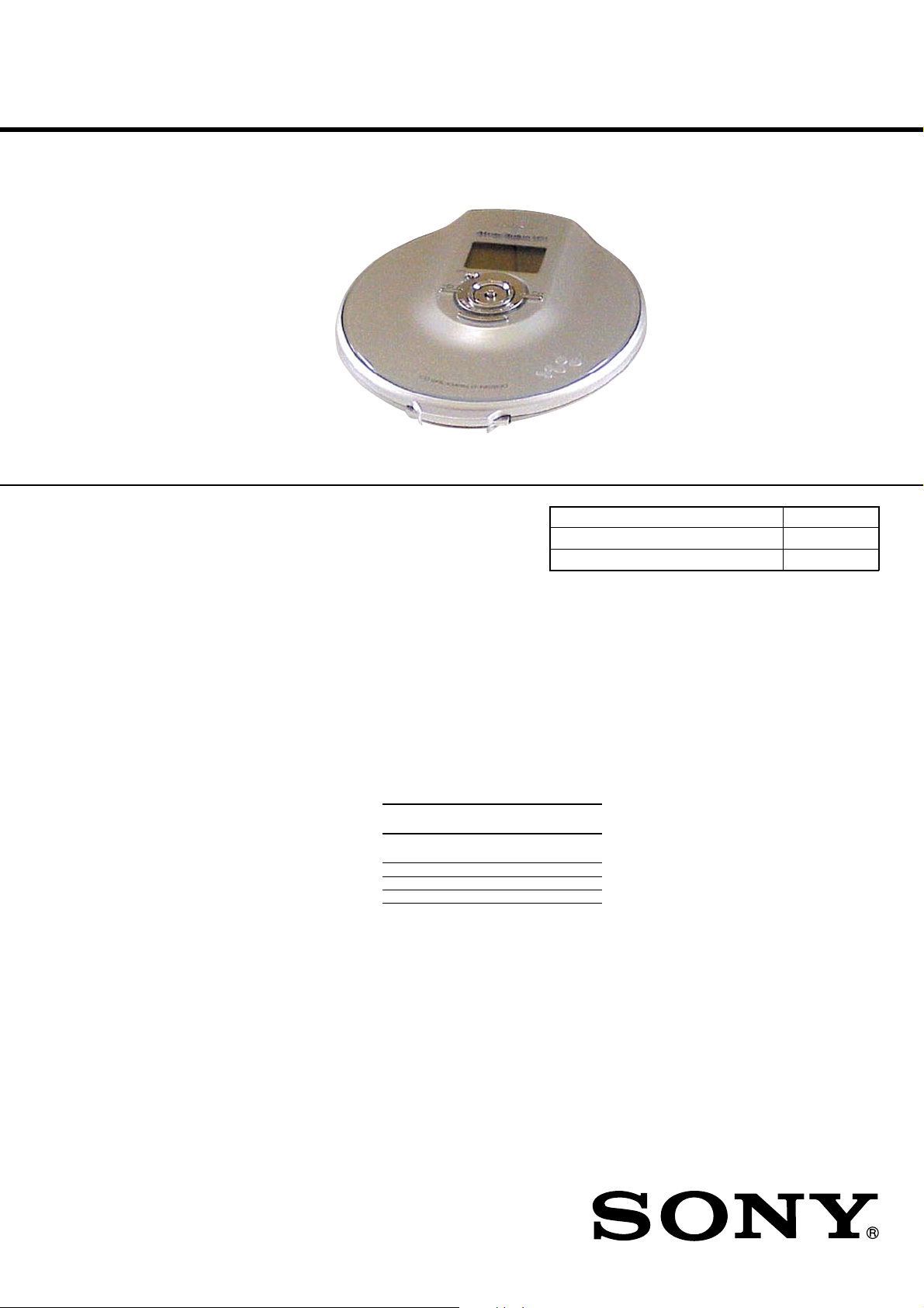
Photo: D-NE500
SPECIFICATIONS
US Model
Canadian Model
D-NE500/NE506CK
E Model
D-NE500
Model Name Using Similar Mechanism D-NE509
CD Mechanism Type CDM-3325ER2
Optical Pick-up Name DAX-25E
CD player
System
Compact disc digital audio system
Laser diode properties
Material: GaAlAs
Wav elength: λ = 770 - 800 nm
Emission duration: Continuous
Laser output: Less than 44.6 µW
(This output is the value measured at a distance
of 200 mm from the objective lens surface on
the optical pick-up block with 7 mm aperture.)
D-A conversion
1-bit quartz time-axis control
Frequency response
20 - 20 000 Hz dB (measured by JEITA)
Output (at 3 V input level)
Headphones (stereo minijack)
Approx. 5 mW + Approx. 5 mW at 16 Ω
+1
–2
General
Power requirements
• LR6 (size AA) battery: 1.5 V DC × 1
•AC power adaptor (DC IN 3 V jack):
120 V, 60 Hz
Battery life*1 (approx. hours)
When you use the CD player on a flat and stable
surface.
When LIGHT mode and SOUND mode are set to
“OFF.”
Playing time varies depending on how the CD
player is used.
US, CND model:
When using one Sony alkaline battery LR6
(SG) (produced in Japan)
G-PROTECTION
Audio CD 33 28
ATRAC CD
MP3 CD
*1 Measured value by the standard of JEITA
(Japan Electronics and Information Technology
Industries Association)
*2 Recorded at 48 kbps
*3 Recorded at 128 kbps
“G-PRO 1” “G-PRO 2”
2
*
3
*
60 60
45 45
Operating temperature
5°C - 35°C (41°F - 95°F)
Dimensions (w/h/d) (excluding projecting
parts and controls)
Approx. 129 × 27.5 × 140.1 mm
(5 1 ⁄8 × 1 1 ⁄8 × 5 5 ⁄8 in.)
Mass (excluding accessories)
Approx. 188 g (6.7 oz.)
Supplied accessories
AC power adaptor (1) (for except D-NE500:
US, except D-NE506CK: CND)
Remote control (1)
Rotary commander (1) (for D-NE506CK)
Car battery cord (1) (for D-NE506CK)
Car connecting pack (1) (for D-NE506CK)
Carrying case (1)
CD-ROM (SonicStage Ver. 2.0) (1)
User’s guide for SonicStage Ver. 2.0 (1)
Headphones (1) (for US model)
Earphones (1) (for other models)
US and foreign patents licensed from Dolby
Laboratories.
Design and specifications are subject to change
without notice.
•Abbreviation
CND : Canadian model
E92 : AC 120V area in E model
MX : Mexican model
9-877-555-03
2005F04-1
© 2005.06
PORTABLE CD PLAYER
Sony Corporation
Personal Audio Group
Published by Sony Engineering Corporation
1
D-NE500/NE506CK
Flexible Circuit Board Repairing
• Keep the temperature of the soldering iron around 270°C during
repairing.
• Do not touch the soldering iron on the same conductor of the
circuit board (within 3 times).
• Be careful not to apply force on the conductor when soldering
or unsoldering.
Notes on Chip Component Replacement
• Never reuse a disconnected chip component.
• Notice that the minus side of a tantalum capacitor may be
damaged by heat.
Notes on the power source
Disconnect all power sources when the CD player is not used for a
long time.
On AC power adaptor
• Use only the AC power adaptor supplied.
If your CD player is not supplied with the one, use the A C-E30HG
AC power adaptor. Do not use any other AC power adaptor. It
may cause a malfunction.
Polarity of the plug
z
UNLEADED SOLDER
Boards requiring use of unleaded solder are printed with the lead
free mark (LF) indicating the solder contains no lead.
(Caution: Some printed circuit boards may not come printed with
the lead free mark due to their particular size.)
: LEAD FREE MARK
Unleaded solder has the following characteristics.
• Unleaded solder melts at a temperature about 40°C higher than
ordinary solder.
Ordinary soldering irons can be used but the iron tip has to be
applied to the solder joint for a slightly longer time.
Soldering irons using a temperature regulator should be set to
about 350°C.
Caution: The printed pattern (copper foil) may peel away if the
heated tip is applied for too long, so be careful!
• Strong viscosity
Unleaded solder is more viscous (sticky, less prone to f low)
than ordinary solder so use caution not to let solder bridges
occur such as on IC pins, etc.
• Usable with ordinary solder
It is best to use only unleaded solder but unleaded solder may
also be added to ordinary solder.
• Do not touch the AC power adaptor with wet hands.
• Connect the A C po wer adaptor to an easily accessible AC outlet.
Should you notice an abnormality in the AC power adaptor,
disconnect it from the AC outlet immediately.
SAFETY-RELATED COMPONENT WARNING!!
COMPONENTS IDENTIFIED BY MARK 0 OR DOTTED LINE
WITH MARK 0 ON THE SCHEMATIC DIAGRAMS AND IN
THE PARTS LIST ARE CRITICAL TO SAFE OPERATION.
REPLACE THESE COMPONENTS WITH SONY P ARTS WHOSE
PART NUMBERS APPEAR AS SHOWN IN THIS MANUAL OR
IN SUPPLEMENTS PUBLISHED BY SONY.
2
ATTENTION AU COMPOSANT AYANT RAPPORT
À LA SÉCURITÉ!!
LES COMPOSANTS IDENTIFIÉS P AR UNE MARQUE 0 SUR LES
DIAGRAMMES SCHÉMATIQUES ET LA LISTE DES PIÈCES
SONT CRITIQUES POUR LA SÉCURITÉ DE FONCTIONNEMENT .
NE REMPLACER CES COMPOSANTS QUE PAR DES PIÈCES
SONY DONT LES NUMÉROS SONT DONNÉS DANS CE MANUEL
OU DANS LES SUPPLÉMENTS PUBLIÉS PAR SONY.

TABLE OF CONTENTS
1. SERVICE NOTE................................................................. 4
2. GENERAL
Locating the controls ............................................................... 5
3. DISASSEMBLY
3-1. Upper Lid Assy ................................................................... 7
3-2. Cabinet (Middle) Assy ........................................................ 7
3-3. Main Board, MD Assy ........................................................ 8
3-4. Sled Motor Assy (M602), Optical Pick-up (DAX-25E),
Turntable Motor Assy (M601)............................................. 8
4. ELECTRICAL ADJUSTMENTS
CD Section .............................................................................. 9
5. DIAGRAMS
5-1. IC Pin Descriptions ........................................................... 10
5-2. Note for Printed Wiring Boards
and Schematic Diagrams .................................................. 15
5-3. Waveforms......................................................................... 15
5-4. Block Diagram –CD Section–........................................... 16
5-5. Block Diagram –Power Supply Section–.......................... 17
5-6. Printed Wiring Board –Main Section– .............................. 18
5-7. Schematic Diagram –Main Section (1/2)– ......................... 20
5-8. Schematic Diagram –Main Section (2/2)– ......................... 21
5-9. Printed Wiring Board –Switch Section– ........................... 22
5-10. Schematic Diagram –Switch Section–............................... 23
5-11. IC Block Diagrams............................................................ 24
D-NE500/NE506CK
6. EXPLODED VIEWS
6-1. Upper Lid Section ............................................................. 25
6-2. Cabinet (Lower) Section ................................................... 26
6-3. CD Mechanism Deck Section (CDM-3325ER2) .............. 27
7. ELECTRICAL PARTS LIST......................................... 28
3
D-NE500/NE506CK
3
SECTION 1
SERVICE NOTE
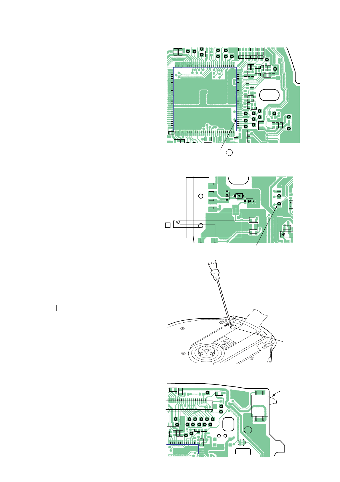
NOTES ON HANDLING THE OPTICAL PICK-UP BLOCK
OR BASE UNIT
The laser diode in the optical pick-up block may suffer electrostatic breakdown because of the potential difference generated by
the charged electrostatic load, etc. on clothing and the human body .
During repair, pay attention to electrostatic breakdown and also
use the procedure in the printed matter which is included in the
repair parts.
The flexible board is easily damaged and should be handled with
care.
Precautions for Checking Emission of Laser Diode
Laser light of the equipment is focused by the object lens in the
optical pick-up so that the light focuses on the reflection surface
of the disc. Therefore, be sure to keep your eyes more then 30 cm
apart from the object lens when you check the emission of laser
diode.
Before Replacing the Optical Pick-Up Block
Please be sure to check throughly the parameters as par the “Optical Pick-Up Block Checking Procedures” (Part No.: 9-960-027-
11) issued separately before replacing the optical pick-up block.
Note and specifications required to check are given below.
• FOK output : IC601 yg pin (or TP624 (FOK))
When checking FOK, remove the lead wire to disc motor.
• RF signal P-to-P value : 0.45 ± 0.1 Vp-p
• The repairing grating holder is impossible.
Laser Diode Checking Methods
During normal operation of the equipment, emission of the laser
diode is prohibited unless the upper lid is closed while turning ON
the S803. (push switch type)
The following two checking methods for the laser diode are
operable.
– MAIN BOARD (SIDE B) –
120
R641
1
30
R631
VDR603
31
TP644
C625
TP648 TP646
FB603
RP642
TP640
TP639
IC601
C623
FB606
C621
R628
TP636TP635
IC601 65 pin
– MAIN BOARD (SIDE A) –
J301
i
J301
TP633TP632
D306
TP631
90
61
R630
R611
R610
R606
R605
R618
C615
TP627TP623TP621
R612
R624R623
D101
C608
C603
R625
R603
C605
R613
R608
R103
R203
FB101
FB303
FB201
C614
C609
TP622TP626TP630
R602
R604
C604
R620
R616
C613
TP629
R609
TP625
FB301
C610
C611
TP610
R615
TP302
R614
R315
TP628
TP701
R314
TP624
C612
C311
VDR602
TP301
TP102
X601
VDR609
C617
C616
91
60
FB602
D305
TP624
• Method:
Emission of the laser diode is visually checked.
1. Open the upper lid.
2. With a disc not set, turn on the S803 with a screwdriv er having a
thin tip.
Note: Do not push the detection lever strongly , or it may be bent
or damaged.
3. Press the N X button.
4. Obser ving the objective lens, check that the laser diode emits
light.
When the laser diode does not emit light, automatic power
control circuit or optical pick-up is faulty.
In this operation, the objective lens will move up and down 5
times along with inward motion for the focus search.
– MAIN BOARD (SIDE B) –
TP831 TP827
TP829 TP825
TP830
TP832
R834 R832
R840
TP806
26
25
TP823
24
TP828
VDR802
VDR804
TP826
C812
TP835
R842
TP842
R827
R828
CN802
R829
R847
R303
TP846
TP833
TP834
TP822
TP824
SL806
S80
S803
S803
(OPEN/CLOSE)
4
SECTION 2
1
4
GENERAL
D-NE500/NE506CK
This section is extracted
from instruction manual.
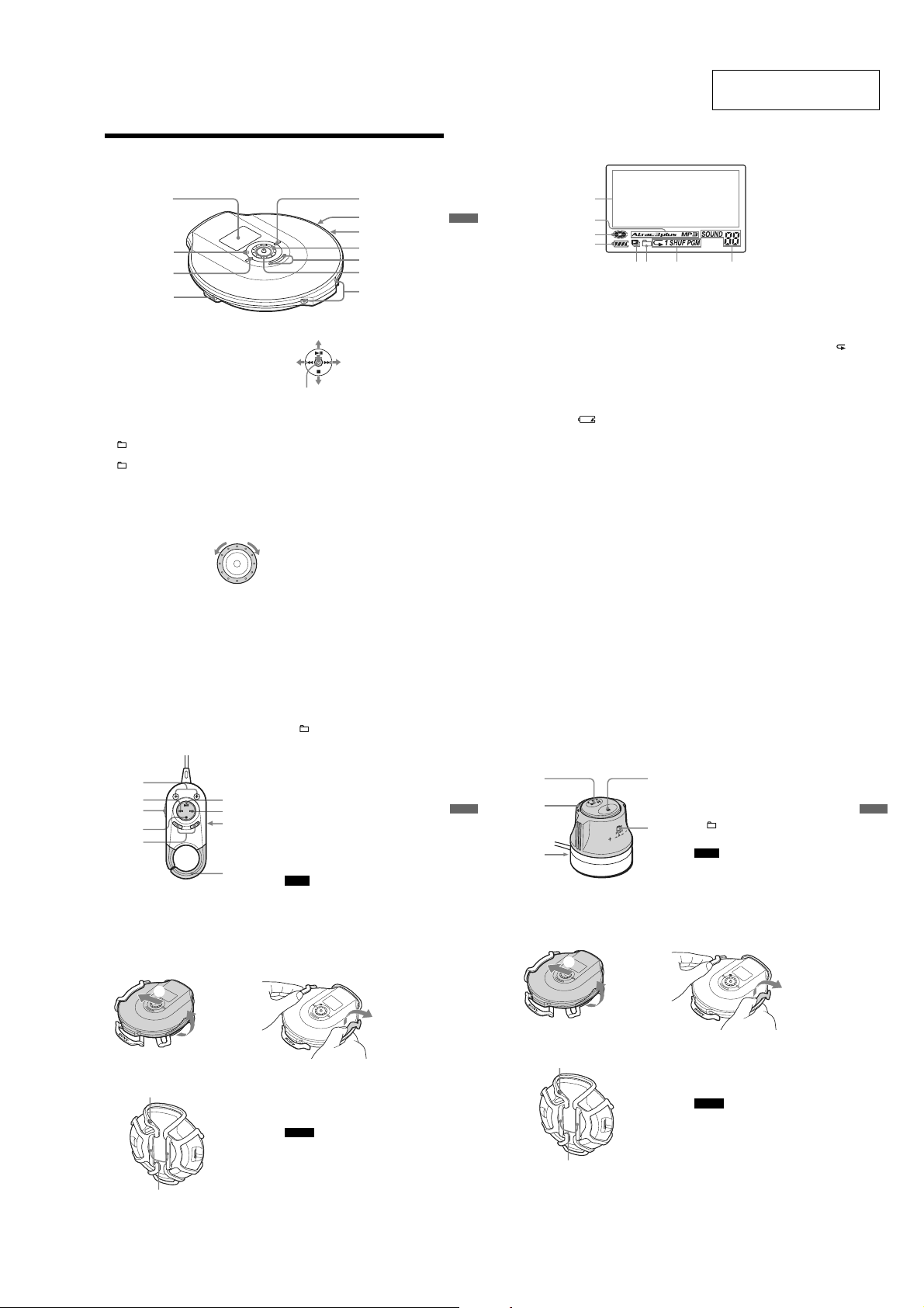
Locating the controls
CD player
For details, see the pages in parentheses.
2
3
4
1 Display (12, 16, 18, 19, 21 - 23, 33, 34)
2 OPR (operation) lamp (25, 26)
Color of the lamp changes according to
the type of music source being played.
Red: Audio CD, Green: ATRAC3plus/
ATRAC3 file, Orange: MP3 file
For some time after the CD is inserted,
the lamp lights up in red, orange and
green in turn.
This lamp also functions as the HOLD
lamp.
(group) – button (15, 21 - 23, 25, 33)
3
4 i (headphones) jack (14)
(group) + button (15, 21, 22)
5
6 HOLD switch (rear) (25)
Slide the switch in the direction of the
arrow to disable the buttons on the CD
player.
7 DC IN 3 V (external power input) jack
(14)
8 Jog dial (18 - 27, 33)
Use to select a f
mode, etc. The search
direction changes
according to the direction
in which the jog dial is turned.
9 VOL (volume) +
ile, play
*1/–
buttons (15)
5
6
7
8
9
q;
qa
q; 5-way control key
DISPLAY/
MENU
Push the control key toward u, .,
> or x with your finger on
DISPLAY/MENU.
qa OPEN switch (14, 31)
Squeeze the switch from both sides.
*1 The button has a tactile dot.
Automatic Music Sensor
*2
(15, 16, 18 - 27, 33)
u: play/pause
*2
.:AMS
/rewind
>:AMS/fast forward
x: stop
DISPLAY/MENU: Use to
select menu items and enter
the selection.
(Continued)
Getting started
Display
For details, see the pages in parentheses.
1
2
3
4
56 7 8
1 Character information display (16)
While playing an audio CD, disc name,
track name, etc. appear in 4 lines, if
recorded on the CD.
While playing an ATRAC CD/MP3 CD,
group name, file name, etc. appear in 4
lines, if recorded on the CD.
Menu items also appear in this display.
2 Atrac3plus/MP3 indication
3 Disc indication
Lights up while the CD player is playing.
4 Battery indication (31)
Roughly shows the remaining power of
the battery. If “
is depleted.
” flashes, the battery
5 Play list indication
For MP3 CD only
6 Group indication
For ATRAC CD/MP3 CD only
7 Play mode indication
Shows various play modes such as single
play, shuffle play and program play. “
shows repeat play.
8 SOUND indication
Shows the SOUND setting which has
been selected on the menu.
”
Remote control
For details, see the pages in parentheses.
1
2
3
4
6
7
8
5
9
1 ( group) –/+ buttons (15)
2 . (AMS/rewind) button (15)
3 HOLD switch (25)
Slide the switch in the direction of the
arrow to disable the buttons on the
remote control.
4 x (stop) button (15)
5 VOL (volume) +/– buttons (15)
6 u (play/pause) button (15)
7 > (AMS/fast forward) button (15)
8 Headphone jack (rear)
9 Hook
Use to hang the remote control on a
knapsack, etc.
Note
Use only the supplied remote control. You cannot
operate this CD player with the remote control
supplied with other CD players.
Using the carrying case
To attach the case To remove the case
1
2
You can pass your strap or belt through the case.
Strap hole
Notes
• The carrying case is not designed to protect the
CD player.
• When attaching and removing the case,
disconnect the AC power adaptor and the remote
control first.
Belt loop
11
Getting
started
12
• D-NE506CK
Rotary commander
For details, see the pages in parentheses.
1 u (play/pause) button (15)
1
2
5
3
Using the carrying case
To attach the case To remove the case
1
2
You can pass your strap or belt through the case.
Strap hole
Belt loop
2 .(AMS/search)•> (AMS/search)
control (15)
3 Jack for connecting a car connecting pack
(28)
4 x (stop) button (15)
( group) +/– control (15)
5
Push down and turn.
Note
The supplied rotary commander should be used
with this player only.
Notes
• The carrying case is not designed to protect the
CD player.
• When attaching and removing the case,
disconnect the AC po wer adaptor and the remote
control first.
Getting
started
13
13
5
D-NE500/NE506CK
SECTION 3
DISASSEMBLY
• The equipment can be removed using the following procedure.
SET
3-1. UPPER LID ASSY
(Page 7)
3-2. CABINET (MIDDLE) ASSY
(Page 7)
3-3. MAIN BOARD,
MD ASSY
(Page 8)
3-4. SLED MOTOR ASSY (M602),
OPTICAL PICK-UP (DAX-25E),
TURNTABLE MOTOR ASSY (M601)
(Page 8)
6
Note : Follow the disassembly procedure in the numerical order given.
1
screw
2
bracket (hinge R)
upper lid assy
spring (upper lid)
5
7
6
4
bracket (hinge L)
3
screw
s
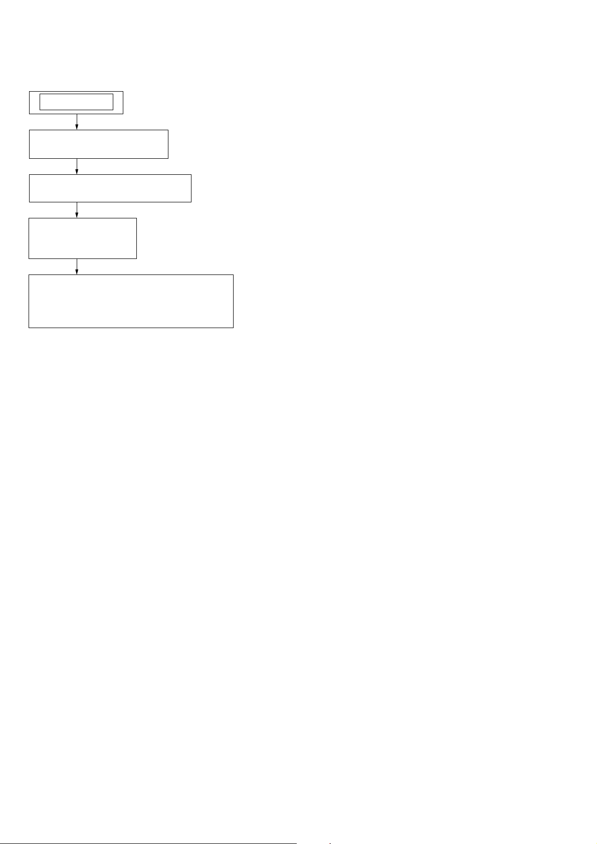
3-1. UPPER LID ASSY
D-NE500/NE506CK
3-2. CABINET (MIDDLE) ASSY
5
cabinet (middle) assy
two claws
3
screw
2
three
screws
4
1
three
screw
7
D-NE500/NE506CK
p
3-3. MAIN BOARD, MD ASSY
Note: When installing, fit the knob (HOLD) and S802.
1
CN602
2
CN603
3
CN602
4
5
MD ASSY
8
CN802
7
MAIN board
6
cabinet (lower) assy
S802
knob (hold)
claw
3-4. SLED MOTOR ASSY (M602), OPTICAL PICK-UP (DAX-25E), TURNTABLE MOTOR ASSY (M601)
1
three screws
(B1.7x4)
7
standard shaft
2
gear cover
8
three screws
(B1.7x4)
9
turntable motor assy
(M902)
sled motor assy
4
(M901)
3
5
Chassis
6
optical pick-u
(DAX-25E)
8
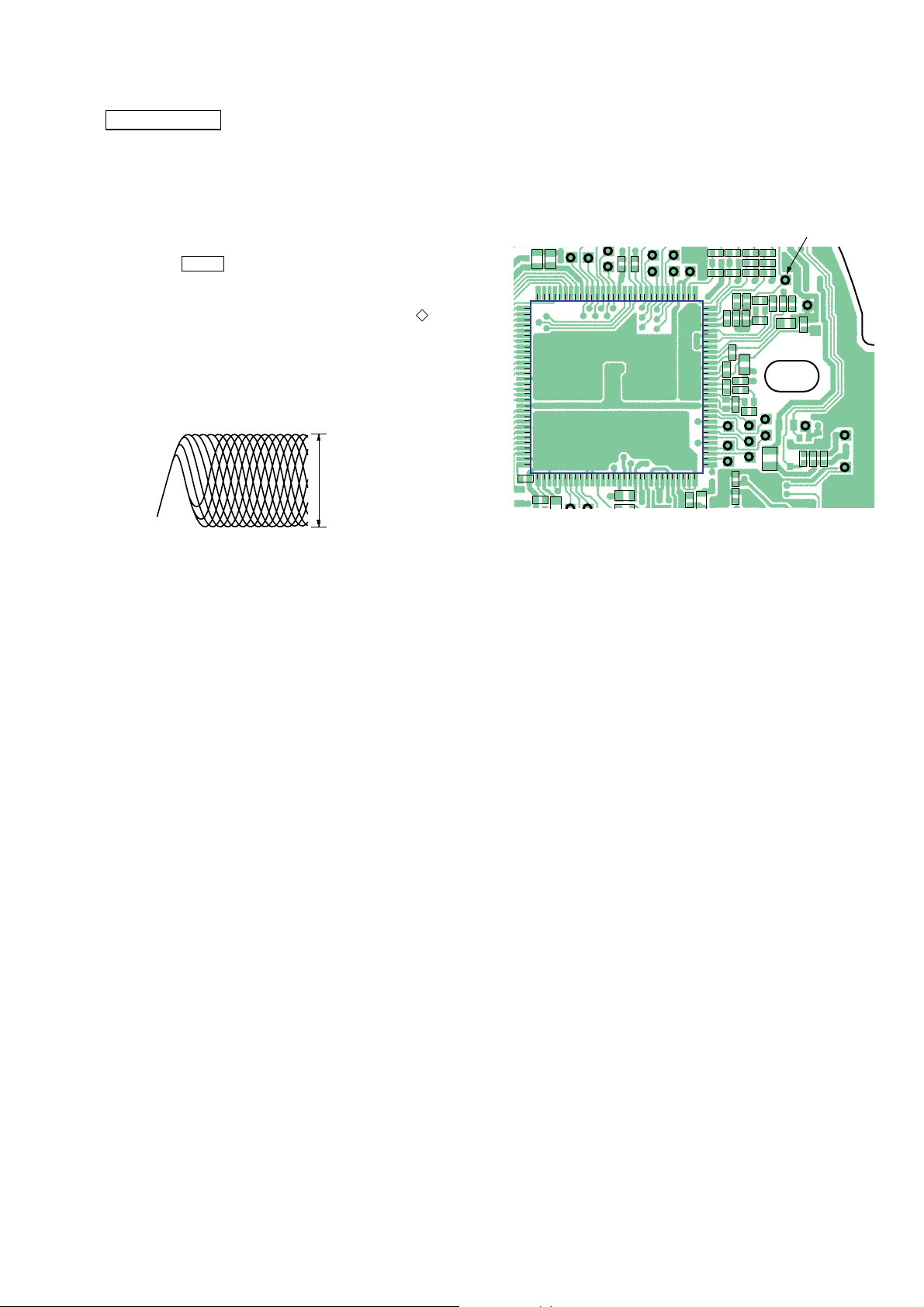
ELECTRICAL ADJUSTMENTS
CD SECTION
CD section adjustments are done automatically in this set.
In case of operation check, confirm that focus bias.
D-NE500/NE506CK
SECTION 4
FOCUS BIAS CHECK
1. Connect the oscilloscope between TP610 (RF) and GND on
main board.
2. Insert the disc (YEDS-18). (Part No. : 3-702-101-01)
3. Press the N X button.
4. Confirm that the oscilloscope waveform is as shown in the
figure below. (eye pattern)
A good eye pattern means that the diamond shape ( ) in the
center of the waveform can be clearly distinguished.
• RF signal reference waveform (eye pattern)
VOLT/DIV : 20 mV (10 : 1 probe in use)
TIME/DIV : 500 nS
RF level :
0.45
±
0.1 Vp-p
When observing the eye pattern, set the oscilloscope for AC range
and raise vertical sensitivity.
Test Point:
– MAIN BOARD (SIDE B) –
120
R641
1
30
R631
VDR603
31
TP644
C625
TP648 TP646
FB603
RP642
TP640
TP639
IC601
C623
FB606
C621
R628
TP636TP635
TP633TP632
TP631
90
61
R630
TP610
R611
R610
R606
R605
R618
C615
TP627TP623TP621
R612
R624R623
R625
C608
C603
R603
C605
R613
R103
R203
C614
R608
TP622TP626TP630
R602
R604
C609
C604
R620
R616
C613
TP629
R609
TP625
FB301
C610
C611
TP610
R615
TP302
R614
R315
TP701
R314
C311
TP301
TP102
C616
91
60
FB602
9
D-NE500/NE506CK
SECTION 5
DIAGRAMS
5-1. IC PIN DESCRIPTIONS
• IC601 CXD3039AR (RF AMP, DIGITAL SIGNAL PROCESSOR, DIGITAL SERVO PROCESSOR, D-RAM CONTROLLER)
(MAIN BOARD (1/2))
Pin No. Pin Name I/O Pin Description
1 XRAS O Row address strobe signal output to the D-RAM
2 XWE O Data input enable signal output to the D-RAM
3 to 6 D1, D0, D3, D2 I/O Two-way data bus with the D-RAM
7 DCLK O Not used
8 DCKE O Not used
9 XCAS O Column address strobe signal output to the D-RAM
10 WFCK/DQM O WFCK signal output terminal Not used
11 to 13 A9 to A7 O Address signal output to the D-RAM
14 DVSS — Ground terminal (for D-RAM interface)
15 to 17 A6 to A4 O Address signal output to the D-RAM
18 XRDE I D-RAM read enable signal input terminal
19 VDD0 — Power supply terminal (digital system)
20 CLOK I Serial data transfer clock input from the system controller
21 SDTO I Serial data input from the system controller
22 SENS O Serial data output to the system controller
23 XLAT I Serial data latch pulse signal input from the system controller
24 XSOE I Serial data output enable signal input from the system controller
25 SYSM I Analog muting on/off control signal input “H”: muting on
26 WDCK O GRSCOR signal output to the system controller Not used
27 SCOR O Subcode sync (S0+S1) detection signal output to the system controller
28 XRST I Reset signal input from the system controller “L”: reset
29 PWMI I Spindle motor external control signal input terminal Not used
30 XQOK I Subcode Q OK signal input terminal Not used
31 XWRE I D-RAM write enable signal input terminal Not used
32 R8M O System clock output to the system controller
33 VSS0 — Ground terminal (digital system)
34 SQCK I SQSO readout clock input terminal Not used
35 SCLK I SENS serial data read clock input terminal Not used
36 SQSO O CD text data output terminal Not used
37 XEMP O D-RAM read prohibition signal output terminal Not used
38 XWIH O D-RAM write prohibition signal output terminal Not used
39 SBSO O Subcode P to W serial data output terminal Not used
40 EXCK O SQSO readout clock output terminal Not used
41 XTSL I Input terminal for the system clock frequency setting Not used
42 HVSS — Ground terminal (for headphone)
43 HPL O PDM signal output for L-ch headphone to the headphone amplifier Not used
44 HPR O PDM signal output for R-ch headphone to the headphone amplifier Not used
45 HPVDD — Power supply terminal (for headphone)
46 XVDD — Power supply terminal (for master clock)
47 XTAI I System clock input terminal (16.9344 MHz)
48 XTAO O System clock output terminal (16.9344 MHz)
49 XVSS — Ground terminal (for master clock)
50 AVDD1 — Power supply terminal (analog system)
51 AOUT1 O L-ch analog audio signal output
52 VREFL O L-ch reference voltage output terminal
53, 54 AVSS1, AVSS2 — Ground terminal (analog system)
55 VREFR O R-ch reference voltage output terminal
56 AOUT2 O R-ch analog audio signal output
10

D-NE500/NE506CK
Pin No. Pin Name I/O Pin Description
57 AVDD2 — Power supply terminal (analog system)
58 TES1 I Input terminal for the test (normally: fixed at “L”)
59 TEST I Input terminal for the test (normally: fixed at “L”)
60 VSS1 — Ground terminal (digital system)
61 LRMU O
62 DOUT O Digital audio signal output Not used
63 ATSK I/O Input/output terminal for anti-shock Not used
64 DFCT I/O Defect signal input/output terminal Not used
65 FOK O Focus OK signal output to the system controller “L”: NG, “H”: OK
66 MIRR I/O Defect signal input/output terminal Not used
67 COUT I/O Numbers of track counted signal input/output terminal Not used
68 C2PO O C2PO signal output terminal Not used
69 GFS O GFS signal output terminal
70 XUGF O XUGF signal output terminal Not used
71 XPCK O XPCK signal output terminal Not used
72 VDD1 — Power supply terminal (digital system)
73 PCO O Charge pump output for master PLL
74 FILI I Filter input for master PLL
75 FILO O Filter output for master PLL
76 CLTV I VCO1 control voltage input terminal for multiplier
77 VCTL I VCO2 control voltage input terminal for broad-band EFM PLL
78 VPCO O Charge pump output terminal for broad-band EFM PLL
79 AVSS3 — Ground terminal (analog system)
80 ASY_O O EFM full-swing output terminal
81 ASY_I I Asymmetry comparator voltage input terminal
82 BIAS I Asymmetry circuit constant current input terminal
83 AVDD3 — Power supply terminal (analog system)
84 RFAC I EFM signal input from the optical pick-up
85 AVDD0 — Power supply terminal (analog system)
86 IGEN I Stabilized current input for operational amplifiers
87 AVSS0 — Ground terminal (analog system)
88 RFDC I RF signal input from the optical pick-up
89 E I E signal input from the optical pick-up
90 F I F signal input from the optical pick-up
91 B I B signal input from the optical pick-up
92 A I A signal input from the optical pick-up
93 VC I Middle point voltage input terminal Not used
94 VSS2 — Ground terminal (digital system)
95 FRDR O Focus servo drive signal (–) output to the IC401
96 FFDR O Focus servo drive signal (+) output to the IC401
97 TRDR O Tracking servo drive signal (–) output to the IC401
98 TFDR O Tracking servo drive signal (+) output to the IC401
99 SRDR O Sled servo drive signal (–) output to the IC401
100 SFDR O Sled servo drive signal (+) output to the IC401
101 SSTP I Disc inner position detection signal input terminal Not used
102 MDS O Spindle motor drive signal output to the spindle motor driver
103 MDP O Spindle motor servo control signal output to the spindle motor driver
104 C176 O 176.4 kHz clock output to the power control and spindle motor driver
105 VDD2 — Power supply terminal (digital system)
106 LRCK_O O L/R sampling clock (44.1 kHz) output terminal
Muting on/off control signal output to the audio line and the headphone amplifier
“H”: muting on
11
 Loading...