

Page 1
DPP-MS300
SERVICE MANUAL
SPECIFICATIONS
US Model
Canadian Model
9-928-127-11
– Continued on next page –
DIGITAL PHOTO PRINTER
Page 2
DPP-MS300
5-8. PRINTED WIRING BOARD – VS-40 Board –
VS-40 BOARD
(SIDE A)
A
B
C
D
K
A
K/A
VS-40 BOARD
(SIDE B)
A
K
K
8
1
A
5-9. SCHEMATIC DIAGRAM – VS-40 Board –
J1802
OUTPUT
VI-40 BOARD
A
CN101
(Page 5-17)
K
K
J1801
VIDEO
INPUT
(Page 5-19)
E
F
05
• Semiconductor
Location
(Side A)
Ref. No. Location
D1811 E-2
D1812 A-1
1-674-243-
1 2
CJ1801
S VIDEO
K
A
K
K
K/A
A
K
A
K
(ON:PLUG IN)
4
2
1
3
11
(11)
05
1-674-243-
11
(11)
• Semiconductor
Location
(Side B)
Ref. No. Location
D1801 E-2
D1802 F-2
D1803 E-2
D1804 C-1
D1805 B-1
5-15
5-16
Page 3
5-11. SCHEMATIC DIAGRAM – VI-40 Board – • See page 5-52 for Waveforms. • See page 5-55 for IC Block Diagrams.
(Page
5-16)
DPP-MS300
(Page
5-25)
5-19
5-20
5-21
Page 4
5-13. SCHEMATIC DIAGRAM – DK-40 Board (1/3) – • See page 5-53 for Waveforms.
DPP-MS300
(Page 5-30)
(Page 5-28)
(Page 5-31)
(Page 5-32)
(Page 5-30)
(Page 5-30)
(Page
5-21)
5-25
5-26
5-27
Page 5
DPP-MS300
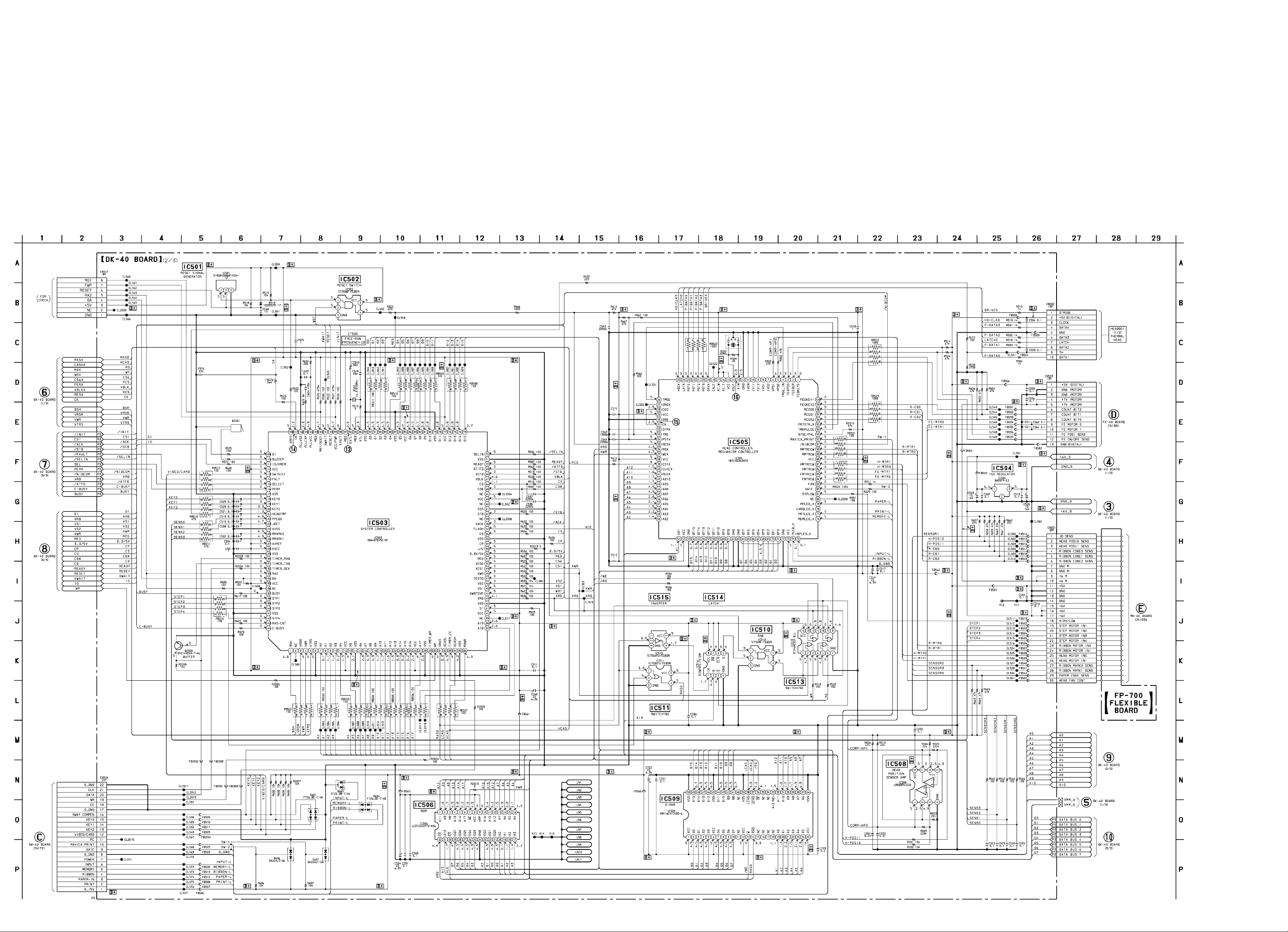
5-14. SCHEMATIC DIAGRAM – DK-40 Board (2/3) – • See page 5-53 for Waveforms.
(Page 5-27)
(Page 5-32)
(Page 5-32)
(Page 5-41)
(Page 5-25)
(Page 5-25)
(Page 5-49)
(Page
5-46)
5-28
5-29
(Page 5-32)
(Page 5-27)
(Page 5-32)
5-30
Page 6

5-15. SCHEMATIC DIAGRAM – DK-40 Board (3/3) – • See page 5-56 for IC Block Diagrams.
(Page
5-35)
DPP-MS300
(Page 5-28)
(Page
5-35)
(Page
5-25)
(Page 5-25)
(Page 5-30)
(Page 5-30)
(Page
5-41)
5-31
(Page 5-28)
5-32
Page 7

5-17. SCHEMATIC DIAGRAM – MP-40 Board – • See page 5-54 for Waveforms. • See page 5-57 for IC Block Diagrams.
(Page
5-31)
DPP-MS300
(Page
5-31)
5-35
5-36
5-37
Page 8

5-19. SCHEMATIC DIAGRAM – FE-40/JK-40 Boards –
DPP-MS300
(Page 5-31)
(Page 5-30)
5-41
5-42
Page 9

5-21. SCHEMATIC DIAGRAM – SW-40 Board – • See page 5-58 for IC Block Diagram.
DPP-MS300
(Page 5-28)
5-45 5-46
Page 10

5-23. SCHEMATIC DIAGRAM – HP-40/JD-40/MD-40/RD-40 Boards – • See page 5-57 for IC Block Diagrams.
(Page
5-30)
DPP-MS300
5-49
5-50
The components identified by mark ! or dotted
line with mark ! are critical for safety.
Replace only with part number specified.
5-51
Les composants identifiés par une marque ! sont
critiques pour la sécurité. Ne les remplacer que
par une piéce portant le numéro spécifié.
Page 11

• Waveforms
4.9 Vp-p
14.31818 MHz
1.4 Vp-p
20 MHz
5.8 Vp-p
99.5 ns
– VI-40 Board –
– DK-40 Board –
– MP-40 Board –
1 IC105 #ª (ACO), IC101 7
H
2 IC105 #¡ (AYO), IC102 7
H
3 IC105 @∞ (ADIN)
0.7 Vp-p
1Vp-p
1.5 Vp-p
6 IC108 !ª (B-Y)
H
7 IC108 !• (SC OUT)
3.58 MHz
8 IC108 !º (VCXO)
0.9 Vp-p
0.7 Vp-p
1 Vp-p
!¡ IC103 !º (SYNC IN)
H
!™ IC103 6 (XO IN)
3.58 MHz
5 Vp-p
1 Vp-p
1 IC401 #¶ (YMCK)
7.8 Vp-p
69 ns
2 IC401 @¶ (AFH) 7 IC407 ^¢ (YIN)
5.2 Vp-p
64
µ
s
3 IC401 @£ (BFP)
4.8 Vp-p
6 IC407 &£ (UIN)
8 IC407 $£ (V_OUT)
!¡ IC407 @º (SYCX)
1.6 Vp-p
H
!™ IC407 !ª (SC)
1.5 Vp-p
H
!£ IC503 (§ (EXTL)
0.7 Vp-p
H
3.58 MHz
5.1 Vp-p
6.8Vp-p
!§ IC505 !£ (XIN)
1.4 Vp-p
20 MHz
1 IC1501 @™ (XIN) (MEMORY STICK insert)
2 IC1501 ^º (P CLK), IC1502 %¡ (EXTAL)
(MEMORY STICK insert)
6.6 Vp-p
99.5 ns
3 IC1501 ^¡ (EXTCLK1), IC1502 $§
(EXTAL0), IC1503 @• (P CLK)
(MEMORY STICK insert)
H
4 IC108 @∞ (VIDEO)
5 IC108 @º (R-Y)
H
14.318 MHz
9 IC108 5 (C IN)
0.5 Vp-p
H
0 IC103 @º (V OUT)
1.1 Vp-p
H
H
0.4 Vp-p
2 Vp-p
4 IC407 `⁄⁄‹ (ICKI)
5 IC407 *™ (VIN)
69 ns
64
H
µ
s
9 IC407 #§ (U_OUT)
7.2 Vp-p
!º IC407 @ª (Y_OUT)
1 Vp-p
H
!¢ IC503 `⁄‚‡ (CK)
1 Vp-p
H
35 ns
!∞ IC505 #¡ (CK)
1.2 Vp-p
H
50 ns
6.2 Vp-p
7.4 Vp-p
5-52
5-53
5-54
Page 12

• IC Block Diagrams
– VI-40 Board –
IC101, 102 MM1113XFBE
IN1
SW1
IN2
SW2
1
2
3
4
SW
BIAS
IC103 CXA1229AM-T6
13
I REF
REGULATOR
14
V REF
OUT
Y IN
VCC2
C VIDEO
OUT
B OUT
G OUT
R OUT
GND2
15
Y
16
17
Y/C
MIX
18
19
VIDEO
OUT
20
B
21
OUT
G
22
OUT
23
OUT
MATRIX
R
CHROMA OUT
CHROMA IN
SW
+
R-Y
MODULATOR
SYNC
SLICE
BUFFER
B-Y
MODULATOR
8
GND
OUT
7
6
VCC
IN3
5
SYNC
OUT
BUFFER
PULSE
GENERATOR
PHASE
SHIFTER
X'TAL
OSC
CLAMP
CLAMP
CLAMP
12
11
10
9
8
7
6
5
4
3
2
124
C SYNC IN
AUDIO OUT
AUDIO IN
NTSC/PAL
XO IN
XO OUT
Y IN
B-Y IN
R-Y IN
GND1
VCC1
C SYNC OUT
IN
IC105 CXD2023Q
C3C4C5C6C7C8C9CAXYOEY1Y2
63 62 61 60 59 58 57 56 55 54 53 52 51 50 49 48 47 46 45 43 42 41
64 44
65
C2
66
C1
67
XCOE
68
APON
69
TEST
70
TEST
TST
71
DV
72
SS
73
DV
DD
74
TEST
75
TEST
76
TEST
77
TEST
78
TEST
79
BPF
80
TEST
1
V182V173V164V155V146V137V128V11
ADAPTIVE
FILTER
OPARATION
1HDL
1HDL
DVDDDVSSY3Y4Y5Y6Y7Y8Y9YACVSSCIRF
DAC
LOGIC
OPARATION
BPF
BPF
BPF
ADC
9
10
11
12
13
14
15
16
ADCO
INSL
OCLK
SS
DD
DV
DV
CLKO
MCK
17
ADCK
CLPI
DL
18
XCPON
19
+
20
ADVS
ICP
21
CRV
DAC
22RB23GR24
CVRF
40
39
38
37
36
35
34
33
32
31
30
29
28
27
26
25
AAVS
5-55
CVG
ACO
XACO
CV
VB
YV
YIRF
YVRF
YVG
AYO
XAYO
YV
ADVD
RT
AAVD
ADIN
DD
SS
DD
Page 13

IC108 M5127FP-70AD
SYNCO
SLC
FBC
VIDEO
HD
BLK
23 21 20 19 18 1722
24
KFC
KILF
R-Y OUT
B-Y OUT
R-Y IN
SC
NTSC/PAL
151628 27 26 25
VCC
SYNC
SEPARATOR
BURST GATE
PULSE
1 2 3 4 5 6
BGP
PGW
COMP
COMP
2nd
AMPLIFIER
C OUT
C CNT
– DK-40 Board –
IC701 HD74LS244FPEL
ID KILLER
DETECTOR
1st
AMPLIFIER
C IN
ID PULSE
BYPC
BURST
GATE
ACC
DETECTOR
7
ACCK
R-Y
DECODER
90°
270°
TINTO
REFERENCE
VOLTAGE
8 9 10 11 12 13 14
REFV
B-Y
DECODER
NTSC
PAL
APC
DETECTOR
APC
90°
90°
1/4
4FSC
VCXO
180°
VCXO
TIN
COMP
VCXI
GND
IC702 HD74LS374FP-EL
B-Y IN
2A2
1Y3
2A3
1Y2
2A4
1Y1
2G
Vcc
20 19 18 17 16 15 14 13 12 11
1 2 3 4 5 6 7 8 9 10
1G
1A1
2Y4
1A2
2Y3
1A3
2Y2
1A4
IC703 SN74HC74ANSR
14
13 12 11 10 9 8
VCC
D
1 2 3 4 5 6 7
PR
Q
D
CK
Q
CLR
PR
Q
Q
CK
CLR
GND
1Y4
2Y1
GND 2A1
VSS
20
OC
1
2
1Q
3
1D
4
2D
2Q
5
6
3Q
3D
7
4D
8
4Q
9
10
Q
EN
CK
CK
EN
EN
CK
CK
EN
EN
D
D
Q
Q
D
D
Q
CK
CK
EN
EN
CK
CK
EN
VDD
19
8Q
Q
D
18
8D
7D
17
D
Q
16
7Q
6Q
15
Q
D
6D
14
13
5D
D
Q
5Q
12
CK
11
5-56
Page 14

– MP-40 Board –
IC1531 SN74LVCC4245APWR
VCCA
1
T/R
2
IC1532 – 1534 74VHC244MTCX
IC1535 74VHCT244MTCX
VCCB
24
VCCB
23
Vcc
20 19 18 17 16 15 14 13 12 11
1Y1
2G
2A4
1Y2
2A3
1Y3
2A2
1Y4
AO
3
A1
4
5
A2
A3
6
A4
7
8
A5
A6
9
A7
10
GND
11
GND
12
– MD-40 Board –
IC1900 LB1644
VZ1
OE
22
BO
21
B1
20
B2
19
B3
18
B4
17
B5
16
15
B6
14
B7
GND
13
IN1
OUT1
14 131516
1 2 3 4 5 6 7 8 9 10
1G
1A1
2Y4
1A2
2Y3
1A3
2Y2
1A4
2Y1
GND
GND
12
OUT4
11
IN4
10
CC2
V
9
GND 2A1
PRE
DRIVER
TSD
INPUT LOGIC BLOCK INPUT LOGIC BLOCK
1
CC1
V
23
IN2
OUT2
4
GND
5
GND
PRE
DRIVER
6
OUT3
7
IN3
8
Z2
V
5-57
Page 15

IC1901 STA506A IC1902 LM339NS-E20
1
2
SWITCH
3
4
SWITCH
5
6
SWITCH
7
8
SWITCH
9
10
– SW-40 Board –
IC1700 RTC-4543SBB-L2
NC
1
2
NC
3
NC
4
NC
CONTROL CIRCUIT
VOLTAGE
DETECT
I/O CONTROLLER
SHIFT REGISTER
18
17
16
15
14
13
1 OUT
2 OUT
VCC
2 IN–
2 IN+
1 IN–
1 IN+
NC
NC
NC
NC
VCC
NC
1
2
3
4
5
6
7
14
3 OUT
13
4 OUT
2
GND
11
4 IN+
10
4 IN–
9
3 IN+
8
3 IN–
FOE
FSEL
GND
WR
12
5
CLOCK AND CALENDER
6
DEVIDER
7
8
CE
9
OSC
32.768kHz
OUT PUT
CONTROLLER
CLK
11
DATA
FOUT
10
5-58
 Loading...