

Page 1
D-FS601
SERVICE MANUAL
Ver 1.0 2002. 07
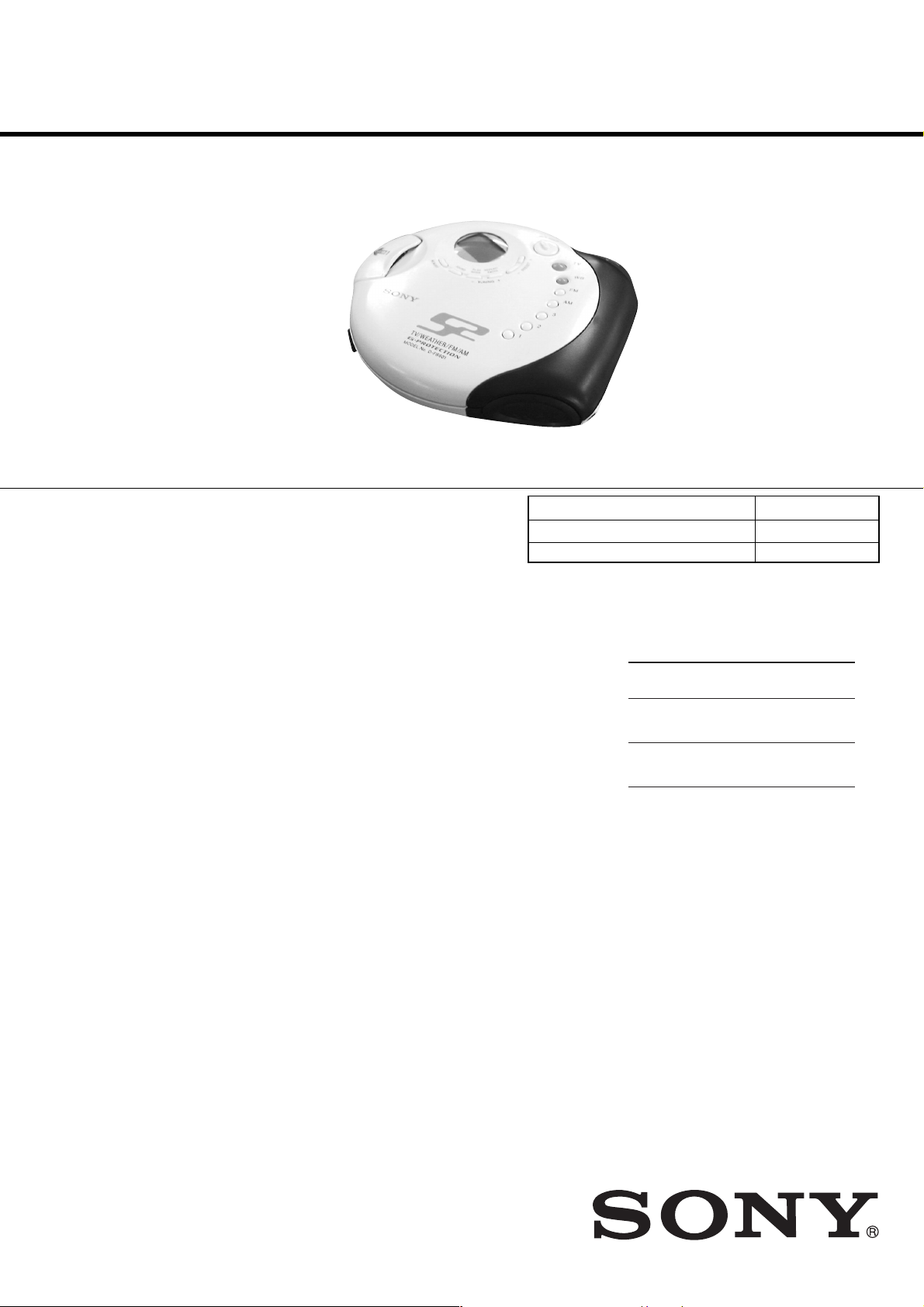
Photo : US model
SPECIFICATIONS
TV: 2 - 13 ch
WB (weather band): 1 - 7 ch
FM: 87.5 - 108.0 MHz
AM: 530 - 1 710 kHz
FM: 87.5 - 108.0 MHz
AM: 531 - 1 710 kHz
FM: 87.5 - 108.0 MHz
AM: 530 - 1 710 kHz
antenna
2.4 V DC
120 V, 60 Hz
CD player
System
Compact disc digital audio system
Laser diode properties
Material: GaAlAs
Wav elength: λ = 780 nm
Emission duration: Continuous
Laser output: Less than 44.6 µW
(This output is the value measured at a distance
of 200 mm from the objective lens surface on
the optical pick-up block with 7 mm aperture.)
D-A conversion
1-bit quartz time-axis control
Frequency response
40 - 20 000 Hz
307)
Output (at 4.5 V input level)
Headphones (stereo minijack)
Approx. 5 mW + Approx. 5 mW at 16 Ω
Radio
Frequency range (STEP switch)
•US model
9 kHz step:
TV: 2 - 13 ch
WB (weather band): 1 - 7 ch
FM: 87.5 - 108.0 MHz
AM: 531 - 1 710 kHz
0
dB (measured by JEITA CP-
–4.5
10 kHz step:
•Canadian model
9 kHz step:
10 kHz step:
Antenna
*(TV/WB/)FM:Headphones/earphones cord
AM: Built-in ferrite bar antenna
*US model only
General
Power requirements
For the area code of the model you
purchased, check the upper left side of the
bar code on the package.
• Sony NH-WM2AA rechargeable batteries:
•Two LR6 (size AA) batteries: 3 V DC
•AC power adaptor (DC IN 4.5 V jack)
US Model
Canadian Model
Model Name Using Similar Mechanism D-SJ301
CD Mechanism Type CDM-3125ER
Optical Pick-up Type DAX-25E
Battery life* (approx. hours)
(When you use the CD player on a flat and stable
surface.)
Playing time varies depending on how the CD
player is used.
When using G-PROTECTION RADIO
NH-WM2AA 32 35 40
(charged for
about 4 hours**)
Two Sony alkaline 46 50 70
batteries LR6 (SG)
(produced in Japan)
*Measured value by the standard of JEITA (Japan
Electronics and Information Technology
Industries Association).
** Charging time varies depending on how the
rechargeable battery is used.
Operating temperature
5°C - 35°C (41°F - 95°F)
Dimensions (w/h/d) (including
projecting parts and controls)
Approx. 133.9 × 38.1 × 147.5 mm
3
⁄8× 1 1⁄2× 57⁄8 in.)
(5
Mass (excluding accessories)
Approx. 331 g (11.7 oz.)
12 on
— Continued on next page —
9-874-078-01
2002G1600-1
© 2002.07
TV/WB/FM/AM PORTABLE CD PLAYER
US model
FM/AM PORTABLE CD PLAYER
Canadian model
Sony Corporation
Personal Audio Company
Published by Sony Engineering Corporation
Page 2
D-FS601
Supplied accessories
For the area code of the location in which you
purchased the CD player, check the upper left side
of the bar code on the package.
AC power adaptor (1)
Headphones/earphones (1)
Hand strap (1)
For US customers
The AC power adaptor supplied is not intended to
be serviced. Should the AC power adaptor cease to
function in its intended manner, during the warranty
period, the adaptor should be returned to your
nearest Sony Service Center or Sony Authorized
Repair Center for replacement, or after warranty
period, it should be discarded.
Design and specifications are subject to change
without notice.
Unleaded solder
Boards requiring use of unleaded solder are printed with the leadfree mark (LF) indicating the solder contains no lead.
(Caution: Some printed circuit boards may not come printed with
the lead free mark due to their particular size.)
: LEAD FREE MARK
Unleaded solder has the following characteristics.
• Unleaded solder melts at a temperature about 40°C higher than
ordinary solder.
Ordinary soldering irons can be used but the iron tip has to be
applied to the solder joint for a slightly longer time.
Soldering irons using a temperature regulator should be set to
about 350°C.
Caution: The printed pattern (copper foil) may peel away if the
heated tip is applied for too long, so be careful!
• Strong viscosity
Unleaded solder is more viscous (sticky, less prone to flow) than
ordinary solder so use caution not to let solder bridges occur such
as on IC pins, etc.
• Usable with ordinary solder
It is best to use only unleaded solder but unleaded solder may
also be added to ordinary solder.
DANGER
Invisible laser radiation when open and interlock failed or defeated.
Avoid direct exposure to beam.
CAUTION
Use of controls or adjustments or performance of procedures other
than those specified herein may result in hazardous radiation
exposure.
Laser component in this product is capable of emitting
radiation exceeding the limit for Class 1.
This Compact Disc player is
classified as a CLASS 1 LASER
product.
The CLASS 1 LASER
PRODUCT label is located on
the rear exterior.
Flexible Circuit Board Repairing
•Keep the temperature of the soldering iron around 270°C during
repairing.
• Do not touch the soldering iron on the same conductor of the
circuit board (within 3 times).
• Be careful not to apply force on the conductor when soldering or
unsoldering.
Notes on chip component replacement
•Never reuse a disconnected chip component.
• Notice that the minus side of a tantalum capacitor may be damaged by heat.
On AC power adaptor
• Use only the AC power adaptor supplied or
recommended in “Accessories (supplied/
optional).” Do not use any other AC power
adaptor. It may cause a malfunction.
Polarity of the plug
•When disconnecting the AC power adaptor
from the AC outlet, grasp the adaptor
itself. Do not pull it by the cord.
• Do not touch the AC power adaptor with
wet hands.
SAFETY-RELATED COMPONENT WARNING!!
COMPONENTS IDENTIFIED BY MARK 0 OR DOTTED LINE WITH
MARK 0 ON THE SCHEMATIC DIAGRAMS AND IN THE PARTS
LIST ARE CRITICAL TO SAFE OPERATION. REPLACE THESE
COMPONENTS WITH SONY PARTS WHOSE PART NUMBERS
APPEAR AS SHOWN IN THIS MANUAL OR IN SUPPLEMENTS
PUBLISHED BY SONY.
ATTENTION AU COMPOSANT AYANT RAPPORT
LES COMPOSANTS IDENTIFÉS PAR UNE MARQUE 0 SUR LES
DIAGRAMMES SCHÉMATIQUES ET LA LISTE DES PIÈCES SONT
CRITIQUES POUR LA SÉCURITÉ DE FONCTIONNEMENT. NE
REMPLACER CES COMPOSANTS QUE PAR DES PIÈSES SONY
DONT LES NUMÉROS SONT DONNÉS DANS CE MANUEL OU
DANS LES SUPPÉMENTS PUBLIÉS PAR SONY.
À LA SÉCURITÉ!
2
Page 3
SECTION 1
SERVICING NOTES
D-FS601
TABLE OF CONTENTS
1. SERVICING NOTES ······················································· 3
2. GENERAL ·········································································· 4
3. DISASSEMBLY ································································ 6
3-1. Upper Lid, Middle Cabinet ··········································· 6
3-2. MD Assy (CDM-3125ER), MAIN Board ····················· 7
3-3. Turn Table Motor Assy (Spindle) (M901)····················· 7
3-4. Motor Assy (Sled) (M902), Optical Pick-up
(DAX-25E) ···································································· 8
3-5. SWITCH Board, Hold Lever ········································· 8
4. ELECTRICAL ADJUSTMENTS ································· 9
5. DIAGRAMS ······································································ 11
5-1. Block Diagrams – MAIN Section – ···························· 12
– TUNER Section – ····················································· 13
5-2. Printed Wiring Board – MAIN Board (Side A) – ······· 14
5-3. Printed Wiring Board – MAIN Board (Side B) –······· 15
5-4. Schematic Diagram – MAIN Board (1/5) – ··············· 16
5-5. Schematic Diagram – MAIN Board (2/5) – ··············· 17
5-6. Schematic Diagram – MAIN Board (3/5) – ··············· 18
5-7. Schematic Diagram – MAIN Board (4/5) – ··············· 19
5-8. Schematic Diagram – MAIN Board (5/5) – ··············· 20
5-9. Printed Wiring Board – SWITCH Board – ················ 21
5-10.Schematic Diagram – SWITCH Board – ··················· 22
5-11.IC Pin Function Descriptions ······································ 23
5-12.IC Block Diagrams ······················································ 27
6. EXPLODED VIEWS ······················································ 28
6-1. Upper Lid Section ······················································· 28
6-2. Cabinet Section ··························································· 29
6-3. Cabinet Lower Section ················································ 30
6-4. Optical Pick-up Section (CDM-3125ER) ···················· 31
NOTES ON HANDLING THE OPTICAL PICK-UP BLOCK OR
BASE UNIT
The laser diode in the optical pick-up block may suffer electrostatic
breakdown because of the potential difference generated by the charged
electrostatic load, etc. on clothing and the human body. During repair, pay
attention to electrostatic breakdown and also use the procedure in the printed
matter which is included in the repair parts.
The flexible board is easily damaged and should be handled with care.
NOTES ON LASER DIODE EMISSION CHECK
The laser beam on this model is concentrated so as to be focused on the disc
reflective surface by the objective lens in the optical pick-up block. Therefore,
when checking the laser diode emission, observe from more than 30cm away
from the objective lens.
Before Replacing the Optical pick-up Block
Please be sure to check thoroughly the parameters as per the “Optical pickup Block Checking Procedure” (Part No. : 9-960-027-11) issued separately
before replacing the optical Pick-up block.
Note and specifications required to check are given below.
• FOK output : IC601 yg pin (TP610)
When checking FOK, remove the lead wire to disc motor.
• RF signal P-to-P value : 0.4 to 0.5Vp-p
Laser Diode Checking Methods
During normal operation of the equipment, emission of the laser diode is
prohibited unless the upper panel is closed while turning ON the S801 (push
switch type).
The following two checking methods for the laser diode are operable.
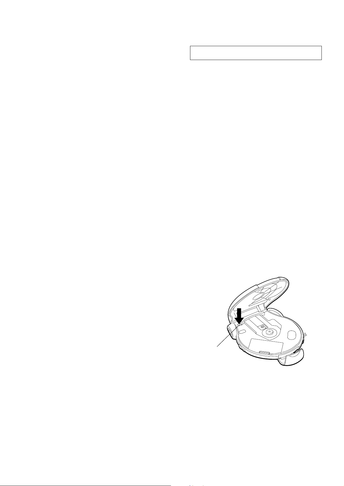
Method :
Emission of the laser diode is visually checked.
1. Open the upper lid.
2. Push the S801 as shown in Fig. 1 .
3. Check the object lens for confirming normal emission of the laser diode.
If not emitting, there is a trouble in the automatic power control circuit or
the optical pick-up. During normal operation, the laser diode is turned
ON about 2.5 seconds for focus searching.
7. ELECTRICAL PARTS LIST ·······································32
S801
Fig. 1 Method to push the S801
3
Page 4
D-FS601
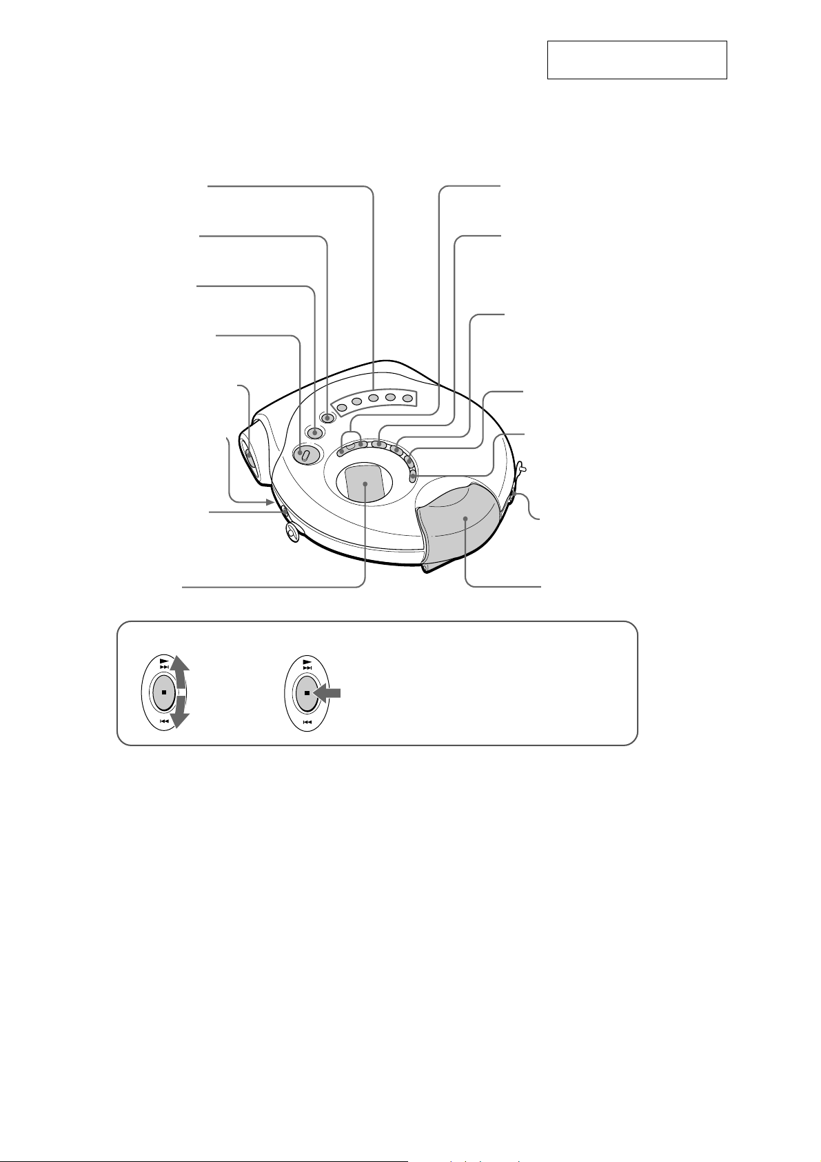
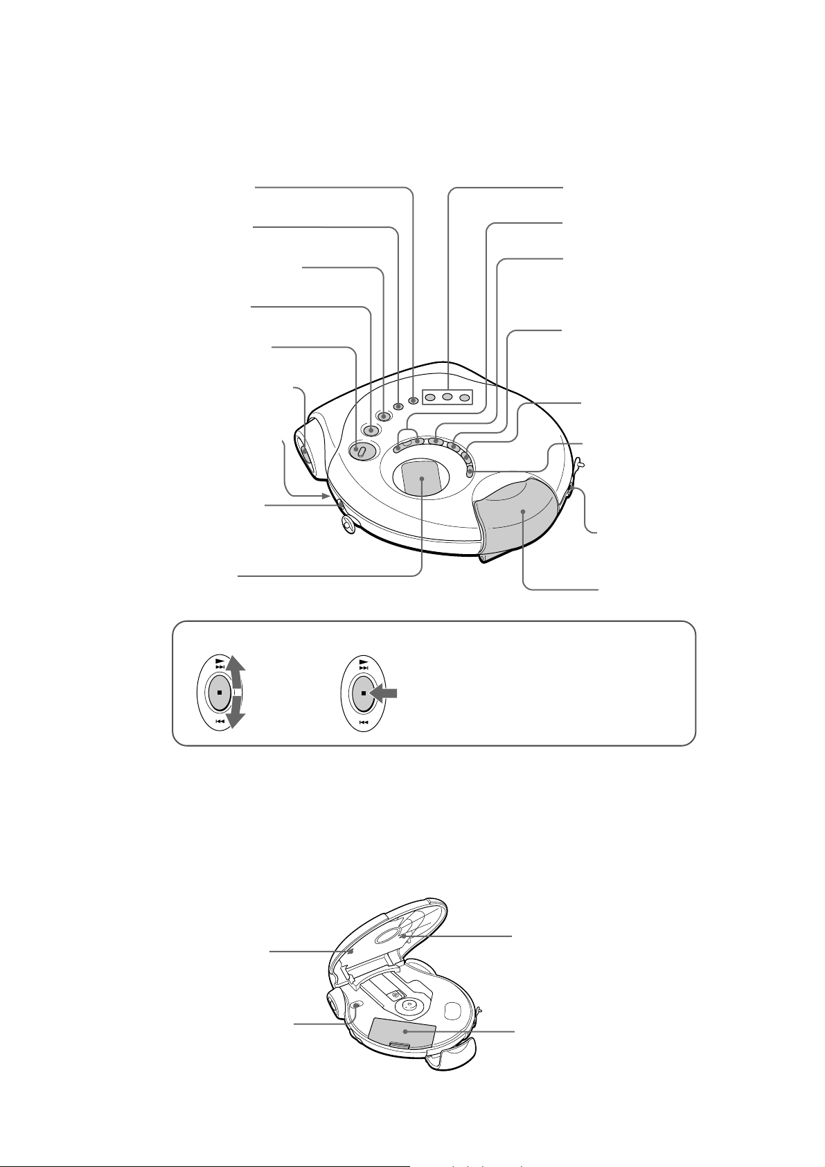
Locating The Controls
CD player (fornt)
(Except US model)
SECTION 2
GENERAL
This section is extracted from
instruction manual.
1 1 - 5 buttons
(page 14)
2 AM button
(pages 12, 15)
3 FM button
(pages 12, 15)
4 HOLD switch
(page 18)
5 3-way control key
(see below)
6 VOL* (volume)
control
(page 7)
7 DC IN 4.5 V
(external power
input) jack
(pages 6, 21)
9 PRESET –/+ buttons
(page 15)
q; REPEAT/ENTER•
TUNING + button
(pages 9 - 12, 15)
qa PLAY MODE•
TUNING – button
(pages 9 - 12, 15)
qs SOUND button
(pages 17, 18)
qd MEMORY button
(pages 14, 15)
qf i (headphones)
jack
(pages 6, 13, 20)
8 Display
(pages 8, 10 - 14, 17, 18)
5 3-way control key
Push toward
N/> or
..
* There is a tactile dot beside VOL to show the direction to turn up the volume.
** There is a tactile dot beside N/>.
Press x•
RADIO OFF/
CHG.
N/>**: Play/AMS/search
(pages 7, 8, 11)
.: AMS/search (pages 7, 11)
x•RADIO OFF/CHG:
Stop•charge/turn off the radio
(pages 7, 15, 19)
qg Buckle
(page 6)
4
Page 5
CD player (fornt)
(US model)
D-FS601
1 AM button
(pages 12, 15)
2 FM button
(pages 12, 15)
3 WB (weather band)
button (pages 12, 15)
4 TV button
(pages 12, 15)
5 HOLD switch
(page 18)
6 3-way control key
(see below)
7 VOL* (volume)
control
(page 7)
8 DC IN 4.5 V
(external power
input) jack
(pages 6, 21)
9 Display
(pages 8, 10 - 14, 17, 18)
q; 1 - 3 buttons
(page 14)
qa PRESET –/+ buttons
(page 15)
qs REPEAT/ENTER•
TUNING + button
(pages 9 - 12, 15)
qd PLAY MODE•
TUNING – button
(pages 9 - 12, 15)
qf SOUND button
(pages 17, 18)
qg MEMORY button
(pages 14, 15)
qh i (headphones)
jack
(pages 6, 13, 20)
qj Buckle
(page 6)
6 3-way control key
* There is a tactile dot beside VOL to show the direction to turn up the volume.
** There is a tactile dot beside N/>.
CD player (inside)
qk STEP switch
(page 16)
ql G-PROTECTION
switch
(page 17)
Push toward
N/> or
..
Press x•
RADIO OFF/
CHG.
N/>**: Play/AMS/search
(pages 7, 8, 11)
.: AMS/search (pages 7, 11)
x•RADIO OFF/CHG:
Stop•charge/turn off the radio
(pages 7, 15, 19)
w; LOCAL/DX switch
(page 13)
wa Battery compartment
(page 21)
5
Page 6
D-FS601
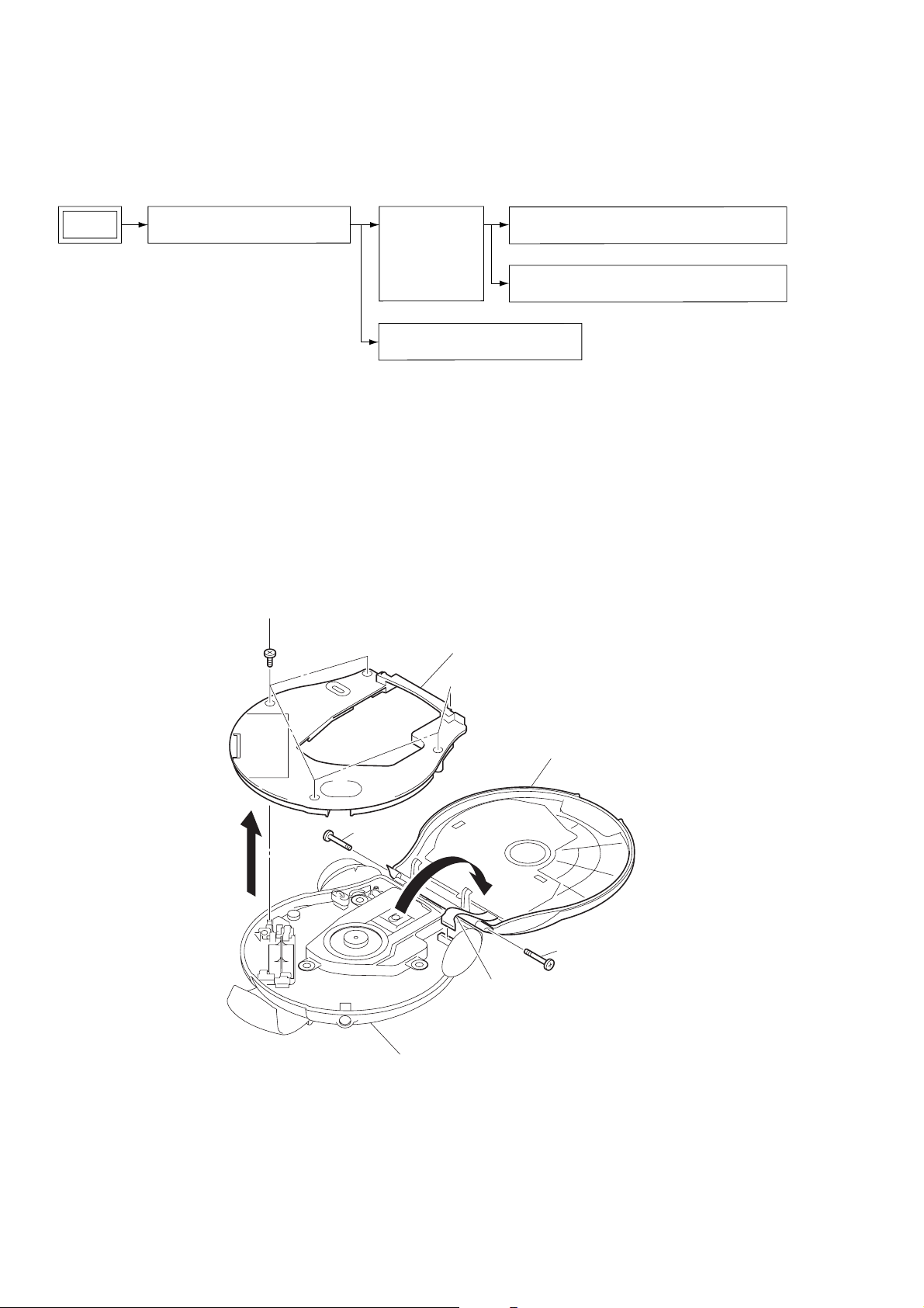
DISASSEMBLY
z
The equipment can be removed using the following procedure.
SECTION 3
SET
UPPER LID, MIDDLE CABINET
MD ASSY
(CDM-3125ER),
MAIN BOARD
SWITCH BOARD, HOLD LEVER
Note : Follow the disassembly procedure in the numerical order given.
3-1. Upper Lid, Middle Cabinet
3
five screws (B2)
middle cabinet
5
MOTOR ASSY, TURN TABLE (SPINDLE)(M901)
MOTOR ASSY, (SLED)(M902),
OPTICAL PICK-UP (DAX-25E)
4
1
screw
2
cabinet lower sub assy
7
6
flexible board
upper lid
1
screw
6
Page 7
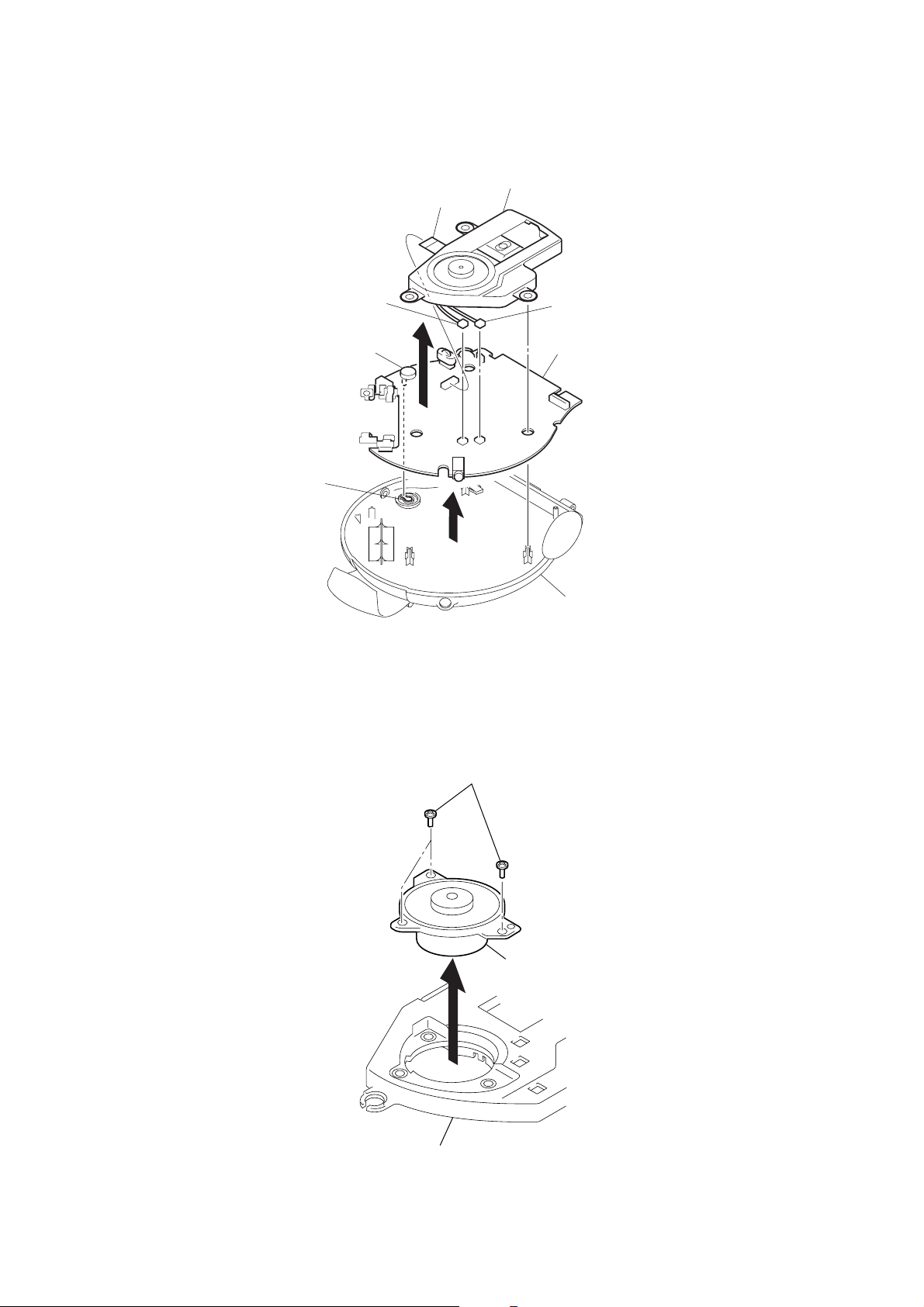
3-2. MD Assy (CDM-3125ER), MAIN Board
y
1
flexible cable (15P)
3
connector (CN502)(black)
RV301
lever(vol)(B)
4
5
MD ASSY (CDM-3125ER)
2
connector (CN503)(white)
7
MAIN board
D-FS601
3-3. Turn Table Motor Assy (Spindle) (M901)
6
1
three screws
(B1.7x5)
turn table motor ass
(spindle) (M901)
cabinet lower sub assy
2
chassis
7
Page 8
D-FS601
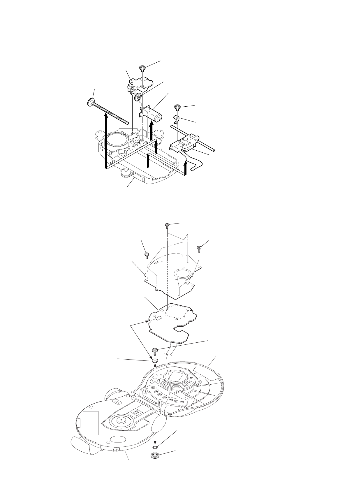
3-4. Motor Assy (Sled) (M902), Optical Pick-up (DAX-25E)
1
screw (B 1.7x5)
3
gear cover
gear B
9
screw assy, feed
5
8
2
4
motor assy (sled) (M902)
6
screw
(P 1.4x3.5)
7
bracket (Shaft)
qa
optical pick-up
(DAX-25E)
0
3-5. SWITCH Board, Hold Lever
When installing, align S903 with the
cut-out of the HOLD LEVER.
7
hold lever
chassis
2
four screws (B1.7 × 3)
4
cover lid
5
switch board
3
three screws (M1.4 × 2)
1
four screws (B1.7 × 3)
6
screw (B)
(1.4 × 4)
upper lid
9
O ring
When replacing the hold knob, coat here
with the specified grease (SGL-601).
8
hold knob
cabinet lower sub assy
8
Page 9
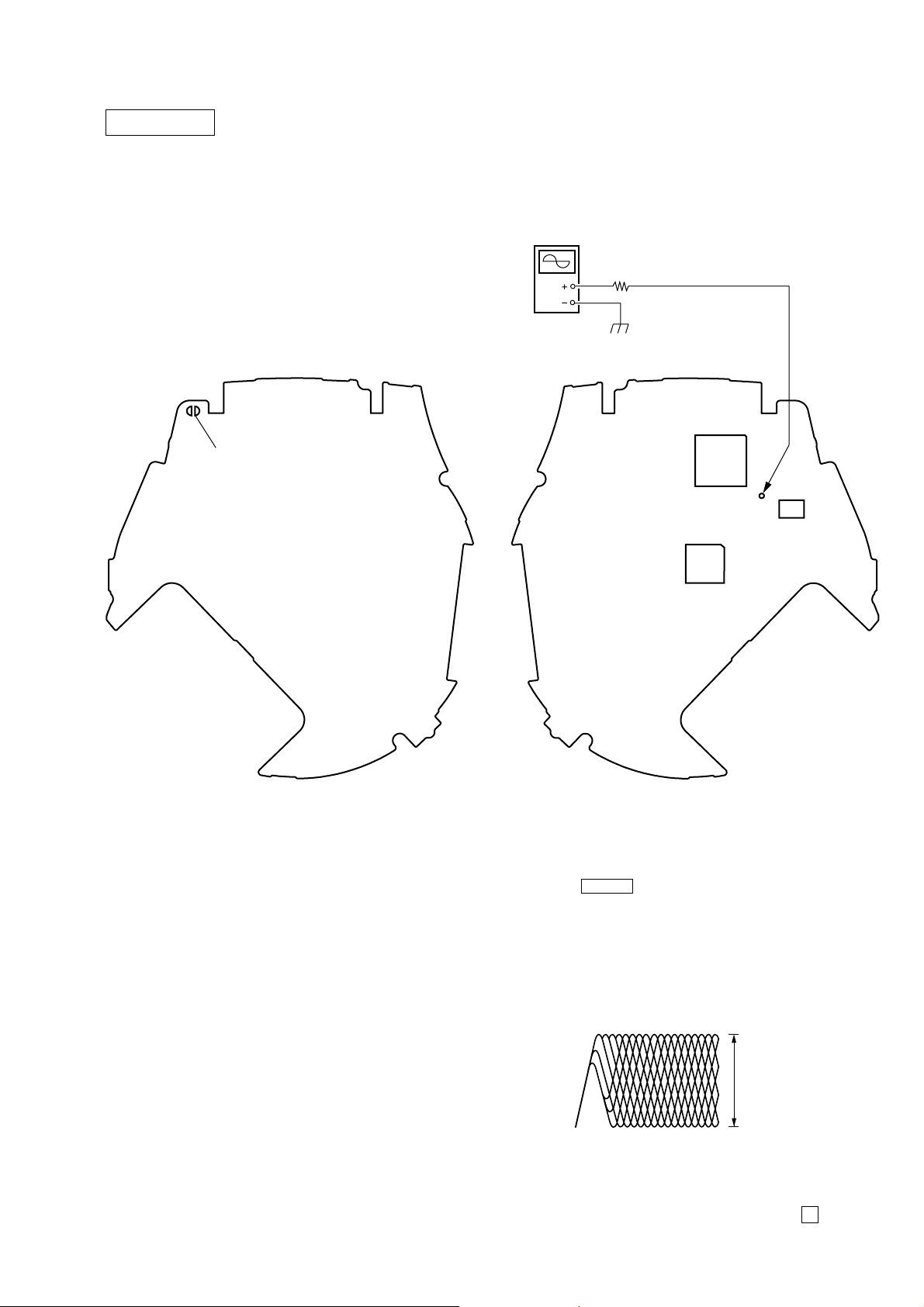
SECTION 4
)
TJ629 (RF)
2 K
Ω
Oscilloscope
(AC range)
IC601
IC801
IC302
ELECTRICAL ADJUSTMENTS
D-FS601
CD SECTION
The CD section adjustments are done automatically in this set.
Precautions for Check
1. Perform check in the order given.
2. Use YEDS-18 disc (Part No.: 3-702-101-01) unless otherwise
indicated.
3. Power supply voltage requirement : DC4.5 V in DC IN jack.
(J401)
VOLUME : Minimum
AVLS : OFF
HOLD switch : OFF
[MAIN BOARD] (Side A) [MAIN BOARD] (Side B)
TAP802 (OPEN)
Focus bias Check
Condition:
• Hold the set in horizontal state.
• Terminate TAP802 (open) by solder.
Connection:
Procedure:
1. Connect the oscilloscope to the test points TJ629 (RF) on the
MAIN board.
2. Set a disc. (YEDS-18)
3. Press the B/> button.
4. Check the oscilloscope waveform is as shown below.
A good eye pattern means that the diamond shape (◊) in the
center of the waveform can be clearly distinguished.
RF Signal reference Waveform (Eye Pattern)
VOLT/DIV : 100 mV (With the 10 : 1 probe in use
TIME/DIV : 500ns
RF level
0.4 to 0.5 Vp-p
To watch the eye pattern, set the oscilloscope to AC range and
increase the vertical sensitivity of the oscilloscope for easy
watching.
5. Stop revolving of the disc motor by pressing the x button.
9
Page 10
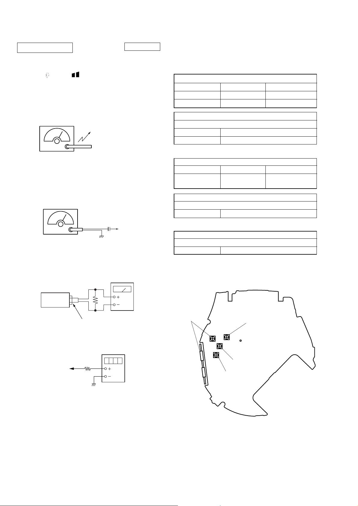
D-FS601
N
TUNER SECTION
• Switch Location
VOLUME : MAX
CT3, L3
AM TRACKING
L4
adjustment
AM FREQUENCY
COVERAGE asjustment
CT3
TJ8 (VT)
L5
L3
TV TRACKING
adjustment
L1
FM TRACKING
adjustment
BASS
AVLS : OFF
[AM]
BAND: AM
Signal generator
[FM]
BAND : FM
Signal generator
or BASS : OFF
AM RF signal
generator
30% amplitude modulation by 400Hz
signal.
Output level : as low as possible
FM RF signal
generator
75kHz(100%) amplitude modulation
by 1kHz signal.
Output level: as low as possible
Put the lead-wire
antenna close to
the set.
0.01µF
FM I
point
0 dB = 1 µV
•Repeat the procedures in each adjustment several times for the
maximum level meter indication.
•The AM tracking adjustments should be finally done by the
trimmer capacitors.
AM FREQUENCY COVERAGE ADJUSTMENT AND CHECK
Adjustment Part Frequency Display
Reading on Digital Voltmeter
L4 530kHz 1.2 ± 0.05V
Confirmation 1710kHz 7.6 ± 0.5V
AM TRACKING ADJUSTMENT
Adjust for a maximum reading on levelmeter
L3 620kHz
CT3 1400kHz
( ): US model
FM FREQUENCY COVERAGE CHECK
Adjustment Part Frequency Display
Confirmation
87.5MHz 4.2 ± 0.5V
(87.5MHz) (5.5 ± 0.5V)
Reading on Digital Voltmeter
FM TRACKING ADJUSTMENT
Adjust for a maximum reading levelmeter
L1 98.0MHz
US model only
TV TRACKING ADJUSTMENT
Adjust for a maximum reading on levelmeter
L5 ch10 197.75MHz
• Connecting levelmeter
set
J302 (
• Connecting digital voltmeter
TJ8 (VT)
i)
100k
16 Ω
Ω
levelmeter
digital voltmeter
Adjustment Location: Main board (Side B)
CT3, L3
AM TRACKING
adjustment
CT3
L3
L1
FM TRACKING
adjustment
L4
AM FREQUENCY
COVERAGE asjustment
TJ8 (VT)
L5
TV TRACKING
adjustment
10
Page 11
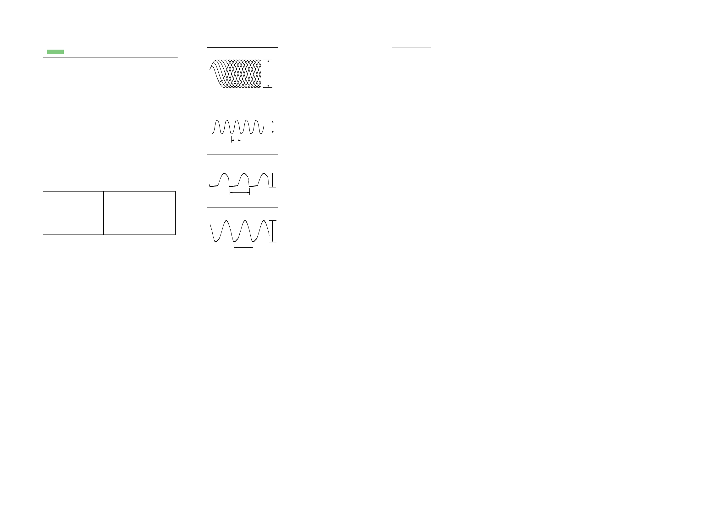
SECTION 5
DIAGRAMS
D-FS601
Note on Printed Wiring Board:
• X : parts extracted from the component side.
• : Pattern from the side which enables seeing.
Caution:
Pattern face side: Parts on the pattern face side seen from
(Side B) the pattern face are indicated.
Par ts face side: Parts on the parts face side seen from
(Side A) the parts face are indicated.
Note on Schematic Diagrams:
• All capacitors are in µF unless otherwise noted. pF: µµF
50 WV or less are not indicated except for electrolytics
and tantalums.
• All resistors are in Ω and 1/
specified.
¢
•
• 2 : nonflammable resistor.
• C : panel designation.
• H : adjustment for repair.
• A : B+ Line.
•Power voltage is dc 4.5 V and fed with regulated dc power
•Voltages and waveforms are dc with respect to ground
Note:
The components identified by mark 0 or dotted
line with mark 0 are criti-
cal for safety.
Replace only with part
number specified.
•Voltages are taken with a VOM (Input impedance 10 MΩ).
• Signal path.
: internal component.
supply from external power voltage jack.
under no-signal (detuned) conditions.
Voltage variations may be noted due to normal production tolerances.
F : FM
f : AM
J : CD
4
W or less unless otherwise
Note:
Les composants identifiés par
une marque 0 sont critiques
pour la sécurité.
Ne les remplacer que par une
piéce portant le numéro
spécifié.
• Waveforms
1
TEST POINT (TJ629,RF)
100mV/DIV, 400ns/DIV
2
IC601 rk (XTAO)
59ns
1V/DIV, 40ns/DIV
3
IC61 uf (XOUT)
13.3 µs
500mV/DIV, 4 µs/DIV
4
Q86 (collector)
327ns
1V/DIV, 100ns/DIV
MEMO
550mVp-p
2.5Vp-p
1.2Vp-p
3.7Vp-p
1111
Page 12
D-FS601
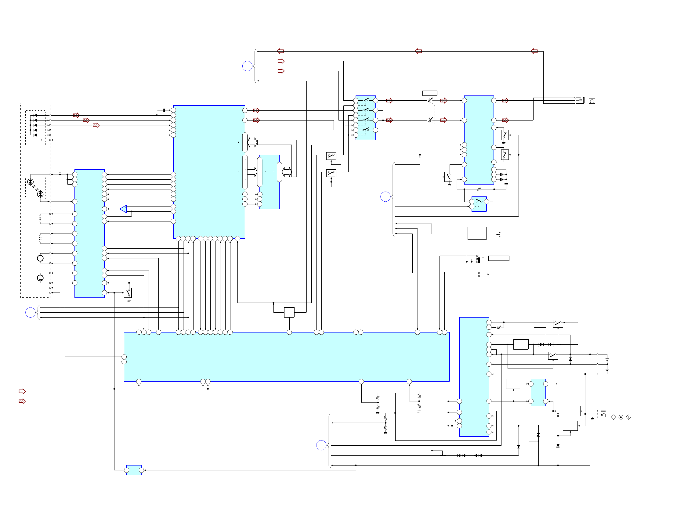
5-1. Block Diagrams – MAIN Section –
OPTICAL PICK-UP
DAX-25E
DETECTOR
LASER
DIODE
PD
FOCUS
COIL
TRACKING
COIL
M902
SLED
MOTOR
M901
SPINDLE
MOTOR
VCC
LD
OPGSW
M
M
OPSTB
RF
A
B
E
F
VCC1 2V
INM4
IC401(1/2)
COIL/MOTOR
LD
PD
F+
F-
T+
T-
S+
S-
C+
C-
69
38
36
26
24
34
32
30
28
2
5
3
VLOGO4
RF41
RF4
PAPC
FO1
RO1
FO4
RO4
FO2
RO2
FO3
RO3
DRIVE
MDP
DATA
CLOCK
APC REF
CHGMNT
WAKEUP
RESET
R11
R14
17F12
18R12
40F11
41
F14
21
22
19
11SYNC
20MDS
14
13
15POWERLATCH
7
58
12
16
IC402
4
Q410
FM ANT
TUNER
SECTION
IC601
RF AMP,SERVO,DSP,
D/A CONV,D-RAM CONT
84
RFAC
88
RFDC
92
A
91
B
89
E
90
F
100
SFDR
99
SRDR
96
FFDR
95
FRDR
98
TFDR
97
3
1
TRDR
103
MDP
104
C176
102
MDS
CLOCK
23
XLAT
FOK
SCOR
R4M
27
65
32
26
SENS
SDTO
21
20
22
WDCK
28
XRST
AOUT1
AOUT2
D0
D3
A0
A10
XWE
XCAS
XRAS
XSOE
MUTE
SYSM
24
25
61
TU-L
A
TU-R
TU MUTE
RV301
IC303
11 10
12
51
56
4
.
3
.
6
.
5
116
113
.
17
15
.
13
11
.
117
2
6
1
IC602
DRAM
9
12
.
15
19
.
21
.
8
4
23
5
A0
A10
XWE
XCAS
XRAS
2
.
D0
3
.
D3
24
.
25
Q307
Q308
VCPU
8
6
1
13
3
5
TUNER
SECTION
9
2
4
TU BEEP
XTU BASS1
C
TU BASS2
XTU AVLS
KEY
HOLD
OPEN
VOLUME
Q304
14
15
19
20
17
23
1
VCPU
HP AMP
LIN
RIN
MUTE
PWR SW
BEEP
BB SW
BST NF
2
4
S804
IC302
IC304
JOG
LOUT
ROUT
ALCIN
MIX OUT
1
2
1
8
6
12ALCDET
11
10
21BIAS
2ADDOUT
24BSTOUT
N
>
x
.
S802
G-PROTECTION
S801
(OPEN/CLOSE)
J302
Q305
Q306
TUNER
SECTION
B
• Signal Path
: FM
: CD
MSDTI
MSDTO
MSCK
77
HG_XSTB_O
78
HG_GUP_O
1
IC404
RESET
66
21
XWAKE_O
RESET
8
3
70
AGCPWM
AD CHGMNT
75
XPOWLT_O
16
17
MSDTI_I
MSDTO_O
18
15
XLAT_O
MSCK_O
11
36
SCOR_I
VDD1
5
VDD
2
FOK_I
VDD2
32
12
XIN_I
79
14
XRST_O
GRSCOR_I
13
XSOE_O
AMUTE_O
IC801(2/2)
SYSTEM CONTROL
Q601
MUTE
35
RESERVE
TUNER
SECTION
74
76
XTUAUDIO_O
XCDAUDIO_O
D
AD HI DC
VCPU
TU VCC
VIN
69
30
PWRSW_O
27
BEEP_O
AD_DCINMNT
4.5V
40
AD_BATMNT
22
IC303 VCC
HOLD_I
VIN
38
INM4
VCC1_2.0V
VCC2_3.3V
28
ESP_I
OPEN_LID_I
IC401(2/2)
POWER CONTROL
6
INM4
51
VCC1
74
VCC2
73
VLG3
RF3
INM3
VIN
STNG
VLGO2
VCPU
BATM1
BATM2
CHG SW
DC IN
D311D312
78
77
65
57
61
50
60
59
CHARGE
42
48
VG
9
LS
8
Q403
ON/OFF
Q408
SWITCH
D408
VDD
1
CHARGE
SWITCH
4
IC403
Q409
D801
Q405
2
3
D406
D401
D409
Q412
+B SWITCH
Q404
SWITCH
VCC1_2.0V
VCC2_3.3V
DRY BATTRY
SIZE "AA"
(IEC DESIGNATION LR6)
2PCS 3V
J401
DC IN 4.5V
1212
Page 13

– TUNER Section –
Q3
FM
LOCAL/DX
• Signal Path
AM FERRITE-BAR
: FM
S901
LOCAL/DX
S902
STEP
S927
PRESET +
S928
PRESET –
S903
HOLD
L3
ANTENNA
D3
LOCAL
DX
10kHz
9kHz
VCPU
ON
OFF
VCPU
VCPU
VCPU
EXCEPT US
US
Q84, 85
LPF
US
D1
D2
D5
AM OSC
T81,Q86
DC/DC
CONVERTER
FL2
B.P.F
FL1
B.P.F
L4
L1
FM RF
L12
TV/FM OSC
L5
TV RF
Q11
FMRFIN
2
TVRFIN
1
AMB/P
28
FMRFOUT
29
AMRFIN
27
FM/TVOSC
24
TVRFOUT
30
AMOSC
25
DETOUT
12
TU +B
S921-925
FUNCTION
KEY
S904, 905, 908-911
FUNCTION
KEY
FM-MIX
AM-MIX
MODE-1
MODE-2
OSCOUT
IFCOUNT
REQSW
Q10
+B SWITCH
FAV KEY
CD/TU KEY
QUAD
4
5
11
21
22
23
19
20
VCPU
Q4,5
+B SWITCH
IC1
FM /AM
IF/RF AMP
CF2,3
10.7MHz
450kHz
CF1
10.7MHz
Q2
CF1
V IN
8
10
FM-IFIN
AM IFIN
BAND
CONTROL
BAND
CONTROL
GL901
LIQUD
CRYSTAL
DISPLAY
Q6
Q7
L-OUT
R-OUT
Q60
Q62
16
15
IC62
EEPROM
DI
DO
SK
CS
3
4
2
1
X61
75kHz
IC61
DTS µCOM
59
BAND CTRL1-O
52
BAND CTRL2-O
71
AM IN
64
IF IN
60
+B ON/OFF_O
61
IFREQ-O
55
MONO OR LOCAL-O-CTR
30
EEP DO/DI-IO
31
EEP SK-O
32
EEP CS-O
65
EO(D01)_O
75
XIN
74
XOUT
1
COM0
4
COM3
5
20
25
LOCAL/MONO-DET-I
21
AM STEP-I
36
FAV KEY_I
27
PRESET+_I
26
PRESET-_I
XTUBASS1-O
TUAVLS CTRL_O
XLID OPEN-I
S1
S16
IC71
LINE AMP
21
67
TUMUTE-O
DEST0-I
DEST1-I
DEST2-I
SDO-O-CDU
SDI-I-CDU
SCK-I-CDU
ACK CD-O
LCDREQ-I
CD ON_I
RESET_I
TU ON_O
TUBEEP_O
TUBASS2-O
TU HOLD_I
VDD
AD DC REF
62
24
23
22
47
46
48
54
28
39
73
38
42KEY_I
37SC SEL_I
49
58
56
40
51
29
44 HIDC-I
72
45
VERSION SETTING
Q808
VCPU
IC801(1/2)
SYSTEM CONTROL
7
ACK_CD_I
9
ACK_CD_WAKE_I
39
LCDREQ_O
72
CDON_O
71
CD_RESET_TU-O
34
TUON_I
25
AD_KEY
73
SC_SEL_O
23
AD_FAV_KEY
33
KEY_INTERRUPT_I
TU_POWERON_O
IC81
+1.6V
2
REG
V IN
Q809
D-FS601
FM ANT
TU-L
MAIN
A
SECTION
TU-R
TU MUTE
MSDTO
MSDTI
MSCK
29
TU BEEP
XTU BASS1
TU BASS2
XTU AVLS
KEY
HOLD
OPEN
AD HI DC
VCPU
3
Q8,9
+B SWITCH
VIN
TU VCC
MAIN
B
SECTION
MAIN
C
SECTION
MAIN
D
SECTION
1313
Page 14

D-FS601
5-2. Printed Wiring Board – MAIN Board (Side A) –
: Uses unleaded solder.
IC402
IC62
IC81
• Semiconductor
Location
Ref. No. Location
D3 C-5
D311 D-3
D312 D-3
D321 B-2
D406 D-3
D407 D-3
D408 D-3
D409 E-4
D461 A-3
D805 C-3
IC403
IC62 A-4
IC81 B-4
IC402 B-3
IC403 C-2
Q3 D-5
Q10 C-3
Q84 B-3
Q305 B-1
Q307 A-3
Q308 A-3
Q403 C-2
Q404 D-4
Q408 D-4
Q409 D-4
Q410 D-3
Q412 C-1
1414
Page 15

D-FS601
5-3. Printed Wiring Board – MAIN Board (Side B) –
IC61
: Uses unleaded solder.
IC303
IC71
TJ8
(VT)
IC1
IC602
IC801
IC601
IC304
TJ629(RF)
IC302
• Semiconductor
Location
Ref. No. Location
D1 C-1
D2 C-1
D5 C-1
D80 C-3
D82 C-3
D401 C-4
D404 C-4
D601 A-3
D602 B-3
IC1 C-2
IC61 A-1
IC71 B-2
IC302 B-4
IC303 A-2
IC304 C-4
IC401 D-2
IC404 D-2
IC601 A-3
IC602 A-3
IC801 C-3
IC401
IC404
RECHARGEABLE
BATTERY
NH-WM2AA
2.4V
Q2 C-2
Q4 B-2
Q5 B-2
Q6 C-2
Q7 C-2
Q8 B-2
Q9 B-2
Q11 C-2
Q62 B-2
Q85 B-2
Q86 D-3
Q304 B-3
Q306 B-4
Q405 D-1
Q601 B-3
Q808 B-2
Q809 C-2
1515
Page 16

D-FS601
5-4. Schematic Diagram – MAIN Board (1/5) –
• See page 27 for IC Block Diagrams. • See page 11 for Waveforms.
IC B/D
(Page 18)
(Page 17)
1616
Page 17

D-FS601
5-5. Schematic Diagram – MAIN Board (2/5) –
• See page 25 for IC Pin Function Descriptions. • See page 11 for Waveforms.
(Page 16)
6
(Page 19)
NJRMP2
A
TO
SWITCH
BOARD
(Page 22)
1717
Page 18

D-FS601
5-6. Schematic Diagram – MAIN Board (3/5) –
(Page 16)
• See page 27 for IC Block Diagrams. • See page 11 for Waveforms.
(DAX-25E)
IC B/D
(RF)
(Page 19)
(Page 20)
1818
Page 19

5-7. Schematic Diagram – MAIN Board (4/5) –
D-FS601
(Page 18)
(Page 20)
6
(Page 17)
1919
Page 20

D-FS601
5-8. Schematic Diagram – MAIN Board (5/5) –
• See page 23 for IC Pin Function Descriptions.
(Page 18)
(JOG)
N
>
x
.
(Page 19)
X_TU_MUTE_O
2020
Page 21

5-9. Printed Wiring Board – SWITCH Board – : Uses unleaded solder.
D-FS601
2121
Page 22

D-FS601
5-10. Schematic Diagram – SWITCH Board –
(2/5)
(Page 17)
2222
Page 23

5-11. IC Pin Function Descriptions
• IC801 T5AW5-SPTU-MP1 System Controller (MAIN Board)
D-FS601
Pin No.
1
2
3
4
5
6
7
8
9
10
11
12
13
14
15
16
17
18
19
20
21
22
23
24
25
26
27
28
29
30
31
32
33
34
35
36
37
38
39
40
41 to 56
57 to 60
61 to 63
64, 65
66
67
68
69
70
Pin Name
GND
XIN
XOUT
TEST
VDD1
PRESET–
ACK_CD_I
RESET
ACK_CD_WAKE_I
RESERVE
SCOR_I
GRSCOR_I
AMUTE_O
XSOE_O
XLAT_O
MSDTI_I
MSDTO_O
MSCK_O
VCPU_AD
VREF_AD
AD_CHGMNT
AD_BATMNT
AF_FAV_KEY
AD_CDTEST
AD_KEY
AD_RMKEY
AD_DCINMNT
OPEN_LID_I
TU_POWERON_O
BEEP_O
TSB_I/O
VDD2
KEY_INTERRUPT_I
TUON_I
X_TU_MUTE_O
FOK_I
XL/O_I
ESP_I
LCDREQ_O
HOLD_I
SEG15 to SEG0
COM3 to COM0
V3 to V1
C1, C0
XWAKE_O
PGMSO_O
PGMSI_I
PGMSCK_O/
PWSWR_O
AGCPWM_O
I/O
—
Ground (digital)
I
Clock input
O
Clock output Not used (open)
I
Shipment test pin (connected to ground)
—
Power supply (2.0V)
I
PRESET– signal input (not ured)
I
Acknowledgement and status signal input from the DTS (IC61)
I
Reset signal input from the reset IC (IC404)
I
Wa ke up signal input from the DTS (IC61)
I
Selector for NJR TU or NJR SP TU (fixed at “H”)
I
Sub-code sync detection signal input from the DSP (IC601)
I
GRSCOR signal input from the DSP (IC601)
O
Muting control signal output to the DSP (IC601)
O
Serial data output enable signal output to the DSP (IC601)
O
Serial data latch signal output to DSP (IC601)
I
Serial data input from the DSP (IC601) and the DTS (IC61)
O
Serial data output to the DSP (IC601) and the DTS (IC61)
O
Serial clock output to the DSP (IC601) and the DTS (IC61)
I
Reference voltage input terminal (high)
I
Reference voltage input terminal
I
Battery charge voltage monitoring signal input from the IC401
I
Battery voltage monitoring signal input
I
Favorite key signal input
I
CD test mode on signal input
I
Key signal input
I
Key signal input from the remote commander (fixed at “L”)
I
DC input voltage monitoring signal input
I
CD lid open/close detection signal input from the S801
O
Power control signal output to the DTS block
O
Beep sound signal output to the headphone amplifier (IC302)
I/O
Not used (open)
—
Power supply
I
Key input detection interrupt signal input during sleep mode
I
Radio mode status signal input
O
DTS muting disable signal output during CD playback
I
Focus OK signal input from the DSP (IC601)
I
Line out jack detection signal input (fixed at “H”)
I
G-PROTECTION switch signal input from the S802
O
Communication sync signal output to the DTS (IC61)
I
HOLD switch signal input from the S903
O
Not used (open)
O
Not used (open)
—
Not used (open)
—
Not used (open)
O
Wa ke up signal output to the IC401
O
Not used (open)
I
Not used (open)
O
Headphone amplifier power control signal output
O
AGC PWM signal output to the IC401
Description
23
Page 24

D-FS601
Pin No.
71
72
73
74
75
76
77
78
79
80
Pin Name
CD_RESET_TU_O
CDON_O
PGMSEL_O/
SC_SEL_O
XTUAUDIO_O
XPOWLT_O
XCDAUDIO_O
HG_XSTB_O
HG_GUP_O
XRST_O
PRESET+
I/O
O
Reset signal output to the DTS (IC61)
O
CD mode status signal output to the DTS (IC61)
O
Serial communication selector between the DTS and the DSP signal output to the DTS (IC61)
O
Tuner audio on signal output
O
Power latch signal output to the IC401
O
CD audio on signal output
O
Optical pickup standby control signal output to the optical pickup block
O
Optical pickup gain up (for CD-RW) control signal output to the optical pickup block
O
Reset signal output to the DSP (IC601)
I
PRESET+ signal input (not ured)
Description
24
Page 25

• IC61 TC9327AF-NJRMP2 RF AMP, SERVO, DSP, D/A CONV, D-RAM CONT (MAIN Board)
D-FS601
Pin No.
1 to 4
5 to 20
21
22
23
24
25
26
27
28
29
30
31
32
33
34
35
36
37
38
39
40
41
42
43
44
45
46
47
48
49
50
51
52
53
54
55
56
57
58
59
60
61
62
63
64
65
66
Pin Name
COM1 to COM4
S1 to S16
AM STEP-I
DEST2-I
DEST1-I
DEST0-I
LOCAL/
MONO-DET-I
PRESET–_I
PRESET+_I
LCDREQ-I
XLID OPEN-I
EEP DO/DI-IO
EEP SK-O
EEP CS-O
XL/O-I
RMKEY_I
NC
FAV KEY_I
SC SEL_I
TU ON_O
CD ON_I
TUAVLS CTRL_O
TV-L ON_O
KEY_I
BATT_I
HIDC_I
AD DC REF
SDI-I-CDU
SDO-O-CDU
SCK-I-CDU
TUBEEP_O
PLAY KEY CTRL_O
TU HOLD_I
BAND CTRL 2_O
DC IN DET-I
ACK CD-O
MONO OR
LOCAL-O-CTR
TUBASS2-O
XTU TEST_I
XTUBASS1-O
BAND CTRL 1_O
+B ON/OFF-O
IFREQ-O
TUMUTE-O
TEST
IFIN_I
EO(DO1)_O
NC(DO2)
I/O
O
LCD drivers
O
LCD drivers
I
AM 9K/10K tuning step select (initialisation) signal input
I
Bit 2 Tu Destination setting input
I
Bit 1 Tu Destination setting input
I
Bit 0 Tu Destination setting input
I
Local/DX or Mono/Stereo ON-Off switch detection signal input
I
PRESET– signal input from the S928
I
PRESET+ signal input from the S927
I
LCD display request signal from the IC801
I
CD lid open/close detection signal input from the S801
I/O
Data input/output for EEPROM
O
Clock output for EEPROM 2K bits (software timing)
O
Chip select signal output for EEPROM
I
Line out jack detection signal input (fixed at “H”)
I
Key signal input from the remote commander
O
Not used
I
Favorite key signal input
I
Serial communication selector signal input from the IC801
O
Radio mode status signal output to the IC801
I
CD ON request signal input from the IC801 (Wakeup TU in sleep mode)
O
AVLS control signal output
O
TV-L (ch 2, 3 and 4) selection switch control signal output (not ured)
I
Key signal input from the function keys
I
Battery voltage detection signal input (external DC 1.6V as reference)
I
HiDC voltage detection signal input
—
DC reference of A/D converter (used for HiDC and batt detection with external DC 1.6V as reference)
I
Serial data input from the IC801
O
Serial data output to the IC801
I
Serial clock input from the IC801
O
Beep sound signal output to the headphone amplifier
O
Play key detection control signal output for CD mode (not ured)
I
HOLD switch detection signal input from the S903
O
BAND CONTROL 2 signal output
I
DC-in detection signal input
O
CD acknowledgement and status signal output to the IC801
O
Local/DX or Mono/Stereo ON-Off control signal output
O
Mega Bass 2 (sound mode) control signal output
I
TU test mode detection signal input (“L” : active)
O
Mega Bass 1 (sound mode) control signal output
O
BAND CONTROL 1 signal output
O
Radio power On/Off control signal output (VCO and IF amplifier block)
O
IF request signal output
O
Tuner muting control signal output
—
Not used (open)
I
TV/WB/FM/AM IF signal input
O
PLL error signal output
—
Not used (open)
Description
25
Page 26

D-FS601
Pin No.
67
68
69
70
71
72
73
74
75
76
77
78
79
80
Pin Name
HOLD_I
NC (OT1)
GND
FM IN
AM IN
VDD(1.8-2.2V)
RESET_I
XOUT
XIN
VXT
VLCD
C1
C2
VEE
I/O
I
Not used (connected to ground)
O
Not used (open)
—
Ground
I
Not used (open)
I
TV/WB/FM/AM OSC signal input
—
VDD power supply
I
Reset signal input from the IC801
O
Crystal oscillator terminal
I
Crystal oscillator terminal
—
Crystal oscillator terminal
—
LCD voltage doubler
—
LCD voltage doubler
—
LCD voltage doubler
—
Constant voltage for LCD 1.55V
Description
26
Page 27

5-12. IC Block Diagrams
IC71 NJM2100E
D-FS601
A-OUT
A –
A +
V–
IC302 TA2120FN
BB
BST
SW
OUT
24
23
ADD
B
BST
+
–
ADD
1
+
–
2
+
3
4
BIAS
BIAS
IN
21
22
BIAS
A
V+
8
B-OUT
7
–
B –
6
B +
5
PWR
SW
20 19 18
PWSWMT
SW
+
–
PW
B
OUT B
PW
C
BEEP
17
BEEP
+
PW
A
ATT
LINRINGNDMUTE_τMUTE
15
16
ALC ALC
OUT A
–
SW
13
14
ATT
SW
1
BSTNFADD
OUT
PWC
SW
8
2
3
RF IN OCL
SW
4 5
VCC
7
6
ROUT VREF LOUT
9
PGND
10
MIX
OUT
ALC
DET
11
ALCINALC
DET
12
27
Page 28

D-FS601
NOTE:
• -XX, -X mean standardized parts, so they may
have some differences from the original one.
• Items marked “*” are not stocked since they
are seldom required for routine service. Some
delay should be anticipated when ordering these
items.
6-1. Upper Lid Section
SECTION 6
EXPLODED VIEWS
• The mechanical parts with no reference number
in the exploded views are not supplied.
• Accessories are given in the last of this parts
list.
The components identified by mark 0 or
dotted line with mark 0 are critical for safety.
Replace only with part number specified.
Les composants identifiés par une marque
0 sont critiques pour la sécurité.
Ne les remplacer que par une pièce portant
le numéro spécifié.
12
11
13
10
9
8
7
6
2
14
a
15
2
2
16
13
a
GL901
3
not
supplied
1
cabinet section
not
supplied
2
4
Ref. No. Part No. Description Remarks Ref. No. Part No. Description Remarks
1 X-3382-543-1 COVER (SVX) ASSY, LID
2 3-343-254-31 SCREW (B1.7X3), TAPPING
* 3 A-3178-670-A SWITCH BOARD, COMPLETE
4 3-338-687-21 SCREW (M1.4X2), TAPPING
5 3-238-012-01 RING, UPPER LID
6 3-245-012-01 RUBBER,CONNECTOR
7 3-243-360-01 HOLDER (LCD)
8 3-318-201-51 SCREW (B) (1.4X4), TAPPING
9 3-238-008-01 LEVER, HOLD
5
2
10 X-3382-540-1 LID (SVX) ASSY, UPPER (US)
10 X-3382-542-1 LID (SVX) ASSY, UPPER (CND)
11 3-221-329-01 RING, O
12 3-238-021-01 KNOB, HOLD
13 3-238-478-01 SCREW, TAPPING
14 3-238-004-01 GRIP
15 3-238-013-01 ARM, A
16 3-238-025-01 PACKING (UPPER LID)
GL901 1-804-638-11 LCD
28
Page 29

6-2. Cabinet Section
52
Optical Pick-Up section
(CDM-3125ER)
51
D-FS601
54
53
55
64
not
supplied
59
60
61
58
BT400
58
54
BT402
BT401
65
62
not
supplied
57
5666
67
63
68
cabinet lower section
Ref. No. Part No. Description Remarks Ref. No. Part No. Description Remarks
51 3-237-999-01 CABINET, MIDDLE
52 3-238-001-01 LID, BATTERY
53 3-238-014-01 ARM, B
54 4-908-792-51 SCREW (B2)
55 3-343-254-31 SCREW (B1.7X3), TAPPING
56 1-685-380-11 PWB, FLEXIBLE
57 4-223-609-01 KNOB (JOGGABLE)
58 4-225-316-01 ROLLER
59 X-3381-669-1 BUCKLE SUB ASSY
60 3-221-309-01 LEVER (VOL) (A)
61 4-223-413-01 SCREW (M1.4X3)
62 3-577-414-01 SPACER
* 63 A-3178-669-A MAIN BOARD, COMPLETE (US)
* 63 A-3178-676-A MAIN BOARD, COMPLETE (CND)
64 X-3381-670-1 BRACKET ROLLER ASSY
65 3-338-687-21 SCREW (M1.4X2), TAPPING
66 3-245-532-01 COPPER SHEET
67 3-245-576-01 SHEET, INSULATING (PWB)
68 3-245-910-01 COPPER SHEET (B)
BT400 3-238-476-01 TERMINAL, BATTERY (+)
BT401 3-238-477-01 TERMINAL, BATTERY LINK
BT402 3-221-307-01 TERMINAL BOARD (-), BATTERY
29
Page 30

D-FS601
6-3. Cabinet Lower Section
105
101
107
103
110
not
supplied
104
109
102
113
103
105
106
105
111
112
105
114
108
115
105
Ref. No. Part No. Description Remarks Ref. No. Part No. Description Remarks
101 3-238-023-01 BUTTON, JOG
102 3-238-017-01 RUBBER, SHIELD
103 3-318-201-51 SCREW (B) (1.4X4), TAPPING
104 3-238-016-01 JOG, ACTUATOR
105 4-908-792-31 SCREW (B2)
106 3-238-010-01 SHEET, ADHESIVE
107 3-238-019-01 PLATE (JOG)
108 3-238-002-01 STRAP, BRACKET
109 3-238-020-11 PLATE (JOG)
110 3-221-310-01 LEVER (VOL) (B)
111 X-3381-668-1 CABINET LOWER SUB ASSY
112 3-238-015-01 PLATE, ORNAMENTAL
113 3-221-311-11 PACKING (H/P)
114 3-221-329-01 RING, O
115 3-238-007-01 KNOB, VOLUME
30
Page 31

6-4. Optical Pick-up Section (CDM-3125ER)
156
D-FS601
164
152
M901
157
156
155
153
154
152
156
M902
151
158
159
163
160
161
162
Ref. No. Part No. Description Remarks Ref. No. Part No. Description Remarks
151 4-218-821-01 COVER, GEAR
152 3-318-203-71 SCREW (B1.7X5), TAPPING
153 A-3052-902-A FEED ASSY, SCREW
154 4-218-823-01 GEAR (B)
155 4-218-825-01 SPRING, SLED
156 4-222-765-01 INSULATOR
157 3-235-420-01 CHASSIS
158 4-218-827-01 RETAINER, SHAFT
159 3-686-458-03 SCREW (P1.4X3.5), TAPPING
0 160 X-3380-950-1 OPTICAL PICK-UP (DAX-25E)
161 3-235-418-01 RACK
162 3-348-998-81 SCREW (M1.4)
163 4-220-645-01 SHAFT, STANDARD
164 3-243-233-01 SPACER, CDM
M901 A-3052-904-A MOTOR ASSY, TURN TABLE (SPINDLE)
M902 A-3328-627-A MOTOR ASSY, SLED (SLED)
The components identified by
mark 0 or dotted line with mark
0 are critical for safety.
Replace only with part number
specified.
Les composants identifiés par
une marque 0 sont critiques
pour la sécurité.
Ne les remplacer que par une
pièce portant le numéro spécifié.
31
Page 32

D-FS601
MAIN
SECTION 7
ELECTRICAL PARTS LIST
NOTE:
• Due to standardization, replacements in the
parts list may be different from the parts
specified in the diagrams or the components
used on the set.
• -XX, -X mean standardized parts, so they may
have some difference from the original one.
• RESISTORS
All resistors are in ohms.
METAL: metal-film resistor
METAL OXIDE: Metal Oxide-film resistor
F: nonflammable
Ref. No. Part No. Description Remarks Ref. No. Part No. Description Remarks
* A-3178-669-A MAIN BOARD, COMPLETE (US)
* A-3178-676-A MAIN BOARD, COMPLETE (CND)
**************************
< BATTERY TERMINAL >
BT400 3-238-476-01 TERMINAL, BATTERY (+)
BT401 3-238-477-01 TERMINAL, BATTERY LINK
BT402 3-221-307-01 TERMINAL BOARD (-), BATTERY
< CAPACITOR >
C2 1-162-908-11 CERAMIC CHIP 3PF 0.25PF 50V
C4 1-162-997-11 CERAMIC CHIP 10PF 0.5PF 50V
C6 1-162-970-11 CERAMIC CHIP 0.01uF 10% 25V
C8 1-164-227-11 CERAMIC CHIP 0.022uF 10% 25V
C9 1-162-927-11 CERAMIC CHIP 100PF 5% 50V
C10 1-162-970-11 CERAMIC CHIP 0.01uF 10% 25V
C11 1-164-227-11 CERAMIC CHIP 0.022uF 10% 25V
C12 1-162-923-11 CERAMIC CHIP 47PF 5% 50V
C13 1-162-927-11 CERAMIC CHIP 100PF 5% 50V
C15 1-164-315-11 CERAMIC CHIP 470PF 5.00% 50V
C20 1-125-891-11 CERAMIC CHIP 0.47uF 10.00% 10V
C21 1-162-927-11 CERAMIC CHIP 100PF 5% 50V
C22 1-162-970-11 CERAMIC CHIP 0.01uF 10% 25V
C23 1-162-970-11 CERAMIC CHIP 0.01uF 10% 25V
C24 1-164-227-11 CERAMIC CHIP 0.022uF 10% 25V
C26 1-162-927-11 CERAMIC CHIP 100PF 5% 50V
C27 1-162-970-11 CERAMIC CHIP 0.01uF 10% 25V
C28 1-162-970-11 CERAMIC CHIP 0.01uF 10% 25V
C29 1-162-970-11 CERAMIC CHIP 0.01uF 10% 25V
C30 1-115-156-11 CERAMIC CHIP 1uF 10V
C31 1-115-156-11 CERAMIC CHIP 1uF 10V
C32 1-135-151-21 TANTALUM CHIP 4.7uF 20% 4V
C33 1-162-964-11 CERAMIC CHIP 0.001uF 10% 50V
C34 1-107-826-11 CERAMIC CHIP 0.1uF 10.00% 16V
C35 1-164-315-11 CERAMIC CHIP 470PF 5.00% 50V
C36 1-162-970-11 CERAMIC CHIP 0.01uF 10% 25V
C39 1-164-227-11 CERAMIC CHIP 0.022uF 10% 25V
C40 1-109-935-11 TANTAL. CHIP 4.7uF 20.00% 4V
C41 1-165-176-11 CERAMIC CHIP 0.047uF 10.00% 16V
C42 1-216-864-11 METAL CHIP 0 5% 1/16W
C43 1-117-863-11 CERAMIC CHIP 0.47uF 10.00% 6.3V
C44 1-216-864-11 METAL CHIP 0 5% 1/16W
• Items marked “*” are not stocked since they
are seldom required for routine service.
Some delay should be anticipated when
ordering these items.
• SEMICONDUCTORS
In each case, u: µ, for example:
uA...: µA... , uPA... , µPA... ,
uPB... , µPB... , uPC... , µPC... ,
uPD..., µPD...
• CAPACITORS:
uF: µF
• COILS
uH: µH
C45 1-113-690-11 ELECT CHIP 220uF 20.00% 4V
C46 1-115-416-11 CERAMIC CHIP 0.001uF 5.00% 25V
C50 1-164-156-11 CERAMIC CHIP 0.1uF 25V
C52 1-162-970-11 CERAMIC CHIP 0.01uF 10% 25V
C53 1-162-970-11 CERAMIC CHIP 0.01uF 10% 25V
C54 1-107-826-11 CERAMIC CHIP 0.1uF 10.00% 16V
C56 1-162-970-11 CERAMIC CHIP 0.01uF 10% 25V
C62 1-162-964-11 CERAMIC CHIP 0.001uF 10% 50V
C63 1-162-919-11 CERAMIC CHIP 22PF 5% 50V
C64 1-162-915-11 CERAMIC CHIP 10PF 0.5PF 50V
C65 1-107-823-11 CERAMIC CHIP 0.47uF 10.00% 16V
C66 1-107-826-11 CERAMIC CHIP 0.1uF 10.00% 6V
C67 1-107-826-11 CERAMIC CHIP 0.1uF 10.00% 16V
C68 1-107-823-11 CERAMIC CHIP 0.47uF 10.00% 16V
C69 1-104-852-11 TANTAL. CHIP 22uF 20.00% 6.3V
C70 1-162-970-11 CERAMIC CHIP 0.01uF 10% 25V
C71 1-164-230-11 CERAMIC CHIP 220PF 5.00% 50V
(US)
(US)
(US)
C72 1-164-230-11 CERAMIC CHIP 220PF 5.00% 50V
C73 1-164-230-11 CERAMIC CHIP 220PF 5.00% 50V
C74 1-164-230-11 CERAMIC CHIP 220PF 5.00% 50V
C75 1-162-927-11 CERAMIC CHIP 100PF 5% 50V
C76 1-162-927-11 CERAMIC CHIP 100PF 5% 50V
C79 1-104-852-11 TANTAL. CHIP 22uF 20.00% 6.3V
C80 1-162-970-11 CERAMIC CHIP 0.01uF 10% 25V
C81 1-162-964-11 CERAMIC CHIP 0.001uF 10% 50V
C82 1-164-489-11 CERAMIC CHIP 0.22uF 10.00% 16V
C83 1-162-927-11 CERAMIC CHIP 100PF 5% 50V
C84 1-162-970-11 CERAMIC CHIP 0.01uF 10% 25V
C85 1-164-505-11 CERAMIC CHIP 2.2uF 16V
C86 1-162-915-11 CERAMIC CHIP 10PF 0.5PF 50V
C87 1-162-915-11 CERAMIC CHIP 10PF 0.5PF 50V
C88 1-162-970-11 CERAMIC CHIP 0.01uF 10% 25V
C89 1-162-964-11 CERAMIC CHIP 0.001uF 10% 50V
C90 1-104-852-11 TANTAL. CHIP 22uF 20.00% 6.3V
C91 1-162-970-11 CERAMIC CHIP 0.01uF 10% 25V
C92 1-115-156-11 CERAMIC CHIP 1uF 10V
C96 1-115-156-11 CERAMIC CHIP 1uF 10V
C101 1-117-720-11 CERAMIC CHIP 4.7uF 10V
C104 1-162-927-11 CERAMIC CHIP 100PF 5% 50V
C105 1-115-156-11 CERAMIC CHIP 1uF 10V
C110 1-124-635-00 ELECT 220uF 20.00% 6.3V
C145 1-107-826-11 CERAMIC CHIP 0.1uF 10.00% 16V
C153 1-110-569-21 TANTAL. CHIP 47uF 20.00% 4V
•Abbreviation
CND : Canadian model
US : US model
The components identified by mark 0 or
dotted line with mark 0 are critical for safety.
Replace only with part number specified.
Les composants identifiés par une marque
0 sont critiques pour la sécurité.
Ne les remplacer que par une pièce portant
le numéro spécifié.
When indicating parts by reference number,
please include the board name.
32
Page 33

D-FS601
MAIN
Ref. No. Part No. Description Remarks Ref. No. Part No. Description Remarks
C154 1-162-970-11 CERAMIC CHIP 0.01uF 10% 25V
C157 1-164-227-11 CERAMIC CHIP 0.022uF 10% 25V
C158 1-162-910-11 CERAMIC CHIP 5PF 0.25PF 50V
C160 1-162-923-11 CERAMIC CHIP 47PF 5% 50V
C162 1-162-970-11 CERAMIC CHIP 0.01uF 10% 25V
C164 1-115-156-11 CERAMIC CHIP 1uF 10V
C166 1-162-970-11 CERAMIC CHIP 0.01uF 10% 25V
C167 1-162-970-11 CERAMIC CHIP 0.01uF 10% 25V
C168 1-162-964-11 CERAMIC CHIP 0.001uF 10% 50V
C169 1-165-176-11 CERAMIC CHIP 0.047uF 10.00% 16V
C201 1-117-720-11 CERAMIC CHIP 4.7uF 10V
C204 1-162-927-11 CERAMIC CHIP 100PF 5% 50V
C205 1-115-156-11 CERAMIC CHIP 1uF 10V
C210 1-124-635-00 ELECT 220uF 20.00% 6.3V
C245 1-107-826-11 CERAMIC CHIP 0.1uF 10.00% 16V
C302 1-216-864-11 METAL CHIP 0 5% 1/16W
C313 1-128-705-11 ELECT 100uF 6.3V
C317 1-162-964-11 CERAMIC CHIP 0.001uF 10% 50V
C318 1-164-156-11 CERAMIC CHIP 0.1uF 25V
C319 1-164-156-11 CERAMIC CHIP 0.1uF 25V
C333 1-115-156-11 CERAMIC CHIP 1uF 10V
C351 1-115-156-11 CERAMIC CHIP 1uF 10V
C352 1-124-261-00 ELECT 10uF 20% 50V
C353 1-135-210-11 TANTALUM CHIP 4.7uF 20% 10V
C354 1-126-369-11 ELECT 220uF 20% 6.3V
C355 1-115-156-11 CERAMIC CHIP 1uF 10V
C356 1-115-467-11 CERAMIC CHIP 0.22uF 10.00% 10V
C357 1-107-826-11 CERAMIC CHIP 0.1uF 10.00% 16V
C358 1-164-505-11 CERAMIC CHIP 2.2uF 16V
C359 1-107-826-11 CERAMIC CHIP 0.1uF 10.00% 16V
C401 1-162-970-11 CERAMIC CHIP 0.01uF 10% 25V
C403 1-162-968-11 CERAMIC CHIP 0.0047uF 10% 50V
C405 1-165-176-11 CERAMIC CHIP 0.047uF 10.00% 16V
C406 1-135-259-11 TANTAL. CHIP 10uF 20.00% 6.3V
C407 1-125-837-91 CERAMIC CHIP 1uF 10% 6.3V
C409 1-124-584-00 ELECT 100uF 20% 10V
C410 1-124-584-00 ELECT 100uF 20% 10V
C411 1-162-970-11 CERAMIC CHIP 0.01uF 10% 25V
C412 1-124-635-00 ELECT 220uF 20.00% 6.3V
C413 1-162-970-11 CERAMIC CHIP 0.01uF 10% 25V
C414 1-162-966-11 CERAMIC CHIP 0.0022uF 10% 50V
C415 1-164-156-11 CERAMIC CHIP 0.1uF 25V
C416 1-164-156-11 CERAMIC CHIP 0.1uF 25V
C417 1-110-569-21 TANTAL. CHIP 47uF 20.00% 4V
C418 1-126-369-11 ELECT 220uF 20% 6.3V
C419 1-135-259-11 TANTAL. CHIP 10uF 20.00% 6.3V
C420 1-135-201-11 TANTALUM CHIP 10uF 20% 4V
C421 1-104-847-11 TANTAL. CHIP 22uF 20.00% 4V
C422 1-109-982-11 CERAMIC CHIP 1uF 10.00% 10V
C423 1-162-970-11 CERAMIC CHIP 0.01uF 10% 25V
C424 1-165-176-11 CERAMIC CHIP 0.047uF 10.00% 16V
C425 1-115-156-11 CERAMIC CHIP 1uF 10V
C426 1-109-982-11 CERAMIC CHIP 1uF 10.00% 10V
C427 1-109-982-11 CERAMIC CHIP 1uF 10.00% 10V
C428 1-115-156-11 CERAMIC CHIP 1uF 10V
C429 1-109-982-11 CERAMIC CHIP 1uF 10.00% 10V
C430 1-117-720-11 CERAMIC CHIP 4.7uF 10V
C433 1-162-968-11 CERAMIC CHIP 0.0047uF 10% 50V
C435 1-107-826-11 CERAMIC CHIP 0.1uF 10.00% 16V
C438 1-115-467-11 CERAMIC CHIP 0.22uF 10.00% 10V
C440 1-104-913-11 TANTAL. CHIP 10uF 20.00% 16V
C441 1-117-720-11 CERAMIC CHIP 4.7uF 10V
C444 1-109-982-11 CERAMIC CHIP 1uF 10.00% 10V
C445 1-104-913-11 TANTAL. CHIP 10uF 20.00% 16V
C447 1-164-315-11 CERAMIC CHIP 470PF 5.00% 50V
C448 1-124-635-00 ELECT 220uF 20.00% 6.3V
C450 1-109-982-11 CERAMIC CHIP 1uF 10.00% 10V
C451 1-162-968-11 CERAMIC CHIP 0.0047uF 10% 50V
C453 1-115-156-11 CERAMIC CHIP 1uF 10V
C454 1-115-467-11 CERAMIC CHIP 0.22uF 10.00% 10V
C456 1-124-635-00 ELECT 220uF 20.00% 6.3V
C461 1-125-891-11 CERAMIC CHIP 0.47uF 10.00% 10V
C462 1-162-923-11 CERAMIC CHIP 47PF 5% 50V
C502 1-117-720-11 CERAMIC CHIP 4.7uF 10V
C601 1-110-569-21 TANTAL. CHIP 47uF 20.00% 4V
C602 1-107-826-11 CERAMIC CHIP 0.1uF 10.00% 16V
C603 1-164-156-11 CERAMIC CHIP 0.1uF 25V
C604 1-135-201-11 TANTALUM CHIP 10uF 20% 4V
C605 1-125-891-11 CERAMIC CHIP 0.47uF 10.00% 10V
C606 1-164-156-11 CERAMIC CHIP 0.1uF 25V
C607 1-162-923-11 CERAMIC CHIP 47PF 5% 50V
C608 1-164-346-11 CERAMIC CHIP 1uF 16V
C611 1-164-156-11 CERAMIC CHIP 0.1uF 25V
C612 1-110-569-11 TANTAL. CHIP 47uF 20.00% 6.3V
C613 1-164-156-11 CERAMIC CHIP 0.1uF 25V
C615 1-164-156-11 CERAMIC CHIP 0.1uF 25V
C616 1-107-826-11 CERAMIC CHIP 0.1uF 10.00% 16V
C617 1-162-968-11 CERAMIC CHIP 0.0047uF 10% 50V
C618 1-125-891-11 CERAMIC CHIP 0.47uF 10.00% 10V
C619 1-125-891-11 CERAMIC CHIP 0.47uF 10.00% 10V
C620 1-162-927-11 CERAMIC CHIP 100PF 5% 50V
C625 1-135-259-11 TANTAL. CHIP 10uF 20.00% 6.3V
C626 1-164-505-11 CERAMIC CHIP 2.2uF 16V
C627 1-164-505-11 CERAMIC CHIP 2.2uF 16V
C628 1-164-505-11 CERAMIC CHIP 2.2uF 16V
C629 1-162-966-11 CERAMIC CHIP 0.0022uF 10% 50V
C630 1-162-966-11 CERAMIC CHIP 0.0022uF 10% 50V
C631 1-162-919-11 CERAMIC CHIP 22PF 5% 50V
C632 1-164-315-11 CERAMIC CHIP 470PF 5.00% 50V
C633 1-164-315-11 CERAMIC CHIP 470PF 5.00% 50V
C634 1-164-315-11 CERAMIC CHIP 470PF 5.00% 50V
C635 1-164-315-11 CERAMIC CHIP 470PF 5.00% 50V
C804 1-164-505-11 CERAMIC CHIP 2.2uF 16V
C805 1-107-826-11 CERAMIC CHIP 0.1uF 10.00% 16V
C806 1-164-156-11 CERAMIC CHIP 0.1uF 25V
C807 1-162-968-11 CERAMIC CHIP 0.0047uF 10% 50V
C808 1-162-968-11 CERAMIC CHIP 0.0047uF 10% 50V
C809 1-162-968-11 CERAMIC CHIP 0.0047uF 10% 50V
C810 1-162-968-11 CERAMIC CHIP 0.0047uF 10% 50V
C811 1-162-968-11 CERAMIC CHIP 0.0047uF 10% 50V
C813 1-162-968-11 CERAMIC CHIP 0.0047uF 10% 50V
C815 1-162-968-11 CERAMIC CHIP 0.0047uF 10% 50V
C817 1-162-968-11 CERAMIC CHIP 0.0047uF 10% 50V
C819 1-162-968-11 CERAMIC CHIP 0.0047uF 10% 50V
C827 1-135-201-11 TANTALUM CHIP 10uF 20% 4V
33
Page 34

D-FS601
MAIN
Ref. No. Part No. Description Remarks Ref. No. Part No. Description Remarks
< FILTER >
CF1 1-767-480-11 FILTER, CERAMIC (AM)
CF2 1-767-313-11 FILTER, CERAMIC
CF3 1-767-313-11 FILTER, CERAMIC
IC601 8-752-410-68 IC CXD3029R
IC602 6-700-195-01 IC MSM51V17400F-10TK-FS
IC801 6-802-126-01 IC T5AW5-SPTU-MP1
< JACK >
< CONNECTOR >
CN501 1-816-419-21 CONNECTOR
CN502 1-784-342-11 HOUSING, CONNECTOR 2P
CN503 1-784-342-21 HOUSING, CONNECTOR 2P
CN801 1-779-339-21 CONNECTOR, FFC/FPC 30P
< TRIMMER >
CT3 1-141-373-11 CAP, TRIMMER 10PF (AM)
< DIODE >
D1 8-719-080-77 DIODE MA2S357(E)-(TX).SO
D2 8-719-080-77 DIODE MA2S357(E)-(TX).SO
D3 8-759-072-60 DIODE SVC347T-TL
D5 8-719-080-77 DIODE MA2S357(E)-(TX).SO (US)
D80 8-719-404-50 DIODE MA111-TX
D82 8-719-158-49 DIODE MA8120-TX
D311 8-719-941-23 DIODE DA204UT106
D312 8-719-941-23 DIODE DA204UT106
D321 8-719-422-37 DIODE MA8051-TX
D401 8-719-085-43 DIODE MA2YD2300LS0
D404 8-719-085-43 DIODE MA2YD2300LS0
D406 8-719-071-87 DIODE MA785-(TX),SO
D407 8-719-404-50 DIODE MA111-TX
D408 8-719-071-87 DIODE MA785-(TX),SO
D409 8-719-421-27 DIODE MA728-TX
J302 1-778-224-31 JACK (SMALL TYPE) (WATERPROOF) (i)
J401 1-778-153-21 JACK,DC
(POLARITY UNIFIED TYPE) (DC IN 4.5V)
< COIL >
L1 1-428-917-21 COIL, FM RF
L3 1-428-921-11 COIL, FERRITE-ROD ANTENNA
L4 1-406-404-11 COIL (MW OSCILATION)
L5 1-428-918-21 COIL, TV RF (US)
L8 1-216-864-11 METAL CHIP 0 5% 1/16W
(US)
L10 1-414-410-21 INDUCTOR 10uH
L12 1-428-918-21 COIL, TV RF
L62 1-412-006-31 INDUCTOR 10uH
L80 1-412-006-31 INDUCTOR 10uH
L313 1-469-527-91 INDUCTOR 47uH
L320 1-216-295-91 SHORT CHIP 0
L401 1-419-188-41 INDUCTOR 100uH
L402 1-414-434-11 INDUCTOR 100uH
L403 1-414-404-41 INDUCTOR 100uH
L404 1-414-757-11 INDUCTOR 100uH
L405 1-414-754-11 INDUCTOR 10uH
L406 1-414-400-41 INDUCTOR 22uH
L407 1-414-754-11 INDUCTOR 10uH
L408 1-414-754-11 INDUCTOR 10uH
L409 1-414-398-11 INDUCTOR 10uH
D461 8-719-072-70 DIODE MA2ZD14001S0
D601 8-719-404-50 DIODE MA111-TX
D602 8-719-044-74 DIODE MA792WK-TX
D805 8-719-072-70 DIODE MA2ZD14001S0
< FERRITE BEAD >
FB111 1-414-813-11 FERRITE 0UH
FB211 1-414-813-11 FERRITE 0UH
FB311 1-414-813-11 FERRITE 0UH
< FILTER >
FL1 1-234-746-21 FILTER, BAND PASS (US)
FL2 1-239-108-11 FILTER, BAND PASS (CND)
< IC >
IC1 6-701-310-01 IC TA2154FN(EL)
IC61 6-801-310-01 IC TC9327AF-NJRMP2
IC62 8-759-449-23 IC AK93C55AV-L
IC71 8-759-293-74 IC NJM2100E-T1
IC81 8-759-457-70 IC XC62RP1602MR
IC302 8-759-681-65 IC TA2120FN(EL)
IC303 8-759-523-03 IC TC74HC4066AFT(EL)
IC304 8-759-082-60 IC TC7S66FU-TE85L
IC401 6-702-261-01 IC TB2130AF
IC402 8-759-594-55 IC TC75S57F(TE85R)
L410 1-414-398-11 INDUCTOR 10uH
L411 1-414-394-11 INDUCTOR 2.2uH
L412 1-414-394-11 INDUCTOR 2.2uH
L601 1-216-295-91 SHORT CHIP 0
L602 1-216-295-91 SHORT CHIP 0
L603 1-414-754-11 INDUCTOR 10uH
L604 1-414-754-11 INDUCTOR 10uH
L605 1-216-295-91 SHORT CHIP 0
< TRANSISTOR >
Q2 8-729-028-97 TRANSISTOR DTC114TUA-T106
Q3 8-729-602-21 TRANSISTOR 2SC4154TP-1F
Q4 8-729-054-79 TRANSISTOR 2SB167900LSO
Q5 8-729-028-97 TRANSISTOR DTC114TUA-T106
Q6 8-729-028-92 TRANSISTOR DTA144TUA-T106
Q7 8-729-028-92 TRANSISTOR DTA144TUA-T106
Q8 8-729-054-79 TRANSISTOR 2SB167900LSO
Q9 8-729-028-97 TRANSISTOR DTC114TUA-T106
Q10 8-729-026-53 TRANSISTOR 2SA1576A-T106-QR
Q11 8-729-029-15 TRANSISTOR DTC144TUA-T106
Q62 8-729-423-52 TRANSISTOR 2SC3931-C-TX
Q84 8-729-602-21 TRANSISTOR 2SC4154TP-1F
Q85 8-729-053-44 TRANSISTOR 2SK880GR-TE85L
Q86 8-729-602-21 TRANSISTOR 2SC4154TP-1F
Q304 8-729-029-06 TRANSISTOR DTC124EUA-T106
IC403 6-701-712-01 IC SI-3010XS-TL
IC404 8-759-827-34 IC XC61CN1402MR
34
Q305 8-729-029-14 TRANSISTOR DTC144EUA-T106
Q306 8-729-028-74 TRANSISTOR DTA114TUA-T106
Page 35

D-FS601
MAIN
Ref. No. Part No. Description Remarks Ref. No. Part No. Description Remarks
Q307 8-729-930-00 TRANSISTOR UMD2-TL
Q308 8-729-930-00 TRANSISTOR UMD2-TL
Q403 8-729-921-73 TRANSISTOR 2SD1781K-T146-QR
Q404 8-729-028-26 TRANSISTOR 2SK1829(TE85L)
Q405 8-729-047-36 TRANSISTOR CPH3303-TL
Q408 8-729-427-83 TRANSISTOR XP6501-(TX).SO
Q409 8-729-427-83 TRANSISTOR XP6501-(TX).SO
Q410 8-729-421-26 TRANSISTOR UN5216QRS-TX
Q412 6-550-071-01 TRANSISTOR 2SB169300LSO
Q601 8-729-028-74 TRANSISTOR DTA114TUA-T106
Q808 8-729-037-52 TRANSISTOR 2SD2216J-QR(K8).SO
Q809 8-729-029-10 TRANSISTOR DTC143TUA-T106
< RESISTOR >
R73 1-216-841-11 METAL CHIP 47K 5% 1/16W
R74 1-216-845-11 METAL CHIP 100K 5% 1/16W
R75 1-216-845-11 METAL CHIP 100K 5% 1/16W
R76 1-216-833-11 METAL CHIP 10K 5% 1/16W
R77 1-216-833-11 METAL CHIP 10K 5% 1/16W
R78 1-216-845-11 METAL CHIP 100K 5% 1/16W
R79 1-216-845-11 METAL CHIP 100K 5% 1/16W
R80 1-216-833-11 METAL CHIP 10K 5% 1/16W
R81 1-216-864-11 METAL CHIP 0 5% 1/16W
R82 1-216-829-11 METAL CHIP 4.7K 5% 1/16W
R84 1-216-817-11 METAL CHIP 470 5% 1/16W
R85 1-216-829-11 METAL CHIP 4.7K 5% 1/16W
R86 1-216-813-11 METAL CHIP 220 5% 1/16W
R87 1-216-845-11 METAL CHIP 100K 5% 1/16W
R3 1-216-853-11 METAL CHIP 470K 5% 1/16W
R4 1-216-853-11 METAL CHIP 470K 5% 1/16W
R5 1-216-853-11 METAL CHIP 470K 5% 1/16W
R6 1-216-833-11 METAL CHIP 10K 5% 1/16W
R7 1-216-853-11 METAL CHIP 470K 5% 1/16W
R8 1-216-853-11 METAL CHIP 470K 5% 1/16W
R12 1-216-821-11 METAL CHIP 1K 5% 1/16W
R15 1-216-805-11 METAL CHIP 47 5% 1/16W
R16 1-216-825-11 METAL CHIP 2.2K 5% 1/16W
R17 1-216-829-11 METAL CHIP 4.7K 5% 1/16W
R18 1-216-864-11 METAL CHIP 0 5% 1/16W
R19 1-216-829-11 METAL CHIP 4.7K 5% 1/16W
R21 1-216-825-11 METAL CHIP 2.2K 5% 1/16W
R23 1-216-833-11 METAL CHIP 10K 5% 1/16W
R24 1-216-821-11 METAL CHIP 1K 5% 1/16W
R28 1-216-864-11 METAL CHIP 0 5% 1/16W
R30 1-216-841-11 METAL CHIP 47K 5% 1/16W
R32 1-216-841-11 METAL CHIP 47K 5% 1/16W
R38 1-216-833-11 METAL CHIP 10K 5% 1/16W
R39 1-216-833-11 METAL CHIP 10K 5% 1/16W
R40 1-216-833-11 METAL CHIP 10K 5% 1/16W
R41 1-216-833-11 METAL CHIP 10K 5% 1/16W
R43 1-216-864-11 METAL CHIP 0 5% 1/16W
R44 1-216-833-11 METAL CHIP 10K 5% 1/16W
R45 1-216-821-11 METAL CHIP 1K 5% 1/16W
R46 1-216-817-11 METAL CHIP 470 5% 1/16W
R47 1-216-845-11 METAL CHIP 100K 5% 1/16W
R49 1-216-845-11 METAL CHIP 100K 5% 1/16W
R54 1-216-845-11 METAL CHIP 100K 5% 1/16W
R55 1-216-845-11 METAL CHIP 100K 5% 1/16W
R56 1-216-845-11 METAL CHIP 100K 5% 1/16W
(CND)
R59 1-216-845-11 METAL CHIP 100K 5% 1/16W
(US)
R60 1-216-829-11 METAL CHIP 4.7K 5% 1/16W
R61 1-216-833-11 METAL CHIP 10K 5% 1/16W
R66 1-216-841-11 METAL CHIP 47K 5% 1/16W
R67 1-216-841-11 METAL CHIP 47K 5% 1/16W
R68 1-216-833-11 METAL CHIP 10K 5% 1/16W
R69 1-216-833-11 METAL CHIP 10K 5% 1/16W
R70 1-216-841-11 METAL CHIP 47K 5% 1/16W
R71 1-216-841-11 METAL CHIP 47K 5% 1/16W
R72 1-216-841-11 METAL CHIP 47K 5% 1/16W
(US)
R88 1-216-821-11 METAL CHIP 1K 5% 1/16W
R89 1-216-845-11 METAL CHIP 100K 5% 1/16W
R92 1-216-853-11 METAL CHIP 470K 5% 1/16W
R93 1-216-829-11 METAL CHIP 4.7K 5% 1/16W
R94 1-216-829-11 METAL CHIP 4.7K 5% 1/16W
R95 1-216-845-11 METAL CHIP 100K 5% 1/16W
R96 1-216-845-11 METAL CHIP 100K 5% 1/16W
R101 1-216-813-11 METAL CHIP 220 5% 1/16W
R102 1-216-837-11 METAL CHIP 22K 5% 1/16W
R106 1-216-845-11 METAL CHIP 100K 5% 1/16W
R110 1-216-817-11 METAL CHIP 470 5% 1/16W
R145 1-216-793-11 RES-CHIP 4.7 5% 1/10W
R162 1-216-837-11 METAL CHIP 22K 5% 1/16W
R201 1-216-813-11 METAL CHIP 220 5% 1/16W
R202 1-216-837-11 METAL CHIP 22K 5% 1/16W
R206 1-216-845-11 METAL CHIP 100K 5% 1/16W
R210 1-216-817-11 METAL CHIP 470 5% 1/16W
R245 1-216-793-11 RES-CHIP 4.7 5% 1/10W
R305 1-216-845-11 METAL CHIP 100K 5% 1/16W
R306 1-216-833-11 METAL CHIP 10K 5% 1/16W
R308 1-216-845-11 METAL CHIP 100K 5% 1/16W
R310 1-216-837-11 METAL CHIP 22K 5% 1/16W
R317 1-216-857-11 METAL CHIP 1M 5% 1/16W
R320 1-216-864-11 METAL CHIP 0 5% 1/16W
R322 1-216-864-11 METAL CHIP 0 5% 1/16W
R352 1-216-833-11 METAL CHIP 10K 5% 1/16W
R353 1-216-295-91 SHORT CHIP 0
R354 1-216-864-11 METAL CHIP 0 5% 1/16W
R355 1-216-845-11 METAL CHIP 100K 5% 1/16W
R356 1-216-829-11 METAL CHIP 4.7K 5% 1/16W
R357 1-216-857-11 METAL CHIP 1M 5% 1/16W
R401 1-216-861-11 METAL CHIP 2.2M 5% 1/16W
R402 1-216-833-11 METAL CHIP 10K 5% 1/16W
R404 1-216-845-11 METAL CHIP 100K 5% 1/16W
R405 1-216-864-11 METAL CHIP 0 5% 1/16W
R408 1-216-845-11 METAL CHIP 100K 5% 1/16W
R411 1-216-864-11 METAL CHIP 0 5% 1/16W
R413 1-216-864-11 METAL CHIP 0 5% 1/16W
R415 1-216-833-11 METAL CHIP 10K 5% 1/16W
R416 1-216-857-11 METAL CHIP 1M 5% 1/16W
R417 1-216-864-11 METAL CHIP 0 5% 1/16W
R420 1-216-864-11 METAL CHIP 0 5% 1/16W
R421 1-216-857-11 METAL CHIP 1M 5% 1/16W
R422 1-216-833-11 METAL CHIP 10K 5% 1/16W
35
Page 36

D-FS601
MAIN
Ref. No. Part No. Description Remarks Ref. No. Part No. Description Remarks
R423 1-216-837-11 METAL CHIP 22K 5% 1/16W
R424 1-216-833-11 METAL CHIP 10K 5% 1/16W
R425 1-216-829-11 METAL CHIP 4.7K 5% 1/16W
R429 1-216-857-11 METAL CHIP 1M 5% 1/16W
R430 1-216-041-00 METAL CHIP 470 5% 1/10W
R431 1-216-857-11 METAL CHIP 1M 5% 1/16W
R432 1-216-853-11 METAL CHIP 470K 5% 1/16W
R433 1-216-857-11 METAL CHIP 1M 5% 1/16W
R434 1-218-903-11 METAL CHIP 220K 0.5% 1/10W
R435 1-218-887-11 METAL CHIP 47K 0.5% 1/10W
R436 1-216-833-11 METAL CHIP 10K 5% 1/16W
R437 1-216-864-11 METAL CHIP 0 5% 1/16W
R438 1-216-845-11 METAL CHIP 100K 5% 1/16W
R439 1-216-853-11 METAL CHIP 470K 5% 1/16W
R445 1-216-797-11 METAL CHIP 10 5% 1/16W
R446 1-216-864-11 METAL CHIP 0 5% 1/16W
R447 1-216-793-11 RES-CHIP 4.7 5% 1/10W
R448 1-216-298-00 METAL CHIP 2.2 5% 1/10W
R449 1-216-298-00 METAL CHIP 2.2 5% 1/10W
R451 1-218-903-11 METAL CHIP 220K 0.5% 1/10W
R452 1-218-887-11 METAL CHIP 47K 0.5% 1/10W
R453 1-218-887-11 METAL CHIP 47K 0.5% 1/10W
R454 1-218-887-11 METAL CHIP 47K 0.5% 1/10W
R455 1-216-837-11 METAL CHIP 22K 5% 1/16W
R458 1-218-887-11 METAL CHIP 47K 0.5% 1/10W
R459 1-218-887-11 METAL CHIP 47K 0.5% 1/10W
R460 1-218-903-11 METAL CHIP 220K 0.5% 1/10W
R461 1-218-895-11 METAL CHIP 100K 0.5% 1/10W
R462 1-218-887-11 METAL CHIP 47K 0.5% 1/10W
R463 1-216-857-11 METAL CHIP 1M 5% 1/16W
R468 1-216-857-11 METAL CHIP 1M 5% 1/16W
R469 1-216-857-11 METAL CHIP 1M 5% 1/16W
R470 1-216-853-11 METAL CHIP 470K 5% 1/16W
R475 1-216-837-11 METAL CHIP 22K 5% 1/16W
R601 1-216-841-11 METAL CHIP 47K 5% 1/16W
R612 1-216-845-11 METAL CHIP 100K 5% 1/16W
R613 1-216-825-11 METAL CHIP 2.2K 5% 1/16W
R614 1-216-864-11 METAL CHIP 0 5% 1/16W
R615 1-216-805-11 METAL CHIP 47 5% 1/16W
R616 1-218-895-11 METAL CHIP 100K 0.5% 1/10W
R617 1-218-895-11 METAL CHIP 100K 0.5% 1/10W
R618 1-216-825-11 METAL CHIP 2.2K 5% 1/16W
R619 1-216-825-11 METAL CHIP 2.2K 5% 1/16W
R620 1-216-833-11 METAL CHIP 10K 5% 1/16W
R621 1-216-857-11 METAL CHIP 1M 5% 1/16W
R622 1-216-849-11 METAL CHIP 220K 5% 1/16W
R623 1-216-833-11 METAL CHIP 10K 5% 1/16W
R624 1-216-853-11 METAL CHIP 470K 5% 1/16W
R625 1-216-864-11 METAL CHIP 0 5% 1/16W
R628 1-216-845-11 METAL CHIP 100K 5% 1/16W
R629 1-216-864-11 METAL CHIP 0 5% 1/16W
R631 1-216-837-11 METAL CHIP 22K 5% 1/16W
R632 1-216-841-11 METAL CHIP 47K 5% 1/16W
R633 1-216-837-11 METAL CHIP 22K 5% 1/16W
R634 1-216-845-11 METAL CHIP 100K 5% 1/16W
R635 1-216-837-11 METAL CHIP 22K 5% 1/16W
R637 1-216-837-11 METAL CHIP 22K 5% 1/16W
R639 1-216-837-11 METAL CHIP 22K 5% 1/16W
R810 1-216-845-11 METAL CHIP 100K 5% 1/16W
R812 1-216-833-11 METAL CHIP 10K 5% 1/16W
R813 1-216-845-11 METAL CHIP 100K 5% 1/16W
R815 1-216-845-11 METAL CHIP 100K 5% 1/16W
R817 1-216-845-11 METAL CHIP 100K 5% 1/16W
R818 1-216-849-11 METAL CHIP 220K 5% 1/16W
R819 1-216-845-11 METAL CHIP 100K 5% 1/16W
R821 1-216-861-11 METAL CHIP 2.2M 5% 1/16W
R822 1-216-857-11 METAL CHIP 1M 5% 1/16W
R823 1-216-853-11 METAL CHIP 470K 5% 1/16W
R824 1-216-821-11 METAL CHIP 1K 5% 1/16W
R825 1-216-837-11 METAL CHIP 22K 5% 1/16W
R826 1-216-821-11 METAL CHIP 1K 5% 1/16W
R827 1-216-864-11 METAL CHIP 0 5% 1/16W
R828 1-216-821-11 METAL CHIP 1K 5% 1/16W
R829 1-216-864-11 METAL CHIP 0 5% 1/16W
R830 1-216-864-11 METAL CHIP 0 5% 1/16W
R831 1-216-845-11 METAL CHIP 100K 5% 1/16W
R832 1-216-845-11 METAL CHIP 100K 5% 1/16W
R833 1-216-829-11 METAL CHIP 4.7K 5% 1/16W
R836 1-216-857-11 METAL CHIP 1M 5% 1/16W
R838 1-216-845-11 METAL CHIP 100K 5% 1/16W
R840 1-218-871-11 METAL CHIP 10K 0.5% 1/10W
R841 1-216-833-11 METAL CHIP 10K 5% 1/16W
R843 1-216-825-11 METAL CHIP 2.2K 5% 1/16W
R844 1-216-825-11 METAL CHIP 2.2K 5% 1/16W
R845 1-216-829-11 METAL CHIP 4.7K 5% 1/16W
R846 1-216-833-11 METAL CHIP 10K 5% 1/16W
< VARIABLE RESISTOR >
RV301 1-230-593-11 RES, VAR, CARBON 10K/10K (VOL w)
< SWITCH >
S801 1-762-822-11 SWITCH, PUSH (1 KEY) (OPEN)
S802 1-553-977-00 SWITCH, SLIDE (G-PROTECTION)
S804 1-786-300-11 SWITCH, PUSH SLIDE (./x/>)
< TRANSFORMER >
T81 1-449-021-21 TRANSFORMER, DC/DC CONVERTER
< VARISTOR >
VDR103 1-804-499-21 VARISTOR, CHIP
VDR203 1-804-499-21 VARISTOR, CHIP
VDR303 1-804-499-21 VARISTOR, CHIP
< VIBRATOR >
X1 1-795-410-21 FILTER, CERAMIC (10.7MHz)
X61 1-577-262-11 VIBRATOR, CRYSTAL (75kHz)
X601 1-795-561-21 VIBRATOR, CERAMIC (16.93MHz)
************************************************************
R636 1-216-845-11 METAL CHIP 100K 5% 1/16W
36
Page 37

D-FS601
SWITCH
Ref. No. Part No. Description Remarks Ref. No. Part No. Description Remarks
* A-3178-670-A SWITCH BOARD, COMPLETE
***********************
< CONNECTOR >
* CN901 1-778-178-21 CONNECTOR, FFC/FPC (ZIF) 30P
< DIODE >
56 1-685-380-11 PWB, FLEXIBLE
0 160 X-3380-950-1 OPTICAL PICK-UP (DAX-25E)
GL901 1-804-638-11 LCD
M901 A-3052-904-A MOTOR ASSY, TURN TABLE (SPINDLE)
M902 A-3328-627-A MOTOR ASSY, SLED (SLED)
MISCELLANEOUS
**************
D901 8-719-422-37 DIODE MA8051-TX
< LCD >
GL901 1-804-638-11 LCD
< RESISTOR >
R902 1-216-821-11 METAL CHIP 1K 5% 1/16W
R903 1-216-825-11 METAL CHIP 2.2K 5% 1/16W
R905 1-216-864-11 METAL CHIP 0 5% 1/16W
R906 1-218-871-11 METAL CHIP 10K 0.5% 1/10W
R907 1-218-871-11 METAL CHIP 10K 0.5% 1/10W
R908 1-218-871-11 METAL CHIP 10K 0.5% 1/10W
R909 1-218-879-11 METAL CHIP 22K 0.5% 1/10W
R911 1-218-871-11 METAL CHIP 10K 0.5% 1/10W
R912 1-216-825-11 METAL CHIP 2.2K 5% 1/16W
R913 1-218-863-11 METAL CHIP 4.7K 0.5% 1/10W
R914 1-218-871-11 METAL CHIP 10K 0.5% 1/10W
R915 1-218-871-11 METAL CHIP 10K 0.5% 1/10W
R917 1-216-845-11 METAL CHIP 100K 5% 1/16W
R918 1-216-845-11 METAL CHIP 100K 5% 1/16W
R919 1-216-845-11 METAL CHIP 100K 5% 1/16W
R920 1-216-845-11 METAL CHIP 100K 5% 1/16W
R921 1-216-845-11 METAL CHIP 100K 5% 1/16W
R922 1-216-845-11 METAL CHIP 100K 5% 1/16W
R923 1-216-829-11 METAL CHIP 4.7K 5% 1/16W
R926 1-218-879-11 METAL CHIP 22K 0.5% 1/10W
ACCESSORIES
************
0 1-476-851-11 ADAPTOR, AC (AC-ES455)
3-240-556-01 STRAP, HAND
3-243-381-11 MANUAL, INSTRUCTION (ENGLISH)(US)
3-243-381-21 MANUAL, INSTRUCTION (ENGLISH)(CND)
3-243-381-31 MANUAL, INSTRUCTION (FRENCH)(CND)
8-953-284-95 RECEIVER,EAR MDR-W014LP/WK SET
1-543-798-11 FILTER, CLAMP (FERRITE CORE)
The components identified by
mark 0 or dotted line with mark
0 are critical for safety.
Replace only with part number
specified.
Les composants identifiés par
une marque 0 sont critiques
pour la sécurité.
Ne les remplacer que par une
pièce portant le numéro spécifié.
(FOR AC ADAPTOR)
R928 1-216-841-11 METAL CHIP 47K 5% 1/16W
< SWITCH >
S901 1-762-078-11 SWITCH, SLIDE (LOCAL/DX)
S902 1-762-078-11 SWITCH, SLIDE (STEP)
S903 1-762-078-11 SWITCH, SLIDE (.. HOLD)
S904 1-771-053-21 SWITCH, KEY BOARD
S905 1-771-053-21 SWITCH, KEY BOARD
S908 1-771-053-21 SWITCH, KEY BOARD (MEMORY)
S909 1-771-053-21 SWITCH, KEY BOARD (PLAY MODE)
S910 1-771-053-21 SWITCH, KEY BOARD (REPEAT/ENTER)
S911 1-771-053-21 SWITCH, KEY BOARD (SOUND)
S921 1-771-053-21 SWITCH, KEY BOARD (FM)(US)(5)(EXCEPT US)
S922 1-771-053-21 SWITCH, KEY BOARD
S923 1-771-053-21 SWITCH, KEY BOARD (3)
S924 1-771-053-21 SWITCH, KEY BOARD (2)
S925 1-771-053-21 SWITCH, KEY BOARD (1)
S927 1-771-053-21 SWITCH, KEY BOARD (PRESET +)
S928 1-771-053-21 SWITCH, KEY BOARD (PRESET -)
************************************************************
(TV)(US)(FM)(EXCEPT US)
(WB)(US)(AM)(EXCEPT US)
(AM)(US)(4)(EXCEPT US)
37
Page 38

D-FS601
REVISION HISTORY
Clicking the version allows you to jump to the revised page.
Also, clicking the version at the upper right on the revised page allows you to jump to the next revised
page.
Ver. Date Description of Revision
1.0 2002.07 New
 Loading...