

Page 1
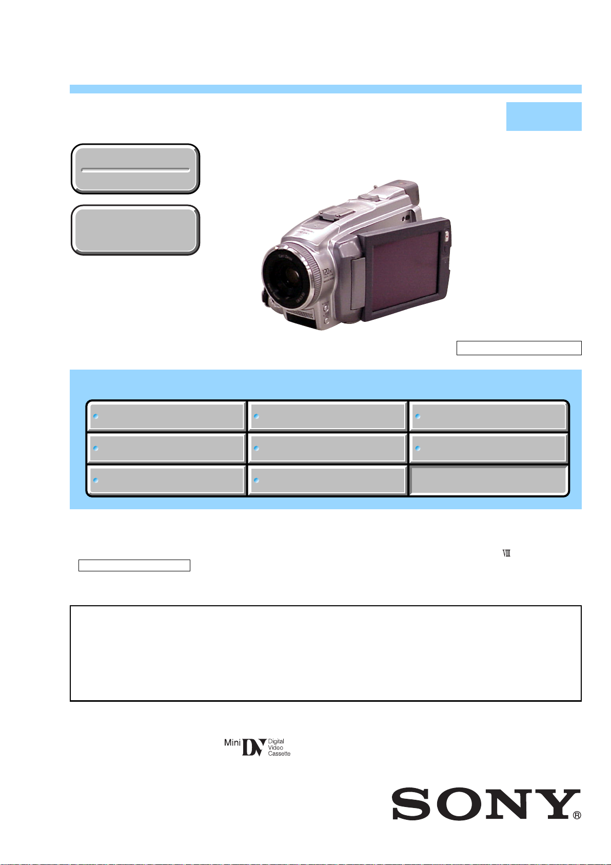
DCR-HC65
RMT-831
SERVICE MANUAL
Ver 1.0 2004. 03
Revision History
Revision History
How to use
How to use
Acrobat Reader
Acrobat Reader
Link
Link
SPECIFICATIONS
SPECIFICATIONS
BLOCK DIAGRAMS
BLOCK DIAGRAMS
LEVEL 2
DCR-HC65
US Model
Canadian Model
E Model
Korean Model
Z (Z200) MECHANISM
PRINTED WIRING BOARDS
PRINTED WIRING BOARDS
SERVICE NOTE
SERVICE NOTE
DISASSEMBLY
DISASSEMBLY
• For ADJUSTMENTS (SECTION 6), refer to SERVICE MANUAL, ADJ (987672851.pdf).
• For INSTR UCTION MANUAL, refer to SER VICE MANUAL, LEVEL 1 (987672841.pdf).
• For MECHANISM ADJUSTMENTS, refer to the “DV MECHANICAL ADJUSTMENT MANUAL
Z (Z200) MECHANISM ” (9-876-724-11) .
• Reference number search on printed wiring boards is available.
• TO TAKE OUT A CASSETTE WHEN NOT EJECT (FORCE EJECT)
On the VC-359 board
This service manual provides the information that is premised the circuit board replacement service and not intended repair
inside the VC-359 board.
Therefore, schematic diagram, printed wiring board, waveforms, mounted parts location and electrical parts list of the VC-359
board are not shown.
The following pages are not shown.
Schematic diagram .............................Pages 4-27 to 4-68
Printed wiring board............................Pages 4-93 to 4-96
FRAME SCHEMATIC DIAGRAMS
FRAME SCHEMATIC DIAGRAMS
SCHEMATIC DIAGRAMS
SCHEMATIC DIAGRAMS
Mounted parts location .............................
Electrical parts list...................................
REPAIR PARTS LIST
REPAIR PARTS LIST
Pages 4-99 to 4-100
Pages 5-19 to 5-27
DIGITAL VIDEO CAMERA RECORDER
Page 2

DCR-HC65
Video camera recorder
System
Video recording system
2 rotary heads, Helical scanning system
Still image recording system
Exif Ver. 2.2 *1
*1 “Exif” is a file format for still images,
established by the JEITA (Japan Electro n ic s
and Information Technology Industries
Association). Files in this format can have
additional information such as your
camcorder’s setting information at the time of
recording.
Audio recording system
Rotary heads, PCM system
Quantization: 12 bits (Fs 32 kHz, stereo 1,
stereo 2), 16 bits (Fs 48 kHz, stereo)
Video signal
NTSC color, EIA standards
Usable cassette
Mini DV cassette with the mark
printed
Tape speed
SP: Approx. 18.81 mm/s
LP: Approx. 12.56 mm/s
Recording/playback time (using a DVM60
cassette)
SP: 60 min
LP: 90 min
Fast forward/rewind time (using a DVM60
cassette)
Approx. 2 min 40 sec
Viewfinder
Electric viewfinder (color)
Image device
3.6 mm (1/5 type) CCD (Charge Coupled
Device)
Gross: Approx. 1 070 000 pixels
Effective (still): Ap prox. 1 000 000 pixels
Effective (movie): Approx. 690 000 pixels
Lens
Carl Zeiss Vario-Tessar
Combined power zoom lens
Filter diameter: 30 mm (1 3/16 in.)
10 × (Optical), 120 × (Digital)
F = 1.8 ~ 2.3
Focal length
3.2 - 32 mm (5/32 - 1 5/16 in.)
When converted to a 35 mm still camera
In CAMERA-TAPE:
46 - 460 mm (1 13/16 - 18 1/8 in.)
In CAMERA-MEMORY:
38 - 380 mm (1 1/2 - 15 in.)
SPECIFICATIONS
Color temperature
[AUTO], [ONE PUSH], [INDOOR]
(3 200 K), [OUTDOOR] (5 800 K)
Minimum illumination
7 1x (lux) (F 1.8)
0 lx (lux) (during NightShot plus function)*
* Objects unable to be seen due to the dark can be
shot with infrared ligh ting.
Input/Output connectors
Audio/Video input/output
10-pin connector
Input/output auto switch
Video signal: 1 Vp-p, 75 Ω (ohms),
unbalanced
Luminance signal: 1 Vp-p, 75 Ω(ohms),
unbalanced
Chrominance signal: 0.286 Vp-p, 75 Ω
(ohms), unbalanced
Audio signal: 327 mV (at output impedance
more than 47 kΩ (kilohms)), Input impedance
more than 47 kΩ(kilohms), Output impedance
with less than 2.2 kΩ (kilohms)
DV input/output
4-pin connector
Headphone jack
Stereo minijack (Ø 3.5 mm)
LANC jack
Stereo mini-minijack (Ø 2.5 mm)
USB jack
mini-B
MIC jack
Minijack, 0.388 mV low impedance with DC
2.5 to 3.0 V, output impedance 6.8 kΩ
(kilohms) (Ø 3.5 mm), Stereo type
LCD screen
Picture
8.8 cm (3.5 type)
Total dot number
123 200 (560 × 220)
General
Power requirements
DC 7.2 V (battery pack)
DC 8.4 V (AC Adaptor)
Average power consumption (when using the
battery pack)
During camera recording using the viewfinder
2.7 W
During camera recording using the LCD
3.8 W
Operating temperature
0°C to 40° C (32°F to 104° F)
Storage temperature
-20°C to + 60°C (-4° F to + 140°F)
Dimensions (approx.)
68 × 89 × 172 mm (2 3/4 × 3 5/8 × 6 7/8 i n . )
(w/h/d)
Mass (approx.)
560 g (1 lb 3 oz) main unit only
650 g (1 lb 6 oz) including the NP-FP50
rechargeable battery pack and DVM60
cassette.
Supplied accessories
See page 5-14.
AC Adaptor AC-L25A/L25B
Power requirements
AC 100 - 240 V, 50/60 Hz
Current consumption
0.35 - 0.18 A
Power consumption
18 W
Output voltage
DC 8.4 V, 1.5 A
Operating te mp erature
0°C to 40°C (32°F to 104°F)
Storage temperature
-20°C to + 60° C (-4°F to + 140° F)
Dimensions (approx.)
56 × 31 × 100 mm (2 1/4 × 11/4 × 4 in.)
(w/h/d) excluding the projecting parts
Mass (approx.)
190 g (6.7 oz) excluding the power cord
Rechargeable battery pack (NP-FP50)
Maximum output voltage
DC 8.4 V
Output voltage
DC 7.2 V
Capacity
4.9 Wh (680 mAh)
Dimensions (approx.)
31.8 × 18.5 × 45.0 mm
(1 5/16 × 3/4 × 1 13/16 in.) (w/h/d)
Mass (approx.)
40 g (1.5 oz)
Operating te mp erature
0°C to 40°C (32°F to 104°F)
Type
Lithium ion
Design and specifications are
subject to change without notice.
— 2 —
Page 3

SAFETY CHECK-OUT
After correcting the original service problem, perform the following
safety checks before releasing the set to the customer.
DCR-HC65
1. Check the area of your repair for unsoldered or poorly-soldered
connections. Check the entire board surface for solder splashes
and bridges.
2. Check the interboard wiring to ensure that no wires are
"pinched" or contact high-wattage resistors.
3. Look for unauthorized replacement parts, particularly
transistors, that were installed during a previous repair . Point
them out to the customer and recommend their replacement.
4. Look for parts which, through functioning, show obvious signs
of deterioration. Point them out to the customer and
recommend their replacement.
5. Check the B+ voltage to see it is at the values specified.
6. Flexible Circuit Board Repairing
• Keep the temperature of the soldering iron around 270˚C
during repairing.
• Do not touch the soldering iron on the same conductor of the
circuit board (within 3 times).
• Be careful not to apply force on the conductor when soldering
or unsoldering.
SAFETY-RELATED COMPONENT WARNING!!
COMPONENTS IDENTIFIED BY MARK 0 OR DOTTED LINE WITH
MARK 0 ON THE SCHEMATIC DIAGRAMS AND IN THE PARTS
LIST ARE CRITICAL TO SAFE OPERATION. REPLACE THESE
COMPONENTS WITH SONY PARTS WHOSE PART NUMBERS
APPEAR AS SHOWN IN THIS MANUAL OR IN SUPPLEMENTS
PUBLISHED BY SONY .
Unleaded solder
Boards requiring use of unleaded solder are printed with the leadfree mark (LF) indicating the solder contains no lead.
(Caution: Some printed circuit boards may not come printed with
the lead free mark due to their particular size.)
: LEAD FREE MARK
Unleaded solder has the following characteristics.
• Unleaded solder melts at a temperature about 40°C higher than
ordinary solder.
Ordinary soldering irons can be used but the iron tip has to be
applied to the solder joint for a slightly longer time.
Soldering irons using a temperature regulator should be set to
about 350°C.
Caution: The printed pattern (copper foil) may peel away if the
heated tip is applied for too long, so be careful!
• Strong viscosity
Unleaded solder is more viscous (sticky , less prone to flow) than
ordinary solder so use caution not to let solder bridges occur such
as on IC pins, etc.
• Usable with ordinary solder
It is best to use only unleaded solder but unleaded solder may
also be added to ordinary solder.
ATTENTION AU COMPOSANT AYANT RAPPORT
À LA SÉCURITÉ!
LES COMPOSANTS IDENTIFÉS P AR UNE MARQUE 0 SUR LES
DIAGRAMMES SCHÉMA TIQUES ET LA LISTE DES PIÈCES SONT
CRITIQUES POUR LA SÉCURITÉ DE FONCTIONNEMENT. NE
REMPLACER CES COMPOSANTS QUE PAR DES PIÈSES SONY
DONT LES NUMÉROS SONT DONNÉS DANS CE MANUEL OU
DANS LES SUPPÉMENTS PUBLIÉS PAR SONY.
CAUTION :
Danger of explosion if battery is incorrectly replaced.
Replace only with the same or equivalent type.
— 3 —
Page 4

DCR-HC65
TABLE OF CONTENTS
1. SERVICE NOTE
1-1. SER VICE NOTE ····························································· 1-1
1. NOTE FOR REPAIR ······················································· 1-1
2. POWER SUPPLY DURING REPAIRS ··························1-2
3. TO TAKE OUT A CASSETTE WHEN NOT EJECT
(FORCE EJECT) ·····························································1-2
1-2. SELF-DIAGNOSIS FUNCTION····································1-3
1. SELF-DIAGNOSIS FUNCTION····································1-3
2. SELF-DIAGNOSIS DISPLAY ·······································1-3
3. SELF-DIAGNOSIS CODE TABLE ································1-4
2. DISASSEMBLY
2-1. DISASSEMBLY······························································2-1
2-2. SERVICE POSITION ·····················································2-3
2-3. CIRCUIT BOARDS LOCATION ··································· 2-5
2-4. FLEXIBLE BOARDS LOCATION ································2-6
HELP (List of caution points is shown here.)
3. BLOCK DIAGRAMS
3-1. OVERALL BLOCK DIAGRAM (1/4) ···························3-1
3-2. OVERALL BLOCK DIAGRAM (2/4) ···························3-3
3-3. OVERALL BLOCK DIAGRAM (3/4) ···························3-5
3-4. OVERALL BLOCK DIAGRAM (4/4) ···························3-7
3-5. POWER BLOCK DIAGRAM (1/2)································3-9
3-6. POWER BLOCK DIAGRAM (2/2)······························3-11
4. PRINTED WIRING BOARDS AND
SCHEMATIC DIAGRAMS
4-1. FRAME SCHEMATIC DIAGRAM (1/2)·······················4-1
FRAME SCHEMATIC DIAGRAM (2/2)·······················4-3
4-2. SCHEMATIC DIAGRAMS
• CD-513 (CCD IMAGER)
SCHEMATIC DIAGRAM············································4-7
• CK-141 (RELAY, FUNCTION KEY)
SCHEMATIC DIAGRAM············································4-9
• FP-911 FLEXIBLE
SCHEMATIC DIAGRAM··········································4-10
• JK-268 (JACK)
SCHEMATIC DIAGRAM··········································4-11
• JM-016 (JACK-2)
SCHEMATIC DIAGRAM··········································4-11
• PD-219 (RGB DRIVE, TIMING GENERATOR)
SCHEMATIC DIAGRAM··········································4-13
• CONTROL KEY BLOCK (SB7800)
SCHEMATIC DIAGRAM··········································4-13
• LB-102 (EVF BACK LIGHT)
SCHEMATIC DIAGRAM··········································4-15
• MS-210 (MS CONNECTOR)
SCHEMATIC DIAGRAM··········································4-15
• MI-051 (INDICATOR, IR SENSOR)
SCHEMATIC DIAGRAM··········································4-17
• FS-087 (MF PHOTO SENSOR)
SCHEMATIC DIAGRAM··········································4-17
• FP-909 FLEXIBLE
SCHEMATIC DIAGRAM··········································4-17
• SL-064 (FUNCTION KEY)
SCHEMATIC DIAGRAM··········································4-19
• FP-912 FLEXIBLE
SCHEMATIC DIAGRAM··········································4-19
• FP-910 FLEXIBLE
SCHEMATIC DIAGRAM··········································4-20
• CONTROL KEY BLOCK (PS7800)
SCHEMATIC DIAGRAM··········································4-21
• CONTROL KEY BLOCK (FK7800)
SCHEMATIC DIAGRAM··········································4-21
• FP-228/467/826 FLEXIBLE
(S/T REEL SENSOR, TAPE SENSOR)
SCHEMATIC DIAGRAM··········································4-23
Shematic diagram of the VC-359 board is not shown.
Pages from 4-27 to 4-68 are not shown.
4-3. PRINTED WIRING BOARDS
• CD-513 (CCD IMAGER) (-11) (-12)
PRINTED WIRING BOARD ·····································4-73
• CK-141 (RELAY, FUNCTION KEY) (-11)
PRINTED WIRING BOARD ·····································4-75
• CK-141 (RELAY, FUNCTION KEY) (-12)
PRINTED WIRING BOARD ·····································4-77
• FS-087 (MF PHOTO SENSOR)
PRINTED WIRING BOARD ·····································4-79
• JK-268 (JACK)
PRINTED WIRING BOARD ·····································4-79
• JM-016 (JACK-2) (-11) (-12)
PRINTED WIRING BOARD ·····································4-81
• MI-051 (INDICATOR, IR SENSOR)
PRINTED WIRING BOARD ·····································4-83
• SL-064 (FUNCTION KEY)
PRINTED WIRING BOARD ·····································4-83
• MS-210 (MS CONNECTOR) (-11) (-12)
PRINTED WIRING BOARD ·····································4-85
• PD-219(RGB DRIVE, TIMING GENERATOR)
PRINTED WIRING BOARD ·····································4-87
• FP-228/467/826 FLEXIBLE
(S/T REEL SENSOR, TAPE SENSOR)
PRINTED WIRING BOARD ·····································4-89
• LB-102 (EVF BACK LIGHT)
PRINTED WIRING BOARD ·····································4-89
Printed wiring board of the VC-359 board is not shown.
Pages from 4-93 to 4-96 are not shown.
4-4. MOUNTED PARTS LOCATION ·································4-97
Mounted parts location of the
Pages from 4-99 to 4-100 are not shown.
VC-359
board is not shown.
5. REPAIR PARTS LIST
5-1. EXPLODED VIEWS ······················································5-3
5-1-1.OVERALL SECTION·····················································5-3
5-1-2.CABINET (R) SECTION ···············································5-4
5-1-3.LCD SECTION ·······························································5-5
5-1-4.CABINET (L) SECTION-1 ············································5-6
5-1-5.CABINET (L) SECTION-2 ············································5-7
5-1-6.MAIN CHASSIS SECTION ···········································5-8
5-1-7.EVF SECTION································································5-9
5-1-8.LENS SECTION ··························································· 5-10
5-1-9.MECHANISM DECK OVERALL (Z200) ···················5-11
5-1-10. LS CHASSIS BLOCK ASSEMBLY ··························5-12
5-1-11. MECHANICAL CHASSIS BLOCK ASSEMBLY ····5-13
Other accessories ···························································5-14
5-2. ELECTRICAL PARTS LIST ········································ 5-15
Electrical parts list of the VC-359 board is not shown.
Pages from 5-19 to 5-27 are not shown.
— 4 —
Page 5
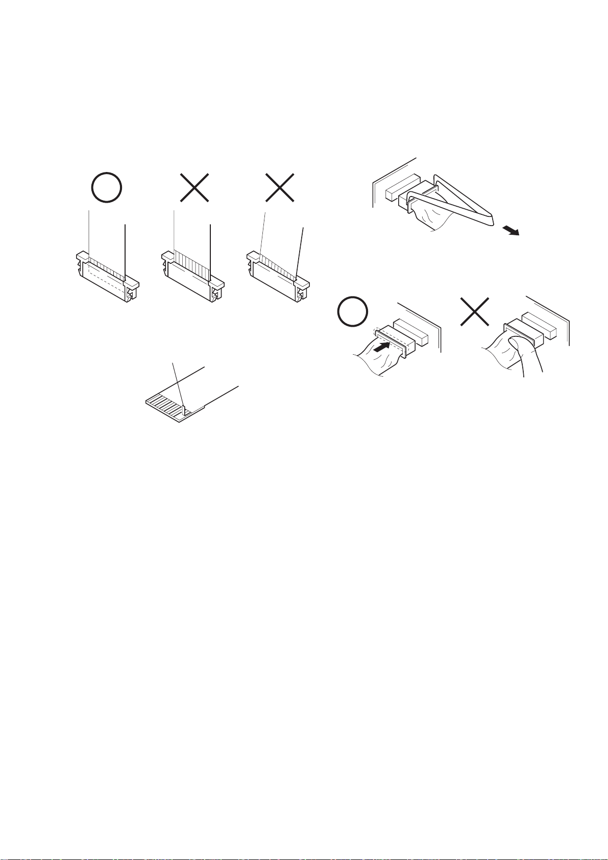
Make sure that the flat cable and flexible board are not cracked of
bent at the terminal.
Do not insert the cable insufficiently nor crookedly.
Cut and remove the part of gilt
which comes off at the point.
(Take care that there are
some pieces of gilt left inside)
When remove a connector, don't pull at wire of connector.
Be in danger of the snapping of a wire.
When installing a connector, don't press down at wire of connector.
Be in danger of the snapping of a wire.
1-1. SER VICE NOTE
1. NOTE FOR REPAIR
DCR-HC65
SECTION 1
SERVICE NOTE
1-1
Page 6
DCR-HC65
)
2. POWER SUPPLY DURING REPAIRS
In this unit, about 10 seconds after power is supplied to the battery terminal using the regulated po wer supply (8.4V), the power is shut of f so
that the unit cannot operate.
This following two methods are available to prevent this. Take note of which to use during repairs.
Method 1.
Use the AC power adaptor (AC-L25).
Method 2.
Connect the servicing remote commander RM-95 (J-6082-053-B) to the LANC jack, and set the commander switch to the “ADJ” side.
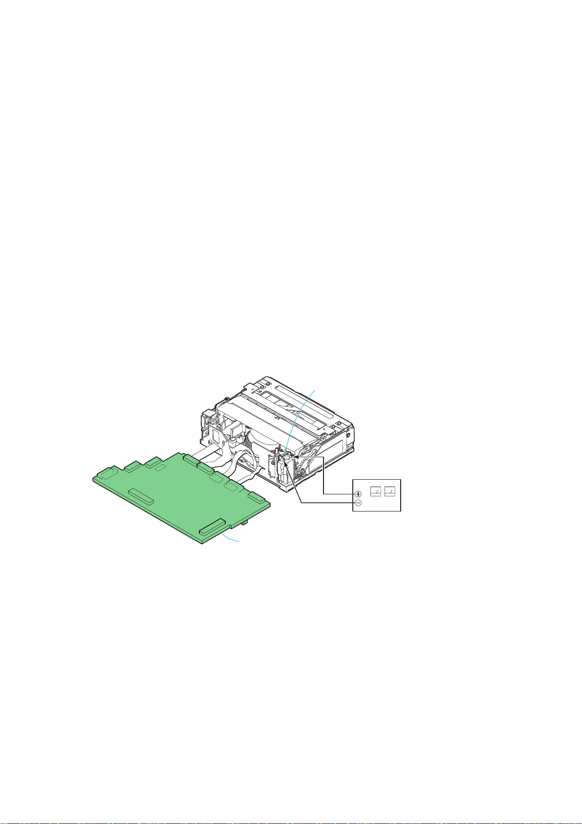
3. TO TAKE OUT A CASSETTE WHEN NOT EJECT (FORCE EJECT)
1 Open the flash.
2 Remove the cabinet (F) section.
3 Remove the cabinet (R) section.
4 Remove the EVF section.
5 Remove the VC-359 board.
6 Remove the mechanism deck.
7 Supply +4.5V from the DC power supply to the loading motor and unload with pressing the cassette compartment.
VC-359
Loading motor
DC power supply (+4.5Vdc
VC-359 board
1-2
Page 7
1-2. SELF-DIA GNOSIS FUNCTION
1. SELF-DIAGNOSIS FUNCTION
When problems occur while the unit is operating, the self-diagnosis
function starts working, and displays on the viewfinder, or LCD
screen what to do. This function consists of two display; selfdiagnosis display and service mode display.
Details of the self-diagnosis functions are provided in the Instruction
manual.
Viewfinder or LCD screen
C : 3 1 : 1 1
Blinks at 3.2Hz
DCR-HC65
2. SELF-DIAGNOSIS DISPLAY
When problems occur while the unit is operating, the counter of the
viewfinder or LCD screen consists of an alphabet and 4-digit number ,
which blinks at 3.2Hz. This 5-character display indicates the
“repaired by:”, “block” in which the problem occurred, and “detailed
code” of the problem.
3 1C
Repaired by:
C : Corrected by customer
H : Corrected by dealer
E : Corrected by service
engineer
Note: The “self-diagnosis display” data will be kept even if the lithium battery (BT151 of CK-141 board) is removed.
Indicates the appropriate
step to be taken.
E.g.
31 ....Reload the tape.
32 ....Turn on power again.
Block
1 1
Detailed Code
Refer to page 1-4.
Self-diagnosis Code Table.
1-3
Page 8

DCR-HC65
3. SELF-DIAGNOSIS CODE TABLE
Self-diagnosis Code
Function
Repaired by:
C
C
C
C
C
C
C
C
C
C
C
C
C
C
C
C
C
C
C
C
C
C
C
E
E
E
E
E
Block
04
21
22
31
31
31
31
31
31
31
31
31
31
31
31
32
32
32
32
32
32
32
32
20
61
61
62
62
Detailed
Code
00
00
00
10
11
20
21
22
23
24
30
40
42
10
11
20
21
22
23
24
30
40
42
00
00
10
00
01
Symptom/State
Non-standard battery is used.
Condensation.
Video head is dirty.
LOAD direction. Loading does not
complete within specified time
UNLOAD direction. Loading does not
complete within specified time
T reel side tape slacking when unloading
Winding S reel fault when counting the
rest of tape.
T reel fault.
S reel fault.
T reel fault.
FG fault when starting capstan.
FG fault when starting drum.
FG fault during normal drum operations.
LOAD direction loading motor time-
out.
UNLOAD direction loading motor
time-out.
T reel side tape slacking when
unloading.
Winding S reel fault when counting the
rest of tape.
T reel fault.
S reel fault.
T reel fault.
FG fault when starting capstan.
FG fault when starting drum
FG fault during normal drum
operations
Data on A page or D page are rewriten.
Difficult to adjust focus
(Cannot initialize focus.)
Zoom operations fault
(Cannot initialize zoom lens.)
Steadyshot function does not work well.
(With pitch angular velocity sensor output
stopped.)
Steadyshot function does not work well.
(With yaw angular velocity sensor output
stopped.)
Correction
Use the info LITHIUM battery.
Remove the cassette, and insert it again after one hour.
Clean with the optional cleaning cassette.
Load the tape again, and perform operations from the beginning.
Load the tape again, and perform operations from the beginning.
.
Load the tape again, and perform operations from the beginning.
Load the tape again, and perform operations from the beginning.
Load the tape again, and perform operations from the beginning.
Load the tape again, and perform operations from the beginning.
Load the tape again, and perform operations from the beginning.
Load the tape again, and perform operations from the beginning.
Load the tape again, and perform operations from the beginning.
Load the tape again, and perform operations from the beginning.
Remove the battery or power cable, connect, and perform
operations from the beginning.
Remove the battery or power cable, connect, and perform
operations from the beginning.
Remove the battery or power cable, connect, and perform
operations from the beginning.
Remove the battery or power cable, connect, and perform
operations from the beginning.
Remove the battery or power cable, connect, and perform
operations from the beginning.
Remove the battery or power cable, connect, and perform
operations from the beginning.
Remove the battery or power cable, connect, and perform
operations from the beginning.
Remove the battery or power cable, connect, and perform
operations from the beginning.
Remove the battery or power cable, connect, and perform
operations from the beginning.
Remove the battery or power cable, connect, and perform
operations from the beginning.
Make data on A page and D page correct value.
Inspect the lens block focus MR sensor (Pin 1, 2 of CN5101 of
VC-359 board) when focusing is performed when the focus ring is
rotated in the focus manual mode, and the focus motor drive circuit
(IC5101 of VC-359 board) when the focusing is not performed.
Inspect the lens block zoom reset sensor (
VC-359 board
is operated and the zoom motor drive circuit (IC5101 of VC-359
board) when zooming is not performed.
Inspect pitch angular velocity sensor (SE401 of CD-513 board)
peripheral circuits.
Inspect yaw angular velocity sensor (SE402 of CD-513 board)
peripheral circuits.
) when zooming is performed when the zoom switch
Pin wh of CN5101 of
1-4E
Page 9
SECTION 2
)
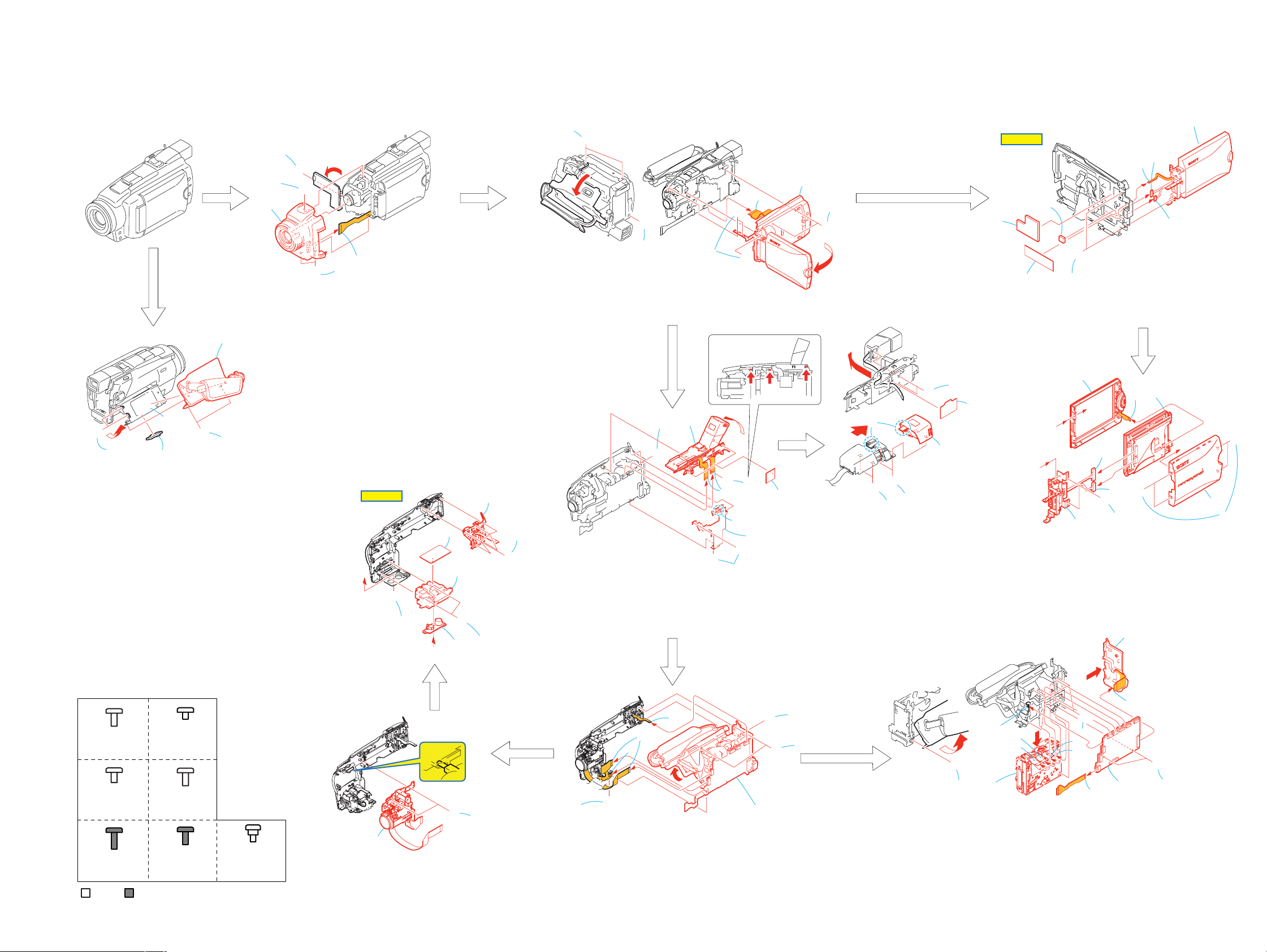
DISASSEMBLY
The following flow chart shows the disassembly procedure.
2-1. DISASSEMBLY
3
A
1
6
6
2
A
A
DCR-HC65
2
A
1
7
B
A
1
Screw (M1.7x4) silver
5
2
4
Open the jack cover assembly.
3
Screw (M1.7x4) silver
4
Two screws (M1.7x4) silver
5
FP-919 flexible board (28P)
6
Cabinet (F) section
1
Open the cassette lid.
2
Two screws (M1.7x4) silver
3
Screw (M1.7x4) silver
4
Three screws (M1.7x2.5) silver
3
5
6
7
8
4
B
Open the LCD panel.
Two screws (M1.7x4) silver
FP-920 flexible board (51P)
Cabinet (R) section
8
6
A
5
1
HELP 01
2
1
2
3
3
D
7
Tape (R), fixed
Tape (CK), fixed
Spacer (R), fixed
5
6
4
Harness (PC-131) (10P)
5
Harness (PC-132) (14P)
6
FP-911 flexible board (6P)
7
Two screws (M1.7x4) silver
8
LCD section
8
4
B
4
B
1
2
1
Open the cassette lid.
2
Two screws (M1.7x2.5) silver
3
Two screws (M1.7x2.5) silver
4
Screw (M1.7x2.5) silver
5
Eject knob
6
Cabinet (G) section
A
Screw
M1.7x4
3-078-893-21
C
Tapping screw
M1.7x3.5
3-078-890-01
E
Tapping screw
M1.7x5
3-080-222-21
Silver
5
B
3-989-735-01
D
3-055-573-21
FG
Tapping screw
3-080-222-11
Black
Screw
M1.7x2.5
Screw
M1.7x4
M1.7x4
B
3
Special screw
1.4x1.5
3-062-214-01
1
Screw (M1.7x4) silver
2
Shield sheet (JK)
3
Two tapping screw
(M1.7x3.5) silver
4
Screw
5
JM-016 board,
JK-268 board,
FP-918 flexible board, etc.
6
Five tapping screws
(M1.7x3.5) silver
7
Control key block (PS7800),
ST bracket (front)
a
1
Two tapping screws (M1.7x3.5) silver
2
Lens section
HELP 02
2
A
A
3
9
1
7
a
7
5
E
2
1
8
8
9
7
b
a
4
a
A
b
C
8
7
2
5
1
C
3
4
a
C
1
C
6
1
Screw (M1.7x4) silver
2
Two screws (M1.7x2.5) silver
3
Craw
4
VC radiation plate assembly
5
Harness fixed tape
6
FP-916 flexible board (21P),
Control key block(FK7800)(14P)
2
1
7
6
A
3
1
FP-913 flexible board (33P),
Flexible board (from lensdevice)(29P)
2
Control key block(PS7800)(10P)
3
Screw (M1.7x4) silver
4
Screw (M1.7x4) silver
5
Two screws (M1.7x2.5) silver
6
3
B
B
2
7
Raise the Finder
8
Three tapping screws
(M1.7x3.5) silver
9
EVF section
VC-359
6
Open the cassette lid.
7
FP-918 flexible board (27P)
8
VC-359 board, Mechanism deck,
Cabinet (G) section, etc.
5
1
VF shield sheet
2
4
4
A
B
8
Two tapping screws (M1.7x5) black
3
Remove the EVF block .
4
Two tapping screws (M1.7x5) black
5
Pull out the VF lens assembly in the
direction of the arrow a.
6
Two tapping screws (M1.7x4) black
7
Remove the craw.
8
VF lens assembly.
5
E
4
F
6
1
A
2
1
Open the cassette lid.
2
Screw (M1.7x4) silver
3
FP-912 flexible board (30P)
4
Battery panel section
5
Flexible board (CN9102) (27P)
6
Flexible board (CN9103) (27P)
7
FP-919 flexible board (27P)
1
Four screws (M1.7x4) silver
2
P cabinet (C) assembly (841)
3
Harness (PC-131) (10P)
4
Harness (PC-132) (14P)
5
Two screws (M1.7x2.5) silver
8
5
6
qf
8
FP-910 flexible board (6P)
9
Two screws (M1.7x2.5) silver
q;
Flexible board (CN9101) (10P)
qa
Flexible board (CN6501) (10P)
qs
VC-359 board
qd
Four screws (M1.4x1.5) silver
qf
Mechanism deck
3
B
6
A
5
6
Hinge section
7
Control key block (SB7800) (6P
8
P cabinet (M) assembly
9
PD-219 board,
LCD unit (ACX531AKM-J),
Light guide plate block
4
3
2
1
G
qd
q;
qa
VC-359
B
qs
7
9
2-1 2-2
Page 10
DCR-HC65
2-2. SERVICE POSITION
2. DISASSEMBLY
2. DISASSEMBLY
3
A
1
6
A
A
2
5
4
2
A
2
7
6
C
a
1
5
[SERVICE POSITION TO CHECK THE VTR SECTION]
Connection to Check the VTR Section
To check the VTR section, set the VTR to the "Forced VTR power ON" mode.
Operate the VTR functions using the adjustment remote commander (with the HOLD switch set in the OFF position.)
Setting the "Forced VTR Power ON" mode
1) Select page: 0, address: 01, and set data: 01.
2) Select page: 0, address: 10, and set data: 00.
3) Select page: A, address: 10, set data: 02, and press the
PAUSE button of the adjustment remote commander.
Exiting the "Forced VTR Power ON" mode
1) Select page: 0, address: 01, and set data: 01.
2) Select page: 0, address: 10, and set data: 00.
3) Select page: A, address: 10, set data: 00, and press the
PAUSE button of the adjustment remote commander.
4) Select page: 0, address: 01, and set data: 00.
Monitor TV
Mechanism deck
A
A
1
8
7
B
3
6
A
4
B
5
9
1
7
2
A
C
3
4
a
C
1
JM-016 board
A/V
JK-268 board
LANC
FP-918 Flexible
board (27P)
VC-359 board
CN1201
CN9103
CN9102
CN9101
VC-359
CN2101
CN6501
CN1207
FP-912 Flexible
board (30P)
CPC-15
(J-6082-564-A)
1
8
C
8
6
3
B
B
2
2
1
7
VC-359
6
A
3
5
A
1
4
2
3
4
4
A
Adjustment remote
commander (RM-95)
CN1205
To eject the cassette, short-circuit between
3
and pin 1 (GND) of CN1205 on
pin
the VC-359 board for 1 second.
1
3
Battery panel section
I/F unit for LANC control
(J-6082-521-A)
DC-IN
G
5
B
8
8
5
6
qd
q;
qa
VC-359
AC power
adaptor
AC IN
B
qf
qs
7
9
2-3 2-4
Page 11
2. DISASSEMBLY
CCD IMAGER
RELAY, FUNCTION KEY
MF PHOTO SENSOR
JACK
JACK-2
EVF BACK LIGHT
INDICATOR, IR SENSOR
MS CONNECTOR
RGB DRIVE, TIMING GENERATOR
FUNCTION KEY
TIMING GENERATOR, S/H, AGC, A/D CONV., LENS DRIVE, CAMERA PROCESS, MPEG
MOVIE/DIGITAL STILL PROCESS, 64Mbit SDRAM, BUFFER, HI/DIGITAL STILL CONTROL,
32Mbit FLASH, 16Mbit SDRAM, DV SIGNAL PROCESS, DV INTERFACE, REC/PB AMP,
VIDEO I/O, DRUM/CAPSTAN/LOADING DRIVE, CAMERA/MECHA CONTROL, HI CONTROL,
EVF VIDEO, AUDIO I/O, MIC AMP, DC IN, CHARGE, DC/DC CONVERTER, CONNECTOR
CD-513
CK-141
FS-087
JK-268
JM-016
LB-102
MI-051
MS-210
PD-219
SL-064
NAME
FUNCTION
CD-513
LB-102
PD-219
SL-064
CK-141
VC-359
VC-359
MS-210
JM-016
MI-051
FS-087
JK-268
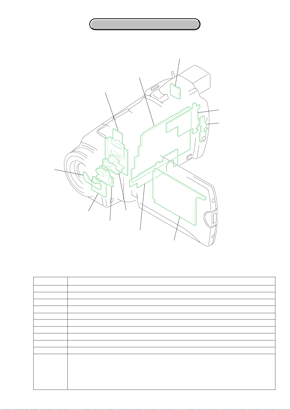
2. DISASSEMBLY
2-3. CIRCUIT BOARDS LOCATION
DCR-HC65
2-5
Page 12
DCR-HC65
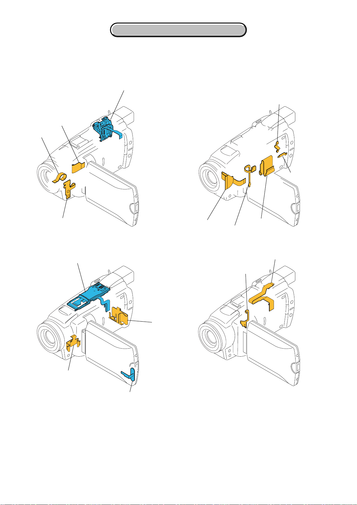
3
2-4. FLEXIBLE BOARDS LOCATION
The flexible boards contained in the lens block is not shown.
CONTROL KEY BLOCK
(PS7800)
FP-913
FP-922
2. DISASSEMBLY
2. DISASSEMBLY
FP-921
FP-92
FP-909
CONTROL KEY BLOCK
(FK7800)
FP-918
FP-912
FP-919
FP-911
FP-910
FP-920
FP-916
CONTROL KEY BLOCK
(SB7800)
2-6E
Page 13
DCR-HC65
r
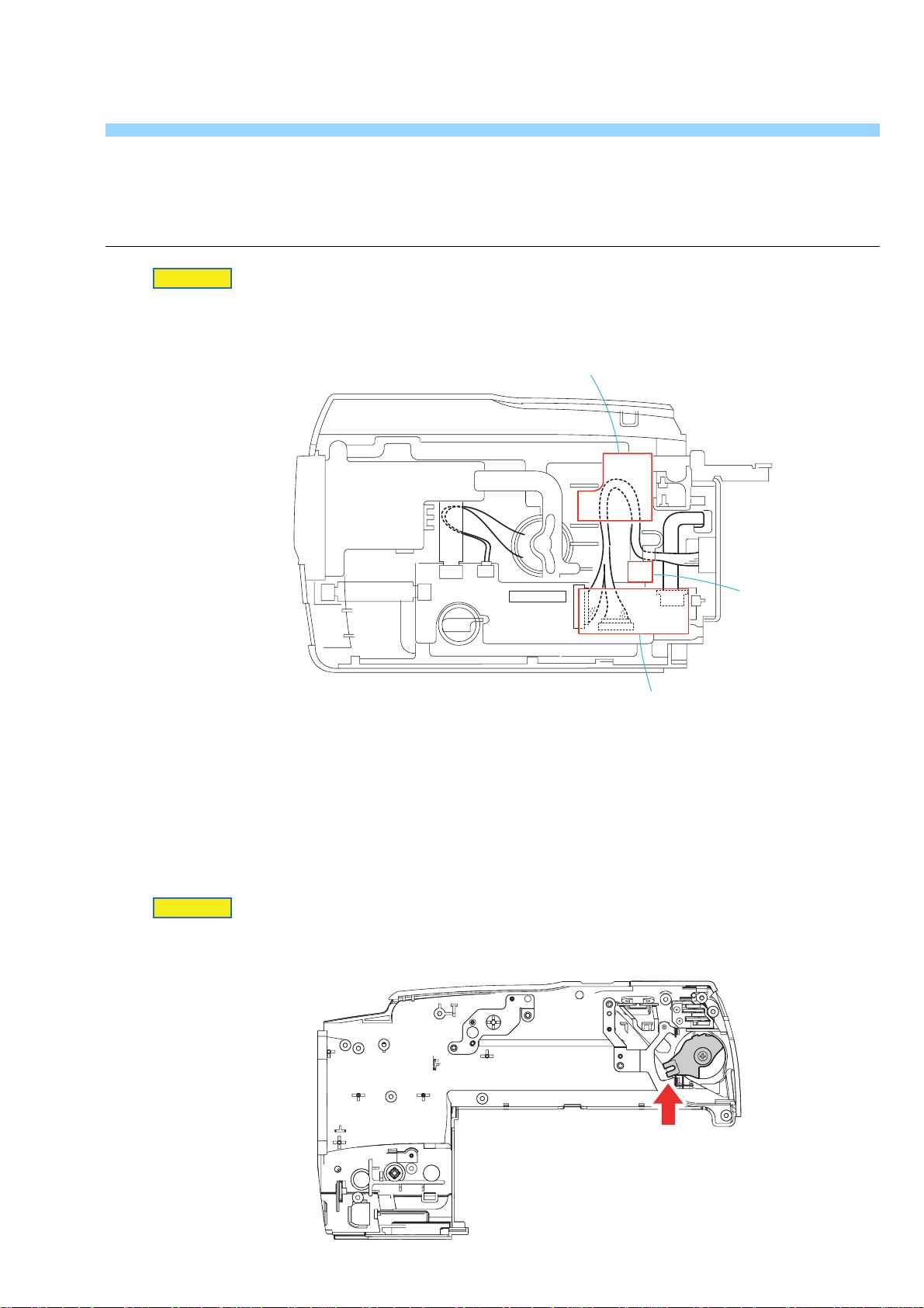
HELP
Sheet attachment positions and procedures of processing the flexible boards/harnesses are shown.
HELP 01
Fixed (R) tape
HELP 02
Fixed (R) space
Fixed (CK) tape
Alignment position
HELP
Page 14
Link
Link
DCR-HC65
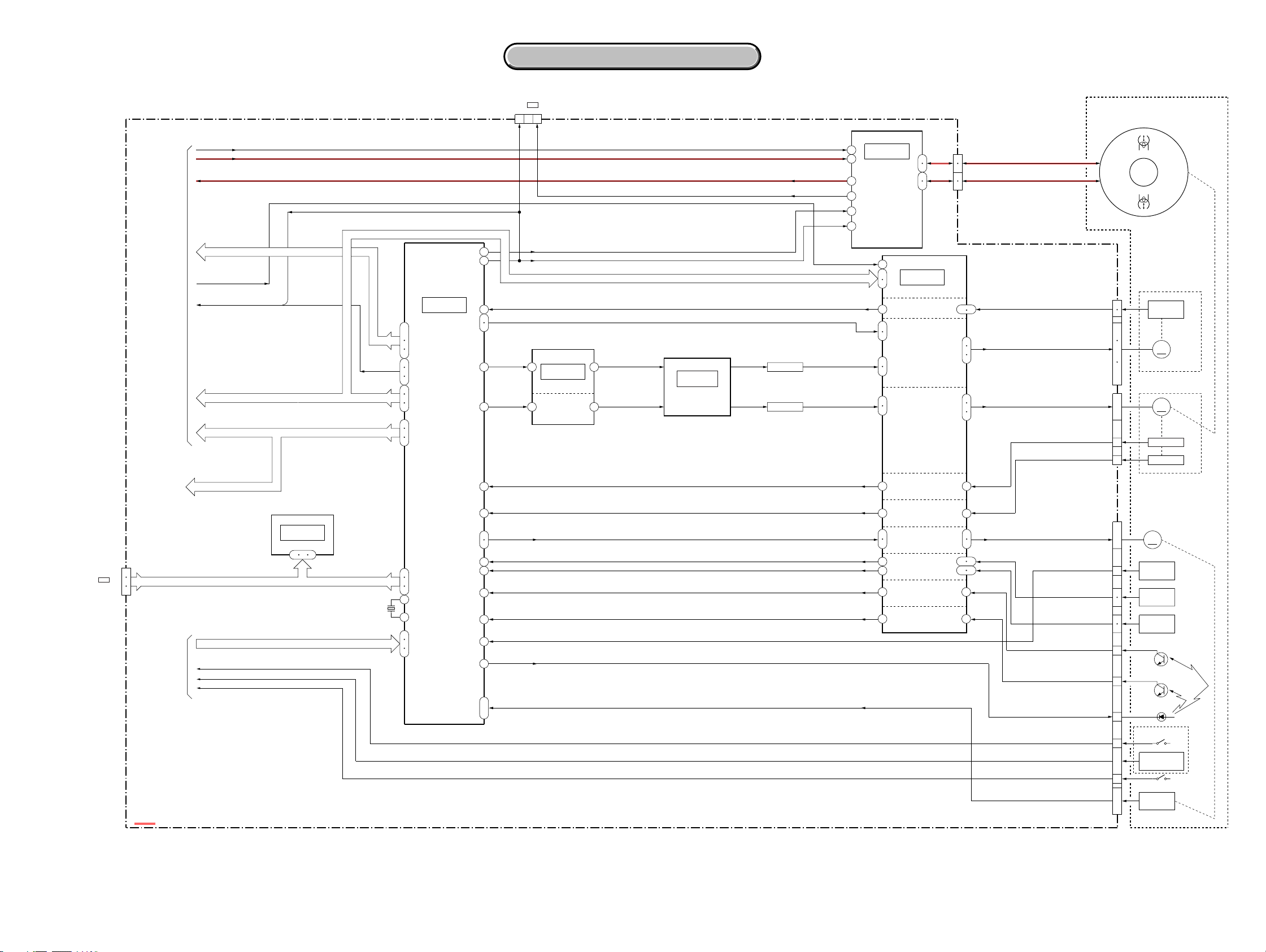
3. BLOCK DIAGRAMS
OVERALL BLOCK DIAGRAM (1/4)
OVERALL BLOCK DIAGRAM (1/4)
OVERALL BLOCK DIAGRAM (2/4) POWER BLOCK DIAGRAM (2/2)
OVERALL BLOCK DIAGRAM (2/4) POWER BLOCK DIAGRAM (2/2)
OVERALL BLOCK DIAGRAM (3/4)
OVERALL BLOCK DIAGRAM (3/4)
OVERALL BLOCK DIAGRAM (4/4)
OVERALL BLOCK DIAGRAM (4/4)
POWER BLOCK DIAGRAM (1/2)
POWER BLOCK DIAGRAM (1/2)
Page 15
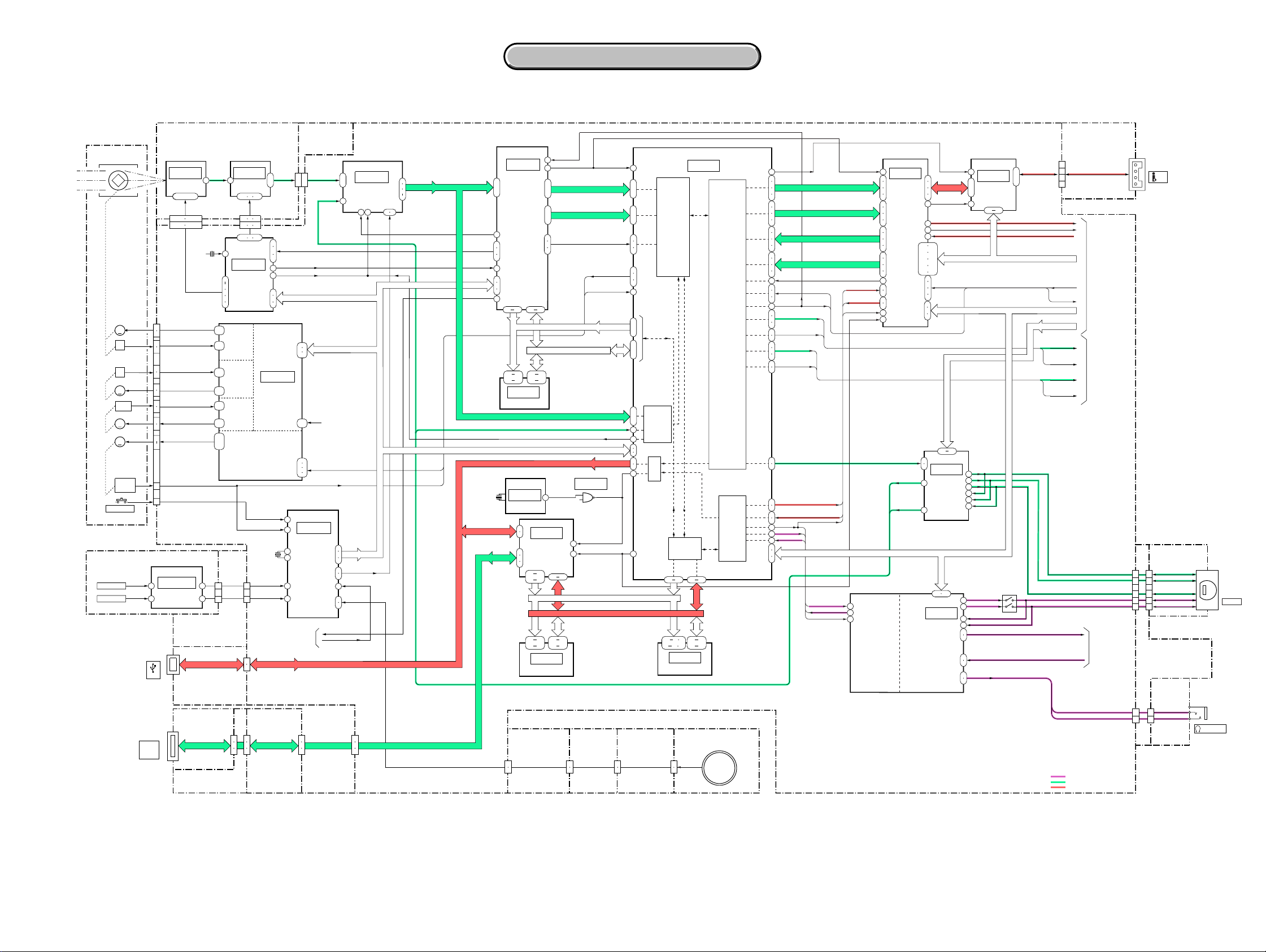
DCR-HC65
BLOCK DIAGRAMS
3-1. OVERALL BLOCK DIAGRAM (1/4)
LENS ASSY
IRIS
(SHUTTER)
M
H
H
ND FILTER
METER
M
MR
FOCUS
M
MOTOR
M
ZOOM
MOTOR
ZOOM
RESET
SENSOR
NIGHT SHOT
CD-513 BOARD (2/2)
SE402
YAW SENSOR
SE401
PITCH SENSOR
CN702
MEMORY
STICK
CONNECTOR
CD-513 BOARD (1/2)
IC201
12
CCD
IMAGER
4-1 14 16 18
•••
V1-V4
RG,H1,H2
CN201
30-33
11-13
4-1
23-21
CN5001
X5001
66MHz
IRIS DRIVE
23
+,-
22
IRIS HALL
+,-
21
25
ND HALL
17
+,-
15
ND DRIVE
12
+,-
13
2
FMR A,B
1
10
FOCUS +,-
11
6
ZOOM A,XA,B,XB
9
ZOOM RST ZOOM RST
26
XNS SW
18
CN5101
IC401
12
8
YAW/PITCH
SENSOR
AMP
18
2
IC202
5
S/H
13 14 1
XSHD,XSHP,CLPDM
15 16 24
19 18 10
38 33 64
(1/21)
CN201
CN5001
•
4
11
47
IC5001
TIMING
67
GENERATOR
72
32
17
25
H1
J1
IRIS
DRIVE
C5
B6
ZOOM MOTOR
30
28
CN5001
DRIVE
IC5101
X8801
20MHz
YAW AD
PITCH AD
(2/21)
C10
ND
B11
FILTER
DRIVE
K2
L2
B1
C4
FOCUS
MOTOR
DRIVE
F3
E3
K6
L4
F1
G3
4
6
CN201
FP-913
USB D+,D-
(2/2)
CN2101
10
USB D+,D-
8
(FLEXIBLE)
CN001
(USB)
FP-912
(FLEXIBLE)
(1/3)
MS-210
BOARD(1/2)
Duo
MS BS,DIO,SCLK MS BS,DIO,SCLK
CN156
6
6
5
5
3
3
CN701
CK-141
FP-921
(FLEXIBLE)
16
(1/2)
BOARD
(1/3)
FP-913
(FLEXIBLE)
(1/2)
CCD OUT
14
20
+,-
••
16
18
CN5001CN201
IC1701 Y OUT
9
HD,VD,FLD HD,VD,FLD
10
12
CHCK CHCK
53
ADCK27
59
5
CAM SO,SI,SCK
2
1
J11
K11
H12
K12
SPCK
(IC6201)
EN1
K9
DIR1A
L9
DIR1B
M9
J9
(13/21)
187
IC8801
54
CAMERA CONTROL
1
3
130
129
TO
OVERALL
1
BLOCK DIAGRAM
(4/4)
(PAGE 3-8)
CN151
10
9
7
FP-920
(FLEXIBLE)
(1/3)
SECTION 3
3. BLOCK DIAGRAMS
3. BLOCK DIAGRAMS
( ) : Number in parenthesis ( ) indicates the division number of schematic diagram where the component is located.
VC-359 BOARD(1/4)
(1/2)
EXT STROBO
ZOOM VR AD
77
78
75
73
71
135
210
211
30
•
31
34
CAM SO,SI,SCK
CH SO,SCK
MF A
MF B
IC5003
20
CN1203
42
43
45
(1/21)
AGC
A/D CONV.
16
44 45
CH SO,SCK
IC7101 Y OUT
(3/21)
IC5201
CAMERA
47
48
AD0-AD13
AD0-AD13
1
12
AD0-AD13
EXT STROBO
PROCESS
56
|
71
CLPOB
77
92
91
90
137
22
23
20
102
195 174
161 144
A0-A10, A12
26
20
35
29
IC6202
64Mbit
SDRAM
(7/21)
X8401
IC8403
48MHz
USB D+,D-
MS BS,DIO,SCLK
MS BS
MS DIO
MS SCLK
CN1202
CLK
GEN
185
186
85
81
78
FP-919
(FLEXIBLE)
(1/3)
10
8
291 304
SPCK
122
VCK
115 241
ZOOM RST
216
|
223
224
|
227
228
229
230
EN1
248
DIR1A
DIR1B
250
251
238
185
|
170
215
|
198
D0-D15A0-A13
213
42
208
|
199
9
|
6
11
12
13
53
A0-A13
D0-D15
IFI Y0-Y7
IFI C0-C3
IFI HD
IFI VD
IFI OE
(5/21)
252
|
AD4-AD13
261
IC7101 C OUTIC7101 C OUT
33
ADCK27
245
158
DO-D15
159
156
28
29
24
CAM SO,SI,SCK
USB D+,D-
(7/21)
IC8404
2
4
4
1
(6/21)
IC8401
(1/2)
DIGITAL
STILL
CONTROL
A1-A22
D0-D15
16 35
1
12
20 26
213
29
35
42
53
IC8502
16Mbit
(7/21) (7/21)
SDRAM
CN101
19
21
177
MI-051
BOARD
(1/3)
USB CLK
DSCK VM
CN103
119122
A1-A22
D0-D15
FP-922
(FLEXIBLE)
2
4
VIDEO
A/D
CONV.
USB
I/F
A1-A19 D0-D15
MF A
MF B
IC6201
MPEG
MOVIE
PROCESS
DIGITAL
STILL
PROCESS
116 98 121 137
25 16 13
29 36
38
10 148
IC8503
32Mbit
FLASH MEMORY
FS-087 BOARD
5
3
CN851
(4/21)
20
268
269
RYO0-RYO3,DEHD,DEVD.DEFLD.SGOUT
270
271
279
280
RCO0-RCO3,EDHD,EDVD.EDFLD.FRMREF
281
282
264
265
266
267
272
PH0851
PH0852
273
275
276
284
168
86
169
139
47
46
52
95
96
40
39
45
92
93
53
60
301
302
298
299
82
89
87
151
152
150
FRRV
TRRT
TRRV
SPCK
EVF R
EVF G
EVF B
EVF HD
EVF VD
PANEL R
PANEL G
PANEL B
PANEL HD
PANEL VD
IC6201 Y OUT
IC6201 C OUT
ADATAIN0
ADATAIN1
ADATAOUT0
ADATAOUT1
SFD BCK
DATA FROM SFD
DATA TO SFD
VSP SO,SI,SCK
DV
SIGNAL
PROCESS
AUDIO
SIGNAL
PROCESS
45
MANUAL
FOCUS
PHOTO
SENSOR
RYI0-RYI3,DE0-DE3
RCI0-RCI3,DE4-DE7
DATA FROM SFD
DATA TO SFD
SFD BCK
(8/21)
143 79
IC6401
119
162
SIGNAL
120
PROCESS
163
SIGNAL
PROCESS
70
121
71
122
13
72
14
73
123
166
124
125
HY1 PLL 27INHY1 PLL 27IN
12
ADATAIN0
168
ADATAIN1
127
ADATAOUT0
167
ADATAOUT1
126
SFD BCK
21
DSCK VM
15
IC7101 C OUT
IC7101 Y OUT
26
27
D/A CONV.
A/D CONV.
34
FP-912
(FLEXIBLE)
TPA
(9/21)
LCK0LCK0 VCK
VD SO,SCK
IC6301
45
DV
|
INTERFACE
42
47104
29 37
Y
18
C
14
V
22
Y
39
C
48
V
42
149
DV
186
LBUS0-LBUS3
150
RF
187
TRCK0
45
41
139
54 107
152 189
55 153
190 109
155 192
SWP
FRRV
60
TRRT
58
TRRV
112
111
114
157
VSP SO,SI,SCK
3
910
(11/21)
46
7
IC7101
VIDEO
34
IN/OUT
AGC
ACC
36
NTPA
TPB
9
NTPB
|
6
MC BUSMC BUS
VSP SO,SI,SCK
VD SO,SCK
REC DTREC DT
REC CKREC CK
EVF HD
EVF VD
PANEL R
PANEL G
PANEL B
PANEL HD
PANEL VD
4
5
3
2
RF INRF IN
TO
2
3
OVERALL
BLOCK DIAGRAM
(3/4)
(PAGE 3-5)
TO
OVERALL
BLOCK DIAGRAM
(2/4)
(PAGE 3-3)
SWP
FRRV
TRRT
TRRV
SPCK
EVF R
EVF G
EVF B
(2/3)
CN2101
CN002
(DV)
JM-016
BOARD(1/2)
4
4
5
5
3
3
8
8
7
7
FP-918
(FLEXIBLE)(1/3)
JK-268
BOARD
(1/2)
10
2
11
4
CN552
10
5
9
1
6
J551
(HEADPHONE)
CN501
AV IN/OUT
38 35
(16/21)
IC7601
AUDIO
I/O
S.Y I/O
S.C I/O
4
AUDIO L I/O
AUDIO R I/O
TO
OVERALL
BLOCK DIAGRAM
(2/4)
(PAGE 3-3)
VIDEO I/O
CN1201 CN502
CN1201
L
2
R
4
L
57
R
62
SP+
17
SP-
16
MIC L
71
MIC R
77
HP L
8
HP R
9
SP+
SP-
MIC L
MIC R
HP L
HP R
AUDIO SIGNAL
VIDEO SIGNAL
VIDEO/AUDIO SIGNAL
3-1 3-2
Page 16
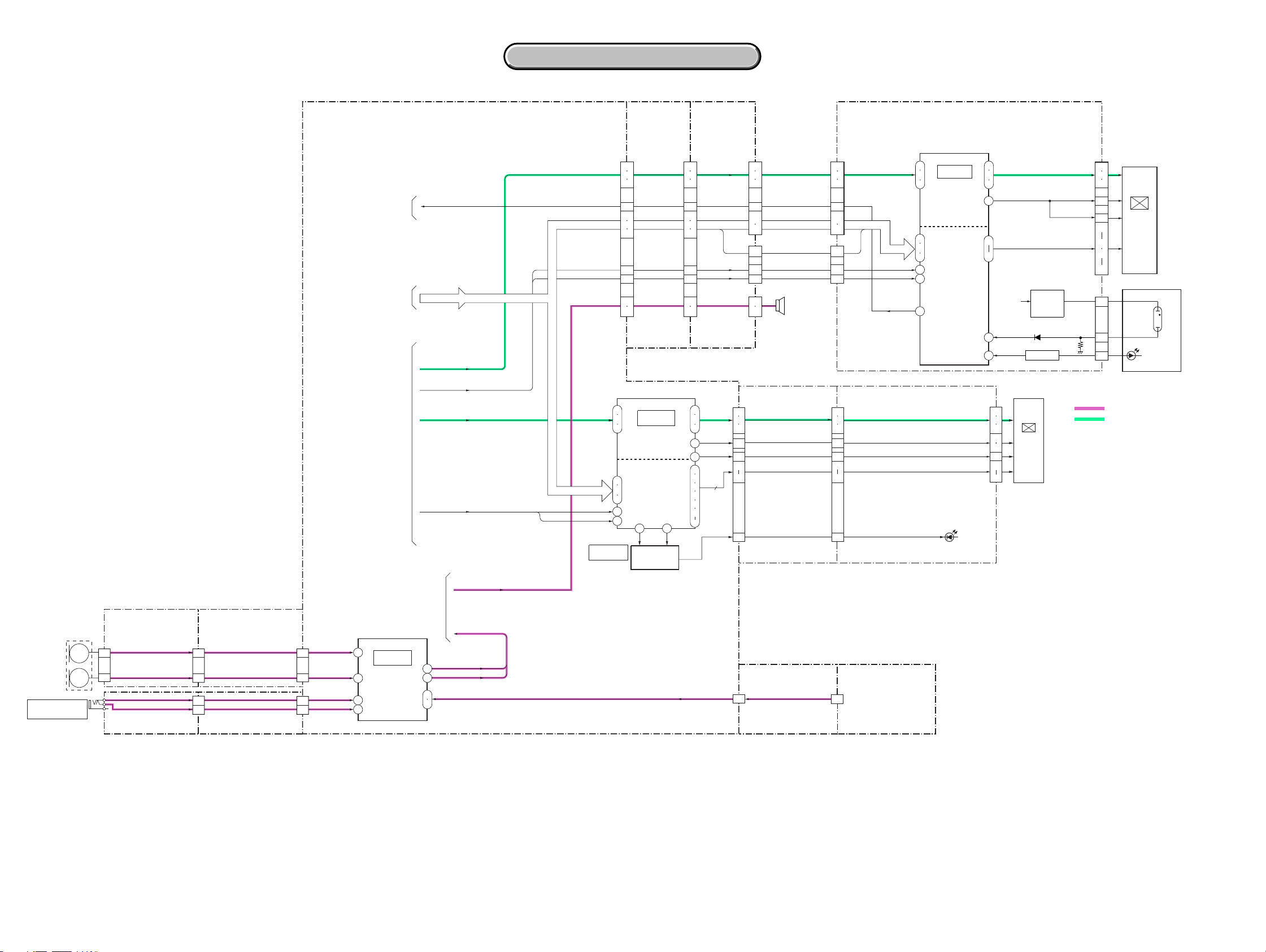
DCR-HC65
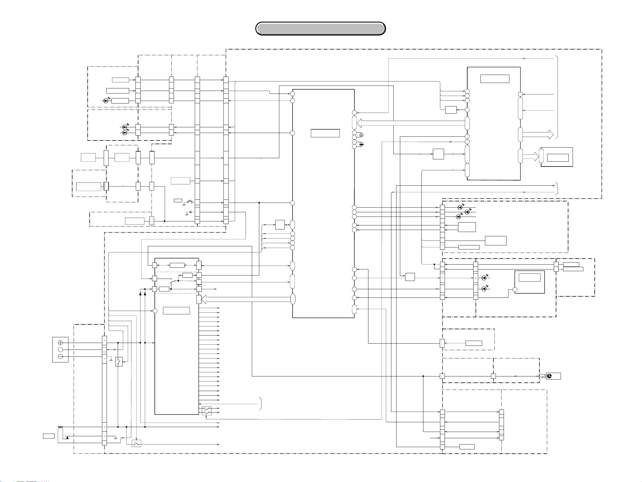
3. BLOCK DIAGRAMS
3. BLOCK DIAGRAMS
3-2. OVERALL BLOCK DIAGRAM (2/4)
MIC901
MIC UNIT
J501
MIC
(PLUG IN POWER)
MI-051 BOARD (2/3)
MIC
MIC
R
CN105 CN1202CN101
1
L
3
JM-016 BOARD (2/2)
16
CN502
26
28
11
10
FP-919
(2/3)
FP-918
(2/3)
(FLEXIBLE)
(FLEXIBLE)
( ) : Number in parenthesis ( ) indicates the division number of schematic diagram where the component is located.
VC-359 BOARD(2/4)
TO
5
OVERALL
BLOCK DIAGRAM (4/4)
(PAGE 3-7)
TO
6
OVERALL
BLOCK DIAGRAM (3/4)
(PAGE 3-5)
TO
3
OVERALL
BLOCK DIAGRAM (1/4)
(PAGE 3-2)
TO
4
OVERALL
BLOCK DIAGRAM (1/4)
(PAGE 3-2)
(17/21)
3
1
11
10
CN1201
35
IC7701
MIC AMP
1
R
3
L
33
BL CONT
VD,SO,SI,SCK
PANEL R
PANEL G
PANEL B
PANEL HD
PANEL VD
EVF R
EVF G
EVF B
EVF HD
EVF VD
22
14
36
SHOE MIC L
48
MIC L
MIC R
SP+
SP-
MIC L
MIC R
EVF R,G,B
EVF HD
EVF VD
IC9302
FP-920
(FLEXIBLE)
(2/3)
CN1203
5
6
7
23
20
22
19
30
31
51
50
34
33
32
45
42
44
48
1
BL ON EXTDA
(15/21)
Q9303
(15/21)
IC9301
RGB
DRIVE
TIMING
GENERATOR
18
BACKLIGHT
DRIVE
CK-141
BOARD
(2/3)
CN151
47
46
45
29
32
30
33
22
21
1
2
20
21
22
26
24
28
17
16
14
12
10
6
31
PANEL R,G B
HD
VD
SP+, SP-
CN9301
10
CN1206
CN152
9
10
8
BL CONT
4
12
VD SI, SCK
14
CN153
CN157
VD SO
1
2
3
1
2
SPEAKER
FP-916 (FLEXIBLE)
15
14
13
17
16
12
3
21
12
SHOE MIC L
CONTROL KEY BLOCK
(FK7800)(1/2)
SP901
PD-219 BOARD(1/2)
CN601
9
10
8
4
12
14
1
2
3
CN602
LB-102 BOARD
7
8
9
5
6
10
EN, VST, REF, PCG, VCK, XSTBY,BLK,HCK1/2, HST
19
1
CN301
INTELLIGENT
2
ACCESSORY
SHOE (1/2)
34
33
32
45
42
44
48
1
31
R,G,B
COM
PSIG
IC602
RGB
DRIVE
TIMING
GENERATOR
D303
BACK
LIGHT
CN302
20
21
22
26
17
5
30
29
VR,VG,VB
COM
BL REG
BL DET
XLED
17
18
16
21
19
20
15
5
Q611
LCD902
COLOR
EVF
UNIT
T600
Q612
INVERTER
BACK
LIGHT
( )
DRIVE
LED DRIVE
COM
COS
CN605
CN606
4
5
3
24
23
22
19
14
2
10
3
2
AUDIO SIGNAL
VIDEO SIGNAL
LCD901
3.5INCH
COLOR
LCD UNIT
ND901
BL HIGH
BL LOW
(STARTER)
BACK
LIGHT
3-3 3-4
Page 17
3. BLOCK DIAGRAMS
3. BLOCK DIAGRAMS
DCR-HC65
3-3. OVERALL BLOCK DIAGRAM (3/4)
CPC
CN1207
FOR ADJUSTMENTS
VC-359 BOARD(3/4)
TO
OVERALL
2
BLOCK DIAGRAM
(1/4)
(PAGE 3-2)
TO
6
OVERALL
BLOCK DIAGRAM
(1/4)
(PAGE 3-3)
6
7
5
TO
7
OVERALL
BLOCK DIAGRAM
(4/4)
(PAGE 3-8)
16
DIGITAL VIDEO/AUDIO SIGNAL
EEP SO, SI, SCK
REC CK
REC DT
RF IN
MC BUS
SPCK
SWP, FRRV, TRRT, TRRV
VSP SO,SI,SCK
VD SO, SCK
VD SO, SI, SCK
HI SO,SI,SCK
REC PROOF
CHIME SDA,CHIME SCK,CHIME VDD
XCC DOWN
SWP
(13/21)
IC8802
EEPROM
562
( ) : Number in parenthesis ( ) indicates the division number of schematic diagram where the component is located.
CPC
CN1207
FOR ADJUSTMENTS
21
VSP SO,SI,SCK
X8801
20MHz
FRRV
TRRT
TRRV
SWP
172
164
(13/21)
IC8801
(2/2)
52
45
33
32
23
178
179
69
70
67
82
83
80
86
87
84
66
65
63
MECHA
CONTROL
|
1
3
CAP FG
190
CAP ON,CAP FWD
165
166
CAP PWM
89
DRUM PWM
88
DRUM FG
197
DRUM PG
198
LOAD,UNLOAD
15
13
TREEL FG
192
SREEL FG
193
TAPE END
31
TAPE TOP
30
DEW AD
119
TAPE LED ON
180
106
MODE SW A - MODE SW C
|
108
41
44
RF MON
(12/21)
IC9101
LPF
LPF
REC CK
REC DT
RF IN
RF MON
RF SWP
SWP
VSP SO, SCK
43
(2/2)
45
CAP ERROR
DRUM ERROR
24
21
(19/21)
IC2301
PWM
DRIVE
75
(1/2)
77
Q2305
SWITCHING
Q2306
SWITCHING
(10/21)
44
IC6501
46
REC/PB
AMP
35
30
39
38
35
38
36
4
80
1
75
CAP VS
77
64
DRUM VS
67
53 52
50
32
33
29
25
21
19
Z MECHA DECK
(MDX-Z200)
CN6501
ODD
EVEN 3
5
6
2
DRUM
10
9
4
3
(12/21)
IC9101
(1/2)
CAPSTAN
FG AMP
CAPSTAN
MOTOR
DRIVE
DRUM
MOTOR
DRIVE
DRUM FG AMP
DRUM PG AMP
LOADING MOTOR
DRIVE MOTOR
REEL FG AMP
TAPE END DETECT
TAPE TOP DETECT
7 8
26 27
22 23
FG 1,2
74
CAP U,V,W
76
78
63
DRUM U,V,W
65
68
49
69
72
20
18
CN9103
CN9101
CN9102
LM +, –
DEW AD
T REEL +, –
S REEL +, –
XCC DOWN
22
25
20
|
17
4
|
1
11
|
14
6
|
1
10
9
1
|
M
4
5
26
25
22
23
20
11
18
12
13
|
15
17
7
|
9
DEW
SENSOR
T REEL
SENSOR
S REEL
SENSOR
TAPE END SENSOR
TAPE TOP SENSOR
D901
TAPE LED
REC PROOF
CONNECTOR
C. C. DOWN
MODE
SWITCH
S902
M903
CAPSTAN
FG
M
M901
M
DRUM FG
DRUM PG
Q901
Q902
4PIN
CAPSTAN
MOTOR
DRUM
MOTOR
M902
LOADING
H902
H901
S903
MIC902
3-5 3-6
Page 18
DCR-HC65
3. BLOCK DIAGRAMS
3. BLOCK DIAGRAMS
3-4. OVERALL BLOCK DIAGRAM (4/4)
FP-923
CN802
CN701
CN602
CN601
PANEL
REVERSE SW
(FLEXIBLE)
2
3
4
FP-921
(FLEXIBLE)
(2/2)
7
9
10
10
.
8
.
9
6
6
.
5
5
4
3
LI 3V
Q2105,Q2106
CK-141 BOARD
.
(3/3)
8
.
9
CN153
.
CN152
CN154
.
LANC SIG
57
45
49
44
BH001
BATTERY
TERMINAL
DC IN
SL-064
BOARD
D801
(EASY)
S801
EASY SW
BATTERY INFO SWS803
Q801
LED DRIVE
MS-210
BOARD (2/2)
D701 (ACCESS)
D702 (CHARGE)
Q601, 602
1
.
TOUCH
PANEL
CONTROL KEY
BLOCK (SB7800)
START/STOP SW
LCD BACKLIGHT SW
S001, 002
TOUCH
2
.
PANEL
4
.
5
CN603
PD-219
BOARD (2/2)
3
.
4
CN604
I/F
2
FP-911
(FLEXIBLE)
VTR DD ON
SHOE ON
BATT/XEXT
FAST CHARGE
11
14
16
17
20
30
27
25
22
21
CN2101
Q2101,
Q2102
BATT SIG
FP-912
(FLEXIBLE)
(3/3)
C
J001
16
( ) : Number in parenthesis ( ) indicates the division number of schematic diagram where the component is located.
VC-359 BOARD(4/4)
FP-920
(FLEXIBLE)
(3/3)
24
40
16
12
51
42
41
43
23
20
18
17
15
.
.
.
56
.
54
51
48
47
14
.
15
KEY AD1
EASY LED
XMS LED ON
XCHARGE LED
TPX
TPY
TP SEL1
KEY AD6
XRESET SW
BATT LI 3V
KEY AD2
LANC OUT
LANC IN
XRESET
VOUT
CAM DD ON
28
12
36
40
10
11
29
32
34
35
37
EVER 3.0V
HI EVER SO,SCK
A 1.2V
D 1.2V
USB 3.1V
MT 5V
A 1.5V
D 1.5V
NS 2.8V
RP 2.8V
A 2.8V
D 2.8V, NS 2.8V
AU 2.8V
EP 2.8V
D 1.9V
CAM 3.1V
A 4.6V
AU 4.6V
EP 4.6V
RP 4.6V
EP 8.5V
13.5V
BL REG
CAM 15V
CAM -7.5V
BATT UNREG
VTR UNREG
SHOE UNREG
1
.
.
9
.
CN1203
BL CONT
3
BATT SIG
5
Q8201
I/F
TO
OVERALL
BLOCK DIAGRAM(2/4)
(PAGE 3-3)
XBATT INFO SW
6
EASY MODE LED ON
17
XCHARGE LED
9
XRESET
73
42
IB SO
.
IB SI
43
VTR DD ON
35
57
SHOE ON
BATT/XEXT
77
FAST CHARGE
37
LANC OUT
40
.
LANC IN
39
14
.
53
VCC
.
62
HI EVER SO
20
.
HI EVER SCK
21
(14/21)
IC8201
HI CONTROL
XCC DOWN
SO
SCK
X 0A
X 1A
X TAL
X TAL
XCAM LED 10
XMEM LED 11
XVTR LED 12
XPOWER SW 1
XMODE SW 2
XEJECT SW 4
SIRCS PWM 45
XF TALLY LED 16
SIRCS SIG 41
SHOE ID2
SHOE ID1
5
23SI
.
24
.
25
52
X8202
32.768KHz
51
29
X8201
10MHz
28
Q1201, 1202
55
.
54
3V REG
5
4
3
CN155
7
9
CN156
S152
PANEL
OPEN/CLOSE SW
S151
RESET
BT151
LITHIUM
BATTERY
(SECONDARY)
LANC I/O
(19/21)
IC2301
DC/DC
CONVERTER
RESET
LANC I/O
CN151
RESET
(2/2)
DRIVE
LED
TXC, RXD, SCK
3
SHOE UNREG
140 KEY AD1
141 KEY AD2
LED
4
3
145 KEY AD6
287 MS LED ON
93 TXD
.
RXD9594
.
SCK
254
IR ON
131
CAM DD ON
137
TP X
.
138
TP Y
.
249
TP SEL1
.
250
TP SEL2
139
KEY AD0
.
142
KEY AD3
.
144
KEY AD5
POWER SW
MODE SW
START/STOP SW
D001 (CAMERA TAPE)
D002 (CAMERA MEMORY)
D003 (PLAY/EDIT)
18
17
5
7
13
.
14
12
CN101
KEY AD3
KEY AD0
KEY AD5
TOUCH
PANEL
CN1208
CN1202
Q8403
I/F
Q8408
DRIVE
7
5
4
9
10
1
2
12
11
24
22
16
.
15
17
FP-919
(FLEXIBLE)
(3/3)
FP-910 (FLEXIBLE)
S001
EJECT SW
CN1205
3
.
4
FP-918 (FLEXIBLE)
(3/3)
26 11
CN1201 CN552
LANC SIG
CONTROL KEY
BLOCK (FK7800)
(2/2)
EXT STROBO
SHOE ID1,2
LANC SIG
SHOE UNREG
RV001
ZOOM VR
CN1206
10
8
.
9
7
6
.
5
3
(6/21)
IC8401
HI CONTROL
(2/2)
REC PROOF
CHIME SDA
CHIME SCK
CHIME AD0
CHIME AD1
CHIME AD2
XHI SCK
EEP TXD
EEP RXD
EEP SCK
HI SO
234
246
.
247
.
134
.
135
.
136
97
.
.
98
HI SI
.
.
99
103
.
104
.
105
CONTROL KEY
BLOCK (PS7800)
PHOTO SW
PHOTO FREEZE
( )
PHOTO REC
D001
(NIGHT SHOT)
D002 (TALLY)
4
IC101
COMMANDER
RECEIVER
MI-051 BOARD (3/3)
JK-268 BOARD
(2/2)
4
INTELLIGENT
6
.
ACCESSORY
5
SHOE
7
(2/2)
8
REMOTE
HI SO,SI,SCK
XCC DOWN
REC PROOF
CHIME SDA
CHIME SCK
CHIME VDD
5
.
2
.
6
ZOOM VR AD
EXT STROBO
CN102
(7/21)
IC8402
EEPROM
4
3
J552
(LANC)
TO
OVERALL
7
BLOCK DIAGRAM(3/4)
(PAGE 3-5)
TO
OVERALL
1
BLOCK DIAGRAM(1/4)
(PAGE 3-1)
S001
FOCUS SW
BACK LIGHT SW
S002
FP-909
(FLEXIBLE)
3-7 3-8
Page 19
3. BLOCK DIAGRAMS
3. BLOCK DIAGRAMS
DCR-HC65
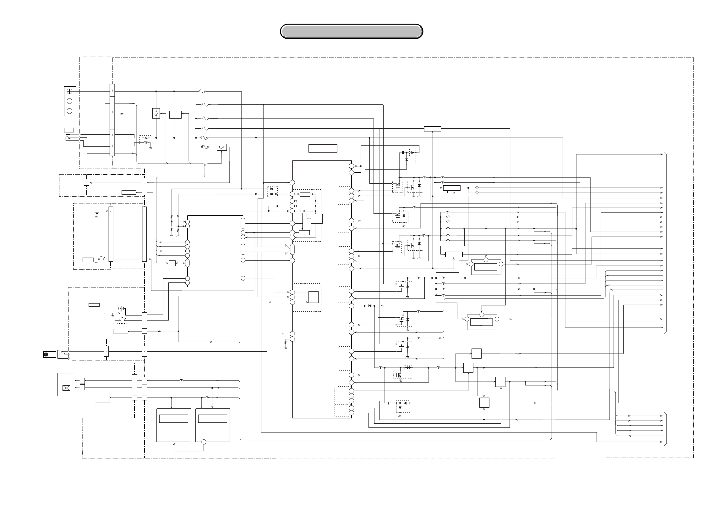
3-5. POWER BLOCK DIAGRAM (1/2)
(LANC)
FP-912
(FLEXIBLE)
BH001
BATTERY
TERMINAL
C
J001
DC IN
INTELLIGENT
ACCESSORY
SHOE
8
CONTROL KEY
BLOCK (FK7800)
LI 3V
BT151
LITHIUM
BATTERY
(SECONDARY)
CK-141
BOARD
(1/2)
S151
RESET
CN151
POWER
CONTROL
KEY
BLOCK
(PS7800)
LCD902
COLOR
EVF
UNIT
BOARD
LB-102 BOARD
CN302
2
8
16
CN552
D303
BACK
LIGHT
LED
FP-916
(FLEXIBLE)
J552
VC-359 BOARD (1/2)
CN2101
11
BATT UNREG
14
BATT SIG
16
17
20
30
ACV UNREG
27
25
22
BATT/XEXT
21
RV001
18
17
FP-920
(FLEXIBLE)
(1/2)
XRESET
OFF (CHG)
ON
MODE
MODE LED
D001-003
FP-918JK-268
(FLEXIBLE)
9
8
CN301
CN1203
XPOWER SW
XMODE SW
23
•
22
3
2
LF2101
35
34
3220
9
10
6
23
24
1
19
20
6
5
4ZOOM VR
•
Q2101,
2102
FAST CHARGE
CN1206
SHOE UNREG
BATT SIG
CN1208
R1218
CN1201
CN9301
IC9302 IC9301
BACK LIGHT
( ) : Number in parenthesis ( ) indicates the division number of schematic diagram where the component is located.
F007
F001
F004
F002
F003
F006
18
2.8V/4.6V UNREG
BL UNREG
C/D/MT UNREG
VTR UNREG
SHOE ON
(14/21)
IC8201
HI CONTROL
L9302
RGB
DRIVE
TIMING
GENERATOR
Q2103,
2104
CHARGE
SWITCH
INIT CHARGE ON
BATT SENS
65
ACV SENS
66
SHOE ON
57
BATT/XEXT
77
INIT CHARGE ON
38
FAST CHARGE
37
Q8201
I/F
L9303
42
43
1
2
IB SO
IB SI
XPOWER SW
XMODE SW
(15/21) (15/21)
DRIVE
BL ON
Q2105,2106
BATT UNREG
XRESET
BATT IN
HI EVER SO
HI EVER SCK
XCS DD
VTR DD ON
XLANC PWR ON
D 2.8V
EP 8.5V
EP 2.8V
EP 4.6V
Q2317-2319
5V REG
MT 5V
(19/21)
IC2301
DC/DC CONVERTER
RESET,LANC I/O
63
VCC01
67
VCC02
61
D2301
D2302
14
VCC
53
62
73
31
20
21
67
35
7
VOUT
VCC1
64
49
3V REG
47
46
45
48
51
50
14
15
13
44
55
60
58
43
38
DIN
CLK
LD
CTL1
VCC3
VOUT4
VREF
RT
RESET
LANC I/O
BATTERY
IN
DETECT
5.6V
REG
OUT1-1
OUT1-2
+INE2
OUT3-1
OUT3-2
+INE5
+INE6
VCONT6
VOUT6
REG6CTL
VCONT5
VOUT5
OUT2
OUT4
OUT5
OUT6
OUT7
66
12
IN1
68
29
70
72
10
IN3
41
VR
73
9
IN4
62
VB
IN7
Q2303
75
24
77
21
79
6
3
4
5
1
2
L2301
Q2301
SWITCHING
Q2303
SWITCHING
Q2302
SWITCHING
Q2304
SWITCHING
4.6 V
Q2305
SWITCHING
Q2306
SWITCHING
L2307
L2305
L2302
L2303
Q2307
SWITCHING
D2304
RECT
D2305
RECT
L2308
Q2309
L2306
Q2308
CAP VS
CAP ERROR
DRUM VS
DRUM ERROR
L2304
L2310
L2309
L2319
L2320
L2321
L2322
Q2313,Q2314
1.2V REG
L2313
L2314
L2315
L2316
L2317
L2318
Q2320,Q2321
1.9V REG
Q2310
15V
REG
D 1.5V
A 1.5V
L2325
L2326
IC2302
3.1V REG
1
IC2303
3.1V REG
Q2312
13.5V
REG
-7.5V
REG
A 1.2V
D 1.2V
1
(19/21)
Q2315,
2316
(19/21)
45
Q2311
BL CONT
BL REG
AL 2.8V
PR 2.8V
A 2.8V
D 2.8V
AU 2.8V
EP 2.8V
D 1.9V
45
8.5V
REG
USB 3.1V
A 4.6V
AU 4.6V
EP 4.6V
RP 4.6V
CAM 3.1V
13.5V
CAM 15V
EP 8.5V
CAM -7.5V
CAM DD ON
NS 2.8V
A 1.2V
D 1.2V
VTR UNREG
AU 4.6V
AU 2.8V
RP 4.6V
RP 2.8V
A 2.8V
A 1.5V
D 1.5V
USB 3.1V
D 1.9V
D 2.8V
MT 5V
A 4.6V
CAP VS
CAP ERROR
DRUM VS
DRUM ERROR
CAM DD ON
CAM 15V
CAM -7.5V
13.5V
CAM 3.1V
AL 2.8V
EP 4.6V
EP 8.5V
EP 2.8V
BL REG
BL CONT
EVER 3.0V
1
TO
POWER
BLOCK
DIAGRAM
(2/2)
(PAGE 3-11)
2
TO
POWER
BLOCK
DIAGRAM
(2/2)
(PAGE 3-12)
3-9 3-10
Page 20
DCR-HC65
3. BLOCK DIAGRAMS
3. BLOCK DIAGRAMS
3-6. POWER BLOCK DIAGRAM (2/2)
VC-359 BOARD(2/2)
NS 2.8V
A 1.2V
D 1.2V
VTR UNREG
AU 4.6V
AU 2.8V
RP 4.6V
TO
POWER BLOCK
1
DIAGRAM
(1/2)
(PAGE 3-10)
16
RP 2.8V
A 2.8V
A 1.5V
D 1.5V
USB 3.1V
D 1.9V
D 2.8V
MT 5V
A 4.6V
CAP VS
CAP ERROR
DRUM VS
DRUM ERROR
CAM DO ON
CAM 15V
CAM -7.5V
13.5V
CAM 3.1V
AL 2.8V
( ) : Number in parenthesis ( ) indicates the division number of schematic diagram where the component is located.
IC6401
DV SIGNAL
PROCESS
RF SIGNAL
PROCESS
MI-051 BOARD
CN101
15
•
16
2
4
9
•
10
20
CN103
5
IC7701
MIC
AMP
DIGITAL STILL PROCESS
AUDIO SIGNAL PROCESS
VIDEO
IN/OUT
AGC
ACC
AL 2.8V
D102
TALLY LED
D101
NIGHT SHOT LED
FS-087 BOARD
2
CN851
IC6201
DV SIGNAL PROCESS
MPEG MOVE PROCESS
FB6201
MANUAL FOCUS
PHOTO SENSOR
L5103
IC101
COMMANDER
PH0851, 0852
IC6202
REMOTE
RECEIVER
(13/21)
IC8802
EEPROM
64Mbit
SDRAM
(2/21)(11/21)(9/21)
IC5101IC7101
FOCUS/ZOOM/
IRIS/ND
DRIVE
A1.2V
A 4.6V
(13/21)
IC8801
CAMERA
CONTROL
MECHA
CONTROL
IC5201
CAMERA
PROCESS
153
55
2
XREEL
HALL ON
ZM RST LED
IC1201
(1/21)
IC5003
AGC
A/D CONV.
TO
POWER
BLOCK DIAGRAM
(1/2)
(PAGE 3-10)
4
(21/21)
2.9V
REG
5
D 2.8V
MS VCC
A 4.6V
R1244
EVER 3.0V
1
FP-919
(FLEXIBLE)
CN1202
NS 2.8V
R1202
A 4.6
R1219,
R1220
R1205
14
•
13
27
25
20
•
19
9
D 2.8V
FP-922
(FLEXIBLE)
Q7605
VTR UNREG SP VCC
REGREG
AU 4.6V
AU 2.8V
D 2.8V
D 1.9V
CAM DO ON
RP 4.6V
RP 2.8V
A 2.8V
A 1.5V
D 1.5V
USB 3.1V
A 1.2V
D 1.2V
D 2.8V
VTR UNREG
MT 5V
A 2.8V A 2.8V
D 2.8V
A 4.6V
D 1.9V
(16/21) (17/21)
IC7601
AUDIO
I/O
D/A CONV.
A/D CONV.
(10/21) (8/21) (4/21) (5/21) (3/21)
IC6501
REC/PB
AMP
IC6301
DV
INTERFACE
EP 8.5V
EP 4.6V
EP 2.8V
BL CONT
BL REG
R1245
CN1203
33
13
14
15
16
17
18
23
26
27
38
39
46
47
CHIME PWR CONT
A 2.8V
FP-920
(FLEXIBLE)
(2/2)
•
•
•
•
•
2
•
CAM DD ON
MS VCC ON
CN151
19
CK-141
BOARD
(2/2)
38
•
39
36
•
37
34
•
35
29
25
•
26
13
•
14
50
6
•
5
(6/21) (7/21) (7/21)
FB8402
IC8402
EEPROM
DRUM ERROR
D 2.8V
VTR UNREG
MT 5V
3.4V
CAP ERROR
IC8401
131
HI
286
CONTROL
DIGITAL
130
STILL
CONTROL
USB 3.1V
D1.2VD1.2V
D2.8V
5 4
(1/21)
IC5002
3.4V REG
ZM RST LED
CN155
CN153
CN152
CN156
13.5V
CAP VS
DRUM VS
CAM 15V
CAM -7.5V
CAM 3.1V
Q5101
FP-923
(FLEXIBLE)
2
6
5
4
4
3
8
10
2
FP-921
(FLEXIBLE)
(7/21)
IC8403
IC8403
XTAL
XTAL
OSC
OSC
(12/21)
IC9101
CAPSTAN MOTOR DRIVE
75
CAPSTAN FG AMP
77
MOTOR DRIVE
DRUM FG,PG AMP
45
MOTOR DRIVE
43
REEL FG AMP
TAPE TOP,END DET
64
DRUM,CAP ERROR AMP
67
(1/21)
IC5001
60
TIMING
GENERATOR
ZM VCC
MR A2.8V
DRUM
LOADING
SL-064 BOARD
EASY LED
5
CN802
PD-219 BOARD
CN602
6
5
4
CN601
4
3
ACCESS LED
8
10
2
CN701
MS-210
BOARD
(7/21)
IC8404
NAND
GATE
FB8501
Q8404-8406
R9120
FP-913 (FLEXIBLE)
CD-513 BOARD
CN201
27
7
6 28
93225
2
CN5001
CN5101
29
3
D801
31
D701
D702
CHARGE
Q9101
CHIME PWR CONT
XREEL HALL ON
ZOOM
RESET
SENSOR
FOCUS
MR
SENSOR
IC602
RGB
DRIVE
TIMING
GENERATOR
INVERTER
(BACKLIGHT DRIVE)
Q612, T600
9
SENSOR VCC
IC201
CCD
IMAGER
LENS ASSY
IC8502
IC8503
CHIME VDD
TAPE LED A
10
CN702
MEMORY
STICK
Duo
CONNECTOR
(7/21)
16M
SDRAM
(7/21)
32M
FLASH
MEMORY
CN9102
L401
Q608, 609
CN605
CN606
BL HIGH
13
27
19
Z MECHA DECK
(MDX-Z200)
IC202
S/H
IC401
18
10
4PIN
CONNECTOR
T REEL,
S REEL
SENSOR
TAPE LED
PITCH/YAW
SENSOR
AMP
LCD901
3.5INCH
COLOR
LCD
UNIT
ND901
BACK
LIGHT
MIC902
H901,
H902
D901
SE401, 402
PITCH/YAW
SENSOR
3-11 3-12E
Page 21
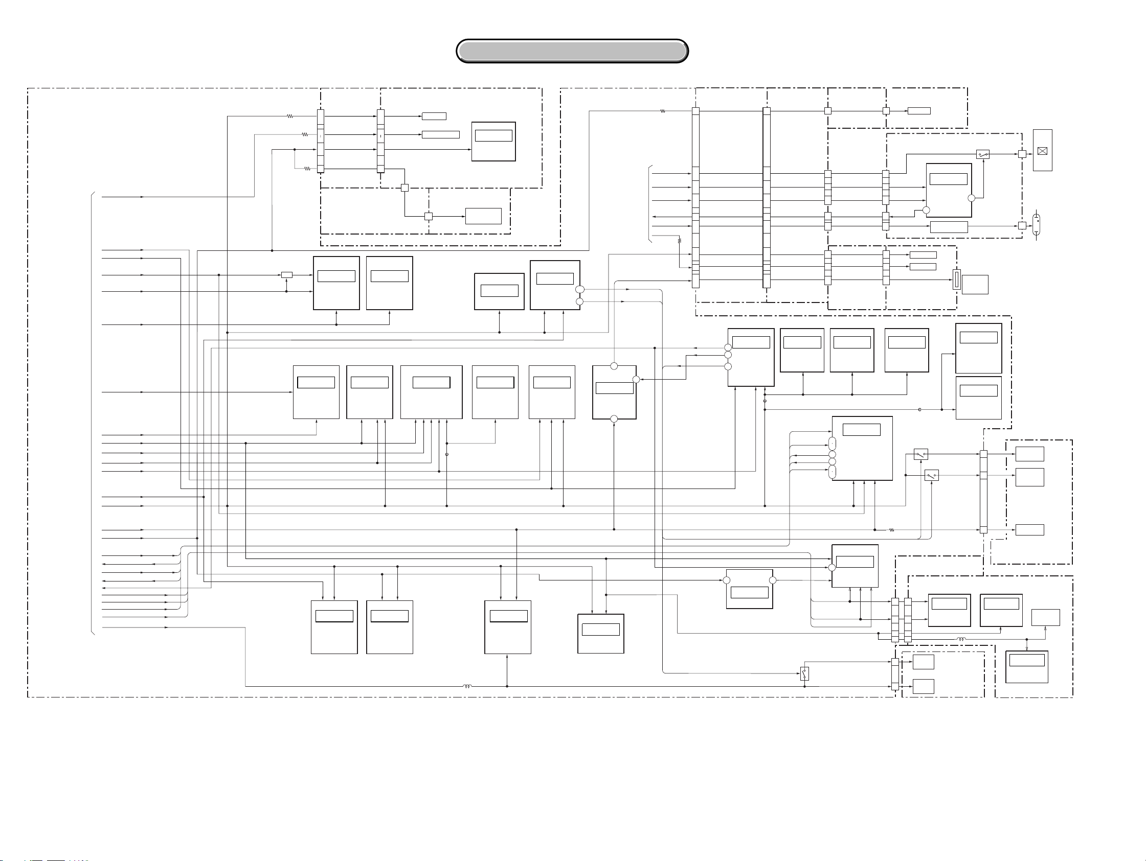
SECTION 4
PRINTED WIRING BOARDS AND SCHEMATIC DIAGRAMS
4-1. FRAME SCHEMATIC DIAGRAM (1/2)
3
LENS UNIT
123456789
F_MR_B
F_MR_A
ZOOM_A
ZOOM_XA
F_MR_VCC
MR_TEMP_GND
LENS_TEMP_OUT
MI-051
BOARD
CN105
4P
1
INT_MIC_L
2
GND
3
INT_MIC_R
GND
4
6PCN103
1
REG_GND
2
MF_A
3
REG_GND
4
MF_B
5
MF_LED_A
FP-922
6
MF_LED_K
6P
CN102
1
REG_GND
2
REG_GND
BACK LIGHT
3
FOCUS
4
REG_GND
5
REG_GND
6
10PCN5010
1
AUDIO L
2
N.C.
3
S GND
4
N.C.
S-C
5
AUDIO R
6
JACK AD
7
VIDEO/AUDIO GND
8
VIDEO IN/OUT
9
S-Y
10
JM-016
BOARD
JK-268
BOARD
10111213141516171819202122232425262728
FOCUS-
FOCUS+
ZOOM_B
N_DRIVE-
N_DRIVE+
ND_BIAS-
CN101
CN502
ND_BIAS+
ND_HALL-
28P
BACK Light SW
XF_TALLY_LED
XF_TALLY_LED
12P
VIDEO/AUDIO GND
12PCN552
LANC_JACK_IN
ZOOM_XB
A
B
C
D
E
F
G
H
I
J
K
L
1
FS-087 BOARD
CN0851
FP-909
FLEXIBLE
16
6P
REG_GND
REG_GND
MF_LED_A
MF_LED_K
MIC
(PLUGIN POWER)
MIC901
MIC UNIT
L-CH
R-CH
MF_A
MF_B
AV IN/OUT
J501
(HEADPHONE)
CN501
J552
J551
(LANC)
29P
CN5101
6
5
4
3
2
1
ND_HALL+
IR_SW_OUT
INT_MIC_R
MIC_GND
INT_MIC_L
MIC_GND
MIC_GND
MF_LED_K
MF_LED_K
MF_LED_A
FOCUS SW
SIRCS_SIG
REG_GND
A_4.6V
A_4.6V
REG_GND
NS_LED_K
NS_LED_K
NS_LED_K
NS_LED_A
NS_LED_A
NS_LED_A
MIC_GND
EXT_MIC_R
EXT_MIC_L
REG_GND
AUDIO L
AUDIO R
VIDEO IN/OUT
JACK AD
REG_GND
LANC_SIG
LANC_DC
REG_GND
REG_GND
HP_JACK_IN
HP_GND
HP_GND
IR_SW_GND
MF_B
MF_A
TALLY
TALLY
N.C.
S GND
S-C
S-Y
HP_R
HP_L
I_BIAS+
5
I_HALL+
28
27
26
25
24
23
22
21
20
19
18
17
16
15
14
13
12
11
10
9
8
7
6
5
4
3
2
1
12
11
10
9
8
7
6
5
4
3
2
1
12
11
10
9
8
7
6
5
4
3
2
1
I_BIAS-
I_HALL-
I_DRIVE-
I_DRIVE+
FP-919 FLEXIBLE
FP-918 FLEXIBLE
4-2. SCHEMATIC DIAGRAMS 4-3. PRINTED WIRING BOARDS
4-2. SCHEMATIC DIAGRAMS 4-3. PRINTED WIRING BOARDS
684 17 182
7
91411 12 16
CD-513 BOARD
CCD
IMAGER
33P
H2
LH
1011121314151617181920212223242526272829303132
XSHD
H1
RG
GND
CCD_OUT+
CLPDM
GND
XSHP
GND
CCD_OUT-
GND
A_2.8V
GND
GND
RCSUB
CAM_15V
GND
CAM_-7.5V
FP-913 FLEXIBLE
H2
H1
LH
GND
GND
GND
GND
XSHP
XSHD
CCD_OUT-
GND
CCD_OUT+
1011121314151617181920212223242526272829303132
GND
GND
CLPDM
A_2.8V
RCSUB
CAM_15V
GND
CAM_-7.5V
V4
V3
V2
V1
33
123456789
V1
V4
V3
V2
(FOR CHECK)
1234567
SWP
RF_MON
8P
CN1207
ZM_OUT
10
11
12
13
14
15
16
17
18
19
20
21
22
23
24
25
26
27
ZM_GND
1
2
3
4
5
6
7
8
9
29
ZM_VCC
MAKER_SELECT
INT_MIC_R
MIC_GND
INT_MIC_L
MIC_GND
MIC_GND
MF_LED_K
MF_LED_K
MF_B
MF_LED_A
MF_A
FOCUS SW
BACK Light SW
TALLY
TALLY
XF_TALLY_LED
XF_TALLY_LED
SIRCS_SIG
REG_GND
A_4.6V
A_4.6V
REG_GND
NS_LED_K
NS_LED_K
NS_LED_K
NS_LED_A
NS_LED_A
NS_LED_A
A_2.8V
A_2.8V
YAW_AD
VST_C_RESET
YAW_AD
VST_C_RESET
REG_GND
REG_GND
PITCH_AD
PITCH_AD
REG_GND
REG_GND
VSUBRGGND
VSUB
REG_GND
CN201
123456789
33
REG_GND
33P
CN5001
27PCN1202
VC-359 BOARD(1/2)
27PCN1201
JACK AD
1
REG_GND
2
3
VIDEO IN/OUT
4
S-Y
5
S-C
REG_GND
6
AUDIO R
7
AUDIO L
8
REG_GND
9
EXT_MIC_L
10
EXT_MIC_R
11
EXT_MIC_GND
12
REG_GND
13
REG_GND
14
REG_GND
15
REG_GND
16
HP_L
17
REG_GND
18
HP_R
19
HP_JACK_INLANC_DC
20
REG_GND
21
REG_GND
22
LANC_DC
23
LANC_DC
24
LANC_JACK_IN
25
LANC_SIG
26
REG_GND
27
DCR-HC65
D_2.8V
EVF_EN
EVF_VB
EVF_VG
EVF_VR
EP_2.8V
EP_4.6V
LED_K
1510
1
2
3
4
5
6
7
8
9
10
1
2
3
4
5
6
7
8
9
10
11
12
13
14
1
2
3
4
5
6
23
22
1
21
2
20
3
19
4
18
5
17
6
16
7
15
8
14
9
13
10
12
11
11
12
10
13
9
14
8
15
FP-916 FLEXIBLE
7
16
6
17
5
18
4
19
3
20
2
21
1
CONTROL KEY
BLOCK
(PS7800)
CONTROL KEY
BLOCK
(FK7800)
INTELLIGENT
ACCESSORY
SHOE
FP-910
FLEXIBLE
23P
CN301
EVF_VDD
EVF_VDD
EVF_GND
EVF_GND
HST
HCK1
HCK2
BLK
STB
VCK
PCG
REF
VST
EN
VB
VG
VR
PSIG
COM
EVF_GND
EP_2.8V
EP_4.6V
LED_K
LB-102 BOARD
21PCN302
1
N.C.
VDD
2
3
VSS
4
VSSG
HST
GREEN
5
HCK2
6
HCK1
7
SCAN
8
WIDE
9
REF
10
XSTB
11
VST
12
VCK
13
ENB
14
PCG
15
BLUE
16
RED
17
18
CS
19
PSIG
20
COM
21
LCD902
COLOR EVF
UNIT
13
TO
VC-359 BOARD(2/2)
CPC
8
XCS_EEP
EEP_SCK
EEP_SO
EEP_SI
GND
CN1208
10P
KEY_AD3
KEY_AD0
REG_GND
XVTR_LED
XMEM_LED
MODE_LED_VDD
XCAM_LED
REG_GND
XPOWER_SW
XMODE_SW
CN1206
14P
REG_GND
REG_GND
ZOOM_VR_AD
SHOE_UNREG
SHOE_UNREG
LANC_SIG
HOTSHOE_ID1
HOTSHOE_ID2
EXT_STROBO
SHOE_MIC_GND
SHOE_MIC_L
SHOE_UNREG_GND
SHOE_UNREG_GND
CN1205
6P
REG_GND
REG_GND
XEJECT_SW
XEJECT_SW
REG_GND
REG_GND
21PCN9301
EVF_VDD
EVF_GND
EVF_HST
EVF_HCK1
EVF_HCK2
EVF_BLK
EVF_STB
EVF_VCK
EVF_PCG
EVF_REF
EVF_VST
EVF_PSIG
EVF_COM_CS
EVF_GND
GND
4-1 4-2
FRAME SCHEMATIC DIAGRAM (1/2)
Page 22

DCR-HC65
FRAME SCHEMATIC DIAGRAM (2/2)
4-2. SCHEMATIC DIAGRAMS 4-3. PRINTED WIRING BOARDS
4-2. SCHEMATIC DIAGRAMS 4-3. PRINTED WIRING BOARDS
TO
CAPSTAN
MOTOR
TO
LOADING MOTOR,
SK SENSOR,
MODE SW ETC
TO
DRUM
MOTOR
TO
VIDEO HEAD
2
CN9103
CAP_V
CAP_V
CAP_V
CAP_V
HE_GND
UHE+
UHE-
VHE+
VHE-
WHE+
CAP_W
CAP_W
CAP_W
CAP_W
WHE-
HE_VCC
CAP_U
CAP_U
CAP_U
CAP_U
N.C.
FG1
FG_VCC
FG2
FG_GND
FG_GND
CN9102
LM_LOAD
LM_LOAD
LM_UNLOAD
LM_UNLOAD
DEW+
DEW-
XMODE_SW_A
XMODE_SW_B
XMODE_SW_C
SW_COM/SW_GND
TAPE_TOP
XREC_PROOF
CHIME_VDD
CHIME_SDA
CHIME_SCK
MIC/REC_SW_GND
XCCDOWN_SW
TAPE_LED_K
TAPE_LED_A
TAPE_END
SREEL+
SREEL-
HALL_GND
TREEL-
TREEL+
HALL_VCC
CN9101
FG
PG
FG/PG_COM
M_COM
DRUM_U
DRUM_U
DRUM_W
DRUM_W
DRUM_V
DRUM_V
CN6501
GND
YSDL
XSDL
GND
XODD
YODD
GND
YEVEN
XEVEN
GND
27P
27P
10P
10P
1
2
3
4
5
6
7
8
9
10
11
12
13
14
15
16
17
18
19
20
21
22
23
24
25
26
27
1
2
3
4
5
6
7
8
9
10
11
12
13
14
15
16
17
18
19
20
21
22
23
24
25
26
27
10
9
8
7
6
5
4
3
2
1
10
9
8
7
6
5
4
3
2
1
1
A
Z-MECHA
DECK
(MDX-Z200)
B
C
D
E
F
G
H
I
J
4
VC-359 BOARD
(2/2)
K
TO
VC-359 BOARD
(1/2)
5
CN1203
51P
REG_GND
REG_GND
PANEL_R
PANEL_G
PANEL_B
REG_GND
TP_SEL1
PANEL_8.5V
PANEL_8.5V
PANEL_4.6V
PANEL_4.6V
PANEL_2.8V
PANEL_2.8V
VD_SCK
XCS_LCD
BL_CONT
BL_GND
BL_GND
BL_REG
BL_REG
KEY_AD1
KEY_AD6
PANEL_HD
PANEL_VD
XRESET_SW
BATT_LI_3V
BATT_LI_3V
KEY_AD2
ACCESS_LED
REG_GND
MS_DIO
MS_INSERT
MS_SCLK
MS_VCC
MS_VCC
REG_GND
REG_GND
REG_GND
REG_GND
REG_GND
USB_D-
USB_DET
USB_D+
BATT_SIG
BATT_GND
BATT_GND
BATT_GND
BATT_GND
BATT/XEXT
ACV_GND
ACV_GND
ACV_GND
ACV_GND
ACV_UNREG
ACV_UNREG
ACV_UNREG
ACV_UNREG
VD_SO
VD_SI
D_2.8V
D_2.8V
MS_BS
TP_X
TP_Y
TPB+
TPA+
1
2
3
4
5
6
7
8
9
10
11
12
13
14
15
16
17
18
19
20
21
22
23
24
25
26
27
28
29
30
31
32
33
34
35
36
37
38
39
40
41
42
43
44
45
46
47
48
49
50
SP-
51
SP+
1
2
TPB-
3
4
5
TPA-
6
7
8
9
10
11
12
FP-912
13
FLEXIBLE
14
15
N.C.
16
17
18
19
20
21
22
23
24
25
26
N.C.
27
28
29
30
CN2101
STROBO_LED_ON
CHARGE LED A
XBATT_INFO_SW
EASY MODE LED A
XEASY_MODE_LED
30P
BATT_UNREG
BATT_UNREG
BATT_UNREG
BATT_UNREG
7610
CN151
51P
STROBO_LED_ON
51
CHARGE LED A
50
REG_GND
49
REG_GND
48
47
PANEL_R
PANEL_G
46
PANEL_B
45
REG_GND
44
TP_SEL1
43
TP_X
42
TP_Y
41
XBATT_INFO_SW
40
39
PANEL_8.5V
PANEL_8.5V
38
PANEL_4.6V
37
PANEL_4.6V
36
35
PANEL_2.8V
PANEL_2.8V
34
33
VD_SCK
32
VD_SO
XCS_LCD
31
VD_SI
30
BL_CONT
29
28
BL_GND
27
BL_GND
26
BL_REG
BL_REG
25
24
KEY_AD1
23
KEY_AD6
22
PANEL_HD
21
PANEL_VD
FP-920 FLEXIBLE
20
XRESET_SW
19
EASY MODE LED A
18
BATT_LI_3V
17
BATT_LI_3V
16
XEASY_MODE_LED
15
KEY_AD2
14
D_2.8V
13
D_2.8V
12
ACCESS_LED
11
REG_GND
10
MS_BS
9
MS_DIO
8
MS_INSERT
7
MS_SCLK
6
MS_VCC
5
MS_VCC
4
REG_GND
3
REG_GNDTOP/END_GND
2
SP-
1
SP+
81114
CK-141 BOARD
CN001
(USB)
CN002
(I link)
BH001
BATTERY
TERMINAL
J001
DC IN
912
10PCN602
1
VD_SO
2
PANEL_XHD
3
PANEL_XVD
4
EP_2.8
5
EP_4.6
6
EP_8.5
7
REG_GND
8
TP_Y
9
TP_SEL1
10
TP_X
14PCN601
1
SE_GND
2
BL_GND
3
BL_REG
4
BL_CNT
5
BL_ON
6
2ND_S/S
7
REG_GND
8
PANEL_B
9
PANEL_R
10
PANEL_GFG_VCC
11
REG_GND
12
VD_SI
13
XCS_LCD
14
VD_SCK
FP-911
FLEXIBLE
6P
CN802
1
REG_GND
2
KEY_AD1
3
BATT_INFO
4
EASY LED
5
EASY MODE LED A
6
REG_GND
SL-064 BOARD
1
REG_GND
2
MS_VCC
3
MS_SCLK
MS_INSERT
4
MS_DIO
5
MS_BS
6
ACCESS_LED
7
8
D_2.8V
9
CHARGE LED
CHARGE LED A
10
SP901
SPEAKER
PD-219 BOARD
10PCN701
10
9
8
7
6
5
4
3
2
1
CN702
GND
VCC
SCLK
N.C.
INS
N.C.
DIO
N.C.
BS
GND
10P
BT151
LITHIUM BATTERY
(SCONDARY)
CN152
10PCN153
14P
CN155
EASY MODE LED A
CN156
VD_SO
PANEL_XHD
PANEL_XVD
EP_2.8
EP_4.6
EP_8.5
REG_GND
TP_SEL1
SE_GND
BL_GND
BL_REG
BL_CNT
BL_ON
2ND_S/S
REG_GND
PANEL_B
PANEL_R
PANEL_G
REG_GND
XCS_LCD
VD_SCK
6PCN154
REG_GND
REG_GND
PANEL_RVS
PANEL_RVS
REG_GND
REG_GND
CN157
REG_GND
KEY_AD1
BATT_INFO
EASY LED
REG_GND
10P
REG_GND
MS_VCC
MS_SCLK
MS_INSERT
MS_DIO
MS_BS
ACCESS_LED
D_2.8V
CHARGE LED
CHARGE LED A
VD_SI
TP_Y
TP_X
SP+
6P
2P
SP-
1
2
3
4
5
6
7
8
9
10
1
2
3
4
5
6
7
8
9
10
11
12
13
14
6
5
4
3
2
1
1
2
6
5
4
3
2
1
FP-923
FLEXIBLE
1
2
3
4
5
6
7
8
9
10
PC-131
HARNESS
PC-132
HARNESS
FP-921
FLEXIBLE
MS-210 BOARD
CN605
CN606
CN603
CN604
MEMORY STICK Duo
CONNECTOR
24P
10P
6P
TP_BOT
TP_TOP
6P
REG_GND
2ND_S/S_SW
BL_ON/OFF_SW
REG_GND
VSSG
XSTBY
TEST1
WIDE
HCK2
HCK1
TEST2
15
COM
DWN
PSIG
TP_R
TP_L
24
23
COS
VST
22
21
VCK
20
EN
19
18
VDD
VSS
17
16
N.C.
15
14
13
PCG
12
HST
11
REF
10
9
8
7
6
5
G
4
R
3
B
2
RGT
1
1LED_GND
2LED
3BL_LOW
4N.C
5N.C
6N.C
7N.C
8N.C
9N.C
10BL_HIGH
1
2
3
N.C.
4
5
N.C.
6
1
2
N.C.
3
4
5
N.C.
6
16
LCD901
3.5INCH
COLOR
LCD UNIT
CONTROL KEY
BLOCK(SB7800)
17133
ND901 BACK LIGHT
TOUCH PANEL
L
FRAME SCHEMATIC DIAGRAM (2/2)
4-3 4-4
Page 23

Link
Link
DCR-HC65
4-2. SCHEMATIC DIAGRAMS
CD-513 BOARD
CD-513 BOARD
CK-141 BOARD
CK-141 BOARD
FP-911 FLEXIBLE BOARD FP-909 FLEXIBLE BOARD
FP-911 FLEXIBLE BOARD FP-909 FLEXIBLE BOARD
JK-268 BOARD
JK-268 BOARD
JM-016 BOARD
JM-016 BOARD
PD-219 BOARD
PD-219 BOARD
CONTROL KEY BLOCK
CONTROL KEY BLOCK
LB-102 BOARD
LB-102 BOARD
MS-210 BOARD
MS-210 BOARD
(CCD IMAGER)
(CCD IMAGER)
(RELAY, FUNCTION KEY)
(RELAY, FUNCTION KEY)
(JACK)
(JACK)
(JACK-2)
(JACK-2)
(RGB DRIVE, TIMING GENERATOR)
(RGB DRIVE, TIMING GENERATOR)
(SB7800)
(SB7800)
(EVF BACK LIGHT)
(EVF BACK LIGHT)
(MS CONNECTOR)
(MS CONNECTOR)
MI-051 BOARD
MI-051 BOARD
FS-087 BOARD
FS-087 BOARD
SL-064 BOARD
SL-064 BOARD
FP-910 FLEXIBLE BOARD
FP-910 FLEXIBLE BOARD
FP-912 FLEXIBLE BOARD
FP-912 FLEXIBLE BOARD
CONTROL KEY BLOCK
CONTROL KEY BLOCK
CONTROL KEY BLOCK
CONTROL KEY BLOCK
FP-228/FP-467/FP-826 FLEXIBLE BOARD
FP-228/FP-467/FP-826 FLEXIBLE BOARD
(INDICATOR, IR SENSOR)
(INDICATOR, IR SENSOR)
(MF PHOTO SENSOR)
(MF PHOTO SENSOR)
(FUNCTION KEY)
(FUNCTION KEY)
(PS7800)
(PS7800)
(FK7800)
(FK7800)
COMMON NOTE FOR SCHEMATIC DIAGRAMS
COMMON NOTE FOR SCHEMATIC DIAGRAMS
Page 24

4-2. SCHEMATIC DIAGRAMS
Front of the lens
Pattern box
1.0 m (PTB-450)
0.4m (PTB-1450)
4-2. SCHEMATIC DIAGRAMS
THIS NOTE IS COMMON FOR SCHEMATIC DIAGRAMS
(In addition to this, the necessary note is printed in each block)
(For schematic diagrams)
• All capacitors are in µF unless otherwise noted. pF : µ
Link
µF. 50 V or less are not indicated e xcept for electrolytics
and tantalums.
• Chip resistors are 1/10 W unless otherwise noted.
kΩ=1000 Ω, MΩ=1000 kΩ.
• Caution when replacing chip parts.
New parts must be attached after removal of chip.
Be careful not to heat the minus side of tantalum
capacitor, Because it is damaged by the heat.
• Some chip part will be indicated as follows.
Example C541 L452
22U 10UH
TA A 2520
Kinds of capacitor
Temperature characteristics
External dimensions (mm)
1. Connection
DCR-HC65
• Constants of resistors, capacitors, ICs and etc with XX
indicate that they are not used.
In such cases, the unused circuits may be indicated.
• Parts with * differ according to the model/destination.
Refer to the mount table for each function.
• All variable and adjustable resistors have characteristic
curve B, unless otherwise noted.
• Signal name
XEDIT→ EDIT PB/XREC → PB/REC
• 2: non flammable resistor
• 5: fusible resistor
• C: panel designation
• A: B+ Line
• B: B– Line
• J : IN/OUT direction of (+,–) B LINE.
• C: adjustment for repair.
• A: VIDEO SIGNAL (ANALOG)
• A: AUDIO SIGNAL (ANALOG)
• A: VIDEO/AUDIO SIGNAL (ANALOG)
• A: VIDEO/AUDIO/SER V O SIGNAL
• A: SERVO SIGNAL
• Circled numbers refer to waveforms.
(Measuring conditions voltage and waveform)
• Voltages and waveforms are measured between the
measurement points and ground when camera shoots
color bar chart of pattern box. The y are reference values
and reference waveforms.
(VOM of DC 10 MΩ input impedance is used)
• Voltage values change depending upon input
impedance of VOM used.)
Precautions Upon Replacing CCD imager
• The CD-513 board mounted as a repair part is not equipped
with a CCD imager.
When replacing this board, remove the CCD imager from
the old one and mount it onto the new one.
• If the CCD imager has been replaced, carry out all the
adjustments for the camera section.
• As the CCD imager may be damaged by static electricity
from its structure, handle it carefully like for the MOS IC.
In addition, ensure that the receiver is not covered with
dusts nor exposed to strong light.
2. Adjust the distance so that the output waveform of
Fig. a and the Fig. b can be obtain.
H
Yellow
Cyan
White
Magenta
Green
AABBA=B
Fig. a (Video output terminal output waveform)
Fig.b (Picture on monitor TV)
Red
Blue
When indicating parts by reference number, please
include the board name.
Note :
The components identified by
mark 0 or dotted line with mark
0 are critical for safety.
Replace only with part number
specified.
Note :
Les composants identifiés par
une marque 0 sont critiques
pour la sécurité.
Ne les remplacer que par une
pièce portant le numéro spécifié.
4-5
Page 25

4-2. SCHEMATIC DIAGRAMS CD-513 PRINTED WIRING BOARD
4-2. SCHEMATIC DIAGRAMS CD-513 PRINTED WIRING BOARD
DCR-HC65
4-2. SCHEMATIC DIAGRAMS
1
CD-513 BOARD
A
B
C
D
E
F
G
CCD IMAGER,PITCH/YAW SENSOR AMP
XX MARK:NO MOUNT
2
IC201 2, 3
43.3 µs
7.5 Vp-p
V4
P0
R-7.0
(note)
12345678910
ICX457AKF-13
IC201
R10.7/P0
C202
0.1u
B
R201
0
5
IC201 qg, qh, qk
30.4 ns
ET001
V2
V3
/P0
R-0.3
/P0
R-0.4
V4LHV2
V3
VSUB
N.C.
R1.4/P0
JL202
H2
4.3 Vp-p
1
IC201 1, 4 (CAMERA REC)
43.3 µs
V1
R-7.5/P0
/P0
R-6.9
H2
C201
XX
C219
0.1u
B
V1
VL
H1
N.C.
R1.8/P0
JL204
H1LHRG
33P
CN201
GND
R1.3/P0
JL205
C203
0
R202
C218
10u
10V
A
TA
33
V4
R10.8/P0
RCSUB
RG
R13.0/P0
B
JL206
0.1u
V3V4V1
32
V3
7.5 Vp-p
C204
4.7u
25V
R14.7
N.C.
GND
V2
31
V2
For Schematic Diagram
• Refer to page 4-73 for printed wiring board.
3 107
IC201 is not included in
this COMPLETE board.
L202
100uH
R204
10k
R10.8
P0
C207
R206
12k
C208
R205
0.1u
1k
B
Q202
CLAMP
CCD+
20
21
22
23
24
GND
GND
GND
CLPDM
CCD_OUT+
B0.1u
C216
19
GND
TAB
P0
N.C.
V_OUT
11121314151617181920
R11.9
R11.9/P0
P0
C206
XX
4
30.3 ns
FB201
0uH
30
V1
IC201
CCD IMAGER
3
VDD
UNR32A300LS0
RCSUB SWITCH
N.C.
R7.1
P0
R203
2700
IC201 qf
5.4 Vp-p
28
29
GND
CAM_-7.5V
IC201 qs
43.3 µs
Q201
27
CAM_15V
C205
1u
0
26
RCSUB
B
R7.9/P0
2.0 Vp-p
2SC5096-O/R(TE85L)
CLPDM
25
A_2.8V
0.1u
C217
XX
C209
C210
0.1u
CCD-
5
OUT
Vcc
Vcc
Y
2
2
R401
0
FB401
0uH
PITCH SENSOR
FB402
0uH
FB403
0uH
YAW SENSOR
FB404
0uH
Y/CHROMA
SE402
C401
4.7u
B
SE401
IC401
PITCH/YAW SENSOR
AMP
RB401
22kx4
C404
C402
0.1u
C403
0.1u
XX
C409
0.047u
B
B
C406
0.047u
B
Note:Pin number and index mark of IC201 and 202
are shown as viewed from the bottom.
7
IC202 qd, qf
4.3 Vp-p
30.4 ns
R0.1/P0
R2.0/P0
XX
1.4
B
0.4
0
B
H2
H1RGLH
13
14
15
16
17
18
H2
XSHP
XSHD
GND
GND
CCD_OUT-
IC202
IC202 AD80017AJRURL
SHP
14
13
SHD
12
GND
CCD_IN
11
10
BYP
9
BYP
8
BYP
L201
9
10
11
12
H1
LH
RG
GND
S/H
8
VSUB
10uH
6
7
REG_GND
CLPDM
IC202 qa
43.3 µs
6
PITCH_AD
(note)
GND
VDD
CCD-
CCD+
GND
BYP
5
REG_GND
2.0 Vp-p
4
YAW_AD
0
1
2
2.8
3
1.5
4
1.5
5
6
1.6
7
1
2
3
A_2.8V
REG_GND
VST_C_RESET
CLPDM
CCD-
CCD+
1u
C213
B
C215
C214
0.1u
10u
B
6.3V
A
TA
R410
0
R409
0
R408
0
R407
0
SIGNAL PATH
L401
10uH
1
V ref
GND
34
1
V ref OUT
GND
34
C416
4.7u
B
VIDEO SIGNAL
CHROMA
96842
C415
XX
C410
0.047u
B
B
0.7
0.9
1.3
1.3
6
7
8
9
10
LO1
LIB1
LIA1
GND
IC401
UPC6756GR-8JG-E2
LIB212LIA213LO214HI215HO216Vref217AM218OUT219CRST20VCC
11
0.6
0.9
1.3
1.3
1.3
C408
C412
0.047u
22u
6.3V
B
C405
4.7u
B
XX
C413
R406
22u
6.3V
1.3
1.3
4
5
HI1
HO1
Vref1
1.3
1.3
1M
R402
R403
10k
C407
R404
10k
R405
1.3
1.2
2
3
AM1
OUT1
1.202.8
XX
1M
1
PASS
REC
16
TO VC-359 BOARD(1/21) CN5001
(THROUGH THE FP-913 FLEXIBLE)
PB
(PAGE 4-27 of LEVEL3)
4-7 4-8
CD-513
Page 26

DCR-HC65
For Schematic Diagram
• Refer to page 4-75 for printed wiring board.
1
CK-141 BOARD
A
RELAY,FUNCTION KEY
XX MARK:NO MOUNT
51P
CN151
B
C
D
E
F
G
TO
VC-359 BOARD(21/21)
CN1203
THROUGH THE
FP-920
FLEXIBLE
(PAGE 4-67
of LEVEL3)
STROBO_LED_ON
CHARGE LED A
XBATT_INFO_SW
PANEL_8.5V
PANEL_8.5V
PANEL_4.6V
PANEL_4.6V
PANEL_2.8V
PANEL_2.8V
XRESET_SW
EASY MODE LED A
BATT_LI_3V
BATT_LI_3V
XEASY_MODE_LED
ACCESS_LED
MS_INSERT
REG_GND
REG_GND
PANEL_R
PANEL_G
PANEL_B
REG_GND
TP_SEL1
VD_SCK
VD_SO
XCS_LCD
VD_SI
BL_CONT
BL_GND
BL_GND
BL_REG
BL_REG
KEY_AD1
KEY_AD6
PANEL_HD
PANEL_VD
KEY_AD2
D_2.8V
D_2.8V
REG_GND
MS_BS
MS_DIO
MS_SCLK
MS_VCC
MS_VCC
REG_GND
REG_GND
TP_X
TP_Y
51
50
49
48
47
46
45
44
43
42
41
40
39
38
37
36
35
34
33
32
31
30
29
28
27
26
25
24
23
22
21
20
19
18
17
16
15
14
13
12
11
10
SP-
SP+
H
I
SIGNAL PATH
VIDEO SIGNAL
J
16
CHROMA Y
REC
PB
Y/CHROMA
4-2. SCHEMATIC DIAGRAMS
4-2. SCHEMATIC DIAGRAMS
3
9
8
7
6
5
4
3
2
1
LND002
SHASSIS GND
R155
LND001
XX
SHASSIS GND
AUDIO
SIGNAL
5
01ZA8.2(TPL3)
D156
(PANEL OPEN/CLOSE)
4
123
S152
7
R151
MA8082-(K8).S0
CK-141 BOARD (-11) CK-141 BOARD (-12)
CK-141 BOARD (-11) CK-141 BOARD (-12)
91411 126842
D151
S151
XX
D153
RESET
2
1
D152
4
XX
3
1k
C153
C154
XX
XX
BT151
LITHIUM BATTERY
(SECONDARY)
D155
01ZA8.2(TPL3)
D154
XX
R153
2700
C152
13
2PCN157
SP+
1
SP-
2
C151
XX
XX
14P
CN152
1
SE_GND
BL_GND
2
BL_REG
3
BL_CNT
4
BL_ON
5
2ND_S/S
6
REG_GND
7
PANEL_B
8
PANEL_R
9
PANEL_G
10
REG_GND
11
VD_SI
12
XCS_LCD
13
VD_SCK
14
Note :
The components identified by
mark 0 or dotted line with mark
0 are critical for safety.
Replace only with part number
specified.
10PCN153
VD_SO
1
PANEL_XHD
2
3
PANEL_XVD
EP_2.8
4
EP_4.6
5
6
EP_8.5
REG_GND
7
8
TP_Y
TP_SEL1
9
TP_X
10
6PCN154
6
REG_GND
5
R154
2200
R152
3900
REG_GND
4
PANEL_RVS
3
PANEL_RVS
2
REG_GND
1
REG_GND
6
REG_GND
5
KEY_AD1
4
BATT_INFO
3
EASY LED
2
EASY MODE LED A
1
REG_GND
1
REG_GND
2
MS_VCC
3
MS_SCLK
4
MS_INSERT
5
MS_DIO
6
MS_BS
7
ACCESS_LED
8
D_2.8V
9
CHARGE LED
10
CHARGE LED A
6PCN155
10PCN156
SP901
SPEAKER
TO
PD-219 BOARD
CN601
THROUGH THE
PC-132
HARNESS
(PAGE 4-13)
Note :
Les composants identifiés par
une marque 0 sont critiques
pour la sécurité.
Ne les remplacer que par une
pièce portant le numéro spécifié.
TO
PD-219 BOARD
CN602
THROUGH THE
PC-131
HARNESS
(PAGE 4-13)
6P
TO
SL-064 BOARD
CN802
THROUGH THE
FP-923
FLEXIBLE
(PAGE 4-19)
TO
MS-210 BOARD
CN701
THROUGH THE
FP-921
FLEXIBLE
(PAGE 4-15)
FP-911 FLEXIBLE is replaced
as a block.
So that this PRINTED WIRING
BOARD is omitted.
FP-911 FLEXIBLE
REG_GND
6
REG_GND
REG_GND
REG_GND
5
4
3
2
1
PANEL_RVS
PANEL_RVS
1510
(PANEL REVERSE)
CK-141/FP-911
4-9 4-10
Page 27

DCR-HC65
For Schematic Diagram
• Refer to page 4-79 for printed wiring board of JK-268 board.
• Refer to page 4-81 for printed wiring board of JM-016 board.
1
JK-268 BOARD
JACK
A
B
XX MARK:NO MOUNT
J552
LANC
J551
(HEADPHONE)
4
1
5
2
3
R
4
S
3
L
2
GND
1
R551
FB551
0
0
C551
0.01u
VDR551
VDR552
B
C
3
LND552
GND
D551
MAZW082H0LS0
VDR553
4-2. SCHEMATIC DIAGRAMS
4-2. SCHEMATIC DIAGRAMS
42
12
11
10
9
8
7
6
5
4
3
2
1
REG_GND
LANC_SIG
LANC_JACK_IN
LANC_DC
LANC_DC
REG_GND
REG_GND
HP_JACK_IN
HP_R
HP_GND
HP_L
HP_GND
FB553
0uH
FB555
R552
FB554
0uH
470
0uH
JK-268 BOARD JM-016 BOARD
JK-268 BOARD JM-016 BOARD
5
12PCN552
SIGNAL PATH
TO
VC-359 BOARD(20/21)
CN1201
13 to 27pin
THROUGH THE
FP-918
FLEXIBLE
(PAGE 4-65
of LEVEL3)
REC
AUDIO
SIGNAL
PB
16
1
37
5
642
JM-016 BOARD
A
B
C
JACK-2
XX MARK:NO MOUNT
J501
MIC
(PLUG IN POWER)
AV IN/OUT
LND001
110
GND
CN501
(SUFFIX-12)
R502
0
R501
VDR501
VIDEO/AUDIO GND
VDR502
10P
AUDIO L VIDEO/AUDIO GND
AUDIO R
JACK AD
N.C.
S GND
N.C.
S-C
1
2
3
4
5
6
7
8
VIDEO IN/OUT
S-Y
9
10
C501
2200p
B
R506
0
0
FB501
0uH
R503
0
FB502
0uH
R504
0
R505
0
12
11
10
9
8
7
6
5
4
3
2
1
MIC_GND
EXT_MIC_R
EXT_MIC_L
REG_GND
AUDIO L
AUDIO R
S GND
S-C
S-Y
VIDEO IN/OUT
JACK AD
12PCN502
TO
VC-359 BOARD(20/21)
CN1201
1 to 12pin
THROUGH THE
FP-918
FLEXIBLE
(PAGE 4-65
of LEVEL3)
SIGNAL PATH
REC
PB
VIDEO SIGNAL
Y
Y/CHROMACHROMA
AUDIO
SIGNAL
D
16
VDR503
VDR504
VDR505
VDR506
VDR507
4-11 4-12
JK-268/JM-016
Page 28

DCR-HC65
For Schematic Diagram
• Refer to page 4-87 for printed wiring board.
1
2
4-2. SCHEMATIC DIAGRAMS PD-219 PRINTED WIRING BOARD
4-2. SCHEMATIC DIAGRAMS PD-219 PRINTED WIRING BOARD
4
5
7610
81114
15
16
17133
18912
PD-219 BOARD
A
RGB DRIVE,TIMING GENERATOR
XX MARK:NO MOUNT
B
C
D
E
F
S002
START/STOP
G
S001
H
LCD BACKLIGHT
CONTROL KEY
BLOCK(SB7800)
CONTROL KEY BLOCK(SB7800) is replaced as a block.
So that this PRINTED WIRING BOARD is omitted.
I
J
16
TO
CK-141 BOARD
CN152
THROUGH THE
PC132 HARNESS
(PAGE 4-10)
TO
CK-141 BOARD
CN153
THROUGH THE
PC131 HARNESS
(PAGE 4-10)
1
REG_GND
2
N.C.
3
2ND_S/S_SW
4
BL_ON/OFF_SW
5
N.C.
6
REG_GND
TOUCH PANEL
Be attached
to LCD901
6P
CN601
REG_GND
PANEL_R
PANEL_G
REG_GND
XCS_LCD
CN602
PANEL_XHD
PANEL_XVD
REG_GND
CN603
CN604
REG_GND
2ND_S/S_SW
BL_ON/OFF_SW
REG_GND
LND601
CH_GND
SE_GND
BL_GND
BL_REG
BL_CNT
BL_ON
2ND_S/S
PANEL_B
VD_SI
VD_SCK
VD_SO
EP_2.8
EP_4.6
EP_8.5
TP_SEL1
TP_BOT
TP_TOP
L603
10uH
L602
L601
10uH
FB601
0uH
C603
14P
1
2
3
4
5
6
7
8
9
10
11
12
13
14
10P
1
2
3
4
5
6
7
TP_Y
8
9
TP_X
10
6P
1
TP_R
2
TP_L
3
N.C.
4
5
6
N.C.
6P
1
2
N.C.
3
4
5
N.C.
6
Q602
XP4111-TXE
SWITCH
2.8
5
2.8
2.8
R601
XX
R602
XX
C602
2200p
B
C601
XX
R603
XX
2.8
3
4
0
6
1
2
2.8
2.8
5
0
3
4
1
2.8
6
XP4211-TXE
SWITCH
2
0
10u
Q601
10uH
C605
XX
EXTDA
C633
BLDET
C606
1u
XX
C
XLED
B
R607
1M
1
IC602 1
8
C610
0.1u
V
B
R609
68k
C607
0.1u
IC602 ef
H
C612
560p
CH
R634
R635
R610
R636
9
C609
10u
B
550 mVp-p
R612
XX
0
0
470
0
IC602 rk
H
R611
100k
MA111-(K8).S0
4.6
DTA114YMT2L
LED DRIVE
2.8 Vp-p
C611
XX
±0.5%
C618
C617
XX
C616
0.01u
C615
0.01u
R613
91k
1.2
1.2
1.4
2.7
2.7
2.7
2.7
2.8
2.6
C619
2.2u
XX
C614
0.01u
R614
10k
±0.5%
1.2
2.8
1.7
VCC1
Filter1
7
IC602 ed
Filter2
373839404142434445464748
GND1
OPOUT
OPIN
FVCC
SO
XCS
XSCK
SI
VDD
SCAN
HD
H
C620
XX
EXTDA
1.7
1.7
1.7
BIN
GIN
RIN
550 mVp-p
IC602
RGB DRIVE
TIMING GENERATOR
CXM3006R-T4
IC602
BLDET
EXTDA
1.1
C621
6
XX
XLED
BLDET
REF
4.6
1.4
XLED
IC602 es
5
IC602 wh
C622
4.7u
B
4.7u B
R620
22k
C623
4.2
2.1
2.2
252627282930313233343536
REF
COMDA
COMREF
COMOUT
550 mVp-p
H
127 µs
GND2
4.2 Vp-p
C631
1u
B
2.5
VP
4.7
VCC2
2.5
VB
2.5
VG
2.5
VR
PWM
0
WIDE
0
VST
2.8
VDD
1.4
VCK
VSS
13 14 15 16 17 18 19 20 21 22 23 24
2
RB601
10x4
IC602 w;
CL602
4
IC602 ws
H
R637
120k
C624
0.1u
B
CL601
CL603
WIDE
0
VP
Q610
2SA2029T2LQ/R
SWITCH
VB
VG
VR
3
IC602 wa
VST
VCK
H
VXD
XWRT/CLKIN
XCLR
VSS
RGT
HCK1
HCK2
HST
PCG
XSTBY
DWN
2.9 Vp-p
Q603
2SC5658T2LQ/R
RESET
2.8
0
D601
4.7
0.8
Q611
123456789101112
2.8
2.8
2.8
C629
XX
L604
R604
82uH
1800
1/10W
2
1
3
-0.3
4
BACK LIGHT DRIVE
0.001u
C632
10u
B
C634
B
1.4
1.400.1
3.63.6
CPH5504-TL-E
EN
2.8
2.8
2.1
R621
0
R622
0
5
1
B
R629
100
D605
MA111-(K8).S0
2
3
4
T600
INVERTER
TRANSFORMER
C628
0.015u
B
6
4
1
5
-0.3
Q612
3
Q600
XX
5
2
C613
R631
0.1u
22k
3.1 Vp-p
H
EN
DWN
XSTBY
PCG
HST
HCK2
HCK1
RGT
6
CN606
10P
C630
3.15kV
10 BL_HIGH
9 N.C.
12p
8 N.C.
7 N.C.
6 N.C.
5 N.C.
4 N.C.
3 BL_LOW
2 LED
1 LED_GND
10
R630
470
C604
22u
TA B
6.3V
D600
XX
R600
XX
R628
XX
D604
XX
R626
XX
Q609
NDS356AP
LCD VDD SW
8.5
8.5
R624
100k
Q608
UNR32A300LS0
POWER SW
3.1 Vp-p
VST
VCK
EN
DWN
-5.6
XSTBY
PCG
HST
REF
WIDE
3.1 Vp-p
HCK2
HCK1
VP
VG
VR
VB
RGT
ND901
C625
0.01u
0
R625
0
0
2.8
24PCN605
COM
24
COS
23
VST
22
VCK
21
EN
20
DWN
D602
EDZ-TE61-5.6B
C626
1u
B
R633
1M
C627
0.1u
B
19
VDD
18
VSS
17
N.C.
16
VSSG
15
XSTBY
14
PCG
13
HST
12
REF
11
TEST1
10
WIDE
9
HCK2
8
HCK1
7
PSIG
6
G
5
R
4
B
3
RGT
2
TEST2
1
LCD901
3.5INCH
COLOR
LCD UNIT
Included
the
TOUCH PANEL
SIGNAL PATH
VIDEO SIGNAL
Y
Y/CHROMACHROMA
REC
PB
(STARTER)
BACK
LIGHT
PD-219/SB7800
4-13 4-14
Note :
The components identified by
mark 0 or dotted line with mark
0 are critical for safety.
Replace only with part number
specified.
Note :
Les composants identifiés par
une marque 0 sont critiques
pour la sécurité.
Ne les remplacer que par une
pièce portant le numéro spécifié.
Page 29

DCR-HC65
For Schematic Diagram
• Refer to page 4-85 for printed wiring board of MS-210 board.
• Refer to page 4-89 for printed wiring board of LB-102 board.
1
LB-102 BOARD
A
B
C
D
EVF BACK LIGHT
XX MARK:NO MOUNT
TO
VC-359 BOARD(15/21)
CN9301
THROUGH THE
FP-916
FLEXIBLE
(PAGE 4-56
of LEVEL3)
23PCN301
LED_K
1
EP_4.6V
EP_2.8V
EVF_GND
EVF_GND
EVF_GND
EVF_VDD
EVF_VDD
COM
PSIG
VST
PCG
VCK
BLK
HCK2
HCK1
HST
REF
2
3
4
5
6
VR
7
8
VG
9
VB
10
EN
11
12
13
14
15
16
17
18
19
20
21
22
23
4-2. SCHEMATIC DIAGRAMS
4-2. SCHEMATIC DIAGRAMS
37
R306
R302
47k
1/10W
XX
C301
0.1u
B
D303
E1S35-AW0C7-01-A2
(BACK LIGHT)
C302
1u
B
D302
EDZ-TE61-5.6B
R305
1M
5
C303
2.2u
F
MS-210 BOARD LB-102 BOARD
MS-210 BOARD LB-102 BOARD
642
21PCN302
COM
21
PSIG
20
CS
19
GREEN
18
RED
17
BLUE
16
15
PCG
14
ENB
13
VCK
12
VST
11
XSTB
10
REF
9
WIDE
8
SCANSTB
7
HCK1
6
HCK2
HST
5
4
VSSG
3
VSS
2
VDD
1
N.C.
LCD902
COLOR EVF
UNIT
SIGNAL PATH
REC
PB
VIDEO SIGNAL
CHROMA Y
Y/CHROMA
A
B
C
16
1
MS-210 BOARD
MS CONNECTOR
XX MARK:NO MOUNT
TO
CK-141 BOARD
CN156
THROUGH THE
FP-921
FLEXIBLE
(PAGE 4-10)
16
CN701
10P
REG_GND
MS_VCC
MS_SCLK
MS_INSERT
MS_DIO
ACCESS_LED
CHARGE LED
CHARGE LED A
MS_BS
D_2.8V
37
1
2
3
4
5
6
7
8
9
10
XXVDR701
XX
R701
330
D701
CL-270HR-C-TS
(ACCESS)
D702
CL-270TLY-C-TS-F
CHG
VDR702
XX
VDR703
5
XX
VDR704
LND501
CHASSIS_GND
6842
CN702 10P
10
GND
9
VCC
8
SCLK
N.C.
7
INS
R702
6
N.C.
5
DIO
4
3
N.C.
2
BS
1
GND
0
R703
XX
MEMORY STICK Duo
CONNECTOR
SIGNAL PATH
CHROMA
REC
PB
VIDEO SIGNAL
Y
Y/CHROMA
AUDIO
SIGNAL
4-15 4-16
LB-102/MS-210
Page 30

DCR-HC65
For Schematic Diagram
• Refer to page 4-79 for printed wiring board of FS-087 board.
• Refer to page 4-83 for printed wiring board of MI-051 board.
1
25
A
FS-087 BOARD
MF PHOTO SENSOR
R0851
0
PH0851
GP1SO92HCPI
LND085
CHASSIS_GND
B
3
4
3
4
R0852
0
1
PH0852
GP1SO92HCPI
2
1
2
C
FP-909 FLEXIBLE is replaced as a block.
So that this PRINTED WIRING BOARD is omitted.
S002
BACK LIGHT
D
S001
FOCUS
FP-909 FLEXIBLE
E
SIGNAL PATH
AUDIO
SIGNAL
REC
F
PB
6
5
4
3
2
1
REG_GND
MF_A
REG_GND
MF_B
MF_LED_A
MF_LED_K
4-2. SCHEMATIC DIAGRAMS
4-2. SCHEMATIC DIAGRAMS
3
4
FS-087 BOARD MI-051 BOARD
FS-087 BOARD MI-051 BOARD
87610
9
MI-051 BOARD
INDICATOR,IR SENSOR
XX MARK:NO MOUNT
REG_GND
MF_A
REG_GND
MF_B
MF_LED_A
MF_LED_K
CN105
CN102
REG_GND
REG_GND
FOCUS
REG_GND
REG_GND
4.6
RS-670
6PCN103
1
2
3
4
5
6
4P
1
2
GND
3
4
GND
6P
1
2
3
4
5
6
IC101
LND001
CHASSIS_GND
R101
47
C101
1u
B
D104
MA111-(K8).S0
R102
28PCN101
N.C.
1
NS_LED_A
2
3
4
5
6
7
8
9
10
11
12
13
14
15
16
17
18
19
20
21
22
23
24
25
26
27
28
NS_LED_A
NS_LED_A
NS_LED_K
NS_LED_K
NS_LED_K
REG_GND
A_4.6V
A_4.6V
REG_GND
SIRCS_SIG
XF_TALLY_LED
XF_TALLY_LED
TALLY
TALLY
BACK Light SW
FOCUS SW
MF_A
MF_LED_A
MF_B
MF_LED_K
MF_LED_K
MIC_GND
MIC_GND
INT_MIC_L
MIC_GND
INT_MIC_R
TO
VC-359 BOARD(20/21)
CN1202
THROUGH THE
FP-919
FLEXIBLE
(PAGE 4-65
of LEVEL3)
D101
CL-330IRS-X-TU
(NIGHT SHOOT)
D102
TLRMV1021(T15SOY,F)
(FRONT TALLY)
0
6PCN0851
FP-922
FLEXIBLE
MIC901
MIC UNIT
INT_MIC_L
INT_MIC_R
BACK LIGHT
43
12
1
2
3
4
5
6
L-CH
R-CH
6P
REG_GND
REG_GND
BACK LIGHT
FOCUS
REG_GND
REG_GND
4.6
OUT VCC
GND GND
IC101
REMOTE COMMANDER
RECEIVER
16
MI-051/FS-087/FP-909
4-17 4-18
Page 31

For Schematic Diagram
• Refer to page 4-83 for printed wiring board.
4-2. SCHEMATIC DIAGRAMS SL-064 PRINTED WIRING BOARD
4-2. SCHEMATIC DIAGRAMS SL-064 PRINTED WIRING BOARD
DCR-HC65
1
3
SL-064 BOARD
FUNCTION KEY
A
B
C
XX MARK:NO MOUNT
TO
CK-141 BOARD
CN155
THROUGH THE
FP-923
FLEXIBLE
(PAGE 4-10)
CN802
6P
REG_GND
KEY_AD1
BATT_INFO
EASY LED
EASY MODE LED A
REG_GND
S801
EASY
1
2
3
4
5
6
0
2.5
4
3
D803
01ZA8.2(TPL3)
Q801
DTC144EMT2L
LED DRIVE
D801
CL-191HB1-D-T
(EASY)
R001
XX
2
1
4
3
4
3
2
DISPLAY/
BATT INFO
1
S802
S803
5
642
1
3
42
FP-910 FLEXIBLE
A
XX MARK:NO MOUNT
6P
6
XX
2
1
CHASSIS_GND
S001
OPEN/EJECT
12
4
3
5
4
3
2
1
REG_GND
REG_GND
XEJECT_SW
XEJECT_SW
REG_GND
REG_GND
TO
VC-359 BOARD(20/21)
CN1205
(PAGE 4-65
of LEVEL3)
B
FP-910 FLEXIBLE is replaced as a block.
So that this PRINTED WIRING BOARD is omitted.
16
16
A
B
C
D
1
FP-912 FLEXIBLE
XX MARK:NO MOUNT
TO
VC-359 BOARD(18/21)
CN2101
(PAGE 4-61
of LEVEL3)
16
30P
REG_GND
TPB+
TPA+
REG_GND
REG_GND
USB_D-
USB_DET
USB_D+
BATT_UNREG
BATT_UNREG
BATT_UNREG
BATT_UNREG
BATT_SIG
BATT_GND
BATT_GND
BATT_GND
BATT_GND
BATT/XEXT
ACV_GND
ACV_GND
ACV_GND
ACV_GND
ACV_UNREG
ACV_UNREG
ACV_UNREG
ACV_UNREG
TPB-
TPA-
N.C.
N.C.
3
CHASSIS_GND
1
2
3
4
5
6
7
8
9
10
11
12
13
14
15
16
17
18
19
20
21
22
23
24
25
26
27
28
29
30
FP-912 FLEXIBLE is replaced as a block.
So that this PRINTED WIRING BOARD is omitted.
5
1
2
3
4
5
4ID
3
2
1
CN002 4P
NTPB
TPB
NTPA
TPA
CN001
USB GND
D+
D-
VCC
5P
642
(I link)
(USB)
SIGNAL PATH
C
D
BH001
BATTERY
TERMINAL
J001
DC IN
VIDEO SIGNAL
Y/CHROMA
REC
PB
AUDIO
SIGNALYCHROMA
4-19 4-20
SL-064/FP-910/FP-912
Page 32

DCR-HC65
4-2. SCHEMATIC DIAGRAMS 4-3. PRINTED WIRING BOARDS
4-2. SCHEMATIC DIAGRAMS 4-3. PRINTED WIRING BOARDS
A
B
C
1
CONTROL KEY BLOCK(PS7800)
XX MARK:NO MOUNT
TO
VC-359 BOARD(21/21)
CN1208
(PAGE 4-68
of LEVEL3)
CONTROL KEY BLOCK(PS7800) is replaced as a block.
16
So that this PRINTED WIRING BOARD is omitted.
10P
KEY_AD3
KEY_AD0
REG_GND
XVTR_LED
XMEM_LED
MODE_LED_VDD
XCAM_LED
REG_GND
XPOWER_SW
XMODE_SW
37
CHASSIS_GND
D007
MA8062-M-TX
1
2
3
4
5
6
7
8
9
10
CAMERA/TAPE
D001
TLGV1021(T15SOY2,F
CHASSIS_GND
TLGV1021(T15SOY2,F
MAZT082H08S0
PLAY/EDIT
D003
D005
5
1500
1200
CAMERA MEMORY
D002
TLGV1021(T15SOY2,F
R001
642
PHOTO
(PHOTO_FREEZE)
(PHOTO_REC)
START/STOP
ON-OFF(CHG)
MODE
0
1
CONTROL KEY BLOCK (FK7800)
3
SIGNAL PATH
XX MARK:NO MOUNT
A
INTELLIGENT
ACCESSORY
SHOE
B
8P
SHOE_UNREG
LANC_SIG
HOTSHOE_ID1
HOTSHOE_ID2
EXT_STROBO
SHOE_MIC_GND
SHOE_MIC_L
SHOE_UNREG_GND
8
7
6
5
4
3
2
1
9
10
11
12
13
14
W
(ZOOM)
T
2
3
4
5
6
7
8
D001
RV001
R004
1k
REC
PB
CHASSIS_GND
1
5
CHROMA
VIDEO SIGNAL
Y
642
Y/CHROMA
C
D_2.8V
REG_GND
14P
SHOE_UNREG_GND
SHOE_UNREG_GND
SHOE_MIC_L
EXT_STROBO
SHOE_MIC_GND
LANC_SIG
HOTSHOE_ID1
HOTSHOE_ID2
SHOE_UNREG
SHOE_UNREG
REG_GND
ZOOM_VR_AD
CONTROL KEY BLOCK(FK7800) is replaced as a block.
So that this PRINTED WIRING BOARD is omitted.
PS7800/FK7800
D
TO VC-359 BOARD(21/21)CN1206
(PAGE 4-67 of LEVEL3)
16
4-21 4-22
Page 33

For Schematic Diagram
• Refer to page 4-89 for printed wiring board.
4-2. SCHEMATIC DIAGRAMS FP-228/FP-467/FP-826 FLEXIBLE BOARD
4-2. SCHEMATIC DIAGRAMS FP-228/FP-467/FP-826 FLEXIBLE BOARD
DCR-HC65
B
C
A
1
FP-467
FLEXIBLE
M902
LOADING
MOTOR
MODE
SWITCH
M
S902
FP-228
FLEXIBLE
25
DEW
SENSOR
34
TO VC-359 BOARD(12/21)
CN9102
1LM_LOAD
2LM_LOAD
3LM_UNLOAD
4LM_UNLOAD
5DEW+
27P
8P
1LM_LOAD
2LM_UNLOAD
3MODE_SW_COM
4XMODE_SW_A
5XMODE_SW_B
6XMODE_SW_C
7DEW-
8DEW+
6DEW-
7XMODE_SW_A
8XMODE_SW_B
9XMODE_SW_C
10MODE_SW_COM/SW_GND
Q902
TAPE TOP
SENSOR
11TAPE_TOP
12XREC_PROOF
(PAGE 4-49 of LEVEL 3)
13CHIME_VDD
14CHIME_SDA
15CHIME_SCK
16
17XCCDOWN_SW
18TAPE_LED_K
19TAPE_LED_A
MIC/REC_SW_GND/
XCCDOWN_SW_GND
20TAPE_END
21END_GND
Q901
TAPE END
SENSOR
22SREEL+
23SREEL-
24HALL_GND
25TREEL-
26TREEL+
G
-+Vcc
H901
S REEL
SENSOR
G-+
876
27HALL_VCC
D
E
16
FP-826
FLEXIBLE
(REC PROOF)
S903
(CC DOWN)
(TAPE LED)
(4PIN
CONNECTOR)
D901
MIC902
Vcc
H902
T REEL
SENSOR
Schematic diagram of the VC-359 board is not shown.
Pages from 4-27 to 4-68 are not shown.
4-23 4-24
FP-467/FP-228/FP-826
Page 34

Link
Link
DCR-HC65
4-3. PRINTED WIRING BOARDS
CD-513 BOARD (-11) (-12)
CD-513 BOARD (-11) (-12)
CK-141 BOARD (-11) SL-064 BOARD
CK-141 BOARD (-11) SL-064 BOARD
CK-141 BOARD (-12) MS-210 BOARD (-11) (-12)
CK-141 BOARD (-12) MS-210 BOARD (-11) (-12)
FS-087 BOARD PD-219 BOARD
FS-087 BOARD PD-219 BOARD
JK-268 BOARD FP-228/FP-467/FP-826 FLEXIBLE BOARD
JK-268 BOARD FP-228/FP-467/FP-826 FLEXIBLE BOARD
JM-016 BOARD (-11) (-12) LB-102 BOARD
JM-016 BOARD (-11) (-12) LB-102 BOARD
COMMON NOTE FOR PRINTED WIRING BOARDS
COMMON NOTE FOR PRINTED WIRING BOARDS
CIRCUIT BOARDS LOCATION
CIRCUIT BOARDS LOCATION
MI-051 BOARD
MI-051 BOARD
MOUNTED PARTS LOCATION
MOUNTED PARTS LOCATION
FLEXIBLE BOARDS LOCATION
FLEXIBLE BOARDS LOCATION
NAME
CD-513
CK-141
FS-087
JK-268
JM-016
LB-102
MI-051
MS-210
PD-219
SL-064
VC-359
FUNCTION
CCD IMAGER
RELAY, FUNCTION KEY
MF PHOTO SENSOR
JACK
JACK-2
EVF BACK LIGHT
INDICATOR, IR SENSOR
MS CONNECTOR
RGB DRIVE, TIMING GENERATOR
FUNCTION KEY
TIMING GENERATOR, S/H, AGC, A/D CONV., LENS DRIVE, CAMERA PROCESS, MPEG
MOVIE/DIGITAL STILL PROCESS, 64Mbit SDRAM, BUFFER, HI/DIGITAL STILL CONTROL,
32Mbit FLASH, 16Mbit SDRAM, DV SIGNAL PROCESS, DV INTERFACE, REC/PB AMP,
VIDEO I/O, DRUM/CAPSTAN/LOADING DRIVE, CAMERA/MECHA CONTROL, HI CONTROL,
EVF VIDEO, AUDIO I/O, MIC AMP, DC IN, CHARGE, DC/DC CONVERTER, CONNECTOR
Page 35

4-3. PRINTED WIRING BOARDS
4-3. PRINTED WIRING BOARDS
THIS NOTE IS COMMON FOR WIRING BOARDS
(In addition to this, the necessary note is printed in each block)
(For printed wiring boards)
•
: Uses unleaded solder.
• : P attern from the side which enables seeing.
(The other layers’ patterns are not indicated)
• Through hole is omitted.
• Circled numbers refer to waveforms.
• There are a few cases that the part printed on diagram
isn’t mounted in this model.
• C: panel designation
• Chip parts.
Transistor Diode
C
5
5246
EB
DCR-HC65
654
45
123
31
21
345
312
43
12
12
534
3
54
21
21
34
5
21321
4
123
43
12
64
3
43
12
3
31
4625
4
3
12
BOARD INFORMATION
board name
(shown on page)
CD-513
CK-141
FS-087
JK-268
JM-016
LB-012
MI-051
MS-210
PD-219
SL-064
VC-359
parts location
4-97
4-97
–
4-97
4-97
–
–
4-98
4-98
–
4-99
pattern
number of layers
2
2
2
2
2
2
2
2
2
2
8
layers not shown
–
–
–
–
–
–
–
–
–
–
2 to 7
13
1
3
12
4-71
Page 36

DCR-HC65
4-3. PRINTED WIRING BO ARDS
CD-513 BOARD(SIDE A)
(SUFFIX-11)
A
1
ET001
B
IC201 is not included
in this COMPLETE board.
4-2. SCHEMATIC DIAGRAMS 4-3. PRINTED WIRING BOARDS
4-2. SCHEMATIC DIAGRAMS 4-3. PRINTED WIRING BOARDS
• Refer to page 4-71 for common note for printed wiring board.
• : Uses unleaded solder.
MOUNTED PARTS LOCATION
MOUNTED PARTS LOCATION
CD-513 BOARD(SIDE A)
(SUFFIX-12)
C201
C202
CN201
R201
FB403
R407
151525
21020
R408
33
CN201
32
125 515
21020
33
32
A
C202
FB403
R201
R408
R407
B
1
1
ET001
1
IC201 is not included
in this COMPLETE board.
1
2
5
4
IC201
3
10
20
5
15
11
1
2
5
IC201
10
20
5
15
4
3
11
C201
C
16
1234
CD-513 BOARD(SIDE B)
(SUFFIX-11)
B
C204
+
C219
FB201
A
C218
+
L202
C205
R204
L401
R410
R409
R205
R203
C207
R206
C206
Q201
C217
A
C214
+
7
L201
157
C216
IC202
C213
B
C
E
Q202
C208
6
C416
R401
C209
81014
C215
C210
C415
C413
JL204
JL202
3
4
JL206
JL205
C203
R202
R405
R406
R404
C410
C409
SE402
(YAW)
1
5
10
C402
1-861-963-
1
2
20
RB401
+
C404
C401
15
11
A
R402
R403
C406
C403
FB401
IC401
FB404
C407
C408
C405
FB402
1
A
+
C412
SE401
(PITCH)
11
C
16
1-861-963-
1234
12
CD-513 BOARD(SIDE B)
(SUFFIX-12)
3
4
JL206
JL205
C203
R202
R405
R406
R404
C410
C409
SE402
(YAW)
C402
C416
R409
A
+
L201
R410
R206
C207
C214
14
1
L401
R205
R203
C217
7
C213
C216
IC202
C206
C208
10
6
R401
B
E
C415
C
Q202
C413
C209
C210
JL204
8
JL202
75
C215
A
R204
B
L202
C204
+
C219
FB201
B
2
A
C218
+
C205
Q201
1
FB404
20
11 15
A
R402
R403
C406
C403
FB401
C407
C408
C405
A
+
C412
FB402
SE401
(PITCH)
A
B
21
2
1
IC401
10 5
RB401
C401
+
C404
34
C
11
1-861-963-
1234
16
4-73 4-74
1-861-963-
1234
43
C
12
16
CD-513
Page 37

DCR-HC65
• Refer to page 4-71 for common note for printed wiring board.
CK-141 BOARD(SIDE A)
(SUFFIX-11)
A
4
3
(PANEL OPEN/CLOSE)
2
S152
1
4-2. SCHEMATIC DIAGRAMS 4-3. PRINTED WIRING BOARDS
4-2. SCHEMATIC DIAGRAMS 4-3. PRINTED WIRING BOARDS
• : Uses unleaded solder.
D153
R151
MOUNTED PARTS LOCATION
MOUNTED PARTS LOCATION
BT151
LITHIUM BATTERY
(SECONDARY)
16
B
1234567
CK-141 BOARD(SIDE B)
(SUFFIX-11)
R154
R152
R153
D155
S151
B
+
C152
B
RESET
1
5
CN153
10
CN152
1
5
+
C151
CAUTION :
Danger of explosion if battery is incorrectly replaced.
Replace only with the same or equivalent type.
BT151
1-861-965-
LND001
11
A
CK-141 (-11)
1
CN154
6
D156
10
14
51
CN151
1515253545
6
21020304050
D154
21
CN157
15
C154
CN156
C153
10
D151
D152
1234567
CN155
1
1-861-965-
B
11
16
4-75 4-76
Page 38

DCR-HC65
• Refer to page 4-71 for common note for printed wiring board.
CK-141 BOARD(SIDE A)
(SUFFIX-12)
A
S152
4
3
B
2
1
4-2. SCHEMATIC DIAGRAMS 4-3. PRINTED WIRING BOARDS
4-2. SCHEMATIC DIAGRAMS 4-3. PRINTED WIRING BOARDS
• : Uses unleaded solder.
D153
R151
S151
RESET
MOUNTED PARTS LOCATION
MOUNTED PARTS LOCATION
BT151
LITHIUM BATTERY
(SECONDARY)
C152
+
C151
B
+
B
BT151
1-861-965-
12
16
1234567
CK-141 BOARD(SIDE B)
(SUFFIX-12)
LND001
R155
R154
R152
R153
D155
16
D156
CN154
CN153
1
15
10
CN152
1
1510
14
14
51
CN151
CAUTION :
Danger of explosion if battery is incorrectly replaced.
Replace only with the same or equivalent type.
A
1515253545
21020304050
D154
C153
C154
D151
CN155
16
B
21
21
CN157
4-77 4-78
15
CN156
10
D152
1-861-965-
1234567
12
16
CK-141 (-12)
Page 39

DCR-HC65
• Refer to page 4-71 for common note for printed wiring board.
FS-087 BOARD(SIDE A)
4
PH0852
2
3
1
4-2. SCHEMATIC DIAGRAMS 4-3. PRINTED WIRING BOARDS
4-2. SCHEMATIC DIAGRAMS 4-3. PRINTED WIRING BOARDS
• : Uses unleaded solder.
3
4
2
1-861-970-
PH0851
1
11
12
FS-087 BOARD(SIDE B)
15
CN0851
62
R0851
MOUNTED PARTS LOCATION
MOUNTED PARTS LOCATION
11
1-861-970-
12
A
B
JK-268 BOARD(SIDE A)
C551
R551
LND552
VDR551
R552
12
CN552
5
1
1-861-967-
11
12
JK-268 BOARD(SIDE B)
FB551
FB555
FB554
FB553
VDR552
VDR553
D551
3
2
4
5
2
J552
LANC
1
4
J551
1-861-967-
3
A
1
B
11
12
FS-087/JK-268
16
123
4-79 4-80
123
16
Page 40

DCR-HC65
• Refer to page 4-71 for common note for printed wiring board.
JM-016 BOARD(SIDE A)
(SUFFIX-11) (SUFFIX-11)
CN501
A
162
B
LND001
10
9
7
3845
FB501
FB502
R503
R505
R504
15
VDR502
CN502
R502
VDR501
R501
1210
4-2. SCHEMATIC DIAGRAMS 4-3. PRINTED WIRING BOARDS
4-2. SCHEMATIC DIAGRAMS 4-3. PRINTED WIRING BOARDS
• : Uses unleaded solder.
1-861-966-
11
JM-016 BOARD(SIDE B)
1
4
J501
MIC
2
3
C501
VDR503
VDR505
VDR504
VDR507
VDR506
1-861-966-
A
B
11
MOUNTED PARTS LOCATION
MOUNTED PARTS LOCATION
16
12
JM-016 BOARD(SIDE A)
CN501
A
B
LND001
10
9
7
3845162
FB501
FB502
R503
R505
R504
15
VDR502
R502
VDR501
R501
1210
1-861-966-
12
JM-016 BOARD(SIDE B)
(SUFFIX-12)(SUFFIX-12)
1
4
J501
MIC
2
3
C501
R506
VDR503
VDR505
VDR504
VDR507
VDR506
16
A
B
16
CN502
12
12
4-81 4-82
1-861-966-
12
12
16
JM-016
Page 41

DCR-HC65
4-2. SCHEMATIC DIAGRAMS 4-3. PRINTED WIRING BOARDS
4-2. SCHEMATIC DIAGRAMS 4-3. PRINTED WIRING BOARDS
• Refer to page 4-71 for common note for printed wiring board.
• : Uses unleaded solder.
MI-051 BOARD(SIDE A) MI-051 BOARD(SIDE B)
D102
1
2
5
CN103
6
D101
1
2
3
IC101
4
SL-064 BOARD(SIDE A)
EASY
DISPLAY/
BATT INFO
S803
K
S801
A
D801
1-861-964-
S802
11
11
12
28
CN101
4
CN105
1
27 15
6
CN102
5
2
1
SL-064 BOARD(SIDE B)
LND009
R001
D803
1
6
CN802
Q801
21020
15
R101
D104
1-861-964-
C101
11
12
11
MI-051/SL-064
1-861-969-
4-83 4-84
12
1-861-969-
12
Page 42

DCR-HC65
• Refer to page 4-71 for common note for printed wiring board.
MS-210 BOARD
(SUFFIX-11)
A
4-2. SCHEMATIC DIAGRAMS 4-3. PRINTED WIRING BOARDS
4-2. SCHEMATIC DIAGRAMS 4-3. PRINTED WIRING BOARDS
• : Uses unleaded solder.
1
5
CN701
10
A
MS-210 BOARD
(SUFFIX-12)
MOUNTED PARTS LOCATION
MOUNTED PARTS LOCATION
1510
CN701
B
C
D
A
D702
VDR704
VDR701
VDR702
15
VDR703
R702
10
B
VDR701
15 10
VDR702
VDR703
VDR704
R702
C
CN702
MEMORY STICK Duo
LND501
CN702
MEMORY STICK Duo
R703
D
R701
D702
K
D701
A
K
1-861-968-
11
A
K
A
R701
D701
K
1-861-968-
LND501
12
16
123
4-85 4-86
16
12 3
MS-210
Page 43

DCR-HC65
• Refer to page 4-71 for common note for printed wiring board.
PD-219 BOARD
A
B
C
CN601
CN602
1
5
10
14
10
1
5
R634
R636
FB601
C620
C610
R609
L601
L603
C618
C619
C612
R635
C605
C604
+
+
C634
D604
C616
R614
R613
36
R612
37
40
R610
C606
C603
C633
C621
+
45
48
9
1
1
R611
C607
B
B
B
1 5 10 15 20
• : Uses unleaded solder.
R600
R628
R603
D600
C615
8
Q603
R607
C627
C614
6
7
IC602
R622
C629
D601
Q610
R633
C626
R621
C622
5
2530
125
R637
24
20
13
C631
C623
R620
4
3
2
Q608
R625
R624
R626
Q609
C625
D602
24
CN605
4-2. SCHEMATIC DIAGRAMS 4-3. PRINTED WIRING BOARDS
4-2. SCHEMATIC DIAGRAMS 4-3. PRINTED WIRING BOARDS
C632
L605
3
L602
5
L604
Q612
C617
C624
RB601
C609
+
C611
CL601
CL602
CL603
1
A
Q601
64
13
Q602
1
64
C601
3
R601
R602
1
6
C602
R604
Q611
C613
R629
R631
R630
2
C628
12345
T600
106
C630
D605
15
10
CN606
CN603
MOUNTED PARTS LOCATION
MOUNTED PARTS LOCATION
6
CN604
1
LND601
PD-219
16
11
1-861-972-
12
123456
4-87 4-88
Page 44

4-2. SCHEMATIC DIAGRAMS 4-3. PRINTED WIRING BOARDS
4-2. SCHEMATIC DIAGRAMS 4-3. PRINTED WIRING BOARDS
DCR-HC65
• Refer to page 4-71 for common note for printed wiring board.
FP-826 FLEXIBLE BOARD
H901
S REEL
SENSOR
Q901
TAPE END
SENSOR
• : Uses unleaded solder.
H902
T REEL
SENSOR
S903
(CC DOWN)
D901
(TAPE LED)
(REC PROOF)
(4 PIN
CONNECTOR)
MIC902
Q902
TAPE TOP
SENSOR
27
1
1
8
12
1-861-117-
S902
MODE SWITCH
M902
LOADING
MOTOR
M
LB-102 BOARD
(SIDE A)
1
5
15
21
CN302
10
20
2
22
CN301
10
2
23
15
5
1
1-861-962-
11
12
LB-102 BOARD
(SIDE B)
C303
C302
D302
R305
C301
R306
R302
D303
1-861-962-
11
12
FP-228
FLEXIBLE BOARD
DEW
SENSOR
1-677-049-
FP-467 FLEXIBLE BOARD
11
1
8
1-686-798-
Printed wiring board of the VC-359 board are not shown.
Pages from 4-93 to 4-96 are not shown.
11
4-89 4-90
LB-102/
FP-228/FP-467/FP-826
Page 45

4-3. PRINTED WIRING BOARDS
4-3. PRINTED WIRING BOARDS
DCR-HC65
4-4. MOUNTED PARTS LOCATION
CD-513 BOARD
C201 A-3
C202 A-3
* C203 B-2
* C204 B-3
* C205 B-3
* C206 A-2
* C207 A-2
* C208 B-2
* C209 B-2
* C210 B-2
* C213 B-2
* C214 B-3
* C215 B-2
* C216 B-2
* C217 B-2
* C218 B-3
* C219 B-3
* C401 B-1
* C402 B-2
* C403 B-1
* C404 B-1
* C405 A-1
* C406 B-1
* C407 A-1
* C408 B-1
* C409 B-2
* C410 A-2
* C412 B-1
* C413 A-2
* C415 A-2
* C416 A-2
CN201 A-4
ET001 B-1
* FB201 B-3
* FB401 B-1
* FB402 B-1
FB403 B-4
* FB404 A-1
IC201 B-2
* IC202 B-2
* IC401 A-1
* L201 B-3
* L202 B-3
* L401 A-2
* Q201 B-3
* Q202 A-2
R201 A-4
* R202 B-2
* R203 A-2
* R204 A-3
* R205 A-2
* R206 A-3
* R401 A-2
* R402 A-1
* R403 A-1
* R404 A-2
* R405 A-2
* R406 A-2
R407 A-4
R408 A-4
* R409 A-3
* R410 A-3
* RB401 B-1
* SE401 B-1
* SE402 A-2
CK-141 BOARD
BT151 B-6
C151 B-4
C152 B-5
* C153 B-1
* C154 B-1
* CN151 B-3
* CN152 A-5
* CN153 A-5
* CN154 B-7
* CN155 B-1
* CN156 B-1
* CN157 B-2
* D151 B-1
* D152 B-1
D153 B-3
* D154 B-2
* D155 B-7
* D156 B-6
R151 B-3
* R152 B-7
* R153 B-7
* R154 B-7
* R155 A-6
S151 B-3
S152 A-1
JK-268 BOARD
C551 B-2
CN552 B-3
* D551 A-2
* FB551 A-2
* FB553 A-2
* FB554 B-2
* FB555 B-2
* J551 B-1
* J552 A-1
R551 B-1
R552 B-2
VDR551 B-2
* VDR552 B-2
* VDR553 B-2
JM-016 BOARD
* C501 B-2
CN501 A-1
CN502 B-1
FB501 B-1
FB502 B-1
* J501 A-2
R501 B-1
R502 B-1
R503 B-1
R504 B-1
R505 B-1
* R506 B-2
VDR501 B-2
VDR502 B-1
* VDR503 A-1
* VDR504 B-1
* VDR505 B-1
* VDR506 B-1
* VDR507 B-1
no mark : side A
* mark : side B
4-97
CD-513/CK-141/JK-268/JM-016
Page 46

DCR-HC65
MS-210 BOARD
CN701 A-3
CN702 D-2
D701 D-1
D702 D-1
R701 D-1
R702 B-3
R703 D-3
VDR701 B-2
VDR702 B-2
VDR703 B-3
VDR704 B-3
PD-219 BOARD
C601 C-3
C602 C-3
C603 B-1
C604 B-1
C605 B-1
C606 B-1
C607 C-1
C609 A-2
C610 B-1
C611 B-2
C612 B-1
C613 C-3
C614 A-2
C615 A-2
C616 A-2
C617 A-2
C618 C-1
C619 C-1
C620 C-1
C621 C-1
C622 A-2
C623 A-2
C624 B-2
C625 C-2
C626 C-2
C627 C-2
C628 A-4
C629 C-2
C630 C-4
C631 C-2
C632 A-3
C633 C-1
C634 A-1
CL601 B-2
CL602 B-2
CL603 B-2
CN601 B-1
CN602 C-1
CN603 C-3
CN604 C-5
CN605 C-2
CN606 C-4
D600 A-2
D601 C-2
D602 C-2
D604 A-2
D605 C-4
FB601 B-1
IC602 B-2
L601 B-1
L602 A-2
L603 C-1
L604 A-3
L605 A-3
Q601 C-3
Q602 C-3
Q603 B-2
Q608 B-2
Q609 C-2
Q610 C-2
Q611 C-3
Q612 A-4
4-3. PRINTED WIRING BOARDS
4-3. PRINTED WIRING BOARDS
no mark : side A
* mark : side B
R600 A-2
R601 C-3
R602 C-3
R603 A-2
R604 B-3
R607 C-2
R609 B-1
R610 B-1
R611 B-2
R612 B-1
R613 B-1
R614 B-1
R620 B-2
R621 B-2
R622 B-2
R624 C-2
R625 B-2
R626 C-2
R628 A-2
R629 C-3
R630 C-3
R631 C-3
R633 C-2
R634 B-1
R635 B-1
R636 B-1
R637 C-2
RB601 B-2
T600 B-4
MS-210/PD-219
Mounted parts location of the VC-359 board is not shown.
Pages from 4-99 to 4-100 are not shown.
4-98E
Page 47

DCR-HC65
LCD SECTION
LCD SECTION
EVF SECTION
EVF SECTION
MECHANICAL CHASSIS
BLOCK ASSEMBLY
MECHANICAL CHASSIS
BLOCK ASSEMBLY
NOTE
NOTE
5. REPAIR PARTS LIST
NOTE: Characters A to Z of the electrical parts list indicate location of exploded views in which the desired part is shown.
Link
Link
OVERALL SECTION
OVERALL SECTION
CABINET (L) SECTION-2
CABINET (L) SECTION-2
EXPLODED VIEWS
EXPLODED VIEWS
AB
CABINET (R) SECTION
CABINET (R) SECTION
VC-359
D
MAIN CHASSIS SECTION
MAIN CHASSIS SECTION
EF
C
CABINET (L) SECTION-1
CABINET (L) SECTION-1
LENS SECTION
LENS SECTION
G
OVERALL
OVERALL
(MECHANISM DECK-Z200)
(MECHANISM DECK-Z200)
Link
Link
CD-513 BOARD
CD-513 BOARD
CK-141 BOARD
CK-141 BOARD
FS-087 BOARD
FS-087 BOARD
LS CHASSIS BLOCK
LS CHASSIS BLOCK
ASSEMBLY
ASSEMBLY
ELECTRICAL PARTS LIST
ELECTRICAL PARTS LIST
G
B
A
D
JM-016 BOARD
JM-016 BOARD
LB-102 BOARD
LB-102 BOARD
MI-051 BOARD
MI-051 BOARD
MS-210 BOARDJK-268 BOARD
MS-210 BOARDJK-268 BOARD
D
F
A
B
PD-219 BOARD
PD-219 BOARD
SL-064 BOARD
SL-064 BOARD
VC-359 BOARD
VC-359 BOARD
ACCESSORIES
ACCESSORIES
C
B
E
Page 48

5. REPAIR PARTS LIST
5. REPAIR PARTS LIST
NOTE:
• -XX, -X mean standardized parts, so they may have some differences from
the original one.
• Items marked “*” are not stocked since they are seldom required for routine
service. Some delay should be anticipated when ordering these items.
• The mechanical parts with no reference number in the exploded views are not
supplied.
• Due to standardization, replacements in the parts list may be different from
the parts specified in the diagrams or the components used on the set.
• CAPACITORS:
uF: µF
• COILS
uH: µH
• RESISTORS
All resistors are in ohms.
METAL: metal-film resistor
METAL OXIDE: Metal Oxide-film resistor
F: nonflammable
• SEMICONDUCTORS
In each case, u: µ, for example:
uA...: µA... , uPA... , µPA... ,
uPB... , µPB... , uPC... , µPC... ,
uPD..., µPD...
DCR-HC65
When indicating parts by reference number,
please include the board name.
The components identified by mark 0 or
dotted line with mark 0 are critical for safety.
Replace only with part number specified.
Les composants identifiés par une marque
0 sont critiques pour la sécurité.
Ne les remplacer que par une pièce portant
le numéro spécifié.
5-1
Page 49

5-1. EXPLODED VIEWS
5-1-1. OVERALL SECTION
ns : not supplied
5. REPAIR PARTS LIST
5. REPAIR PARTS LIST
11
DCR-HC65
10
Cabinet (L) section-1
(See page 5-6)
9
Cabinet (R) section
(See page 5-4)
1
6
6
1
1
1
1
6
4
1
7
MIC901
ns
8
5
4
ns
ns
2
3
1
Ref. No. Part No. Description Ref. No. Part No. Description
1 3-078-893-21 0 PLATE +P2 MAIN EG GRIP M1.7
2 X-3954-300-1 PANEL ASSY, F (841)
3 1-861-947-21 FP-909 FLEXIBLE BOARD
4 3-078-890-01 SCREW, TAPPING
5 A-7113-102-A MI-051 BOARD, COMPLETE
6 3-989-735-01 SCREW (M1.7), LOCK ACE, P2
7 A-7113-108-A FS-087 BOARD, COMPLETE
8 1-861-958-11 FP-922 FLEXIBLE BOARD
9 3-090-374-01 LID, CPC
10 3-090-375-01 COVER, SHOE
11 3-089-544-01 LABEL, VF
MIC901 1-542-477-11 MICROPHONE
5-3
Page 50

DCR-HC65
5-1-2. CABINET (R) SECTION
ns : not supplied
5. REPAIR PARTS LIST
5. REPAIR PARTS LIST
69
54
54
ns
60
61
53
54
59
SP901
68
58
52
56
62
57
BT151
51
ns
63
71
A
B
65
55
66
LCD section
(See page 5-5)
67
ns
64
A
B
70
: BT151 (Lithium battery) CK-141 board on the mount position. (See page 4-76, 4-78)
Ref. No. Part No. Description Ref. No. Part No. Description
51 3-989-735-01 SCREW (M1.7), LOCK ACE, P2
52 1-861-956-11 FP-920 FLEXIBLE BOARD
53 X-3954-305-1 RETAINER ASSY, SP
54 3-078-890-01 SCREW, TAPPING
55 A-7113-103-A CK-141 BOARD, COMPLETE
56 1-861-957-11 FP-921 FLEXIBLE BOARD
57 3-091-935-01 SHEET (MS), INSULATING
58 A-7113-106-A MS-210 BOARD, COMPLETE
59 1-861-959-11 FP-923 FLEXIBLE BOARD
60 A-7113-107-A SL-064 BOARD, COMPLETE
61 X-3954-306-1 BUTTON ASSY (841), EASY
62 X-3954-304-1 GUIDE ASSY, MS
63 X-3954-302-1 CABINET (R) ASSY (841)
64 3-090-756-01 CUSHION (A), PANEL
65 3-090-757-01 CUSHION (B), PANEL
66 3-055-573-21 SCREW (M1.7), LOCK ACE, P2
67 3-084-696-01 SPRING, HINGE BLIND
68 2-023-301-01 CUSHION (MS)
69 2-023-304-01 TAPE (R), FIXED
70 2-023-302-01 SPACER (R), FIXED
71 2-023-303-01 TAPE (CK), FIXED
SP901 1-825-260-21 LOUD SPEAKER (1.6CM)
5-4
CAUTION :
Danger of explosion if battery is incorrectly replaced.
Replace only with the same or equivalent type.
Page 51

5-1-3. LCD SECTION
PD-219
C
A
B
C
A
B
LCD901
ND901
ns
ns
105
106
112
110
109
108
101
102
103
102
107
102
107
102
107
104
111
113
117
116
115
114
ns : not supplied
5. REPAIR PARTS LIST
5. REPAIR PARTS LIST
DCR-HC65
Ref. No. Part No. Description Ref. No. Part No. Description
101 X-3954-310-1 CABINET (C) ASSY (841), P
102 3-078-893-21 0 PLATE +P2 MAIN EG GRIP M1.7
103 3-091-255-01 SHEET (F), INSULATING, PANEL
104 3-090-399-01 SHEET, PANEL HEAT INSULATING
105 1-962-729-11 HARNESS (PC-131)
106 1-962-730-11 HARNESS (PC-132)
107 3-989-735-01 SCREW (M1.7), LOCK ACE, P2
108 3-090-381-01 COVER (FRONT), HINGE
109 X-3954-314-1 HINGE ASSY
110 1-861-949-21 FP-911 FLEXIBLE BOARD
111 3-090-382-01 COVER (REAR), HINGE
112 A-7113-110-A PD-219 BOARD, COMPLETE
113 3-090-876-01 FRAME, P
114 1-478-610-01 KEY BLOCK, CONTROL (SB7800)
115 X-3954-313-1 CABINET (M) ASSY, P
116 3-090-384-01 SHEET, PROTECTION, PANEL
117 2-023-302-01 SPACER (R), FIXED
LCD901 8-753-212-00 ACX531AKM-J (Including touch panel)
0ND901 1-518-962-11 TUBE, FLUORESCENT, COLD CATHODE
5-5
Note :
The components identified by
mark 0 or dotted line with mark
0 are critical for safety.
Replace only with part number
specified.
Note :
Les composants identifiés par
une marque 0 sont critiques
pour la sécurité.
Ne les remplacer que par une
pièce portant le numéro spécifié.
Page 52

DCR-HC65
5-1-4. CABINET (L) SECTION-1
Cabinet L section -2
(See page 5-7)
5. REPAIR PARTS LIST
5. REPAIR PARTS LIST
EVF section
(See page 5-9)
151
160
Lens section
(See page 5-10)
157
151
166
158
A
164
156
160
159
B
VC-359
Main chassis section
(See page 5-8)
155
B
151
A
160
158
160
162
161
165
163
160
154
153 152
Ref. No. Part No. Description Ref. No. Part No. Description
151 3-078-890-01 SCREW, TAPPING
152 3-090-695-01 BRACKET, G BELT
153 3-090-696-01 GUARD (FRONT), BELT
154 3-090-686-01 CABINET (G)
155 3-090-688-01 PLATE, FIXED, BELT
156 3-090-693-01 GUARD (REAR), BELT
157 3-090-690-01 BELT (GM), GRIP
158 3-078-893-21 0 PLATE +P2 MAIN EG GRIP M1.7
151
159 3-075-309-11 KNOB, EJECT
160 3-989-735-01 SCREW (M1.7), LOCK ACE, P2
161 3-060-795-01 TAPE, HARNESS FIXED
162 X-3954-294-1 PLATE ASSY, VC RADIATION
163 3-090-388-01 SHEET (VC), RADIATION
164 2-024-184-01 SHEET (JK), SHIELD
165 2-050-572-01 SHEET (VC), SHIELD
166 2-050-573-01 SHEET (CD), SHIELD
5-6
Page 53

5-1-5. CABINET (L) SECTION-2
ns : not supplied
5. REPAIR PARTS LIST
5. REPAIR PARTS LIST
DCR-HC65
208
216
A
205
209
ns
207
217
ns
212
ns
205
213
203
ns
ns
202
202
206
205
210
211
202
205
202
202
215
204
201
A
Ref. No. Part No. Description Ref. No. Part No. Description
201 3-090-383-01 SCREW
202 3-078-890-01 SCREW, TAPPING
203 A-7113-104-A JM-016 BOARD, COMPLETE
204 1-861-954-11 FP-918 FLEXIBLE BOARD
205 3-989-735-01 SCREW (M1.7), LOCK ACE, P2
206 A-7113-105-A JK-268 BOARD, COMPLETE
207 3-078-893-21 0 PLATE +P2 MAIN EG GRIP M1.7
208 X-3954-295-1 COVER ASSY, JACK
209 X-3954-291-1 CABINET (L) ASSY
210 1-478-608-11 KEY BLOCK, CONTROL (PS7800)
211 3-090-376-01 BRACKET (FRONT), ST
212 2-024-186-01 SHEET (841), (L) ELECTROSTATIC
213 2-023-306-01 SHEET (L), ELECTROSTATIC
214 2-055-215-01 SHEET (918), SHIELD
215 2-048-453-01 SHEET (JM), GROUND
216 2-024-183-01 GASKET (L)
217 3-973-619-01 SPRING, COMPRESSION
214
5-7
Page 54

DCR-HC65
5-1-6. MAIN CHASSIS SECTION
ns : not supplied
257
A
ns
5. REPAIR PARTS LIST
5. REPAIR PARTS LIST
263
251
275
255
256
B
269
270
B
274
Mechanism deck
(See pages 5-11 to 5-13)
258
VC-359
252
271
259
ns
259
251
CN001
260
268
BH001
ns
264
262
265
CN002
259
ns
266
ns
A
267
J001
272
261
273
254
253
Ref. No. Part No. Description Ref. No. Part No. Description
251 3-989-735-01 SCREW (M1.7), LOCK ACE, P2
252 A-1054-655-A VC-359 BOARD, COMPLETE (SERVICE)
253 1-861-955-11 FP-919 FLEXIBLE BOARD
254 3-091-933-01 MD SHEET
255 3-090-619-01 SPACER, VC
256 1-861-948-21 FP-910 FLEXIBLE BOARD
257 X-3954-290-2 FRAME ASSY, MD
258 3-062-214-01 SCREW (M1.4X1.5)
259 3-078-890-01 SCREW, TAPPING
260 3-090-370-01 RETAINER (DU), TERMINAL BOARD
261 3-090-647-01 BRACKET (REAR), ST
262 1-861-950-11 FP-912 FLEXIBLE BOARD
263 X-3954-289-1 PANEL ASSY, BT
264 3-090-639-01 SPRING (BT), COMPRESSION COIL
265 3-090-632-01 LOCK, BT
266 3-090-659-01 COVER (DU), JACK
267 3-090-635-01 COVER (DC), JACK
268 3-078-893-21 0 PLATE +P2 MAIN EG GRIP M1.7
269 2-024-188-01 SPACER (B), VC
270 2-024-189-01 SPACER (C), VC
271 2-024-190-01 SPACER (D), VC
272 2-024-951-01 GASKET (S)
273 2-024-191-01 SHEET (A), VC
274 3-081-221-01 LABEL (Z), LS
275 3-954-730-01 SPRING, TENSION
BH001 1-780-064-11 BATTERY TERMINAL BOARD
CN001 1-794-962-11 CONNECTOR, SQUARE TYPE (USB 5P) (USB)
CN002 1-794-276-11 CONNECTOR, SQUARE TYPE 4P (I link)
J001 1-815-792-11 CONNECTOR, DC-IN (7.2V) (DC IN)
5-8
Page 55

5-1-7. EVF SECTION
314
LCD902
315
313
312
311
310
305
307
306
301
302
302
304
304
306
316
303
309
308
317
318
5. REPAIR PARTS LIST
5. REPAIR PARTS LIST
DCR-HC65
Ref. No. Part No. Description Ref. No. Part No. Description
301 3-090-878-01 SHEET, SHIELD, VF
302 3-080-222-21 SCREW (M1.7), TAPPING, P2
303 1-861-953-11 FP-916 FLEXIBLE BOARD
304 3-080-222-11 SCREW (M1.7), TAPPING, P2
305 3-090-385-01 CABINET (UPPER), VF
311 3-090-389-01 GUIDE, LAMP
312 3-090-406-01 CUSHION (B), LCD
313 3-090-401-01 ILLUMINATOR
314 3-090-400-01 SHEET, PRISM
315 3-090-396-01 CABINET (M), VF
306 3-084-523-11 SCREW (M1.7EG LOCK (BLACK))
307 3-090-391-01 BASE (HS)
308 1-478-609-11 KEY BLOCK, CONTROL (FK7800)
309 1-793-996-11 CONNECTOR, EXTERNAL
310 A-7113-100-A LB-102 BOARD, COMPLETE
316 3-091-932-01 HS SHEET
317 X-3954-309-1 LENS ASSY, VF
318 X-3954-308-1 VF BASE ASSY
LCD902 8-753-208-78 LCX059AKA-J
5-9
Page 56

DCR-HC65
5-1-8. LENS SECTION
ns : not supplied
359
5. REPAIR PARTS LIST
5. REPAIR PARTS LIST
358
351
352
357
357
353
IC201
356
355
354
363
362
360
Ref. No. Part No. Description Ref. No. Part No. Description
351 A-7112-105-A 841A (CZ) BLOCK ASSY
352 1-788-061-11 FILTER BLOCK, OPTICAL
353 3-088-645-01 RUBBER (Z), SEAL
354 1-861-951-11 FP-913 FLEXIBLE BOARD
355 3-078-890-21 SCREW, TAPPING
356 A-7113-101-A CD-513 BOARD, COMPLETE
(IC201 is not included in this COMPLETE board.)
357 3-078-890-01 SCREW, TAPPING
361
Be sure to read “Precautions upon replacing CCD imager”
on page 4-5 when changing the CCD imager.
358 3-091-937-01 FRAME (841) (B), LENS
359 3-090-386-01 FRAME (841), LENS
360 2-024-185-01 SHEET (841), LENS
361 2-050-574-01 SHEET (LE), SHIELD
362 2-050-615-01 TAPE, FC FIXED
363 1-400-762-11 CORE, FERRITE
IC201 A-7112-341-A CCD BLOCK ASSY (1M) (CCD IMAGER)
(IC201 is not included in the board of the COMPLETE of CD-513 board.)
5-10
Page 57

5. REPAIR PARTS LIST
5. REPAIR PARTS LIST
5-1-9. MECHANISM DECK OVERALL (Z200)
703
DCR-HC65
702
701
704
708
707
709
707
711
705
706
710
712
M901
LS chassis block assembly
(See page 5-12)
Mechanical chassis
block assembly
(See page 5-13)
715
Ref. No. Part No. Description Ref. No. Part No. Description
701 X-3952-938-3 GEAR ASSY, GOOSENECK
702 3-075-097-11 SCREW (M1.4X1.4), SPECIAL HEAD
703 3-079-206-02 SPRING (POP UP S), TXTENSION
704 X-3952-939-3 COMPARTMENT ASSY, CASSETTE
705 3-079-367-01 DAMPER, CASSETTE COMPARTMENT
706 3-079-215-02 SPRING (POP UP T), EXTENSION
707 3-085-330-01 SCREW, SPECIAL
708 3-080-545-01 COVER, SENSOR S
709 3-079-364-01 RETAINER, LS GUIDE
710 X-3952-937-1 TABLE ASSY, T REEL
711 3-079-366-01 RELEASE, REEL LOCK
712 X-3953-257-1 PLATE ASSY, RETAINER
713 A-7095-947-A MD (Z200) SUB ASSY
714 3-079-741-02 SCREW, DRUM FIXING
715 3-748-682-01 WASHER, T
716 3-087-881-01 SHEET, ADHESIVE, FLEXIBLE
M901 A-7048-994-A DRUM (DEH-30B-R)
716
713
714
5-11
Page 58

DCR-HC65
5-1-10. LS CHASSIS BLOCK ASSEMBLY
ns : not supplied
761
774
ns
760
762
5. REPAIR PARTS LIST
5. REPAIR PARTS LIST
765
Q901
763
766
MIC902
756
757
755
758
759
753
754
752
773
H901
H902
D901
S903
ns
764
Q902
FP-826
(Note)
767
769
770
768
771
772
751
Ref. No. Part No. Description Ref. No. Part No. Description
751 A-7095-402-B BRAKE (T) BLOCK ASSY
752 3-079-241-01 PLATE, LS CAM
753 3-075-097-11 SCREW (M1.4X1.4), SPECIAL HEAD
754 3-079-246-01 SPRING (RELEASE RACK), EXTENSION
755 3-079-248-01 POSITIONING (S), CASSETTE
756 3-079-244-01 SPRING (ULE), EXTENSION
757 X-3952-932-1 BRAKE ASSY, ULE
758 3-079-245-01 RACK (S), RELEASE
759 3-079-247-01 BRAKE (S)
760 3-059-090-11 SCREW (M1.4X2.5), SPECIAL HEAD
761 3-079-242-01 SPRING, TENSION
762 A-7095-951-A LS BLOCK ASSY
763 3-079-267-01 HOLDER (S), SENSOR
764 3-079-268-01 HOLDER (T), SENSOR
765 X-3952-936-2 TABLE ASSY, S REEL
766 3-085-330-01 SCREW, SPECIAL
Note: FP-826 is included in the LS block assy and is attached
to chassis by hot-press.
Because installation of FP-826 requires a very high
accuracy, FP-826 is not supplied as an independent
service parts.
767 3-079-243-02 SPRING (PINCH RETURN), TORSION
768 X-3952-934-1 ARM ASSY, PINCH
769 3-052-062-02 NUT, TG7
770 3-079-219-02 TG7
771 3-081-591-01 SPRING, COMPRESSION (TG7)
772 X-3952-935-3 ARM ASSY, TG7
773 3-079-237-01 ADJUSTOR, BAND
774 A-7095-403-B TG2 ARM BLOCK ASSY
D901 6-500-652-01 DIODE GL453E0000F (TAPE LED)
H901 8-719-067-74 ELEMENT, HOLE HW-105A-CDE-T (S REEL)
H902 8-719-067-74 ELEMENT, HOLE HW-105A-CDE-T (T REEL)
MIC902 1-817-175-12 PIN, CONNECTOR (WITH DETECTION SWITCH)
Q901 6-550-672-01 TRANSISTOR PT4850FJE00F (TAPE END)
Q902 6-550-672-01 TRANSISTOR PT4850FJE00F (TAPE TOP)
S903 1-529-566-51 SWITCH, PUSH (1 KEY) (C.C.DOWN)
5-12
Page 59

5. REPAIR PARTS LIST
5. REPAIR PARTS LIST
5-1-11. MECHANICAL CHASSIS BLOCK ASSEMBLY
ns : not supplied
DCR-HC65
827
807
810
806
811
809
808
812
813
S902
M902
815
817
818
822
814
816
819
820
816
824
825
826
829
821
830
823
828
805
803
804
802
ns
801
Ref. No. Part No. Description Ref. No. Part No. Description
801 3-079-314-01 SPRING (EJ), EXTENSION
802 3-079-327-01 ARM, EJ
803 3-079-323-01 GEAR, CONVERSION
804 3-079-324-01 ARM, GL DRIVING
805 X-3952-928-1 GL (S) ASSY
806 3-079-315-01 ROLLER (S1), LS GUIDE
807 X-3952-925-1 ARM ASSY, LS
808 3-079-320-01 ROLLER, LS
809 3-079-316-01 ROLLER (S2), LS GUIDE
810 3-079-319-01 GEAR, CAM
817 3-079-308-01 SHAFT, WORM
818 3-079-309-01 GEAR, DECELERATION
819 X-3952-942-2 ROLLER ASSY, TG3
820 3-079-325-01 RAIL, GUIDE
821 3-079-295-02 SPRING, TG5
822 1-677-049-11 FP-228 FLEXIBLE BOARD (DEW SENSOR)
823 3-079-328-01 SCREW (M1.4), SPECIAL HEAD
824 3-079-326-02 SUPPORT, TG7
825 3-079-301-01 SPRING (GLT), TORSION
826 3-079-298-01 GEAR (T), GL
ns
811 X-3952-941-1 SLIDER ASSY, M
812 3-079-321-02 SPRING (PINCH), EXTENSION
813 X-3952-940-2 PLATE ASSY, TG2 CAM
814 3-079-312-01 SHIELD, MOTOR
815 3-079-307-02 HOLDER, MOTOR
816 3-085-330-01 SCREW, SPECIAL
827 1-686-798-11 FP-467 FLEXIBLE BOARD
828 X-3952-927-2 COASTER (S) ASSY
829 X-3952-930-3 ROLLER ASSY, TG5
830 X-3952-929-1 COASTER (T) ASSYSSY, L
M902 A-7095-396-A MOTOR BLOCK ASSY, L (LOADING)
S902 1-477-679-11 ROTARY, ENCODER (MODE SWITCH)
5-13
Page 60

DCR-HC65
5. REPAIR PARTS LIST
5. REPAIR PARTS LIST
Checking supplied accessories.
Make sure that the following accessories are supplied with your camcorder.
Power cord (1)
(US, CND model)
0
1-790-107-22
Power cord (1)
(E model)
0
1-769-608-11
Power cord (1)
(KR model)
0
1-776-985-11
CD-ROM
(SPVD-012 (V) USB Driver) (1)
(US, CND model)
3-086-790-01
CD-ROM
(SPVD-012 USB Driver) (1)
(E, KR model)
3-087-821-01
“Memory Stick Duo” 8MB (1)
(not supplied)
AC adaptor (1)
(AC-L25A/L25B)
0
1-477-534-11
Lid Battery Case
(3-083-973-01)
Wireless Remote Commander (1)
(RMT-831)
1-477-898-41
Cleaning cloth (1)
3-073-861-01
Memory Stick Duo adaptor (1)
(not supplied)
A/V connecting cable (1)
1-823-156-13
Cap String
3-979-194-12
Lens cap (1)
X-3954-400-1
Shoulder strap (1)
3-987-015-02
2-pin conversion adaptor (1)
(E model)
1-569-008-12
USB cable (1)
1-824-382-21
Rechargeable battery pack (1)
(NP-FP50)
(not supplied)
Shoe cover (1)
3-090-375-01
• Abbreviation
CND : Canadian model
KR : Korea model
Other accessories
3-087-936-11 MANUAL (PC), INSTRUCTION(ENGLISH)(EXCEPT KR)
3-087-936-21 MANUAL (PC), INSTRUCTION (FRENCH)(CND)
3-087-936-41 MANUAL (PC), INSTRUCTION
3-087-937-21 MANUAL (PC), INSTRUCTION (TRADITIONAL CHINESE)
3-087-937-41 MANUAL (PC), INSTRUCTION (KOREAN)(KR)
(SPANISH/PORTUGUESE)(E)
(E)
3-090-178-11 MANUAL, INSTRUCTION (ENGLISH)(EXCEPT KR)
3-090-178-21 MANUAL, INSTRUCTION (FRENCH)(CND)
3-090-178-31 MANUAL, INSTRUCTION (SPANISH/PORTUGUESE)(E)
3-090-178-41 MANUAL, INSTRUCTION (TRADITIONAL CHINESE)(E)
3-090-178-51 MANUAL, INSTRUCTION (KOREAN)(KR)
Note :
The components identified by
mark 0 or dotted line with mark
0 are critical for safety.
Replace only with part number
specified.
Note :
Les composants identifiés par
une marque 0 sont critiques
pour la sécurité.
Ne les remplacer que par une
pièce portant le numéro spécifié.
5-14
Page 61

5-2. ELECTRICAL PARTS LIST
Ref. No. Part No. Description Ref. No. Part No. Description
A-7113-101-A CD-513 BOARD, COMPLETE
**********************
(IC201 is not included in this COMPLETE board.)
< CAPACITOR >
C202 1-164-004-11 CERAMIC CHIP 0.1uF 10% 25V
C203 1-107-826-11 CERAMIC CHIP 0.1uF 10% 16V
C204 1-113-987-11 TANTAL. CHIP 4.7uF 20% 25V
C205 1-100-591-91 CERAMIC CHIP 1uF 10% 25V
C207 1-125-777-11 CERAMIC CHIP 0.1uF 10% 10V
C208 1-107-826-11 CERAMIC CHIP 0.1uF 10% 16V
C209 1-125-777-11 CERAMIC CHIP 0.1uF 10% 10V
C210 1-125-777-11 CERAMIC CHIP 0.1uF 10% 10V
C213 1-100-591-91 CERAMIC CHIP 1uF 10% 25V
C214 1-135-259-11 TANTAL. CHIP 10uF 20% 6.3V
C215 1-125-777-11 CERAMIC CHIP 0.1uF 10% 10V
C218 1-104-851-11 TANTAL. CHIP 10uF 20% 10V
C219 1-125-777-11 CERAMIC CHIP 0.1uF 10% 10V
C401 1-127-760-11 CERAMIC CHIP 4.7uF 10% 6.3V
C402 1-125-777-11 CERAMIC CHIP 0.1uF 10% 10V
R201 1-218-990-11 SHORT CHIP 0
R202 1-218-990-11 SHORT CHIP 0
R203 1-218-958-11 RES-CHIP 2.7K 5% 1/16W
R204 1-218-965-11 RES-CHIP 10K 5% 1/16W
R205 1-218-953-11 RES-CHIP 1K 5% 1/16W
R206 1-218-966-11 RES-CHIP 12K 5% 1/16W
R401 1-216-864-11 SHORT CHIP 0
R402 1-218-989-11 RES-CHIP 1M 5% 1/16W
R403 1-218-965-11 RES-CHIP 10K 5% 1/16W
R404 1-218-965-11 RES-CHIP 10K 5% 1/16W
R405 1-218-989-11 RES-CHIP 1M 5% 1/16W
R407 1-216-864-11 SHORT CHIP 0
R408 1-216-864-11 SHORT CHIP 0
R409 1-216-864-11 SHORT CHIP 0
R410 1-216-864-11 SHORT CHIP 0
RB401 1-234-379-21 RES, NETWORK 22KX4 (1005)
< RESISTOR >
< COMPOSITION CIRCUIT BLOCK >
DCR-HC65
CD-513 CK-141
C403 1-125-777-11 CERAMIC CHIP 0.1uF 10% 10V
C405 1-127-760-11 CERAMIC CHIP 4.7uF 10% 6.3V
C406 1-119-923-11 CERAMIC CHIP 0.047uF 10% 10V
C408 1-119-923-11 CERAMIC CHIP 0.047uF 10% 10V
C409 1-119-923-11 CERAMIC CHIP 0.047uF 10% 10V
C410 1-119-923-11 CERAMIC CHIP 0.047uF 10% 10V
C412 1-100-611-91 CERAMIC CHIP 22uF 20% 6.3V
C413 1-100-611-91 CERAMIC CHIP 22uF 20% 6.3V
C416 1-127-760-11 CERAMIC CHIP 4.7uF 10% 6.3V
< CONNECTOR >
CN201 1-815-333-11 CONNECTOR, FPC (ZIF) 33P
< FERRITE BEAD >
FB201 1-414-760-21 FERRITE, EMI (SMD) (1608)
FB401 1-469-179-21 INDUCTOR, FERRITE BEAD
FB402 1-469-179-21 INDUCTOR, FERRITE BEAD
FB403 1-469-179-21 INDUCTOR, FERRITE BEAD
FB404 1-469-179-21 INDUCTOR, FERRITE BEAD
< IC >
IC201 A-7112-341-A CCD BLOCK ASSY (1M) (CCD IMAGER)
(IC201 is not included in the board of the COMPLETE of CD-513 board.)
IC202 6-701-755-01 IC AD80017AJRURL
IC401 8-759-489-19 IC uPC6756GR-8JG-E2
< SENSOR >
SE401 1-476-807-41 SENSOR, ANGULAR VELOCITY (PITCH)
SE402 1-476-807-31 SENSOR, ANGULAR VELOCITY (YAW)
************************************************************
A-7113-103-A CK-141 BOARD, COMPLETE
**********************
< BATTERY >
0BT151 1-756-128-11 BATTERY, LITHIUM (SECONDARY)
< CONNECTOR >
CN151 1-794-505-21 CONNECTOR, FPC (ZIF) 51P
CN152 1-818-475-11 PIN, CONNECTOR 14P
CN153 1-816-463-11 PIN, CONNECTOR (PC BOARD) 10P
CN154 1-774-631-21 CONNECTOR, FFC/FPC 6P
CN155 1-816-654-11 FFC/FPC CONNECTOR (LIF) 6P
CN156 1-794-767-31 FFC/CONNECTOR, FPC (LIF (NON-ZIF)) 10P
CN157 1-778-506-21 PIN, CONNECTOR (PC BOARD) 2P
< DIODE >
D153 8-719-073-03 DIODE MA8082-(K8).S0
D155 8-719-062-16 DIODE 01ZA8.2 (TPL3)
D156 8-719-062-16 DIODE 01ZA8.2 (TPL3)
< COIL >
L201 1-469-525-91 INDUCTOR 10uH
L202 1-469-528-91 INDUCTOR 100uH
L401 1-469-570-11 INDUCTOR 10uH
< TRANSISTOR >
Q201 6-550-234-01 TRANSISTOR UNR32A300LS0
Q202 8-729-055-21 TRANSISTOR 2SC5096-O/R (TE85L)
Be sure to read “Precautions upon replacing CCD imager”
on page 4-5 when changing the CCD imager.
< RESISTOR >
R151 1-218-953-11 RES-CHIP 1K 5% 1/16W
R152 1-218-960-11 RES-CHIP 3.9K 5% 1/16W
R153 1-218-958-11 RES-CHIP 2.7K 5% 1/16W
R154 1-218-957-11 RES-CHIP 2.2K 5% 1/16W
< SWITCH >
S151 1-771-138-82 SWITCH, KEY BOARD (RESET)
S152 1-786-148-11 SWITCH, PUSH (1 KEY) (PANEL OPEN/CLOSE)
************************************************************
5-15
Note :
The components identified by
mark 0 or dotted line with mark
0 are critical for safety.
Replace only with part number
specified.
Note :
Les composants identifiés par
une marque 0 sont critiques
pour la sécurité.
Ne les remplacer que par une
pièce portant le numéro spécifié.
Page 62

DCR-HC65
FS-087
Ref. No. Part No. Description Ref. No. Part No. Description
CN0851 1-779-327-11 CONNECTOR, FFC/FPC 6P
PH0851 8-749-016-83 IC GP1S092HCPI
PH0852 8-749-016-83 IC GP1S092HCPI
R0851 1-218-990-11 SHORT CHIP 0
************************************************************
C551 1-107-726-91 CERAMIC CHIP 0.01uF 10% 16V
CN552 1-816-644-11 FFC/FPC CONNECTOR (LIF) 12P
D551 6-500-289-01 DIODE MAZW082H0LS0
JK-268
A-7113-108-A FS-087 BOARD, COMPLETE
**********************
< CONNECTOR >
< PHOTO INTERRUPTER >
< RESISTOR >
A-7113-105-A JK-268 BOARD, COMPLETE
**********************
< CAPACITOR >
< CONNECTOR >
< DIODE >
< FERRITE BEAD >
JM-016 LB-102 MI-051
< FERRITE BEAD >
FB501 1-500-444-11 FERRITE, EMI (SMD) (1608)
FB502 1-500-444-11 FERRITE, EMI (SMD) (1608)
< JACK >
J501 1-691-737-41 JACK (SMALL TYPE)(MIC (PLUG IN POWER))
< RESISTOR >
R501 1-216-864-11 SHORT CHIP 0
R502 1-216-864-11 SHORT CHIP 0
R503 1-216-864-11 SHORT CHIP 0
R504 1-216-864-11 SHORT CHIP 0
R505 1-216-864-11 SHORT CHIP 0
R506 1-216-864-11 SHORT CHIP 0 (SUFFIX-12)
< VARISTOR >
VDR501 1-801-862-11 VARISTOR, CHIP (1608)
VDR502 1-801-862-11 VARISTOR, CHIP (1608)
VDR503 1-803-974-21 VARISTOR, CHIP (1608)
VDR504 1-803-974-21 VARISTOR, CHIP (1608)
VDR505 1-803-974-21 VARISTOR, CHIP (1608)
VDR506 1-803-974-21 VARISTOR, CHIP (1608)
VDR507 1-803-974-21 VARISTOR, CHIP (1608)
************************************************************
A-7113-100-A LB-102 BOARD, COMPLETE
**********************
FB551 1-218-990-11 SHORT CHIP 0
FB553 1-500-444-11 FERRITE, EMI (SMD) (1608)
FB554 1-414-760-21 FERRITE, EMI (SMD) (1608)
FB555 1-414-760-21 FERRITE, EMI (SMD) (1608)
< JACK >
J551 1-569-950-41 JACK (SMALL TYPE) (HEADPHONE)
J552 1-793-995-11 JACK, SUPER SMALL TYPE (LANC)
< RESISTOR >
R551 1-216-864-11 SHORT CHIP 0
R552 1-216-817-11 METAL CHIP 470 5% 1/10W
< VARISTOR >
VDR551 1-803-974-21 VARISTOR, CHIP (1608)
VDR552 1-803-974-21 VARISTOR, CHIP (1608)
VDR553 1-803-974-21 VARISTOR, CHIP (1608)
************************************************************
A-7113-104-A JM-016 BOARD, COMPLETE
***********************
< CAPACITOR >
C501 1-162-966-11 CERAMIC CHIP 0.0022uF 10% 50V
< CONNECTOR >
< CAPACITOR >
C301 1-125-777-11 CERAMIC CHIP 0.1uF 10% 10V
C302 1-165-908-11 CERAMIC CHIP 1uF 10% 10V
C303 1-164-505-11 CERAMIC CHIP 2.2uF 16V
< CONNECTOR >
CN301 1-816-595-31 CONNECTOR, FPC (ZIF) 23P
CN302 1-784-420-11 CONNECTOR, FFC/FPC (ZIF) 21P
< DIODE >
D302 8-719-074-67 DIODE EDZ-TE61-5.6B
D303 6-500-874-01 DIODE E1S35-AW0C7-01-A2
< RESISTOR >
R302 1-216-841-11 METAL CHIP 47K 5% 1/10W
R305 1-218-989-11 RES-CHIP 1M 5% 1/16W
************************************************************
A-7113-102-A MI-051 BOARD, COMPLETE
**********************
< CAPACITOR >
C101 1-125-837-91 CERAMIC CHIP 1uF 10% 6.3V
< CONNECTOR >
CN501 1-815-794-21 CONNECTOR (MULTIPLE) (AUDIO/VIDEO)
CN502 1-816-644-11 FFC/FPC CONNECTOR (LIF) 12P
CN101 1-779-338-11 CONNECTOR, FFC/FPC 28P
CN102 1-779-327-11 CONNECTOR, FFC/FPC 6P
CN103 1-779-327-11 CONNECTOR, FFC/FPC 6P
CN105 1-816-232-11 PIN, CONNECTOR (PC BOARD) 4P
5-16
Page 63

MI-051 MS-210 PD-219
Ref. No. Part No. Description Ref. No. Part No. Description
< DIODE >
< CONNECTOR >
DCR-HC65
D101 6-500-512-01 DIODE CL-330IRS-X-TU
D102 6-500-506-01 DIODE TLRMV1021 (T15SOY, F)
D104 8-719-073-01 DIODE MA111-(K8).S0
< IC >
IC101 6-600-047-01 IC RS-670
< RESISTOR >
R101 1-218-937-11 RES-CHIP 47 5% 1/16W
************************************************************
A-7113-106-A MS-210 BOARD, COMPLETE
***********************
< CONNECTOR >
CN701 1-766-340-21 CONNECTOR, FFC/FPC 10P
CN702 1-817-913-11 MEMORY STICK DUO CONNECTOR
(MEMORY STICK Duo)
< DIODE >
D701 8-719-066-44 DIODE CL-270HR-C-TS
D702 6-500-840-01 DIODE CL-270TLY-C-TS-F
< RESISTOR >
R701 1-218-947-11 RES-CHIP 330 5% 1/16W
R702 1-216-864-11 SHORT CHIP 0
************************************************************
A-7113-110-A PD-219 BOARD, COMPLETE
**********************
< CAPACITOR >
C602 1-164-939-11 CERAMIC CHIP 0.0022uF 10% 50V
C603 1-137-710-11 CERAMIC CHIP 10uF 20% 6.3V
C604 1-104-852-11 TANTAL. CHIP 22uF 20% 10V
C606 1-100-506-91 CERAMIC CHIP 1uF 20% 6.3V
C607 1-125-777-11 CERAMIC CHIP 0.1uF 10% 10V
C609 1-137-710-11 CERAMIC CHIP 10uF 20% 6.3V
C610 1-100-566-91 CERAMIC CHIP 0.1uF 10% 25V
C612 1-164-739-11 CERAMIC CHIP 560PF 5% 50V
C613 1-125-777-11 CERAMIC CHIP 0.1uF 10% 10V
C614 1-164-943-11 CERAMIC CHIP 0.01uF 10% 16V
C615 1-164-943-11 CERAMIC CHIP 0.01uF 10% 16V
C616 1-164-943-11 CERAMIC CHIP 0.01uF 10% 16V
C618 1-125-889-91 CERAMIC CHIP 2.2uF 10% 10V
C622 1-127-760-11 CERAMIC CHIP 4.7uF 10% 6.3V
C623 1-100-503-11 CERAMIC CHIP 4.7uF 10% 10V
C624 1-107-826-11 CERAMIC CHIP 0.1uF 10% 16V
C625 1-107-726-91 CERAMIC CHIP 0.01uF 10% 16V
C626 1-165-908-11 CERAMIC CHIP 1uF 10% 10V
C627 1-125-777-11 CERAMIC CHIP 0.1uF 10% 10V
C628 1-164-657-11 CERAMIC CHIP 0.015uF 10% 50V
0 C630 1-100-371-11 CERAMIC CHIP 12PF 5% 3.15KV
C631 1-125-837-91 CERAMIC CHIP 1uF 10% 6.3V
C632 1-165-875-11 CERAMIC CHIP 10uF 10% 10V
C634 1-162-964-11 CERAMIC CHIP 0.001uF 10% 50V
CN601 1-818-475-11 PIN, CONNECTOR 14P
CN602 1-816-463-11 PIN, CONNECTOR (PC BOARD) 10P
CN603 1-691-344-11 CONNECTOR, FFC/FPC (ZIF) 6P
CN604 1-816-654-11 FFC/FPC CONNECTOR (LIF) 6P
CN605 1-785-905-11 CONNECTOR, FFC/FPC (ZIF) 24P
CN606 1-764-709-11 CONNECTOR, FFC/FPC (LIF) 10P
< DIODE >
D601 8-719-073-01 DIODE MA111-(K8).S0
D602 8-719-074-67 DIODE EDZ-TE61-5.6B
D605 8-719-073-01 DIODE MA111-(K8).S0
< FERRITE BEAD >
FB601 1-414-760-21 FERRITE, EMI (SMD) (1608)
< IC >
IC602 8-752-109-72 IC CXM3006R
< COIL >
L601 1-469-570-11 INDUCTOR 10uH
L602 1-469-570-11 INDUCTOR 10uH
L603 1-469-570-11 INDUCTOR 10uH
L604 1-428-878-11 INDUCTOR 82uH
< TRANSISTOR >
Q601 8-729-427-42 TRANSISTOR XP4211
Q602 8-729-427-12 TRANSISTOR XP4111
Q603 6-550-237-01 TRANSISTOR 2SC5658T2LQ/R
Q608 6-550-234-01 TRANSISTOR UNR32A300LS0
Q609 8-729-041-23 TRANSISTOR NDS356AP
Q610 6-550-232-01 TRANSISTOR 2SA2029T2LQ/R
Q611 6-550-271-01 TRANSISTOR DTA114YMT2L
Q612 6-550-065-01 TRANSISTOR CPH5504-TL-E
< RESISTOR >
R604 1-216-824-11 METAL CHIP 1.8K 5% 1/10W
R607 1-218-989-11 RES-CHIP 1M 5% 1/16W
R609 1-218-975-11 RES-CHIP 68K 5% 1/16W
R610 1-218-949-11 RES-CHIP 470 5% 1/16W
R611 1-218-977-11 RES-CHIP 100K 5% 1/16W
R613 1-220-206-11 RES-CHIP 91K 5% 1/16W
R614 1-208-707-11 METAL CHIP 10K 0.5% 1/16W
R620 1-218-969-11 RES-CHIP 22K 5% 1/16W
R621 1-218-990-11 SHORT CHIP 0
R622 1-218-990-11 SHORT CHIP 0
R624 1-218-977-11 RES-CHIP 100K 5% 1/16W
R625 1-218-990-11 SHORT CHIP 0
R629 1-216-809-11 METAL CHIP 100 5% 1/10W
R630 1-218-949-11 RES-CHIP 470 5% 1/16W
R631 1-218-969-11 RES-CHIP 22K 5% 1/16W
R633 1-218-989-11 RES-CHIP 1M 5% 1/16W
R634 1-218-990-11 SHORT CHIP 0
R635 1-218-990-11 SHORT CHIP 0
R636 1-218-990-11 SHORT CHIP 0
R637 1-218-978-11 RES-CHIP 120K 5% 1/16W
5-17
Note :
The components identified by
mark 0 or dotted line with mark
0 are critical for safety.
Replace only with part number
specified.
Note :
Les composants identifiés par
une marque 0 sont critiques
pour la sécurité.
Ne les remplacer que par une
pièce portant le numéro spécifié.
Page 64

DCR-HC65
PD-219
Ref. No. Part No. Description Ref. No. Part No. Description
RB601 1-234-369-21 RES, NETWORK 10X4 (1005)
0 T600 1-437-472-11 TRANSFORMER, INVERTER
************************************************************
CN802 1-816-654-11 FFC/FPC CONNECTOR (LIF) 6P
D801 6-500-887-01 DIODE CL-191HB1-D-T
D803 8-719-062-16 DIODE 01ZA8.2 (TPL3)
Q801 6-550-119-01 TRANSISTOR DTC144EMT2L
SL-064
< COMPOSITION CIRCUIT BLOCK >
< TRANSFORMER >
A-7113-107-A SL-064 BOARD, COMPLETE
************
< CONNECTOR >
< DIODE >
< TRANSISTOR >
VC-359
VC-359 BOARD, COMPLETE
**********************
************************************************************
Electrical parts list of the VC-359 board
are not shown.
Pages from 5-19 to 5-27 are not shown.
< SWITCH >
S801 1-771-138-82 SWITCH, KEY BOARD (EASY)
S803 1-771-138-82 SWITCH, KEY BOARD (DISPLAY/BATT INFO)
************************************************************
5-18E
Note :
The components identified by
mark 0 or dotted line with mark
0 are critical for safety.
Replace only with part number
specified.
Note :
Les composants identifiés par
une marque 0 sont critiques
pour la sécurité.
Ne les remplacer que par une
pièce portant le numéro spécifié.
Page 65

DCR-HC65
9-876-728-31
Sony EMCS Co.
— 94 —
2004C1600-1
©2004.3
Published by DI CS Strategy Div.
Page 66

[Description of main button functions on toolbar of the Adobe Acrobat Reader Ver5.0 (for Windows)]
Toolbar
Printing a text
1. Click the Print button .
2. Specify a printer, print range, number of copies, and other options, and then click [OK].
Application of printing:
To set a range to be printed within a page, select the graphic
selection tool
be printed, and then click the Print button.
and drag on the page to enclose a range to
Finding a text
1. Click the Find button .
2. Enter a character string to be found into a text box, and click
the [Find]. (Specify the find options as necessary)
Application to the Service Manual:
To execute “find” from current page toward the previous pages,
select the check box “Find Backward” and then click the
“Find”.
3. Open the find dialog box again, and click the [Find Again] and
you can find the matched character strings displayed next.
(Character strings entered previously are displayed as they are
in the text box.)
Reversing the screens displayed once
•To reverse the previous screens (operation) one by one, click
.
the
•To advance the reversed screens (operation) one by one, click
.
the
Application to the Service Manual:
This function allows you to go and back between circuit diagram and printed circuit board diagram, and accordingly it
will be convenient for the voltage check.
Moving with link
1. Select either palm tool , zoom tool , text selection tool
, or graphic selection tool .
2. Place the pointer in the position in a text where the link exists
(such as a button on cover and the table of contents page, or
blue characters on the removal flowchart page or drawing
page), and the pointer will change to the forefinger form .
3. Then, click the link. (You will go to the link destination.)
Moving with bookmark:
Click an item (text) on the bookmark pallet, and you can move
to the link destination. Also, clicking can display the
hidden items.
(To go back to original state, click )
Application to the Service Manual:
The parts on the drawing pages (block diagrams, circuit diagrams, printed circuit boards) and parts list pages in a text
can be found using this find function. For example, find a
Ref. No. of IC on the block diagram, and click the [Find Again]
continuously, so that you can move to the Ref. No. of IC on
the circuit diagram or printed circuit board diagram successively.
Note: The find function may not be applied to the Service
Manual depending on the date of issue.
Switching a page
•To move to the first page, click the .
•To move to the last page, click the
•To move to the previous page, click the
•To move to the next page, click the
.
.
.
Zooming or rotating the screen display
“Zoom in/out”
• Click the triangle button in the zoom control box to select the
display magnification. Or, you may click
ing in or out.
“Rotate”
• Click rotate tool , and the page then rotates 90 degrees each.
or for zoom-
Application to the Service Manual:
The printed circuit board diagram you see now can be changed
to the same direction as the set.
Page 67

Reverse
987672831.pdf
Revision History
Ver.
1.0
Date
2004.03
History
Official Release
Contents
—
S.M. Rev.
issued
—
 Loading...