

Sony DCR-DVD105, Handycam DCR-DVD105, Handycam DCR-DVD105E, Handycam DCR-DVD605, Handycam DCR-DVD605E Service Manual
SERVICE MANUAL
Sony EMCS Co.
LEVEL 2
Link
SERVICE NOTE
MODEL INFORMATION TABLE
SPECIFICATIONS
BLOCK DIAGRAMS
SCHEMATIC DIAGRAMS
DISASSEMBLY
REPAIR PARTS LIST
PRINTED WIRING BOARDS
Link
Revision History
Revision History
How to use
Acrobat Reader
How to use
Acrobat Reader
DCR-DVD105/DVD105E/DVD605/DVD605E_L2
Ver 1.0 2005.12
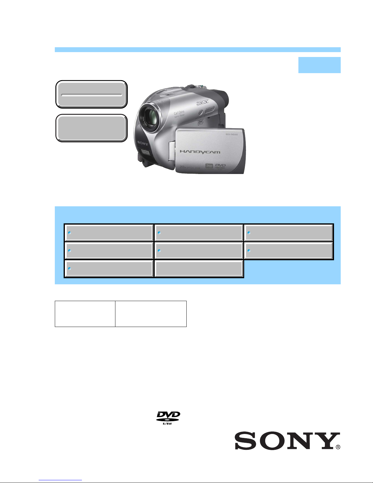
DIGITAL VIDEO CAMERA RECORDER
Photo: DCR-DVD105
The components identified by
mark 0 or dotted line with
mark 0 are critical for safety.
Replace only with part number specified.
Les composants identifiés par une
marque 0 sont critiques pour la
sécurité.
Ne les remplacer que par une pièce
portant le numéro spécifié.
2005L0500-1
© 2005.12
Published by DI Technical Support Department
9-876-924-31
US Model
Canadian Model
AEP Model
UK Model
East European Model
North European Model
E Model
Australian Model
Hong Kong Model
Chinese Model
Korea Model
Argentine Model
Brazilian Model
DCR-DVD105/DVD105E/
DVD605/DVD605E

— 2 —
DCR-DVD105/DVD105E/DVD605/DVD605E_L2
SPECIFICATIONS
These specifications are extracted from instruction
manual of DCR-DVD105E/DVD605E.
System
Video compression format
MPEG2/JPEG (Still images)
Audio compression format
Dolby Digital 2ch
Dolby Digital Stereo Creator
Video signal
PAL color, CCIR standards
Usable discs
8cm DVD-R/DVD-RW/DVD+RW
Recording format
Movie
DVD-R: DVD-VIDEO
DVD-RW: DVD-VIDEO (VIDEO mode),
DVD-Video Recording
(VR mode)
DVD+RW:DVD+RW Video
Still image
Exif
*1
Ver.2.2
Recording/playback time
HQ:Approx. 20 min
SP: Approx. 30 min
LP: Approx. 60 min
Viewfinder
Electric viewfinder
color
Image device
3 mm (1/6 type) CCD (Charge Coupled Device)
Gross:
Approx. 800 000 pixels
Effective (Movie):
Approx. 400 000 pixels
Effective (Still):
Approx. 400 000 pixels
Lens
Carl Zeiss Vario-Tessar
Filter diameter: 25mm (1 in.)
Optical:20×, Digital:40×, 800×
F=1.8-3.1
Focal length
f=2.3 - 46mm (3/32 - 1 13/16 in.)
When converted to a 35 mm still camera
For movies:
44 - 880mm (1 3/4 - 34 1/32 in.)
For still images:
44 - 880mm (1 3/4 - 34 1/32 in.)
Color temperature
[AUTO], [ONE PUSH], [INDOOR] (3 200 K),
[OUTDOOR] (5 800 K)
Minimum illumination
5 lx (lux) (F1.8)
0 lx (lux) (in the NightShot plus function)
*2
*1
“Exif” is a file format for still images, established
by the JEIT A (Japan Electronics and Information
Technology Industries Association). Files in this
format can have additional information such as
your camcorder’s setting information at the time
of recording.
*2
Objects unable to be seen due to the dark can be
shot with infrared lighting.
•Manufactured under license from Dolby
Laboratories.
Input/Output connectors
Audio/Video output
10 pin connector
Video signal: 1 Vp-p, 75 Ω (ohms), unbalanced
Luminance signal: 1 Vp-p, 75 Ω (ohms),
unbalanced
Chrominance signal: 0.3 Vp-p, 75 Ω (ohms),
unbalanced
Audio signal: 327 mV (at Load impedance
47 kΩ (kilohms)), Output impedance less than
2.2 kΩ (kilohms)
LCD screen
Picture
6.2 cm (2.5 type)
Tot al number of pixels
123 200 (560 × 220)
General
Power requirements
7.2 V (battery pack)
8.4 V (AC Adaptor)
Average power consumption
During camera recording using LCD
Viewfinder
Operating temperature
0°C to + 40°C (32°F to 104°F)
Storage temperature
-20°C to + 60°C (-4°F to + 140°F)
Dimensions (Approx.)
54 × 88 × 129mm (2 1/4 × 3 1/2 × 5 1/8 in.)
(w × h × d)
Mass (Approx.)
380 g (13 oz) main unit only
430 g (15 oz) including the NP-FP50
rech
AC Adaptor (1)
Mains lead (1)
A/V connecting cable (1)
Rechargeable battery pack
NP-FP50 (1)
Cleaning cloth (1)
Lens cap (1)
Operating Guide (This manual) (1)
argeable battery pack and disc
Supplied accessories
AC Adaptor AC-L25A/L25B
Power requirements
AC 100 - 240 V, 50/60 Hz
Current consumption
0.35 - 0.18 A
Power consumption
18W
Output voltage
DC 8.4V*
Operating temperature
0°C to + 40°C (32°F to 104°F)
Storage temperature
-20°C to + 60°C (-4°F to + 140°F)
Dimensions (Approx.)
56 × 31 × 100 mm (2 1/4 × 1 1/4 × 4 in.)
(w × h × d) excluding the projecting parts
Mass (Approx.)
190 g (6.7 oz) excluding the mains lead
* See at the label of AC Adaptor for other
specifications.
Rechargeable battery pack NP-FP50
Maximum output voltage
DC8.4V
Output voltage
DC7.2V
Capacity
4.9 wh (680 mAh)
Dimensions (Approx.)
31.8 × 18.5 × 45.0 mm
(1 5/16 × 3/4 × 1 13/16 in.) (w× h×d)
Mass (Approx.)
40 g (1.5 oz)
Operating temperature
0°C to + 40°C (32°F to 104°F)
Typ e
Li-ion
Design and specifications are subject to change
without notice.

— 3 —
DCR-DVD105/DVD105E/DVD605/DVD605E_L2
Model information table
•Abbreviation
AR : Argentine model
AUS: Australian model
BR : Brazilian model
CH : Chinese model
CND: Canadian model
EE : East European model
HK : Hong Kong model
JE : Tourist model
KR : Korea model
MX : Mexican Model
NE : North European model
Model DCR-DVD105 DCR-DVD105E DVR-DVD605 DCR-DVD605E
Destination US, CND, E, AR, BR AEP, UK, NE, EE E, KR E, HK, AUS, CH
Color system NTSC PAL NTSC PAL
— 4 —
DCR-DVD105/DVD105E/DVD605/DVD605E_L2
1. Check the area of your repair for unsoldered or poorly-soldered
connections. Check the entire board surface for solder splashes
and bridges.
2. Check the interboard wiring to ensure that no wires are
"pinched" or contact high-wattage resistors.
3. Look for unauthorized replacement parts, particularly
transistors, that were installed during a previous repair . Point
them out to the customer and recommend their replacement.
4. Look for parts which, through functioning, show obvious signs
of deterioration. Point them out to the customer and
recommend their replacement.
5. Check the B+ voltage to see it is at the values specified.
6. Flexible Circuit Board Repairing
•Keep the temperature of the soldering iron around 270˚C
during repairing.
• Do not touch the soldering iron on the same conductor of the
circuit board (within 3 times).
• Be careful not to apply force on the conductor when soldering
or unsoldering.
SAFETY CHECK-OUT
After correcting the original service problem, perform the following
safety checks before releasing the set to the customer.
Unleaded solder
Boards requiring use of unleaded solder are printed with the leadfree mark (LF) indicating the solder contains no lead.
(Caution: Some printed circuit boards may not come printed with
the lead free mark due to their particular size.)
: LEAD FREE MARK
Unleaded solder has the following characteristics.
• Unleaded solder melts at a temperature about 40°C higher than
ordinary solder.
Ordinary soldering irons can be used but the iron tip has to be
applied to the solder joint for a slightly longer time.
Soldering irons using a temperature regulator should be set to
about 350°C.
Caution: The printed pattern (copper foil) may peel away if the
heated tip is applied for too long, so be careful!
• Strong viscosity
Unleaded solder is more viscous (sticky, less prone to flow) than
ordinary solder so use caution not to let solder bridges occur such
as on IC pins, etc.
• Usable with ordinary solder
It is best to use only unleaded solder but unleaded solder may
also be added to ordinary solder.
SAFETY-RELATED COMPONENT WARNING!!
COMPONENTS IDENTIFIED BY MARK 0 OR DOTTED LINE WITH
MARK 0 ON THE SCHEMATIC DIAGRAMS AND IN THE PARTS
LIST ARE CRITICAL TO SAFE OPERATION. REPLACE THESE
COMPONENTS WITH SONY PARTS WHOSE PART NUMBERS
APPEAR AS SHOWN IN THIS MANUAL OR IN SUPPLEMENTS
PUBLISHED BY SONY .
ATTENTION AU COMPOSANT AYANT RAPPORT
À LA SÉCURITÉ!
LES COMPOSANTS IDENTIFÉS P AR UNE MARQUE 0 SUR LES
DIAGRAMMES SCHÉMA TIQUES ET LA LISTE DES PIÈCES SONT
CRITIQUES POUR LA SÉCURITÉ DE FONCTIONNEMENT. NE
REMPLACER CES COMPOSANTS QUE PAR DES PIÈSES SONY
DONT LES NUMÉROS SONT DONNÉS DANS CE MANUEL OU
DANS LES SUPPÉMENTS PUBLIÉS PAR SONY.
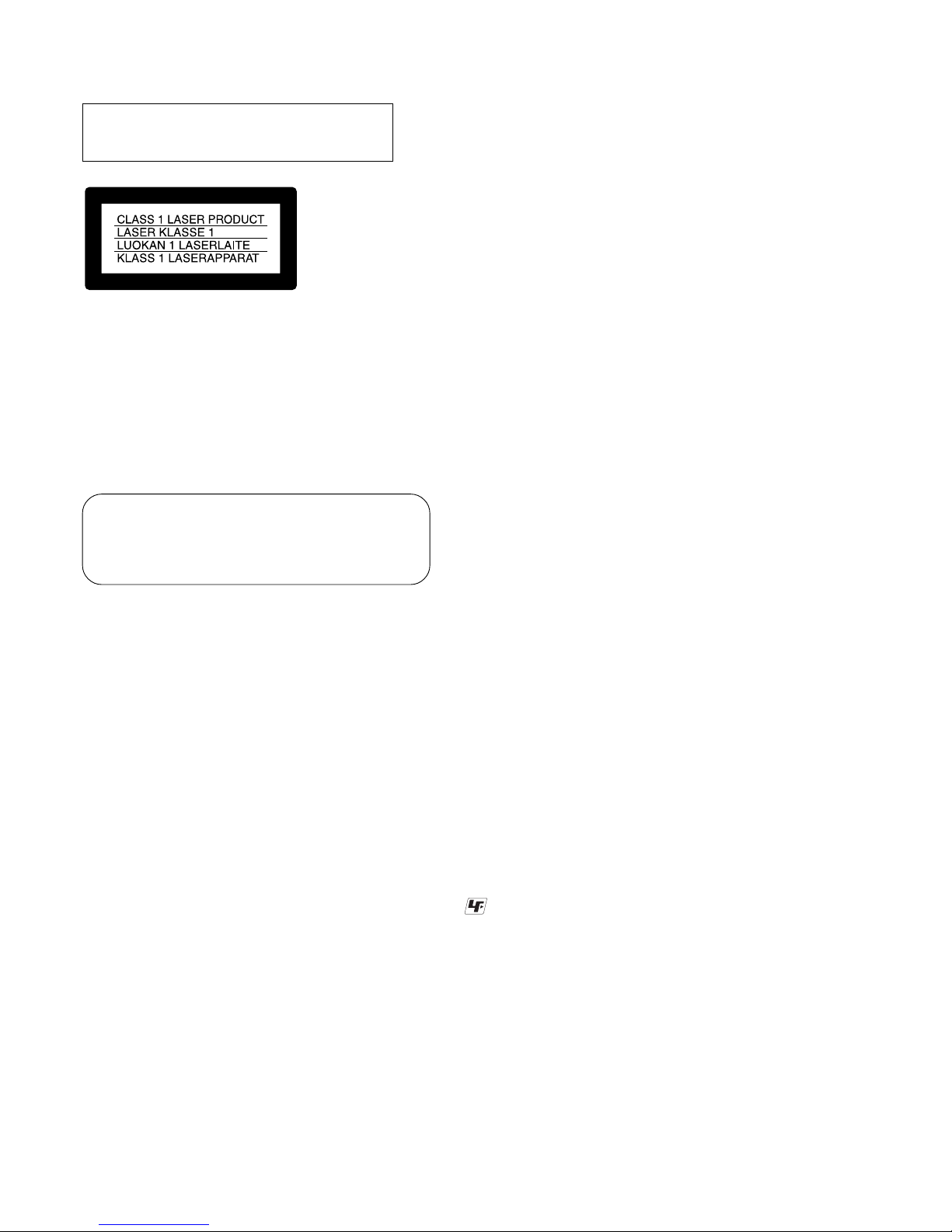
WARNING!!
WHEN SERVICING, DO NOT APPROACH THE LASER
EXIT WITH THE EYE TOO CLOSELY. IN CASE IT IS
NECESSARY TO CONFIRM LASER BEAM EMISSION,
BE SURE TO OBSER VE FR OM A DIST ANCE OF MORE
THAN 30 cm FROM THE SURFACE OF THE
OBJECTIVE LENS ON THE OPTICAL PICK-UP BLOCK.
CAUTION:
The use of optical instrument with this product will increase eye
hazard.
CAUTION :
Danger of explosion if battery is incorrectly replaced.
Replace only with the same or equivalent type.
CAUTION
Use of controls or adjustments or performance
procedures other than those specified herein may
result in hazardous radiation exposure.

— 5 —
DCR-DVD105/DVD105E/DVD605/DVD605E_L2
TABLE OF CONTENTS
1. SERVICE NOTE
1-1. Power Supply During Repairs········································· 1-1
1-2. To Take Out a Disc when not Eject (Force Eject) ···········1-1
1-3. Setting The “Forced Power On” Mode····························1-1
1-4. Using Service Jig·····························································1-2
1-5. Self-diagnosis Function ···················································1-2
1-6. Precaution on Replacing The VC-421 Board ··················1-4
2. DISASSEMBLY
2-1. Disassembly·····································································2-2
3. BLOCK DIAGRAMS
3-1. Overall Block Diagram (1/5)···········································3-1
3-2. Overall Block Diagram (2/5)···········································3-3
3-3. Overall Block Diagram (3/5)···········································3-5
3-4. Overall Block Diagram (4/5)···········································3-7
3-5. Overall Block Diagram (5/5)···········································3-9
3-6. Power Block Diagram (1/3)··········································· 3-11
3-7. Power Block Diagram (2/3)··········································· 3-13
3-8. Power Block Diagram (3/3)··········································· 3-15
4. PRINTED WIRING BOARDS AND
SCHEMATIC DIAGRAMS
4-1. Schematic Diagrams························································4-1
4-2. Printed Wiring Boards ···················································4-51
4-3. Waveforms ·····································································4-73
4-4. Mounted Parts Location ················································4-79
5. REPAIR PARTS LIST
5-1. Exploded V iews ·······························································5-2
5-2. Electrical Parts List························································5-12
Section Title Page
1-1
DCR-DVD105/DVD105E/DVD605/DVD605E_L2
1. SERVICE NOTE
1-1. POWER SUPPLY DURING REPAIRS
In this unit, about 10 seconds after power is supplied to the battery terminal using the regulated power supply (8.4V), the po wer is shut of f so
that the unit cannot operate.
These following method is available to prevent this.
Method:
Use the AC power adaptor (AC-L25A/L25B).
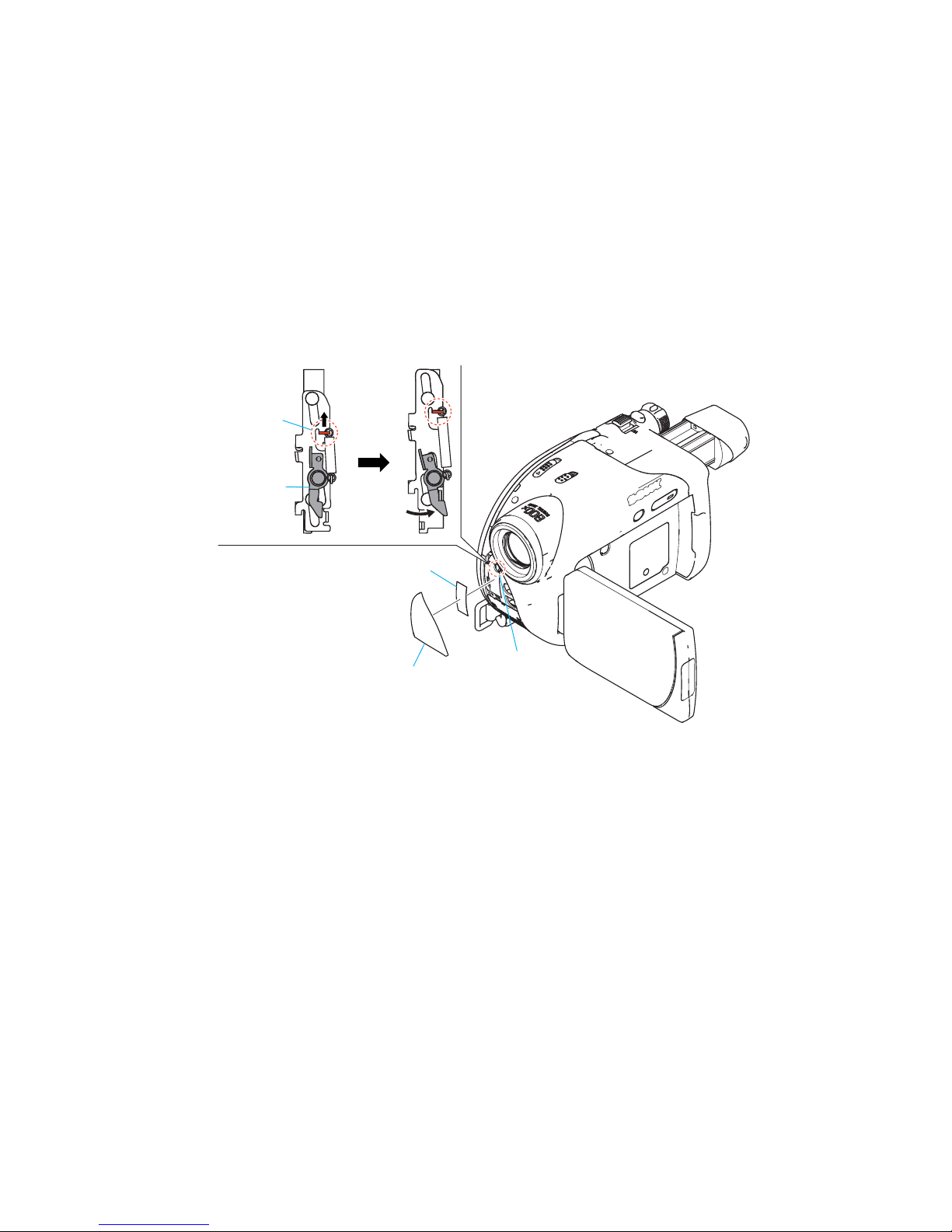
1-2. TO TAKE OUT A DISC WHEN NOT EJECT (FORCE EJECT)
1 Peel off the remote control window and remote control window sheet.
2 Insert the wire etc. in the hole and lift the eject slider by it.
Eject slider
Remote control window
Remote control window sheet
Hole
Eject charge
lever
1-3. SETTING THE “FORCED POWER ON” MODE
It is possible to turn on power by adjustment remote commander (RM-95 or NEW LANC JIG).
Operate the camcorder using the adjustment remote commander.
1-3-1. Setting the “Forced Movie Power ON” Mode
1) Select page: 0, address: 01, and set data:01.
2) Select page: A, address: 10, set data:01 and press the “PAUSE (Write)” button of the adjustment remote commander.
1-3-2. Setting the “Forced Play/Edit Power ON” Mode
1) Select page: 0, address: 01, and set data:01.
2) Select page: A, address: 10, set data:02 and press the “PAUSE (Write)” button of the adjustment remote commander.
1-3-3. Exiting the “Forced Power ON” Mode
1) Select page: 0, address: 01, and set data:01.
2) Select page: A, address: 10, set data:00 and press the “PAUSE (Write)” button of the adjustment remote commander.
3) Select page: 0, address: 01, and set data: 00.
1-2
DCR-DVD105/DVD105E/DVD605/DVD605E_L2
1-5. SELF-DIAGNOSIS FUNCTION
1-5-1. Self-diagnosis Function
When problems occur while the unit is operating, the self-diagnosis
function starts working, and displays on the viewfinder or LCD
screen what to do. This function consists of two display; selfdiagnosis display and service mode display.
Details of the self-diagnosis functions are provided in the Instruction
manual.
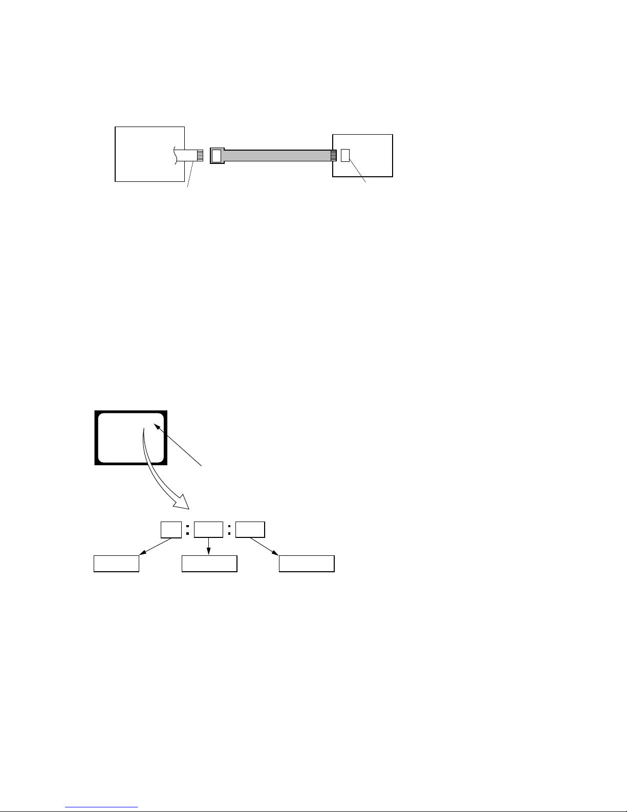
1-5-2. Self-diagnosis Display
When problems occur while the unit is operating, the counter of the
viewfinder or LCD screen shows a 4-digit display consisting of an
alphabet and numbers, which blinks at 3.2 Hz. This 5-character
display indicates the “repaired by:”, “block” in which the problem
occurred, and “detailed code” of the problem.
1 1
3 1C
Repaired by:
Refer to “1-5-3. Self-diagnosis Code Table”.
Indicates the appropriate
step to be taken.
E.g.
31 ....Reload the tape.
32 ....Turn on power again.
Block
Detailed Code
Blinks at 3.2Hz
C : Corrected by customer
H : Corrected by dealer
E : Corrected by service
engineer
Viewfinder or LCD screen
C : 3 1 : 1 1
DVD mechanism deck
VC-421 board (side B
)
Flexible board
(from DVD mechanism deck (10P))
Extension cable (10P)
(J-6082-572-A)
CN1009
1-4. USING SERVICE JIG
Connect the extension cable (J-6082-572-A) between the DVD mechanism deck and CN1009 on the VC-421 board.

1-3
DCR-DVD105/DVD105E/DVD605/DVD605E_L2
1-5-3. Self-diagnosis Code Table
C
C
C
C
C
E
E
E
E
E
E
E
E
E
E
E
Block
Function
04
13
13
21
32
20
31
40
40
61
61
61
62
62
94
94
Detailed
Code
00
00
02
00
50
00
00
00
01
00
10
11
00
01
00
01
Symptom/State
Non-standard battery is used.
Faulty disc is used.
Disc access error
Condensation.
Codec IC dose not return are reply
EEPROM data are rewritten.
Drive fault
Codec IC fault
Audio Codec IC fault
Difficult to adjust focus
(Cannot initialize focus.)
Zoom operations fault
(Cannot initialize zoom lens.)
The abnormalities in initialization of
the focus lens and the abnormalities in
initialization of the zoom lens occurred
simultaneously.
Handshake correction function does not
work well. (With PITCH angular
velocity sensor output stopped.)
Handshake correction function does not
work well. (With YAW angular velocity
sensor output stopped.)
Fault of writing to or erasing the flash
memory
Fault of writing to or erasing EEPROM
Self-diagnosis Code
Repaired by:
Correction
Use the InfoLITHIUM battery.
Use a compatible disc with the camcorder.
Clean the disc with the supplied cleaning cloth.
Use a compatible disc with the camcorder.
Remove the disc, and insert it again after one hour.
Remove the power source. Reconnect it again and operate your
camcorder again
Make EEPROM data correct value. (Note)
Inspect or replacement of the mechanism deck, IC (IC4302 on
the VC-421 board) and drive block
Inspect or replacement of the codec IC (IC3001on the VC-421
board) peripheral circuits
Inspect or replacement of the Audio Codec IC (IC3001 on the
VC-421 board) peripheral circuits
Inspect the lens block focus reset sensor (pin ql of CN1301 on
the VC-421 board) when focusing is performed when the touch
panel is operated in the focus manual mode and the focus motor
drive circuit (IC1301on the VC-421 board) when the focusing is
not performed.
Inspect the lens block zoom reset sensor (pin qg of CN1301 on
the VC-421 board) when zooming is performed when the zoom
switch is operated and the zoom motor drive circuit (IC1301on
the VC-421 board) when zooming is not performed.
Check whether the flexible board of the lens is broken, and
check whether it is inserted imperfectly. If there is no problem in
the flexible board, inspect the focus/zoom motor drive circuit
(IC1301 on the VC-421 board).
Inspect PITCH angular velocity sensors (SE6302 on the MA-440
board) peripheral circuits.
Inspect YAW angular velocity sensors (SE6301 on the MA-440
board) peripheral circuits.
Inspect the flash memory (IC3101 on the VC-421 board). (Note)
Inspect the EEPROM (IC2602 on the VC-421 board). (Note)
Note: Refer to “7-2. Record of Self-diagnosis check” of “3-5. SERVICE MODE”, ADJ (9-876-924-51).

1-4E
DCR-DVD105/DVD105E/DVD605/DVD605E_L2
1-6. PRECAUTION ON REPLACING THE VC-421 BOARD
Exif Model Data Check
When you replace to the repairing board, the written data of repairing board also might be changed to original setting.
When the data has changed because of board replaceing etc, check the data setting (Exif Model Data) is right. If not, rewrite to the right v alue.
Exif Model Data
Writing Method:
1) Select page: 0, address: 01 and set data: 01.
2) Select page: A, address: B7 to BA, and set the Exif Model Data.
Note: To write in the non-volatile memory (EEPROM), press the PAUSE (Write) button each time to set the data.
3) Select page: 0, address: 01, and set data: 00.
Page
A
A
A
A
Data
DCR-DVD105
31
30
35
00
DCR-DVD605
36
30
35
00
DCR-DVD105E
31
30
35
45
DCR-DVD605E
36
30
35
45
Address
B7
B8
B9
BA

2-1
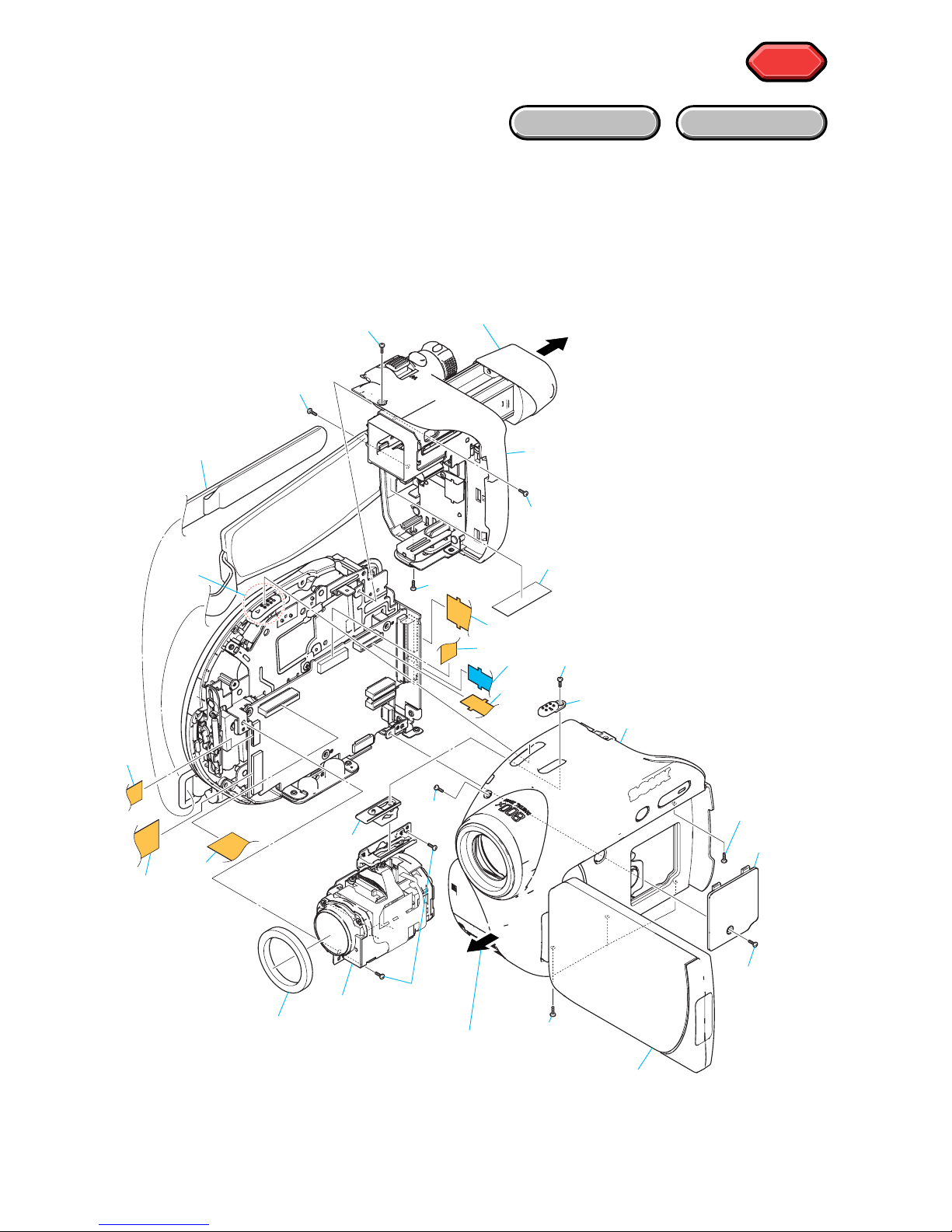
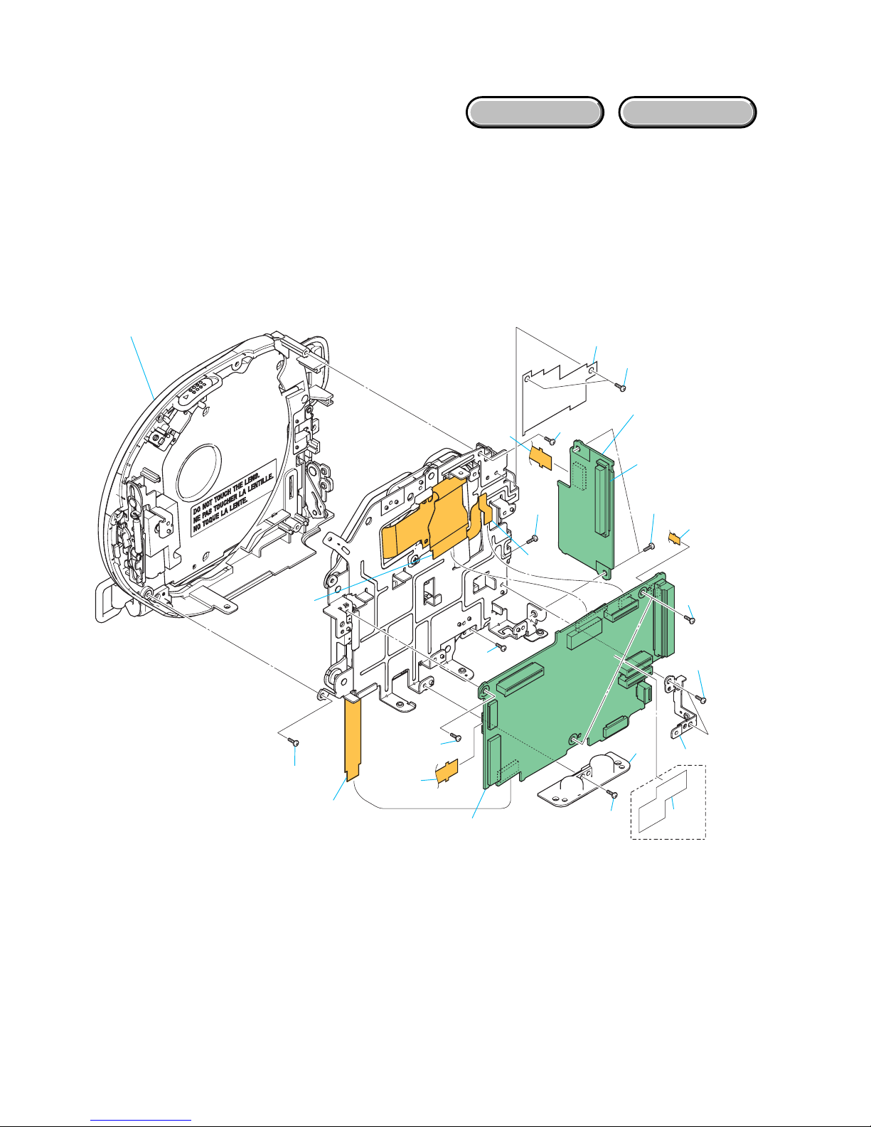
2. DISSASSEMBLY
DCR-DVD105/DVD105E/DVD605/DVD605E_L2
Cut and remove the part of gilt
which comes off at the point.
(Be careful or some
pieces of gilt may be left inside)
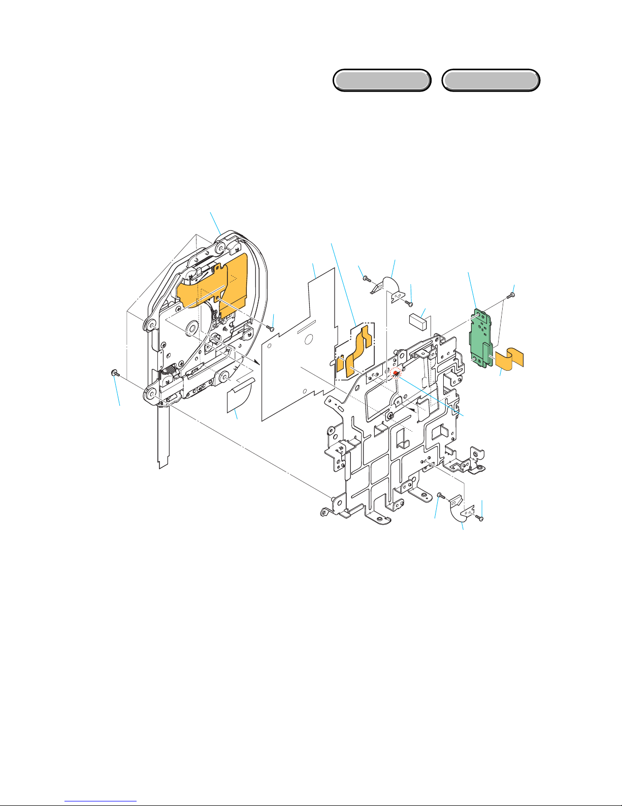
NOTE FOR REPAIR
• Make sure that the flat cable and flexible board are not cracked of bent at the terminal.
Do not insert the cable insufficiently nor crookedly.
• When remove a connector, dont’ pull at wire of connector. It is possible that a wire is snapped.
• When installing a connector, dont’ press down at wire of connector.
It is possible that a wire is snapped.
2-2
DCR-DVD105/DVD105E/DVD605/DVD605E_L2
2-1. DISASSEMBLY
2-1-1. OVERALL ASSEMBLY
HELP
HELP
2-5 (#3)
2-7 (#2)
2-6 (#2)
2-4
(Slide the EVF)
2-2
2-1
2-3
2-8
2-9
3-3 (#2)
3-2
3-1
3-4
2 BT Cabinet Block
3 Lens Block
1 Cabinet (R) block
1-1 (#4)
1-11
1-14
1-13
1-12
1-4 (#2)
1-9 (#2)
1-8 (#2)
1-7
(#10)
1-5 (#1)
1-3 (Open the LCD)
1-10
(Slide the cabinet (R) block)
1-2
1-6
EXPLODE VIEW
HARDWARE LIST
2-3
DCR-DVD105/DVD105E/DVD605/DVD605E_L2
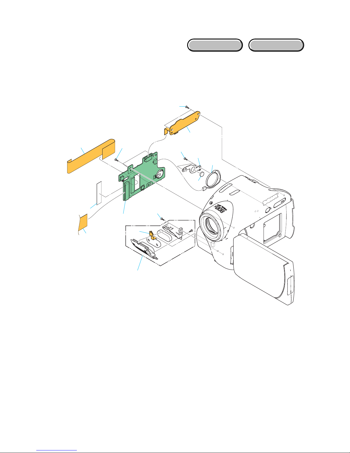
2-1-2. CABINET (R) BLOCK-1
CK-154
1 Mic block
2 CK-154 board
1-2 (#9)
1-1
2-5 (#5)
2-6 (#5)
2-7
2-8
2-10
2-2 (#5)
2-3
2-4
2-1
2-9
EXPLODE VIEW
HARDWARE LIST
2-4
DCR-DVD105/DVD105E/DVD605/DVD605E_L2
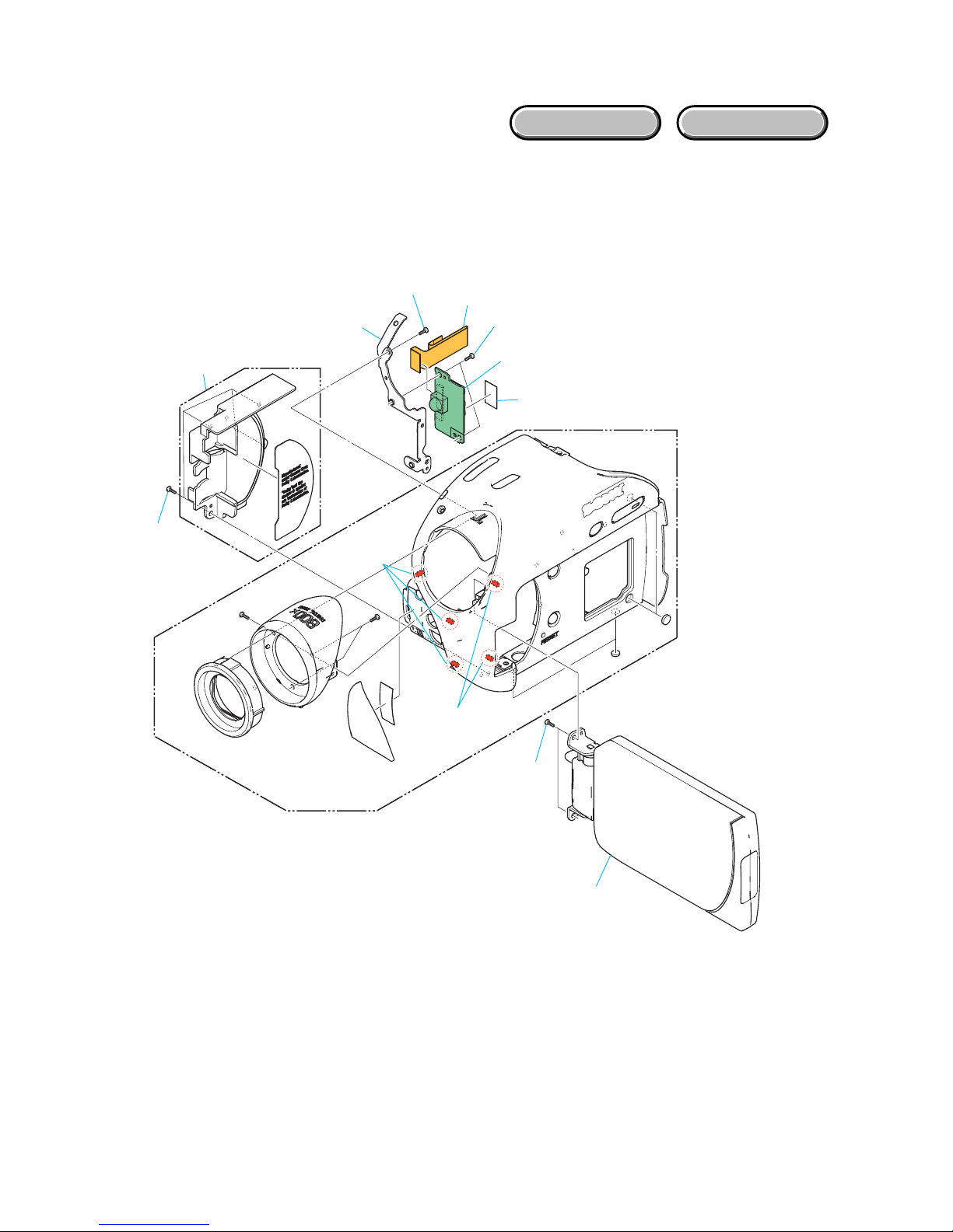
2-1-3. CABINET (R) BLOCK-2
MA-440
1 MA-440 board
2 LCD block
1-1 (#9)
1-3
1-5
1-6
1-2
(Boss)
1-4 (#3)
2-1 (#5)
2-3 (#9)
2-4 (Boss)
2-2
EXPLODE VIEW
HARDWARE LIST
2-5
DCR-DVD105/DVD105E/DVD605/DVD605E_L2
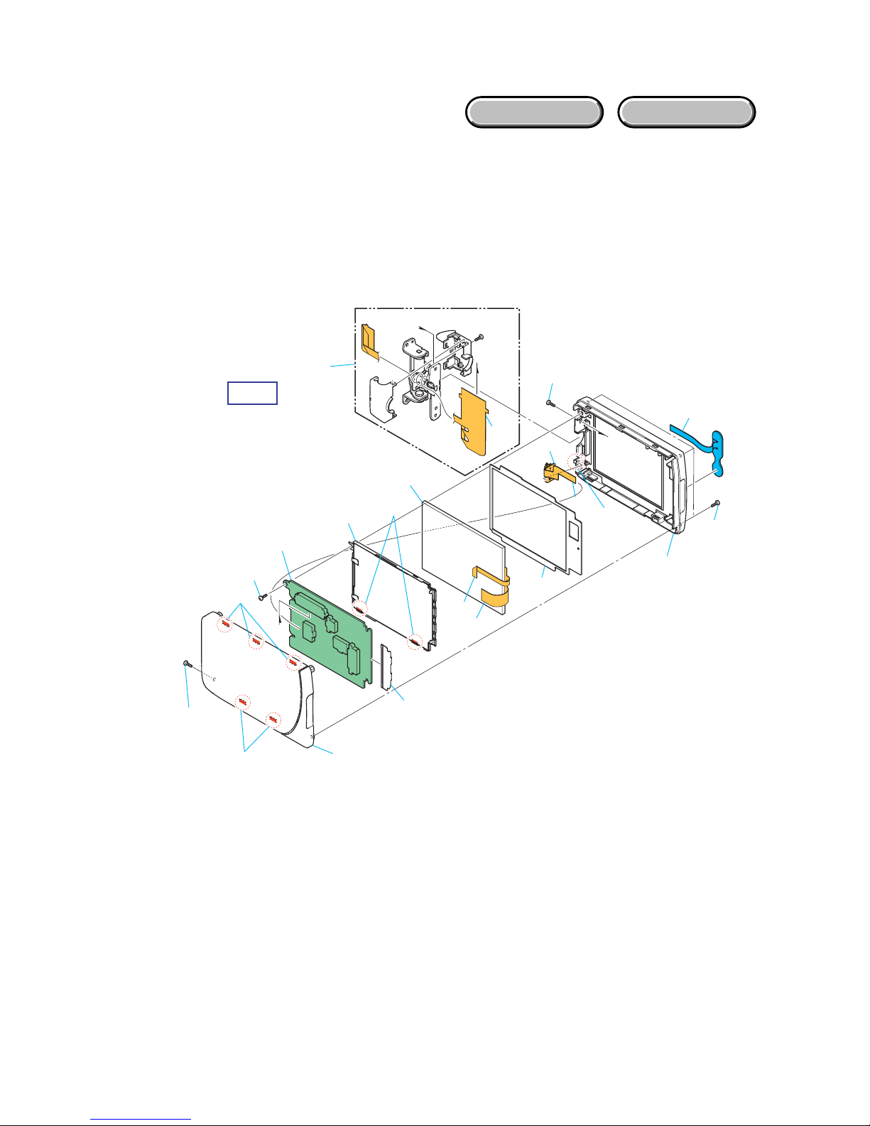
2-1-4. LCD BLOCK
HELP
PD-267
3-1
3-2
1 Hinge block
3 LCD
2 PD-267 board
1-1 (#5)
1-2 (#2)
1-10 (#2)
1-5
1-3 (Claw)
1-4 (Claw)
1-7
(Claw)
1-8
1-6
A
A
B
B
1-9
2-1
2-2
2-3
2-6
2-7
2-4 (#5)
2-5
(Claw)
EXPLODE VIEW
HARDWARE LIST
2-6
DCR-DVD105/DVD105E/DVD605/DVD605E_L2
2-1-5. MAIN BLOCK-1
VC-421
DD-246
2-2
2-4
3-1
(#3)
3-4 (#5)
3-2 (#5)
3-3 (#5)
3 Cabinet (L) block
1 DD-246 board
2 VC-421 board
1-1 (#3)
1-2
(Connector)
1-3
2-1 (#3)
2-3 (#3)
2-7 (#3)
2-8 (#3)
2-9
2-10
2-11
2-12
2-13
2-14
2-5 (#2)
2-6
US, CND
EXPLODE VIEW
HARDWARE LIST
2-7E
DCR-DVD105/DVD105E/DVD605/DVD605E_L2
2-1-6. MAIN BLOCK-2
JK-298
3-1
1 JK-298 board
3 FP-342 flexible board
2 Optical drive
1-1 (#3)
2-1 (#6)
2-9
2-3 (#6)
2-4 (#7)
2-5
2-2 (Boss)
1-2
2-10
2-11
2-6 (#6)
2-7 (#7)
2-8
EXPLODE VIEW
HARDWARE LIST
HELP
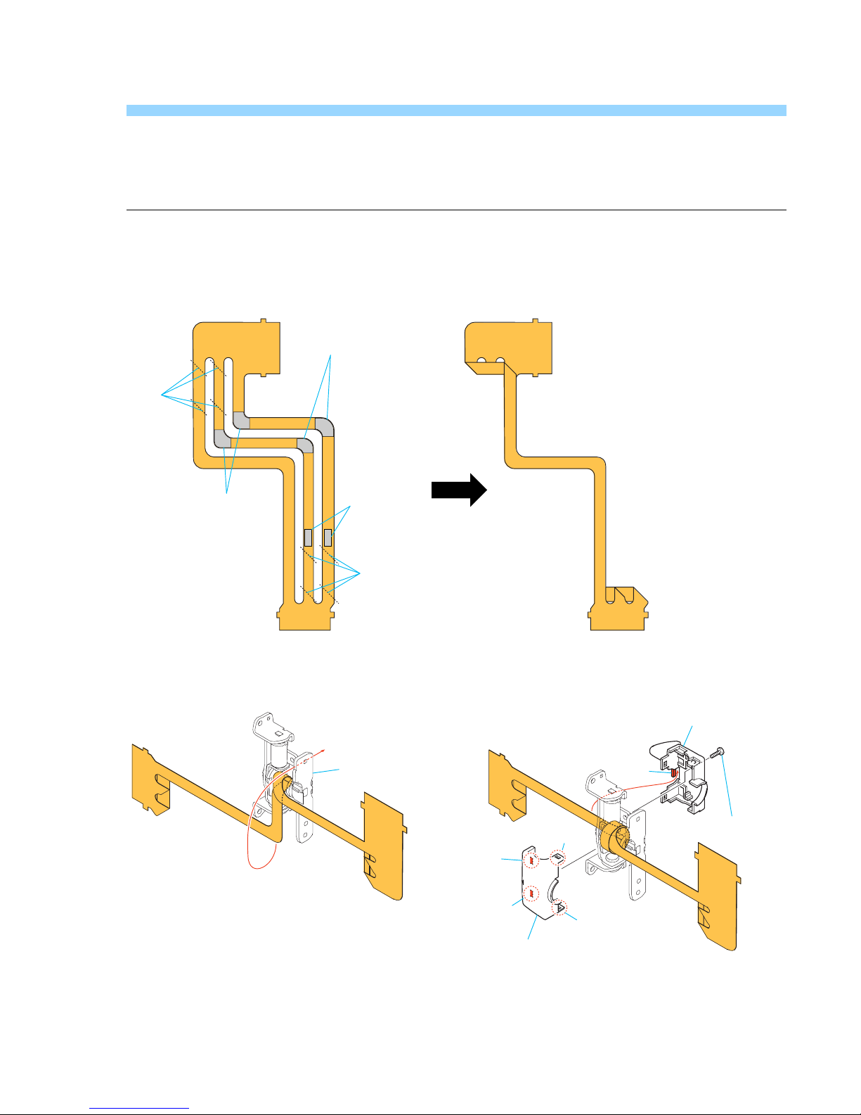
DCR-DVD105/DVD105E/DVD605/DVD605E_L2
HELP
Sheet attachment positions and procedures of processing the flexible boards/harnesses are shown.
Fold
Hinge cover (C)
Screw (#1)
Hinge cover (M)
Claw
Hinge assy
Adhesive tape
Adhesive tape
Adhesive tape
1 Fold dotted line parts of the FP-340 flexible board
as shown in figure.
2 Roll the the FP-340 flexible board 1.5 times,
in the direction of arrow
A.
3 Attach two hinge covers as shown in fugure.
A
Fold
Claw
Claw
Claw
Claw
THE METHOD OF ATTACHMENT OF FP-340 FLEXIBLE BOARD

DCR-DVD105/DVD105E/DVD605/DVD605E_L2
Link
Link
3. BLOCK DIAGRAMS
OVERALL BLOCK DIAGRAM (2/5)
OVERALL BLOCK DIAGRAM (1/5) OVERALL BLOCK DIAGRAM (5/5)
POWER BLOCK DIAGRAM (1/3)
OVERALL BLOCK DIAGRAM (3/5)
POWER BLOCK DIAGRAM (2/3)
OVERALL BLOCK DIAGRAM (4/5)
POWER BLOCK DIAGRAM (3/3)
DCR-DVD105/DVD105E/DVD605/DVD605E_L2
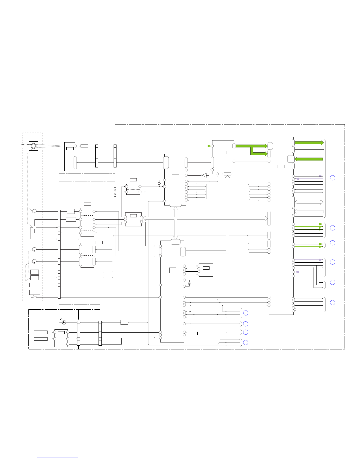
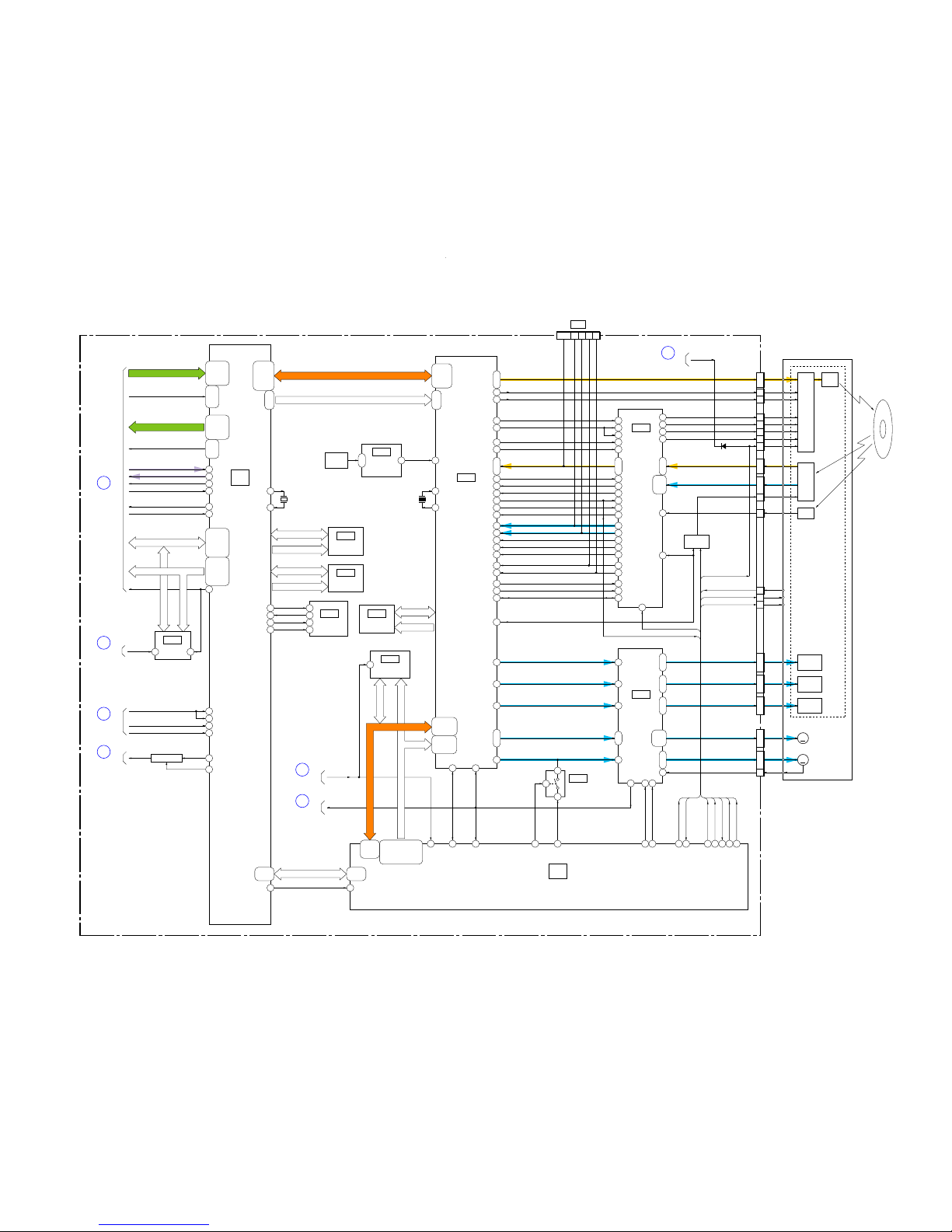
3-1. OVERALL BLOCK DIAGRAM (1/5)
3-1 3-2
( ) : Number in parenthesis ( ) indicates the division number of schematic diagram where the component is located.
3. BLOCK DIAGRAMS
CAMERA SIGNAL
PROCESS,
VIDEO/AUDIO DSP,
LENS CONTROL
(5/14)
IC2701
SE6301
SE6302
YAW_AD
PITCH_AD
PITCH SENSOR
YAW SENSOR
PITCH/YAW
SENSOR
AMP
8
12
2
18
19
IC6302
30
TIMING
GENERATOR
(1/14)
IC1201
S/H, AGC,
A/D CONVERTER
(2/14)
IC1101
26, 25, 28, 31,
18, 21, 22, 33
42
16
43
CN6001
CD-600 BOARD FP-333
FLEXIBLE
BOARD
FP-341 FLEXIBLE
BOARD (1/2)
VC-421 BOARD (1/5)
V1 - V4, RG,
H1, H2, VSHT
V1 - V4, RG,
H1, H2, VSHT
7
CCD
IMAGER
IRIS
(SHUTTER)
LENS BLOCK
CCD_OUTCCD_OUT
CCD_OUT
IC6001
1 - 4, 9, 12, 13, 10
CLAMP
Q6001
LED
DRIVE
Q1001
2 - 11
1, 2, 15, 16
23, 19, 21, 22
15
MA-440 BOARD (1/2)
CN6302
(1/2)
16
VST_C_RESET
15
14
NS_LED_K
7
CN1002
(1/2)
1
3
10
2
LENS_TEMP_AD
05
AC9,
Y9, Y6
OVERALL (2/5)
(PAGE 3-3)
1
OVERALL (4/5)
(PAGE 3-7)
3
OVERALL (4/5)
(PAGE 3-7)
4
OVERALL (2/5)
(PAGE 3-3)
5
OVERALL (3/5)
(PAGE 3-5)
2
OVERALL (5/5)
(PAGE 3-9)
8
OVERALL (3/5)
(PAGE 3-5)
11
248, 250, 251 239, 246, 247
268 - 270
3 - 10
279 - 282
264 - 267,
272, 273,
275, 276
224 - 231,
233, 234
116 - 98 137 - 124, 122, 121
141
241
219
220
217
EN0,
DIR0A, DIR0B
EN01,
DIR1A, DIR1B
ZM_RST
FC_RST
DA_STRB
IRIS_PWM, IRIS_COM
IRIS_PWM, IRIS_COM
I_HALL_AD
TG_FLD TG_FLD
I_HALL_AD
238
237
ZOOM_VR_AD
P22
P23
IR_ON
A13
R22
Y5
P20
Y18
IR_ON
T2
11 - 8, 3 - 1, 6
CN1201
15
XSYS_RST
OVERALL (3/5)
(PAGE 3-5)
9
XRST_VTR
163
CAM_DD_ON
CAM_DD_ON
XSYS_RST
ZOOM_VR_AD
XSYS_RST
XSYS_RST
216
222
236
159, 158, 156, 154, 162
D6302
(NIGHTSHOT)
47, 48, 46
35, 38, 37, 39
AD0 - AD9
AD0 - AD9
AD0 - AD9
D0 - D9
CAMERA
CONTROL
(4/14)
IC2601
(1/2)
F2
157
SYS_V
164
M22
SYS_V
LINEOUT_V
D14
F4
AB19
D13
XRST_VTR
11 - 8, 3 - 1, 6
ED0 - ED7
ADATAIN0
ADATAOUT0
HYI_PLL27IN
MPLCK27
252 - 261
CAM_SO, CAM_SCK
CAM_SI, CAM_SO,
CAM_SCK,
CAM_CS, CAM_VD
CAM_SI, CAM_SO,
CAM_SCK, CAM_CS
CAM_SI, CAM_SO, CAM_SCK, CAM_CS, CAM_VD
EN0,
DIR0A, DIR0B
EN01,
DIR1A, DIR1B
ZM_RST
FC_RST
AB11, Y11,
AB10, C22, A7
A1_CNM - A19_CNM
D0_CNM - D15_CNM
301
298
284
304
119
87
85
82
83
XNS_SW
LENS_TEMP_AD
XNS_SW
CH_SO, CH_SCK, CH_CS
CH_SO, CH_SCK, CH_CS
LINEOUT_V
SYS_V
LINEOUT_V
B8
A9
OVERALL (2/5)
(PAGE 3-3)
10
SPDL_FG
SPDL_FG
OSC1
DSCK_CNM
53
60
IC_2701_Y_OUT
IC_2701_C_OUT
DATA_TO_SFD
89
DATA_FROM_SFD
40
39
PANEL_R
PANEL_G
45
PANEL_B
92
PANEL_XHD
93
PANEL_XVD
161
LINEIN_VD
149
MCXCS_IC_2701
152
BB_SI
151
BB_SO
150
XBB_SCK
144
CNMXCS_IC_2701
147
JAIRQ
SFD_BCK
SFD_LRCK
SFD_FCK
91
KASYAON
A : VIDEO SIGNAL
A : AUDIO SIGNAL
OVERALL (4/5)
(PAGE 3-8)
6
RYO0_DEHD, RYO1_DEVD,
RYO2_DEFLD
RCO0_EDHD, RCO1_EDVD,
RCO2_EDFLD, RCO3_FRMREF
RYI0_DE0 - RYI3_DE3
RCI0_DE4 - RCI3_DE7
F1
AB13
AC14
AB14
1
6
5
2
32K EEPROM
(4/14)
IC2602
EEP_SI
EEP_SO
EEP_SCK
XCS_EEP
X2601
20MHz
D1
C1
40
11
34
44
45
41
48
36
CLPDM_TG, PBLK_TG,
XSHP, XSHD
SYSCK VCK
20
221
CLPOB
XRST_RST
Q1201
9
ADCK27
46
CKCONT2
TG_HD
TG_VD
ZSG1
ZV1
TG_ID
VGAT
VCK
TG_HD
TG_VD
ZSG1
ZV1
TG_ID
VGAT
IC3701
EVR
(D/A CONVERTER)
(3/14)
3
2
1 8
6, 7
Y16, AC17
H
M
IRIS
METER
M
FOCUS
SENSOR
ZOOM
SENSOR
FOCUS
MOTOR
ZOOM
MOTOR
M
CN1301
12
8
9
4 - 124 - 21
19
LENS TEMP
SENSOR
IRIS
DRIVE
Q1301
HALL GAIN
CONTROL
Q1303
NIGHTSHOT
PLUS
(3/14)
IRIS DRIVE
I_DRIVE (-)
I_BIAS (-)
6
I_BIAS (+)
I_HALL (-)
7
I_HALL (+)
FC_A, FC_XA,
FC_B, FC_XB
ZM_A, ZM_XA,
ZM_XB, ZM_B
FC_SENS_OUT
15
ZM_SENS_OUT
16
THERMO_OUT
17
NightShot_Vcc
HALL GAIN
IC1302
(3/14)
IC1301
FOCUS
MOTOR
DRIVE
ZOOM
MOTOR
DRIVE
5, 19, 17, 7 2, 23, 4, 21
14, 16, 13, 15 10, 12, 9, 11
8
14
HALL AMP
5 7
6
12
10
HALL BIAS
1
2
4
X1201
36MHz
5
XTAL AMP
A_2.8V
HALL VRefHALL REG
IC1303
(3/14)
FREQ_AMPOUT
75
3
1
DCR-DVD105/DVD105E/DVD605/DVD605E_L2
3-3 3-4
3-2. OVERALL BLOCK DIAGRAM (2/5) ( ) : Number in parenthesis ( ) indicates the division number of schematic diagram where the component is located.
A : VIDEO SIGNAL
A : AUDIO SIGNAL
A : VIDEO/AUDIO SIGNAL
A : VIDEO/AUDIO/SERVO SIGNAL
A : SERVO SIGNAL
DVD CODEC,
USB I/F
(6/14)
IC3001
(1/2)
DVD DSP
(8/14)
IC4101
CN1017
(FOR CHECK)CPC
DVD DRIVE CONTROL
(10/14)
IC4201
(1/2)
RF PROCESS
(9/14)
IC4001
DVD MECHA
DRIVE
(11/14)
IC4302
16M FLASH
(10/14)
IC4202
64M SDRAM
(8/14)
IC4102
LD
DRIVE
PD IC
FPD IC
LASER
DIODE
VC-421 BOARD (2/5)
DVD MECHANISM DECK
(DDX-C1002)
05
OVERALL (1/5)
(PAGE 3-2)
1
M4C7
AA21
AB21
AH23
AB20
V2
E10
D10
E11
1
6
2
5
AA22
Y22
ED0 - ED7
RYO0_DEHD, RYO1_DEVD,
RYO2_DEFLD
RCO0_EDHD, RCO1_EDVD,
RCO2_EDFLD, RCO3_FRMREF
RYI0_DE0 - RYI3_DE3
RCI0_DE4 - RCI3_DE7
ATA_A0 - ATA_A2
ADATAIN0
ADATAOUT0
HYI_PLL27IN
MPLCK27
H17, G14
A9, B9
L6, L7
B6, A7
A1_CNM - A19_CNM
A1_CNM - A23_CNM
D0_CNM - D15_CNM
ATA_D0 - ATA_D15
D0_CNM - D15_CNM
RFOP, RFON
FEO
TEO
VRCK
LVL
WBO
HDO
FLGA
AH20,
AE18,
AE19
D17,
B17,
E17
T10,
P10,
P11
45, 44,
48, 1
AD18,
AD17,
AB19,
AB18
AB9,
AD6 - AD9,
AE5 - AE9,
AG4 - AG10,
AH4 - AH9,
AA18, AE20,
AD20, AG20,
AB17, AG21,
AD19, AE22
AB15, AE17,
AA14, AB16,
AG17, AH19,
AA15, AG19
M13 - M15,
N15, N16,
P15, P16, R17
P14, R14, R15,
T14, T15,
U14 - U16
K16, L16, L17,
M15 - M17, N15 -N17,
P15 - P17, R10, R15 -R17
T8, T9, T15, U9, U10
R2 -R7,
T3 -T7,
U3 - U7
B10, A11,
C11, A9
G10, D11,
B11, U5
P4 - P7,
R4 - R7,
T3 -T7,
U3, U5, U7
A8 - A12,
B8 - B10
A13, A14,
B13 - B16,
D13 - D16,
E13 - E16,
G13, G14
AB11 - AB13,
AD10 - AD13,
AE11 - AE13,
AG11 - AG13,
AH11 - AH13
DSCK_CNM
SFD_FCK
U2
BEEP MELODY
MELODY_ENV
AC5
SFD_BCK
AD22
C1
AA20
SFD_LRCK
DSCK_CNM
12
5
10 9 8 7
1
16
17
14
15
2, 3
17, 19
27, 26
2
AD16
P5
CNMXCS_IC_2701
JAIRQ
Q4001,
Q4002
GAIN
CONTROL
LDD_W2DIS,
LDD_W1DIS
ENBL
CN4001
LDD-OSCEN
LDD_RSET
LDD_W2SET
LDD_W1SET
LDD_W3SET
LDOR
LDOPK
LDOW
LDOEX
LDD_W3DIS
L5D7
K2C3
SCB
SCD
WRTON
K1E5
HFQON
G15
EFMOFP
EFMPK, EFMWP
HDO
WBO
TEST_TEO
TEST_FEO
TEST_RFOP,
TEST_RFON
H16
J1
M11
F4
E14
FOO
17
E10
B4
TRO
14
C11
SKW
10
D15
FMO, FMOS
XMUTE1
MUTEO
FG
FG
HE_A0 - HE_A20 HE_A1 - HE_A20
HE_A0
- HE_A7
HE_D0 - HE_D15
HE_D0 - HE_D15
TXD_TO_IC_4201,
RXD_TO_IC_4201,
SCK_TO_IC_4201,
XCS_TO_IC_4201
SBD0 - SBD15
SBA0 - SBA13
128M SDRAM
(7/14)
IC3103
64K EEPROM
(6/14)
IC3003
SDDT0 - SDDT31
SDADR0 - SDADR11
256M SDRAM
(7/14)
IC3102
BSDDT0 - BSDDT15
BSDADR0 - BSDADR12
HE_D0 - HE_D7
DMO
4
2 28 18
H15B11A10
2
1
4
F2
H16
D3 C2
30
B11
L4A8
F11
E11
E12
D11
50
FPDIC_OUT
D4001
C12
H2
30
PDIC_GAIN
WRTON
PDHG
A - H
RF+, RF-
FOCUS
COIL
TRACKING
COIL
TILT
COIL
M901
SLED MOTOR
M902
SPINDLE MOTOR
M1C5
M2D5
ANMON
APCRSP
APCWSP
ROPCS
H11D11
K11F14
K12F15
READSP
L12F16
M12
J12G16
RFS
RFRP
RFZI
L9C9
M6D8
M5E8
F2
D14
CEO
ROPC
FSAC
M3E7
L3C6
H1C2
25 - 18
26, 25
37 - 34
FCS+, FCS-
24, 23
41 - 38
TRK+, TRK-
20, 19
45 - 42
TLT+, TLT-
8, 6
SHOCK
SENSOR AMP
(8/14)
SHOCK
SENSOR
SE4401
FLGB
EEP_TXD3
EEP_RXD3
EEP_SCK3
XCS_EEP3
IC4401
10
E15
MODULATOR
Q3001, 3002
2, 3
D10, E11
8, 9, 7, 6
SLED1 - SLED4
CN1009
35, 36, 38
3 - 5
U, V, W
COM
MM
MM
6
LDD_OSCMOD
LD_ON
11
TEMP
31
SLEEP_SW
RF_RST_X
FSAC
FSAC
LD_ON
B9
RF_RST_X
D9
DMO_CPU
DMO_SEL
E1
PDHG
E2 A6
C13
LDD_OSCMOD
TEMP
SLEEP_SW
DSP_RST_X
N3
T2
XATA_RESET
D20
A8
XIC_4201_RESET
XIC_4201
_RESET
SPDL_FG
OVERALL (5/5)
(PAGE 3-9)
15
BATT_IN
J1
SWITCH
(11/14)
IC4301
A13
A12
X4101
22.579MHz
OVERALL (5/5)
(PAGE 3-9)
14
OVERALL (1/5)
(PAGE 3-2)
10
OVERALL (1/5)
(PAGE 3-2)
5
OVERALL (4/5)
(PAGE 3-7)
13
X3001
12MHz
A22
A21
B4
OVERALL (5/5)
(PAGE 3-9)
30
64M FLASH
(7/14)
IC3101
B5
XSYS_RST
DCR-DVD105/DVD105E/DVD605/DVD605E_L2
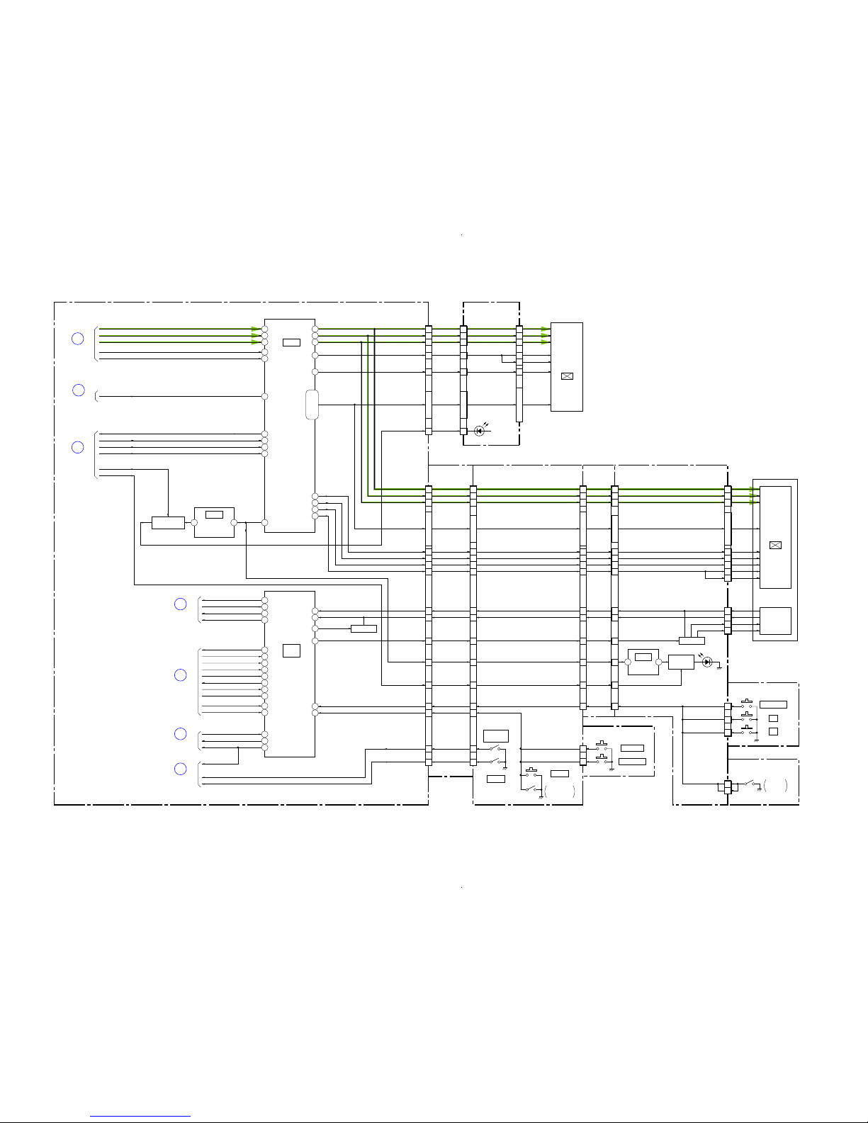
3-3. OVERALL BLOCK DIAGRAM (3/5) ( ) : Number in parenthesis ( ) indicates the division number of schematic diagram where the component is located.
3-5 3-6
A : VIDEO SIGNAL
LCD9002
COLOR
EVF UNIT
SWITCHING
Q6501, 6502
BACKLIGHT
DRIVE
Q6503 - 6506
VC-421 BOARD (3/5)
05
FP-343
FLEXIBLE
BOARD (1/2)
LB-116 BOARD
D302
(BACKLIGHT)
15
14
13
17
7
3 - 6, 8 - 12, 16
5, 9 - 13, 15 - 18
5 - 7, 9, 10, 12 - 15, 20
D6503 - 6505
(BACKLIGHT)
OVERALL (1/5)
(PAGE 3-2)
2
PANEL_R
PANEL_G
PANEL_B
PANEL_XHD
34
33
32
48
1
3
PANEL_XVD
VR
VG
VB
20
21
22
26
10
6 -9, 12, 14,
16, 17, 24, 30
COM_EVF
XSTBY_E
HCK1, HCK2,
HST, PCG,
EN, VCK,VST,
WIDE, VP, REF
EVF_VR
CN5102
EVF_VG
EVF_VB
EVF_COM_CS
EVF_STB
20
31
EXTDA
LED_K
50
COM
45
XSTBY
44
DWN
47
D24
D6
A27
B27
H7
V4
G9
H8
G7
E4
B24
28
18
11
5
COM_PANEL
XSTBY_P
DWN
RGT
RGT
COM
XSTBY
DWN
RGT
EVF_HCK1, EVF_HCK2,
EVF_HST, EVF_PCG,
EVF_EN, EVF_VCK,
EVF_VST, EVF_BLK,
EVF_PSIG, EVF_REF
6
7
8
4
14
3, 4, 6, 9 - 14, 20
3, 4, 6, 9 - 14, 20
32, 38 - 43, 46, 48, 49
17, 23 - 28, 31, 33, 34
6 - 9, 11 - 13, 20 - 22
VR
CN301
VG
VB
COM COM
CS
STB
HCK1, HCK2,
HST, PCG, EN,
VCK, VST, BLK,
PSIG, REF
HCK1, HCK2,
HST, PCG, EN,
VCK, VST,
WIDE, PSIG, REF
HCK1, HCK2, HST,
PCG, EN, VCK,
VST, WIDE, PSIG, REF
COM COM
CS
XSTBY
DWN
RGT
TP_BOT
CN6504
CN6502
CN6503
TP_TOP
TP_L
TP_R
2ND_ZOOM (W)
2ND_S/S_SW
2ND_ZOOM (T)
HCK1, HCK2, HST,
PCG, EN, VCK,
VST, WIDE, PSIG, REF
1
17
18
16
21
11
CN302
19
21
22
23
R
CN5101
(1/2)
CN6404
CN6402
CN6401 (1/2) CN6505CN6506
G
B
R
G
B
R
G
B
CK-154 BOARD (1/2)
FP-377 FLEXIBLE BOARD
FP-346 FLEXIBLE BOARD
CONTROL KEY BLOCK
(SB9000)
2
7
8
5
31
30
29
FP-340
FLEXIBLE
BOARD
35
30
29
32
8
9
10
PD-267 BOARD
2
25
KEY_AD1 KEY_AD1
KEY_AD3_V
KEY_AD3_B
27
7
KEY_AD3
45
2
FRONT_XRESET
50
11
XBATT_VIEW
FRONT_XRESET
XBATT_VIEW
41
12
3
4
25 3
4
5
18
PANEL_BL_ON PANEL_BL_ON
34 5 32
35
TP_SEL1
D5
TP_SEL_2
TP_SEL1
TP_Y
TP_X
17 20 17
37
EXTDA EXTDA
15 22 15
7
8
5
29
28
27
24
14
19
2
23
18
16
192118
16
5
3
PANEL_REVERSE
3
4
6
2
4
5
3
36
TP_X
34
TP_Y
TP_SEL_1
TP_X
TP_Y
43
XCS_EVF
BB_SI
BB_SO
XBB_SCK
XCS_EVF
PANEL_BL_ON
EVF_BL_ON
42
BB_SI
45
BB_SO
44
XBB_SCK
OVERALL (4/5)
(PAGE 3-8)
21
DS/HI CONTROL
(6/7)
IC3001
(2/2)
3 1
BACKLIGHT
CONTROL
IC6501
LCD/EVF DRIVE
(13/14)
IC5101
2.5INCH
COLOR
LCD UNIT
LCD9001
TOUCH PANEL
SWITCHING
Q3004
S3771
PLAY/EDIT
S3773
BACK LIGHT
S003
START/STOP
S002
T
S001
W
S6405
EASY
S6404
PANEL
OPEN/CLOSE
S6403
DISP/
BATT INFO
S6402
RESET
S3461
PANEL
REVERSE
EVF BACKLIGHT
DRIVE
1 3
EVF BACKLIGHT
CONTROL
(13/14)
IC5102
Q5103
XRST_VTR XRST_VTR
OVERALL (4/5)
(PAGE 3-8)
22
OVERALL (1/5)
(PAGE 3-2)
11
OVERALL (1/5)
(PAGE 3-2)
9
HI_SO
HI_SI
XHI_SCK
XCS_IC_2601
CAM_DD_ON
IR_ON
CAM_DD_ON
P4
SYS_V
OVERALL (5/5)
(PAGE 3-9)
24
B26
A12
B25
H11
H9
G11
H10
FRONT_TXD0
FRONT_RXD0
FRONT_SCK0
XFUPSTAT
KEY_AD0
KEY_AD2
FRONT_CS
OVERALL (5/5)
(PAGE 3-9)
23
AC2
XCNM_RESET
D1
XHIDSCON_MAD
N4
OSD_V
 Loading...