

Sony DCJ-500 Service manual
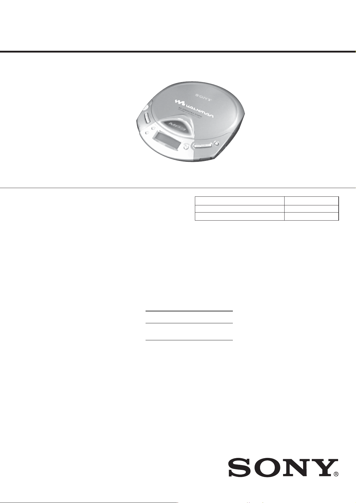
D-CJ500/CJ501/CJ506CK
System
Compact disc digital audio system
Laser diode properties
Material: GaAlAs
Wavelength: λ = 780 nm
Emission duration: Continuous
Laser output: Less than 44.6 µW
(This output is the value measured at a distance
of 200 mm from the objective lens surface on
the optical pick-up block with 7 mm aperture.)
D-A conversion
1-bit quartz time-axis control
Frequency response
20 - 20 000 Hz
+1–3
dB (measured by JEITA CP-
307)
Output (at 4.5 V input level)
CJ500, CJ506CK:
Headphones (stereo minijack)
Approx.5 mW + Approx. 5 mW at 24 Ω
Power requirements
For the area code of the model you
purchased, check the upper left side of the
bar code on the package.
•Two LR6 (size AA) batteries: 3 V DC
•AC power adaptor (DC IN 4.5 V jack):
US/Canadian/E92 model:
120 V, 60 Hz
Battery life* (approx. hours)
(When you use the CD player on a flat and stable
surface.)
Playing time varies depending on how the CD
player is used.
Figures in brackets show the playing time of
MP3 files.
When using G-PROTECTION function
“1” “2”
Two Sony alkaline 32 30
batteries LR6(SG) [24] [24]
(produced in Japan)
*Measured value by the standard of JEITA (Japan
Electronics and Information Technology
Industries Association).
Operating temperature
5°C - 35°C (41°F - 95°F)
Dimensions (w/h/d) (excluding
projecting parts and controls)
Approx. 161.0 × 26.3 × 130.3 mm
(6
3
⁄8 × 1 1⁄16 × 5 1⁄4 in.)
Mass (excluding accessories)
Approx. 210 g (7.5 oz.)
Design and specifications are subject to change
without notice.
Headphones (stereo minijack)
CJ501:
Approx.5 mW + Approx. 5 mW at 16 Ω
(Approx. 1.5 mW + Approx. 1.5 mW
at 16
Ω
)*
*For the customers in France
Supplied accessories
For the area code of the location in which you
purchased the CD player, check the upper left side
of the bar code on the package.
CJ500:
Headphones (1)
AC power adaptor (1)
Headphones/earphones (1)
CJ501:
AC power adaptor (1)
Headphones (1)
Car battery cord (1)
Car connecting pack (1)
Velcro tape (2)
• Abbreviation
E13 : 220-230V AC area in E model.
E92 : Chilean and Peruvian model.
CJ506CK:
AEP/E13/East European/French model:
220 - 230 V, 50/60 Hz
UK model: 230 - 240 V, 50 Hz
Australian model: 240V, 50 Hz
Argentine model: 220 V, 50 Hz
SERVICE MANUAL
Ver 1.1 2002. 05
Photo: D-CJ500
SPECIFICATIONS
US Model
D-CJ500/CJ506CK
Canadian Model
AEP Model
UK Model
E Model
D-CJ501
Australian Model
D-CJ506CK
Model Name Using Similar Mechanism D-EQ550
CD Mechanism Type CDM-3125ER
Optical Pick-up Name DAX-25E
9-873-669-02
2002E1600-1
© 2002.05
Sony Corporation
Personal Audio Company
Published by Sony Engineering Corporation
PORTABLE CD PLAYER

D-CJ500/CJ501/CJ506CK
TABLE OF CONTENTS
1. SERVICING NOTE·························································· 3
2. GENERAL ·········································································· 4
3. DISASSEMBLY ································································ 5
3-1. Battery Case Lid, Cabinet (Upper) Assy ······················· 5
3-2. Upper Lid Assy······························································ 6
3-3. MAIN Board, MD Assy (CDM-3125ER) ····················· 6
3-4. Turn Table Motor Assy (M901)····································· 7
3-5. Motor Assy (Sled) (M902),
Optical Pick-up (DAX-25E)·········································· 7
4. ELECTRICAL ADJUSTMENTS ································· 8
5. DIAGRAMS········································································ 9
5-1. Block Diagram ···························································· 10
5-2. Printed Wiring Board – MAIN Board (Side A) –······· 12
5-3. Printed Wiring Board – MAIN Board (Side B) –······· 13
5-4. Schematic Diagram – MAIN Board (1/4) – ··············· 14
5-5. Schematic Diagram – MAIN Board (2/4) – ··············· 15
5-6. Schematic Diagram – MAIN Board (3/4) – ··············· 16
5-7. Schematic Diagram – MAIN Board (4/4) – ··············· 17
5-8. IC Pin Function Descriptions ······································ 19
6. EXPLODED VIEWS ······················································ 26
6-1. Cabinet (Front) Section ··············································· 26
6-2. Cabinet (Lower) Section ············································· 27
6-3. Optical Pick-up Section (CDM-3125ER)···················· 28
7. ELECTRICAL PARTS LIST······································· 29
This appliance is classified as a CLASS 1 LASER product.
The CLASS 1 LASER PRODUCT MARKING is located on
the rear exterior.
CAUTION
Use of controls or adjustments or performance of procedures
other than those specified herein may result in hazardous
radiation exposure.
Flexible Circuit Board Repairing
•Keep the temperature of the soldering iron around 270 ˚C during repairing.
• Do not touch the soldering iron on the same conductor of the
circuit board (within 3 times).
• Be careful not to apply force on the conductor when soldering
or unsoldering.
Notes on chip component replacement
•Never reuse a disconnected chip component.
• Notice that the minus side of a tantalum capacitor may be damaged by heat.
On AC power adaptor
•Use only the AC power adaptor supplied or
recommended in “Accessories (supplied/
optional).” Do not use any other AC power
adaptor. It may cause a malfunction.
Polarity of the plug
SAFETY-RELATED COMPONENT WARNING!!
COMPONENTS IDENTIFIED BY MARK 0 OR DOTTED LINE WITH
MARK 0 ON THE SCHEMATIC DIAGRAMS AND IN THE PARTS
LIST ARE CRITICAL TO SAFE OPERATION. REPLACE THESE
COMPONENTS WITH SONY PARTS WHOSE PART NUMBERS
APPEAR AS SHOWN IN THIS MANUAL OR IN SUPPLEMENTS
PUBLISHED BY SONY.
2
ATTENTION AU COMPOSANT AYANT RAPPORT
À LA SÉCURITÉ!
LES COMPOSANTS IDENTIFÉS P AR UNE MARQUE 0 SUR LES
DIAGRAMMES SCHÉMA TIQUES ET LA LISTE DES PIÈCES SONT
CRITIQUES POUR LA SÉCURITÉ DE FONCTIONNEMENT. NE
REMPLACER CES COMPOSANTS QUE PAR DES PIÈSES SONY
DONT LES NUMÉROS SONT DONNÉS DANS CE MANUEL OU
DANS LES SUPPÉMENTS PUBLIÉS PAR SONY.
SECTION 1
SERVICING NOTE
D-CJ500/CJ501/CJ506CK
NOTES ON HANDLING THE OPTICAL PICK-UP
BLOCK OR BASE UNIT
The laser diode in the optical pick-up block may suffer electrostatic
breakdown because of the potential difference generated by the
charged electrostatic load, etc. on clothing and the human body.
During repair, pay attention to electrostatic breakdo wn and also use
the procedure in the printed matter which is included in the repair
parts.
The flexible board is easily damaged and should be handled with
care.
NOTES ON LASER DIODE EMISSION CHECK
The laser beam on this model is concentrated so as to be focused on
the disc reflective surface by the objective lens in the optical pickup block. Therefore, when checking the laser diode emission,
observe from more than 30 cm away from the objective lens.
BEFORE REPLACING THE OPTICAL PICK-UP BLOCK
Please be sure to check thoroughly the parameters as par the “Optical
Pick-Up Block Checking Procedures” (Part No.: 9-960-027-11)
issued separately before replacing the optical pick-up block.
Note and specifications required to check are given below.
• FOK output: IC601 yg pin
When checking FOK, remove the lead wire to disc motor.
• RF signal P-to-P value: 0.35 to 0.75 Vp-p
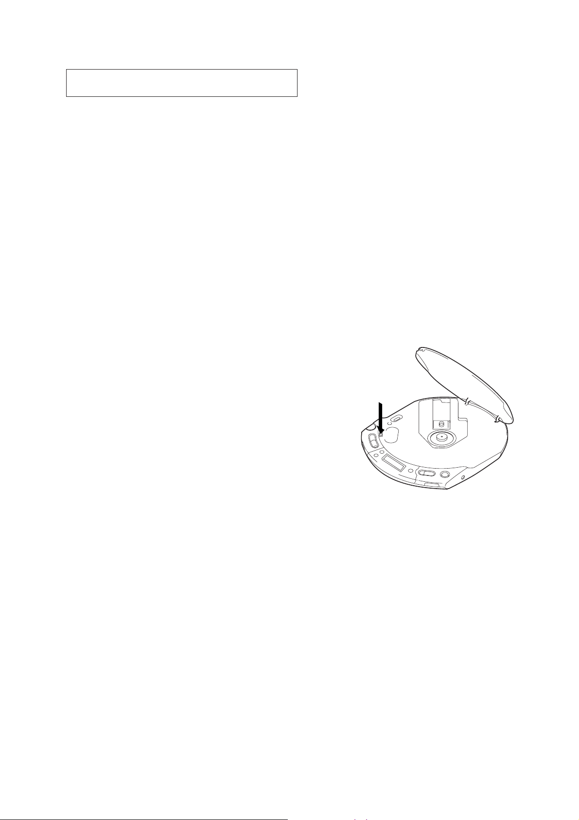
LASER DIODE CHECK
During normal operation of the equipment, emission of the laser
diode is prohibited unless the upper lid is closed while turning ON
the S801. (push switch type)
The following checking method for the laser diode is operable.
• Method:
Emission of the laser diode is visually checked.
1. Open the upper lid.
2. Push the S801 as shown in Fig. 1.
3. Check the object lens for confirming normal emission of the
laser diode. If not emitting, there is a trouble in the automatic
power control circuit or the optical pick-up. During normal
operation, the laser diode is turned ON about 2.5 seconds for
focus searching.
S801
Fig. 1 Method to push the S801
3
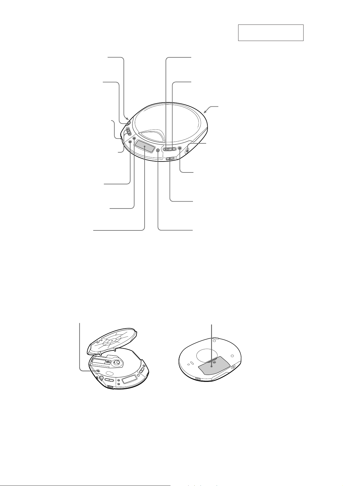
D-CJ500/CJ501/CJ506CK
CD player (front)
SECTION 2
GENERAL
This section is extracted
from instruction manual.
1 i (headphones)
jack
2 OPEN button
3 VOLUME control
4 FOLDER –/+ buttons
5 MENU button
6 DISPLAY button
8 . (AMS/search) button
9 N >* (play, AMS/
search) button
q; Strap holes
qa DC IN 4.5 V
(external power
input) jack
qs x (stop) button
qd HOLD switch
7 Display
*The button has a tactile dot.
CD player (inside)
qg G-PRO (G-PROTECTION) switch
qf SOUND button
CD player (rear)
qh Battery compartment
4
SECTION 3
y
DISASSEMBLY
Note : This set can be disassembled in the order shown below.
SET
BATTERY CASE LID,
CABINET (UPPER) ASSY
(Page 5)
D-CJ500/CJ501/CJ506CK
MAIN BOARD, MD ASSY
(CDM-3125ER)
(Page 6)
MOTOR ASSY (SLED) (M902),
OPTICAL PICK-UP (DAX-25E)
(Page 7)
Note : Follow the disassembly procedure in the numerical order given.
3-1. Battery Case Lid, Cabinet (Upper) Assy
UPPER LID ASSY
(Page 6)
TURN TABLE MOTOR ASSY
(M901)
1
three
(Page 7)
screws (
+B 2 × 10
)
7
four claws
8
four claws
9
0
4
3
battery case lid
two
2
cabinet (upper) ass
5
two claws
boss
6
two claws
screws (
+B 2 × 10
)
5
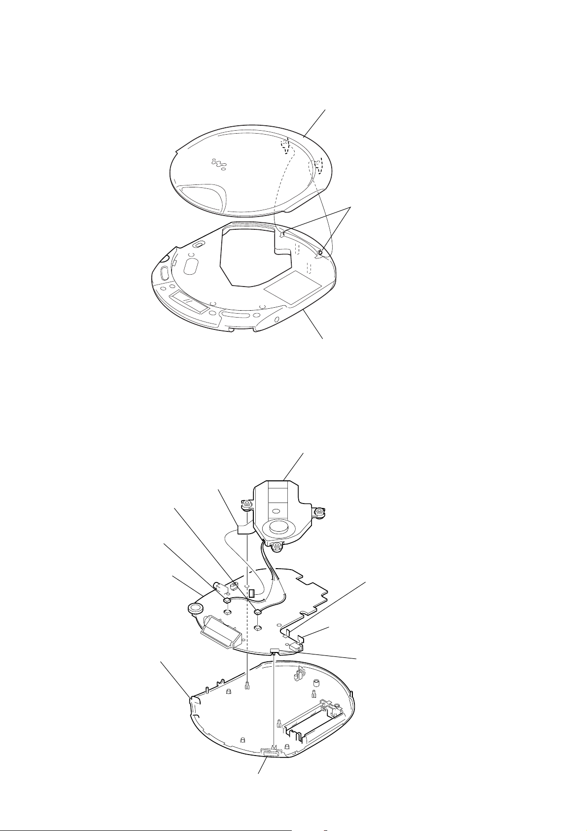
D-CJ500/CJ501/CJ506CK
s
3-2. Upper Lid Assy
2
upper lid assy
1
two claw
3-3. MAIN Board, MD Assy (CDM-3125ER)
Note : When installing, fit S803 to the knob (HOLD).
1
3
2
connector (
5
connector (
CN503)
MAIN Board
connector (
CN502)
CN501)
cabinet (front) assy
4
MD Assy
terminal (–), battery (BT402)
terminal (+.–), battery (BT400)
cabinet (lower) sub assy
knob (HOLD)
S803
6

3-4. Turn Table Motor Assy (M901)
1
three
screws (
+B 1.7 × 5
2
turn table motor assy (spindle) (M901)
chassis
)
D-CJ500/CJ501/CJ506CK
3-5. Motor Assy (Sled) (M902), Optical Pick-up (DAX-25E)
1
feed screw assy
2
6
4
chassis
s
crew (
+B 1.7 × 5
motor assy (sled) (M902)
7
5
3
s
crew (
)
gear B
bracket (Shaft)
optical pick-up
(DAX-25E)
+P 1.4 × 3.5
)
7
D-CJ500/CJ501/CJ506CK
3
SECTION 4
ELECTRICAL ADJUSTMENTS
CD section adjustments are done automatically in this set.
In case of operation check, confirm that focus bias.
FOCUS BIAS CHECK
1. Connect the oscilloscope between TP603 (RF) and GND on
main board.
2. Insert the disc (YEDS-18). (Part No. : 3-702-101-01)
3. Press the B > button.
4. Confirm that the oscilloscope waveform is as shown in the
figure below. (eye pattern)
A good eye pattern means that the diamond shape (
center of the waveform can be clearly distinguished.
• RF signal reference waveform (eye pattern)
VOLT/DIV : 200 mV
TIME/DIV : 500 ns
RF level :
±
0.2 Vp-p
0.55
When observing the eye pattern, set the oscilloscope for AC range
and raise vertical sensitivity.
) in the
◊
Test Point:
– MAIN Board (Side B) –
IC601
04
8
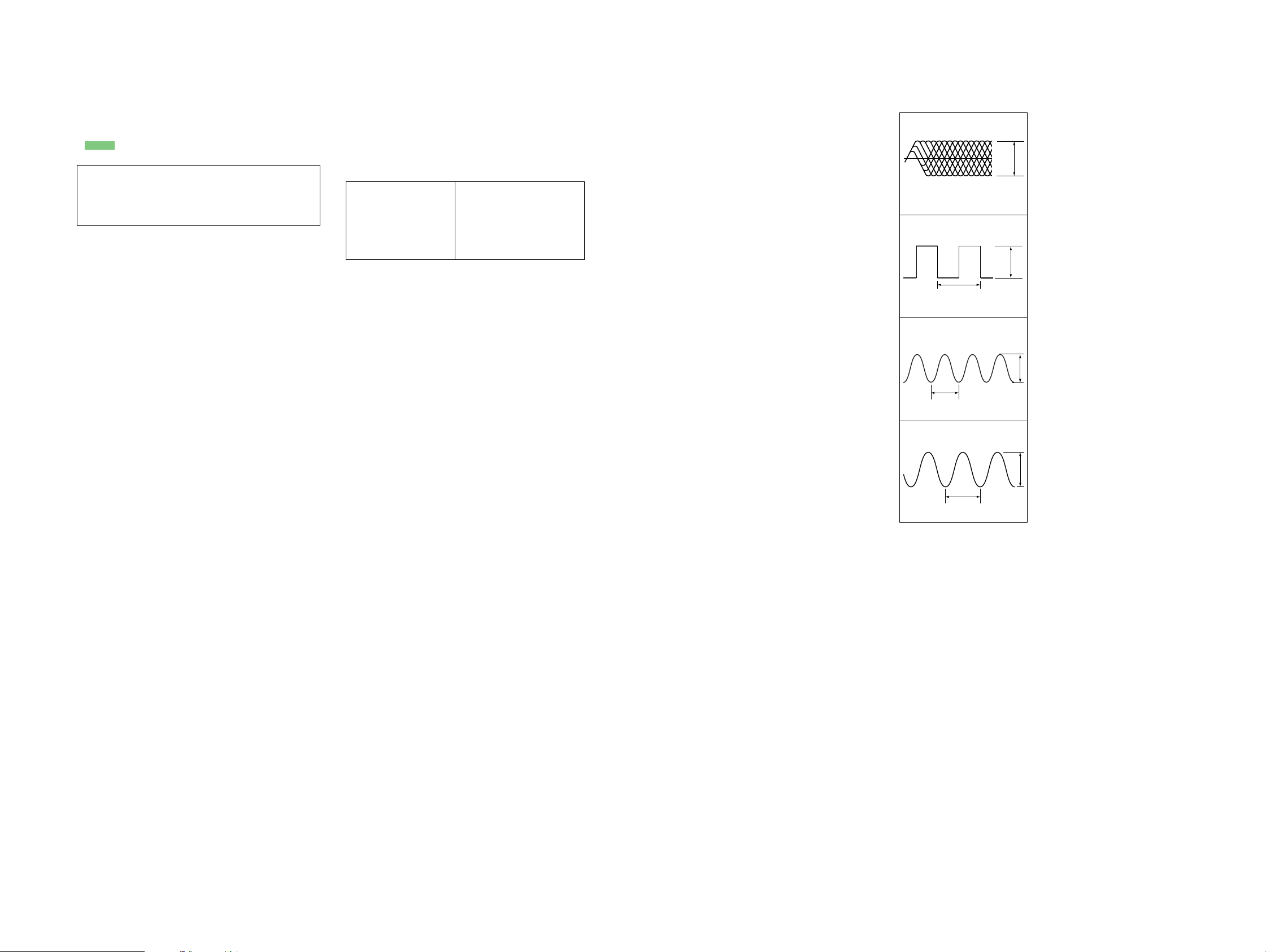
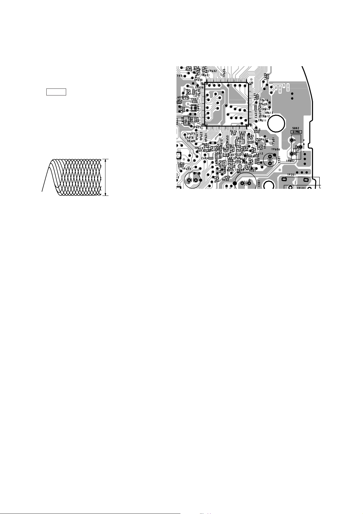
SECTION 5
DIAGRAMS
D-CJ500/CJ501/CJ506CK
Note For Printed Wiring Boards And Schematic Diagrams
Note on Printed Wiring Board
• X : parts extracted from the component side.
• Y : parts extracted from the conductor side.
• : Pattern from the side which enables seeing.
(The other layers' patterns are not indicated.)
Caution:
Pattern face side: Parts on the pattern face side seen from
(Side A) the pattern face are indicated.
Parts face side: Parts on the par ts face side seen from
(Side B) the parts face are indicated.
Note on Schematic Diagram:
• All capacitors are in µF unless otherwise noted. pF: µµF 50 WV or
less are not indicated except for electrolytics and tantalums.
• All resistors are in Ω and 1/
•%: indicates tolerance.
• C : panel designation.
Note:
The components identified by mark 0 or dotted
line with mark 0 are criti-
cal for safety.
Replace only with part
number specified.
• A : B+ Line.
•Total current is measured with CD installed.
•Power voltage is dc 4.5 V and fed with regulated dc power supply
from DC IN jack (J401).
•Voltages and wavef orms are dc with respect to ground in playbac k
mode.
no mark : CD PLAY
•Voltages are taken with a VOM (Input impedance 10 MΩ).
Voltage variations may be noted due to normal production tolerances.
•Waveforms are taken with a oscilloscope.
Voltage variations may be noted due to normal production tolerances.
• Circled numbers refer to waveforms.
• Signal path.
J : CD
c : CD-R/RW (MP3)
•Abbreviation
FR : French model.
4
W or less unless otherwise specified.
Note:
Les composants identifiés par
une marque 0 sont critiques
pour la sécurité.
Ne les remplacer que par une
piéce portant le numéro
spécifié.
• Wavef orms
(CD play mode)
1
TP603 (RF)
600 mVp-p
200 mV/DIV, 400 ns/DIV
2
IC601 <z/n>>(LRCKO)
22.5 µs
500 mV/DIV, 5
3
IC601 rk>(XTAO)
59 ns
500 mV/DIV, 40 ns/DIV
4
IC801 q; (XTALO)
2.5 Vp-p
µ
s/DIV
1.3 Vp-p
3.2 Vp-p
125 ns
1 V/DIV, 40 ns/DIV
99
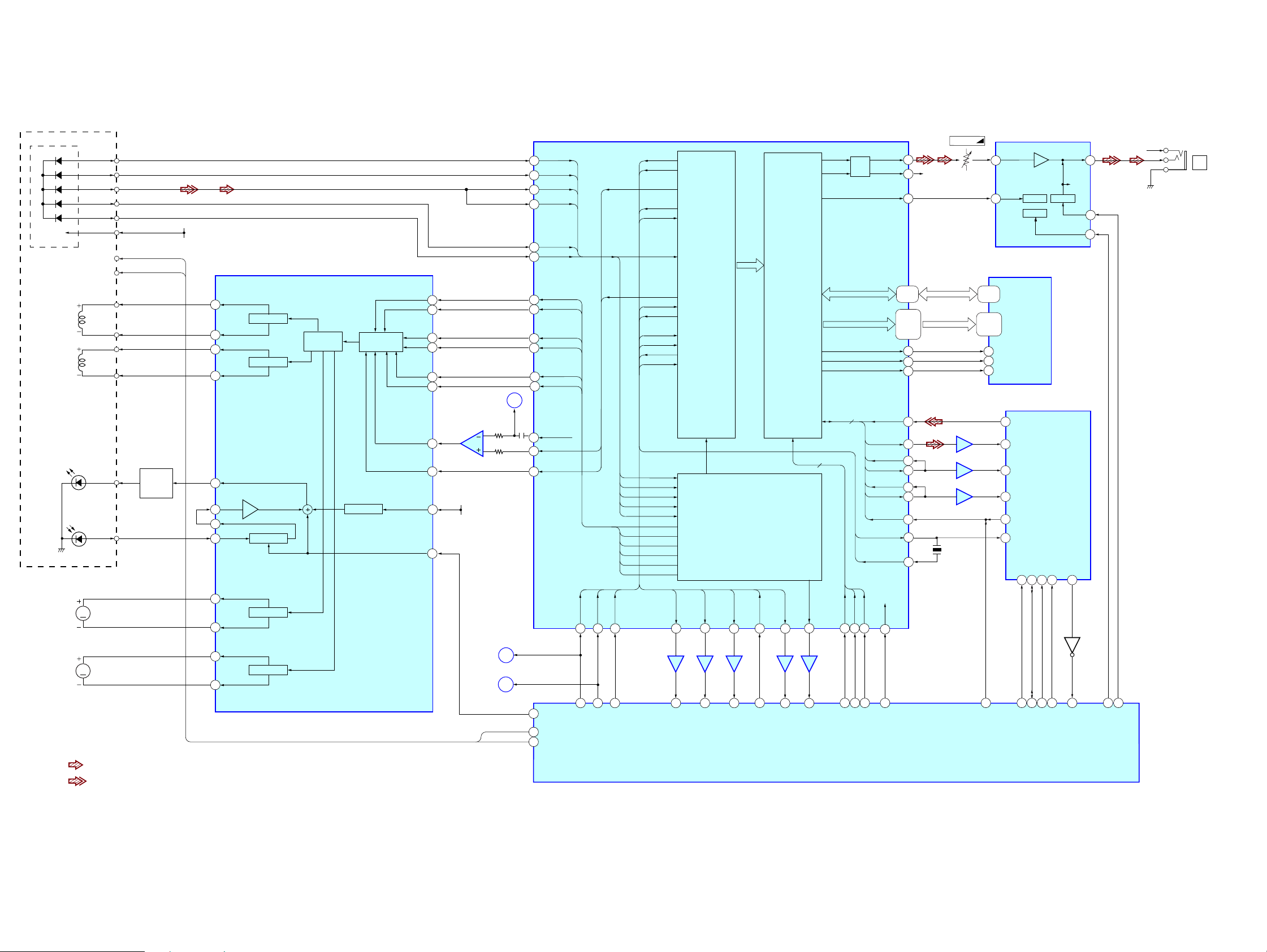
D-CJ500/CJ501/CJ506CK
5-1. Block Diagram – MAIN-1 Section –
DETECTOR
A
B
RF
E
F
VCC
OPTICAL PICK-UP
BLOCK
DAX-25E
FOCUS
COIL
TRACKING
COIL
LD
PD
M902
SLED
MOTOR
M901
SPINDLE
MOTOR
• R-ch is omitted due to
same as L-ch.
• Signal path
:CD
:CD-R/RW(MP3)
A
B
RF
E
F
VCC1 +2V
OPGSW
OPSTB
F+
F–
T+
T–
LD
PD
S+
Q404,405
LD
DRIVER
28
26
23
21
63
64
59
60
32
M
S–
C+
30
19
M
C–
17
FO2
RO2
FO3
RO3
RF2
INM2
RF21
PAPC
FO1
RO1
FO4
RO4
IC401 (1/2)
FOCUS/TRACKING COIL DRIVER,
SPINDLE/SLED MOTOR DRIVER
DRIVER
LEVEL
SHIFTER
DRIVER
PD AMP
DRIVER
DRIVER
CONTROLLER
LD AMP
RI1
RI2
RI3
PWM/FI4
PDL/RI4
VINDET
APCREF
IC601
RF AMP,
DIGITAL SIGNAL PROCESSOR,
DIGITAL SERVO PROCESSOR,
D-RAM CONTROLLER
AOUT1
LPF
A0-A10
7
82
89
XQOK_O
AMUTE_O
D0-D3
XWRE_O
51
AOUT2
56
LRMU
61
4, 3,
6, 5
116-113,
17-15,
13-11,
117
XRAS
1
XWE
2
XCAS
9
PCMD_I
PCMD_O
LRCK_I
107
LRCK_O
BCK_I
111
BCK_O
XRDE
18
XTAO
48
XTAI
47
XRST
28
53 96
XRST_O
IC804
BUFFER
WDCK
GFS
MDS
XTAO
XTAI
RFAC
MDP
XSOE
SENS
XLAT
CLOK
SCOR
SDTO
RFDC
SFDR
SRDR
FFDR
FRDR
TFDR
TRDR
E
F
B
A
SENS
3
5
PROCESSOR
SENS
SIGNAL
BLOCK
SCOR
27
1
7
SCOR_INT
SERVO
BLOCK
WDCK
26
6
2
1740
GRSCOR_INT
CONTROLLER,
XSOE
2422
46
XSOE_O
MEMORY
BUS BOOST
BLOCK
GFS
69
351
87
GFS_I
3
FOK
65
IC803
BUFFER
7
86
FOK_I
SYSTEM CONTROL
SYSM30XQOK31XWRE
25
51
IC801 (1/2)
A
92
B
91
RFDC
88
RFAC
84
E
89
F
90
FI1
33
34
FI2
35
36
FI3
13
14
A
1
3
15
16
62
61
IC403
COMPARATOR
4
B+ +3V
B
C
OPGSW
OPSTB
SYNC
SDTO
SCK
100
99
96
95
98
97
104
103
102
83
100
95
SFDR
SRDR
FFDR
FRDR
TFDR
TRDR
C176
MDP
MDS
STB_RW_O
OPGSW
OPSTB
SDTO
21
41
SDTO
CLOK
XLAT
2320
5542 16
SCK
XLAT
R-CH
X601
16.9MHz
RV301
VOLUME
2, 3,
24, 25
19-12,
15-19,
21,8
5
4
23
IC703
BUFFER
17
35
62
92
14
19
D0-D3
XRAS
XWE
XCAS
12108
14106
13110
60
62
XRDE_O
HEADPHONE AMP
LIN
MUTE
MT SW
PW SW
IC602
D-RAM
A0-A10
SDO
9109
SDI0
LRCKIA
BCKIA
CKO
XI
/RESET
MP3_DSP_RST
IC301
BEEP
PWRSW
IC701
MP3 DECODER
MIDIO
/MICK
STANDBY
19
4554761 98
SCL0(I2C)
SDA0(I2C)
STANDBY_O
LOUT
R-CH
BEEP
PO7
391
Q701
MP3DSP_I
49
44
BEEP_O
XAPCOFF_O
R-CH
8
17
20
J301
i
1010
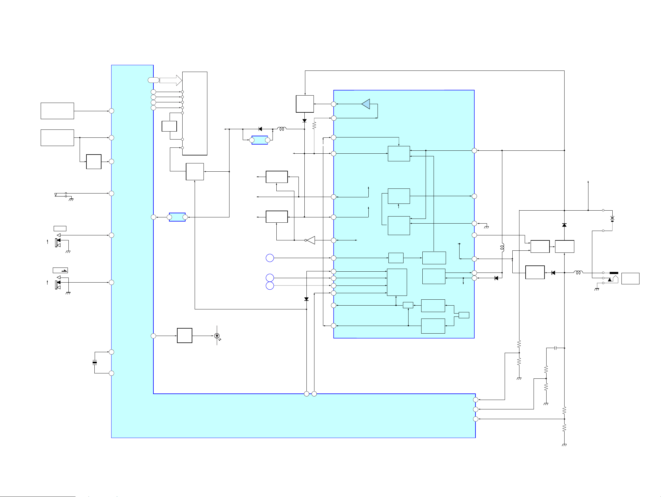
– MAIN-2 Section –
S804 - 807
FUNCTION
KEY
S808 - 811
FUNCTION
KEY
Q801,803
DETECT
S801
(CD DOOR OPEN)
S802
G-PRO
2
1
S803
HOLD
ON
OFF
KEY
28
KEY1_AD
29
KEY2_AD
KEY_INT
19
18
OPENSW_INT
88
GPRO_I
90
HPLD_I
D0 - D7
WR1
LCD_RST_O
XLIGHT-ON
D-CJ500/CJ501/CJ506CK
LCD801
LIQUID CRYSTAL
DISPLAY
56-63
A0
64
RD
77
78
97
Q802
SWITCH
52
IC802
RESETRESET
DD0 - DD7
A0
RD
WR1
LCD_RST_O
V5
V5_OUT
VCPU3V
3115
Q804
LED
DRIVER
Q410
B+
SWITCH
3.0V
D802
DC/DC CONVERTER
VCC1+2V
VCPU +2V
VCC2 _2.5V
D410
IC402
23
Q406
B+ SWITCH
Q407
B+ SWITCH
SYNC
A
SDTO
B
SCK
C
L410
IC701
VDD
D407
D411
Q409
B+
SWITCH
Q408
STNG
54
INP1
48
DTC1D
45
VLGO1
49
VCPU2 (2.0V)
42
VCPU1 (2.5V)
43
VCC1(2.5V)
44
SYNC
5
WAKEUP
6
DATA
8
CLOCK
7
LATCH
9
RSTB
4
VREF
58
VCPU2 (2.0V)
VCPU1 (2.5V)
VCC1
IC401 (2/2)
POWER CONTROL
SWITCHING
POWER
CIRCUIT 2
CHARGE
CONTROL
CHG ON/OFF
CHARGE
SWITCH
CLK
OR OSC
INTERFACE
AMP
SAWTOOTH
GENERATOR
SWITCHING
POWER
CIRCUIT 5
STANDBY
REFERENCE
BANDGAP
REFERENCE
(VREF)
DC IN
VIN
CHGSW
RF4
DCIN
VG
BIAS
53
B+ +3V
HEADPHONE AMP
D403
L401
IC401
IC301
B+
B–
DRY BATTERY
SIZE "AA"
(IEC DESIGNATION LR6)
2PCS,3V
J401
DC IN 4.5V
!
FOCUS/TRACKING COIL DRIVER
SPINDLE/SLED MOTOR DRIVER,
37
RS
38
40
Q403
DC IN
DETECT
Q402
GATE
L405
41
L4
1
VG
2
D408
D404
Q401
SWITCH
X801
8MHz
11
XTALI
10
XTALO
4854
IC801 (2/2)
SYSTEM CONTROL
XPOWLT_O
WAKEUP_O
BAT1MNT_AD
DCINMNT_AD
DCIN_INT
25
21
31
1111
 Loading...