

Sony CXP84724, CXP84720, CXP84716 Datasheet

CXP84716/84720/84724
CMOS 8-bit Single Chip Microcomputer
Description
The CXP84716/84720/84724 is a CMOS 8-bit microcomputer integrating on a single chip an A/D converter,
serial interface, timer/counter, time base timer, capture
timer/counter, FRC capture unit, high-precision timing
pattern generation circuit, PWM output, and the like
besides the basic configurations of 8-bit CPU, ROM,
RAM, and I/O port.
The CXP84716/84720/84724 also provides the
sleep/stop functions that enable to execute the poweron reset function and lower the power consumption.
Features
• A wide instruction set (213 instructions) which covers various types of data.
— 16-bit arithmetic/multiplication and division/Boolean bit operation instructions
• Minimum instruction cycle 250ns at 16MHz operation (4.5 to 5.5V)
333ns at 12MHz operation (3.0 to 5.5V)
• Incorporated ROM capacity 16K bytes (CXP84716)
20K bytes (CXP84720)
24K bytes (CXP84724)
• Incorporated RAM capacity 1120 bytes
• Peripheral functions
— A/D converter 8 bits, 8 channels, successive approximation method
(Conversion time 1.6µs at 16MHz)
— Serial interface Srart-stop synchronization (UART), 1 channel
Incorporated buffer RAM (Auto transfer for 1 to 32 bytes), 2 channels
8-bit clock syncronization (MSB/LSB first selectable), 1 channel
— Timer 8-bit timer, 8-bit timer/counter, 19-bit time base timer,
16-bit capture timer/counter
— FRC capture unit Incorporated 24-bit and 6-stage FIFO
— High-precision timing pattern generation circuit
PPG: maximum of 11 pins, 16 stages programmable, 2 channels
— PWM output 8 bits, 8 channels
• Interruption 19 factors, 15 vectors, multi-interruption possible
• Standby mode Sleep/stop
• Package 100-pin plastic QFP/LQFP
• Piggyback/evaluator CXP84700
100 pin QFP (Plastic) 100 pin LQFP (Plastic)
Structure
Silicon gate CMOS IC
Sony reserves the right to change products and specifications without prior notice. This information does not convey any license by
any implication or otherwise under any patents or other right. Application circuits shown, if any, are typical examples illustrating the
operation of the devices. Sony cannot assume responsibility for any problems arising out of the use of these circuits.
– 1 –
E96Z13-PS

CXP84716/84720/84724
V
SS
V
DD
RST
XTAL
EXTAL
INT4
INT3
INT2
INT1
INT0
NMI
PA0 to PA7
8
PORT A
CLOCK
GENERATOR/
SYSTEM CONTROL
SPC 700
CPU CORE
NMI
PB0 to PB7
8
PORT B
PC0 to PC7
PD0 to PD7
8
PORT C
RAM
1120 BYTES
ROM
16K/20K/24K
8
PORT D
BYTES
PE0 to PE5
PE6 to PE7
PF0 to PF5
PF6
PF7
6
2
PORT E
6
PORT F
INTERRUPT CONTROLLER
PG0 to PG7
8
PORT G
PH0 to PH7
8
PORT H
FIFO
FRC
CAPTURE UNIT
PRESCALER/
TIME BASE TIMER
PI0 to PI7
8
PORT I
RAM
BUFFER
PJ0 to PJ7
8
PORT J
(CH1)
PATTERN
GENERATOR
PROGRAMMABLE
RAM
BUFFER
11 11 4
(CH0)
PATTERN
GENERATOR
PROGRAMMABLE
2
2
EXI3
to
EXI0
PPO21
to
PPO11
PPO10
to
PPO0
AV
REF
AV
REF
AV
SS
Block Diagram
A/D CONVERTER
UART RECEIVER
GENERATOR
UART BAUD RATE
UART TRANSMITTER
8
TxD
RxD
AN0 to AN7
8 BIT PWM GENERATOR 1
8 BIT PWM GENERATOR 2
8 BIT PWM GENERATOR 3
8 BIT PWM GENERATOR 4
8 BIT PWM GENERATOR 5
8 BIT PWM GENERATOR 6
8 BIT PWM GENERATOR 0
PWM0
PWM1
PWM2
PWM3
PWM4
8 BIT PWM GENERATOR 7
PWM5
PWM6
PWM7
– 2 –
RAM
BUFFER
SERIAL
UNIT (CH0)
INTERFACE
SI0
CS0
SO0
SCK0
RAM
BUFFER
SERIAL
UNIT (CH1)
INTERFACE
SI1
CS1
SO1
(CH2)
8 BIT TIMER 1
SERIAL INTERFACE UNIT
SI2
SCK1
8 BIT TIMER/COUNTER 0
EC0
SO2
SCK2
16 BIT CAPTURE
TIMER/COUNTER 2
TO
EC1
CINT

Pin Assignment (Top View) 100-pin QFP package
PG3/PWM3
PG4/PWM4
PG5/PWM5
PG6/PWM6
PG7/PWM7
PF0
PF1
PF2
NC
PG1/PWM1
PG2/PWM2
DD
V
SS
PG0/PWM0
V
PI6/SI2
PI7/SO2
PI4/INT4
PI5/SCK2
PI2/INT2
PI3/INT3
CXP84716/84720/84724
PF3
PF4
PF5
PF6/TxD
PF7/RxD
PD0/PPO0
PD1/PPO1
PD2/PPO2
PD3/PPO3
PD4/PPO4
PD5/PPO5
PD6/PPO6
PD7/PPO7
PC0
PC1
PC2
PC3
PC4
PC5
PC6
PC7
PH0/PPO8
PH1/PPO9
PH2/PPO10
PH3/PPO11
PH4/PPO12
PH5/PPO13
PH6/PPO14
PH7/PPO15
PJ0/PPO16
10
12
13
14
15
16
17
19
25
30
11
18
20
21
22
23
24
26
27
28
29
100
99
98
1
2
3
4
5
6
7
8
9
32
31
33
97
34
96
35
95
36
94
37
93
38
92
39
91
40
90
41
89
42
88
43
44
87
45
86
85
46
84
47
48
83
82
49
81
50
80
78
75
74
73
72
65
62
61
79
77
76
71
70
69
68
67
66
64
63
60
59
58
57
56
55
54
53
52
51
PI1/INT1
PI0/INT0
PE7/TO
PE6
PE5
PE4
PE3/NMI
PE2
PE1/EC1
PE0/EC0
PB7/SO1
PB6/SI1
PB5/SCK1
PB4/CS1
PB3
PB2
PB1
PB0/CINT
SO0
SI0
SCK0
CS0
PA7
PA6
PA5
PA4
PA3/AN7
PA2/AN6
PA1/AN5
PA0/AN4
RST
PJ7/EXI1
PJ6/EXI0
PJ5/PPO21
PJ4/PPO20
PJ3/PPO19
PJ2/PPO18
PJ1/PPO17
Note) 1. NC (Pin 90) is left open.
2. VSS (Pins 41 and 88) are both connected to GND.
XTAL
EXTAL
– 3 –
EXI2
EXI3
SS
AV
REF
AV
DD
AV
AN0
AN1
AN2
AN3
SS
V

Pin Assignment (Top View) 100-pin LQFP package
PG2/PWM2
PG3/PWM3
PG4/PWM4
PG5/PWM5
PG6/PWM6
PG7/PWM7
PF0
PF1
PF2
PF3
PF4
DD
V
NC
PG1/PWM1
SS
PG0/PWM0
V
PI6/SI2
PI7/SO2
PI4/INT4
PI5/SCK2
PI2/INT2
PI3/INT3
CXP84716/84720/84724
PE7/TO
PI0/INT0
PI1/INT1
PF5
PF6/TxD
PF7/RxD
PD0/PPO0
PD1/PPO1
PD2/PPO2
PD3/PPO3
PD4/PPO4
PD5/PPO5
PD6/PPO6
PD7/PPO7
PC0
PC1
PC2
PC3
PC4
PC5
PC6
PC7
PH0/PPO8
PH1/PPO9
PH2/PPO10
PH3/PPO11
PH4/PPO12
PH5/PPO13
10
11
12
13
14
15
16
17
18
19
21
22
25
20
23
24
100
99
98
1
2
3
4
5
6
7
8
9
97
96
95
94
93
92
91
90
89
88
87
86
85
84
83
82
81
80
79
78
77
76
75
74
73
72
71
70
69
68
67
66
65
64
63
62
61
60
59
58
57
56
55
54
53
52
51
PE6
PE5
PE4
PE3/NMI
PE2
PE1/EC1
PE0/EC0
PB7/SO1
PB6/SI1
PB5/SCK1
PB4/CS1
PB3
PB2
PB1
PB0/CINT
SO0
SI0
SCK0
CS0
PA7
PA6
PA5
PA4
PA3/AN7
PA2/AN6
27
26
PH7/PPO15
PH6/PPO14
28
29
PJ1/PPO17
PJ0/PPO16
30
31
PJ3/PPO19
PJ2/PPO18
32
PJ4/PPO20
33
34
PJ6/EXI0
PJ5/PPO21
35
PJ7/EXI1
Note) 1. NC (Pin 88) is left open.
2. VSS (Pins 39 and 86) are both connected to GND.
36
37
RST
38
EXTAL
– 4 –
39
XTAL
40
SS
V
EXI2
41
42
EXI3
43
SS
AV
REF
AV
44
DD
AV
45
46
AN0
47
AN1
48
AN2
49
AN3
50
PA1/AN5
PA0/AN4

Pin Description
CXP84716/84720/84724
Symbol I/O
AN0
to
Input
AN3
PA0/AN4
to
I/O/Input
PA3/AN7
PA4 to PA7
PB0/CINT
PB1 to PB3
PB4/CS1
PB5/SCK1
PB6/SI1
PB7/SO1
I/O
I/O/Input
I/O
I/O/Input
I/O/I/O
I/O/Input
I/O/Output
Analog inputs to A/D converter.
(4 pins)
(Port A)
8-bit I/O port. I/O can be set in
a unit of single bits.
Incorporation of pull-up
resistor can be set through the
software in a unit of 4 bits.
(8 pins)
(Port B)
8-bit I/O port. I/O can be set in
a unit of single bits.
Incorporation of pull-up resistor
can be set through the
software in a unit of 4 bits.
(8 pins)
Description
Analog inputs to A/D converter.
(4 pins)
External capture input to 16-bit
timer/counter.
Chip select input for serial interface
(CH1).
Serial clock I/O (CH1).
Serial data input (CH1).
Serial data output (CH1).
PC0 to PC7
PD0/PPO0
to
PD7/PPO7
PE0/EC0
PE1/EC1
PE2
PE3/NMI
PE4 to PE5
PE6
PE7/TO
I/O
I/O/Real-time
output
Input/Input
Input/Input
Input
Input/Input
Input
Output
Output/Output
(Port C)
8-bit I/O port. I/O can be set in a unit of single bits. Can drive 12mA sink
current. Incorporation of pull-up resistor can be set through the software in
a unit of 4 bits.
(8 pins)
(Port D)
8-bit I/O port. I/O can be set in
a unit of single bits.
Incorporation of pull-up resistor
can be set through the software
in a unit of 4 bits.
Data is gated with PPO contents
PPO0 to PPO7 outputs for programmable
pattern generator (PPG0). Functions as
high-precision real-time pulse output port.
(PPG0: 11 pins; PPG1: 11 pins)
by OR-gate and they are output.
(8 pins)
External event inputs for timer/counter.
(2 pins)
(Port E)
8-bit port. Lower 5 bits are for
input; upper 2 bits are for
Non-maskable interruption request.
output.
(8 pins)
Rectangular wave output for 16-bit
timer/counter.
– 5 –
CXP84716/84720/84724
Symbol I/O
PF0 to PF5
PF6/TxD
PF7/RxD
I/O
Output/Output
Input/Input
PG0/PWM0
to
I/O/Output
PG7/PWM7
PH0/PPO8
to
PH7/PPO15
I/O/Real-time
output
Description
(Port F)
Lower 6 bits are for I/O. I/O can be set in a unit of single bits.
Incorporation of pull-up resistor can be set through the software in a unit
of 4 bits (PF0 to PF3) or 2 bits (PF4,PF5)
PF6 is for output; PF7 is for input.
(8 pins)
UART transmission data output.
UART reception data input.
(Port G)
8-bit I/O port. I/O can be set in
a unit of single bits.
Incorporation of pull-up
resistor can be set through the
PWM outputs.
(8 pins)
software in a unit of 4 bits.
(8 pins)
(Port H)
8-bit I/O port. I/O can be set in
a unit of single bits.
Incorporation of pull-up resistor
can be set through the software
in a unit of 4 bits.
Data is gated with PPO contents
by OR-gate and they are output.
PPO8 to PPO11 (PPG0) outputs and
PPO12 to PPO15 (PPG1) outputs for
programmable pattern generator (PPG0,
PPG1).
Functions as high-precision real-time pulse
output port.
(8 pins)
PI0/INT0
to
PI4/INT4
PI5/SCK2
PI6/SI2
PI7/SO2
PJ0/PPO16
to
PJ5/PPO21
PJ6/EXI0
PJ7/EXI1
EXI2 to EXI3
CS0
SCK0
SI0
I/O/Input
I/O/I/O
I/O/Input
I/O/Output
I/O/Real-time
output
I/O/Input
I/O/Input
Input
Input
I/O
Input
(Port I)
8-bit I/O port. I/O can be set in
External interruption request inputs.
(5 pins)
a unit of single bits.
Incorporation of pull-up resistor
can be set through the software
in a unit of 4 bits.
(8 pins)
Serial clock I/O (CH2).
Serial data input (CH2).
Serial data output (CH2).
(Port I)
8-bit I/O port. I/O can be set in
a unit of single bits.
Incorporation of pull-up resistor
can be set through the software
PPO16 to PPO21 outputs for
programmable pattern generator (PPG1).
Functions as high-precision real-time
pulse output port.
in a unit of 4 bits.
Data is gated with PPO contents
by OR-gate and they are output.
(8 pins)
External inputs to FRC capture unit.
(2 Pins)
External inputs to FRC capture unit.
(2 pins)
Chip select input for serial interface (CH0).
Serial clock I/O (CH0).
Serial data input (CH0).
SO1
I/O/Output
Serial data I/O (CH0).
– 6 –

CXP84716/84720/84724
Symbol
EXTAL
XTAL
RST
NC
AVDD
AVREF
AVSS
VDD
VSS
Input
Output
I/O
Input
I/O
Description
Connects a crystal for system clock oscillation. When a clock is supplied
externally, input it to EXTAL pin and input a reversed phase clock to XTAL
pin.
System reset; active at Low level. This pin is I/O pin, and outputs Low
level at the power on with the power-on reset function is executed. (Mask
option)
Not connected.
Leave this pin open for normal operation.
Positive power supply of A/D converter.
Reference voltage input of A/D converter.
GND of A/D converter.
Positive power supply.
GND.
– 7 –

Data bus
RD (Ports B, I, J)
Ports B, I, J direction
IP
Ports B, I, J data
Pull-up resistor
"0" when reset
"0" when reset
∗
Schmitt input
CINT
CS1
SI1
EXI0
EXI1
∗
Pull-up transistors
approx. 100kΩ (VDD = 4.5 to 5.5V)
approx. 300kΩ (VDD = 3.0 to 3.6V)
I/O Circuit Format for Pins
CXP84716/84720/84724
Pin
PA0/AN4
to
PA3/AN7
4 pins
PA4 to PA7
PB1 to PB3
PF0 to PF5
Port A
Port A
Port B
Port F
Data bus
Pull-up resistor
"0" when reset
Port A data
Port A direction
"0" when reset
RD (Port A)
Port A function
selection
"0" when reset
Pull-up resistor
"0" when reset
Ports A, B, F data
Ports A, B, F direction
"0" when reset
Circuit format
A/D converter
∗
IP
Input
protection
circuit
Input multiplexer
∗
Pull-up transistors
approx. 100kΩ (V
approx. 300kΩ (VDD = 3.0 to 3.6V)
DD = 4.5 to 5.5V)
∗
IP
When reset
Hi-Z
Hi-Z
13 pins
PB0/CINT
PB4/CS1
PB6/SI1
PI6/SI2
PJ6/EXI0
PJ7/EXI1
6 pins
Port B
Port I
Port J
Data bus
RD (Ports A, B, F)
∗
Pull-up transistors
approx. 100kΩ (VDD = 4.5 to 5.5V)
approx. 300kΩ (VDD = 3.0 to 3.6V)
Hi-Z
– 8 –
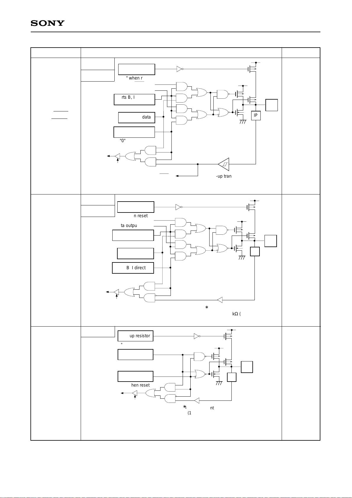
CXP84716/84720/84724
Data bus
RD (Ports B, I)
IP
Ports B, I function
selection
"0" when reset
∗
Schmitt input
SCK in
Ports B, I data
"0" when reset
Pull-up resistor
"0" when reset
SCK OUT
Serial clock output enable
Ports B, I direction
∗
Pull-up transistors
approx. 100kΩ (V
DD = 4.5 to 5.5V)
approx. 300kΩ (VDD = 3.0 to 3.6V)
PB5/SCK1
PI5/SCK2
2 pins
PB7/SO1
PI7/SO2
Port B
Port I
Port B
Port I
"0" when reset
Serial data output enable
Ports B, I function
selection
"0" when reset
Ports B, I direction
"0" when reset
Pull-up resistor
Ports B, I data
SO
Circuit format
When resetPin
Hi-Z
∗
IP
Hi-Z
2 pins
PC0 to PC7
8 pins
Data bus
Port C
RD (Ports B, I)
Pull-up resistor
"0" when reset
Port C direction
"0" when reset
Data bus
Port C data
RD (Port C)
∗
Pull-up transistors
approx. 100kΩ (V
approx. 300kΩ (VDD = 3.0 to 3.6V)
∗
1
Large current
(12mA: VDD = 4.5 to 5.5V)
(5mA: VDD = 3.0 to 3.6V)
∗
2
Pull-up transistors
approx. 100kΩ (VDD = 4.5 to 5.5V)
approx. 300kΩ (VDD = 3.0 to 3.6V)
∗
1
DD = 4.5 to 5.5V)
∗
2
IP
Hi-Z
– 9 –
 Loading...