

Sony CXP84648, CXP84640, CXP84632 Datasheet
CXP84632/84640/84648
CMOS 8-bit Single Chip Microcomputer
Description
The CXP84632/84640/84648 is a CMOS 8-bit single
chip microcomputer integrating on a single chip an
A/D converter, serial interface, timer/counter, time
base timer, capture timer/counter, I2C bus interface,
remote control reception circuit, PWM output, and
32kHz timer/counter besides the basic configurations
of 8-bit CPU, ROM, RAM, and I/O port.
The CXP84632/84640/84648 also provides a sleep/
stop function that enables lower power consumption.
Features
• Wide range instruction system (213 instructions) to cover various of data.
— 16-bit arithmetic/multiplication and division/Boolean bit operation instructions
• Minimum instruction cycle 250ns at 16MHz operation (4.5 to 5.5V)
333ns at 12MHz operation (3.0 to 5.5V)
122µs at 32kHz operation (2.7 to 5.5V)
• Incorporated ROM capacity 32K bytes (CXP84632)
40K bytes (CXP84640)
48K bytes (CXP84648)
• Incorporated RAM capacity 2048 bytes
• Peripheral functions
— A/D converter 8 bits, 8 channels, successive approximation method
(Conversion time 20µs/16MHz)
— Serial interface Srart-stop synchronization (UART), 1 channel
Incorporated buffer RAM (Auto transfer for 1 to 32 bytes), 1 channel
Incorporated 8-bit, 10-stage FIFO
(Auto transfer for 1 to 10 bytes), 1 channel
8-bit clock syncronization (MSB/LSB first selectable), 1 channel
— Timer 8-bit timer, 8-bit timer/counter, 19-bit time base timer,
16-bit capture timer/counter, 32kHz timer/counter
— I2C bus interface
— Remote control reception circuit 8-bit pulse measurement counter, 6-stage FIFO
— PWM output circuit 12 bits, 2 channels
• Interruption 21 factors, 15 vectors, multi-interruption possible
• Standby mode SLEEP/STOP
• Package 80-pin plastic QFP
• Piggyback/evaluation chip CXP84600 80-pin ceramic QFP
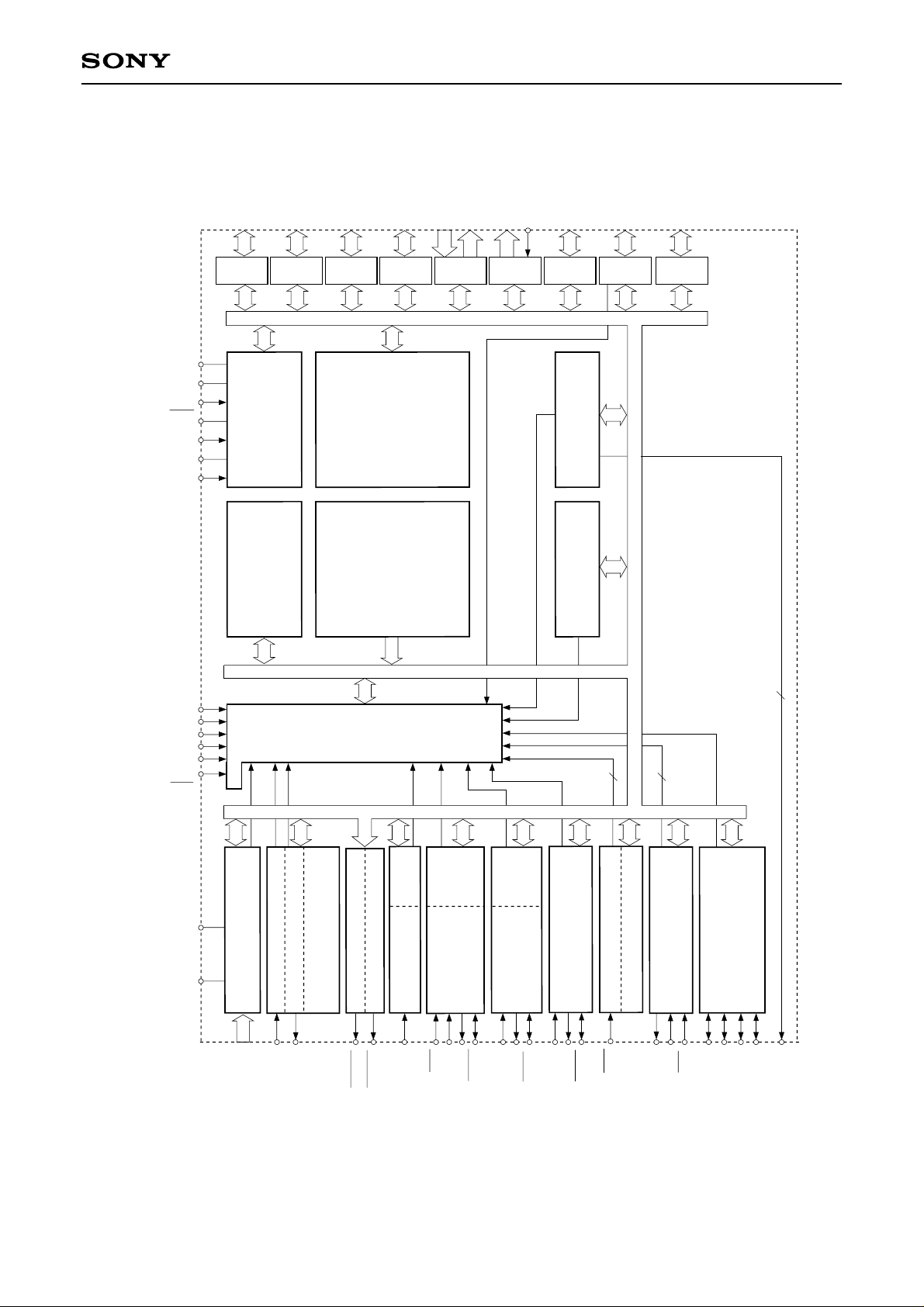
Structure
Silicon gate CMOS IC
80 pin QFP (Plastic)
Perchase of Sony's I2C components conveys a licence under the Philips I2C Patent Rights to use these components
in an I2C system, provided that the system conforms to the I2C Standard Specifications as defined by Philips.
Sony reserves the right to change products and specifications without prior notice. This information does not convey any license by
any implication or otherwise under any patents or other right. Application circuits shown, if any, are typical examples illustrating the
operation of the devices. Sony cannot assume responsibility for any problems arising out of the use of these circuits.
– 1 –
E96309-ST
CXP84632/84640/84648
V
SS
V
DD
RST
XTAL
EXTAL
TX
TEX
PA0 to PA7
8
PB0 to PB7
8
PORT A
CLOCK
GENERATOR/
SYSTEM CONTROL
SPC 700
CPU CORE
PORT B
PC0 to PC7
PD0 to PD7
8
PORT C
RAM
2048 BYTES
ROM
32K/40K/48K BYTES
8
PE0 to PE3
4
PORT D
PE4 to PE5
PF0 to PF6
7
2
PORT E
PF7
PORT F
PG0 to PG7
8
PORT G
PH0 to PH7
8
PORT H
32kHz
TIMER/COUNTER
PRESCALER/
TIME BASE TIMER
PI0 to PI7
8
PORT I
REF
SS
INT4
INT3
INT2
INT1
INT0
NMI
AV
AV
NMI
UART RECEIVER
A/D CONVERTER
UART BAUD RATE
UART TRANSMITTER
8
TxD
RxD
AN0 to AN7
INTERRUPT CONTROLLER
FIFO
BUFFER
GENERATOR
SERIAL
REMOCON IN
12 BIT PWM GENERATOR 1
12 BIT PWM GENERATOR 0
SI0
CS0
RMC
PWM1
PWM0
RAM
SERIAL
UNIT (CH0)
INTERFACE
SI1
SO0
SCK0
FIFO
UNIT (CH1)
INTERFACE
SERIAL INTERFACE UNIT
SI2
SO1
SCK1
SO2
2
2
(CH2)
8 BIT TIMER 1
16 BIT CAPTURE
8 BIT TIMER/COUNTER 0
TO
SCK2
EC0
CINT
C BUS
2
I
TIMER/COUNTER 2
EC1
INTERFACE UNIT
SCL0
SCL1
SDA0
SDA1
2
ADJ
Block Diagram
– 2 –
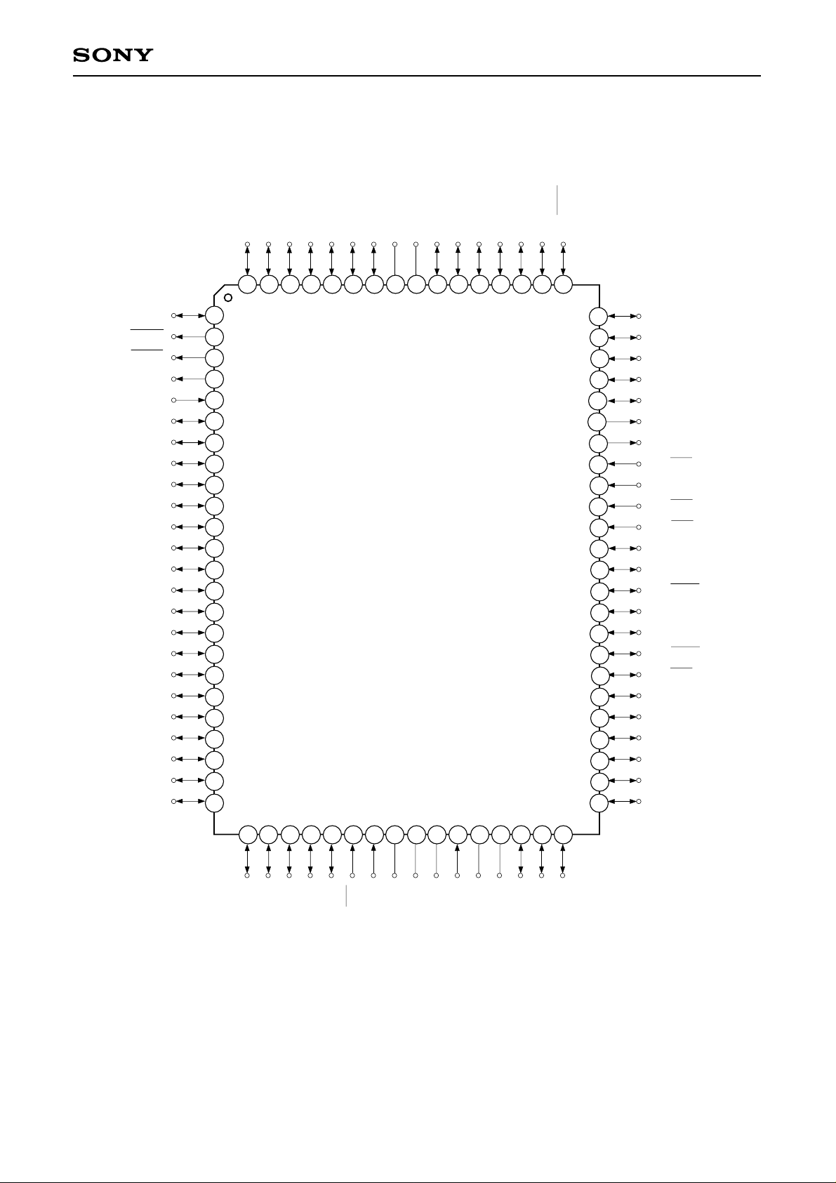
Pin Assignment (Top View)
CXP84632/84640/84648
PF3/SDA0
PF4/PWM0
PF5/PWM1
PF6/TxD
PF7/RxD
PD0
PD1
PD2
PD3
PD4
PD5
PD6
PD7
PC0
PC1
PC2
PC3
PC4
PC5
PC6
PC7
PH0
PH1
PH2
10
11
12
13
14
15
16
17
18
19
20
21
22
23
24
1
2
3
4
5
6
7
8
9
PF1/SCL1
PF2/SDA0
80
79
PF0/SCL0
78
77
PG7
76
PG6
75
PG5
74
PG4
73
NC
72
DD
V
71
PG3
70
PG2
69
PG1
68
PG0
67
PI6/SI2
PI7/SO2
65
66
PI5/SCK2
64
63
62
61
60
59
58
57
56
55
54
53
52
51
50
49
48
47
46
45
44
43
42
41
PI4/INT4
PI3/INT3
PI2/INT2
PI1/INT1
PI0/INT0
PE5/TO/ADJ
PE4
PE3/NMI
PE2/RMC
PE1/EC1
PE0/EC0
PB7/SO1
PB6/SI1
PB5/SCK1
PB4/SO0
PB3/SI0
PB2/SCK0
PB1/CS0
PB0/CINT
PA7/AN7
PA6/AN6
PA5/AN5
PA4/AN4
PA3/AN3
25
PH3
26
PH4
27 28
PH5
PH6
29
PH7
30
RST
31
EXTAL
32
33
XTAL
SS
V
34
TX
35
36
TEX
Note) NC (Pin 73) must be connected VDD.
– 3 –
SS
AV
37
38
REF
AV
40
39
PA1/AN1
PA0/AN0
PA2/AN2
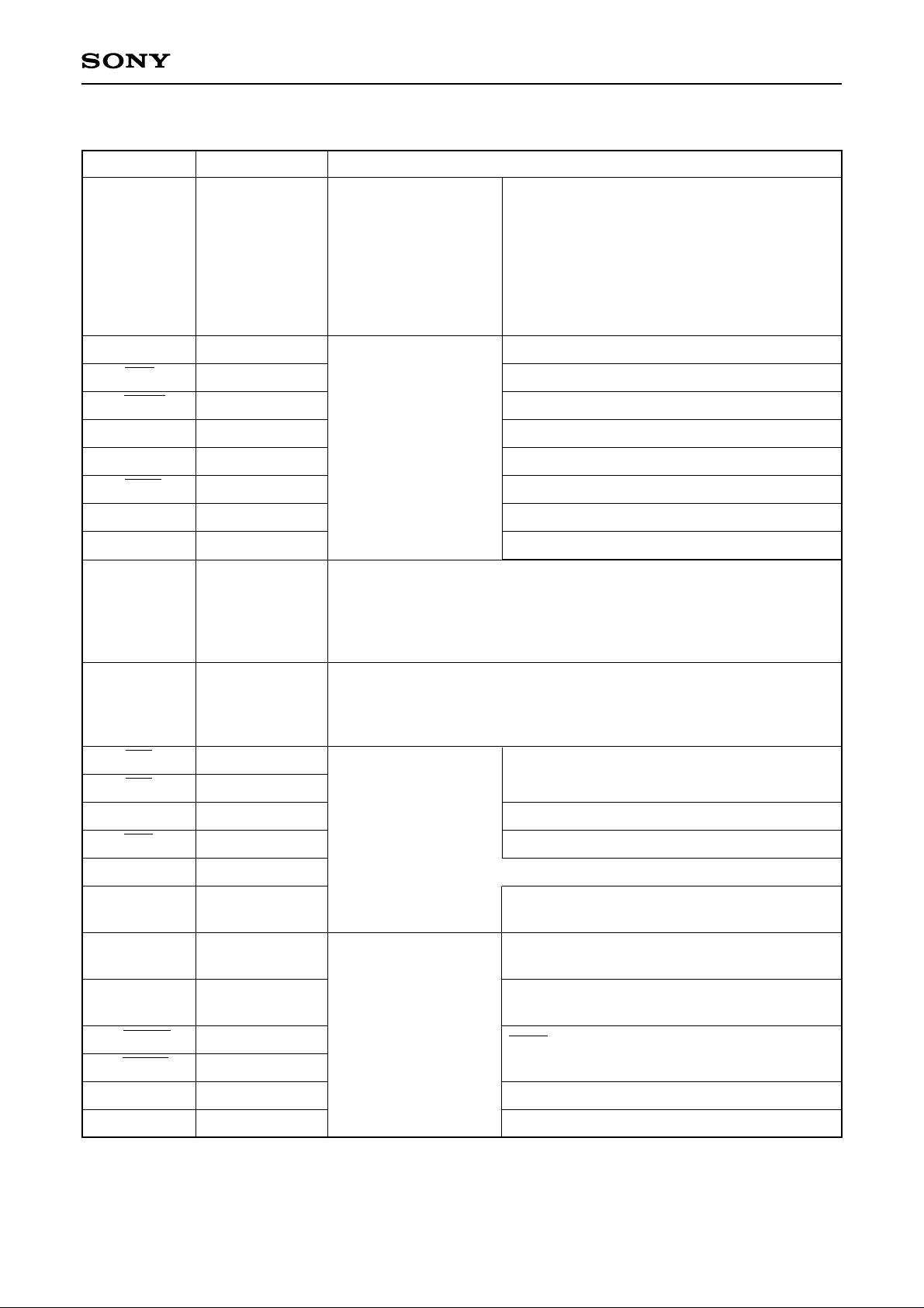
Pin Description
Pin code I/O Functions
(Port A)
8-bit I/O port. I/O can be
PA0/AN0
to
PA7/AN7
I/O/Analog input
set in a unit of signle bits.
Incorporation of the pullup resistance can be set
through the software in a
Analog inputs to A/D converter.
(8 pins)
unit of 4 bits.
(8 pins)
CXP84632/84640/84648
PB0/CINT
PB1/CS0
PB2/SCK0
PB3/SI0
PB4/SO0
PB5/SCK1
PB6/SI1
PB7/SO1
PE0/EC0
PE1/EC1
PE2/RMC
PE3/NMI
PE4
PE5/TO/
ADJ
I/O/Input
I/O/Input
I/O/I/O
I/O/Input
I/O/Output
I/O/I/O
I/O/Input
I/O/Output
I/OPC0 to PC7
I/OPD0 to PD7
Input/Input
Input/Input
Input/Input
Input/Input
Output
Output/Output/
Output
External capture input to 16-bit timer/counter.
(Port B)
I/O can be set in a unit
Chip select input for serial interface (CH0).
Serial clock I/O (CH0).
of single bits for lower
7 bits. Incorporation of
pull-up resistor can be
Serial data input (CH0).
Serial data output (CH0).
set through the software
in a unit of 4 bits.
(8 pins)
Serial clock I/O (CH1).
Serial data input (CH1).
Serial data output (CH1).
(Port C)
8-bit I/O port. I/O can be set in a unit of single bits. Capable of driving
12mA sync current. Incorporation of pull-up resistor can be set through
the software in a unit of 4 bits.
(8 pins)
(Port D)
8-bit I/O port. I/O can be set in a unit of single bits. Incorporation of pullup resistor can be set through the software in a unit of 4 bits.
(8 pins)
External event inputs for timer/counter.
(2 pins)
(Port E)
6-bit port. Lower 4 bits
are for inputs; upper
2 bits are for outputs.
Remote control reception circuit input.
Non-maskable interruption request input.
(6 pins)
Rectangular wave output for 16-bit timer/counter.
Output for 32kHz oscillation frequency division.
PF0/SCL0
PF1/SCL1
PF2/SDA0
PF3/SDA1
PF4/PWM0
PF5/PWM1
PF6/TxD
PF7/RxD
Output/I/O
Output/I/O
Output/Output
Output/Output
Output/Output
Input/Input
(Port F)
Lower 7 bits are for
output; of which lower
4 bits are large current
(12mA) N-ch open
drain output.
The uppermost bit
(PF7) is for input.
(8pins)
– 4 –
Transfer clock I/O for I2C bus interface.
(2pins)
Transfer data I/O for I2C bus interface.
(2pins)
PWM outputs.
(2pins)
UART transmission data output.
UART reception data input.
Pin code I/O Functions
(Port G)
I/OPG0 to PG7
8-bit I/O port. I/O can be set in a unit of single bits. Incorporation of pullup resistor can be set through the software in a unit of 4 bits.
(8 pins)
(Port H)
I/OPH0 to PH7
8-bit I/O port. I/O can be set in a unit of single bits. Incorporation of pullup resistor can be set through the software in a unit of 4 bits.
(8 pins)
PI0/INT0
to
PI4/INT4
I/O/Input
(Port I)
8-bit I/O port. I/O can be
set in a unit of single
External interruption request inputs.
(5 pins)
bits. Incorporation of
PI5/SCK2
PI6/SI2
PI7/SO2
I/O/I/O
I/O/Input
I/O/Output
pull-up resistor can be
set through the software
in a unit of 4 bits.
(8 pins)
Serial clock I/O. (CH2)
Serial data input. (CH2)
Serial data output. (CH2)
CXP84632/84640/84648
EXTAL
XTAL
TEX
RST
NC
AVREF
AVss
VDD
Vss
Input
Crystal connectors for system clock oscillation. When the clock is
supplied externally, input to EXTAL; opposite phase clock should be
Output
Input
OutputTX
Input
input to XTAL.
Crystal connectors for 32kHz timer/counter clock oscillation. For usage
as event counter, input to TEX, and open TX.
Low-level active, system reset.
NC.
Under normal operating conditions, connect to VDD.
Input Reference voltage input for A/D converter.
A/D converter GND.
Positive power supply.
GND.
– 5 –
Data bus
RD (Port B, I)
Port B, I direction
IP
Port B, I data
Pull-up resistance
“0” when reset
“0” when reset
∗
Schmitt input
CINT
CS0
SI0
SI1
∗
Pull-up transistors
approx. 100kΩ
Data bus
RD (Port B, I)
IP
Port B, I function selection
“0” when reset
∗
Schmitt input
SCK in
Port B, I data
Port B, I direction
“0” when reset
Pull-up resistance
“0” when reset
SCK OUT
Serial clock output enable
∗
Pull-up transistors
approx. 100kΩ
I/O Circuit Format for Pins
CXP84632/84640/84648
Pin
PA0/AN0
to
PA7/AN7
8 pins
Port A
Data bus
Port B
Port I
Pull-up resistance
“0” when reset
Port A data
Port A direction
“0” when reset
RD (Port A)
Port A function
selection
AA
“0” when reset
Circuit format
A/D converter
Input multiplexer
∗
approx. 100kΩ
∗
Input protection
IP
circuit
Pull-up transistors
When reset
Hi-Z
PB0/CINT
PB1/CS0
PB3/SI0
PB6/SI1
PI6/SI2
5 pins
PB2/SCK0
PB5/SCK1
PI5/SCK2
3 pins
Port B
Port I
Hi-Z
Hi-Z
– 6 –

CXP84632/84640/84648
Pin
PB4/SO0
PB7/SO1
PI7/SO2
3 pins
Port B
Port I
Data bus
Pull-up resistance
“0” when reset
Serial data output enable
Port B, I function selection
Port B, I direction
RD (Port B, I)
Port C
Pull-up resistance
“0” when reset
“0” when reset
Port B, I data
“0” when reset
Circuit format
SO
∗
Pull-up transistors
approx. 100kΩ
∗
2
When reset
∗
IP
Hi-Z
PC0 to PC7
8 pins
PE0/EC0
PE1/EC1
PE2/RMC
PE3/NMI
PF7/RxD
5 pins
PE4
1 pin
Port E
Port F
Port E
Data bus
Data bus
Port C data
Port C direction
“0” when reset
RD (Port C)
Schmitt input
IP
Port E data
“1” when reset
RD (Port E)
RD (Port E, F)
∗
1
IP
∗
1
Large current 12mA
∗
2
Pull-up transistors
approx. 100kΩ
EC0, EC1, RMC, NMI, RxD
Data bus
Hi-Z
Hi-Z
High level
– 7 –
CXP84632/84640/84648
Pin
PE5/TO/ADJ
1 pin
PD0 to PD7
PG0 to PG7
PH0 to PH7
Port E
Port E data
“1” when reset
Port E function selection (upper)
Port E function selection (lower)
“00” when reset
ADJ16K
ADJ2K
TO
∗
1
∗
1
TO output enable
Port D
Port G
Pull-up resistance
“0” when reset
Port H
Port D, G, H data
Port D, G, H direction
“0” when reset
Circuit format
Internal reset signal
00
01
MPX
10
11
∗
2
∗
1
ADJ signals are frequency dividing output for
32kHz oscillation frequency adjustment.
ADJ2K provides usage as buzzer output.
∗
2
Pull-up transistor approx. 150kΩ
∗
IP
When reset
High level
with approx.
150kΩ
resistor
()
when reset
Hi-Z
24 pins
PI0/INT0
to
PI4/INT4
5 pins
Port I
Data bus
RD (Port D, G, H)
Data bus
Pull-up resistance
“0” when reset
Port I data
Port I direction
“0” when reset
RD (Port I)
INT0
INT1
INT2
INT3
INT4
∗
Pull-up transistors
approx. 100kΩ
∗
IP
∗
Pull-up transistors
approx. 100kΩ
Hi-Z
– 8 –
CXP84632/84640/84648
Pin
PF0/SCL0
PF1/SCL1
PF2/SDA0
PF3/SDA1
4 pins
PF4/PWM0
PF5/PWM1
Port F
I
(“0” when reset)
Port F data
“1” when reset
SCL, SDA
(To I2C circuit)
Port F
SCL, SDA
2
C output enable
PWM
Port F output selection
“0” when reset
Port F data
“1” when reset
Circuit format
Schmitt input
∗
Large current 12mA
When reset
∗
IP
Hi-Z
BUS SW
To internal I2C pin
(SCL1 for SCL0)
High level
2 pins
PF6/TxD
1 pin
PH0 to PH7
Data bus
Port F
UART transmission circuit
Port F output selection
“0” when reset
Port F data
“1” when reset
Data bus
Port H
Data bus
Standby release
RD (Port F)
RD (Port F)
Port H data
“0” when reset
Port H direction
RD (Port H)
High level
IP
Hi-Z
Edge detection
8 pins
Data bus
RD (Port H direction)
– 9 –
 Loading...