

Sony CFDS-03-CP, CFDS-03-CPL Service manual
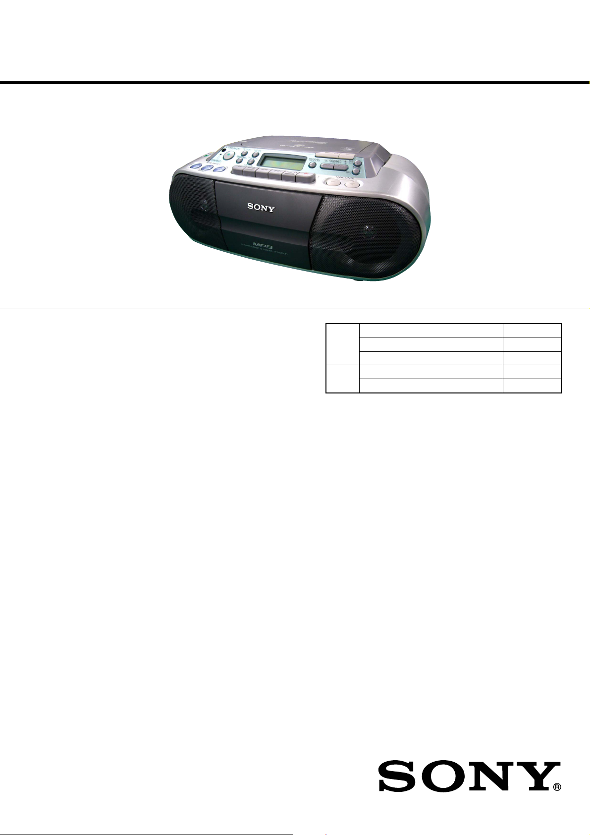
CFD-S03CP/S03CPL
SERVICE MANUAL
Ver. 1.7 2008.03
Photo: CFD-S03CP
CD
Section
TC
Section
Canadian Model
CFD-S03CP
AEP Model
CFD-S03CP/S03CPL
UK Model
E Model
Australian Model
CFD-S03CP
Model Name Using Similar Mechanism CFD-S01
CD Mechanism Type KSM-213CDP
Optical Pick-up Name KSS-213C
Model Name Using Similar Mechanism CFD-S01
Tape Transport Mechanism Type MF-S01
CD player section
System
Compact disc digital audio system
Laser diode properties
Emission duration: Continuous
Laser output: Less than 44.6 µW
(This output is the value measured at a distance of
about 200 mm from the objective lens surface on the
optical pick-up block with 7 mm aperture.)
Number of channels
2
Frequency response
20 - 20 000 Hz +1/–2 dB
Wow and flutter
Below measurable limit
Radio section
Frequency range
FM: 87.5 - 108 MHz
CND, E92, MX model:
AM: 530 - 1 710 kHz
TW model:
AM: 531 - 1 611 kHz
EXCEPT CND, E92, MX, TW model:
AM/MW: 531 - 1 611 kHz (9 kHz step)
530 - 1 610 kHz (10 kHz step)
CFD-S03CPL:
LW: 153 - 279 kHz
IF
FM: 10.7 MHz
AM/MW/LW: 450 kHz
Antennas
FM: Telescopic antenna
AM/MW/LW: Built-in ferrite bar antenna
SPECIFICATIONS
Cassette-corder section
Recording system
4-track 2 channel stereo
Fast winding time
Approx. 150 s (sec.) with Sony cassette C-60
Frequency response
TYPE I (normal): 80 - 10 000 Hz
General
Speaker
Full range: 8 cm dia., 4 Ω, cone type (2)
Outputs
Headphones jack (stereo minijack):
For 16 - 32 Ω impedance headphones
Power output
1.7 W + 1.7 W (at 4 Ω, 10% harmonic distortion)
Power requirements
For CD radio cassette-corder:
120 V AC, 60 Hz (CND, E92, MX, TW model)
220 V AC, 60 Hz (KR model)
220 – 230 V AC, 50 Hz (AR model)
230 V AC, 50 Hz (EXCEPT E92, KR, MX, AR, TW model)
9 V DC, 6 R14 (size C) batteries
For remote control:
3 V DC, 2 R03 (size AAA) batteries
– Continued on next page –
CD RADIO CASSETTE-CORDER
9-887-043-08
2008C04-1
© 2008.03
Sony Corporation
Audio Business Group
Published by Sony Techno Create Corporation

CFD-S03CP/S03CPL
Ver. 1.2
Power consumption
AC 13 W (CND, E92, MX model)
AC 12 W (EXCEPT CND, E92, MX model)
Battery life
For CD radio cassette-corder:
FM recording
Sony R14P: approx. 6 h
Sony alkaline LR14: approx. 20 h
Tape playback
Sony R14P: approx. 3 h
Sony alkaline LR14: approx. 12 h
CD playback
Sony R14P: approx. 1.5 h
Sony alkaline LR14: approx. 4.5 h
Dimensions
Approx. 360 × 141 × 235 mm (w/h/d)
(incl. projecting parts)
Mass
Approx. 2.6 kg (incl. batteries)
Supplied accessory
AC power cord (1)
Remote control (1)
Design and specifications are subject to change
without notice.
•Abbreviation
CND : Canadian model
E92 : AC 120V area in E model
KR : Korea model
MX : Mexican model
AR : Argentina model
TW : Taiwan model
CAUTION
Use of controls or adjustments or performance of procedures
other than those specified herein may result in hazardous
radiation exposure.
Flexible Circuit Board Repairing
• Keep the temperature of the soldering iron around 270˚C during
repairing.
• Do not touch the soldering iron on the same conductor of the
circuit board (within 3 times).
• Be careful not to apply force on the conductor when soldering or
unsoldering.
Notes on Chip Component Replacement
• Never reuse a disconnected chip component.
• Notice that the minus side of a tantalum capacitor may be damaged
by heat.
NOTES ON HANDLING THE OPTICAL PICK-UP BLOCK
OR BASE UNIT
The laser diode in the optical pick-up block may suffer electrostatic
breakdown because of the potential difference generated by the
charged electrostatic load, etc. on clothing and the human body.
During repair, pay attention to electrostatic breakdown and also use
the procedure in the printed matter which is included in the repair
parts.
The flexible board is easily damaged and should be handled with
care.
NOTES ON LASER DIODE EMISSION CHECK
The laser beam on this model is concentrated so as to be focused on
the disc reflective surface by the objective lens in the optical pickup block. Therefore, when checking the laser diode emission,
observe from more than 30 cm away from the objective lens.
SAFETY-RELATED COMPONENT WARNING!!
COMPONENTS IDENTIFIED BY MARK 0 OR DOTTED LINE
WITH MARK 0 ON THE SCHEMATIC DIAGRAMS AND IN
THE PARTS LIST ARE CRITICAL TO SAFE OPERATION.
REPLACE THESE COMPONENTS WITH SONY P ARTS WHOSE
PART NUMBERS APPEAR AS SHOWN IN THIS MANUAL OR
IN SUPPLEMENTS PUBLISHED BY SONY.
Notes on DualDiscs
A DualDisc is a two sided disc product which mates DVD recorded
material on one side with digital audio material on the other side.
However, since the audio material side does not conform to the
Compact Disc (CD) standard, playback on this product is not
guaranteed.
ATTENTION AU COMPOSANT AYANT RAPPORT
À LA SÉCURITÉ!!
LES COMPOSANTS IDENTIFIÉS P AR UNE MARQUE 0 SUR LES
DIAGRAMMES SCHÉMATIQUES ET LA LISTE DES PIÈCES
SONT CRITIQUES POUR LA SÉCURITÉ DE FONCTIONNEMENT.
NE REMPLACER CES COMPOSANTS QUE PAR DES PIÈCES
SONY DONT LES NUMÉROS SONT DONNÉS DANS CE MANUEL
OU DANS LES SUPPLÉMENTS PUBLIÉS PAR SONY.
2

CFD-S03CP/S03CPL
UNLEADED SOLDER
•
Boards requiring use of unleaded solder are printed with the leadfree mark (LF) indicating the solder contains no lead.
(Caution: Some printed circuit boards may not come printed with
the lead free mark due to their particular size.)
: LEAD FREE MARK
Unleaded solder has the following characteristics.
• Unleaded solder melts at a temperature about 40°C higher than
ordinary solder.
Ordinary soldering irons can be used but the iron tip has to be
applied to the solder joint for a slightly longer time.
Soldering irons using a temperature regulator should be set to
about 350°C.
Caution: The printed pattern (copper foil) may peel away if the
heated tip is applied for too long, so be careful!
• Strong viscosity
Unleaded solder is more viscous (sticky, less prone to flow)
than ordinary solder so use caution not to let solder bridges
occur such as on IC pins, etc.
• Usable with ordinary solder
It is best to use only unleaded solder but unleaded solder may
also be added to ordinary solder.
TABLE OF CONTENTS
1. SERVICING NOTES ................................................ 4
2. GENERAL ................................................................... 5
3. DISASSEMBLY
3-1. Cabinet (Rear) Assy......................................................... 7
3-2. Cabinet (Front) Assy, Cabinet (Upper) Assy ................... 7
3-3. Main Board ...................................................................... 8
3-4. CD Block Assy ................................................................ 8
3-5. BD83S Board .................................................................. 9
3-6. Optical Pick-up ................................................................ 9
3-7. Panel Board ..................................................................... 10
3-8. CD Lid ............................................................................. 10
3-9. Tape Mechanism Block, Belt (1), Belt (2) ...................... 11
3-10. TC Board ......................................................................... 11
3-11. Key-1 Board, Key-2 Board .............................................. 12
3-12. Power Board .................................................................... 12
4. MECHANICAL ADJUSTMENTS......................... 13
5. ELECTRICAL ADJUSTMENTS
Tape Section .................................................................... 13
Tuner Section................................................................... 14
CD Section ...................................................................... 16
6. DIAGRAMS
6-1. Block Diagram – CD Section – ....................................... 17
6-2. Block Diagram – Main Section – .................................... 18
6-3. Circuit Boards Location .................................................. 19
6-4. Printed Wiring Board – BD83S Section – ....................... 20
6-5. Schematic Diagram – BD83S Section – .......................... 21
6-6. Printed Wiring Board – Main Section – .......................... 22
6-7. Schematic Diagram – Main Section (1/3) – .................... 23
6-8. Schematic Diagram – Main Section (2/3) – .................... 24
6-9. Schematic Diagram – Main Section (3/3) – .................... 25
6-10. Printed Wiring Boards – TC Section – ............................ 26
6-11. Schematic Diagram – TC Section – ................................ 27
6-12. Printed Wiring Boards – Panel Section – ........................ 28
6-13. Schematic Diagram – Panel Section – ............................ 29
6-14. Printed Wiring Boards – Power Supply Section – ........... 30
6-15. Schematic Diagram – Power Supply Section – ............... 31
7. EXPLODED VIEWS
7-1. Rear Cabinet Section ....................................................... 39
7-2. Front Cabinet Section (1) ................................................ 40
7-3. Front Cabinet Section (2) ................................................ 41
7-4. Upper Cabinet Section (1) ............................................... 42
7-5. Upper Cabinet Section (2) ............................................... 43
7-6. CD Mechanism Section ................................................... 44
8. ELECTRICAL PARTS LIST .................................. 45
3
CFD-S03CP/S03CPL
Ver. 1.4
SECTION 1
SERVICING NOTES
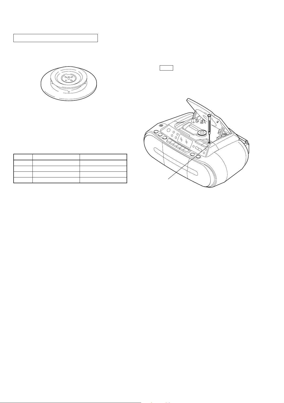
CHUCK PLATE JIG ON REPAIRING
On repairing CD section, playing a disc without the lid (CD), use
Chuck Plate Jig.
• Code number of Chuck Plate Jig: X-4918-255-1
NOTE FOR REPLACEMENT OF THE IC804 AND
IC806
There have been changes to the 3.3V regulator circuit in the course
of production.
When repairing the 3.3V regulator circuit, check which of TYPE A
or B is applicable as specified in the table below.
Ref. No. TYPE A TYPE B
IC804 S-816A33AMC-BAI-T2-G NO MOUNT
IC806 NO MOUNT XC6202P332FR
R883 100k NO MOUNT
R884 220k NO MOUNT
LASER DIODE AND FOCUS SEARCH OPERATION
CHECK
1. Turn ON the [OPERATE] button and press [CD] button to CD
position.
2. Open the CD lid.
3. Turn on SW2 with screwdriver, etc. as following figure.
4. Press the N X (CD) button.
5. Confirm the laser diode emission while observing the objecting
lens. When there is no emission, Auto Power Control circuit or
Optical Pick-up is broken.
Objective lens moves up and down three times for focus search.
SW2
4
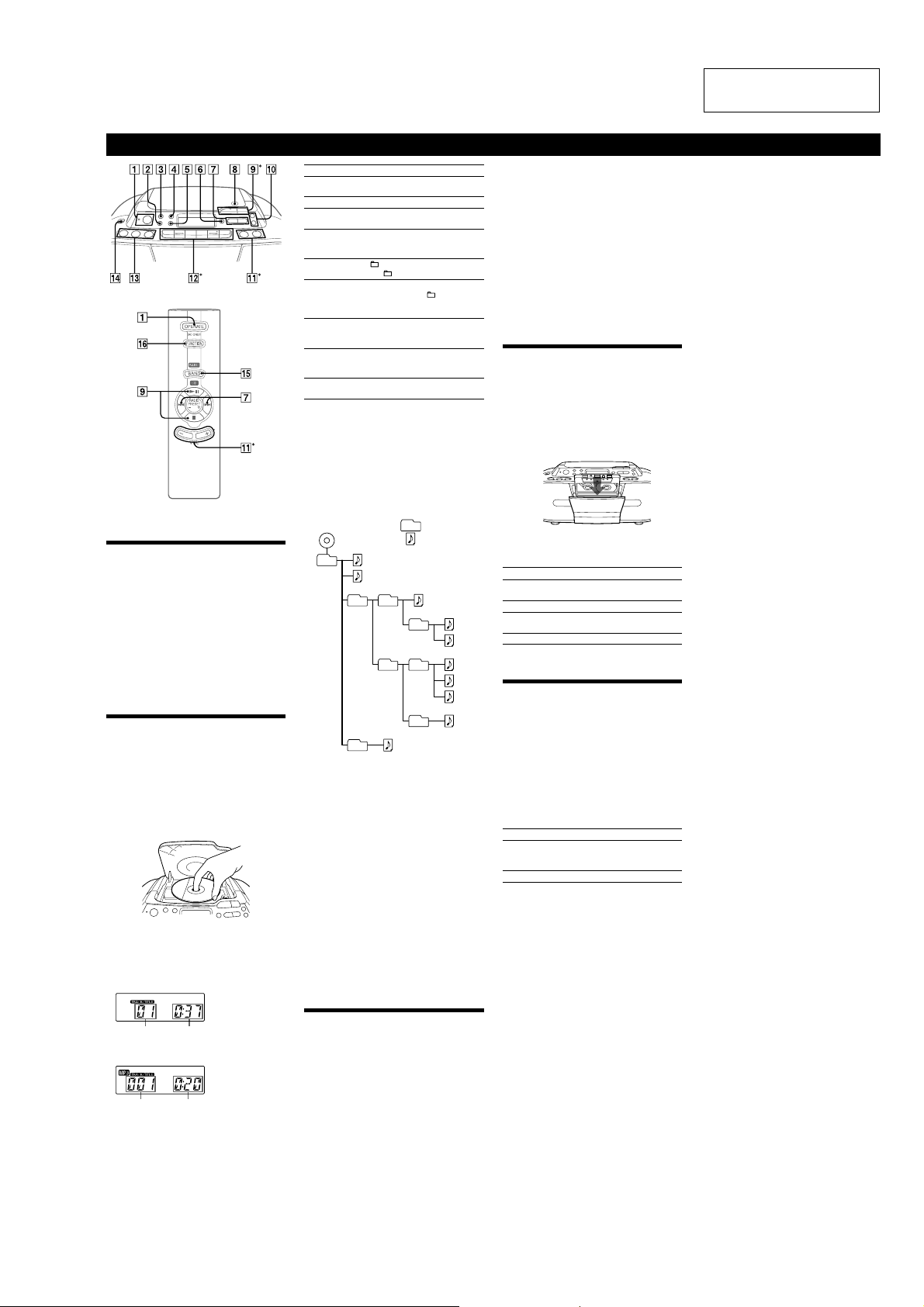
Basic Operations
*
qa
, u 9 and n qs on the
Before using the unit
To turn on/off the power
European model: Press OPERATE 1.
Other models: Press POWER
1
.
To adjust the volume
Press VOLUME +, – (VOL +, – on the remote) qa.
To listen through headphones
Connect the headphones to the i (headphones) jack qf.
To reinforce the bass sound
Press MEGA BASS 2.
“MEGA BASS” appears in the display.
To return to normal sound, press the button again.
Playing a CD/MP3 disc
1
Press CD qd on the unit (direct power-on).
(On the remote, press OPERATE or POWER and
1
then press FUNCTION qh repeatedly until “CD”
appears in the display.)
2
Press Z PUSH OPEN/CLOSE 8 on the unit,
and place a disc with the label side up on the CD
compartment.
To close the CD compartment, press Z PUSH OPEN/
CLOSE
8
on the unit.
3
Press u 9.
The player plays all the tracks/MP3 files once.
When you play a MP3 disc, MP3 indicator lights up
after the player reads the file information.
Audio CD
Track
number
Playing
time
MP3 disc
MP3 file
number
After the folder name*, song title
and artist name are displayed,
the playing time** will appear.
*
**
To Press
Pause playbacku 9. To resume play, press it
again.
Stop playback
x
9.
Go to the next
track/MP3 file
>
7.
Go back to the
previous track/
MP3 file
.
7.
Select a folder on
an MP3 disc
+ 0 on the unit to go forward
and
– 0 to go backward.
Play the selected
folder only (MP3
disc only)
MODE
4
on the unit until
“FLDR” appears,
+ or – 0 on
the unit to select a folder and then
u
9 to start playing.
Locate a point
while listening to
the sound
>
(forward) or . (backward)
7
while playing and hold it until
you find the point.
Locate a point
while observing
the display
>
(forward) or . (backward)
7
in pause and hold it until you
find the point.
Remove the CD
Z
PUSH OPEN/CLOSE 8 on the
unit.
Tips
•
•
x
9
in stop mode. When you open
Example of folder structure and playing
order
The playing order of the folders and files is as follows:
CD-R
CD-RW
3
2
1
2
4
5
3
6
7
8
4
9
5
0
6
1
Folder
MP3 file
Notes on MP3 discs
•
•
•
•
•
•
•
•
•
Listening to the radio
1
Press RADIO•BAND•AUTO PRESET qd on the
unit (BAND
qg
on the remote) repeatedly (direct
power-on).
Each time you press the button, the indication changes
as follows:
CFD-S03CPL: “FM” t “MW” t “LW”
CFD-S03CP: “FM” t “AM”
2
Hold down TUNE + or – 0 until the frequency
digits begin to change in the display.
The player automatically scans the radio frequencies
and stops when it finds a clear station.
If you can not tune in a station, press TUNE + or –
0
repeatedly to change the frequency step by step.
When an FM stereo broadcast is received, “ST”
appears.
Tip
If the FM broadcast is noisy, press MODE until “MONO” appears
4
in the display and the radio will play in monaural.
Changing the AM/MW tuning interval
If you need to change the AM/MW tuning interval, do
the following:
1
Press RADIO•BAND•AUTO PRESET qd on the
unit until “AM” or “MW” is displayed.
2
Press DISPLAY•ENTER 5 on the unit for 2
seconds.
3
Press RADIO•BAND•AUTO PRESET qd on the
unit for 2 seconds.
“9K STEP” or “10K STEP” flashes.
4
Press PRESET + or – 7 on the unit to select
“9K STEP” for 9 kHz interval or “10K STEP” for
10 kHz interval.
5
Press DISPLAY•ENTER 5 on the unit.
After changing the tuning interval, you need to reset your
preset AM/MW radio stations.
Playing a tape
Use buttons on the unit for the operation.
1
Press TAPE qd on the unit (direct power-on).
2
Press xZ qs on the unit, and insert the tape into
the tape compartment with the side you want to
play facing you. Use TYPE I (normal) tape only.
Close the compartment.
Make sure there is no slack in the tape to avoid
damaging the tape or the unit.
3
Press n qs.
The player starts playing.
To Pr ess
Pause playbackX qs on the unit. To resume play,
press it again.
Stop playback
xZ
qs on the unit.
Fast-forward or
rewind*
m
or M (fast forward or
rewind)
qs
on the unit.
Eject the cassette
xZ
qs on the unit.
*
xZ
qs to release m or
qs
.
Recording on a tape
Use buttons on the unit for the operation.
1
Press xZ qs on the unit to open the tape
compartment and insert a blank tape with the
side you want to record on facing you. Use TYPE
I (normal) tape only. Close the compar tment.
2
Select the program source you want to record.
To record from the CD player, insert a CD and press
CD
qd
.
To record from the radio, tune in the station you want.
3
Press z qs on the unit to start recording
(
n
is depressed automatically).
To Press
Pause recording
X
qs on the unit.
To resume recording, press it
again.
Stop recording
xZ
qs on the unit.
Tips
•
•
z
qs in step 3, press MODE 4 on the unit to select the
•
•
1
2
qd
on the unit.
3
z
qs
on the unit.
When the disc is inserted, the player reads all the files on that disc.
During this time, “READING” is displayed. If there are many
folders or non-MP3 files on the disc, it may take a long time for play
to begin or for the next MP3 file to start play.
We recommend that you do not save unnecessary folders or files
other than MP3 ones in the disc to be used for MP3 listening.
A folder that does not include an MP3 file is skipped.
Maximum number of files: 255
Maximum number of folders: 150 (including the root folder)
Maximum number of folders and files in total: 256
Maximum directory levels: 8
Folder names and file names can be displayed with up to 30
characters including quotation marks.
The characters A - Z, 0 - 9, and _ can be displayed on this player.
Other characters are displayed as “_”.
This player conforms to Version 1.0, 1.1, 2.2, 2.3 and 2.4 of the
ID3 tag format. When the file has the ID3 tag information, “song
title”, “artist name” and “album name” can be displayed and
“ID3” appears in the display. If the file does not have the ID3 tag
information, file name appears instead of song title, folder name
appears instead of album name and “no artist” appears instead of
artist name. The ID3 tag information can be displayed with up to 15
characters.
When naming, be sure to add the file extension “mp3” to the file
name.
If you put the extension “mp3” to a file other than an MP3 file, the
player cannot recognize the file properly and will generate random
noise that could damage your speakers.
The file name does not correspond to the ID3 tag.
Adjusting the volume or the audio emphasis will not affect the
recording level.
If the AM/MW/LW program makes a whistling sound after you’ve
press
position of ISS (Interference Suppress Switch) that most decreases
the noise.
For the best results, use the AC power as a power source for
recording.
To erase a recording, proceed as follows:
Insert the tape whose recording you want to erase.
Press TAPE
Press
When the tape is wound to the end, press
M
Playback starts from the track/MP3 file you last stopped playing
(Resume play). During stop, the track/MP3 file number to be played
is displayed.
To cancel the resume play (to start play from the beginning of the
first track/MP3 file), press
the CD compartment or turn off the unit, the resume play is also
canceled.
If there is no folder, “ROOT” appears in the display.
If the playing time is more than 100 minutes, it appears “--:--” in
the display.
VOLUME + (VOL + on the remote)
unit have a tactile dot.
SECTION 2
GENERAL
CFD-S03CP/S03CPL
This section is extracted
from instruction manual.
5
CFD-S03CP/S03CPL
SECTION 3
DISASSEMBLY
Note: This set can be disassemble according to the following sequence.
SET
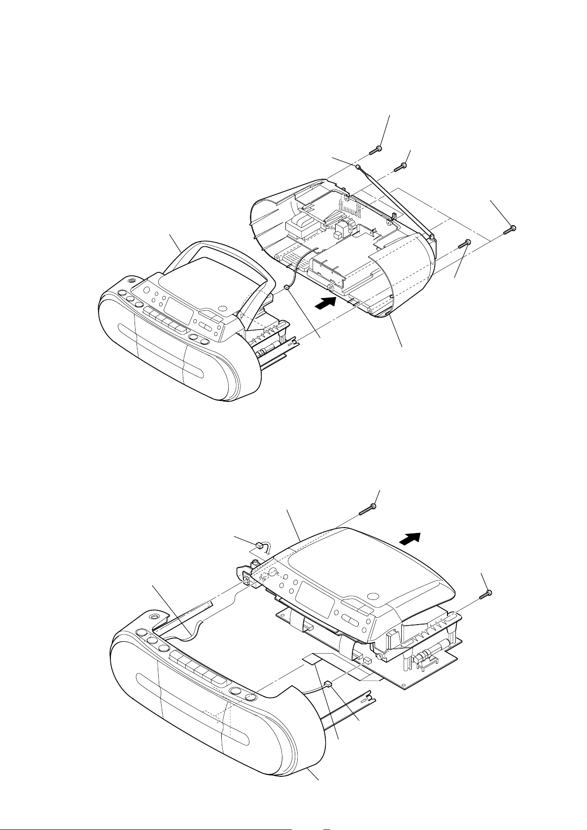
3-1. CABINET (REAR) ASSY
(Page 7)
3-2. CABINET (FRONT) ASSY,
CABINET (UPPER) ASSY
(Page 7)
3-3. MAIN BOARD
(Page 8)
3-4. CD BLOCK ASSY
(Page 8)
3-9. TAPE MECHANISM BLOCK,
3-12. POWER BOARD
BELT (1), BELT (2)
(Page 11)
3-7. PANEL BOARD
(Page 10)
(Page 12)
3-11. KEY-1 BOARD,
KEY-2 BOARD
(Page 12)
3-10. TC BOARD
(Page 11)
3-8. CD LID
(Page 10)
3-5. BD83S BOARD
(Page 9)
3-6. OPTICAL PICK-UP
(Page 9)
6
Note: Follow the disassembly procedure in the numerical order given.
)
3-1. CABINET (REAR) ASSY
telescopic antenna
handle
5
CFD-S03CP/S03CPL
2
screw
(+BV tapping B2.6)
1
two
screws
(+BV tapping (B2.6))
4
three
(+BV tapping (B2.6))
3
(+BV tapping B2.6)
screws
screw
6
3-2. CABINET (FRONT) ASSY, CABINET (UPPER) ASSY
9
cabinet (upper) assy
1
CN308 (4P)
5
flexible flat cable (4 core)
(CN403)
CN305 (3P)
7
cabinet (rear) assy
2
screw
(+BV tapping B2.6)
4
3
(+BV tapping B2.6
screw
6
CN304 (4P)
7
flexible flat cable (14 core)
(CN301)
8
cabinet (front) assy
7
CFD-S03CP/S03CPL
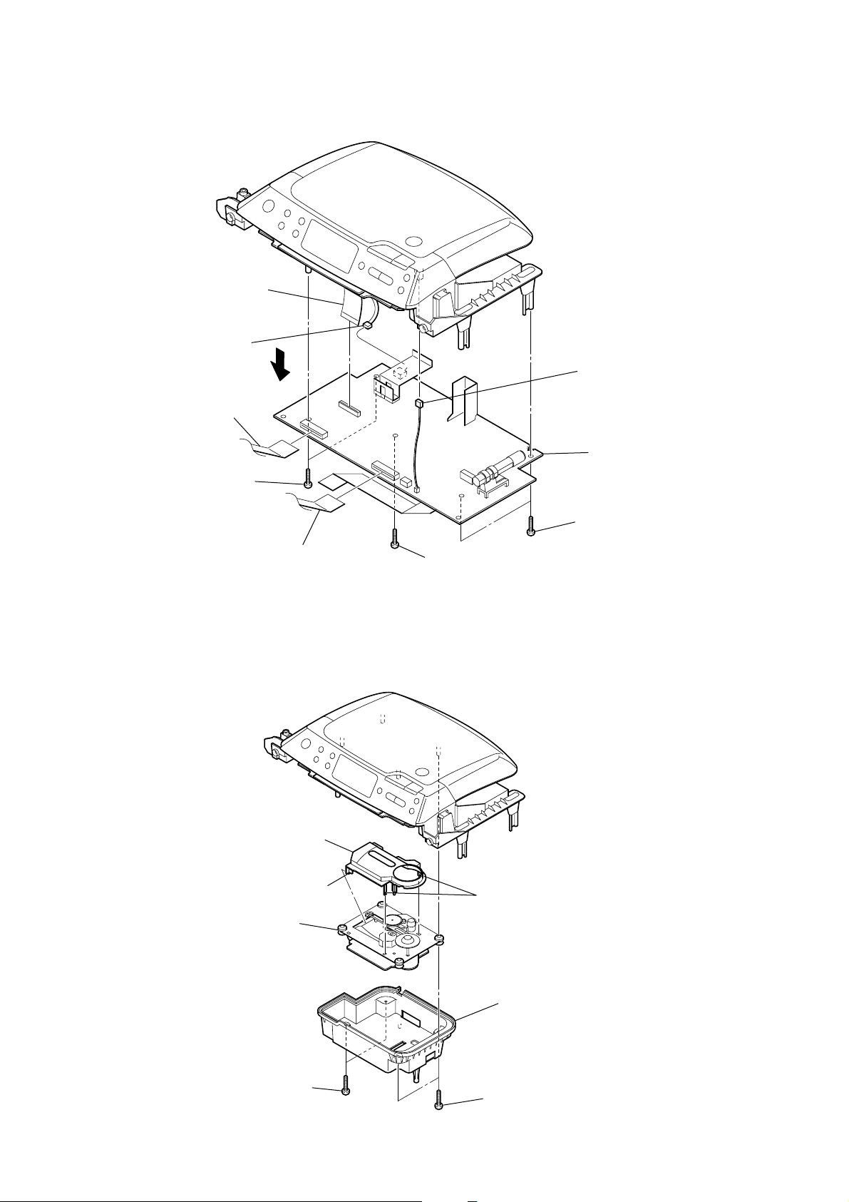
3-3. MAIN BOARD
9
flexible flat cable(23 core)
(CN805)
1
CN306 (4P)
3
flexible flat cable(20 core)
(CN803)
8
4
connector
(S801)
7
two
screws
(+BV tapping B2.6)
3-4. CD BLOCK ASSY
2
flexible flat cable(20 core)
(CN804)
4
CD cover
6
screw
(+BV tapping B2.6)
0
MAIN board
5
two
screws
(+BV tapping B2.6)
5
CD block assy
2
two
screws
(+BV tapping (B2.6))
claw
two claws
3
CD chassis
1
two
screws
(+BV tapping (B2.6))
8
3-5. BD83S BOARD
t
1
flexible flat cable(16 core)
(CN301)
4
Remove the two solders.
5
BD83S board
3
Remove the two solders.
CFD-S03CP/S03CPL
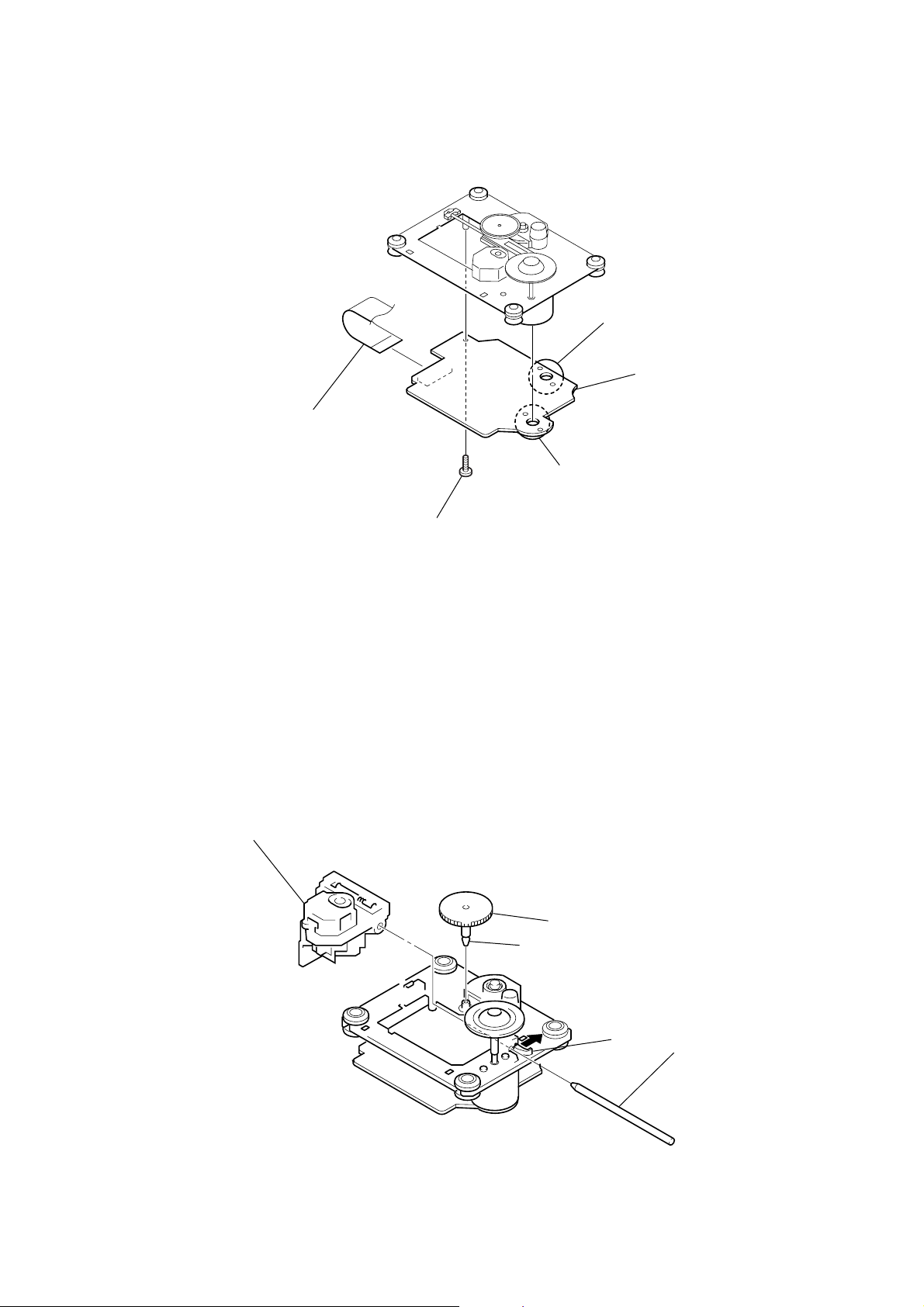
3-6. OPTICAL PICK-UP
5
optical pick-up
2
screw
(+BVTT 2
×
6)
claw
1
gear (A)
3
2
claw
sled shaf
4
9
CFD-S03CP/S03CPL
d
g
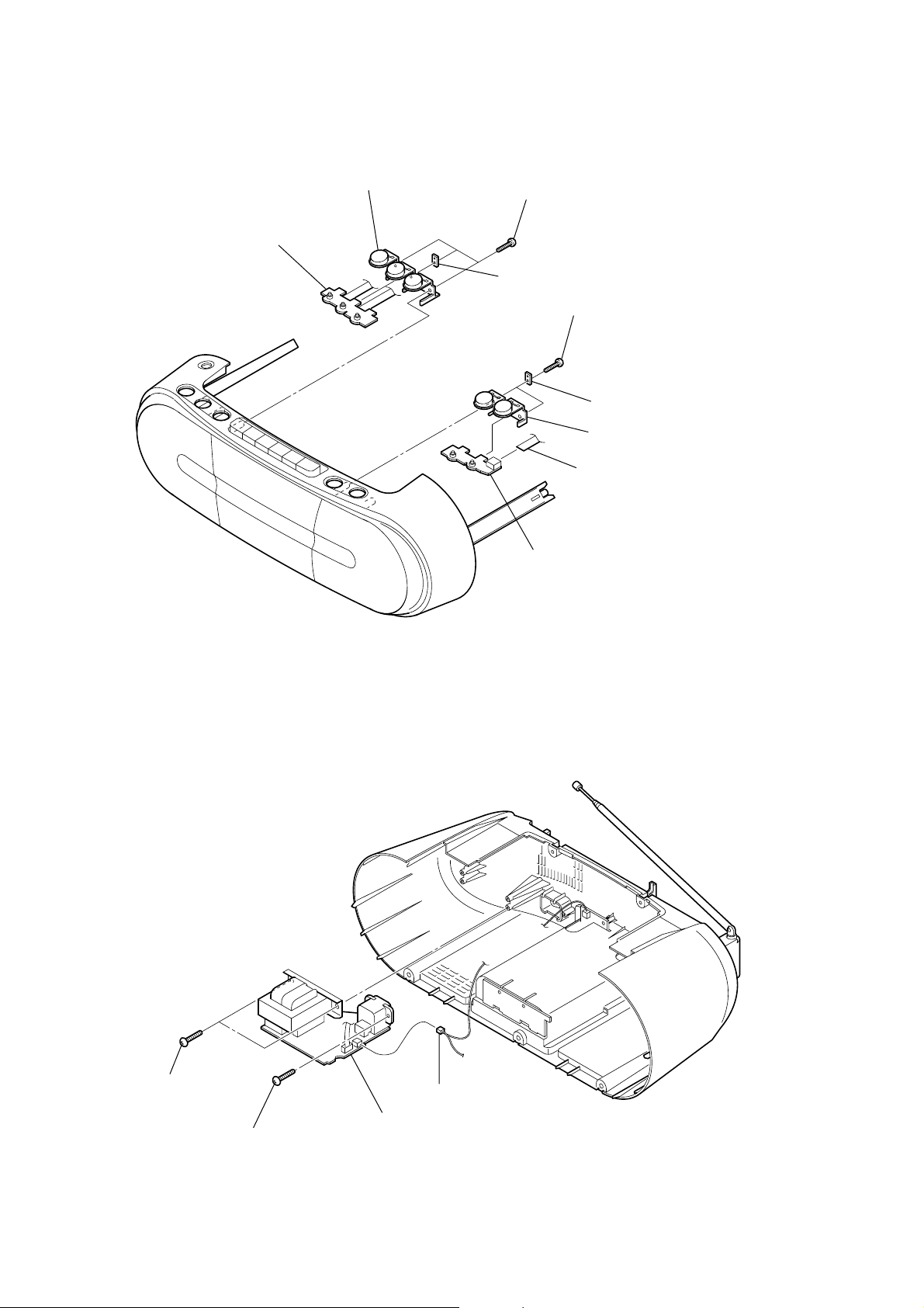
3-7. PANEL BOARD
3
PANEL boar
3-8. CD LID
2
five
screws
(+P tapping (B2.6))
5
CD lid
1
1
four
(+P tapping (B2.6))
2
screws
4
3
6
CD sprin
10
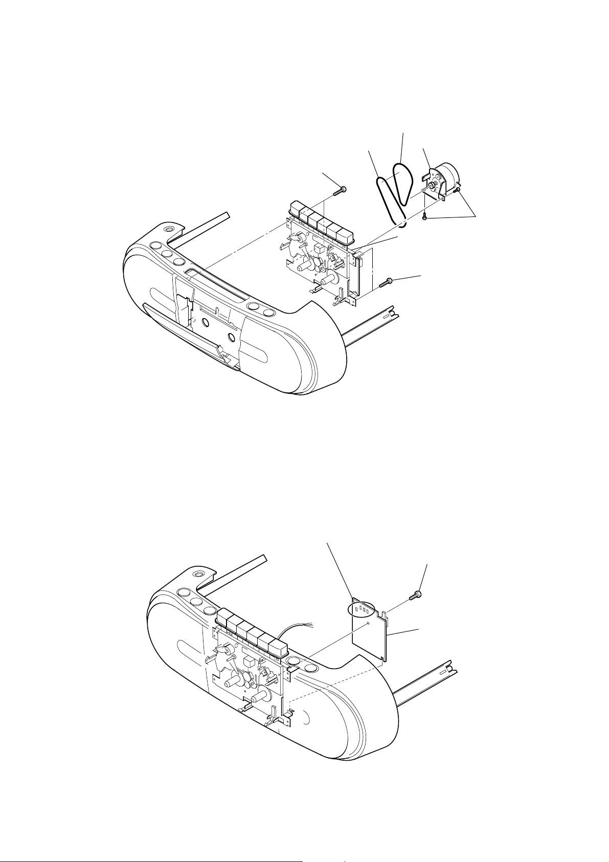
3-9. TAPE MECHANISM BLOCK, BELT (1), BELT (2)
1
two
screws
(+BV tapping (B2.6))
7
belt (2)
CFD-S03CP/S03CPL
6
belt (1)
5
motor bracket
3
tape mechanism block
2
two
screws
(+BV tapping (B2.6))
4
two screws
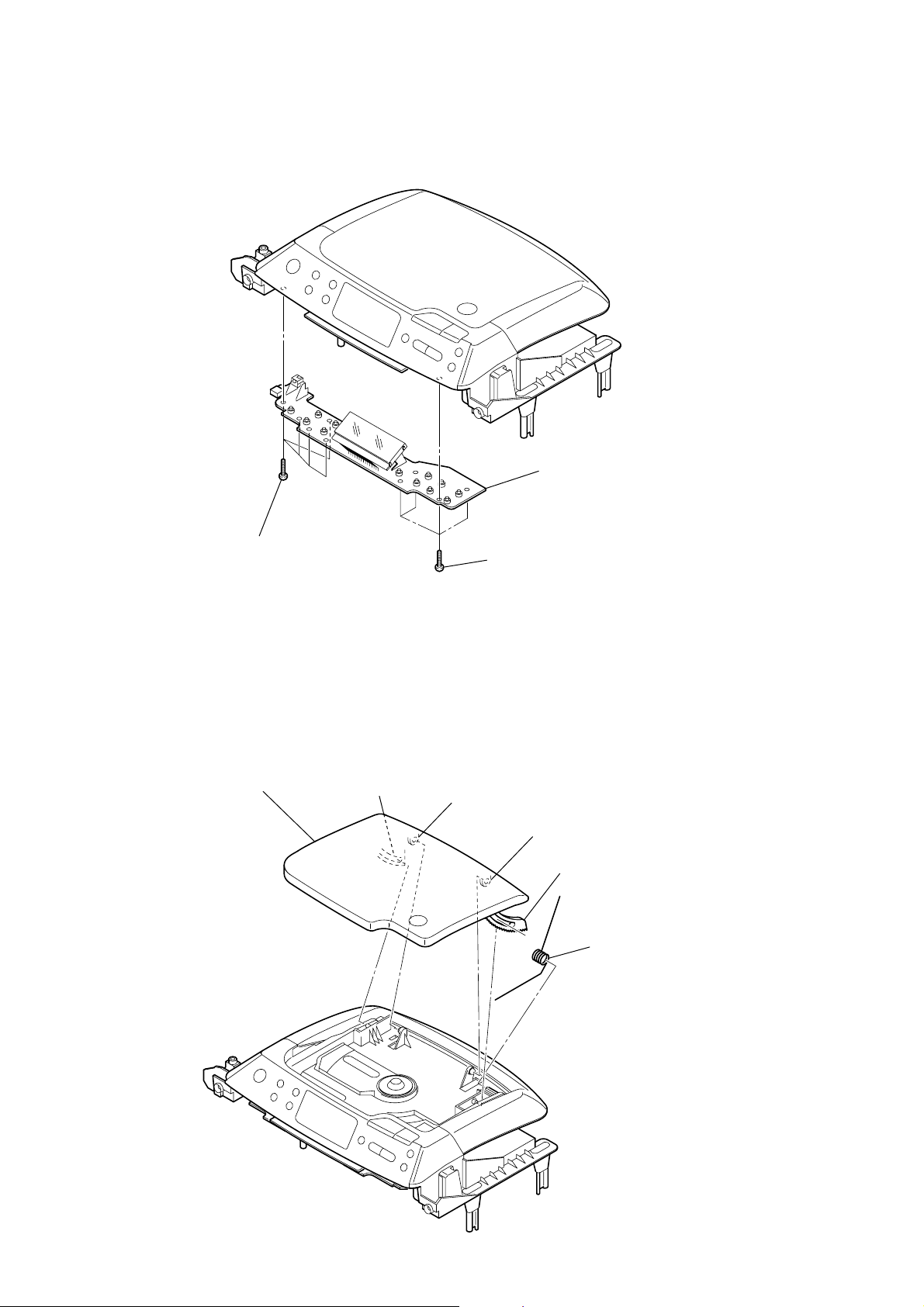
3-10. TC BOARD
2
Remove the four solders.
1
screw
(+P tapping (B2.6))
3
TC board
11
CFD-S03CP/S03CPL
3-11. KEY-1 BOARD, KEY-2 BOARD
8
KEY-1 board
9
button (FUNC)
6
three
(+BV tapping (B2.6))
7
HOLDER board
screws
2
two
(+BV tapping (B2.6))
3
5
1
flexible flat cable(4 core)
(CN421)
screws
two HOLDER boards
button (volume)
3-12. POWER BOARD
4
KEY-2 board
12
3
two
screws
(+BV tapping (B2.6))
2
screw
(+BV tapping (B2.6))
1
4
POWER board
CN902 (2P)
SECTION 4
MECHANICAL ADJUSTMENTS
CFD-S03CP/S03CPL
SECTION 5
ELECTRICAL ADJUSTMENTS
PRECAUTION
1. Clean the following parts with a denatured-alcohol-moistened
swab :
record/playback head pinch roller
erase head rubber belts
capstan idlers
2. Demagnetize the record/playback head with a head demagnetizer.
(Do not bring the head magnetizer close to the erase head.)
3. Do not use a magnetized screwdriver for the adjustments.
4. The adjustments should be performed with the rated power
supply voltage (9V) unless otherwise noted.
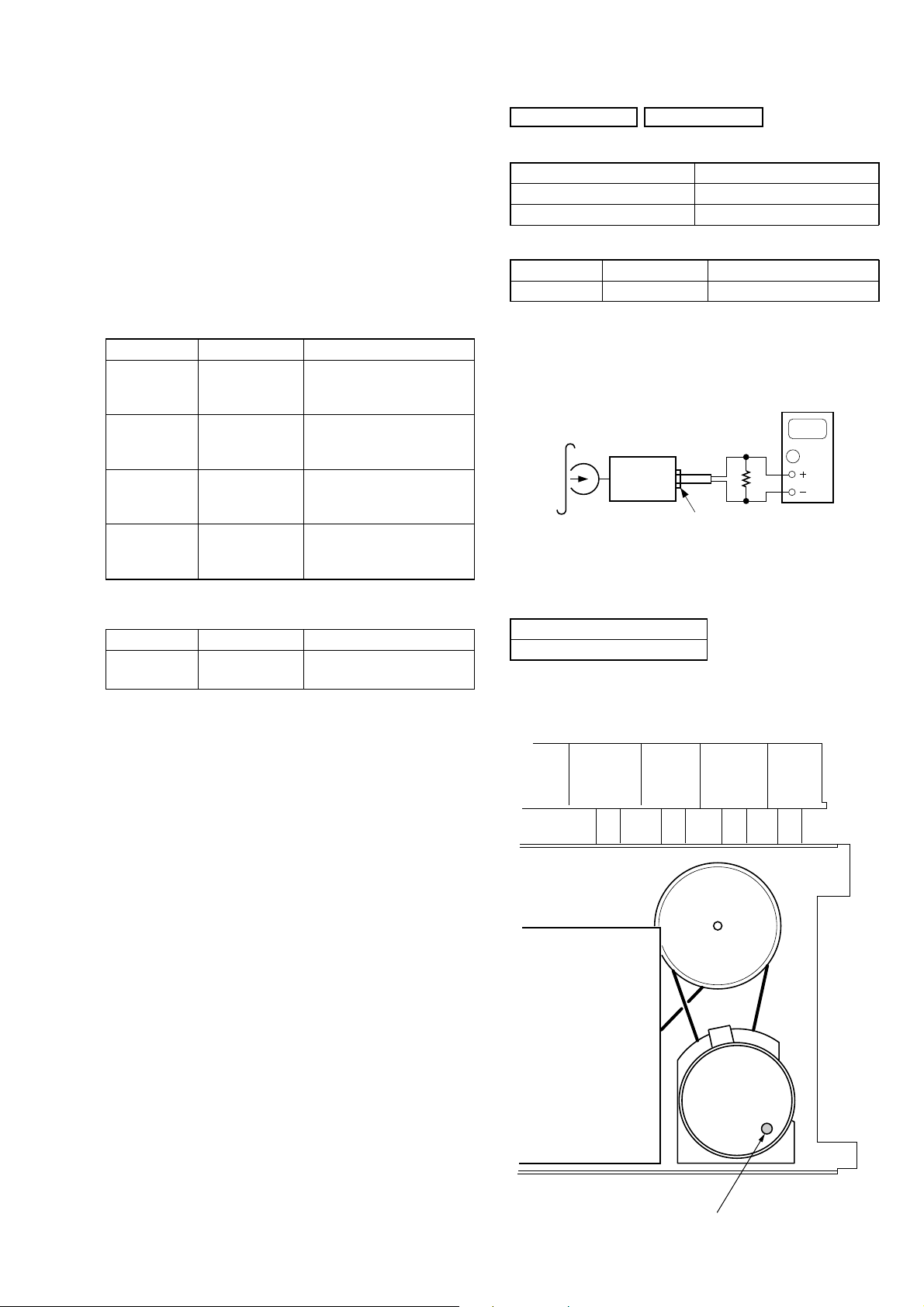
Torque Measurement
Mode Torque meter Meter reading
2.95 – 6.86 mN • m
FWD CQ-102C (30 – 70 g • cm)
(0.42 – 0.97 oz • inch)
FWD
Back Tension
FF CQ-201B (more than 60 g • cm)
REW CQ-201B (more than 60 g • cm)
CQ-102C (1.5 – 5.5 g • cm)
0.15 – 0.53 mN • m
(0.021 – 0.076 oz • inch)
more than 5.88 mN • m
(more than 0.83 oz • inch)
more than 5.88 mN • m
(more than 0.83 oz • inch)
TAPE SECTION 0 dB = 0.775 V
• Standard Output Level
Output terminal HP OUT
load impedance 32 Ω
output signal level 0.25 V (–10 dB)
• Test Tape
Type Signal Used for
WS-48A 3 kHz, 0 dB tape speed adjustment
Tape Speed Adjustment
Procedure:
Mode: playback
test tape
WS-48A
(3 kHz, 0 dB)
set
i
jack (J321)
Adjust so that the value on the digital frequency counter is
3,000 Hz.
digital frequency
counter
Ω
32
Tape Tension Measurement
Mode Tension meter Meter reading
FWD CQ-403A
more than 100 g
(more than 3.53 oz)
Specification Value:
Digital frequency counter
2,910 to 3,090 Hz
Adjust so that the frequency at the beginning and that at the end of
tape winding are between 2,910 to 3,090 Hz.
Adjustment Location:
Tape speed adjustment
control inside motor
13
CFD-S03CP/S03CPL
r
r
Ver. 1.2
TUNER SECTION 0 dB = 1 µV
[AM (MW/LW)]
Setting:
Function: RADIO/BAND/AUTO PRESET
Band: MW or LW
AM RF signal
generator
30% amplitude
modulation by
400 Hz signal
Output level:
as low as possible
[FM]
Setting:
Function: RADIO/BAND/AUTO PRESET
BAND button: FM
FM RF signal
generator
75 kHz frequency
deviation by 1 kHz
signal
Output level:
as low as possible
• Connecting Digital Voltmeter (FM, MW and LW)
Put the loop
antenna close to
the set.
set
MAIN board
TP ANT2 (JW231, 232)
0.01 µF
set
32
Ω
i
jack (J321)
Ω
32
i
jack (J321)
level mete
level meter
AM (MW/LW) IF ADJUSTMENT
Adjust for a maximum reading on level meter
T1 450 kHz
LW FREQUENCY COVERAGE ADJUSTMENT (AEP)
Adjustment Part Frequency Display Reading on Digital Voltmeter
L3 279 kHz 5.3 ± 0.5 V
Confirmation 153 kHz 0.6 ± 0.05 V
+
–
+
–
ANT1-2 162 kHz
Adjustment Part Frequency Display Reading on Digital Voltmeter
Confirmation 531 kHz 0.9 ± 0.2 V
Confirmation 1,611 kHz 5.5 ± 0.5 V
Adjustment Part Frequency Display Reading on Digital Voltmeter
Confirmation 1,611 kHz 5.0 ± 0.5 V
MW FREQUENCY COVERAGE ADJUSTMENT (CND, E92, MX)
Adjustment Part Frequency Display Reading on Digital Voltmeter
Confirmation 1,710 kHz 5.8 ± 0.05 V
MW TRACKING ADJUSTMENT (EXCEPT CND, E92, MX)
ANT1-1 621 kHz
LW TRACKING ADJUSTMENT (AEP)
Adjust for a maximum reading on level meter
CT5 261 kHz
MW FREQUENCY COVERAGE ADJUSTMENT (AEP)
MW FREQUENCY COVERAGE ADJUSTMENT
(EXCEPT CND, AEP, E92, MX)
L3 531 kHz 0.8 ± 0.05 V
L3 530 kHz 0.8 ± 0.5 V
Adjust for a maximum reading on level meter
CT3 1,404 kHz
digital voltmete
MAIN board
100 k
TP (VT)
TP (GND)
Ω
•Repeat the procedures in each adjustment several times, and the
tracking adjustments should be finally done by the trimmer
capacitors.
• Remove FM antenna in FM adjustment.
MW TRACKING ADJUSTMENT (CND, E92, MX)
Adjust for a maximum reading on level meter
ANT1-1 620 kHz
CT3 1,400 kHz
FM IF ADJUSTMENT
Adjust for a minimum reading on level meter
L6 10.7 MHz
FM FREQUENCY COVERAGE ADJUSTMENT
Adjustment Part Frequency Display Reading on Digital Voltmeter
L2 108 MHz 3.0 ± 0.2 V
Confirmation 87.5 MHz 1.5 ± 0.5 V
FM TRACKING ADJUSTMENT
Adjust for a maximum reading on level meter
L1 87.5 MHz
CT1 108 MHz
Adjustment and Connecting Location:
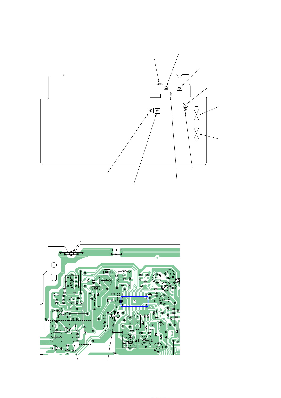
MAIN board (See page 15)
•Abbreviation
CND : Canadian model
E92 : AC 120V area in E model
MX : Mexican model
14
Adjustment Location:
G
CFD-S03CP/S03CPL
– MAIN BOARD (Component Side) –
L6: FM IF ADJUSTMENT
L2: FM FREQUENCY
COVERAGE
ADJUSTMENT
IC1
T1: AM (MW/LW)
IF ADJUSTMENT
CT1: FM TRACKING
ADJUSTMENT
L3: AM (MW/LW)
FREQUENCY COVERAGE
ADJUSTMENT
ANT1
CT3: MW TRACKING
ADJUSTMENT
L1: FM TRACKING
ADJUSTMENT
CT5: LW TRACKING
ADJUSTMENT
ANT1-1: MW TRACKIN
ADJUSTMENT
ANT1-2: LW TRACKING
ADJUSTMENT
Test Point:
– MAIN BOARD (Conductor Side) –
JW232
JW231
L3
C14
C10
JW226
C15
C13
C60
C63
C62
C61
R32
C64
Q33
R37
R5
C55
Q35
R34
R36
C69
C68
C51
R31
C11
C12
R6
D3
C9
C53
CT5
C54
CT3
Q32
TP ANT2
JW224
JW223
R2
R11
D1
C3
R38
JW217
JW218
JW219
R35
R30
D5
D4
D2
CT1
C2
R1
C67
C1
L1
C21
C70
C29
JW220
JW207
C22
C6
R26
JW209
C72
L2
C5
R3
C7
R7
C4
C23
JW208
C24
CF3
C25
T1
R9
C16
R4
R13
C45
R12
R15
X1
IC1
R28
C33
C27
CF2
JW188
C26
R25
R41
C28
R29
L6
C17
C19
R14
C46
C18
R27
R39
C20
C42
C41
C40
R20
C34
D6
C35
C39
R18
C38
E92,MX
MODEL
R16
C30
C37
R22
R17
JW191
JW187
R21
R23
JW2
R19
C31
C32
R10
TP (VT) TP (GND)
15
CFD-S03CP/S03CPL
CD SECTION
CD section adjustments are done automatically in this set.
In case of operation check, confirm that focus bias.
FOCUS BIAS CHECK
1. Connect the oscilloscope between IC201 pin u; and pin th (or
TP (RFAC0) and TP (VC)).
2. Insert the disc (PATD-012 (Tr 15)). (Part No. : 4-225-203-01)
3. Press the N X (CD) button.
4. Confirm that the oscilloscope waveform is as shown in the figure
below. (eye pattern)
A good eye pattern means that the diamond shape ( ) in the
center of the waveform can be clearly distinguished.
• RF signal reference waveform (eye pattern)
VOLT/DIV : 50 mV (10 : 1 probe in use)
TIME/DIV : 500 nS
RF level :
+0.3
1.1 Vp-p
–0.2
When observing the eye pattern, set the oscilloscope for AC range
and raise vertical sensitivity.
Test Point:
– BD83S BOARD (Conductor Side) –
C292
C291
R292
R278
3
3
C218
100
1
30
R291
R270
C214
C217
IC201
31
C224
TEI
R252
VC
C251
C252
C213
R253
FEI
R255
C222
91
90
61
60
R254
C253
B9
C221
RFACI
R258
R250
RFACO
C208
C254
TP (RFAC0)TP (VC)
R257
C261
R267
R268
C260
C258
C256
1-868-067-
APC
C303
R265
C230
C264
C301
R266
C265
C273
C304
11
(11)
CN301
16
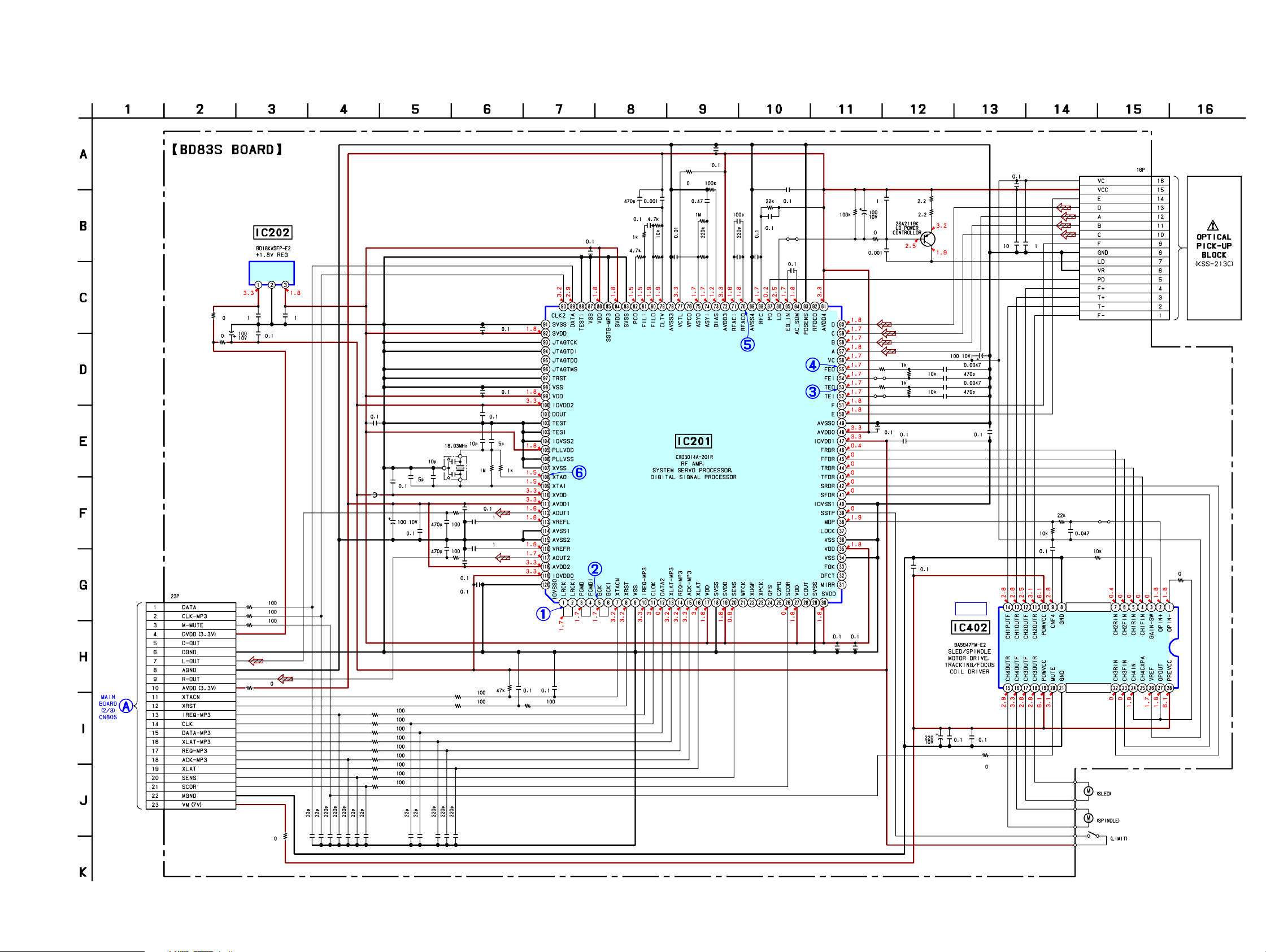
SECTION 6
DIAGRAMS
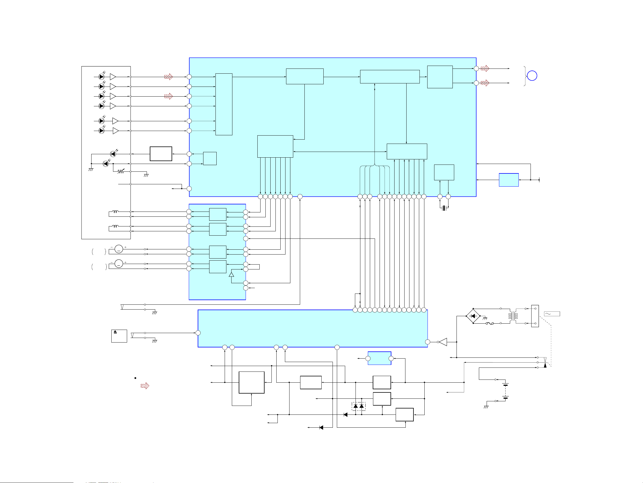
6-1. BLOCK DIAGRAM — CD SECTION —
A
B
C
D
A
B
C
D
57
58
C
59
D
60
CFD-S03CP/S03CPL
AOUT1
112
A
B
PRI-
SERVO
AMP
SYNCHRONOUS
CIRCUIT
DSP
DAC
AOUT2
117
CD_IN_ L
CD_IN_R
A
(Page 18)
E
F
LD
PD
OPTICAL PICK-UP
BLOCK
(KSS-213C)
TRACKING
COIL
FOCUS
COIL
M402
SLED
MOTOR
M401
SPINDLE
MOTOR
(LIMIT)
S201
E
F
LD
PD
VR
VC
M
M
VC
T+
T–
F+
F–
LD POWER
CONTROLLER
Q321
SL+
SL–
SP+
SP–
VC
50
51
66
67
56
13
14
12
11
17
18
16
15
E
F
LD
PD
VC
CH1OUTR
CH1OUTF
CH2OUTF
CH2OUTR
CH3OUTF
CH3OUTR
CH4OUTF
CH4OUTR
APC
TRACKING
COIL
DRIVE
FOCUS
COIL
DRIVE
SLED
MOTOR
DRIVE
SPINDLE
MOTOR
DRIVE
SLED/SPINDLE
MOTOR DRIVER,
TRACKING/FOCUS
COIL DRIVER
IC402
CH1INR
CH1INF
CH2INF
CH2INR
MUTE
CH3INF
CH3INR
CH4IN
OPOUT
OPIN+
VREF
DIGITAL
SERVO
CONTROL
TRDR
TFDR
FFDR
FRDR
SFDR
SRDR
MDP
44 43
45 46 41 42 38 39
5
4
6
7
20
23
22
24
27
2
VC
26
SSTB
RF AMP,
SYSTEM SERVO PROCESSOR,
DIGITAL SIGNAL PROCESSOR
IC201
7
I/F
XLAT
XTACN
ACK-MP3
IREQ-MP3
REQ-MP3
XLAT-MP3
CLK2
DATA2
12 90 13 15 891671014 11 20 109 10826 8
27
12
11
10
6
5
28 26
DATA
CLOK
31 30 29 43 4
8
SENS
SCOR
XRST
CLOCK
GENERATOR
XTAO
XTAI
X201
16.93MHz
VDD (3.3V)
VDD (1.8V)
+1.8V REG.
IC202
T901
POWER
TRANSFORMER
CD3.3V
J901
AC IN
CFD-S03CP/S03CPL
SW2
PUSH
OPEN/
CLOSE
Signal path
: CD
LID-OPEN
18
CD 6V
CD 3.3V
REG-CHK23I-CD-CTL
36
+3.3V
REC/PB
POWER
CONTROL
Q957-959,D957
(TAPE)
RADIO +B
SYSTEM CONTROLLER
IC801 (1/2)
BAT-CHK-H
V-CHECK
37
38
RIPPLE
FILTER
Q304
9V (SW)
6V
R-VT
D324
O-POWER
1
D951
D952
I-DATA-MP3
3.3V
O-CLK-MP3
O-DATA-MP3
O-RQ-MP3
O-XLAT-MP3
O-STBY-MP3
+3.3V REG
IC804,Q802
AUDIO+6V
REG
Q955,D953
POWER
SWITCH
Q952,953
I-RQ-MP3
I-ACK-MP3
45
I-CD-XLAT
O-CD-CMD
O-CD-XTACN
POWER
SWITCH
Q951
O-CD-CLK
I-CD-SENS
AC-CHK
VDD
CD-XRST
I-CD-SCOR
45
Q801
AC-HI
U-COM
(VDD)
D901 – 904
RECT
BATT
F902
DRY BATTERY
SIZE "D"
(IEC DESIGNATION R20)
6PCS, 9V
17 17
CFD-S03CP/S03CPL
Ver. 1.1
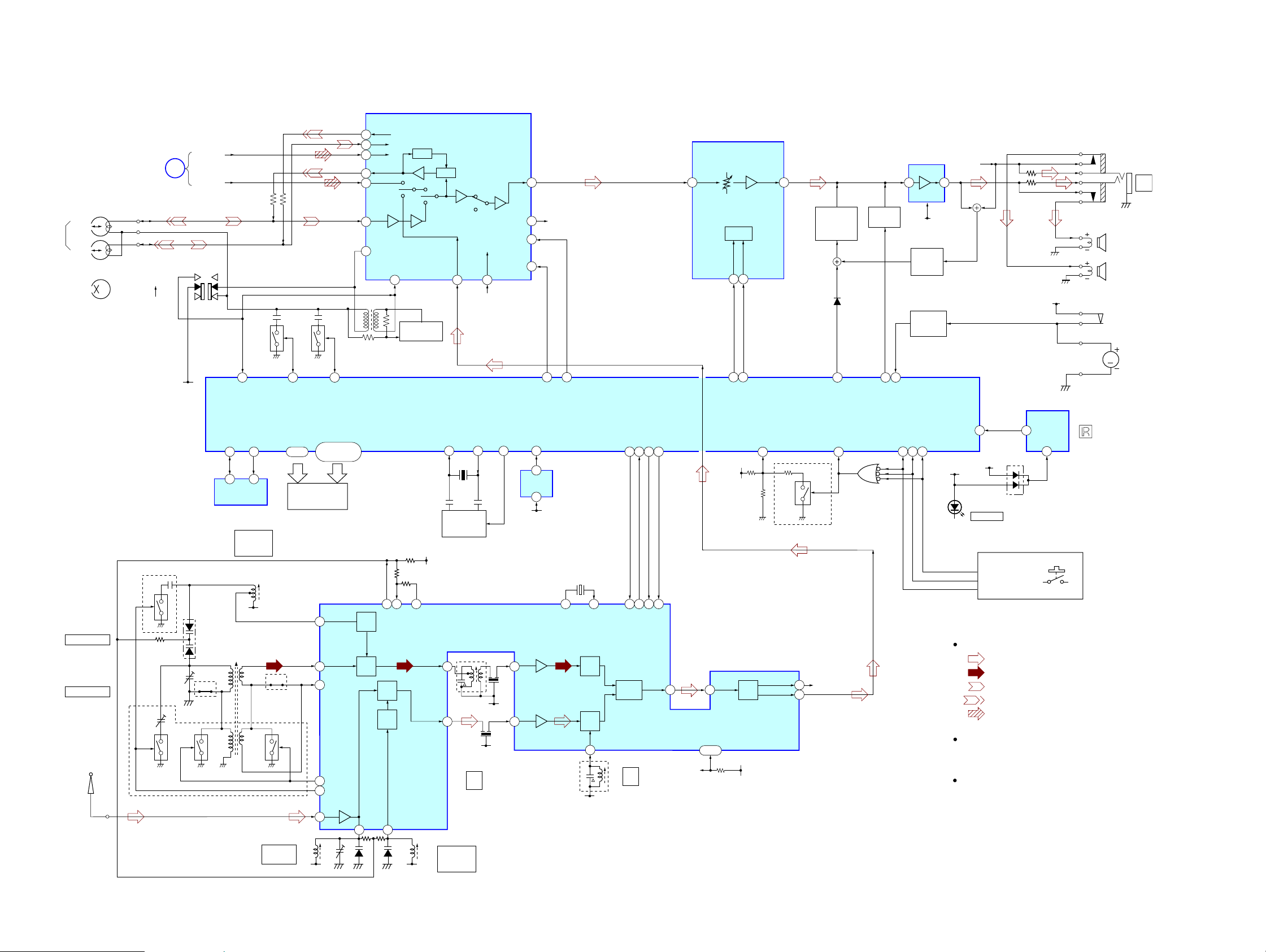
6-2. BLOCK DIAGRAM — MAIN SECTION —
HRP301
RECORD/PLAYBACK
HEAD
L-CH
R-CH
HE301
ERASE HEAD
ANT1-1,CT3
MW TRACKING
ANT1-2,CT5
LW TRACKING
ANT2
FM
TELESCOPIC
ANTENNA
(Page 17)
S301
(REC/PB)
REC
PB
AEP MODEL
Q33
CT5
AEP MODEL
A
+B
6V (TAPE)
CT3
CD_IN_R
CD_IN_L
-1 -2
D3
JC3
EXCEPT
AEP
MODEL
25
TAPE REC
SAD
EEPROM
IC802
MW/LW
FREQUENCY
COVERAGE
RADIO 5V
ANT1
MW/LW
FERRITE-ROD
ANTENNA
-1
-2
SCL
4746
65
L3
L3
Q302
JC4
EXCEPT
AEP MODEL
Q31Q32Q35
CT1,L1
FM
TRACKING
Q303
49
ISS1
COM1|COM4
97–94,89–67,
62–59
LIQUID CRYSTAL
DISPLAY PANEL
LCD401
31
1
2
29
30
36
L1 CT1
RADIO 5V
50
S1
64,63
AM OSC
AM RF-IN
REG
BO1
BO2
FM
RF-IN
ISS2
|
S29
(VT)
D1
R.RO
9
R.IN
8
14
4
24
5
6
T301
AM
OSC
AM
MIX
FM
RF-OUT
R.LIN
L.RO
L.LIN
L.IN
REF
MIX
OSC
DET
REC
21 22 16
REC BIAS OSC
Q301
28
27PD26
LP-IN
LP-OUT
AM
MIX-OUT
FM
FM
FM
MIX-OUT
FM OSC
3234
D2
RADIO 5V
ALC 2
RADIO L
L.RAD
TU_IN_L
SYSTEM CONTROLLER
IC801 (2/2)
93X092
X802
4.19MHz
FREQUENCY
EXCHANGE
SWITCH
R-VT
FM/MW/LW FRONT-END,
IF AMP, DET, FM MPX
5 7
3
L2
FM
L2
FREQUENCY
COVERAGE
REC/PB
PRE AMP
IC301
TU_IN_R
X1
IC1
T1
RADIO 5V
RADIO 5V
T1
AW
IF
R.RAD
FM/AM SHIFT
2
CF3
CF2
L.LO
R.LO
LINE
TAPE
8
AM
IF-IN
FM
IF-IN
20
18
17
15
54
1
RESET
IC805
2
3.3V
R-CH
TAPE
CD
57
TAPE
CD-ON
RESET
X1
75kHz
20 19 16 17CE15
X IN
X OUT
AM
DET
FM
DET
FM-DET
11
L6
RADIO 5V
21 20 1922
AF
BUFFER
L6
FM
IF
O-TU-DATA
I-TU-COUNT
O-TU-CLK
18
DI
CL
DO
DET-OUT
IC302
ELECTRONIC VOLUME
VCC
6,33
MPX-IN
LOGIC
5
3455 33
3.3V
VOL AMP
CLK4DATA
VOL-CLK
L-IN
8 7
O-TU-CE
23 22
RADIO 5V RADIO+B
L-OUT
VOL-DATA
I-SUFFIX
48
AEP,AUS,AR,KR,TW MODEL
R-OUT
FM
L-OUT
MPX
POWER AMP
MEGA
BASS
SWITCH
Q122
D322
MUTE
Q124
IC303
6 2
U-COM
(VDD)
LEVEL
DETECT
D323
TAPE PLAY
DETECT
Q808
R-CH
9V (SW)
SP101
SPEAKER
(L-CH)
SP201
SPEAKER
(R-CH)
SW1
(TAPE PLAY)
J321
i
M
17
M-BASS
WAKE-UP
42
Q806
Q805,D801,802
3
24
A-MUTE
TAPE-PLAY
I-KEY241I-KEY140I-KEY0
39
9V (SW)
KEY0
KEY1
KEY2
I-RMC
AC-HI
D406
OPR/BATT
S401–407
S411,413–417
S421–424
REMOTE
CONTROL
19
RECEIVER
D461
KEY NETWORK
IC401
3
M901
CAPSTAN/REEL
MOTOR
Signal path
: FM
: AM
TU_IN_R
13
12
: TAPE PLAY
: TAPE REC
: CD
R-ch is omitted due to same as
L-ch.
Abbreviation
AUS : Australian model
AR : Argentina model
KR : Korea model
TW : Taiwan model
CFD-S03CP/S03CPL
1818
6-3. CIRCUIT BOARDS LOCA TION • NOTE FOR PRINTED WIRING BOARDS AND SCHEMATIC DIAGRAMS
THIS NOTE IS COMMON FOR PRINTED WIRING BOARDS AND SCHEMATIC DIAGRAMS.
(In addition to this, the necessary note is printed in each block.)
HEADPHONE board
KEY-1 board
PANEL board
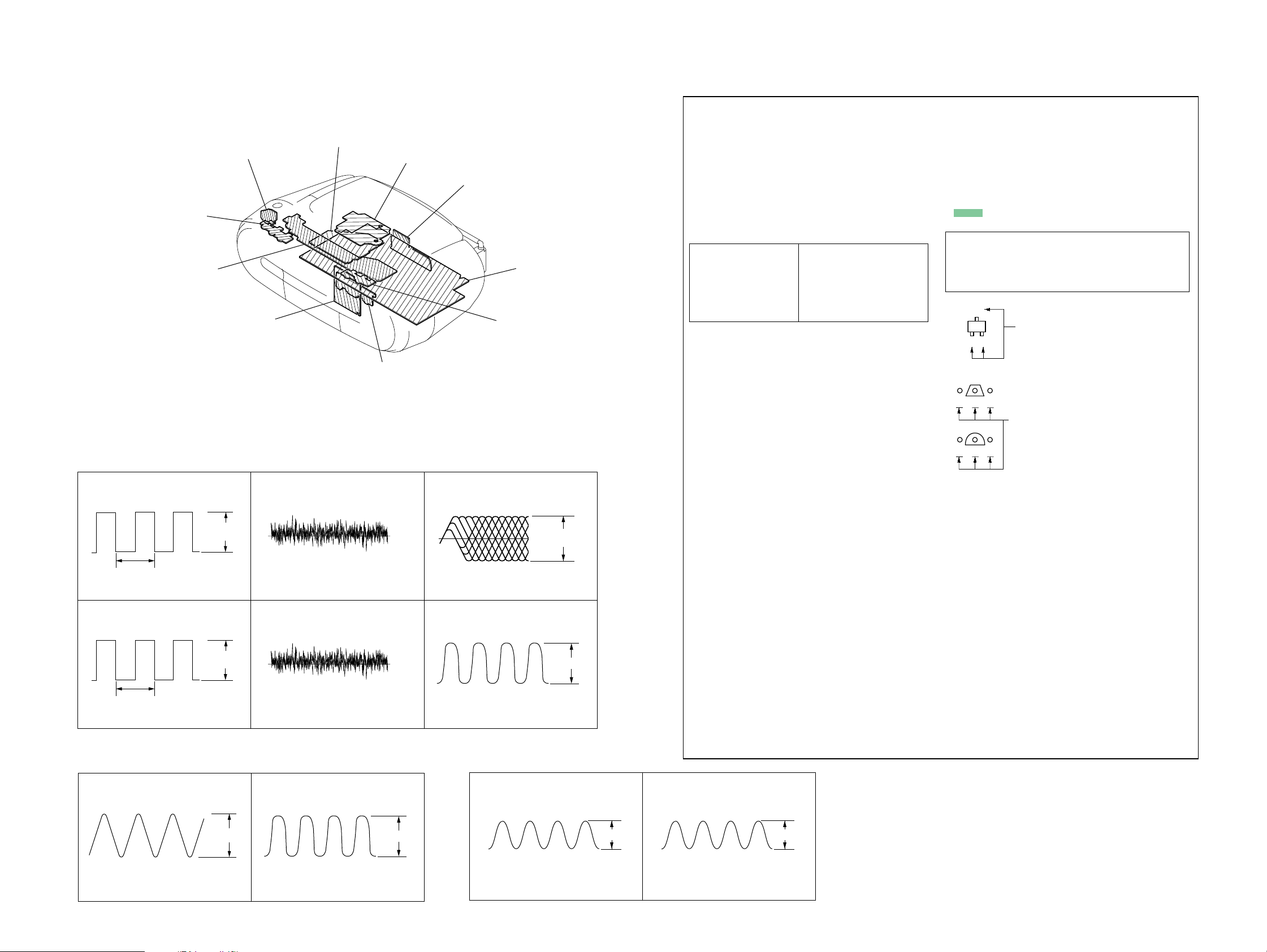
• Waveforms
— BD83S Board — (CD PLAY)
1
IC201 1 (LRCK)
3.2 Vp-p
22.6 µsec
2
IC201 5 (BCK)
3.2 Vp-p
0.47 µsec
1 V/div, 200 nsec/div
— MAIN Board —
TC board
3
IC201 td (TEO)
1 V/div, 5 msec/div1 V/div, 10 µsec/div
4
IC201 tg (FEO)
100 mV/div, 5 msec/div
POWER board
BATTERY-2 board
Approx. 1 Vp-p
Approx. 150 mVp-p
BD83S board
5
1.7 V
500 mV/div, 0.5 µsec/div
6
1.7 V
1 V/div, 20 nsec/div
BATTERY-1 board
KEY-2 board
IC201 u; (RFACO)
IC201 <z/, (XTAO)
16.95 MHz
— TC Board — (REC)
MAIN board
+0.3
1.1 Vp-p
–0.2
3.3 Vp-p
For schematic diagrams.
Note:
• All capacitors are in µF unless otherwise noted. (p: pF)
50 WV or less are not indicated except for electrolytics
and tantalums.
• All resistors are in Ω and 1/
specified.
• f : internal component.
• C : panel designation.
Note:
The components identified by mark 0 or dotted
line with mark 0 are criti-
cal for safety.
Replace only with part
number specified.
• A : B+ Line.
• H : adjustment for repair.
•Voltages and waveforms are dc with respect to ground
under no-signal (detuned) conditions.
– BD83S Board –
no mark : CD PLAY
– MAIN (1/3) Board –
no mark : FM
(): AM
– MAIN (2/3), (3/3) and Other Boards –
no mark : FM
(): PB
<>: REC
[]: CD PLAY
•Voltages are taken with a VOM (Input impedance 10 MΩ).
Voltage variations may be noted due to normal production
tolerances.
•Waveforms are taken with a oscilloscope.
Voltage variations may be noted due to normal production
tolerances.
• Circled numbers refer to waveforms.
• Signal path.
F : FM
f : AM
E : PB
a : REC
J : CD PLAY
• Abbreviation
CND : Canadian model.
CET : East European & Russian model.
E41 : AC 230V area in E model.
E92 : AC 120V area in E model.
AUS : Australian model.
KR : Korea model
MX : Mexican model.
SP : Singapore model.
IT : Italian model.
AR : Argentina model.
TH : Thai model.
TW : Taiwan model.
4
W or less unless otherwise
Note:
Les composants identifiés par
une marque 0 sont critiques
pour la sécurité.
Ne les remplacer que par une
piéce portant le numéro
spécifié.
For printed wiring boards.
Note:
• X : parts extracted from the component side.
• Y : parts extracted from the conductor side.
• W : indicates side identified with part number.
f
•
• : Pattern from the side which enables seeing.
Caution:
Pattern face side: Parts on the pattern face side seen from
(Conductor Side) the pattern face are indicated.
Parts face side: Parts on the parts face side seen from
(Component Side) the parts face are indicated.
• Abbreviation
: internal component.
(The other layers' patterns are not indicated.)
C
Q
B
E
Q
BCE
Q
B
C
CND : Canadian model.
CET : East European & Russian model.
E41 : AC 230V area in E model.
E92 : AC 120V area in E model.
AUS : Australian model.
KR : Korea model
MX : Mexican model.
SP : Singapore model.
IT : Italian model.
AR : Argentina model.
TH : Thai model.
TW : Taiwan model.
These are omitted.
These are omitted.
E
CFD-S03CP/S03CPL
Ver. 1.2
1 IC1 w; (X OUT)
1 V/div, 5 µsec/div
CFD-S03CP/S03CPL
75 kHz
2.2 Vp-p
2 IC801 os (X1)
4.13 MHz (AM)
4.17 MHz (EXCEPT AM)
1 V/div, 100 nsec/div
3.4 Vp-p
1
Q301 C
18.2 µsec
1 V/div, 10 µsec/div
2
3.5 Vp-p
10 V/div, 10 µsec/div
19 19
HRP301 (YEL)
35 Vp-p
18.2 µsec
CFD-S03CP/S03CPL
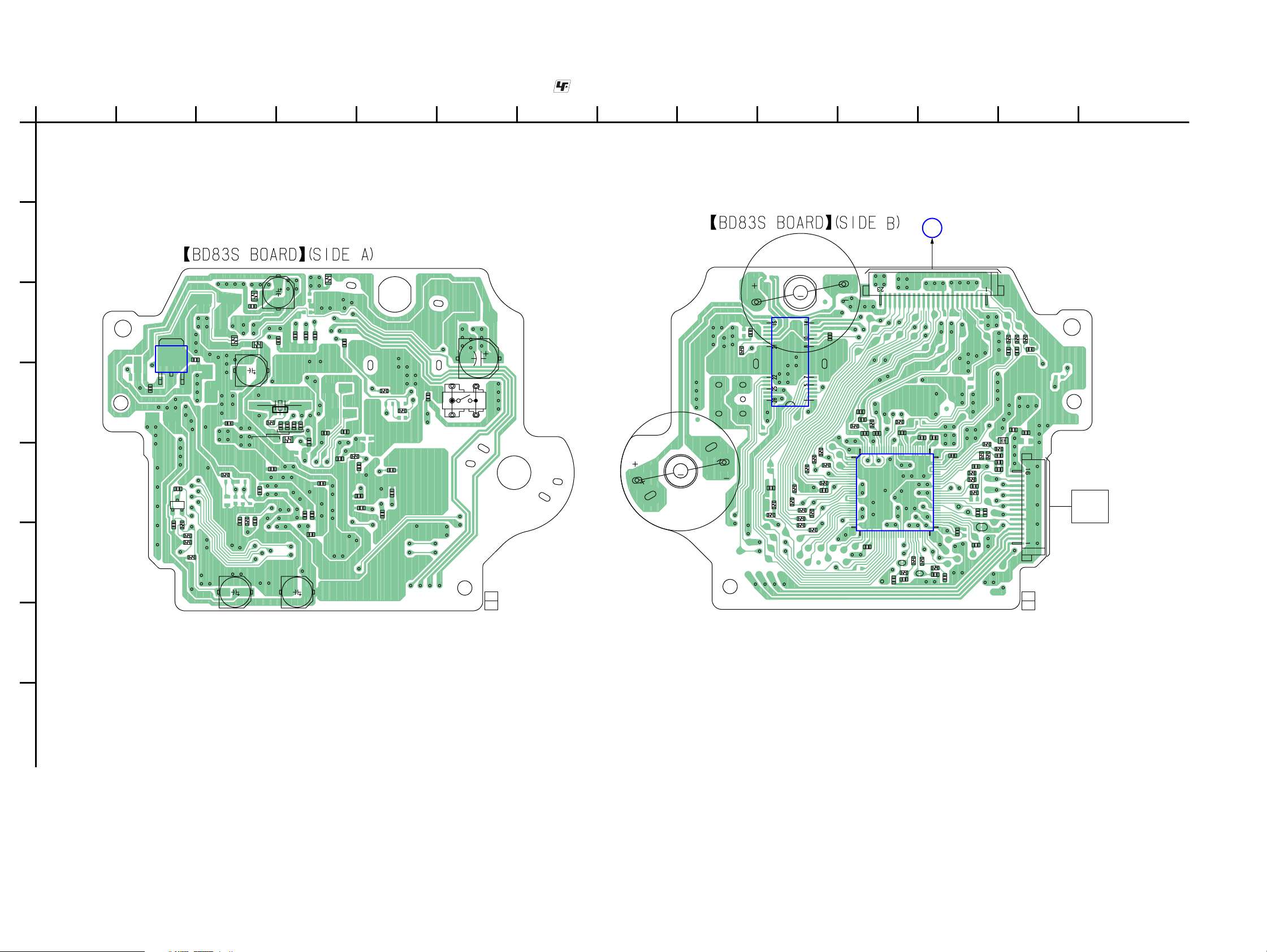
6-4. PRINTED WIRING BOARD — BD83S SECTION —
1
234567891011 12 13 14
A
B
R201
C201
C202
C
R202
D
E
IC202
1
C226
2
C321
B
Q321
C322
R322
R321
R207
C227
3
C
E
R323
R324
C204
R260
C274
C203
R256
R271
C266
C210
C257
C267
C223
X201
C275
C110
C268
C108
R203
F
C323
C207
• Refer to page 19 for Circuit Boards Location. : Uses unleaded solder.
R401
C219
C277
R276
C424
C271
C105
C107
R423
C272
C109
C104
R421
C406
(LIMIT)
1-868-067-
S201
C401
(11)
(SPINDLE)
11
C206
C205
C102
C101
C276
C215
C220
C232
(Page 22)
MAIN BOARD
CN805
A
M402
(SLED)
R270
TEI
C214
R252
C252
C213
R253
FEI
CN102
R255
60
R254
C253
C222
91
B9
90
RFACI
61
C221
RFACO
C254
R258
R250
R257
C208
C261
R267
R268
C260
C258
C256
1-868-067-
APC
C303
R265
C264
C230
C301
R266
C265
C273
R112
C112
R113
C113
C304
(11)
C111
11
R111
CN301
OPTICAL
PICK-UP
BLOCK
(KSS-213C)
M
B8
C405
R280
B7
MM
401
M
C451
R452
R451
R109
R107
R104
IC402
R105
R102
R110
R101
R277
R103
C103
R108
B10
C404
R275
R278
R292
C291
C218
1
30
100
C292
31
C224
VC
C217
R291
IC201
C251
G
H
CFD-S03CP/S03CPL
2020
CFD-S03CP/S03CPL
6-5. SCHEMATIC DIAGRAM — BD83S SECTION —
IC202
R207
R202
C226
C203
C227
C204
• Refer to page 19 for Waveforms. • Refer to page 32 for IC Block Diagram. • Refer to page 34 for IC Pin Description of IC201.
C210
R260 R257
C223
R203
C215
C275
C268
X201
R271
C222
C213
C214
C264
C273
C265 R265
C221
C267C266
R270
R266
R267
R268
C261
C260
R250
IC201
R258
C230
C258
C274
R256
C257
C208
TP1
C256
R324
C323
R323
C321
C322
TP4
TP3
C206
R255
R253
Q321
C205
R321
R322
C207
R254
R252
C254
C253
C252
C251
C232
C301
C303 C304
CN301
(Page 24)
CN102
R113
R112
R111
R201
R401
C113
C112
C111
C110
C108
C102
C101
R110
R103
R105
R104
R109
R108
R107
R102
R101
C201
C202
C103
C105
C291
C292
C104
C109
R291
R292
C107
C218
C219
R275
R277
C217
C276
C277
R276
C272
R278
C271
R451
R452
C424
C404
TP2
C451
R423
R421
IC B/D
C224C220
C401
IC402
C405 C406
R280
M402
M401
S201
CFD-S03CP/S03CPL
21 21
CFD-S03CP/S03CPL
Ver. 1.4
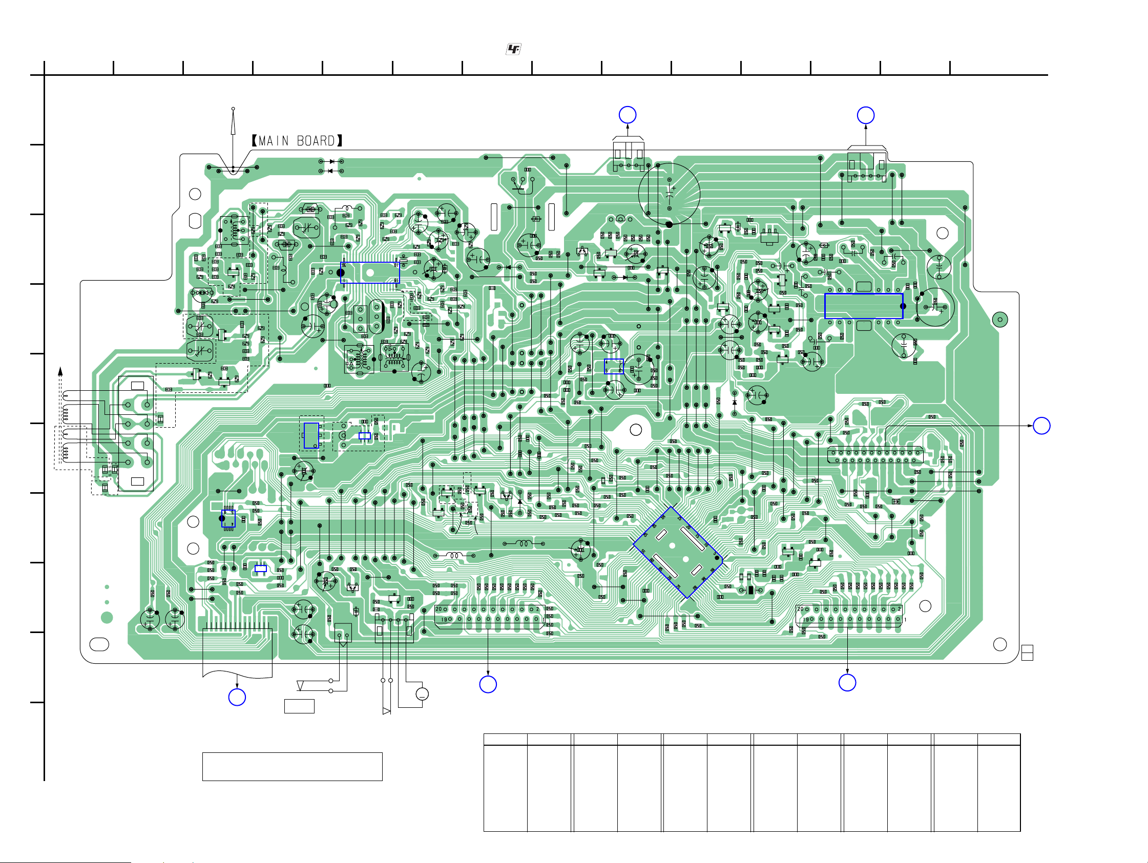
6-6. PRINTED WIRING BOARD — MAIN SECTION —
• Refer to page 19 for Circuit Boards Location. : Uses unleaded solder.
1
A
B
C
D
ANT1
MW/LW
FERRITE BAR
ANTENNA
E
-1
-2
F
AEP MODEL
JC2
JC1
EXCEPT AEP
MODEL
JC3
G
H
I
J
CFD-S03CP/S03CPL
234567891011 12 13 14
ANT1
R161
C161
C52
R261
ANT2
FM TERESCOPIC
ANTENNA
(Page 30)
POWER BOARD
CN901
E
JW167
C951
JW108
JC804
JW230
JW189
JW229
R481
R482
R836
JW212
JW213
R837
Q955
D324
JW227
D802
R820
R838
JW110
JW185
JW228
R830
R839
JW170
R476
C822
L804
R840
C953
R326
R325
JW206
D801
R841
D953
C952
R955
JW175
JW184
C823
R894
R829
R842
JW174
JW183
JW205
R823
JW204
R843
R331
C821
R891
R954
JW139
JW143
R896
R822
R844
R845
R846
R847
JW172
JW180
C349
C350
R332
JW202
C807
JW168
R960
JW201
JW171
R335
R892
R811
R821
R492
D951
R336
JW178
R477
R825
Q951
C311
R338
R337
R479
R888
C808
D
• Semiconductor Location
Ref. No. Location
D1 C-4
D2 B-4
D3 D-3
D4 B-5
D5 B-5
D6 C-6
D322 E-10
D323 C-12
D324 C-7
Ref. No. Location
D461 H-5
D462 H-5
D801 G-7
D802 G-7
D951 C-8
D952 C-9
D953 C-8
D957 C-10
JW197
R818
R956
JW135
JW177
JC103
JW198
R491
R953
Q953
C213
R816
R889
R490
JW199
13
CN305
Q952
E
R952
R964
R951
BBCCE
R957
C358
D952
C217
C330
IC302
C113
C117
JW196
JW181
R478
R810
R815
R824
50
51 80
R488
JW200
R963
JW126
R962
C956
Q304
JW136
C353
R329
R819
JW176
C815
R961
R330
C814
JW125
BCE
JW141
R321
R328
JW149
JW166
31
JW179
JW169
JW148
R812
R809
R851
JW133
JW140
JW165
30
IC801
R852
C325
JW127
JW132
JW106
JW107
JW164
R853
R958
R333
81
JW131
JW138
JW145
JW163
R854
JW142
JW137
JW144
JW162
C959
C357
R475
JW161
C819
Q958
BCE
JW129
Q959
BCE
C215
C115
JW195
C813
1
100
R868
R959
R817
D322
R235
R234
R134
D957
R236
C127
JW146
R135
JW159
R804
C961
C229
C227
JC102
X802
R965
C129
JW190
JC101
C957
R240
R247
C232
C225
R138
C132
C331
JW158
R831
C818
C811
C452
R140
R136
R327
Q957
C125
C454
CE
R238
Q222
Q122
BCE
R805
Ref. No. Location Ref. No. Location
IC1 C-5
IC302 E-9
IC303 D-12
IC801 G-10
IC802 G-3
IC804 F-5
IC805 H-4
IC806 F-4
Q31 E-3
Q32 E-3
Q33 C-3
Q35 D-3
Q122 D-11
Q124 E-11
Q222 D-11
Q224 C-11
Q304 C-9
B
JW157
R801
C456
C451
C230
BCE
R241
BCE
R147
CE
Q124
JW155
Q452
JW160
B
JW156
C453
R850
JW134
Q224
R239
C206
JW130
R139
C106
R141
JW154
BCE
C455
JW128
C208
+
C131
R451
R803
C323
C130
JW153
R453
C458
Q451
R849
C231
R242
R142
C457
JW105
D323
R323
+
JW151
BCE
R855
R848
D2
CT1
C21
C70
C29
IC806
JW244
JW207
C67
C22
1
2
3
C805
C72
C461
C6
R26
JW209
JW242
R463
R493
D5
D4
C4
C23
C24
C
JW240
CN806
L2
C5
R3
C7
R7
CND,E92,MX
MODEL
JW208
CF3
C25
T1
C803
E
54
Q802
1
B
IC804
TYPE A
JW225
JW239
R462R461
D461
JC807
D462
R4
IC1
3
JW238
C16
R13
CF2
JW257
R897
(LEAF SW)
R12
C28
R883
JW237
SW1
R9
C45
R15
X1
R28
C27
C26
R25
R29
L6
R884
R828
JW236
JW221
Q808
C817
BCE
R899
CN304
(CAPSTAN/REEL MOTOR)
C33
R41
JW235
14
C41
C34
C31
C40
C30
C42
C32
R10
JW216
JW234
MM
M801
C19
R39
R20
R19
R480
R467
JW222
C18
JW188
R16
AEP,AUS,
KR,AR,TW
MODEL
JW215
Q801
R465
C17
C46
R27
C20
D6
C39
C35
R18
C38
C37
R22
R17
JW191
JW211
CND,AEP,E92,AUS,
MX,KR,AR,TW MODEL
Q806
JW214
UK,E41,CET,
IT,SP,TH
MODEL
L803
R464
R466
C43
JW187
R21
R23
JW203
JW194
JW210
R483
R898
R802
R14
R24
JW193
R826
AEP,AUS,
KR,AR,TW
MODEL
C326
C36
JW192
JW233
Q805
R827
R835
CN804
PANEL BOARD
FFC401
(Page 28)
JW232
JW231
AEP MODEL
L3
C14
C10
IC802
C62
C61
R5
JW226
R32
C63
Q35
C13
C51
Q31
JW254
Q33
R37
JW256
R486
FFC802
R34
R36
C69
C68
C15
R471
R472
C64
C55
R31
R870
R869
C820
JW255
C11
C12
R6
D3
C9
C53
CT5
C54
CT3
Q32
AEP MODEL
JC4
R487
R474
R473
JW246
JW247
C261
14
B
TC BOARD
CN301
C60
JW217
JW218
C825
IC805
JW224
R11
R38
JW219
R35
R30
JW223
R484
13
54
1
R2
D1
C3
R886
R885
C2
R1
L1
JW220
JW249
JW250
C806
OPEN/CLOSE
C1
JW245
JW248
C262
C162
SW2
Z/PUSH
TYPE B
JW241
C804
(Page 26)
Refer to NOTE FOR REPLACEMENT OF THE
IC804 AND IC806 on page 4 for type A and B.
2222
(Page 26)
HP BOARD
CN307
F
14
CN306
JW102
R245
CN805
C836
R860
R875
R861
R874
JW121
JW150
R862
+
R145
FB832
R863
JW103
164 3
+
C119
JW147
R864
JW116
C212
C354
C816
R865
JW117
FB831
R866
C356
R144
C110
JW186
JW124
R262
JW119
JW120
R887
R893
R867
C355
+
C112
R316
R871
JW104
R244
+
C324
C219
R324
C210
C322
+
R243
79 1012
IC303
R143
C108
R877
R879
R880
JW182
R814
R878
R813
R876
JW152
R452
R859
R857
R858
R856
CN803
C
PANEL BOARD
FFC402
(Page 28)
Ref. No. Location Ref. No. Location
Q451 H-12
Q452 G-11
Q801 G-6
Q802 F-5
Q805 F-7
Q806 G-6
Q808 H-6
Q951 C-8
Q952 B-9
Q953 C-9
Q955 B-7
Q957 C-11
Q958 C-10
Q959 D-10
R873
JW118
R872
JW101
R162
1-869-160-
A
BD83S BOARD
CN102
(Page 20)
11
(11)
CFD-S03CP/S03CPL
Ver. 1.2
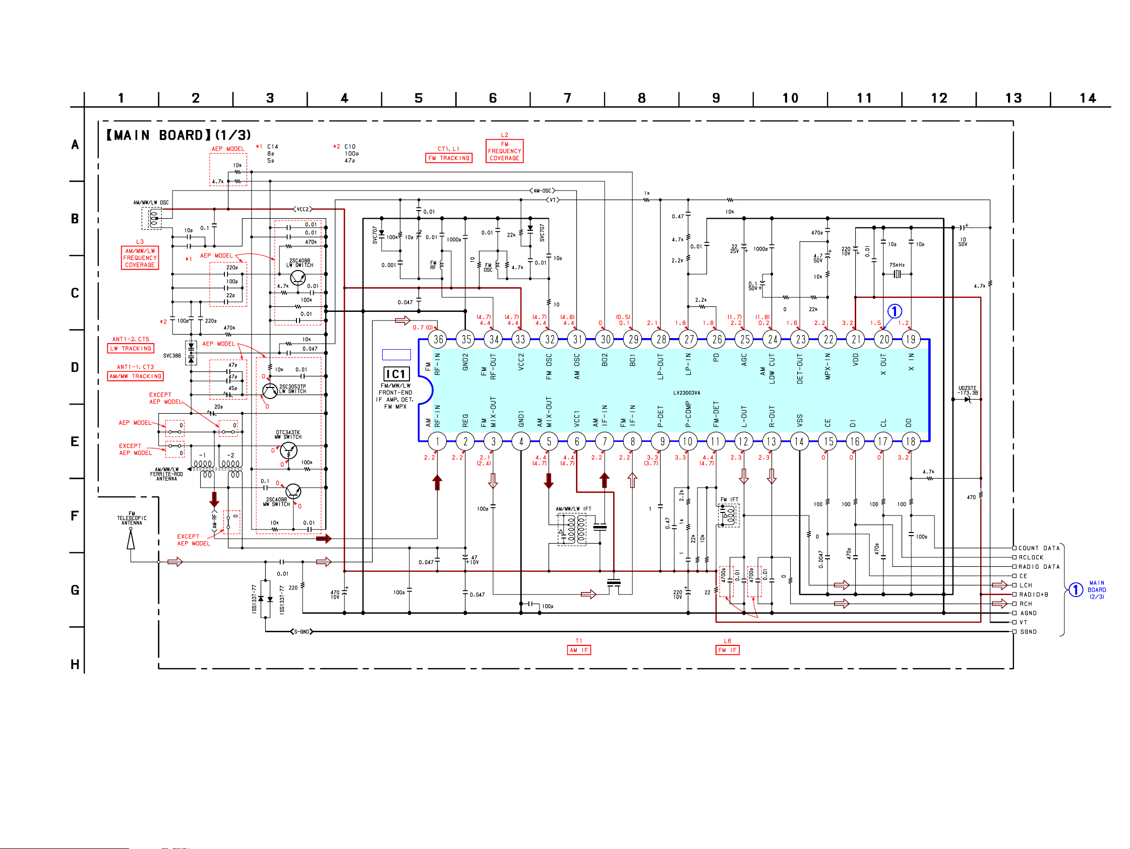
6-7. SCHEMA TIC DIAGRAM — MAIN SECTION (1/3) —
R30
R35
L3
C15
C13
C14
C63
C62
C61
C11
C10
D3
C12
R6
C54
C53
CT5
(CND,E92,MX)
(EXCEPT CND,E92,MX)
C69
C68
R37
Q33
R38
R34
C64
R36
C60
R5
C9
C55
Q35
• Refer to page 19 for W aveforms. • Refer to page 32 for IC Block Diagram.
(CND,E92,MX)
(EXCEPT CND,E92,MX)
R11
C2
C4
D1
R1 CT1
C1
C3
C67
L1
R7
C7
R2
L2
D2
C6
C5
R3
R4
IC B/D
C16
R9
R13
IC1
C45
R12
R14
C17
C19
C46
R39
R15
C20
C18
R27
C39
C40
C42C41
X1
C43
R24
D6
ANT2
JC2
JC1
ANT1
CT3
JC3
JC4
Q32
R32
C52
R29
R10
L6
C31
C32
C33
CND,E92,MX MODEL
C34
R18 R19 R20 R21
R16
C35
R17
C36
C37
Q31
C21
C51
C22
R26
D5
C29
C70
R31
D4
C23
C24
C25
C72
T1
CF3
CF2
C26
C27
R28
R25
R41
C28
C30
R22
R23
C38
(Page 24)
CFD-S03CP/S03CPL
23 23
CFD-S03CP/S03CPL
Ver. 1.4
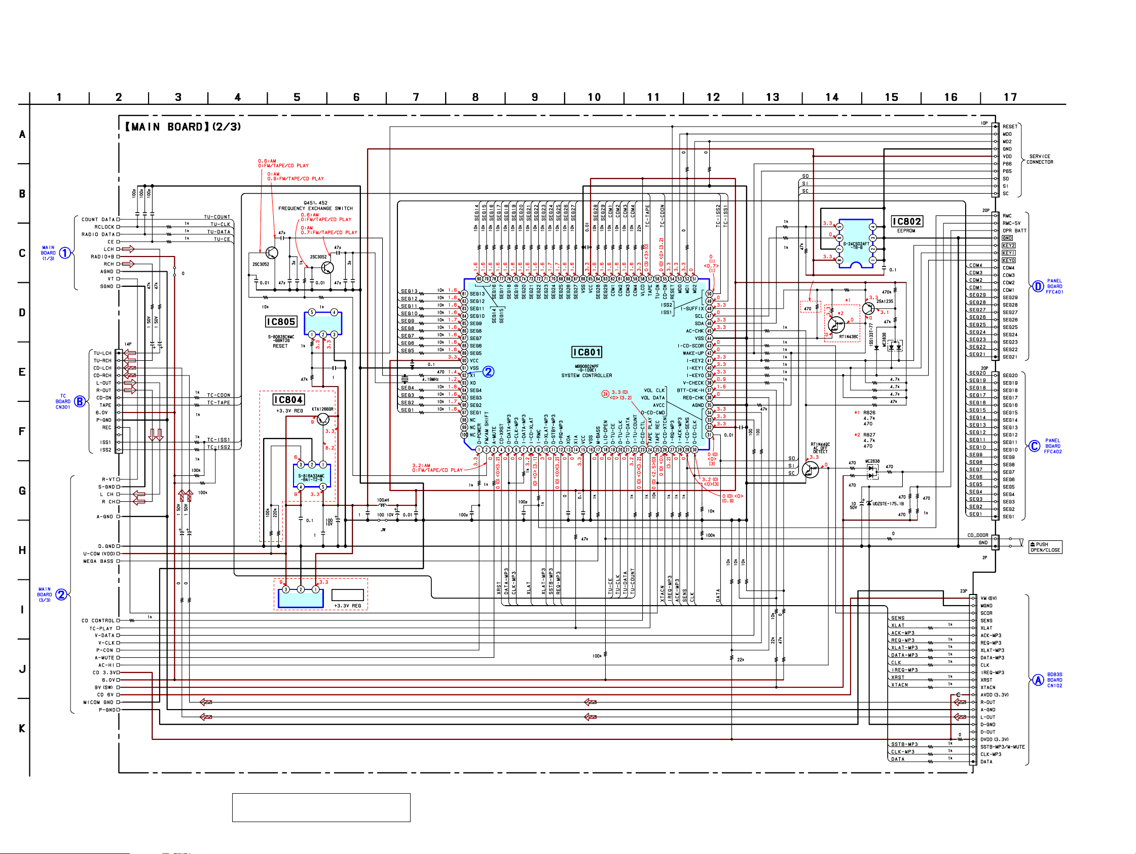
6-8. SCHEMATIC DIAGRAM — MAIN SECTION (2/3) —
C823
C822
C821
R817
R818
R819
(Page 23)
(Page 27)
FFC802
R261
C261
R161
C161
JC804
C162
R471
R472
R473
R474
R486
R487
C262
Q452
C458
R453
TYPE A
R883
• Refer to page 19 for Waveforms. • Refer to page 37 for IC Pin Description of IC801.
C456
R854
R853
R852
R851
R850
R849
R848
R847
Q451
R452
C452
R885
R886
IC804
C803
C457
R451
C806
Q802
C805
C804
C454 C453
IC805
R884
C455
C451
C825
L803
L804
C808
C807
X802
C819
R855
R856
R857
R858
R859
R860
R861
R862
R863
R868
R864
R865
R866
R867
C818
R801
R803
C816
R804
R846
R845
R805
R844
R843
R842
C811
R841
IC801
C813
R478
C815
R840
R831
R839
R838
R837
R836
R835
R809
R488
R810
R811
R812
R813
R492
R491
R814
R490
R479
R476
C814
R483
R815
R816
R802
R824
R482
R823
R822
R821
R825
R870
R869
R484
UK,E41,CET,IT,SP,TH MODEL
Q801
R826
R827
Q806
AEP,AUS,KR,
AR,TW MODEL
R898
R461
R462
C461
IC802
R820
Q805
R481
D802
D801
R830
R829
R828
R480
(AEP,AUS,KR,TW)
(CND,E92,MX,AR)
(AEP,AR)
(AUS,KR,TW)
D461
R463
D462
R493
C820
R464
R465
CN807
CN804
(Page 29)
CN803
(Page 29)
R466
R467
SW2
CN806
(Page 25)
CFD-S03CP/S03CPL
R475
R162
R262
TYPE B
IC806
XC6202P332FR
IC806
Refer to NOTE FOR REPLACEMENT OF THE
IC804 AND IC806 on page 4 for type A and B.
R894
R896
R893
CN805
R880
R879
R878
R877
R876
R875
R874
R873
R872
R871
FB832
(Page 21)
FB831
R477
R887
R889
R888
R892
R891
2424
CFD-S03CP/S03CPL
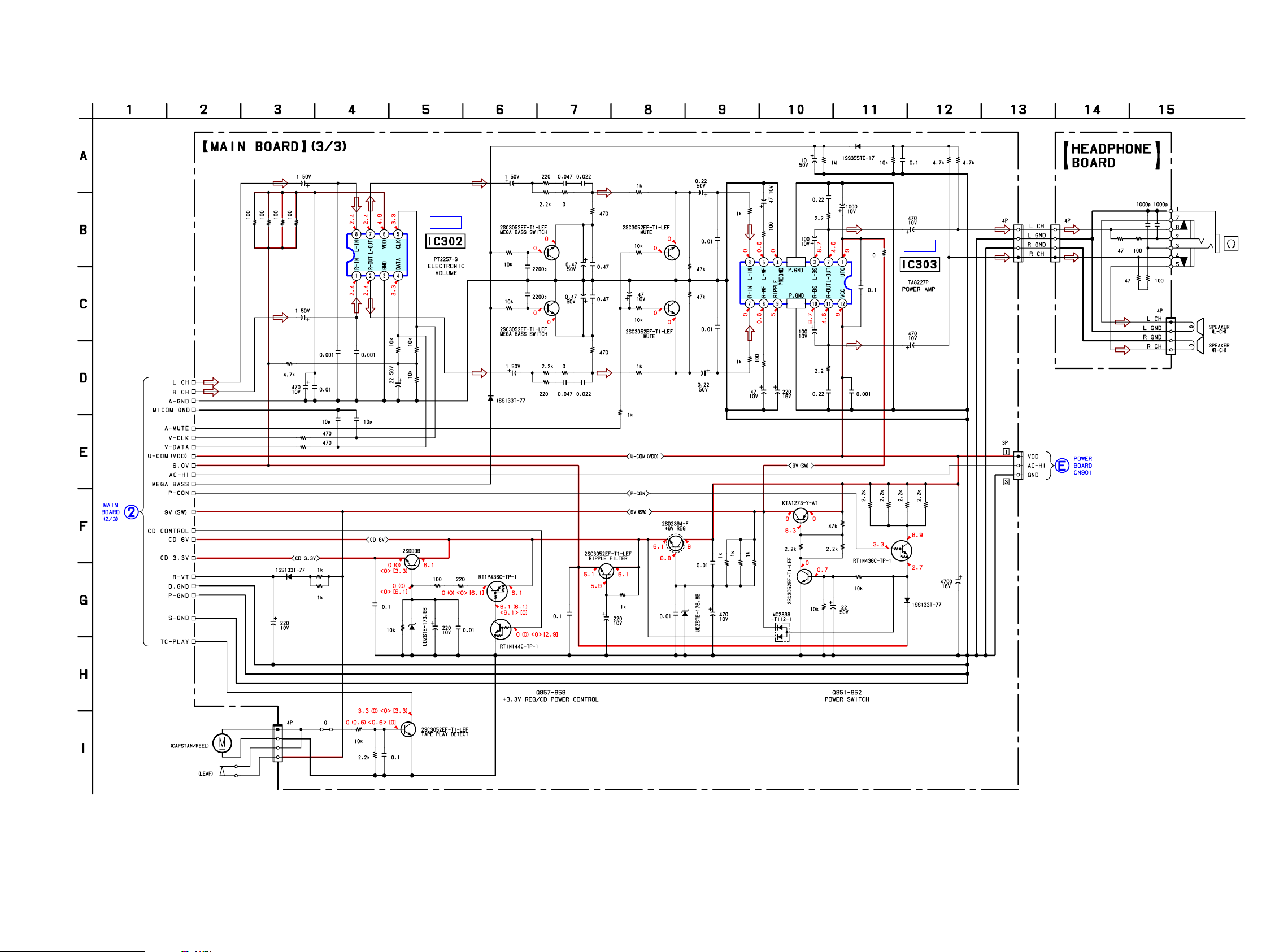
6-9. SCHEMATIC DIAGRAM — MAIN SECTION (3/3) —
C113
R330
R329
R328
R321
C213
C117
R335
C353
C330
C349
R332
R331
• Refer to page 32 for IC Block Diagrams.
C217
C350
R338
C311
R337
R336
IC B/D
IC302
C115
R139
R239
D322
R134
R135 R136
Q122
C106
C206
Q222
C215
R234
C129
R236R235
C229
C125
C225
C132
C232
R138
C127
C227
R238
R327
R140
R147
C331
R247
R240
Q124
Q224
C130
R141
R241
C230
C108
C208
R142
R242
C231
R243
C131
143
R
C322
C323
C119
C219
C110
R144
R244
C210
R323
C355
D323
C354
R316
C356
R324
C324
C112
IC B/D
IC303
C212
R245 R145
CN306
CN305
C216 C116
CN307
J321
R146R148
R246R248
CN308
SP101
SP201
(Page 24)
M901
SW1
C326
D324
CN304
R325
R326
JC807
R897
R899
C961
R965
C817
Q957
R959 R958
D957
C959
Q808
C957
Q958
Q959
C358
Q304
C357
R333
C952
Q955
C951
D953
C953
R960
R955
R954
D951
R952
Q953
Q952
R957
R951
R953
C956
R956
R961
Q951
R962
R963
(Page 31)
R964
C325
D952
CFD-S03CP/S03CPL
25 25
CFD-S03CP/S03CPL
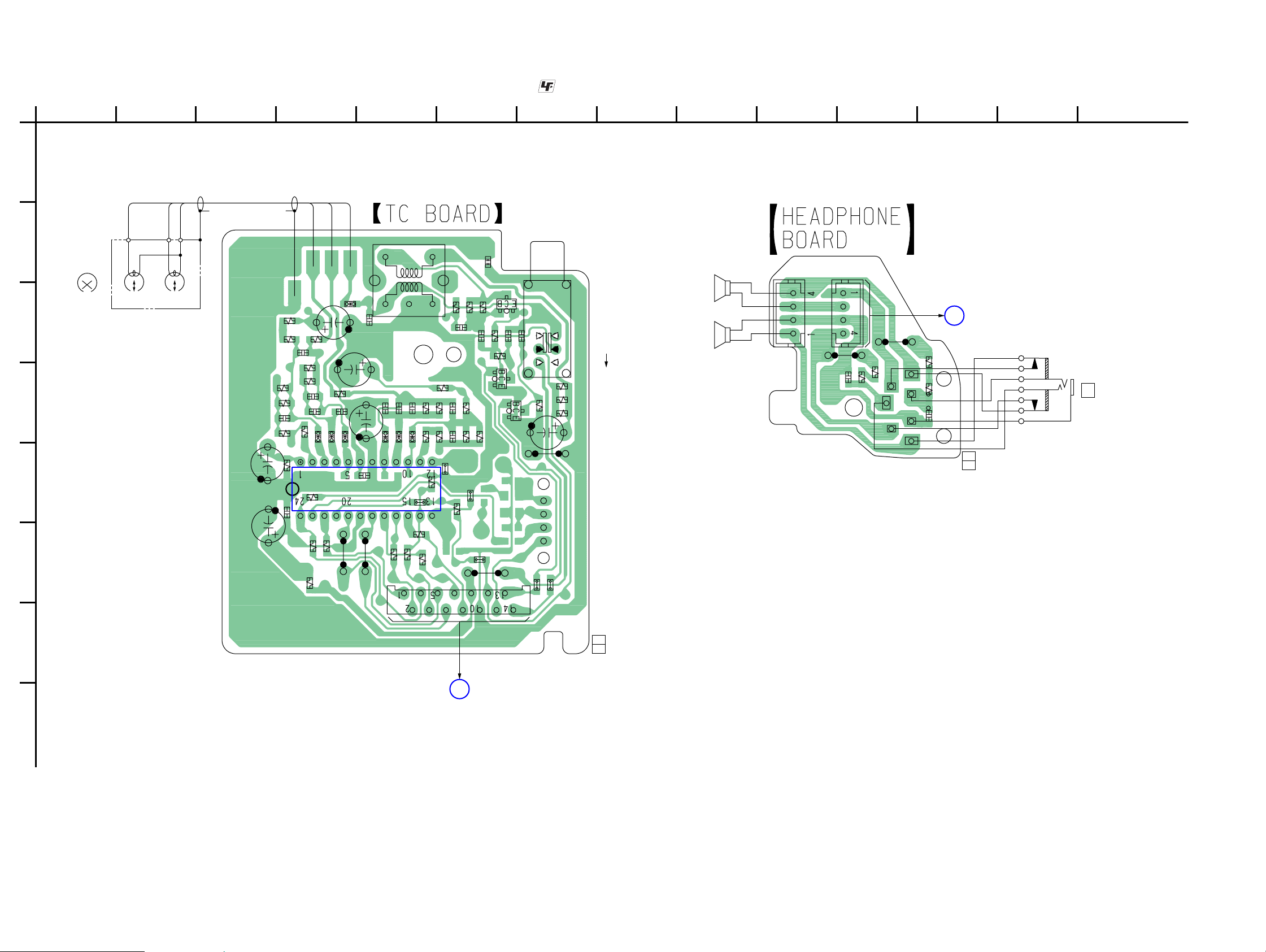
6-10. PRINTED WIRING BOARDS — TC SECTION —
1
234567891011 12 13 14
A
HT
W
RED
YEL
BLK
B
C
D
HE301
ERASE
HEAD
(L-CH)
RECORD/PLAYBACK
HRP300
HEAD
(R-CH)
R102
R108
C105
R109
R103
C103
R104
C301
E
C303
F
• Refer to page 19 for Circuit Boards Location. : Uses unleaded solder.
HT
RED
FB201
R105
C102
FB202
R111
C104
JW301
YEL
FB207
C202
R210
FB203
C309
IC301
302
JW
C305
C302
C204
FB204
R211
T301
C201
FB205
JC305
R205
R302
C207
FB206
R206
C306
R202
R201
R212
R303
R207
R204
JC302
R304
CN301
R308
C205
C203
R312
C307
R208
R203
JC303
JC306
JW
R306
R209
303
R307
C318
Q301
C310
Q303
R310
C308
Q302
S301
R311
C304
JW
304
R314
R305
R315
S301
(REC/PB)
PB
REC
BLK
R107
R101
C312
W
R110
C107
C101
R112
R301
R106
R309
SP201
SPEAKER
(R-CH)
SP101
SPEAKER
(L-CH)
CN308
JW321
CN307
C116
R146
JW322
R148
R248
R246
C216
1-869-164-
F
MAIN BOARD
CN306
(Page 22)
11
(11)
5
4
3
2
6
7
1
J321
i
G
H
CFD-S03CP/S03CPL
B
MAIN BOARD
FFC802
(Page 22)
1-869-165-
JC307
JC308
(11)
11
2626
CFD-S03CP/S03CPL
Ver. 1.2
6-11. SCHEMATIC DIAGRAM — TC SECTION —
HRP301
HE301
S301
• Refer to page 19 for Waveforms. • Refer to page 33 for IC Block Diagram.
C301
FB207
C102 R102 R108
R301
R110
R210
C309
C104
C101
C107
R101
R107
R207
R201
C207
C201
C204
R202 R208C202
(AEP,UK,CET,KR,IT)
(CND,E41,E92,AUS,MX,SP,AR,TH,TW)
R103
R112
FB202
FB203
FB204
FB205
FB206
R104
FB201
R204
JC302
R212
R109
C103
C105
C302
C205
C203
R209
R203
IC301
R106
R206
JC303
IC B/D
R111
C312
JC305
R303
R211
R302
R309
R205
C303
R304
JC306
CN301
R105
C318
R310
C310
Q302 Q303
R311
C308
C305
R308
T301
C306
C304
FFC802
(Page 24)
R314R305
R315
R312R306
Q301
JC308 JC307
C307
R307
CFD-S03CP/S03CPL
27 27
CFD-S03CP/S03CPL
Ver. 1.1
6-12. PRINTED WIRING BOARDS — PANEL SECTION —
1
234567891011 12 13 14
A
B
C
D
S416
/
TUNE
S415
/
TUNE
R417
R416
S415
S416
R418
R415
S417
x
S417
R419
S414
S414
>/PRESET
R411
R412
R413
R414
S407
BX
S407
R409
S413
S413
./PRESET
• Refer to page 19 for Circuit Boards Location. : Uses unleaded solder.
R408
S406
S406
REPEAT
R407
(Page 22) (Page 22)
MAIN BOARD
CN804
D
FFC401
LIQUID CRYSTAL DISPLAY UNIT
LCD401
MAIN BOARD
CN803
C
FFC4021
IC401
IC401
123
C401
D406
R430
1-869-161-
D406
OPR/BATT
R432
SLEEPMODE
401
20120
133
S405
R406
S404
S404
DISPLAY/
ENTER
R405
S402
R403
R404
S403
S403
MEGA BASS
R402
R401
(EXCEPT AEP,UK,CET,IT)
(AEP,UK,CET,IT)
JW
S401
S401
z/POWER
z/OPERATE
R431
(11)
11
CN403
24
13
E
F
G
H
3
1
2
4
R422
CN421
S424
R424
VOLUM
R423
S422
TAPE
S423
1-849-163-
E
(11)
11
FFC412
R421
S421
RADIO/BAND/
AUTO PRESET
FFC411
S411
CD
1-869-162-
11
(11)
I
CFD-S03CP/S03CPL
2828
6-13. SCHEMATIC DIAGRAM — PANEL SECTION —
R401 R402 R403 R404 R405 R406 R407 R408 R409
CFD-S03CP/S03CPL
Ver. 1.1
(EXCEPT AEP,UK,CET,IT)
OPERATE
(AEP,UK,CET,IT)
S403S402S401
R411 R412 R413 R414 R415 R416 R417 R418 R419
LCD401
S404
S414S413
S405
S415
S406 S407
S416
R430
C401
S417
IC401
D406
CN403 FFC411
RADIO/
BAND/
AUTO
PRESET
R421
S422S421S411
R422 R423
FFC412 CN421
S424S423
R424
FFC422
R432 R431
FFC402 FFC401
(Page 24)
(Page 24)
CFD-S03CP/S03CPL
29 29
CFD-S03CP/S03CPL
6-14. PRINTED WIRING BOARDS — POWER SUPPLY SECTION —
1
234567891011 12 13 14
A
B
T901
FH901 FH902
C903
C
C902
D
• Refer to page 19 for Circuit Boards Location. : Uses unleaded solder.
F902
D903
C901
D901
D902
D904
C904
907
JW
JW908
C906
CN902
CN901
GRY
RED
E
MAIN BOARD
CN305
(Page 22)
CN903
905
JW
904
JW
1-869-167-
11
(11)
E
F
G
H
J901
–
+
AC IN
-
1-869-166-
(11)
11
JW901
JW900
+
DRY BATTERY
(IEC DESIGNATION R20)
–
SIZE "D"
6pcs, 9V
–
+
JW902
JW903
1-869-168-
(11)
11
I
CFD-S03CP/S03CPL
3030
 Loading...