

Page 1
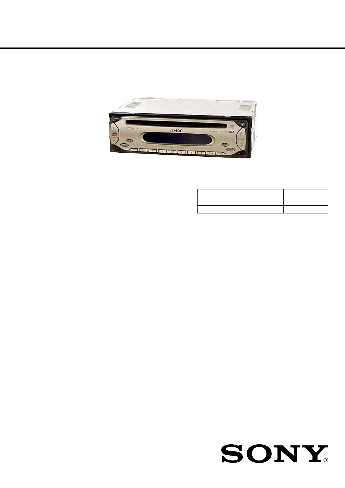
CDX-S2000/S2000S/SW200
SERVICE MANUAL
Ver 1.0 2003. 11
• The tuner and CD sections have no adjustments.
AUDIO POWER SPECIFICATIONS (US Model)
POWER OUTPUT AND TOTAL HARMONIC DISTORTION
23.2 watts per channel minimum continuous average power into
4 ohms, 4 channels driven from 20 Hz to 20 kHz with no more
than 5% total harmonic distortion.
SPECIFICATIONS
CD player section
Signal-to-noise ratio 120 dB
Frequency response 10 – 20,000 Hz
Wow and flutter Below measurable limit
Tuner section
FM
Tuning range US, Canadian Model:
87.5 – 107.9 MHz
E model:
FM tuning interval:
50 kHz/200 kHz
switchable
87.5 – 108 MHz (at 50 kHz step)
87.5 – 107.9 MHz (at 200 kHz step)
Antenna terminal External antenna connector
Intermediate frequency 10.7 MHz/450 kHz
Usable sensitivity 9 dBf
Selectivity 75 dB at 400 kHz
Signal-to-noise ratio 67 dB (stereo),
69 dB (mono)
Harmonic distortion at 1 kHz
0.5% (stereo),
0.3% (mono)
Separation 35 dB at 1 kHz
Frequency response 30 – 15,000 Hz
US Model
CDX-S2000/SW200
Canadian Model
CDX-S2000
E Model
CDX-S2000/S2000S
Model Name Using Similar Mechanism NEW
CD Drive Mechanism Type MG-611XA-186//K
Optical Pick-up Name KSS1000E
AM
Tuning range US, Canadian Model:
530 – 1,710 kHz
E Model:
AM tuning interval:
9 kHz/10 kHz switchable
531 – 1,602 kHz (at 9 kHz step)
530 – 1,710 kHz (at 10 kHz step)
Antenna terminal External antenna connector
Intermediate frequency 10.7 MHz/450 kHz
Sensitivity 30 µV
Power amplifier section
Outputs Speaker outputs
(sure seal connectors)
Speaker impedance 4 – 8 ohms
Maximum power output 52 W × 4 (at 4 ohms)
General
Outputs Audio outputs terminal (rear)
Power antenna relay control terminal
Power amplifier control terminal
Inputs Antenna input terminal
Tone controls Low: ±10 dB at 60 Hz (XPLOD)
Mid: ±10 dB at 1 kHz (XPLOD)
High: ±10 dB at 10 kHz (XPLOD)
9-961-387-01
2003K04-1
© 2003. 11
– Continued on next page –
FM/AM COMPACT DISC PLAYER
Sony Corporation
e Vehicle Company
Published by Sony Engineering Corporation
1
Page 2
CDX-S2000/S2000S/SW200
Power requirements 12 V DC car battery
(negative ground)
Dimensions Approx. 178 × 50 × 176 mm
(7 1/8 × 2 × 7 in.) (w/h/d)
Mounting dimensions Approx. 182 × 53 × 161 mm
(7 1/4 × 2 1/8 × 6 3/8 in.) (w/h/d)
Mass Approx. 1.2 kg
(2 lb. 10 oz.)
Supplied accessories Parts for installation and connections (1 set)
Front panel case (1)
Design and specifications are subject to change without
notice.
SERVICE NOTES
NOTES ON HANDLING THE OPTICAL PICK-UP BLOCK
OR BASE UNIT
The laser diode in the optical pick-up block may suffer electrostatic
breakdown because of the potential difference generated by the
charged electrostatic load, etc. on clothing and the human body.
During repair, pay attention to electrostatic breakdown and also use
the procedure in the printed matter which is included in the repair
parts.
The flexible board is easily damaged and should be handled with
care.
CAUTION
Use of controls or adjustments or performance of procedures
other than those specified herein may result in hazardous
radiation exposure.
If the optical pick-up block is defective, please replace the whole
optical pick-up block.
Never turn the semi-fixed resistor located at the side of optical
pick-up block.
optical pick-up
semi-fixed resistor
NOTES ON LASER DIODE EMISSION CHECK
The laser beam on this model is concentrated so as to be focused on
the disc reflective surface by the objective lens in the optical pickup block. Therefore, when checking the laser diode emission, observe from more than 30 cm away from the objective lens.
Notes on Chip Component Replacement
• Never reuse a disconnected chip component.
• Notice that the minus side of a tantalum capacitor may be dam-
aged by heat.
TEST DISCS
This set can playback CD-R and CD-ROM discs. The following
test discs should be used to check the capability:
CD-R test disc TCD-R082LMT (Part No. J-2502-063-1)
CD-RW test disc TCD-W082L (Part No. J-2502-063-2)
• E model
This label is located on the bottom of the chassis.
SAFETY-RELATED COMPONENT WARNING!!
COMPONENTS IDENTIFIED BY MARK 0 OR DOTTED LINE
WITH MARK 0 ON THE SCHEMATIC DIAGRAMS AND IN
THE PARTS LIST ARE CRITICAL TO SAFE OPERATION.
REPLACE THESE COMPONENTS WITH SONY P ARTS WHOSE
PART NUMBERS APPEAR AS SHOWN IN THIS MANUAL OR
IN SUPPLEMENTS PUBLISHED BY SONY.
2
ATTENTION AU COMPOSANT AYANT RAPPORT
À LA SÉCURITÉ!!
LES COMPOSANTS IDENTIFIÉS P AR UNE MARQUE 0 SUR LES
DIAGRAMMES SCHÉMATIQUES ET LA LISTE DES PIÈCES
SONT CRITIQUES POUR LA SÉCURITÉ DE FONCTIONNEMENT.
NE REMPLACER CES COMPOSANTS QUE PAR DES PIÈCES
SONY DONT LES NUMÉROS SONT DONNÉS DANS CE MANUEL
OU DANS LES SUPPLÉMENTS PUBLIÉS PAR SONY.
Page 3
CDX-S2000/S2000S/SW200
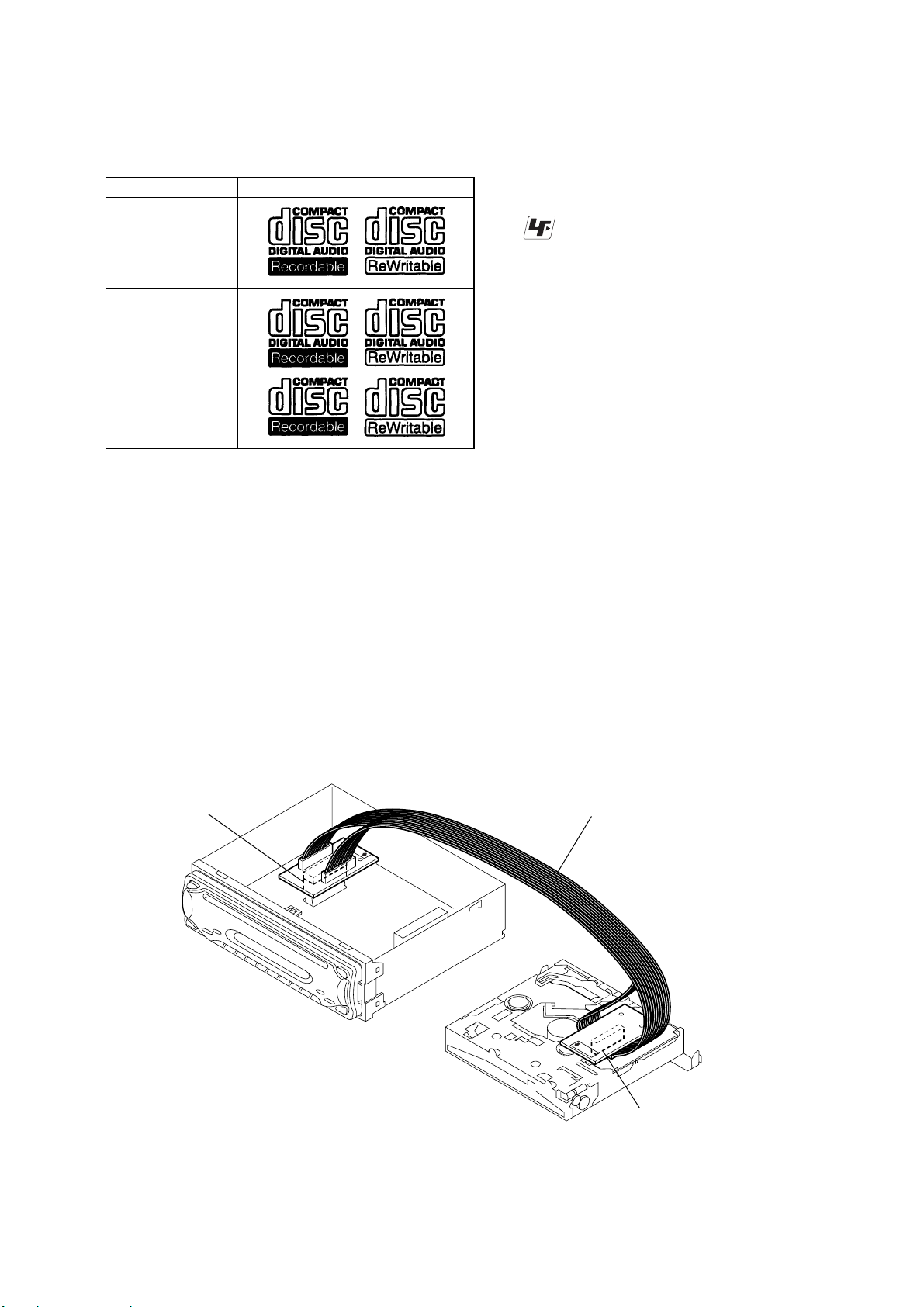
D
Notes on CD-Rs (recordable CDs)/CD-RWs (rewritable
CDs)
This unit can play the following discs:
Type of discs Label on the disc
Audio CD
MP3 files
• Some CD-Rs/CD-RWs (depending on the equipment used for
its recording or the condition of the disc) may not play on this
unit.
• You cannot play a CD-R/CD-RW that is not finalized∗.
• You can play MP3 files recorded on CD-ROMs, CD-Rs, and
CD-RWs.
• A CD-R/CD-RW to which a session can be added can be played.
z
UNLEADED SOLDER
Boards requiring use of unleaded solder are printed with the lead
free mark (LF) indicating the solder contains no lead.
(Caution: Some printed circuit boards may not come printed with
the lead free mark due to their particular size.)
: LEAD FREE MARK
Unleaded solder has the following characteristics.
• Unleaded solder melts at a temperature about 40°C higher than
ordinary solder.
Ordinary soldering irons can be used but the iron tip has to be
applied to the solder joint for a slightly longer time.
Soldering irons using a temperature regulator should be set to
about 350°C.
Caution: The printed pattern (copper foil) may peel away if the
heated tip is applied for too long, so be careful!
• Strong viscosity
Unleaded solder is more viscous (sticky, less prone to flow)
than ordinary solder so use caution not to let solder bridges
occur such as on IC pins, etc.
• Usable with ordinary solder
It is best to use only unleaded solder but unleaded solder may
also be added to ordinary solder.
∗ A process necessary for a recorded CD-R/CD-RW disc to be
played on the audio CD player.
EXTENSION CABLE AND SERVICE POSITION
When repairing or servicing this set, connect the jig (extension cable)
as shown below.
• Connect the MAIN board (CN751) and the SERVO board (CN1)
with the extension cable (Part No. J-2502-076-1).
MAIN BOARD
CN751
J-2502-076-1
SERVO BOAR
CN1
3
Page 4

CDX-S2000/S2000S/SW200
1. GENERAL
Location of Controls (US, Canadian Model) .......................... 5
Location of Controls (E Model) .............................................. 5
Connections (US, Canadian Model)........................................ 6
Connections (E Model) ........................................................... 7
2. DISASSEMBLY
2-1. Sub Panel (1) Assy .............................................................. 9
2-2. CD Mechanism Block ......................................................... 9
2-3. Main Board ....................................................................... 10
2-4. Chassis (T) Sub Assy ........................................................ 10
2-5. Roller Arm Assy ................................................................ 11
2-6. Chassis (OP) Assy.............................................................11
2-7. Optical Pick-up ................................................................. 12
2-8. SL Motor Assy (M902) .....................................................12
2-9. LE Motor Assy (M903)..................................................... 13
2-10. Servo Board....................................................................... 13
3. DIAGRAMS
3-1. IC Pin Descriptions ........................................................... 14
3-2. Block Diagram –CD Section–........................................... 18
3-3. Block Diagram –Main Section–........................................19
3-4. Block Diagram –Display Section–....................................20
3-5. Circuit Boards Location .................................................... 20
3-6. Note for Printed Wiring Boards and
Schematic Diagrams ..........................................................21
3-7. Waveforms......................................................................... 21
3-8. Printed Wiring Boards –CD Mechanism Section–............ 22
3-9. Schematic Diagram –CD Mechanism Section– ................23
3-10. Schematic Diagram –Main Section (1/2)– ........................24
3-11. Schematic Diagram –Main Section (2/2)– ........................25
3-12. Printed Wiring Boards –Main Section– ............................ 26
3-13. Printed Wiring Board –Display Section– .......................... 27
3-14. Schematic Diagram –Display Section–............................. 28
3-15. IC Block Diagrams............................................................ 29
TABLE OF CONTENTS
4. EXPLODED VIEWS
4-1. Main Section ..................................................................... 31
4-2. Front Panel Section ........................................................... 32
4-3. CD Mechanism Section (1) ...............................................33
4-4. CD Mechanism Section (2) ...............................................34
4-5. CD Mechanism Section (3) ...............................................35
4-6. CD Mechanism Section (4) ...............................................36
5. ELECTRICAL PARTS LIST ........................................ 37
4
Page 5
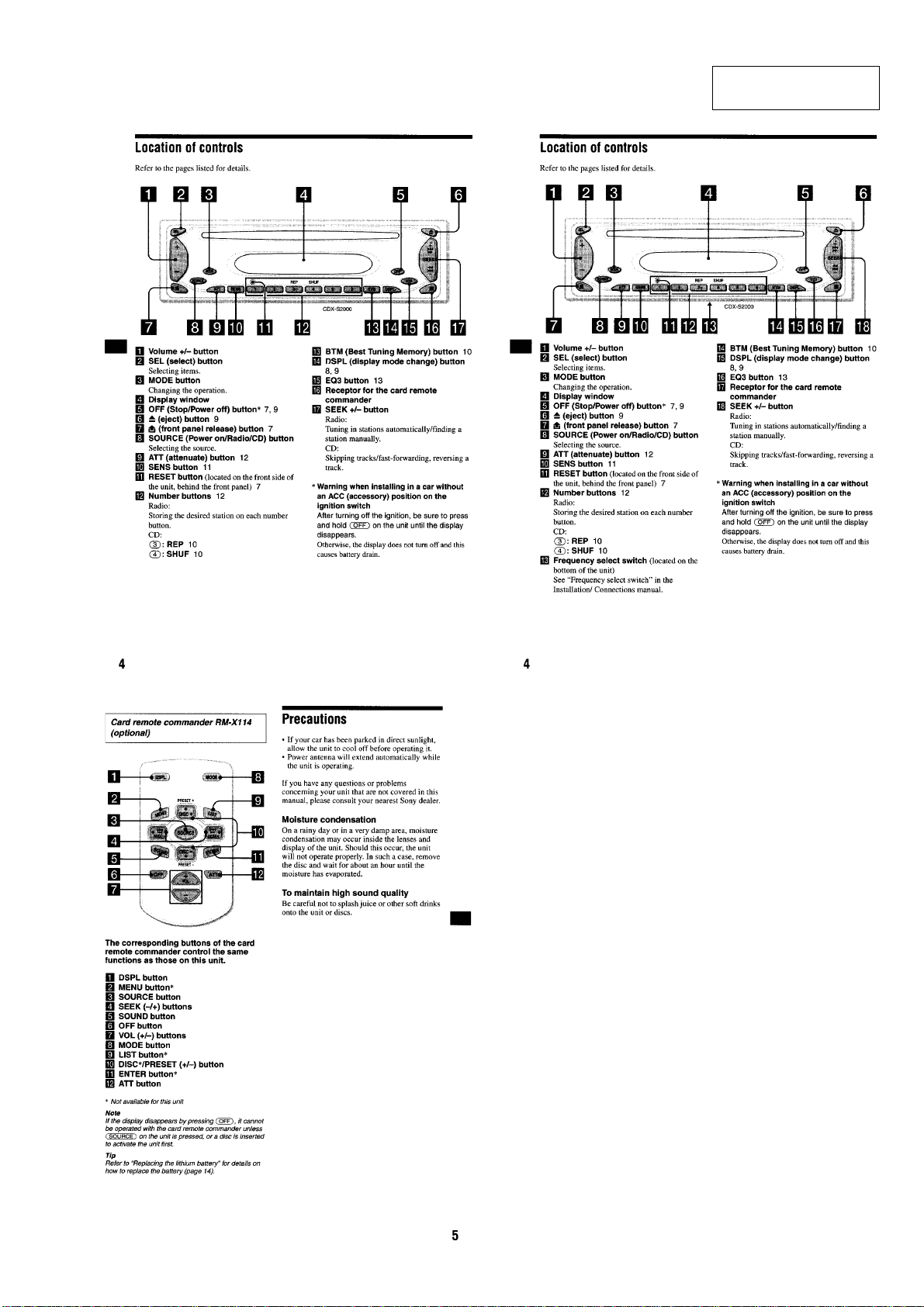
CDX-S2000/S2000S/SW200
SECTION 1
GENERAL
(US, Canadian Model) (E Model)
This section is extracted
from instruction manual.
5
Page 6
CDX-S2000/S2000S/SW200
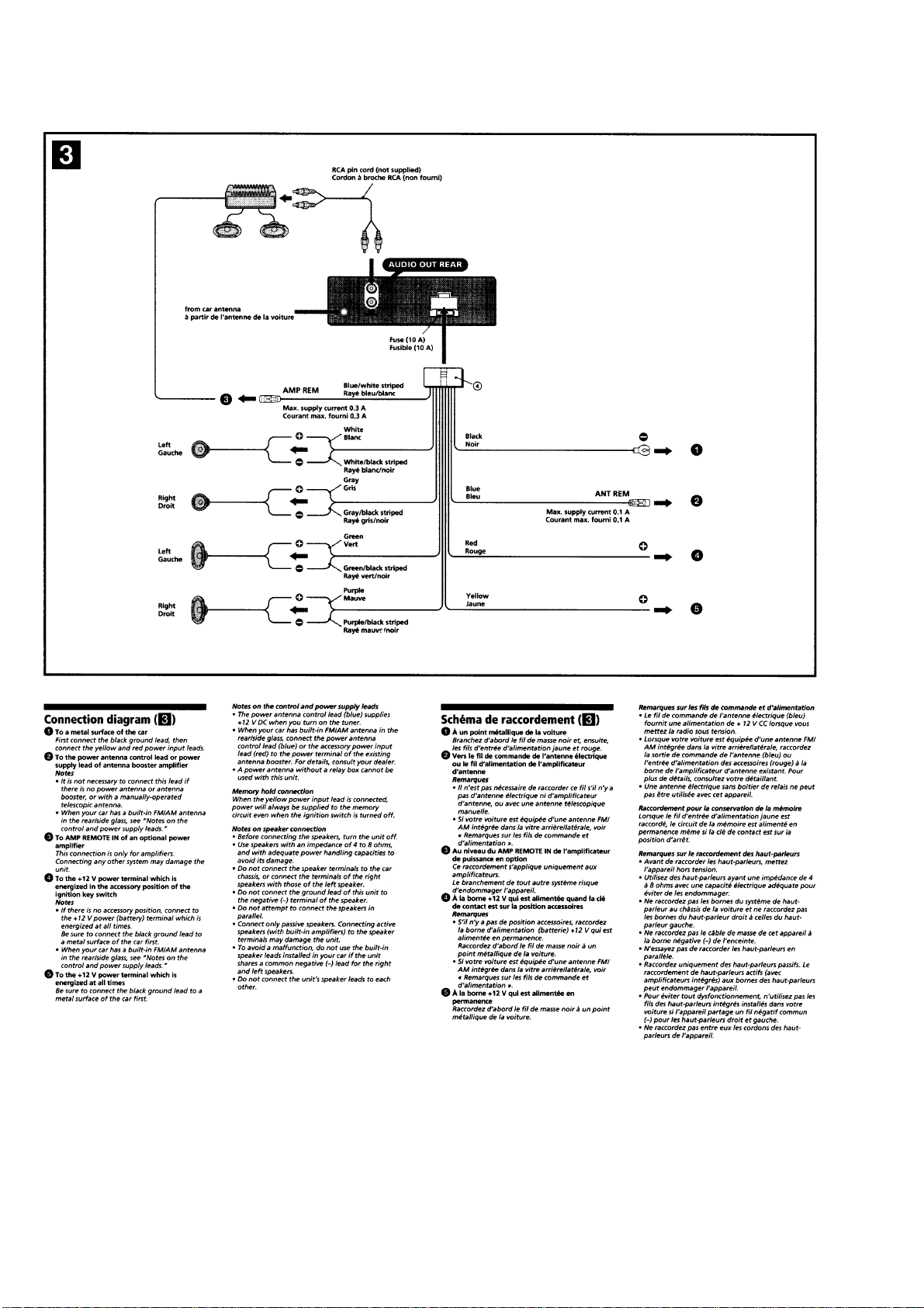
Connections (US, Canadian Model)
6
Page 7
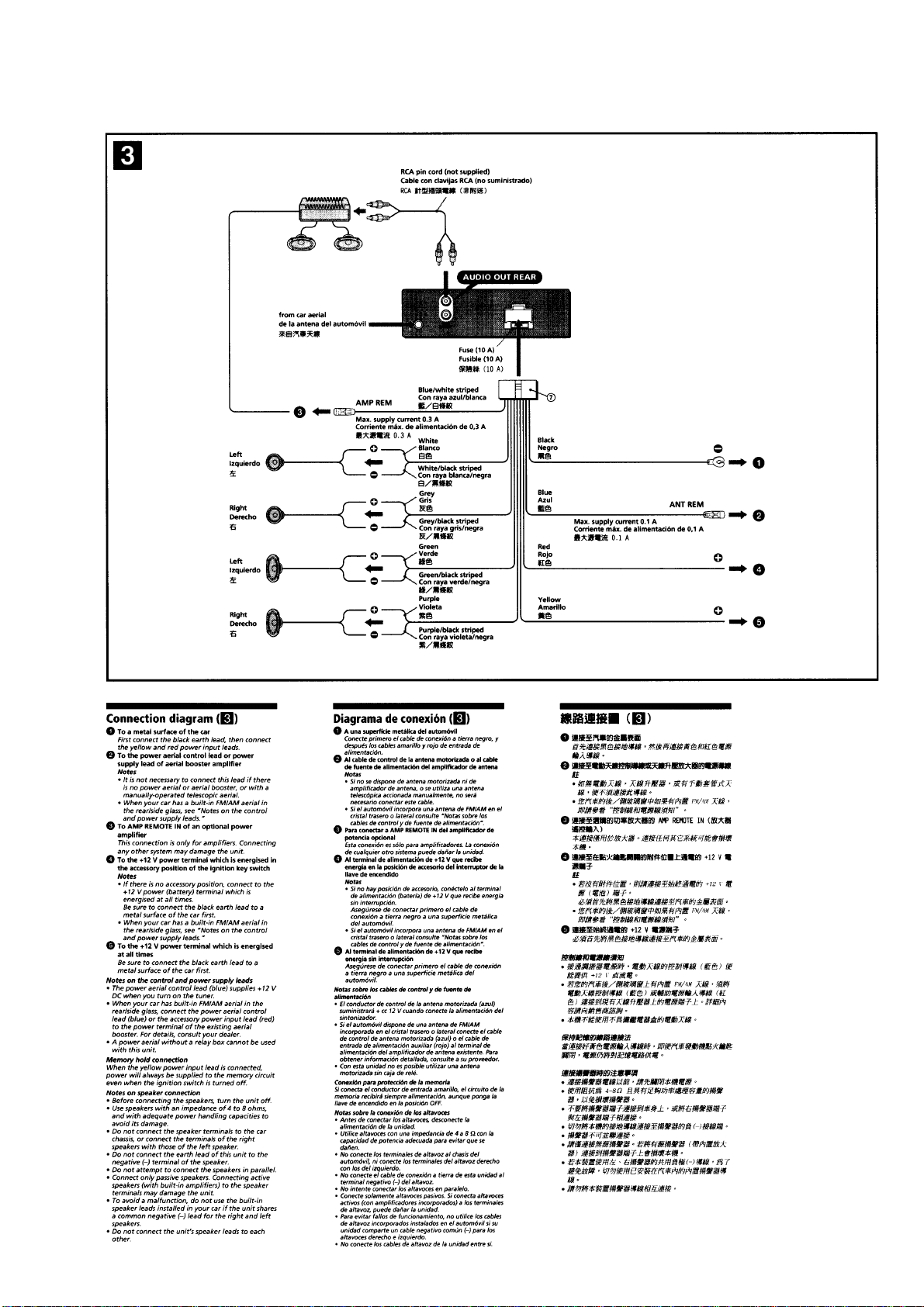
Connections (E Model)
CDX-S2000/S2000S/SW200
7
Page 8
CDX-S2000/S2000S/SW200
SECTION 2
DISASSEMBLY
Note : This set can be disassemble according to the following sequence.
SET
2-1. SUB PANEL (1) ASSY
(Page 9)
2-2. CD MECHANISM BLOCK
(Page 9)
2-3. MAIN BOARD
(Page 10)
2-7. OPTICAL PICK-UP
(Page 12)
2-4. CHASSIS (T) SUB ASSY
(Page 10)
2-5. ROLLER ARM ASSY
(Page 11)
2-6. CHASSIS (OP) ASSY
(Page 11)
2-8. SL MOTOR ASSY (M902)
(Page 12)
2-10. SERVO BOARD
(Page 13)
2-9. LE MOTOR ASSY (M903)
(Page 13)
8
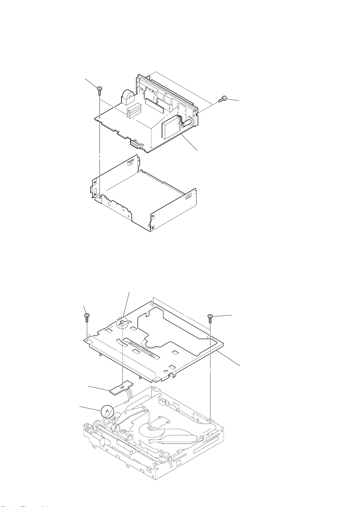
Page 9
Note : Follow the disassembly procedure in the numerical order given.
s
)
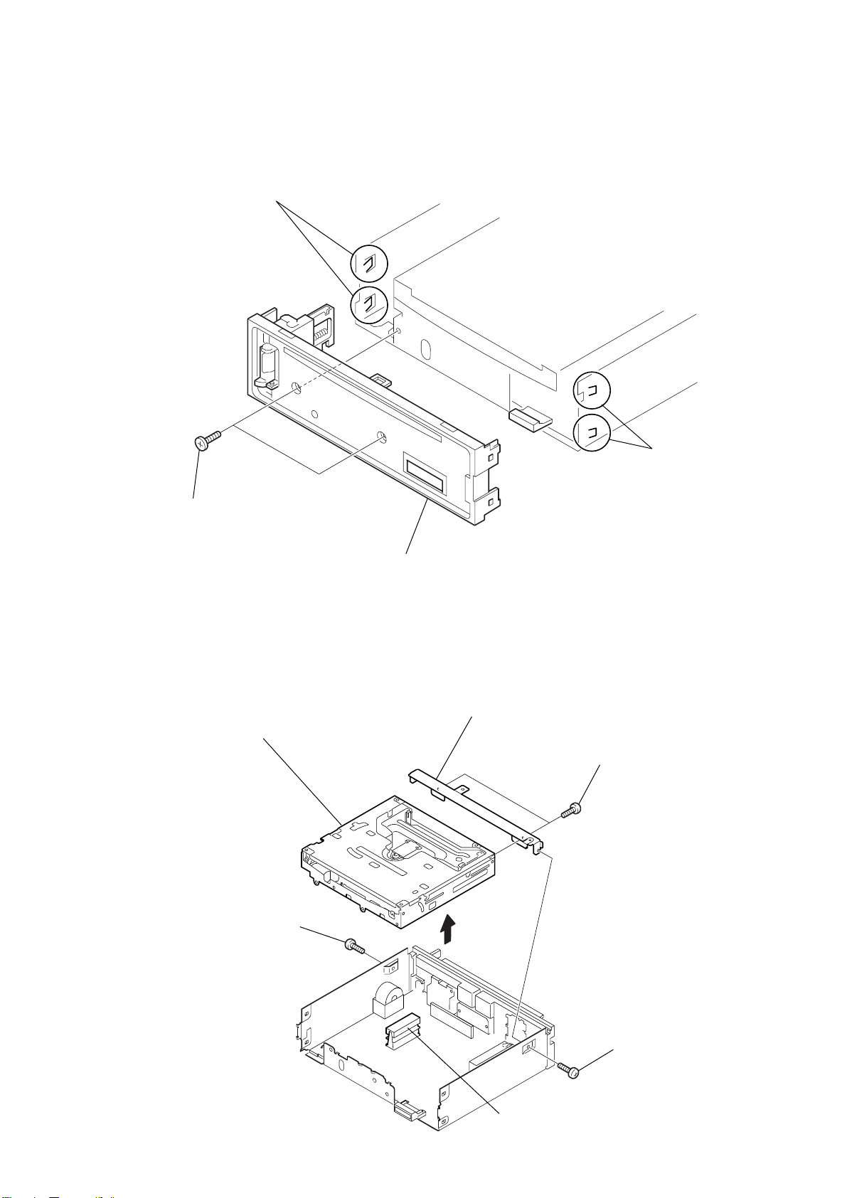
2-1. SUB PANEL (1) ASSY
3
two claws
CDX-S2000/S2000S/SW200
1
two
screws
(+PTT 2.6
x
6)
2-2. CD MECHANISM BLOCK
5
CD mechanism block
4
sub panel (1) assy
7
bracket (CD)
2
6
two
screws
(+PTT 2.6
two claw
x
6)
2
screw
(+PTT 2.6
x
6)
3
4
CN751
1
screw
(+PTT 2.6
x
6
9
Page 10
CDX-S2000/S2000S/SW200
)
2-3. MAIN BOARD
1
three screws
(+BTT)
3
MAIN board
2
two
screws
(+PTT 2.6
x
8
2-4. CHASSIS (T) SUB ASSY
2
two
screws
(+P 1.7
5
SENSOR board
3
claw
x
2.2)
4
claw
1
two
screws
x
(+P 1.7
6
2.2)
chassis (T) sub assy
10
Page 11
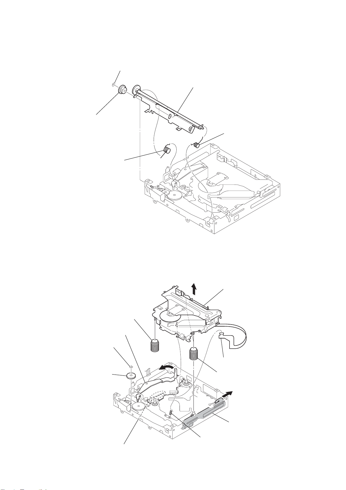
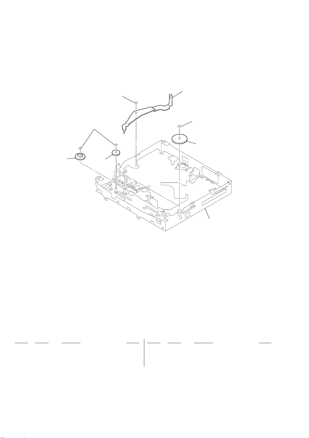
2-5. ROLLER ARM ASSY
)
4
worm wheel (RA)
1
spring (RAL)
3
washer (1.0 – 2.5)
5
roller arm assy
CDX-S2000/S2000S/SW200
2
spring (RAR)
2-6. CHASSIS (OP) ASSY
0
compression spring (damper)
4
washer
5
gear (LE1)
lever (D)
6
8
qa
chassis (OP) assy
1
CN2
9
two compression springs (damper
7
slider (R)
2
Remove the six solderings.
3
tension coil spring (KF)
11
Page 12
CDX-S2000/S2000S/SW200
2-7. OPTICAL PICK-UP
5
claw
2
chucking arm sub assy
1
tension coil spring (CHKG)
7
optical pick-up
2-8. SL MOTOR ASSY (M902)
6
main shaft
4
rack (SL)
3
screw
(+B 1.4
x
5)
12
2
SL motor assy (M902)
1
screw
(+P 1.4
x
1.8)
Page 13
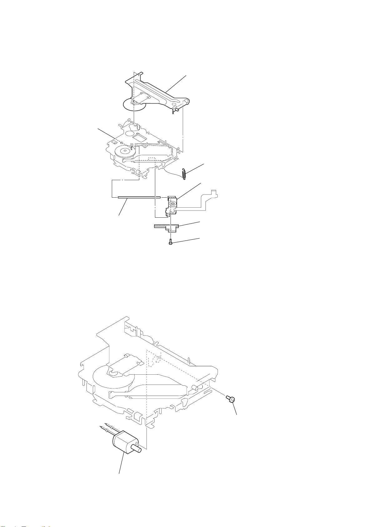
2-9. LE MOTOR ASSY (M903)
qf
two toothed lock
(+M 1.4
bracket (LEM)
qs
screw
(+M 1.7
x
)
screws
2.5)
6
screw
(+P 1.7
x
qd
2.2)
qa
screw
(+M 1.7
qg
(M903)
0
woam (LEB) assy
x
2.5)
LE motor assy
7
leaf spring (LE)
8
screw
(+M 1.7
9
bearing (LEB)
2
washer
gear (LE1)
3
lever (D)
CDX-S2000/S2000S/SW200
x
2.5)
4
slider (R)
5
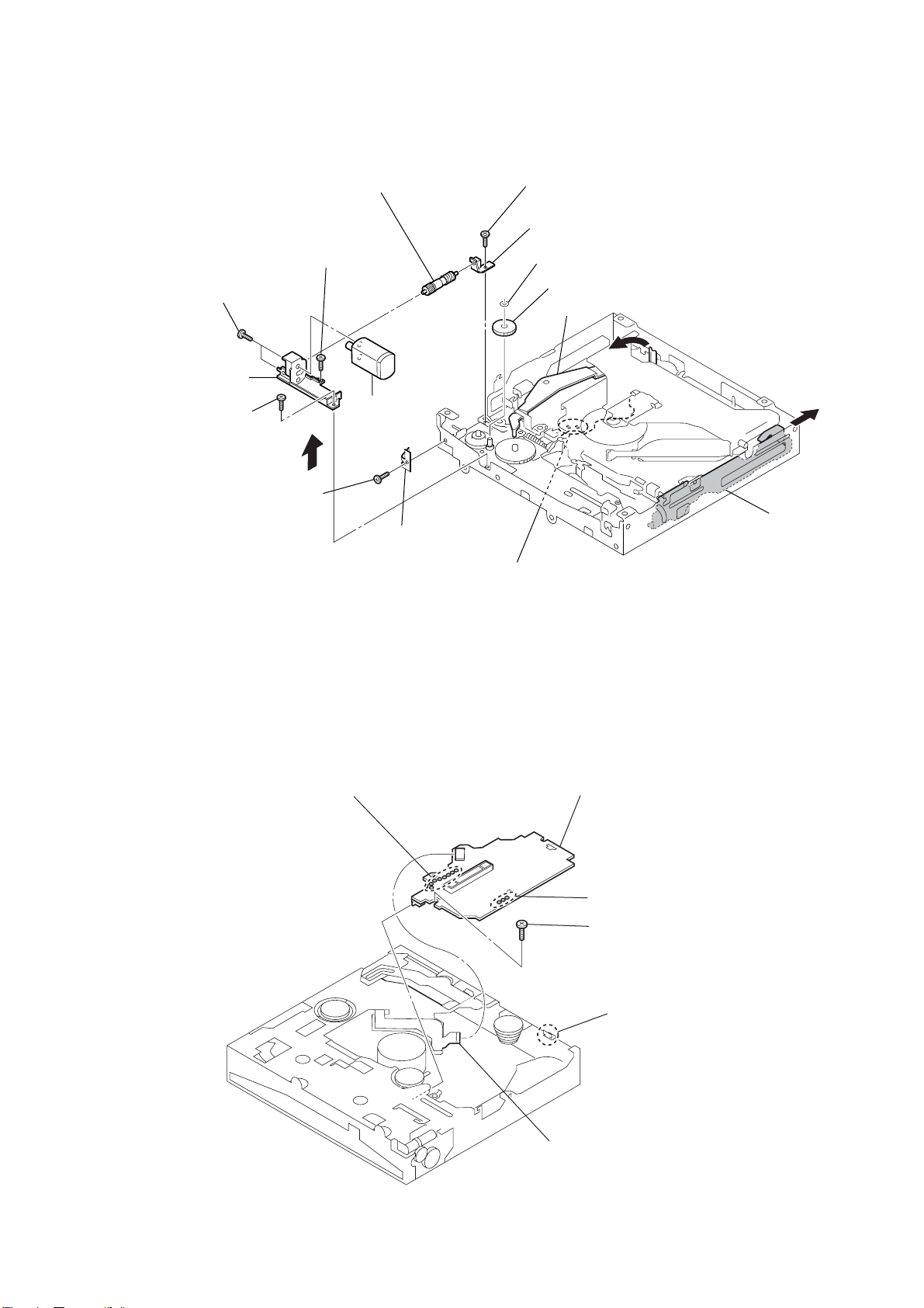
2-10. SERVO BOARD
1
Remove the eight solderings.
1
Remove the soldering.
6
SERVO board
2
Remove the three solderings.
4
toothed lock
(M 1.7)
5
screw
claw
3
CN2
13
Page 14

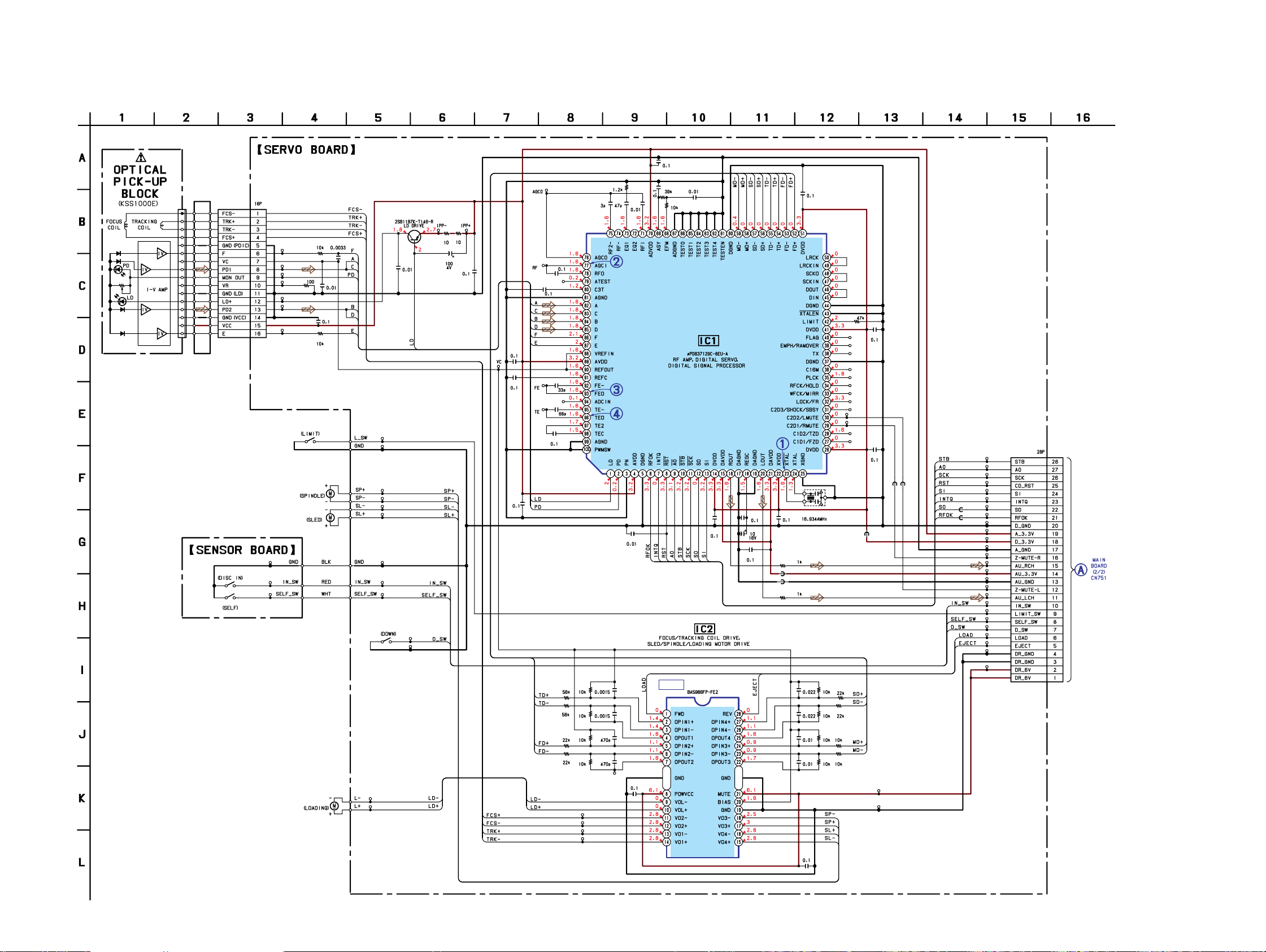
CDX-S2000/S2000S/SW200
SECTION 3
DIAGRAMS
3-1. IC PIN DESCRIPTIONS
• IC1 µPD63712GC-8EU-A (RF AMP, DIGITAL SERVO, DIGITAL SIGNAL PROCESSOR) (SERVO BOARD)
Pin No. Pin Name I/O Pin Description
1LDOLaser diode ON/OFF control signal output (L: laser OFF, H: laser ON)
2PDIDimmer monitor input from optical pick-up laser diode.
3PNINot used. (Fixed at L in this set)
4AVDD — Analog power supply pin (+3.3 V)
5 DGND — Ground
6 RFOK O RFOK signal output to system control IC.
7 INTQ O CD text pack synchronization signal output to system control IC.
8 RST I CD reset signal input from system control IC.
9A0I
10 STB I Data strobe signal input from system control IC.
11 SCK I Serial clock input from system control IC.
12 SO O Serial data output to system control IC.
13 SI I Serial data input from system control IC.
14 DVDD — Power supply pin (+3.3 V)
15 DAVDD — D/A converter power supply (+) pin (+3.3 V)
16 ROUT O Analog audio signal output (R-ch)
17 DAGND — Ground
18 REGC — Capacitor connection pin for SCF regulator.
19 DAGND — Ground
20 LOUT O Analog audio signal output (L-ch)
21 DAVDD — D/A converter power supply (+) pin (+3.3 V)
22 XVDD — Power supply pin (+3.3 V)
23 XTAL O Main system clock output (16.9344 MHz)
24 XTAL I Main system clock input (16.9344 MHz)
25 XGND — Ground
26 DVDD — Power supply pin (+3.3 V)
27 C1D1/FZD O Not used. (Open)
28 C1D2/TZD O Not used. (Open)
29 C2D1/RMUTE O CD R-ch data zero detection signal output
30 C2D2/LMUTE O CD L-ch data zero detection signal output
31 C2D3/SHOCK/SBSY O Not used. (Open)
32 LOCK/FR O Not used. (Open)
33 WFCK/MIRR O Not used. (Open)
34 RFCK/HOLD O Not used. (Open)
35 PLCK O Not used. (Open)
36 C16M O Not used. (Open)
37 DGND — Ground
38 TX O Not used. (Open)
39 EMPH/RAMOVER O Not used. (Open)
40 FLAG O Not used. (Open)
41 DVDD — Power supply pin (+3.3 V)
42 LIMIT I Not used. (Fixed at L in this set)
43 XTALEN I
44 DGND — Ground
45 DIN I Not used. (Connect to DOUT in this set)
46 DOUT O Not used. (Connect to DIN in this set)
47 SCKIN I Not used. (Connect to SCKO in this set)
48 SCKO O Not used. (Connect to SCKIN in this set)
49 LRCKIN I Not used. (Connect to LRCK in this set)
Command/parameter discrimination signal input from system control IC.
(L: command transmission, H: parameter transmission)
Oscillation circuit ON/OFF control signal input (L: ON, H: OFF)
(Fixed at L in this set)
14
Page 15

CDX-S2000/S2000S/SW200
Pin No. Pin Name I/O Pin Description
50 LRCK O Not used. (Connect to LRCKIN in this set)
51 DVDD — Power supply pin (+3.3 V)
52 FD+ O Focus servo drive PWM signal output (+)
53 FD– O Focus servo drive PWM signal output (–)
54 TD+ O Tracking servo drive PWM signal output (+)
55 TD– O Tracking servo drive PWM signal output (–)
56 SD+ O Sled servo drive PWM signal output (+)
57 SD– O Sled servo drive PWM signal output (–)
58 MD+ O Spindle servo drive PWM signal output (+)
59 MD– O Spindle servo drive PWM signal output (–)
60 DGND — Ground
61 TESTEN I Test setting input (Fixed at L in this set)
62 to 66 TEST4 to TEST0 I Test setting input (Fixed at L in this set)
67 ADGND — A/D converter power supply (–) pin
68 EFM O EFM signal output
69 ASY I EFM comparator reference voltage input
70 ADVDD — A/D converter power supply pin (+3.3 V)
71 RFI I RF signal input for EFM data growing.
72 EQ2 — Not used. (Open)
73 EQ1 — RF amplifier equalizer parts connection pin
74 RF– I Not used. (Open)
75 RF2– I RF amplifier inversion input
76 AGCO O RF signal output after on AGC.
77 AGCI I RF AGC signal amplifier input
78 RFO O RF signal output before on AGC.
79 ATEST I Not used. (Open)
80 C3T — Capacitor connection pin for 3T detection.
81 AGND — Ground
82 A I Signal input (A) from optical pick-up detector.
83 C I Signal input (C) from optical pick-up detector.
84 B I Signal input (B) from optical pick-up detector.
85 D I Signal input (D) from optical pick-up detector.
86 F I Signal input (F) from optical pick-up detector.
87 E I Signal input (E) from optical pick-up detector.
88 VREFIN I Reference voltage (+1.65 V) input
89 AVDD — Analog power supply pin (+3.3 V)
90 REFOUT O Reference voltage (+1.65 V) output
91 REFC — Capacitor connection pin for reference voltage output.
92 FE– I Focus error signal amplifier inversion input
93 FEO O Focus error signal amplifier output
94 ADCIN I Not used. (Open)
95 TE- I Tracking error signal amplifier inversion input
96 TEO O Tracking error signal amplifier before output
97 TE2 O Tracking error signal amplifier after output
98 TEC I Tracking error signal comparator input
99 AGND — Ground
100 PWMSW I Not used. (Fixed at L in this set)
15
Page 16

CDX-S2000/S2000S/SW200
• IC801 MB90473PF-G166-BNDE1 (SYSTEM CONTROL) (MAIN BOARD (2/2))
Pin No. Pin Name I/O Pin Description
1ATT O Audio mute control signal output
2 to 4 NC — Not used in this set. (Open)
5 BEEP O Beep signal output to power amp IC
6VOL ATT O Electrical volume ATT control output
7 to 10 NC — Not used in this set. (Open)
11 VSS — Ground pin
12 to 14 NC — Not used in this set. (Open)
15 TU ATT O Tuner mute control output
16, 17 NC — Not used in this set. (Open)
18 CD SI I CD servo serial data signal input
19 CD SO O CD servo serial data signal output
20 CD SCK O CD servo serial clock signal output
21 RE 0 O Not used in this set. (Open)
22 RE 1 O Not used in this set. (Open)
23 VCC+3.3 — Power supply pin (+3.3 V)
24 EEP SIO I/O Serial data signal input/output for EEPROM comunication
25 EEP SCK O Serial clock signal output for EEPROM comunication
26 SHUT SW I
27 LCD CE O Chip enable signal output to LCD driver IC
28 LCD SO O Serial data signal output to LCD driver IC Flash: UART serial out
29 LCD SCK O Serial clock signal output to LCD driver IC
30 NC — Not used in this set. (Open)
31 STB O Standby signal output to power amp IC
32 AUX — Not used in this set. (Open)
33 IIC SCK O IIC bus serial clock signal output
34 IIC SIO I/O IIC bus serial data signal input/output
35 VCC+3.3 — Power supply pin (+3.3 V) (for A/D converter)
36 AVRH+3.3 — External reference power supply (+3.3 V) (for A/D converter)
37 AVSS — Ground pin (for A/D converter)
38, 39 KEY IN0, 1 I Key signal input
40 NC — Not used in this set. (Open)
41 RC IN0 I Rotary commander key signal input
42 VSS — Ground pin
43, 44 NC — Not used in this set. (Fixed at “L”.)
45 VSM I S meter voltage detect signal input
46 DST SEL I Destination select pin
47 KEY ACK I Key acknowledge detect signal input
48 NC — Not used in this set. (Open)
49, 50 MD0, 1 I Input for operation mode designation (Fixed at “H”.)
51 MD2 I Input for operation mode designation (Fixed at “L”.)
52 NC — Not used in this set. (Open)
53 BU IN I Back up power supply detect signal input
54 OP REQ/INTQ O OP REQ/INTQ select signal output
55 CD SELFSW I CD mechanism self load position detect switch signal input
56 DIAG I Condition input from power amp IC
57 TU ATT IN I Tuner ATT signal input Not used in this set. (Open)
58 UNI SI I Serial data signal input Not used in this set. (Open)
59 UNI SO O Serial data signal output Not used in this set. (Open)
60 UNI SCK O Serial clock signal output Not used in this set. (Open)
61 BUS ON O Bus on signal output
62 SYS RST O System reset signal output
Shutter switch open/close detect signal input Not used in this set. (Open)
“L”: Panel open, “H”: Panel close
16
Page 17

Pin No. Pin Name I/O Pin Description
63 TEL ATT O TEL ATT signal output Not used in this set. (Open)
64 ACC IN I Accessory power supply detect signal input
65 SIRCS I Remote control signal (infrared rays) input
66 RAM BU O Not used in this set. (Fixed at “L”.)
67 TEST IN I Test mode detect signal input
68 FLASH W I
69 NOSE SW O Not used in this set. (Fixed at “H”.)
70, 71 NC — Not used in this set. (Open)
72 DOOR SW I
73 DOOR IND O Not used in this set. (Open)
74 RC IN1 I Rotary commander shift key signal input
75 XKEY ON O Key power supply control signal output Pin rj (KEY ACK) active: “L” output
76 NC — Not used in this set. (Open)
77 RESET I Reset signal input
78 NC — Not used in this set. (Open)
79 X1A — Oscillator connect pin (32 kHz)
80 X0A — Oscillator connect pin (32 kHz)
81 VSS — Ground pin
82 X0 — Oscillator connect pin (3.68 MHz)
83 X1 — Oscillator connect pin (3.68 MHz)
84 VCC+3.3 — Power supply pin (+3.3 V)
85 to 88 NC — Not used in this set. (Open)
89 ZERO DET R I Mechanism deck mute zero closs detect signal input R
90 ZERO DET L I Mechanism deck mute zero closs detect signal input L
91 CD STB O CD servo data strob signal output Timing of data latch: “L” output
92 CD IN SW I CD mechanism IN-SW detect signal input
93 CD LOAD O CD mechanism loading motor control signal output
94 CD ON/EJECT O CD mechanism eject motor control signal output
95 CDM ON/D SW I CD mechanism DSW detect signal input
96 CD LIMIT I CD mechanism IN-LIMIT SW signal input
97 RFOK I CD servo RFOK signal input
98 CD XRST O CD servo reset signal output
99 CD A0 O
100 NC — Not used in this set. (Open)
Memory mode changeover signal input
Normally “H” input (single chip mode) “L” after reset: Flash write mode
Front panel open/close detect signal input
“L” input: Panel close, “H” input: Panel open
CD servo command/parameter identification signal output
Command transmission: “L” output, parameter transmission: “H” output
CDX-S2000/S2000S/SW200
17 17
Page 18

CDX-S2000/S2000S/SW200
3-2. BLOCK DIAGRAM — CD SECTION —
DETECTOR
PD1
PD2
PD1
PD2
I-V AMP
• R-ch is omitted due to same as L-ch.
• Siganal Path
: CD PLAY
AGCO
82
B
84
C
83
D
85
78
RFO
A
AGCI
77
76
RF AMP,DIGITAL SERVO,
DIGITAL SIGNAL PROCESSOR
71
IC1
EFM
RFI
68
ASY
69
LOUT
ROUT
LMUTE
RMUTE
20
16
R-CH
30
29
ZERO DET L
90
ZERO DET R
89
CD-L
MAIN
A
SECTION
(Page 19)
E
F
LASER DIODE
PICK-UP BLOCK
(KSS-1000E)
2-AXIS DEVICE
(FOCUS)
(TRACKING)
PD LD
OPTICAL
PD
FCS+
FCS–
TRK+
TRK–
E
F
LD
AUTOMATIC
POWER
CONTROL
M902
(SLED)
Q1
M
87
E
86
F
1
LD
FOCUS/TRACKING COIL DRIVE,
11
12
13
14
15
16
FEO
93
TEO
96
2
PD
SLED/SPINDLE/LOADING
MOTOR DRIVE
IC2
VO2–
VO2+
VO1–
VO1+
VO4+
VO4–
OPIN2+
OPIN2–
OPIN1+
OPIN1–
OPIN4+
OPIN4–
FE–
92
TE2
TE–
95
5
6
2
3
27
26
97
TEC
98
12
SO
13
SI
11
SCK
6
RFOK
7
INTQ
10
STB
9
A0
8
RST
23
FD+
52
FD–
53
TD+
54
TD–
55
SD+
56
SD–
57
XTAL
XTAL
24
X1
16.934MHz
SW1
(DOWN)
SW2
(SELF)
SW3
(DISC IN)
CD_SI
18
CD_SO
19
CD_SCK
20
RF_OK
97
OP INTQ
54
CD_STB
91
CD_A0
99
CD XRST
98
CD_DSW
95
CD_SELFSW
55
CD_INSW
92
SYSTEM CONTROL
IC801 (1/3)
M901
(SPINDLE)
M903
(LOADING)
OPIN3+
OPIN3–
FWD
REV
24
23
1
28
17
M
M
VO3+
18
VO3–
10
VOL+
9
VOL–
MD+
58
MD–
59
SW4
(LIMIT)
CD_LIMIT
96
CD LOAD
93
CD ON/EJECT
94
1818
Page 19
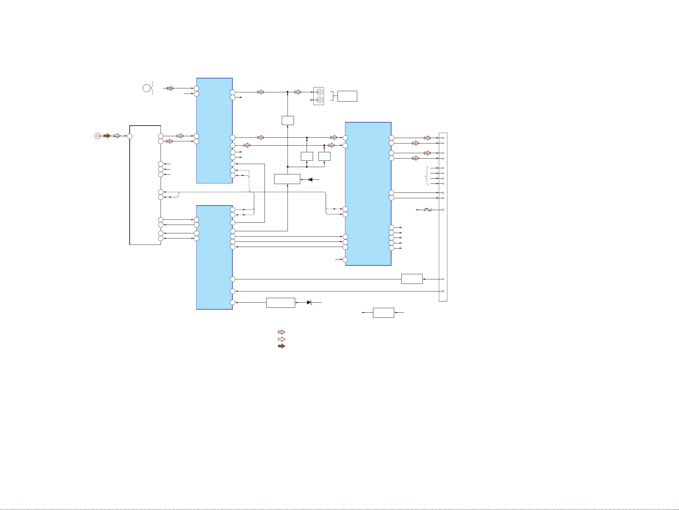
3-3. BLOCK DIAGRAM — MAIN SECTION —
ELECTRONIC VOLUME
IC401
CDX-S2000/S2000S/SW200
PJ601
(ANTENNA)
CD
SECTION
(Page 18)
TUX601
(TUNER UNIT)
1
ANT
A
VCC
TU VDD
E2P VDD
TU-SCL
TU-SDA
S-METER
TU MUTE
E2P SCL
E2P SDA
CD-L
L
R
4
3
10
11
15
13
14
6
7
16
17
R-CH
AU+8V
TU+5V
U COM+3.3V
SCL
SDA
9
C2
8
C1
7
B2
6
B1
SYSTEM CONTROL
IC801 (2/3)
45
VSM
15
TU ATT
25
EEP SCK
24
EEP SIO
OUTS1
OUTS2
OUTF2
OUTR2
OUTF1
OUTR1
MUTE
SCL
SDA
IIC SCK
IIC SIO
VOL ATT
ATT
BEEP
STB
DIAG
17
18
23
22
25
24
29
30
31
33
34
6
1
5
31
56
R-CH
R-CH (FRONT)
R-CH (REAR)
SCL
SDA
SCL
SDA
MUTE
Q407
MUTE CONTROL
Q400,401
R-CH
MUTE
Q405
D400
MUTE
Q404
BATT
L
R
BATT
SDA
SCL
PJ401
REAR
AUDIO OUT
12
INRR(FL)
11
INRF(RL)
2
SDA
4
SCL
16
ACGND
22
STB
25
DIAG
35
VP
POWER AMP
IC100
PR+
PR-
RF+
RF-
SW1
SW2
REG1
REG2
REG3
REG4
REG5
29
27
30
37
31
33
34
5
3
9
7
R-CH
BATT
AU+8V
U-COM+3.3V
SERVO+3.3V
MECHA+6V
DISP+B
F901
CNP901
10
12
11
16
1
FL+
9
FL-
2
RL+
RL-
4
FR+
FR-
3
RR+
RR-
5
AMP-REM
6
ANT-REM
ACC IN
TEST IN
BU IN
64
67
: CD PLAY
: FM
: AM
D912
BATT
TU+5V
TU+5V REG
Q601
53
BATTERY CHECK
Q902,906,907
• R-CH is omitted due to same as L-CH.
• Signal Path
ACC CHECK
Q900
AU+8V
7
ACC
15
TEST
19 19
Page 20

CDX-S2000/S2000S/SW200
)
3-4. BLOCK DIAGRAM — DISPLAY SECTION — 3-5. CIRCUIT BOARDS LOCATION
KEY MATRIX
LSW905-911,913,
914,916-920,
S901-906
E model
S800
FREQUENCY
()
SELECT
U COM+3.3V
SYSTEM CONTROL
IC801 (3/3)
LCD DRIVER
IC901
SERVO board
SENSOR board
KEYIN0
D801
KEY
ACKNOWLEDGE
SWITCH
Q800
38
39
47
75
KEYIN1
KEY ACK
XKEY ON
LCD SO
LCD SCK
LCD CE
28
64
DI
SEG4
4
SEG49
COM4
COM1
DIMMER
|
|
49
51
|
|
54
CL
29
27
CLK
63
CE
CE
62
LCD901
LIQUID
CRYSTAL
DISPLAY
PANEL
LED910,911
LCD
(
BACK LIGHT
)
SPEAKER board
tuner unit
(TUX601
DISP+B
LED901,902,904-909,
LSW905-911,913,914,
3
+3.3V REG
IC905
V OUT
916-920
VDD
CE
2
DISP+B
4
DST SEL
S802
RESET
46
REMOTE CONTROL
SIGNAL RECEIVER
IC951
1
RESET
77
X1A
79
X0A
80
SIRCS
65
82
X0
X1
83
OUT
2
X800
3.68MHz
VCC
IR
9K
10K
1
US,Canadian
model
X801
32.768kHz
RESET
IC802
OUT
2
IN
DISPLAY board
MAIN board
2020
Page 21

3-6. NOTE FOR PRINTED WIRING BOARDS AND SCHEMATIC DIAGRAMS 3-7. WAVEFORMS
CDX-S2000/S2000S/SW200
THIS NOTE IS COMMON FOR PRINTED WIRING
BOARDS AND SCHEMATIC DIAGRAMS.
(In addition to this, the necessary note is printed
in each block.)
For schematic diagrams.
Note:
• All capacitors are in µF unless otherwise noted. pF: µµF
50 WV or less are not indicated except for electrolytics
and tantalums.
• All resistors are in Ω and 1/
specified.
f
•
• C : panel designation.
• A : B+ Line.
• B : B– Line.
• H : adjustment for repair.
•Voltages and waveforms are dc with respect to ground
• CD mechanism section
no mark : CD PLAY
• Main (1/2), (2/2) and Display sections
no mark : FM
: internal component.
Note:
The components identified by mark 0 or dotted
line with mark 0 are criti-
cal for safety.
Replace only with part
number specified.
under no-signal (detuned) conditions.
(): AM
<>: CD PLAY
4
W or less unless otherwise
Note:
Les composants identifiés par
une marque 0 sont critiques
pour la sécurité.
Ne les remplacer que par une
piéce portant le numéro
spécifié.
∗ : Impossible to measure
•Voltages are taken with a VOM (Input impedance 10 MΩ).
Voltage variations may be noted due to normal production tolerances.
•Waveforms are taken with a oscilloscope.
Voltage variations may be noted due to normal production tolerances.
• Circled numbers refer to waveforms.
• Signal path.
J : CD PLAY
F : FM
f : AM
• Abbreviation
CND : Canadian model.
For printed wiring boards.
Note:
• X : parts extracted from the component side.
• Y : parts extracted from the conductor side.
a
•
• : Pattern from the side which enables seeing.
(The other layers' patterns are not indicated.)
Caution:
Pattern face side: Parts on the pattern face side seen from the
(Side B) pattern face are indicated.
Parts face side: Parts on the parts face side seen from the
(Side A) parts face are indicated.
• Abbreviation
: Through hole.
C
Q
These are omitted
EB
E
CB
These are omitted
C
BE
These are omitted
CND : Canadian model.
— Servo Board —
(MODE: CD PLAY)
1
16.9344MHz
IC1 wd (XTAL)
2
uj
(AGCI)
IC1
3
Approx. 620mVp-p
od
(FEO)
IC1
4
Approx. 200mVp-p
oh
(TEO)
IC1
1.2Vp-p
1.6Vp-p
0V
0V
— Main Board —
1
32.768kHz
IC801 i; (X0A)
2
3.68MHz
IC801
is
1.7Vp-p
2.4Vp-p
(X0)
21 21
Page 22

CDX-S2000/S2000S/SW200
3-8. PRINTED WIRING BOARDS — CD MECHANISM SECTION — • Refer to page 20 for Circuit Boards Location. : Uses unleaded solder.
A
B
C
D
1
234567891011 12 13 14
C6
R42
C5
FB1
R41
IC1
R6
C3
C19
R45
R7
C18
R44
C1
C21
C23
R9
C32
C27
C25
C36
C26
C31
C30
R13
C28
C39
C29
C38
Q1
R15
R11
R14
C34
R12
C37
C35
CN2
CN1
(Page 26)
C2
C20
JR91
JR90
JR40
C11
C13
JR41
C8
X1
C7
R1
C17
E
F
G
R74
R76
R72
R77
R70
R75
R71
R73
C73
C72
C75
C71
C70
IC2
C78
C77
C76
C79
R83
C74
R85
R84
R81
R79
R82
R80
R78
SW1
SW3
SW2
1-688-822-
2222
Page 23
• Refer to page 21 for Waveforms.
3-9. SCHEMATIC DIAGRAM — CD MECHANISM SECTION — • Refer to page 29 for IC Block Diagram.
CDX-S2000/S2000S/SW200
C20
SW3
SW2
CN2
TP27
TP28
TP29
TP31
TP30
TP29
TP14
TP28
TP27
TP26
TP19 C18
Q1
R13
C36
C37
R12
C35
C34
R11
SW4
M901
M902
TP81
TP80
SW1
TP85
TP83
TP84
TP82
TP87
TP88
TP89
TP90
TP91
R14 R15
C38
TP33TP32
TP20
C39
C28
TP22
C29
C26
TP21
C27
TP23
C30
TP24
TP25
C31
C32
C1
R9
C23
C25
C2
R7
C21
R6
C19
IC1
C5
C3
C6
C7
C17
R1
C13
TP13
TP12
TP11
TP10
TP9
TP8
TP7
TP6
TP5
TP4
TP3
TP2
TP1
C11
JR91
JR90
X1
C8
FB1
R41
JR41
JR40
R42
TP65
TP64
TP63
TP62
TP61
TP60
R45
TP59
R44
TP58
TP57
TP56
TP55
TP54
TP48
TP52
TP51
TP53
TP49
TP50
TP47
TP46
TP45
TP44
TP43
TP42
TP41
TP40
CN1
(Page 25)
M903
TP92
TP93
R70 R71
R72
R74 R75
R76
C70
C71
R73
C72
C73
R77
TP100
TP71
TP70
TP73
TP72
IC B/D
C74
IC2
C79
R85
R84
R82R83
C78
C77
R80R81
C76
R78R79
TP75
TP74
C75
23 23
Page 24

CDX-S2000/S2000S/SW200
3-10. SCHEMATIC DIAGRAM — MAIN SECTION (1/2) — • Refer to page 30 for IC Block Diagram.
TUX601
PJ601
R401
R400
C400
C600
JR103
C414
C409
C408
C411
C410
Q601
IC B/D
IC401
L602
R606
R412
R411
R409
R407
R406
R405
R404
R435
R436
L400
C416
R604
JR10
C417
R603
R608
R607
C453
C428
C452
R441
R443
C424
C426
C425
R417
R416
R415
R414
R440
C435
C436
C303
D907
D908
D909
D917
C108
D916
CNP901
IC100
R431
R421
R420
R419
R418
JR6
R442
Q407
Q405
Q404
Q403
Q402
Q406
C440
C444
C438
C437
R432
R429
R427
C113
C106
C101
C107
D921
D922
D904
D903
D902
D905
D906
PJ401
C621
C619C618
D600 Q400
R615
C620
Q401
(Page 25)
C430
D400
R424
R902
Q900
R903
C908
R904
C111
C109
C922
R931
R932
R913
D914
F901
L900
D919
2424
Page 25

3-11. SCHEMATIC DIAGRAM — MAIN SECTION (2/2) — • Refer to page 21 for Waveforms.
CDX-S2000/S2000S/SW200
(Page 24)
(Page 23)
CN751
C709
C705
C701
C704 R722
CNP800
C707
L702
L701
L700
R708
R709
R707
R703
JR11
R843
R802
R851
S800
R815
R800
R808
R806
C807
C823
C824
R809
R805
C813
R801
R804
R850
R826
R832R834
R819
R818
C821
R849
R821
R823
R822
D801
R835
R447
1
84
840
839
R
R
R
830
828
R
R
IC801
R852
R848
R844
C446
R873
C447
C441
R448
C816 C817
C812
D702
R854
X801
C802
C801
R845
R860
R936
R853
R705
C822
X800
IC802
C810
C820
C818
R837
C825
C809
R838
R846
R847
R810
R811
JR5
(Page 28)
D817
R833
813
814
815
812
D811
D
D
D816
D
D
R814
Q800
R927
C706
Q906
R825
C815
R824
Q907
D808
R437
C909
R901R925
S802
R917 R928
R912
D912D915
Q902
25 25
Page 26

CDX-S2000/S2000S/SW200
3-12. PRINTED WIRING BOARDS — MAIN SECTION — • Refer to page 20 for Circuit Boards Location. : Uses unleaded solder.
A
B
C
D
E
F
G
H
J
1
606
R
608
R
607
R
47
JW
JW
I
4
JW
23456789101112131415
J401
P
1
J60
P
CN
P
435
C
436
C
3
30
C
8
10
C
5
6
JW
JW
600
C
130
L602
615
R
60
JW
59
JW
58
JW
604
R
603
R
601
X
TU
48
815
R
3
JW
JW
415
C618
601
Q
619
C
10
JR
15
8
817
D
D
R
620
C
600
D
61
JW
54
52
JW
JW
51
JW
50
JW
813
816
814
D
D
D
C444
43
4
R
407
Q
441
R
20
4
R
404
Q
JW
403
Q
440
414
R
R
426
C
453
C
436
R
409
R
408
C
53
55
JW
JW
46
JW
812
811
D
D
800
P
N
C
42
4
R
421
R
418
R
37
440
C
419
R
405
Q
406
Q
127
JW
128
401
Q
400
D
416
R
425
C
424
C
435
R
452
C
411
R
412
R
56
JW
45
JW
44
JW
405
404
406
R
R
R
401
IC
409
C
57
JW
S
800
3
4
42
JW
JW
C4
431
R
9
42
R
438
C
402
Q
JR
400
Q
417
R
407
R
41
JW
JW
JW
R
106
C
6
432
R
121
JW
430
C
424
R
428
C
L400
416
C
808
R
800
R
40
JW
136
137
833
417
C
39
JW
C411
R
C
400
C
103
JR
4
B
FM
38
JW
28
JW
3
11
C
126
JW
125
JW
124
JW
123
JW
101
C
107
C
122
JW
120
JW
446
C
447
447
C441
66
JW
401
R
JW
400
R
410
C
414
C
35
JW
7
3
36
JW
JW
809
R
2
3
JW
118
JW
111
C
448
R
63
1
C80
67
JW
62
JW
34
JW
834
R
31
JW
64
JW
33
R
JW
828
R
3
82
R
821
R
819
R
832
R
818
R
824
C
06
805
8
R
R
823
C
801
R
30
29
JW
JW
6
2
JW
801
850
R
D
12
1
13
1
JW
JW
904
D
117
116
JW
JW
927
R
837
R
142
JW
802
C
JW
839
R
830
822
R
813
C
C
7
2
JW
804
R
R
27
4
R
11
1
JW
100
IC
JW
JW
6
7
905
D
115
JW
C809
141
JW
810
C
135
65
JW
840
841
R
R
807
C
821
826
R
849
800
Q
71
JW
90
90
D
D
922
D
921
D
114
JW
109
C
140
JW
68
JW
702
D
JW
JW
JW
0
7
69
JW
JW
IC801
706
C
25
24
23
JW
JW
JW
902
D
0
11
JW
08
1
9
10
7
10
JW
106
JW
908
D
909
D
04
105
1
JW
JW
L700
76
74
73
JW
143
72
JW
7
70
C
10
JW
R
707
R
843
722
802
R
R
R
R
705
R
R
800
X
818
C
854
R
801
X
21
22
JW
19
JW
20
JW
JW
802
S
901
903
D
JW
91
JW
701
C
09
7
C
838
846
853
C
18
JW
01
F9
8
9
JW
916
D
17
9
D
931
R
932
R
100
1
103
2
10
10
JW
JW
JW
751
N
C
708
R
822
C
936
R
820
C
3
B
FM
817
C
873
816
R
C
812
814
R
6
17
1
15
JW
JW
JW
437
R
815
C
13
9
R
99
JW
914
D
22
C9
847
R
860
R
14
JW
919
D
94
JW
JW
92
JW
88
JW
2
91
R
01
L7
702
L
811
R
78
JW
705
C
9
7
JW
851
R
25
5
JR
8
C
901
R
848
R
844
R
JW
R
13
JW
808
D
86
JW
704
C
709
R
11
JR
11
W
001
TP
J
R
12
845
9
13
JW
85
JW
84
JW
10
8
R
JW
703
R
904
R
7
JW
3
90
R
925
R
49
JW
852
02
IC8
93
8
92
R
81
Q900
97
JW
96
JW
95
JW
L900
C909
7
915
D
91
R
87
JW
902
Q
912
D
907
Q
906
Q
4
25
2
8
8
R
R
(Page 22)
206
JW
205
JW
202
JW
201
JW
207
JW
204
JW
203
JW
200
JW
• Semiconductor Location
Ref. No. Location
D400 D-4
80
JW
D600 E-2
D801 I-5
Ref. No. Location
D919 D-9
D921 D-7
D922 D-7
D808 J-9
835
R
908
C
02
9
R
8
JW
9
JW
1
2
JW
JW
D811 I-3
D812 I-3
D813 I-3
D814 I-3
D815 I-2
D816 I-2
D817 I-2
D902 B-8
D903 B-8
D904 C-6
D905 C-6
D906 C-7
D907 C-7
D908 C-7
D909 C-7
D912 F-11
D914 C-9
D915 E-10
D916 C-8
IC100 B-6
IC401 F-4
IC801 H-7
IC802 H-10
Q400 D-4
Q401 D-4
Q402 C-4
Q403 D-3
Q404 C-3
Q405 C-4
Q406 C-4
Q407 C-3
Q601 E-2
Q800 I-6
Q900 H-10
Q902 E-11
Q906 F-11
Q907 F-11
D917 C-8
(Page 27)
2626
Page 27

3-13. PRINTED WIRING BOARD — DISPLAY SECTION — • Refer to page 20 for Circuit Boards Location. : Uses unleaded solder.
CDX-S2000/S2000S/SW200
A
B
C
D
1
LSW905
LSW906
23456789101112131415
LED906
S901
LED907
LED904
S904
LED905
S905
LED910
LSW907
LSW908
LSW909
LSW910
LSW911
LCD901
LSW920
LSW919
LSW918
LSW917
LED909
LED911
LED901
S903
LED902
S906
LSW916
LED908
S902
LSW913
LSW914
IC951
E
F
G
H
(Page 26)
C955
D902
C951
R974
R951
R917
R916
R915
CN901
R976
R980
R986
R952
R968
R969
R977
R981
R914
R913
R912
R985
R901
R978
R982
R983
R973
R907
R906
R905
R904
R903
R979
R902
R966
R908
R967
R909
R910
R975
R972
R919
R955
FMB3
R956
R954
R953
IC901
C952
R960
R959
FMB4
R958
C950
R957
R961
C953
D903
D905
R918
D951
C956
D904
IC905
• Semiconductor Location
I
Ref. No. Location
D902 F-11
D903 F-9
D904 F-9
D905 F-9
D951 F-9
IC901 G-8
Ref. No. Location
IC905 G-10
IC951 D-14
LED901 C-13
LED902 C-13
LED904 C-3
LED905 C-3
Ref. No. Location
LED906 A-2
LED907 A-2
LED908 A-14
LED909 A-13
LED910 C-4
LED911 C-12
27 27
Page 28

CDX-S2000/S2000S/SW200
3-14. SCHEMATIC DIAGRAM — DISPLAY SECTION —
(Page 25)
CN901
R966 R967
LED910
LED911
R968 R969
D902
D903
D904
R912 R913 R914 R915 R916
LSW913(1/2)
914(1/2)
LSW
S906
916(2/2)
LSW
R972 R974 R976 R986 R980 R982 R978
LSW910(1/2)
LSW909(1/2)
LSW908(1/2)
LSW907(1/2)
917(2/2)
LSW
LSW918(1/2)
LSW919(1/2)
LSW920(1/2)
LSW911(1/2)
R917 R918 R919
918(2/2)
919(2/2)
W
LSW
LS
LSW917(1/2)
LSW916(1/2)
920(2/2)
LSW
LED902
LED901
R977R985
911(2/2)
W
LS
LSW914(2/2)
LSW913(2/2)
LED908 LED906
LSW906(2/2)
LSW905(2/2)
LED907LED909
R983R981R975R973
R979
LED904
LED905
R952
IC951
C951
D951
R958
R959
R951
R960
C950
D905
C953 R957
R954
R955
R956
R961
IC905
C956
C955
IC901
R953
C952
R901 R902 R903 R904 R905
902
S903
S
S904
S905
S901
R906 R907 R908 R909 R910
908(2/2)
907(2/2)
LSW905(1/2)
906(1/2)
LSW
LSW
LSW
909(2/2)
LSW
LCD901
910(2/2)
LSW
2828
Page 29

3-15. IC BLOCK DIAGRAMS
IC2 BA5966FP-FE2 (SERVO Board)
REV
OPIN4(+)
OPIN4(–)
2728 26 25
OPOUT4
CDX-S2000/S2000S/SW200
OPIN3(+)
OPIN3(–)
24 23 22 21 20 19 18 17 16 15
OPOUT3
MUTE
BIAS
GND
VO3(–)
VO3(+)
VO4(–)
VO4(+)
LOADING DRIVER
REV
FWD
FWD
+–
OUT F
OUT R
+–+–
4 5 6 7 8 9 10 11 12 13 1421 3
OPIN1(–)
OPOUT1
OPIN1(+)
+–
–
+
+
–
OPIN2(+)
OPIN2(–)
OPOUT2
MUTE
+–
+–
+
VOL(+)
–
LEVEL
SHIFT
LEVEL
SHIFT
–+
+–
+–
VO2(–)
VO2(+)
–
+
+
–
VCC
VCC
VOL(–)
+–
–
LEVEL
SHIFT
LEVEL
SHIFT
–
+–
VO1(–)
+–
+
+
+–
VO1(+)
29
Page 30

CDX-S2000/S2000S/SW200
IC401 BD3808FS (MAIN Board)
DGND
SDA
SCL
32 31 30 29 28 27 26 25 24 23 22
MUTE
SEL
ADJ
VCC
VCC
OUTF1
OUTR1
OUTF2
OUTR2
DS12
DS22
21 20 19 18 17
DS32
OUTS1
OUTS2
2
I
C BUS
LOGIC
BASS
fo:60,70,80,100,120,140,160,200Hz
Q:0.5,0.75,1,1.25
MIDDLE
fo:500Hz,1kHz
Q:1
TABLE
fo:5,7.5,10,12.5kHz
VCO
FADER
(0~-58,
-∞dB)
EFFECT (0dB~
+20dB,2dB STEP)
TONE
PASS
(+23~-79dB,-∞dB
fc:40kHz fc:40kHz
(0~15dB,1dB STEP)
(4 STEREO INCLUDE 1 ISOLATION INPUT)
FADER
(0~-58,
-∞dB)
TONE
PASS
BASS,TREBLE, MIDDLE
(-15dB~+15dB,1dB STEP)
VOLUME
1dB STEP)
ANTI-ALIASING
FILTER
INPUT GAIN
MUTE
INPUT SELECTOR
FADER
(0~-58,
-∞dB)
EFFECT (0dB~
+20dB,2dB STEP)
BASS,TREBLE, MIDDLE
(-15dB~+15dB,1dB STEP)
VOLUME
(+23~-79dB,-∞dB
1dB STEP)
ANTI-ALIASING
FILTER
INPUT GAIN
(0~15dB,1dB STEP)
MUTE
FADER
(0~-58,
-∞dB)
2ND ORDER LPF
fc:OFF,80,120,160Hz
Q: 0.707
MIX
GAIN+ATT
(+10~-29,
-∞dB)
2ND ORDER
LPF
AGND
VCC/2
6 7 8 9 10 113 4 521
AP1
AN
FIL
AP2
B1
B2
C2
C1
D1
D2
12 14 1613 15
DS11
DS21
DS31
NC
NC
30
Page 31

NOTE:
2
• The mechanical parts with no reference
number in the exploded views are not supplied.
• Items marked “*” are not stocked since
they are seldom required for routine service.
Some delay should be anticipated
when ordering these items.
• -XX and -X mean standardized parts, so
they may have some difference from the
original one.
4-1. MAIN SECTION
SECTION 4
EXPLODED VIEWS
• Color Indication of Appearance Parts
Example :
KNOB, BALANCE (WHITE) ... (RED)
RR
Parts Color Cabinet’s Color
• Accessories are given in the last of this
parts list.
•Abbreviation
CND : Canadian model
CDX-S2000/S2000S/SW200
The components identified by
mark 0 or dotted line with mark
0 are critical for safety.
Replace only with part number
specified.
Les composants identifiés par une
marque 0 sont critiques pour
la sécurité.
Ne les remplacer que par une piéce
portant le numéro spécifié.
A
#1
A
MG-611XA-186//K
B
5
6
#1
not supplied
F901
#
4
TUX601
3
#1
B
7
not supplied
2
#1
Ref. No. Part No. Description Remark
1 X-3384-407-1 PANEL (1) ASSY, SUB
23-231-472-01 SCREW (+B 2X4)
3 X-3382-588-1 LOCK ASSY (S)
43-246-006-31 COVER
53-922-535-11 SCREW (+BTT)
61-776-206-21 CORD (WITH CONNECTOR) (POWER)
#1
1
Ref. No. Part No. Description Remark
7 A-3283-403-A MAIN BOARD, COMPLETE (US,CND)
7 A-3283-423-A MAIN BOARD, COMPLETE (E)
F901 1-532-877-11 FUSE (BLADE TYPE) (AUTO FUSE) 10A
TUX601 A-3220-959-A TUNER UNIT (TUX-032)
#1 7-685-792-09 SCREW +PTT 2.6X6 (S)
#2 7-685-793-09 SCREW +PTT 2.6X8 (S)
31
Page 32

CDX-S2000/S2000S/SW200
4-2. FRONT PANEL SECTION
58
57
#3
LCD901
not supplied
55
51
59
not supplied
54
54
#3
56
not supplied
(DISPLAY board)
52
53
51 A-3372-782-A PANEL SUB ASSY, FRONT (S2000S)
51 X-3384-427-1 PANEL SUB ASSY, FRONT (S2000:US,CND)
51 X-3384-459-1 PANEL SUB ASSY, FRONT (SW200)
51 X-3384-460-1 PANEL SUB ASSY, FRONT (S2000:E)
52 X-3384-456-1 BUTTON ASSY (S) (S2000:US,CND/SW200)
52 X-3384-461-1 BUTTON ASSY (S) (S2000:E)
52 X-3384-739-1 BUTTON ASSY (S) (S2000S)
53 3-245-998-01 FILTER (IR)
54 3-246-002-01 PLATE (CD), LIGHT GUIDE
55 3-259-794-01 SPRING (RELEASE)
56 3-246-003-01 PANEL (CD), FRONT BACK
32
Ref. No. Part No. Description RemarkRef. No. Part No. Description Remark
57 X-3378-390-3 CASE ASSY (for FRONT PANEL)
58 A-3372-569-A PANEL OVERALL ASSY, FRONT
(S2000:US,CND)
58 A-3372-590-A PANEL OVERALL ASSY, FRONT (S2000:E)
58 A-3372-716-A PANEL OVERALL ASSY, FRONT (SW200)
58 A-3372-781-A PANEL OVERALL ASSY, FRONT (S2000S)
59 1-694-988-11 CONDUCTIVE BOARD, CONNECTION
LCD901 1-805-079-11 DISPLAY PANEL, LIQUID CRYSTAL (E)
LCD901 1-805-449-11 DISPLAY PANEL, LIQUID CRYSTAL (US,CND)
#3 7-685-106-19 SCREW +P 2X10 TYPE2 NON-SLIT
Page 33

4-3. CD MECHANISM SECTION (1)
(MG-611XA-186//K)
CDX-S2000/S2000S/SW200
not supplied
not supplied
102
not supplied
(SENSOR board)
not supplied
101
#4
103
104
106
105
108
107
Ref. No. Part No. Description Remark Ref. No. Part No. Description Remark
101 A-3372-455-A CHASSIS (T) SUB ASSY
102 3-253-729-01 SPRING (LTR), TENSION COIL
103 3-253-746-01 SPRING (DAMPER), COMPRESSION
104 3-253-746-11 SPRING (DAMPER), COMPRESSION
105 3-253-695-01 SPRING (KF), TENSION COIL
106 3-253-748-01 DAMPER (S)
107 3-352-758-31 SCREW (M1.7), TOOTHED LOCK
108 A-3283-350-A SERVO BOARD, COMPLETE
#4 7-627-552-87 SCREW, PRECISION +P 1.7X2.2
33
Page 34

CDX-S2000/S2000S/SW200
4-4. CD MECHANISM SECTION (2)
(MG-611XA-186//K)
154
(including M901)
155
156
157
#5
SW4
151
not supplied
153
152
M902
not supplied
158
not supplied
The components identified by
mark 0 or dotted line with mark
0 are critical for safety.
Replace only with part number
specified.
not supplied
Les composants identifiés par une
marque 0 sont critiques pour
la sécurité.
Ne les remplacer que par une piéce
portant le numéro spécifié.
Ref. No. Part No. Description Remark Ref. No. Part No. Description Remark
151 A-3337-637-A CHASSIS (OP) COMPLETE ASSY
152 4-912-432-01 SCREW (B1.4X5), TAPPING
0 153 8-820-207-02 OPTICAL PICK-UP (KSS1000E/K1RP)
154 A-3337-640-A CHASSIS (OP) SUB ASSY (including M901)
155 A-3337-641-A ARM SUB ASSY, CHUCKING
156 A-3337-639-A LEVER (SL) SUB ASSY
157 X-3383-454-2 LEVER (SL) ASSY
158 3-261-959-01 SPRING (SL), TORSION
M902 A-3337-638-A MOTOR ASSY, SL (SLED)
SW4 1-571-099-11 SWITCH (1 KEY) (LIMIT)
#5 7-627-850-77 SCREW, PRECISION +P 1.4X1.8
34
Page 35

4-5. CD MECHANISM SECTION (3)
(MG-611XA-186//K)
CDX-S2000/S2000S/SW200
209
207
208
201
202
207
#4
M903
206
207
210
203
211
204
205
Ref. No. Part No. Description Remark Ref. No. Part No. Description Remark
201 3-338-647-31 WASHER (1.0-2.5)
202 3-259-024-01 WHEEL (RA), WORM
203 A-3337-633-A ARM ASSY, ROLLER
204 3-259-455-01 SPRING (RAL)
205 3-253-713-01 SPRING (RAR)
206 3-259-469-01 SPRING (LE), LEAF
207 2-134-636-31 SCREW (M1.7X2.5)
208 3-259-467-01 BRACKET (LEM)
209 3-345-648-91 SCREW (M1.4), TOOTHED LOCK
210 A-3372-456-A WORM (LEB) ASSY
211 3-259-468-01 BEARING (LEB)
M903 A-3372-454-A MOTOR ASSY, LE (LOADING)
#4 7-627-552-87 SCREW, PRECISION +P 1.7X2.2
35
Page 36
CDX-S2000/S2000S/SW200
4-6. CD MECHANISM SECTION (4)
(MG-611XA-186//K)
252
254
252
255
256
251
253
257
Ref. No. Part No. Description Remark Ref. No. Part No. Description Remark
251 3-259-429-01 WHEEL (LE), WORM
252 3-344-223-01 WASHER
253 3-259-470-01 GEAR (LE1)
254 3-253-755-01 LEVER (D)
255 3-899-829-01 WASHER (SLIT)
256 3-259-032-01 GEAR (LE2)
257 A-3372-453-A CHASSIS (M) BLOCK ASSY
36
Page 37

CDX-S2000/S2000S/SW200
SECTION 5
ELECTRICAL PARTS LIST
NOTE:
• Due to standardization, replacements in
the parts list may be different from the
parts specified in the diagrams or the
components used on the set.
• -XX and -X mean standardized parts, so
they may have some difference from the
original one.
• RESISTORS
All resistors are in ohms.
METAL:Metal-film resistor.
METAL OXIDE: Metal oxide-film resistor.
F:nonflammable
When indicating parts by reference
number, please include the board.
Ref. No. Part No. Description Remark Ref. No. Part No. Description Remark
DISPLAY BOARD
**************
1-694-988-11 CONDUCTIVE BOARD, CONNECTION
< CAPACITOR >
• Items marked “*” are not stocked since
they are seldom required for routine service.
Some delay should be anticipated
when ordering these items.
• SEMICONDUCTORS
In each case, u : µ, for example:
uA.. : µA.. uPA.. : µPA..
uPB.. : µPB.. uPC.. : µPC.. uPD.. : µPD..
• CAPACITORS
uF : µF
• COILS
uH : µH
•Abbreviation
CND : Canadian model
LED907 6-500-511-01 LED CL-270PG-C-TS (DISC IND L) (SW200)
LED907 8-719-082-38 LED CL-270SR-C-TS (DISC IND L)
LED908 6-500-510-01 LED CL-195PG-CD-T (Z) (SW200)
LED908 8-719-053-09 LED SML-310VT-T86 (Z) (S2000/S2000S)
LED909 6-500-511-01 LED CL-270PG-C-TS (DISC IND R) (SW200)
The components identified by
mark 0 or dotted line with mark
0 are critical for safety.
Replace only with part number
specified.
Les composants identifiés par une
marque 0 sont critiques pour
la sécurité.
Ne les remplacer que par une piéce
portant le numéro spécifié.
DISPLAY
(S2000/S2000S)
C950 1-107-826-11 CERAMIC CHIP 0.1uF 10% 16V
C951 1-164-227-11 CERAMIC CHIP 0.022uF 10% 25V
C952 1-125-891-11 CERAMIC CHIP 0.47uF 10% 10V
C953 1-162-927-11 CERAMIC CHIP 100PF 5% 50V
C955 1-107-826-11 CERAMIC CHIP 0.1uF 10% 16V
C956 1-125-837-11 CERAMIC CHIP 1uF 10% 6.3V
< CONNECTOR >
CN901 1-794-312-21 PIN, CONNECTOR 12P
< DIODE >
D902 8-719-069-54 DIODE UDZS-TE17-5.1B
D903 8-719-069-54 DIODE UDZS-TE17-5.1B
D904 8-719-069-54 DIODE UDZS-TE17-5.1B
D905 8-719-988-61 DIODE 1SS355TE-17
D951 8-719-069-54 DIODE UDZS-TE17-5.1B
< IC >
IC901 6-705-180-01 IC LC75827W
IC905 6-705-374-01 IC MM3033DULE
IC951 6-600-321-01 IC KSM-401Y (IR)
< LIQUID CRYSTAL DISPLAY >
LCD901 1-805-079-11 DISPLAY PANEL, LIQUID CRYSTAL (E)
LCD901 1-805-449-11 DISPLAY PANEL, LIQUID CRYSTAL (US,CND)
< DIODE >
LED901 6-500-510-01 LED CL-195PG-CD-T (OFF) (SW200)
LED901 8-719-053-09 LED SML-310VT-T86 (OFF) (S2000/S2000S)
LED902 6-500-510-01 LED CL-195PG-CD-T (EQ3) (SW200)
LED902 8-719-053-09 LED SML-310VT-T86 (EQ3) (S2000/S2000S)
LED904 6-500-510-01 LED CL-195PG-CD-T (SOURCE) (SW200)
LED904 8-719-053-09 LED SML-310VT-T86 (SOURCE)
(S2000/S2000S)
LED905 6-500-510-01 LED CL-195PG-CD-T (MODE) (SW200)
LED905 8-719-053-09 LED SML-310VT-T86 (MODE)
(S2000/S2000S)
LED906 6-500-510-01 LED CL-195PG-CD-T (SEL) (SW200)
LED906 8-719-053-09 LED SML-310VT-T86 (SEL) (S2000/S2000S)
LED909 8-719-082-38 LED CL-270SR-C-TS (DISC IND R)
(S2000/S2000S)
LED910 6-500-459-01 LED NSCW505T-ARS (LCD BACK LIGHT)
LED911 6-500-459-01 LED NSCW505T-ARS (LCD BACK LIGHT)
< SWITCH >
LSW905 1-762-619-21 SWITCH, KEYBOARD (WITH LED) (VOLUME +)
(SW200)
LSW905 1-771-476-11 SWITCH, KEYBOARD (WITH LED) (VOLUME +)
(S2000/S2000S)
LSW906 1-762-619-21 SWITCH, KEYBOARD (WITH LED) (VOLUME –)
(SW200)
LSW906 1-771-476-11 SWITCH, KEYBOARD (WITH LED) (VOLUME –)
(S2000/S2000S)
LSW907 1-771-609-31 SWITCH, TACTILE (WITH LED) (ATT) (SW200)
LSW907 1-771-883-31 SWITCH, TACTILE (WITH LED) (ATT)
(S2000/S2000S)
LSW908 1-771-609-31 SWITCH, TACTILE (WITH LED) (SENS)
(SW200)
LSW908 1-771-883-31 SWITCH, TACTILE (WITH LED) (SENS)
(S2000/S2000S)
LSW909 1-771-609-31 SWITCH, TACTILE (WITH LED) (1) (SW200)
LSW909 1-771-883-31 SWITCH, TACTILE (WITH LED) (1)
(S2000/S2000S)
LSW910 1-771-609-31 SWITCH, TACTILE (WITH LED) (2) (SW200)
LSW910 1-771-883-31 SWITCH, TACTILE (WITH LED) (2)
(S2000/S2000S)
LSW911 1-771-609-31 SWITCH, TACTILE (WITH LED) (3) (SW200)
LSW911 1-771-883-31 SWITCH, TACTILE (WITH LED) (3)
(S2000/S2000S)
LSW913 1-762-619-21 SWITCH, KEYBOARD (WITH LED)
(SEEK + > M) (SW200)
LSW913 1-771-476-11 SWITCH, KEYBOARD (WITH LED)
(SEEK + > M) (S2000/S2000S)
LSW914 1-762-619-21 SWITCH, KEYBOARD (WITH LED)
(SEEK m . –) (SW200)
LSW914 1-771-476-11 SWITCH, KEYBOARD (WITH LED)
(SEEK m . –) (S2000/S2000S)
LSW916 1-771-609-31 SWITCH, TACTILE (WITH LED) (DSPL)
(SW200)
LSW916 1-771-883-31 SWITCH, TACTILE (WITH LED) (DSPL)
(S2000/S2000S)
37
Page 38

CDX-S2000/S2000S/SW200
DISPLAY
Ref. No. Part No. Description Remark Ref. No. Part No. Description Remark
LSW917 1-771-609-31 SWITCH, TACTILE (WITH LED) (BTM) (SW200)
LSW917 1-771-883-31 SWITCH, TACTILE (WITH LED) (BTM)
(S2000/S2000S)
LSW918 1-771-609-31 SWITCH, TACTILE (WITH LED) (6) (SW200)
LSW918 1-771-883-31 SWITCH, TACTILE (WITH LED) (6)
(S2000/S2000S)
LSW919 1-771-609-31 SWITCH, TACTILE (WITH LED) (5) (SW200)
LSW919 1-771-883-31 SWITCH, TACTILE (WITH LED) (5)
(S2000/S2000S)
LSW920 1-771-609-31 SWITCH, TACTILE (WITH LED) (4) (SW200)
LSW920 1-771-883-31 SWITCH, TACTILE (WITH LED) (4)
(S2000/S2000S)
< RESISTOR >
R901 1-216-819-11 METAL CHIP 680 5% 1/10W
R902 1-216-819-11 METAL CHIP 680 5% 1/10W
R903 1-216-819-11 METAL CHIP 680 5% 1/10W
R904 1-216-821-11 METAL CHIP 1K 5% 1/10W
R905 1-218-851-11 RES-CHIP 1.5K 2% 1/16W
R975 1-216-808-11 METAL CHIP 82 5% 1/10W
(SW200)
R975 1-216-809-11 METAL CHIP 100 5% 1/10W
(S2000/S2000S)
R976 1-216-811-11 METAL CHIP 150 5% 1/10W
(SW200)
R976 1-216-813-11 METAL CHIP 220 5% 1/10W
(S2000/S2000S)
R977 1-216-811-11 METAL CHIP 150 5% 1/10W
(SW200)
R977 1-216-813-11 METAL CHIP 220 5% 1/10W
(S2000/S2000S)
R978 1-216-811-11 METAL CHIP 150 5% 1/10W
(SW200)
R978 1-216-813-11 METAL CHIP 220 5% 1/10W
(S2000/S2000S)
R979 1-216-811-11 METAL CHIP 150 5% 1/10W
(SW200)
R979 1-216-813-11 METAL CHIP 220 5% 1/10W
(S2000/S2000S)
R906 1-218-851-11 RES-CHIP 1.5K 2% 1/16W
R907 1-216-825-11 METAL CHIP 2.2K 5% 1/10W
R908 1-216-827-11 METAL CHIP 3.3K 5% 1/10W
R909 1-216-829-11 METAL CHIP 4.7K 5% 1/10W
R910 1-218-867-11 METAL CHIP 6.8K 5% 1/10W
R912 1-216-819-11 METAL CHIP 680 5% 1/10W
R913 1-216-819-11 METAL CHIP 680 5% 1/10W
R914 1-216-819-11 METAL CHIP 680 5% 1/10W
R915 1-216-821-11 METAL CHIP 1K 5% 1/10W
R916 1-218-851-11 RES-CHIP 1.5K 2% 1/16W
R917 1-218-851-11 RES-CHIP 1.5K 2% 1/16W
R918 1-216-825-11 METAL CHIP 2.2K 5% 1/10W
R919 1-216-827-11 METAL CHIP 3.3K 5% 1/10W
R951 1-216-815-11 METAL CHIP 330 5% 1/10W
R952 1-216-825-11 METAL CHIP 2.2K 5% 1/10W
R953 1-216-821-11 METAL CHIP 1K 5% 1/10W
R954 1-216-821-11 METAL CHIP 1K 5% 1/10W
R955 1-216-821-11 METAL CHIP 1K 5% 1/10W
R956 1-216-821-11 METAL CHIP 1K 5% 1/10W
R957 1-216-850-11 METAL CHIP 270K 5% 1/10W
R958 1-216-821-11 METAL CHIP 1K 5% 1/10W
R959 1-216-821-11 METAL CHIP 1K 5% 1/10W
R960 1-216-821-11 METAL CHIP 1K 5% 1/10W
R961 1-216-857-11 METAL CHIP 1M 5% 1/10W
R966 1-216-815-11 METAL CHIP 330 5% 1/10W
R967 1-216-815-11 METAL CHIP 330 5% 1/10W
R968 1-216-815-11 METAL CHIP 330 5% 1/10W
R969 1-216-815-11 METAL CHIP 330 5% 1/10W
R972 1-216-808-11 METAL CHIP 82 5% 1/10W
(SW200)
R972 1-216-809-11 METAL CHIP 100 5% 1/10W
(S2000/S2000S)
R980 1-216-808-11 METAL CHIP 82 5% 1/10W
(SW200)
R980 1-216-809-11 METAL CHIP 100 5% 1/10W
(S2000/S2000S)
R981 1-216-808-11 METAL CHIP 82 5% 1/10W
(SW200)
R981 1-216-809-11 METAL CHIP 100 5% 1/10W
(S2000/S2000S)
R982 1-216-808-11 METAL CHIP 82 5% 1/10W
(SW200)
R982 1-216-809-11 METAL CHIP 100 5% 1/10W
(S2000/S2000S)
R983 1-216-808-11 METAL CHIP 82 5% 1/10W
(SW200)
R983 1-216-809-11 METAL CHIP 100 5% 1/10W
(S2000/S2000S)
R985 1-216-811-11 METAL CHIP 150 5% 1/10W
(SW200)
R985 1-216-813-11 METAL CHIP 220 5% 1/10W
(S2000/S2000S)
R986 1-216-811-11 METAL CHIP 150 5% 1/10W
(SW200)
R986 1-216-813-11 METAL CHIP 220 5% 1/10W
(S2000/S2000S)
< SWITCH >
S901 1-771-884-31 SWITCH, TACTILE (SEL)
S902 1-771-884-31 SWITCH, TACTILE (Z)
S903 1-771-884-31 SWITCH, TACTILE (OFF)
S904 1-771-884-31 SWITCH, TACTILE (SOURCE)
S905 1-771-884-31 SWITCH, TACTILE (MODE)
S906 1-771-884-31 SWITCH, TACTILE (EQ3)
*************************************************************
R973 1-216-808-11 METAL CHIP 82 5% 1/10W
R973 1-216-809-11 METAL CHIP 100 5% 1/10W
(S2000/S2000S)
R974 1-216-808-11 METAL CHIP 82 5% 1/10W
R974 1-216-809-11 METAL CHIP 100 5% 1/10W
(S2000/S2000S)
38
(SW200)
(SW200)
Page 39

CDX-S2000/S2000S/SW200
MAIN
Ref. No. Part No. Description Remark Ref. No. Part No. Description Remark
A-3283-403-A MAIN BOARD, COMPLETE (including
SPEAKER BOARD) (US,CND)
A-3283-423-A MAIN BOARD, COMPLETE (including
SPEAKER BOARD) (E)
*********************
C812 1-107-826-11 CERAMIC CHIP 0.1uF 10% 16V
C813 1-124-584-00 ELECT 100uF 20% 10V
C815 1-162-964-11 CERAMIC CHIP 0.001uF 10% 50V
C816 1-164-160-11 CERAMIC CHIP 20PF 5% 50V
C817 1-162-918-11 CERAMIC CHIP 18PF 5% 50V
7-685-134-19 SCREW +P 2.6X8 TYPE2 NON-SLIT
7-685-793-09 SCREW +PTT 2.6X8 (S)
7-685-795-09 SCREW +PTT 2.6X12 (S)
< CAPACITOR >
C101 1-124-233-11 ELECT 10uF 20% 16V
C106 1-124-234-00 ELECT 22uF 20% 16V
C107 1-124-233-11 ELECT 10uF 20% 16V
C108 1-216-864-11 METAL CHIP 0 5% 1/10W
C109 1-124-233-11 ELECT 10uF 20% 16V
C111 1-124-233-11 ELECT 10uF 20% 16V
C113 1-107-823-11 CERAMIC CHIP 0.47uF 10% 16V
C303 1-216-864-11 METAL CHIP 0 5% 1/10W
C400 1-162-970-11 CERAMIC CHIP 0.01uF 10% 25V
C408 1-115-467-11 CERAMIC CHIP 0.22uF 10% 10V
C409 1-115-467-11 CERAMIC CHIP 0.22uF 10% 10V
C410 1-104-942-11 ELECT 1uF 20% 50V
C411 1-104-942-11 ELECT 1uF 20% 50V
C414 1-128-428-11 ELECT 10uF 20% 35V
C416 1-162-970-11 CERAMIC CHIP 0.01uF 10% 25V
C417 1-124-589-11 ELECT 47uF 20% 16V
C424 1-128-428-11 ELECT 10uF 20% 35V
C425 1-128-428-11 ELECT 10uF 20% 35V
C426 1-128-428-11 ELECT 10uF 20% 35V
C428 1-128-428-11 ELECT 10uF 20% 35V
C430 1-126-947-11 ELECT 47uF 20% 16V
C435 1-162-927-11 CERAMIC CHIP 100PF 5% 50V
C436 1-162-927-11 CERAMIC CHIP 100PF 5% 50V
C437 1-125-891-11 CERAMIC CHIP 0.47uF 10% 10V
C438 1-125-891-11 CERAMIC CHIP 0.47uF 10% 10V
C440 1-125-891-11 CERAMIC CHIP 0.47uF 10% 10V
C441 1-115-467-11 CERAMIC CHIP 0.22uF 10% 10V
C444 1-125-891-11 CERAMIC CHIP 0.47uF 10% 10V
C446 1-162-923-11 CERAMIC CHIP 47PF 5% 50V
C447 1-124-257-00 ELECT 2.2uF 20% 50V
C452 1-128-428-11 ELECT 10uF 20% 35V
C453 1-128-428-11 ELECT 10uF 20% 35V
C600 1-216-864-11 METAL CHIP 0 5% 1/10W
C618 1-126-786-11 ELECT 47uF 20% 16V
C619 1-124-247-61 ELECT 10uF 20% 35V
C620 1-107-826-11 CERAMIC CHIP 0.1uF 10% 16V
C621 1-115-156-11 CERAMIC CHIP 1uF 10V
C701 1-124-584-00 ELECT 100uF 20% 10V
C704 1-124-584-00 ELECT 100uF 20% 10V
C705 1-124-584-00 ELECT 100uF 20% 10V
C818 1-164-160-11 CERAMIC CHIP 20PF 5% 50V
C820 1-162-920-11 CERAMIC CHIP 27PF 5% 50V
C821 1-107-826-11 CERAMIC CHIP 0.1uF 10% 16V
C822 1-107-826-11 CERAMIC CHIP 0.1uF 10% 16V
C823 1-162-927-11 CERAMIC CHIP 100PF 5% 50V
C824 1-162-927-11 CERAMIC CHIP 100PF 5% 50V
C825 1-124-584-00 ELECT 100uF 20% 10V
C908 1-126-160-11 ELECT 1uF 20% 50V
C909 1-162-970-11 CERAMIC CHIP 0.01uF 10% 25V
C922 1-131-868-81 ELECT 3300uF 20% 16V
< CONNECTOR >
CN751 1-817-536-11 CONNECTOR, BOARD TO BOARD 28P
CNP800 1-794-311-21 PLUG, CONNECTOR 12P
CNP901 1-774-701-21 PIN, CONNECTOR 16P
< DIODE >
D400 8-719-988-61 DIODE 1SS355TE-17
D600 8-719-069-55 DIODE UDZS-TE17-5.6B
D702 1-216-864-11 METAL CHIP 0 5% 1/10W
D801 8-719-988-61 DIODE 1SS355TE-17
D808 8-719-978-33 DIODE DTZ-TT11-6.8B
D811 8-719-109-97 DIODE RD6.8ES-B2
D812 8-719-109-97 DIODE RD6.8ES-B2
D813 8-719-109-97 DIODE RD6.8ES-B2
D814 8-719-109-97 DIODE RD6.8ES-B2
D815 8-719-109-97 DIODE RD6.8ES-B2
D816 8-719-109-97 DIODE RD6.8ES-B2
D817 8-719-109-97 DIODE RD6.8ES-B2
D902 8-719-053-18 DIODE 1SR154-400TE-25
D903 8-719-053-18 DIODE 1SR154-400TE-25
D904 8-719-970-02 DIODE 1SR139-400
D905 8-719-970-02 DIODE 1SR139-400
D906 8-719-970-02 DIODE 1SR139-400
D907 8-719-970-02 DIODE 1SR139-400
D908 8-719-970-02 DIODE 1SR139-400
D909 8-719-970-02 DIODE 1SR139-400
D912 8-719-083-66 DIODE UDZS-TE17-18B
D914 8-719-978-33 DIODE DTZ-TT11-6.8B
D915 8-719-056-84 DIODE UDZ-TE-17-7.5B
D916 8-719-970-02 DIODE 1SR139-400
D917 8-719-970-02 DIODE 1SR139-400
D919 8-719-049-38 DIODE 1N5404TU
D921 8-719-970-02 DIODE 1SR139-400
D922 8-719-970-02 DIODE 1SR139-400
C706 1-162-964-11 CERAMIC CHIP 0.001uF 10% 50V
C707 1-124-584-00 ELECT 100uF 20% 10V
C709 1-162-964-11 CERAMIC CHIP 0.001uF 10% 50V
C801 1-107-826-11 CERAMIC CHIP 0.1uF 10% 16V
C802 1-124-589-11 ELECT 47uF 20% 16V
C807 1-162-970-11 CERAMIC CHIP 0.01uF 10% 25V
C809 1-124-584-00 ELECT 100uF 20% 10V
C810 1-125-701-11 DOUBLE LAYERS 0.047F 5.5V
< IC >
IC100 6-705-360-01 IC TDA8588BJ/N2
IC401 6-705-372-01 IC BD3808FS-FE2
IC801 6-803-819-01 IC MB90473PF-G165-BNDE1
IC802 8-759-659-13 IC PST3428UL
39
Page 40

CDX-S2000/S2000S/SW200
MAIN
Ref. No. Part No. Description Remark Ref. No. Part No. Description Remark
< JUMPER RESISTOR >
JR5 1-216-864-11 METAL CHIP 0 5% 1/10W
JR6 1-216-864-11 METAL CHIP 0 5% 1/10W
JR10 1-216-864-11 METAL CHIP 0 5% 1/10W
JR11 1-216-864-11 METAL CHIP 0 5% 1/10W
JR103 1-216-864-11 METAL CHIP 0 5% 1/10W
< COIL >
L400 1-414-398-11 INDUCTOR 10uH
L602 1-414-394-41 INDUCTOR 2.2uH
L700 1-410-501-11 INDUCTOR 2.2uH
L701 1-410-501-11 INDUCTOR 2.2uH
L702 1-410-509-11 INDUCTOR 10uH
L900 1-456-617-11 COIL, CHOKE 250uH
R436 1-216-809-11 METAL CHIP 100 5% 1/10W
R437 1-216-821-11 METAL CHIP 1K 5% 1/10W
R440 1-216-809-11 METAL CHIP 100 5% 1/10W
R441 1-216-809-11 METAL CHIP 100 5% 1/10W
R442 1-216-841-11 METAL CHIP 47K 5% 1/10W
R443 1-216-841-11 METAL CHIP 47K 5% 1/10W
R447 1-216-809-11 METAL CHIP 100 5% 1/10W
R448 1-216-841-11 METAL CHIP 47K 5% 1/10W
R603 1-247-807-31 CARBON 100 5% 1/4W
R604 1-247-807-31 CARBON 100 5% 1/4W
R606 1-216-809-11 METAL CHIP 100 5% 1/10W
R607 1-216-809-11 METAL CHIP 100 5% 1/10W
R608 1-216-809-11 METAL CHIP 100 5% 1/10W
R615 1-216-821-11 METAL CHIP 1K 5% 1/10W
R703 1-216-864-11 METAL CHIP 0 5% 1/10W
< JACK >
PJ401 1-774-698-11 JACK, PIN 2P (AUDIO OUT REAR)
PJ601 1-793-598-11 JACK (ANTENNA)
< TRANSISTOR >
Q400 8-729-027-46 TRANSISTOR DTC114YKA-T146
Q401 8-729-027-31 TRANSISTOR DTA124EKA-T146
Q402 6-550-752-01 TRANSISTOR DTC614TKT146
Q403 6-550-752-01 TRANSISTOR DTC614TKT146
Q404 6-550-752-01 TRANSISTOR DTC614TKT146
Q405 6-550-752-01 TRANSISTOR DTC614TKT146
Q406 6-550-752-01 TRANSISTOR DTC614TKT146
Q407 6-550-752-01 TRANSISTOR DTC614TKT146
Q601 8-729-106-68 TRANSISTOR 2SD1615A-GP
Q800 8-729-027-31 TRANSISTOR DTA124EKA-T146
Q900 8-729-901-81 TRANSISTOR 2SC2412K-T-146-R
Q902 8-729-900-53 TRANSISTOR DTC114EK
Q906 8-729-901-81 TRANSISTOR 2SC2412K-T-146-R
Q907 8-729-900-53 TRANSISTOR DTC114EK
< RESISTOR >
R404 1-216-809-11 METAL CHIP 100 5% 1/10W
R405 1-216-809-11 METAL CHIP 100 5% 1/10W
R406 1-216-809-11 METAL CHIP 100 5% 1/10W
R407 1-216-809-11 METAL CHIP 100 5% 1/10W
R409 1-216-839-11 METAL CHIP 33K 5% 1/10W
R411 1-216-809-11 METAL CHIP 100 5% 1/10W
R412 1-216-809-11 METAL CHIP 100 5% 1/10W
R414 1-216-809-11 METAL CHIP 100 5% 1/10W
R415 1-216-809-11 METAL CHIP 100 5% 1/10W
R416 1-216-809-11 METAL CHIP 100 5% 1/10W
R417 1-216-809-11 METAL CHIP 100 5% 1/10W
R418 1-216-841-11 METAL CHIP 47K 5% 1/10W
R419 1-216-841-11 METAL CHIP 47K 5% 1/10W
R420 1-216-841-11 METAL CHIP 47K 5% 1/10W
R421 1-216-841-11 METAL CHIP 47K 5% 1/10W
R424 1-216-805-11 METAL CHIP 47 5% 1/10W
R427 1-216-809-11 METAL CHIP 100 5% 1/10W
R429 1-247-807-31 CARBON 100 5% 1/4W
R431 1-247-807-31 CARBON 100 5% 1/4W
R432 1-216-809-11 METAL CHIP 100 5% 1/10W
R435 1-216-809-11 METAL CHIP 100 5% 1/10W
R705 1-216-809-11 METAL CHIP 100 5% 1/10W
R707 1-216-809-11 METAL CHIP 100 5% 1/10W
R709 1-216-864-11 METAL CHIP 0 5% 1/10W
R722 1-216-809-11 METAL CHIP 100 5% 1/10W
R800 1-216-841-11 METAL CHIP 47K 5% 1/10W
(E)
R801 1-216-809-11 METAL CHIP 100 5% 1/10W
R802 1-216-864-11 METAL CHIP 0 5% 1/10W
R804 1-216-809-11 METAL CHIP 100 5% 1/10W
R805 1-218-871-11 METAL CHIP 10K 0.5% 1/10W
R806 1-218-871-11 METAL CHIP 10K 0.5% 1/10W
R808 1-216-845-11 METAL CHIP 100K 5% 1/10W
(E)
R808 1-216-864-11 METAL CHIP 0 5% 1/10W
(US,CND)
R809 1-216-845-11 METAL CHIP 100K 5% 1/10W
(E)
R810 1-216-845-11 METAL CHIP 100K 5% 1/10W
R811 1-216-845-11 METAL CHIP 100K 5% 1/10W
R814 1-216-845-11 METAL CHIP 100K 5% 1/10W
R815 1-249-435-11 CARBON 33K 5% 1/4W
R818 1-216-809-11 METAL CHIP 100 5% 1/10W
R819 1-216-809-11 METAL CHIP 100 5% 1/10W
R821 1-216-817-11 METAL CHIP 470 5% 1/10W
R822 1-216-817-11 METAL CHIP 470 5% 1/10W
R823 1-216-817-11 METAL CHIP 470 5% 1/10W
R824 1-216-849-11 METAL CHIP 220K 5% 1/10W
R825 1-216-849-11 METAL CHIP 220K 5% 1/10W
R826 1-216-843-11 METAL CHIP 68K 5% 1/10W
R828 1-216-809-11 METAL CHIP 100 5% 1/10W
R830 1-216-809-11 METAL CHIP 100 5% 1/10W
R832 1-218-867-11 METAL CHIP 6.8K 5% 1/10W
R833 1-249-417-11 CARBON 1K 5% 1/4W
R834 1-218-867-11 METAL CHIP 6.8K 5% 1/10W
R835 1-216-845-11 METAL CHIP 100K 5% 1/10W
R837 1-216-864-11 METAL CHIP 0 5% 1/10W
R838 1-216-845-11 METAL CHIP 100K 5% 1/10W
R839 1-216-809-11 METAL CHIP 100 5% 1/10W
R840 1-216-809-11 METAL CHIP 100 5% 1/10W
R841 1-216-809-11 METAL CHIP 100 5% 1/10W
R843 1-216-809-11 METAL CHIP 100 5% 1/10W
R844 1-216-845-11 METAL CHIP 100K 5% 1/10W
R846 1-216-845-11 METAL CHIP 100K 5% 1/10W
R847 1-216-845-11 METAL CHIP 100K 5% 1/10W
40
Page 41

CDX-S2000/S2000S/SW200
MAIN SENSOR SERVO
Ref. No. Part No. Description Remark Ref. No. Part No. Description Remark
R848 1-216-845-11 METAL CHIP 100K 5% 1/10W
R849 1-216-841-11 METAL CHIP 47K 5% 1/10W
R850 1-218-871-11 METAL CHIP 10K 0.5% 1/10W
R851 1-216-809-11 METAL CHIP 100 5% 1/10W
R852 1-216-864-11 METAL CHIP 0 5% 1/10W
C19 1-107-826-11 CERAMIC CHIP 0.1uF 10% 16V
C20 1-107-826-11 CERAMIC CHIP 0.1uF 10% 16V
C21 1-162-970-11 CERAMIC CHIP 0.01uF 10% 25V
C23 1-162-923-11 CERAMIC CHIP 47PF 5% 50V
C25 1-162-908-11 CERAMIC CHIP 3PF 0.25PF 50V
R853 1-216-864-11 METAL CHIP 0 5% 1/10W
R854 1-216-864-11 METAL CHIP 0 5% 1/10W
R860 1-216-845-11 METAL CHIP 100K 5% 1/10W
R873 1-216-845-11 METAL CHIP 100K 5% 1/10W
R901 1-216-845-11 METAL CHIP 100K 5% 1/10W
R902 1-216-829-11 METAL CHIP 4.7K 5% 1/10W
R903 1-216-841-11 METAL CHIP 47K 5% 1/10W
R904 1-216-841-11 METAL CHIP 47K 5% 1/10W
R912 1-249-417-11 CARBON 1K 5% 1/4W
R913 1-216-821-11 METAL CHIP 1K 5% 1/10W
R917 1-249-421-11 CARBON 2.2K 5% 1/4W
R925 1-216-845-11 METAL CHIP 100K 5% 1/10W
R927 1-216-833-11 METAL CHIP 10K 5% 1/10W
R928 1-249-421-11 CARBON 2.2K 5% 1/4W
R931 1-216-073-00 RES-CHIP 10K 5% 1/10W
R932 1-216-073-00 RES-CHIP 10K 5% 1/10W
R936 1-216-864-11 METAL CHIP 0 5% 1/10W
< SWITCH >
S800 1-571-478-11 SWITCH, SLIDE (FREQUENCY SELECT) (E)
S802 1-692-431-21 SWITCH, TACTILE (RESET)
< TUNER >
TUX601 A-3220-959-A TUNER UNIT (TUX-032)
C26 1-107-826-11 CERAMIC CHIP 0.1uF 10% 16V
C27 1-107-826-11 CERAMIC CHIP 0.1uF 10% 16V
C28 1-107-826-11 CERAMIC CHIP 0.1uF 10% 16V
C29 1-107-826-11 CERAMIC CHIP 0.1uF 10% 16V
C30 1-162-921-11 CERAMIC CHIP 33PF 5% 50V
C31 1-162-925-11 CERAMIC CHIP 68PF 5% 50V
C32 1-107-826-11 CERAMIC CHIP 0.1uF 10% 16V
C34 1-107-826-11 CERAMIC CHIP 0.1uF 10% 16V
C35 1-162-970-11 CERAMIC CHIP 0.01uF 10% 25V
C36 1-162-967-11 CERAMIC CHIP 0.0033uF 10% 50V
C37 1-162-970-11 CERAMIC CHIP 0.01uF 10% 25V
C38 1-104-609-11 ELECT CHIP 100uF 20% 4V
C39 1-107-826-11 CERAMIC CHIP 0.1uF 10% 16V
C70 1-162-965-11 CERAMIC CHIP 0.0015uF 10% 50V
C71 1-162-965-11 CERAMIC CHIP 0.0015uF 10% 50V
C72 1-162-962-11 CERAMIC CHIP 470PF 10% 50V
C73 1-162-962-11 CERAMIC CHIP 470PF 10% 50V
C74 1-107-826-11 CERAMIC CHIP 0.1uF 10% 16V
C75 1-107-826-11 CERAMIC CHIP 0.1uF 10% 16V
C76 1-162-970-11 CERAMIC CHIP 0.01uF 10% 25V
C77 1-162-970-11 CERAMIC CHIP 0.01uF 10% 25V
C78 1-164-227-11 CERAMIC CHIP 0.022uF 10% 25V
C79 1-164-227-11 CERAMIC CHIP 0.022uF 10% 25V
< CONNECTOR >
< VIBRATOR >
X800 1-767-993-21 VIBRATOR, CRYSTAL (3.68MHz)
X801 1-813-202-11 VIBRATOR, CRYSTAL (32.768kHz)
*************************************************************
SENSOR BOARD
**************
< SWITCH >
SW2 1-529-566-61 SWITCH, PUSH (1 KEY) (SELF)
SW3 1-529-566-61 SWITCH, PUSH (1 KEY) (DISC IN)
*************************************************************
A-3283-350-A SERVO BOARD, COMPLETE
**********************
< CAPACITOR >
C1 1-107-826-11 CERAMIC CHIP 0.1uF 10% 16V
C2 1-162-970-11 CERAMIC CHIP 0.01uF 10% 25V
C3 1-107-826-11 CERAMIC CHIP 0.1uF 10% 16V
C5 1-107-826-11 CERAMIC CHIP 0.1uF 10% 16V
C6 1-100-381-11 ELECT CHIP 10uF 20% 16V
C7 1-107-826-11 CERAMIC CHIP 0.1uF 10% 16V
C8 1-107-826-11 CERAMIC CHIP 0.1uF 10% 16V
C11 1-107-826-11 CERAMIC CHIP 0.1uF 10% 16V
C13 1-107-826-11 CERAMIC CHIP 0.1uF 10% 16V
C17 1-107-826-11 CERAMIC CHIP 0.1uF 10% 16V
C18 1-162-970-11 CERAMIC CHIP 0.01uF 10% 25V
CN1 1-817-275-21 CONNECTOR, BOARD TO BOARD 28P
CN2 1-794-153-21 CONNECTOR, FPC (ZIF) 16P
< FERRITE BEAD >
FB1 1-414-760-21 FERRITE, EMI (SMD)
< IC >
IC1 6-703-699-01 IC uPD63712GC-8EU-A
IC2 6-705-002-01 IC BA5966FP-FE2
< FERRITE BEAD >
JR40 1-414-760-21 FERRITE, EMI (SMD)
JR41 1-414-760-21 FERRITE, EMI (SMD)
JR90 1-414-760-21 FERRITE, EMI (SMD)
JR91 1-414-760-21 FERRITE, EMI (SMD)
< TRANSISTOR >
Q1 8-729-904-87 TRANSISTOR 2SB1197K-R
< RESISTOR >
R1 1-216-841-11 METAL CHIP 47K 5% 1/10W
R6 1-216-833-11 METAL CHIP 10K 5% 1/10W
R7 1-216-840-11 METAL CHIP 39K 5% 1/10W
R9 1-216-822-11 METAL CHIP 1.2K 5% 1/10W
R11 1-216-833-11 METAL CHIP 10K 5% 1/10W
R12 1-216-809-11 METAL CHIP 100 5% 1/10W
R13 1-216-833-11 METAL CHIP 10K 5% 1/10W
41
Page 42

CDX-S2000/S2000S/SW200
SERVO
Ref. No. Part No. Description Remark Ref. No. Part No. Description Remark
R14 1-216-797-11 METAL CHIP 10 5% 1/10W
R15 1-216-797-11 METAL CHIP 10 5% 1/10W
R41 1-216-821-11 METAL CHIP 1K 5% 1/10W
R42 1-216-821-11 METAL CHIP 1K 5% 1/10W
R44 1-414-760-21 FERRITE, EMI (SMD)
R45 1-414-760-21 FERRITE, EMI (SMD)
R70 1-216-842-11 METAL CHIP 56K 5% 1/10W
R71 1-216-833-11 METAL CHIP 10K 5% 1/10W
R72 1-216-842-11 METAL CHIP 56K 5% 1/10W
R73 1-216-833-11 METAL CHIP 10K 5% 1/10W
R74 1-216-837-11 METAL CHIP 22K 5% 1/10W
R75 1-216-833-11 METAL CHIP 10K 5% 1/10W
R76 1-216-837-11 METAL CHIP 22K 5% 1/10W
R77 1-216-833-11 METAL CHIP 10K 5% 1/10W
R78 1-216-833-11 METAL CHIP 10K 5% 1/10W
R79 1-216-833-11 METAL CHIP 10K 5% 1/10W
R80 1-216-833-11 METAL CHIP 10K 5% 1/10W
R81 1-216-833-11 METAL CHIP 10K 5% 1/10W
R82 1-216-837-11 METAL CHIP 22K 5% 1/10W
R83 1-216-833-11 METAL CHIP 10K 5% 1/10W
301 X-3382-647-1 FRAME ASSY, FITTING
302 X-3366-972-2 SCREW ASSY (EXP), FITTING (E)
303 3-246-471-01 SCREW (+K 5X8 TP)
304 3-246-009-01 COLLAR
305 3-246-011-01 KEY (FRAME)
306 1-776-206-21 CORD (WITH CONNECTOR) (POWER)
PARTS FOR INSTALLATION AND CONNECTIONS
***************************************
302301
305303 306304
R84 1-216-837-11 METAL CHIP 22K 5% 1/10W
R85 1-216-833-11 METAL CHIP 10K 5% 1/10W
< SWITCH >
SW1 1-529-565-61 SWITCH, PUSH (1 KEY) (DOWN)
< VIBRATOR >
X1 1-795-562-21 VIBRATOR, CERAMIC (16.9344MHz)
*************************************************************
MISCELLANEOUS
***************
6 1-776-206-21 CORD (WITH CONNECTOR) (POWER)
0 153 8-820-207-02 OPTICAL PICK-UP (KSS1000E/K1RP)
154 A-3337-640-A CHASSIS (OP) SUB ASSY (including M901)
F901 1-532-877-11 FUSE (BLADE TYPE) (AUTO FUSE) 10A
M902 A-3337-638-A MOTOR ASSY, SL (SLED)
M903 A-3372-454-A MOTOR ASSY, LE (LOADING)
SW4 1-571-099-11 SWITCH (1 KEY) (LIMIT)
*************************************************************
ACCESSORIES
************
3-261-840-31 MANUAL, INSTRUCTION (ENGLISH,FRENCH)
3-261-840-41 MANUAL, INSTRUCTION (ENGLISH,SPANISH,
3-261-840-61 MANUAL, INSTRUCTION (ENGLISH,SPANISH)
3-261-841-31 MANUAL, INSTRUCTION, INSTALL (ENGLISH,
FRENCH) (S2000:US,CND)
3-261-841-41 MANUAL, INSTRUCTION, INSTALL (ENGLISH,
SPANISH,TRADITIONAL CHINESE)
(S2000:US,CND)
TRADITIONAL CHINESE)
(E)
(SW200)
(E)
3-261-841-61 MANUAL, INSTRUCTION, INSTALL (ENGLISH,
SPANISH) (SW200)
X-3378-390-3 CASE ASSY (for FRONT PANEL)
*************************************************************
42
The components identified by
mark 0 or dotted line with mark
0 are critical for safety.
Replace only with part number
specified.
Les composants identifiés par une
marque 0 sont critiques pour
la sécurité.
Ne les remplacer que par une piéce
portant le numéro spécifié.
Page 43

MEMO
CDX-S2000/S2000S/SW200
43
Page 44

CDX-S2000/S2000S/SW200
REVISION HISTORY
Clicking the version allows you to jump to the revised page.
Also, clicking the version at the upper on the revised page allows you to jump to the next revised page.
Ver. Date Description of Revision
1.0 2003. 11 New
44
 Loading...