SONY CDX-S2270EE Service Manual v.1.0
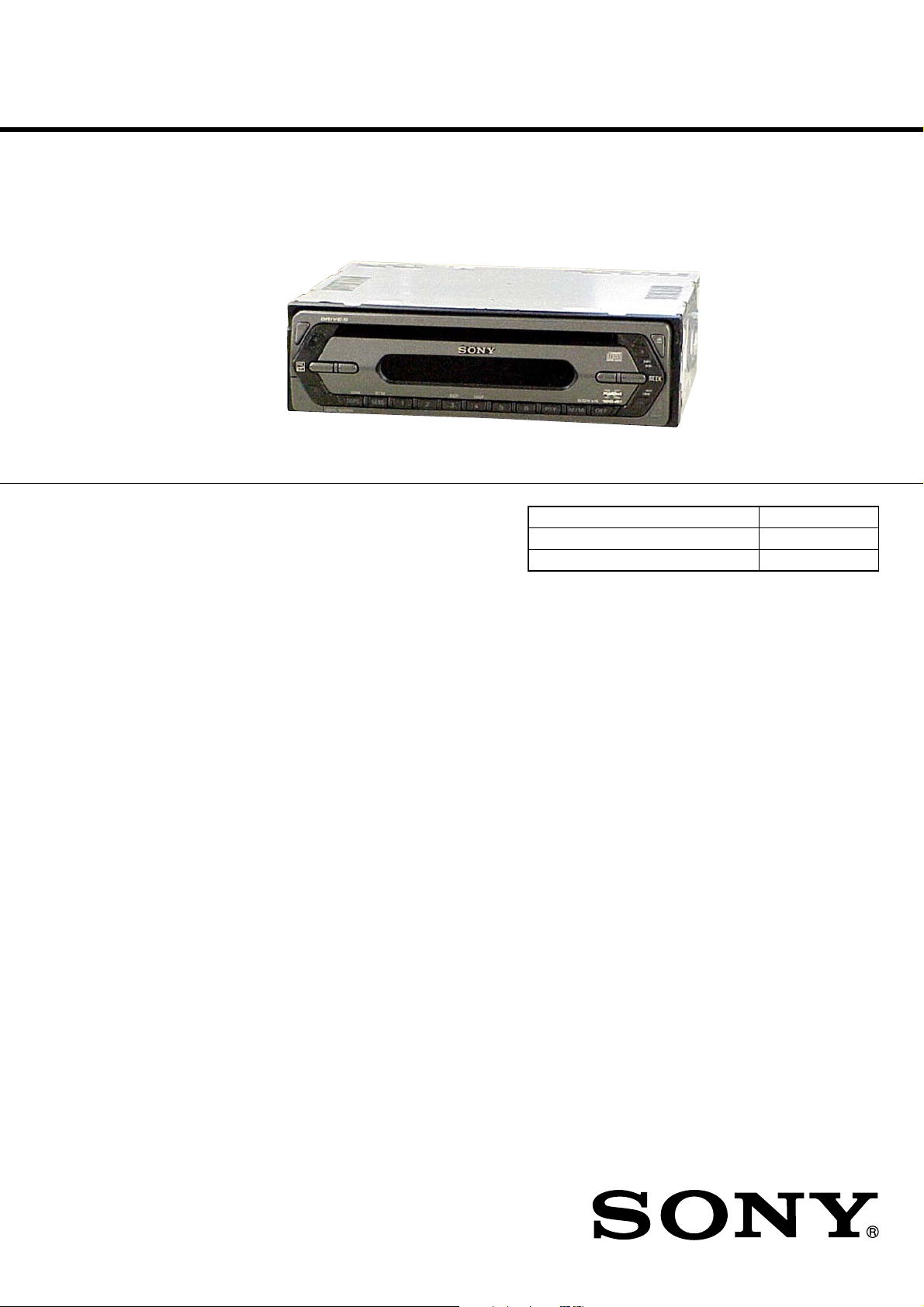
CDX-S2270EE
SERVICE MANUAL
Ver. 1.0 2006.01
• CDX-S2270EE is FM/AM compact disc player
in CXS-S2213GF.
• The tuner and CD sections have no adjustments.
SPECIFICATIONS
East European Model
Model Name Using Similar Mechanism CDX-R3350EE
CD Drive Mechanism Type MG-611TA-186//Q
Optical Pick-up Name KSS1000E
CD player section
Signal-to-noise ratio 120 dB
Frequency response 10 – 20,000 Hz
Wow and flutter Below measurable limit
Tuner section
FM
Tuning range FM1/FM2: 87.5 – 108.0 MHz (at 50 kHz step)
FM3: 65 – 74 MHz (at 30 kHz step)
Aerial terminal External aerial connector
Intermediate frequency 10.7 MHz/450 kHz
Usable sensitivity 9 dBf
Selectivity 75 dB at 400 kHz
Signal-to-noise ratio 67 dB (stereo),
69 dB (mono)
Harmonic distortion at 1 kHz
0.5% (stereo),
0.3% (mono)
Separation 35 dB at 1 kHz
Frequency response 30 – 15,000 Hz
AM
Tuning range 531 – 1,602 kHz
Aerial terminal External aerial connector
Intermediate frequency 10.7 MHz/450 kHz
Sensitivity 30 µV
Power amplifier section
Outputs Speaker outputs
(sure seal connectors)
Speaker impedance 4 – 8 ohms
Maximum power output 50 W × 4 (at 4 ohms)
General
Outputs Audio outputs terminal (sub/rear switchable)
Power aerial relay control terminal
Power amplifier control terminal
Input Aerial input terminal
Tone controls Low: ±10 dB at 60 Hz (XPLOD)
Mid: ±10 dB at 1 kHz (XPLOD)
High: ±10 dB at 10 kHz (XPLOD)
Power requirements 12 V DC car battery
(negative ground)
Dimensions Approx. 178 × 50 × 178 mm (w/h/d)
Mounting dimensions Approx. 182 × 53 × 161 mm (w/h/d)
Mass Approx. 1.2 kg
Supplied accessories Parts for installation and connections (1 set)
Front panel case (1)
Design and specifications are subject to change without
notice.
9-879-912-01
2006A04-1
© 2006.01
FM/AM COMPACT DISC PLAYER
Sony Corporation
eVehicle Division
Published by Sony Techno Create Corporation
CDX-S2270EE
SERVICE NOTES
NOTES ON HANDLING THE OPTICAL PICK-UP BLOCK
OR BASE UNIT
The laser diode in the optical pick-up block may suffer electrostatic
breakdown because of the potential difference generated by the
charged electrostatic load, etc. on clothing and the human body.
During repair, pay attention to electrostatic breakdown and also use
the procedure in the printed matter which is included in the repair
parts.
The flexible board is easily damaged and should be handled with
care.
NOTES ON LASER DIODE EMISSION CHECK
The laser beam on this model is concentrated so as to be focused on
the disc reflective surface by the objective lens in the optical pickup block. Therefore, when checking the laser diode emission,
observe from more than 30 cm away from the objective lens.
Notes on Chip Component Replacement
• Never reuse a disconnected chip component.
• Notice that the minus side of a tantalum capacitor may be damaged
by heat.
TEST DISCS
This set can playback CD-R and CD-ROM discs. The following
test discs should be used to check the capability:
CAUTION
Use of controls or adjustments or performance of procedures
other than those specified herein may result in hazardous
radiation exposure.
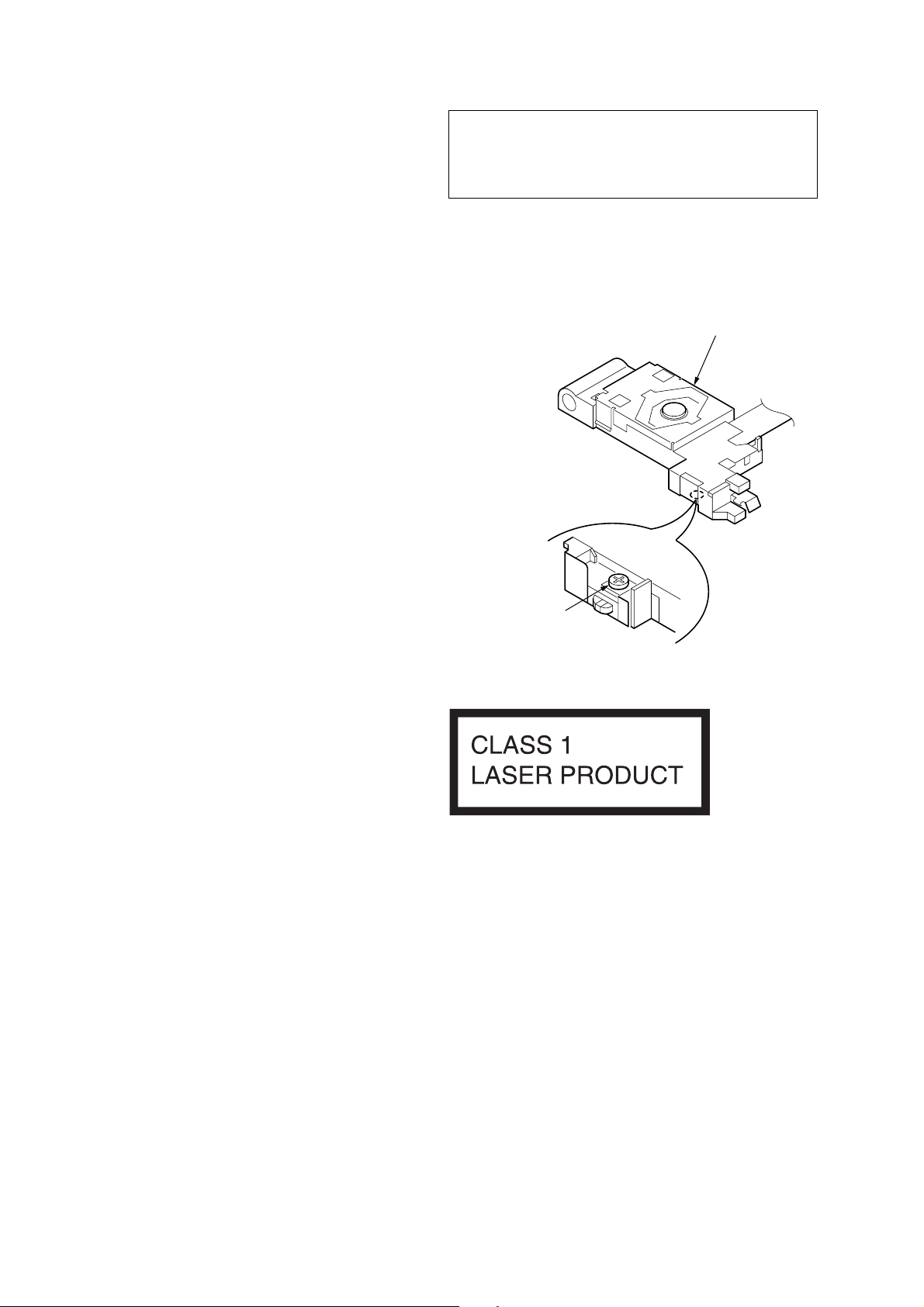
If the optical pick-up block is defective, please replace the whole
optical pick-up block.
Never turn the semi-fixed resistor located at the side of optical pickup block.
optical pick-up
CD-R test disc TCD-R082LMT (Part No. J-2502-063-1)
CD-RW test disc TCD-W082L (Part No. J-2502-063-2)
semi-fixed resistor
This label is located on the bottom of the chassis.
SAFETY-RELATED COMPONENT WARNING!!
COMPONENTS IDENTIFIED BY MARK 0 OR DOTTED LINE
WITH MARK 0 ON THE SCHEMATIC DIAGRAMS AND IN
THE PARTS LIST ARE CRITICAL TO SAFE OPERATION.
REPLACE THESE COMPONENTS WITH SONY PARTS
WHOSE PART NUMBERS APPEAR AS SHOWN IN THIS
MANUAL OR IN SUPPLEMENTS PUBLISHED BY SONY.
2
CDX-S2270EE
D
• CD Playback:
You can play CD-DA (also containing CD TEXT*1), CD-R/CDRW (MP3 files also containing Multi Session and ATRAC CD
(ATRAC3 and ATRAC3plus format).
Type of discs Label on the disc
CD-DA
MP3
ATRAC CD
*1 A CD TEXT disc is a CD-DA that includes information such as
disc, artist and track name.
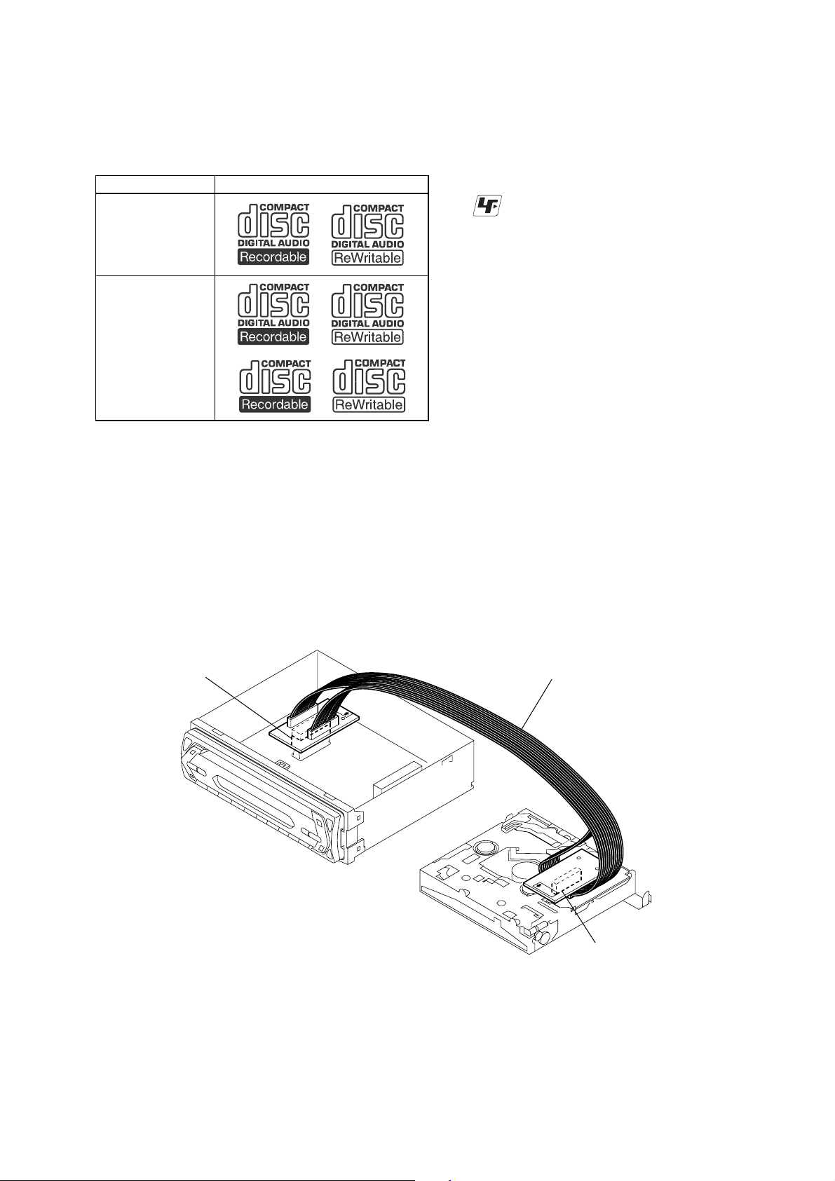
EXTENSION CABLE AND SERVICE POSITION
When repairing or servicing this set, connect the jig (extension cable)
as shown below.
UNLEADED SOLDER
•
Boards requiring use of unleaded solder are printed with the leadfree mark (LF) indicating the solder contains no lead.
(Caution: Some printed circuit boards may not come printed with
the lead free mark due to their particular size.)
: LEAD FREE MARK
Unleaded solder has the following characteristics.
• Unleaded solder melts at a temperature about 40°C higher than
ordinary solder.
Ordinary soldering irons can be used but the iron tip has to be
applied to the solder joint for a slightly longer time.
Soldering irons using a temperature regulator should be set to
about 350°C.
Caution: The printed pattern (copper foil) may peel away if the
heated tip is applied for too long, so be careful!
• Strong viscosity
Unleaded solder is more viscous (sticky, less prone to flow)
than ordinary solder so use caution not to let solder bridges
occur such as on IC pins, etc.
• Usable with ordinary solder
It is best to use only unleaded solder but unleaded solder may
also be added to ordinary solder.
• Connect the MAIN board (CNP301) and the SERVO board (CN2)
with the extension cable (Part No. J-2502-076-1).
MAIN BOARD
CNP301
J-2502-076-1
SERVO BOAR
CN2
3

CDX-S2270EE
TABLE OF CONTENTS
1. GENERAL
Location of Controls ........................................................ 5
Connections ..................................................................... 5
2. DISASSEMBLY
2-1. Sub Panel (Hex) Assy ...................................................... 8
2-2. CD Mechanism Block ..................................................... 8
2-3. Main Board ...................................................................... 9
2-4. Chassis (T) Sub Assy....................................................... 9
2-5. Roller Arm Assy .............................................................. 10
2-6. Chassis (OP) Assy ........................................................... 10
2-7. Optical Pick-up ................................................................ 11
2-8. SL Motor Assy (M902) ................................................... 11
2-9. LE Motor Assy (M903) ................................................... 12
2-10. Servo Board ..................................................................... 12
3. DIAGRAMS
3-1. Block Diagram –CD Section– ......................................... 13
3-2. Block Diagram –Main Section– ...................................... 14
3-3. Block Diagram –Key Section– ........................................ 15
3-4. Circuit Boards Location .................................................. 15
3-5. Printed Wiring Boards –CD Mechanism Section– .......... 17
3-6. Schematic Diagram –CD Mechanism Section (1/2)– ..... 18
3-7. Schematic Diagram –CD Mechanism Section (2/2)– ..... 19
3-8. Schematic Diagram –Main Section (1/3)– ...................... 20
3-9. Schematic Diagram –Main Section (2/3)– ...................... 21
3-10. Schematic Diagram –Main Section (3/3)– ...................... 22
3-11. Printed Wiring Board –Main Section– ............................ 23
3-12. Printed Wiring Board –Key Section– .............................. 24
3-13. Schematic Diagram –Key Section– ................................. 25
4. EXPLODED VIEWS
4-1. Main Section .................................................................... 33
4-2. Front Panel Section ......................................................... 34
4-3. CD Mechanism Section (1) ............................................. 35
4-4. CD Mechanism Section (2) ............................................. 36
4-5. CD Mechanism Section (3) ............................................. 37
4-6. CD Mechanism Section (4) ............................................. 38
5. ELECTRICAL PARTS LIST .................................. 39
4
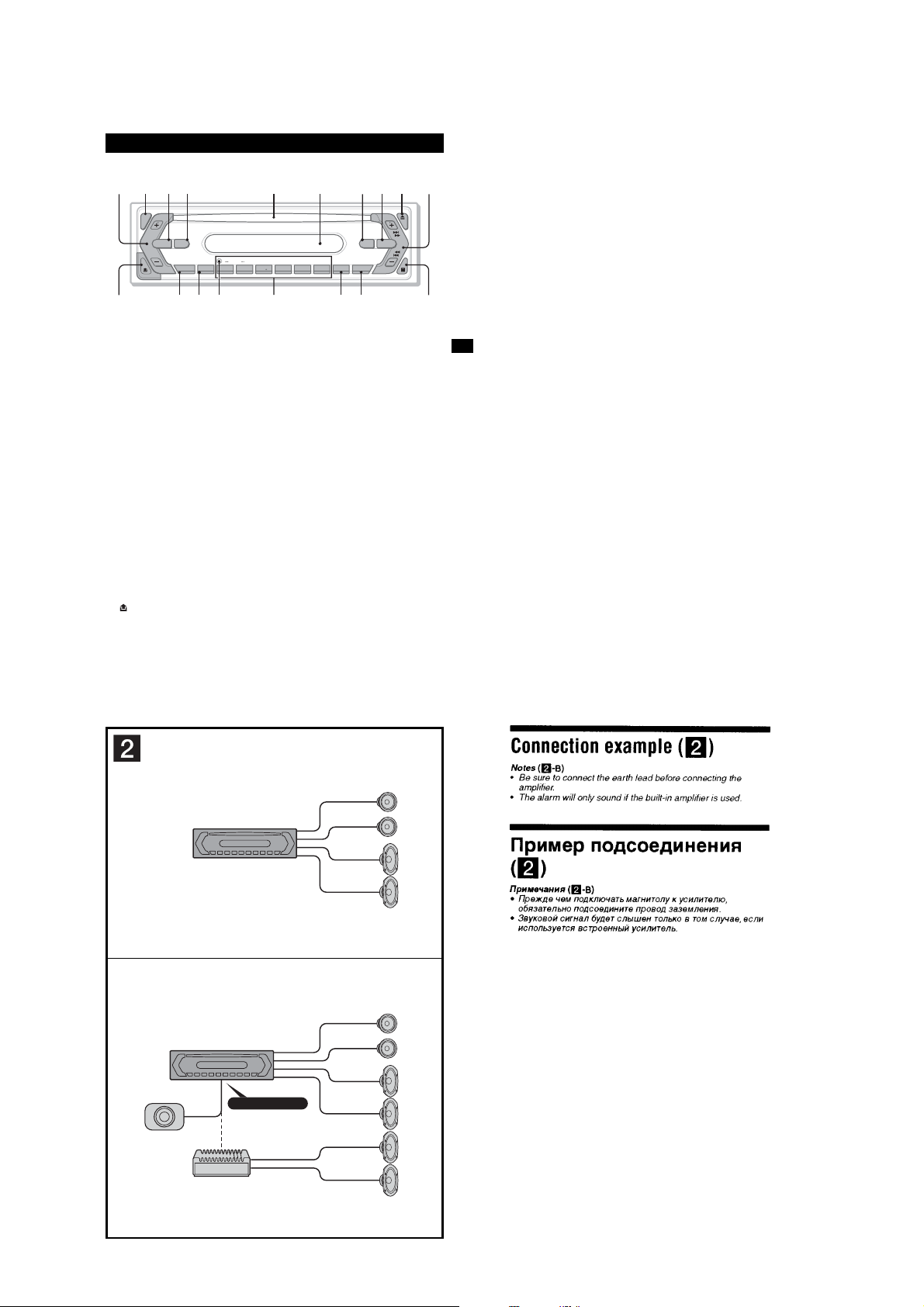
• LOCATION OF CONTROLS
q
qsq
q
qhq
q
q
Location of controls and basic operations
Main unit
1234 5 6 7890
SEL
SEEK
j
EQ3ATT
CDX-S2270EE
CDX-S2250EE
SOURCE
MODE
DIM
–+
GROUP
SENS BTM OFFDSPL 1 2 3 4 5 6
a
Refer to the pages listed for details.
a Volu me +/– button
To adjust volume.
b SEL (select) button 4, 7
To select items.
c SOURCE button
To power on/change th e source (Radio/CD).
d MODE button 6
To select the r adio band (FM/AM).
e Disc slot
Insert the disc (label side up ), playback
starts.
f Display window
g ATT (attenuate) butto n
To attenuate the sound. To cancel, pres s
again.
h EQ3 (equalizer) button 7
To select an equ alizer type (XPLOD,
VOCAL, CL UB, JAZZ, NEW AGE, ROCK,
CUSTOM or OFF).
i Z (eject) button
To eject the disc.
j SEEK +/– button
Radio:
To tune in sta tions automatically (press); find
a station manually (press an d hold).
CD:
To skip tracks (press); skip tracks
continuously (press, then pr ess again within
about 1 second and hold); fast -forward/
reverse a track (press and hold).
k (front panel release) butt on 4
d
f
SHUFREP
g
l DSPL (display)/DIM (dimmer) button
4
To change disp lay items (press); change the
display brightness (press and hold).
m SENS button
To improve weak rece ption: LOCAL/
MONO.
n RESET button (located behind the front
panel) 4
o Number buttons
Radio:
To receive stored stations (press); store
stations (press and hold).
CD:
(1)/(2): GROUP* –/+
To skip groups (pr ess); skip groups
continuously (press and ho ld).
(3): REP 6
(4): SHUF 6
p BTM button 6
To start the BT M function (press and hold).
q OFF button
To power off/stop the so urce.
r Receptor for th e card remote
commander 8
*
When an MP3/ATRAC CD is played.
CDX-S2270EE
SECTION 1
GENERAL
k
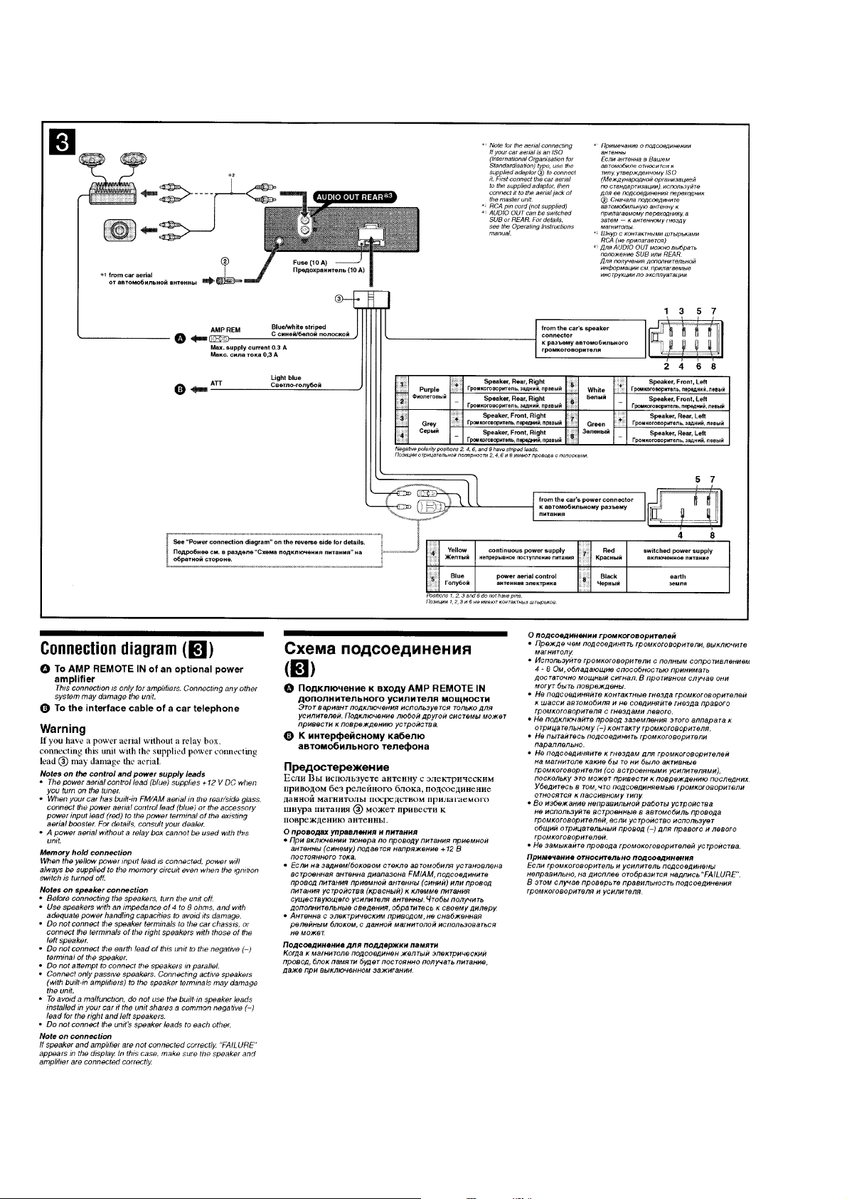
• CONNECTIONS
A
B
A
UDIO OUT REAR
5
5
CDX-S2270EE
6
SECTION 2
DISASSEMBLY
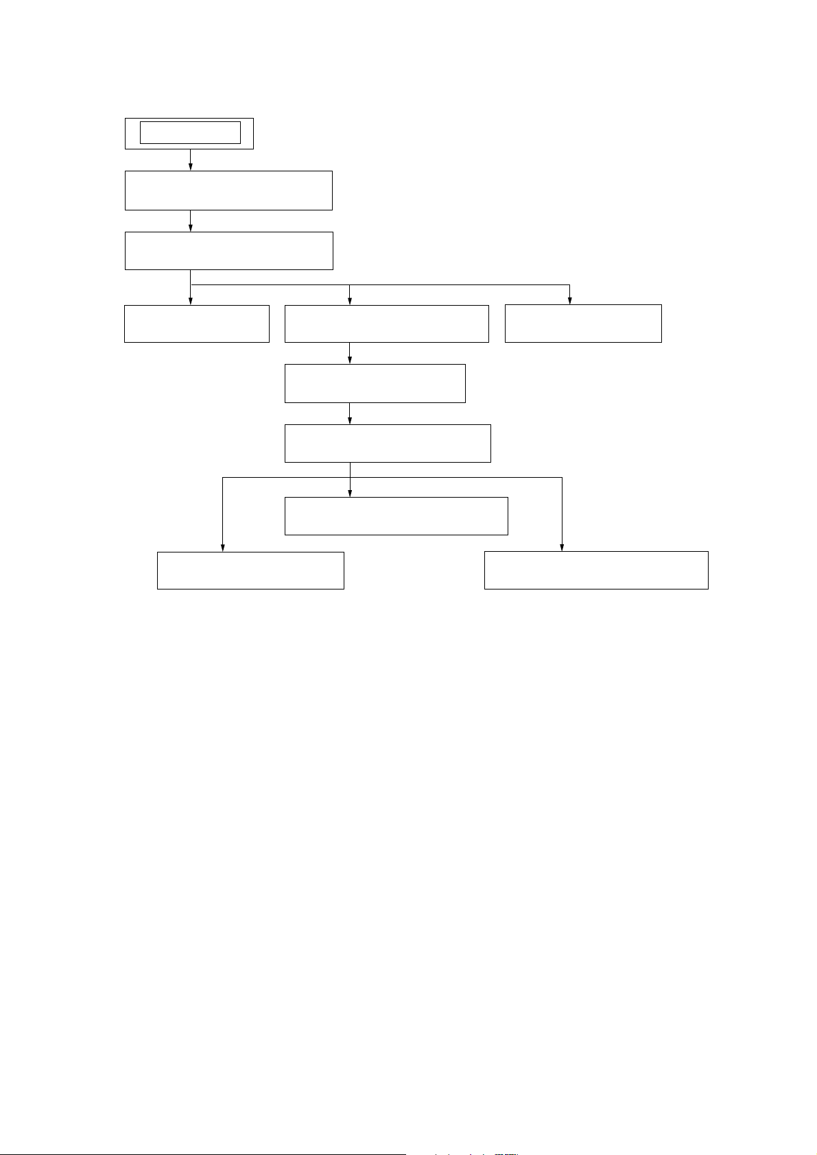
Note: This set can be disassemble according to the following sequence.
SET
2-1. SUB PANEL (HEX) ASSY
(Page 8)
2-2. CD MECHANISM BLOCK
(Page 8)
CDX-S2270EE
2-3. MAIN BOARD
(Page 9)
2-7. OPTICAL PICK-UP
(Page 11)
2-4. CHASSIS (T) SUB ASSY
(Page 9)
2-5. ROLLER ARM ASSY
(Page 10)
2-6. CHASSIS (OP) ASSY
(Page 10)
2-8. SL MOTOR ASSY (M902)
(Page 11)
2-10. SERVO BOARD
(Page 12)
2-9. LE MOTOR ASSY (M903)
(Page 12)
7
CDX-S2270EE
s
)
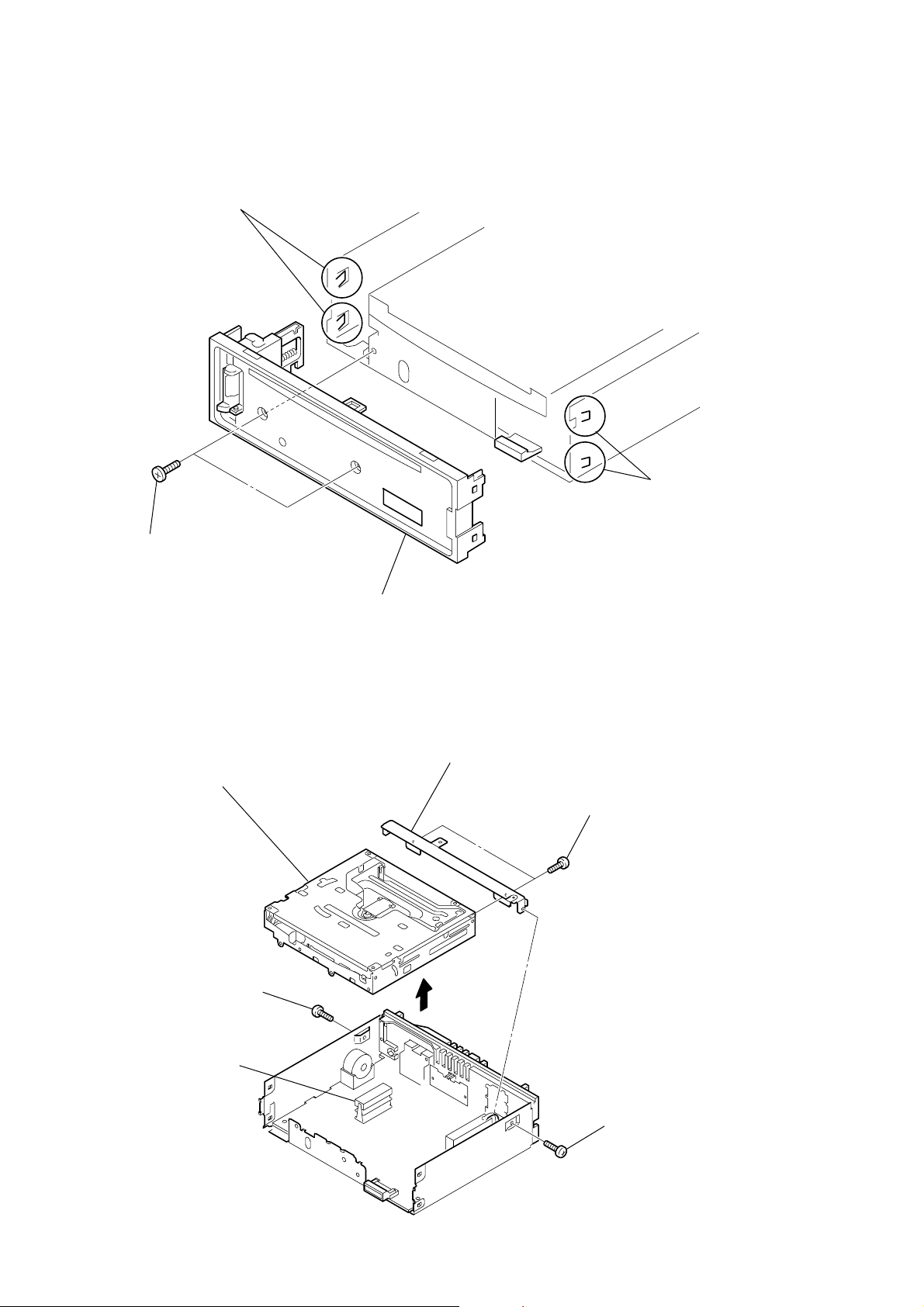
Note: Follow the disassembly procedure in the numerical order given.
2-1. SUB PANEL (HEX) ASSY
3
two claws
2
two claw
1
two
screws
(+PTT 2.6
×
6)
2-2. CD MECHANISM BLOCK
7
CD mechanism block
2
screw
(+PTT 2.6
×
6)
4
sub panel (HEX) assy
6
bracket (CD)
3
5
two
screws
(+PTT 2.6
×
4)
4
CNP301
1
screw
(+PTT 2.6
×
6
8
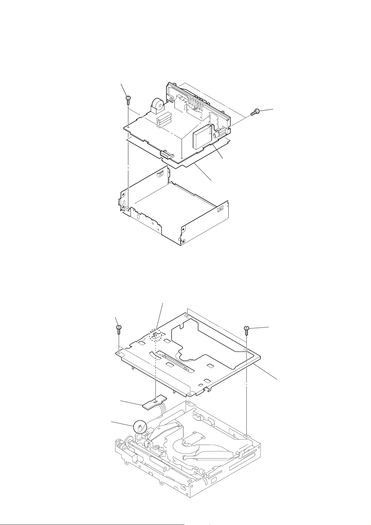
2-3. MAIN BOARD
1
three
(+BTT 2.6
screws
×
CDX-S2270EE
5)
2
two
screws
×
8)
3
MAIN board
insulating sheet
(+PTT 2.6
2-4. CHASSIS (T) SUB ASSY
2
two
screws
(+P 1.7
5
SENSOR board
3
claw
×
2.2)
4
claw
1
two
screws
×
(+P 1.7
6
2.2)
chassis (T) sub assy
9
CDX-S2270EE
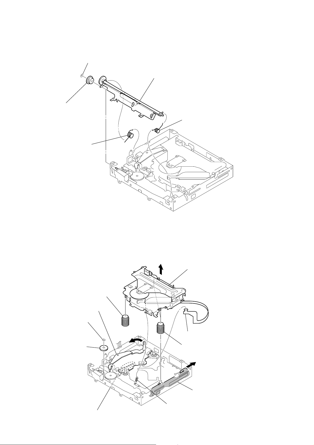
2-5. ROLLER ARM ASSY
4
gear (RA1)
1
spring (RAL)
3
washer
5
roller arm assy
2
spring (RAR)
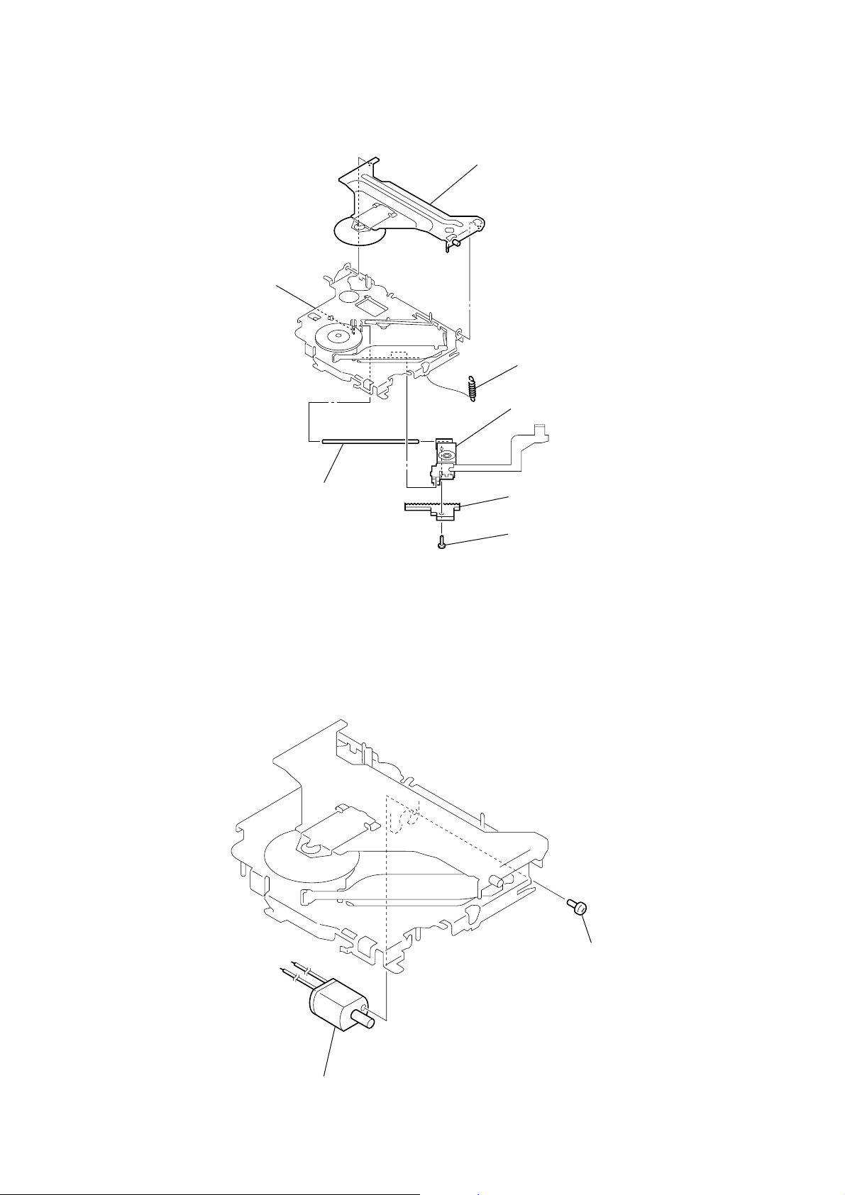
2-6. CHASSIS (OP) ASSY
0
coil spring (damper)
4
washer
5
gear (LE1)
lever (D)
6
8
qa
chassis (OP) assy
1
CN1
9
two coil springs (damper)
7
slider (R)
10
2
Remove the six solders.
3
tension spring (KF60)
2-7. OPTICAL PICK-UP
)
5
claw
2
chucking arm sub assy
1
tension coil spring (CHKG)
7
optical pick-up
CDX-S2270EE
2-8. SL MOTOR ASSY (M902)
6
main shaft
4
rack (SL)
3
screw
(+B 1.4
×
5)
2
SL motor assy (M902)
1
screw
(+P 1.4
×
1.8
11
CDX-S2270EE
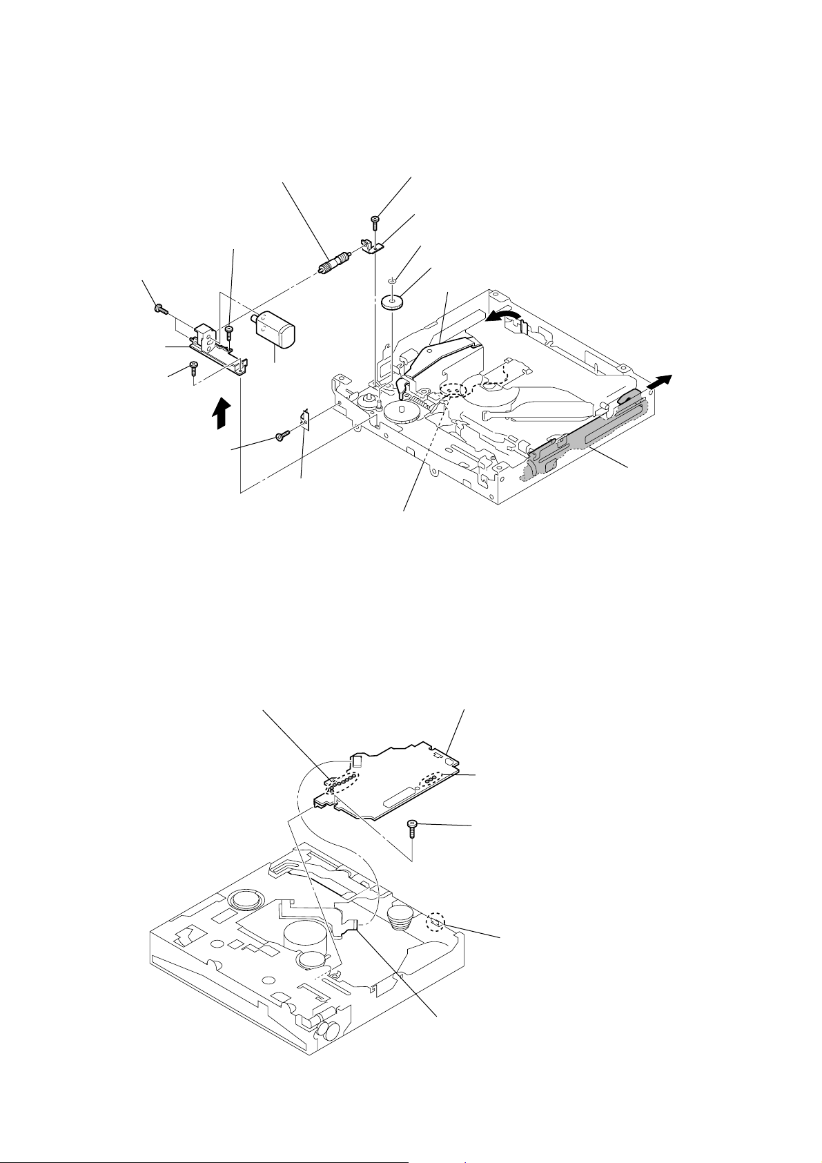
2-9. LE MOTOR ASSY (M903)
qf
two toothed lock
(+M 1.4
bracket (LEM-N)
qs
(+M 1.7
screw
×
)
2.5)
screws
qd
qa
screw
(+M 1.7
qg
(M903)
0
woam (LEB) assy
×
2.5)
LE motor assy
8
screw
(+M 1.7
9
bearing (LEB-N)
2
washer
3
gear (LE1)
lever (D)
×
2.5)
4
5
6
screw
(+P 1.7
2-10. SERVO BOARD
×
2.2)
7
leaf spring (LE)
1
Remove the eight solders.
1
Remove the two solders.
6
SERVO board
2
Remove the three solders.
4
screw
slider (R)
12
3
CN1
5
claw
SECTION 3
DIAGRAMS
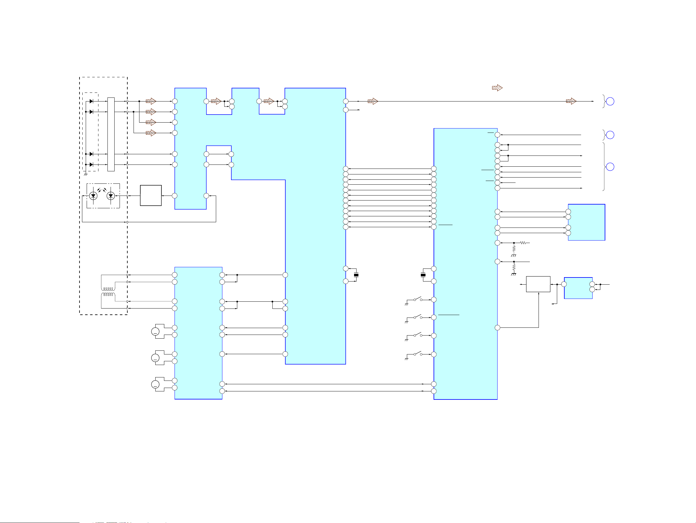
3-1. BLOCK DIAGRAM — CD SECTION —
DETECTOR
PD2
PD1
E
F
LASER DIODE
PICK-UP BLOCK
(KSS1000E)
2-AXIS DEVICE
(FOCUS)
(TRACKING)
PD LD
OPTICAL
PD2
PD1
I-V AMP
MON OUT
FCS+
FCS–
TRK+
TRK–
LD+
FPI2
96
94
97
95
E
F
AUTOMATIC
POWER
CONTROL
Q1
M902
M
(SLED)
99
98
91
FOCUS/TRACKING COIL DRIVE,
16
15
18
17
14
13
RFO
FNI2
FPI1
FNI1
RFRP
TNI
TPI
LDO
VO4–
VO4+
VO3–
VO3+
VO1+
VO1–
TEI
MDI
SLED/SPINDLE/LOADING
MOTOR DRIVE
IC1
87
3
6
92
OPIN4–
OPOUT4
OPIN3–
OPOUT3
OPOUT1
OPIN2
CDX-S2270EE
• R-ch is omitted due to same as L-ch.
• Signal Path
: CD PLAY
79
RFEQO
85
AGCI
86
RFDCI
DIGITAL SERVO,
DIGITAL SIGNAL PROCESSOR
RFZI
1
TEZI
7
26
25
23
22
4
7
IC2
77
78
9
10
46
12
13
RFI
RFRPI
F0O
TRO
IO0(/HSO)
FMO
DMO
MUTE
REQ
STBY
ZDET
/RST
/CCE
BUCK
BUS3
BUS2
BUS1
BUS0
SBSY
SYS RST
UNI SI
UNI SO
UNI CLK
BUS ON
B/U CHECK
ATT
IC501 (1/3)
VDD
CE
CD-L
15
3
30
LO
27
RO
XI
XO
R-CH
RST
75
UNISI
56
RXD
25
UNISO
57
TXD
26
UNICKI
DEC_XMUTE
56
53
43
18
42
41
40
39
38
37
36
14
23
24
X2
16.934MHz
SW1
(DOWN)
SW2
(SELF)
SW3
(DISC IN)
X1
12MHz
37
DEC_INT
30
DEC_SSTBY
27
CD_ZDET
15
CD_XRST
14
CD_XCCE
13
CD_BUCK
12
CD_BUS3
11
CD_BUS2
10
CD_BUS1
8
CD_BUS0
7
CD_SBSY
52
X1
81
X0
80
MEC_DSW
46
MEC_SELFSW
53
MEC_INSW
45
XFLASH&EJECT_OK
CD
SYSTEM CONTROL
IC3
MECON_CHK
CDON_CHK
BUS_ON
BU_IN
RSTX
A_ATT
OPEN_REQ
CDON
ZMUTE
58
50
51
75
60
61
62
64
66
67
68
NC
1
+1.5V
1.5V_ON
BU+3.3V
MECHA+6V
SERVO+3.3V
+1.5V ON/OFF
SWITCH
Q2,3
+1.5V
SYSTEM CONTROL
EJECT_OK_SW
89
OPEN REQ
54
CD_ON
98
CD_MUTE-R
93
+1.5V REG
IC6
VOUT
MAIN
A
SECTION
(Page 14)
DISPLAY
C
SECTION
(Page 15)
MAIN
B
SECTION
(Page 14)
BU+3.3V
CDX-S2270EE
M901
(SPINDLE)
M903
(LOADING)
MUTE
FWD
REV
21
1
28
12
M
M
VO2+
11
VO2–
10
VOL+
9
VOL–
IO1(/UHSO)
47
SW4
(LIMIT)
MEC_LIMIT
42
MEC_LOAD
43
MEC_EJECT
44
13 13
CDX-S2270EE
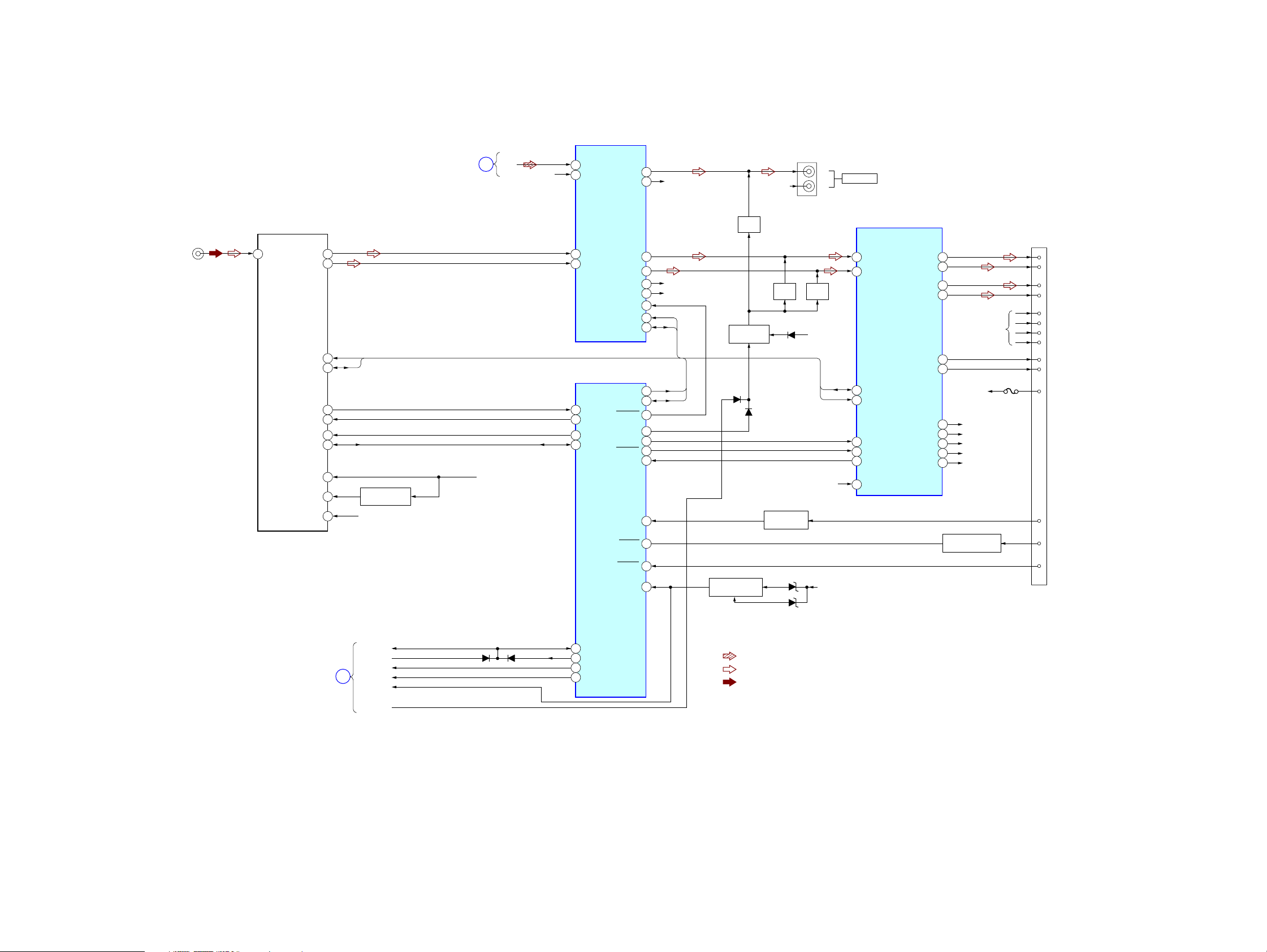
3-2. BLOCK DIAGRAM — MAIN SECTION —
ELECTRONIC VOLUME
IC401
J1
(ANTENNA)
1
ANT
TU1
(TUNER UNIT)
TU-SCL
TU-SDA
S-METER
TU-MUTE
E2P-SCL
E2P-SDA
TU-VDD(TU5V)
E2P-VDD
L-CH
R-CH
VCC
CD
SECTION
(Page 13)
4
3
SCL
13
SDA
14
6
7
16
17
10
11
15
TUNER +5V REG.
Q1
BU+3.3V
CD-L
A
AUDIO+8.3V
R-CH
9
CD LCH
8
CD RCH
7
TU-LCH
6
TU-RCH
SYSTEM CONTROL
IC501 (2/3)
39
VSM
12
TUATT
25
EEP CKO
24
EEP SIO
OUT SUB-L
OUT SUB-R
OUT-FL
OUT-RL
OUT-FR
OUT-RR
MUTE
SCL
SDA
I2C CKO
I2C SIO
VOL ATT
ATT
BEEP
AMPSTB
DIAG
TEL ATT
ACC_IN
TEST IN
BU IN
17
18
23
22
25
24
29
30
31
33
34
9
86
5
26
8
74
72
73
54
R-CH
R-CH (FRONT)
R-CH (REAR)
SCL
SDA
SCL
SDA
MUTE
Q481
MUTE DRIVE
Q478,479
BATTERY CHECK
Q580-582
D511
ATTENUATION
R-CH
MUTE
Q441
Q651
D479
D580
MUTE
Q461
BATT
L
R
SDA
SCL
BATT
BATT
J330
AUDIO OUT
12
IN-FL
11
IN-RL
2
SDA
4
SCL
16
BEEP
22
STB
25
DIAG
35
VP
POWER AMP,
POWER SUPPLY
IC750
OUT-FL+
OUT-RL+
OUT-RL-
AMP-REM
ANT-REM
AUDIO8.3V
SERVO3.3V
MECHA6V
PANEL+B
OUT-FL-
B.UP+B
5
3
9
7
29
27
BATT
30
AUDIO+8.3V
37
BU+3.3V
31
SERVO+3.3V
33
MECHA+6V
34
PANEL+B
ACCESSORY CHECK
Q631
R-CH
F901
CN601
10
12
11
16
13
15
1
FL+
9
FL-
2
RL+
RL-
4
FR+
FR-
3
RR+
RR-
5
AMPREM
6
ANTREM
TEL-MUTE
7
ACC
TEST
CDX-S2270EE
CD
SECTION
(Page 13)
B
UNI SI
UNI SO
UNI CLK
BUS ON
B/U CHECK
ATT
D512
58
59
60
87
UNI SI
UNI SO
UNI SCK
BUS ON
D581
• R-CH is omitted due to same as L-CH.
• Signal Path
: CD PLAY
: FM
: MW/LW
1414
 Loading...