

Page 1
CDX-R3000/R3000T
SERVICE MANUAL
Ver 1.0 2003. 12
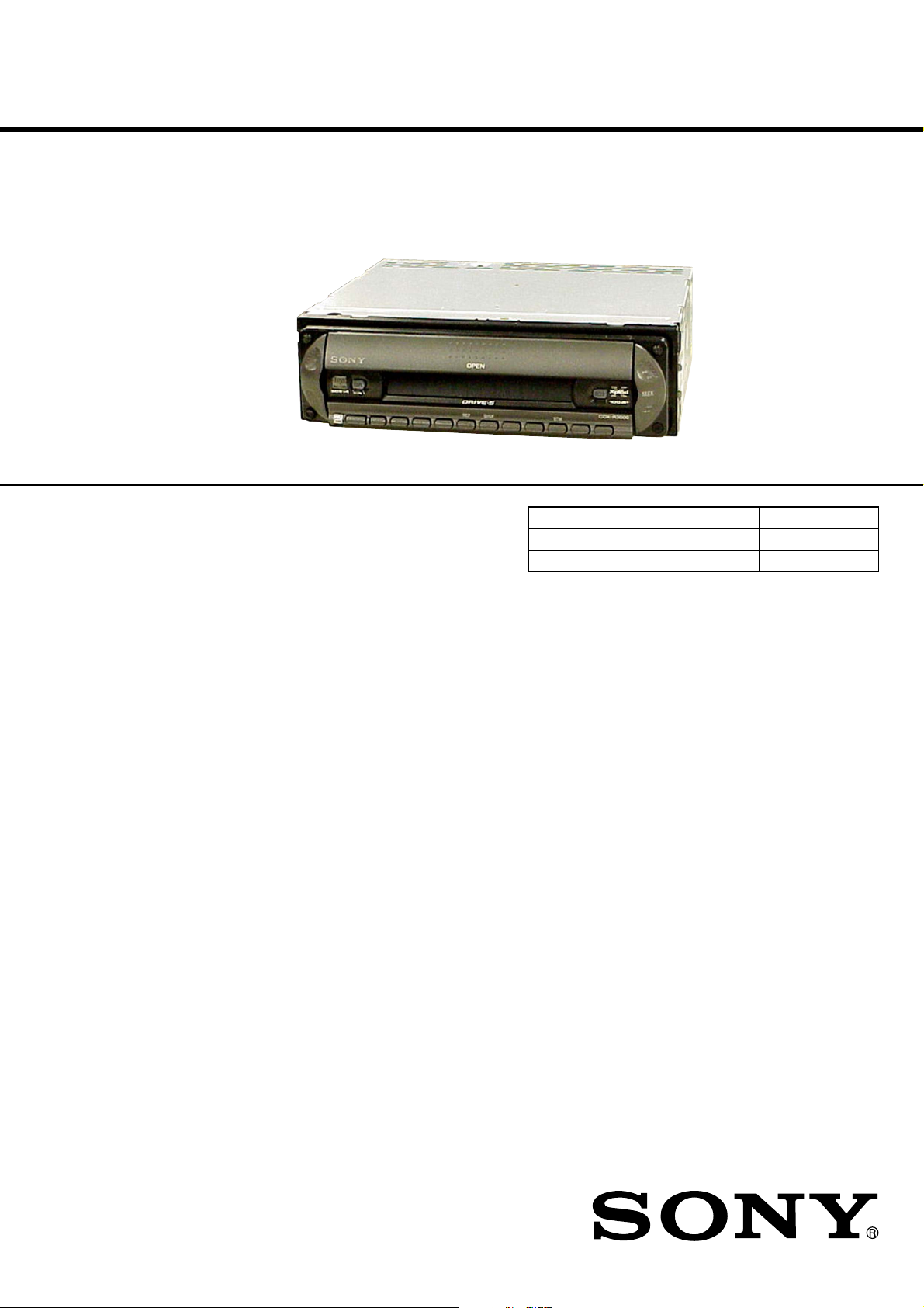
Photo: CDX-R3000
• The tuner and CD sections have no adjustments.
SPECIFICATIONS
AEP Model
UK Model
CDX-R3000
E Model
CDX-R3000T
Model Name Using Similar Mechanism NEW
CD Drive Mechanism Type MG-611XA-186//Q
Optical Pick-up Name KSS1000E
CD player section
Signal-to-noise ratio 120 dB
Frequency response 10 – 20,000 Hz
Wow and flutter Below measurable limit
Tuner section
FM
Tuning range 87.5 – 108.0 MHz
Aerial terminal External aerial connector
Intermediate frequency 10.7 MHz/450 kHz
Usable sensitivity 9 dBf
Selectivity 75 dB at 400 kHz
Signal-to-noise ratio 67 dB (stereo),
69 dB (mono)
Harmonic distortion at 1 kHz
0.5% (stereo),
0.3% (mono)
Separation 35 dB at 1 kHz
Frequency response 30 – 15,000 Hz
MW/LW (CDX-R3000)
Tuning range MW: 531 – 1,602 kHz
LW: 153 – 279 kHz
Aerial terminal External aerial connector
Intermediate frequency 10.7 MHz/450 kHz
Sensitivity MW: 30 µV
LW: 40 µV
AM (CDX-R3000T)
Tuning range 531 – 1,602 kHz
Aerial terminal External aerial connector
Intermediate frequency 10.7 MHz/450 kHz
Sensitivity AM: 30 µV
Power amplifier section
Outputs Speaker outputs
(sure seal connectors)
Speaker impedance 4 – 8 ohms
Maximum power output 50 W × 4 (at 4 ohms) (CDX-R3000)
52 W × 4 (at 4 ohms) (CDX-R3000T)
General
Outputs Audio outputs terminal
(rear/sub switchable)
Power aerial relay control terminal
Power amplifier control terminal
Inputs Telephone ATT control terminal (CDX-R3000)
Remote controller input terminal
Aerial input terminal
Tone controls Low: ±10 dB at 60 Hz (XPLOD)
Mid: ±10 dB at 1 kHz (XPLOD)
High: ±10 dB at 10 kHz (XPLOD)
– Continued on next page –
FM/MW/LW COMPACT DISC PLAYER
CDX-R3000
9-961-414-01
2003L04-1
© 2003. 12
FM/AM COMPACT DISC PLAYER
CDX-R3000T
Sony Corporation
e Vehicle Company
Published by Sony Engineering Corporation
1
Page 2
CDX-R3000/R3000T
Power requirements 12 V DC car battery
(negative ground)
Dimensions Approx. 178 × 50 × 179 mm
(w/h/d)
Mounting dimensions Approx. 182 × 53 × 161 mm
(w/h/d)
Mass Approx. 1.2 kg
Supplied accessories Parts for installation and connections (1 set)
Front panel case (1)
Design and specifications are subject to change without
notice.
SERVICE NOTES
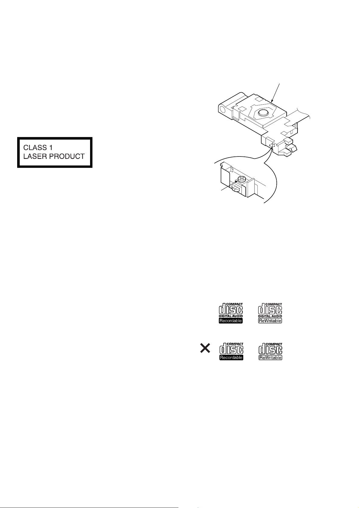
This label is located on the bottom of the chassis.
NOTES ON HANDLING THE OPTICAL PICK-UP BLOCK
OR BASE UNIT
The laser diode in the optical pick-up block may suffer electrostatic
breakdown because of the potential difference generated by the
charged electrostatic load, etc. on clothing and the human body.
During repair, pay attention to electrostatic breakdown and also use
the procedure in the printed matter which is included in the repair
parts.
The flexible board is easily damaged and should be handled with
care.
NOTES ON LASER DIODE EMISSION CHECK
The laser beam on this model is concentrated so as to be focused on
the disc reflective surface by the objective lens in the optical pickup block. Therefore, when checking the laser diode emission, observe from more than 30 cm away from the objective lens.
Notes on Chip Component Replacement
• Never reuse a disconnected chip component.
• Notice that the minus side of a tantalum capacitor may be dam-
aged by heat.
If the optical pick-up block is defective, please replace the whole
optical pick-up block.
Never turn the semi-fixed resistor located at the side of optical
pick-up block.
optical pick-up
semi-fixed resistor
TEST DISCS
This set can playback CD-R and CD-ROM discs. The following
test discs should be used to check the capability:
CD-R test disc TCD-R082LMT (Part No. J-2502-063-1)
CD-RW test disc TCD-W082L (Part No. J-2502-063-2)
Notes on CD-R/CD-RW discs
•You can play CD-Rs (recordable CDs)/CD-RWs (re writable CDs)
designed for audio use on this unit.
Look for these marks to distinguish CD-Rs/CD-RWs for audio
use.
These marks denote that a disc is not for audio use.
SAFETY-RELATED COMPONENT WARNING!!
COMPONENTS IDENTIFIED BY MARK 0 OR DOTTED LINE
WITH MARK 0 ON THE SCHEMATIC DIAGRAMS AND IN
THE PARTS LIST ARE CRITICAL TO SAFE OPERATION.
REPLACE THESE COMPONENTS WITH SONY P ARTS WHOSE
PART NUMBERS APPEAR AS SHOWN IN THIS MANUAL OR
IN SUPPLEMENTS PUBLISHED BY SONY.
2
• Some CD-Rs/CD-RWs (depending on the equipment used for
its recording or the condition of the disc) may not play on this
unit.
•You cannot play a CD-R/a CD-RW that is not finalized*.
*A process necessary for a recorded CD-R/CD-RW disc to be
played on the audio CD player.
Page 3
z
D
UNLEADED SOLDER
Boards requiring use of unleaded solder are printed with the lead
free mark (LF) indicating the solder contains no lead.
(Caution: Some printed circuit boards may not come printed with
the lead free mark due to their particular size.)
: LEAD FREE MARK
Unleaded solder has the following characteristics.
• Unleaded solder melts at a temperature about 40°C higher than
ordinary solder.
Ordinary soldering irons can be used but the iron tip has to be
applied to the solder joint for a slightly longer time.
Soldering irons using a temperature regulator should be set to
about 350°C.
Caution: The printed pattern (copper foil) may peel away if the
heated tip is applied for too long, so be careful!
• Strong viscosity
Unleaded solder is more viscous (sticky, less prone to flow)
than ordinary solder so use caution not to let solder bridges
occur such as on IC pins, etc.
• Usable with ordinary solder
It is best to use only unleaded solder but unleaded solder may
also be added to ordinary solder.
CDX-R3000/R3000T
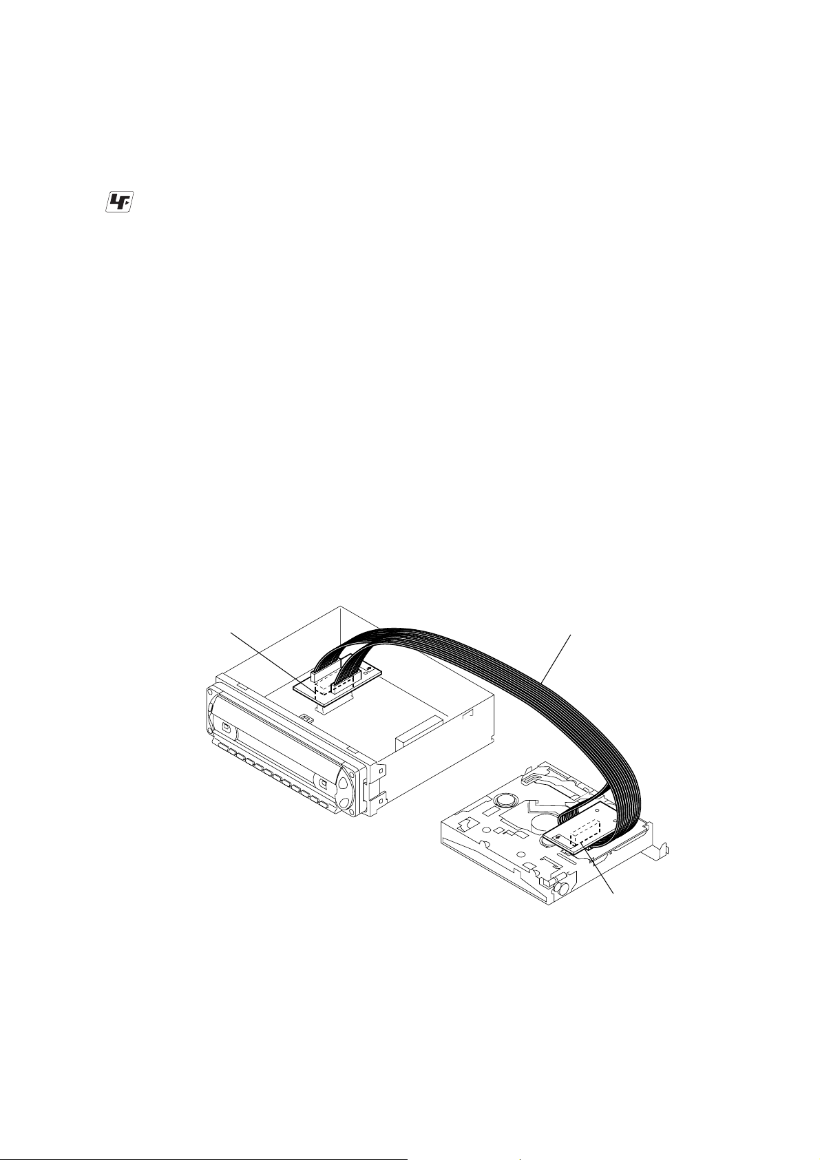
EXTENSION CABLE AND SERVICE POSITION
When repairing or servicing this set, connect the jig (extension cable)
as shown below.
• Connect the MAIN board (CNP301) and the SER V O board (CN1)
with the extension cable (Part No. J-2502-076-1).
MAIN BOARD
CNP301
J-2502-076-1
SERVO BOAR
CN1
3
Page 4

CDX-R3000/R3000T
TABLE OF CONTENTS
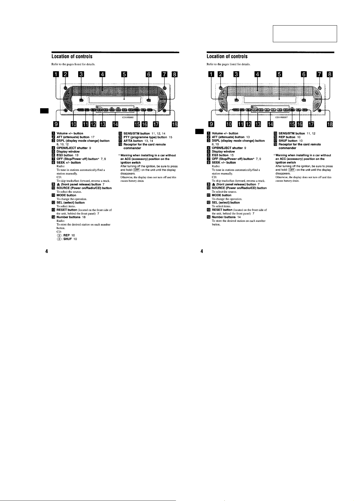
1. GENERAL
Location of controls................................................................. 5
Connections ............................................................................. 6
2. DISASSEMBLY
2-1. Sub Panel Assy.................................................................... 8
2-2. CD Mechanism Block ......................................................... 9
2-3. Main Board ......................................................................... 9
2-4. Chassis (T) Sub Assy ........................................................ 10
2-5. Roller Arm Assy................................................................ 10
2-6. Chassis (OP) Assy............................................................. 11
2-7. Optical Pick-up ................................................................. 11
2-8. SL Motor Assy (M902) .....................................................12
2-9. LE Motor Assy (M903)..................................................... 12
2-10. Servo Board....................................................................... 13
3. DIAGRAMS
3-1. IC Pin Descriptions ........................................................... 14
3-2. Block Diagram –CD Section–........................................... 19
3-3. Block Diagram –Tuner Section–....................................... 20
3-4. Block Diagram –Display Section–.................................... 21
3-5. Printed Wiring Boards –CD Mechanism Section–............ 22
3-6. Schematic Diagram –CD Mechanism Section– ................23
3-7. Printed Wiring Board –Main Section– .............................. 24
3-8. Schematic Diagram –Main Section (1/2)– ........................25
3-9. Schematic Diagram –Main Section (2/2)– ........................26
3-10. Printed Wiring Board –Key Section– ................................ 27
3-11. Schematic Diagram –Key Section–...................................28
3-12. IC Block Diagrams............................................................ 29
4. EXPLODED VIEWS
4-1. Main Section ..................................................................... 32
4-2. Front Panel Section ........................................................... 33
4-3. CD Mechanism Section (1) ...............................................34
4-4. CD Mechanism Section (2) ...............................................35
4-5. CD Mechanism Section (3) ...............................................36
4-6. CD Mechanism Section (4) ...............................................37
5. ELECTRICAL PARTS LIST ........................................ 38
4
Page 5
CDX-R3000/R3000T
SECTION 1
GENERAL
(CDX-R3000) (CDX-R3000T)
This section is extracted
from instruction manual.
5
Page 6
CDX-R3000/R3000T
Connections (CDX-R3000)
6
Page 7
Connections (CDX-R3000T)
CDX-R3000/R3000T
7
Page 8
CDX-R3000/R3000T
s
SECTION 2
DISASSEMBLY
Note : This set can be disassemble according to the following sequence.
SET
2-1. SUB PANEL ASSY
(Page 8)
2-2. CD MECHANISM BLOCK
(Page 9)
2-3. MAIN BOARD
(Page 9)
2-4. CHASSIS (T) SUB ASSY
(Page 10)
2-5. ROLLER ARM ASSY
(Page 10)
2-6. CHASSIS (OP) ASSY
(Page 11)
2-8. SL MOTOR ASSY (M902)
(Page 12)
2-7. OPTICAL PICK-UP
(Page 11)
Note : Follow the disassembly procedure in the numerical order given.
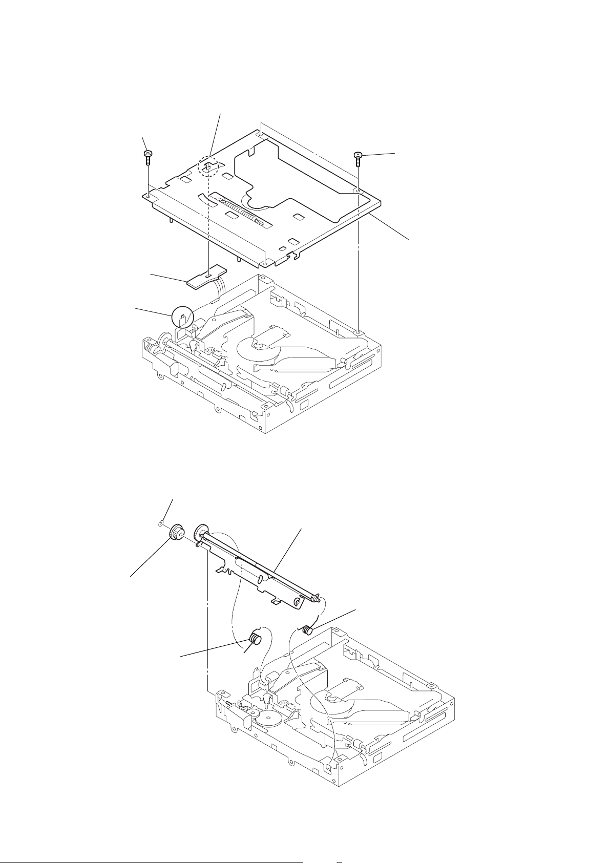
2-1. SUB PANEL ASSY
2-10. SERVO BOARD
(Page 13)
2-9. LE MOTOR ASSY (M903)
(Page 12)
3
two claws
2
two claw
1
two
screws
(+PTT 2.6
x
6)
4
sub panel assy
8
Page 9
2-2. CD MECHANISM BLOCK
)
)
5
CD mechanism block
2
screw
(+PTT 2.6
x
CDX-R3000/R3000T
7
bracket (CD)
8
shield sheet
6
two
screws
x
(+PTT 2.6
3
6)
4)
2-3. MAIN BOARD
1
three ground point screws
(+PTT 2.6
x
6)
4
CNP301
3
MAIN board
1
screw
(+PTT 2.6
2
two
screws
(+PTT 2.6
x
x
6
6
9
Page 10
CDX-R3000/R3000T
2-4. CHASSIS (T) SUB ASSY
2
two
screws
x
(+P 1.7
5
SENSOR board
3
claw
2.2)
4
claw
1
two
screws
(+P 1.7
x
2.2)
6
chassis (T) sub assy
2-5. ROLLER ARM ASSY
4
worm wheel (RA)
1
spring (RAL)
3
washer
5
roller arm assy
2
spring (RAR)
10
Page 11
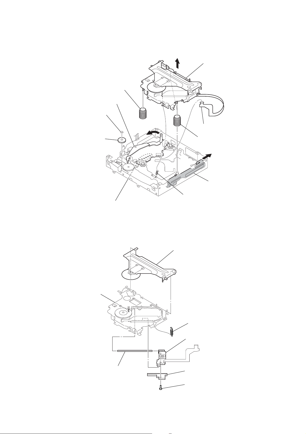
2-6. CHASSIS (OP) ASSY
)
0
coil spring (damper)
4
washer
5
gear (LE1)
lever (D)
6
8
CDX-R3000/R3000T
qa
chassis (OP) assy
1
CN2
9
two coil springs (damper)
7
2-7. OPTICAL PICK-UP
5
claw
2
Remove the six solderings.
3
tension coil spring (KF)
2
chucking arm sub assy
1
tension coil spring (CHKG
slider (R)
6
main shaft
7
optical pick-up
4
rack (SL)
3
screw
x
(+B 1.4
5)
11
Page 12
CDX-R3000/R3000T
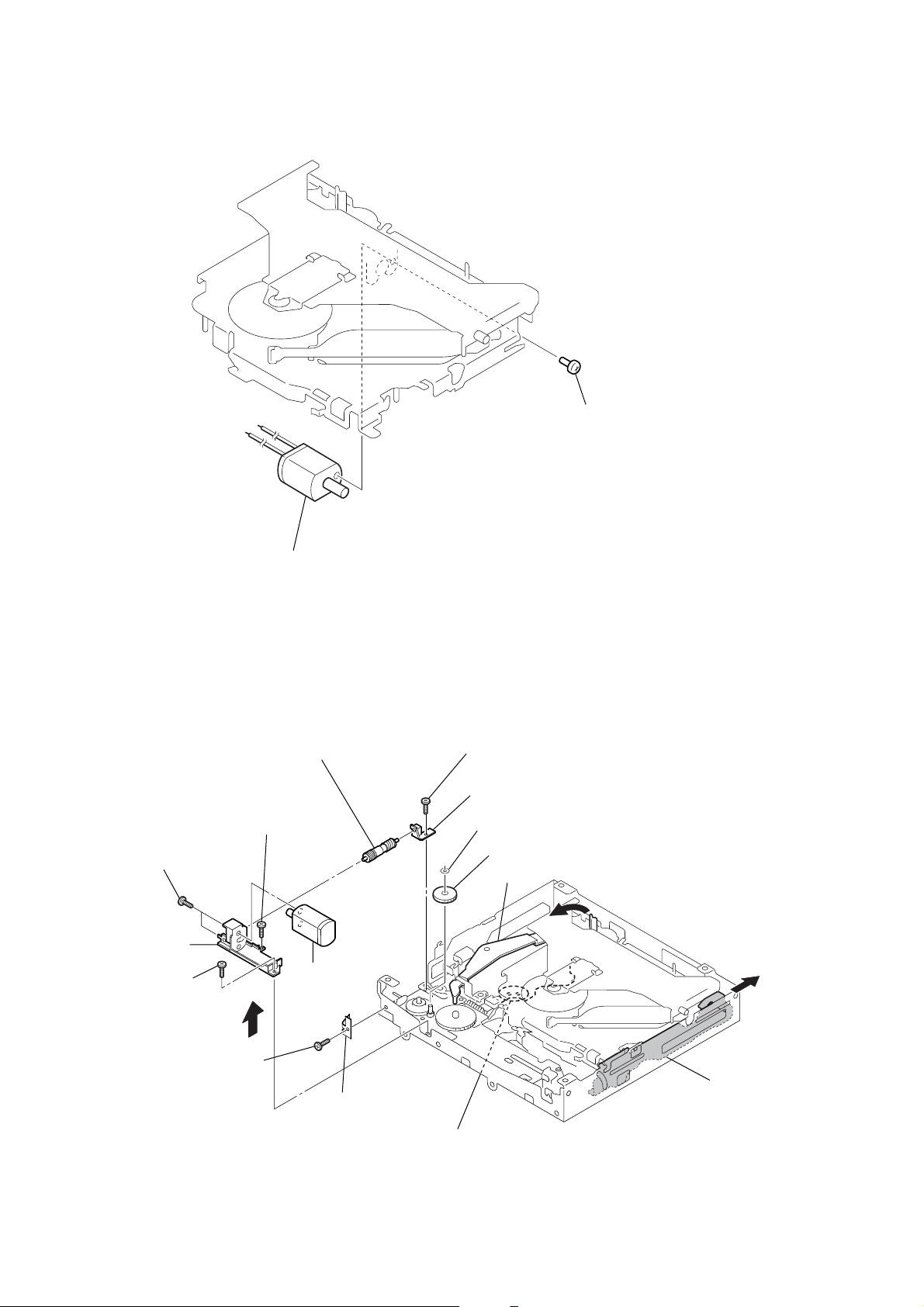
2-8. SL MOTOR ASSY (M902)
1
screw
(+P 1.4
x
1.8)
2-9. LE MOTOR ASSY (M903)
qf
two toothed lock
(+M 1.4
bracket (LEM)
qs
(+M 1.7
screw
x
)
screws
2.5)
qa
screw
(+M 1.7
qd
2
SL motor assy (M902)
0
woam (LEB) assy
x
2.5)
qg
LE motor assy
(M903)
8
screw
(+M 1.7
9
bearing (LEB)
2
washer
gear (LE1)
3
lever (D)
x
2.5)
4
5
12
6
screw
(+P 1.7
x
2.2)
7
leaf spring (LE)
1
Remove the soldering.
slider (R)
Page 13
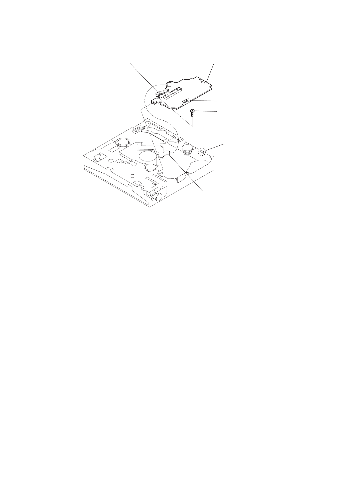
2-10. SERVO BOARD
1
Remove the eight solderings.
CDX-R3000/R3000T
6
SERVO board
2
Remove the three solderings.
4
toothed lock
(M 1.7)
5
claw
screw
3
CN2
13
Page 14
CDX-R3000/R3000T
SECTION 3
DIAGRAMS
3-1. IC PIN DESCRIPTIONS
• IC1 µPD63712GC-8EU-A (RF AMP, DIGITAL SERVO, DIGITAL SIGNAL PROCESSOR) (SERVO BOARD)
Pin No. Pin Name I/O Pin Description
1LDOLaser diode ON/OFF control signal output (L: laser OFF, H: laser ON)
2PDIDimmer monitor input from optical pick-up laser diode.
3PNINot used. (Fixed at L in this set)
4AVDD — Analog power supply pin (+3.3 V)
5 DGND — Ground
6 RFOK O RFOK signal output to system control IC.
7 INTQ O CD text pack synchronization signal output to system control IC.
8 RST I CD reset signal input from system control IC.
9A0I
10 STB I Data strobe signal input from system control IC.
11 SCK I Serial clock input from system control IC.
12 SO O Serial data output to system control IC.
13 SI I Serial data input from system control IC.
14 DVDD — Power supply pin (+3.3 V)
15 DAVDD — D/A converter power supply (+) pin (+3.3 V)
16 ROUT O Analog audio signal output (R-ch)
17 DAGND — Ground
18 REGC — Capacitor connection pin for SCF regulator.
19 DAGND — Ground
20 LOUT O Analog audio signal output (L-ch)
21 DAVDD — D/A converter power supply (+) pin (+3.3 V)
22 XVDD — Power supply pin (+3.3 V)
23 XTAL O Main system clock output (16.9344 MHz)
24 XTAL I Main system clock input (16.9344 MHz)
25 XGND — Ground
26 DVDD — Power supply pin (+3.3 V)
27 C1D1/FZD O Not used. (Open)
28 C1D2/TZD O Not used. (Open)
29 C2D1/RMUTE O CD R-ch data zero detection signal output
30 C2D2/LMUTE O CD L-ch data zero detection signal output
31 C2D3/SHOCK/SBSY O Not used. (Open)
32 LOCK/FR O Not used. (Open)
33 WFCK/MIRR O Not used. (Open)
34 RFCK/HOLD O Not used. (Open)
35 PLCK O Not used. (Open)
36 C16M O Not used. (Open)
37 DGND — Ground
38 TX O Not used. (Open)
39 EMPH/RAMOVER O Not used. (Open)
40 FLAG O Not used. (Open)
41 DVDD — Power supply pin (+3.3 V)
42 LIMIT I Not used. (Fixed at L in this set)
43 XTALEN I
44 DGND — Ground
45 DIN I Not used. (Connect to DOUT in this set)
46 DOUT O Not used. (Connect to DIN in this set)
47 SCKIN I Not used. (Connect to SCKO in this set)
48 SCKO O Not used. (Connect to SCKIN in this set)
49 LRCKIN I Not used. (Connect to LRCK in this set)
Command/parameter discrimination signal input from system control IC.
(L: command transmission, H: parameter transmission)
Oscillation circuit ON/OFF control signal input (L: ON, H: OFF)
(Fixed at L in this set)
14
Page 15

Pin No. Pin Name I/O Pin Description
50 LRCK O Not used. (Connect to LRCKIN in this set)
51 DVDD — Power supply pin (+3.3 V)
52 FD+ O Focus servo drive PWM signal output (+)
53 FD– O Focus servo drive PWM signal output (–)
54 TD+ O Tracking servo drive PWM signal output (+)
55 TD– O Tracking servo drive PWM signal output (–)
56 SD+ O Sled servo drive PWM signal output (+)
57 SD– O Sled servo drive PWM signal output (–)
58 MD+ O Spindle servo drive PWM signal output (+)
59 MD– O Spindle servo drive PWM signal output (–)
60 DGND — Ground
61 TESTEN I Test setting input (Fixed at L in this set)
62 to 66 TEST4 to TEST0 I Test setting input (Fixed at L in this set)
67 ADGND — A/D converter power supply (–) pin
68 EFM O EFM signal output
69 ASY I EFM comparator reference voltage input
70 ADVDD — A/D converter power supply pin (+3.3 V)
71 RFI I RF signal input for EFM data growing.
72 EQ2 — Not used. (Open)
73 EQ1 — RF amplifier equalizer parts connection pin
74 RF– I Not used. (Open)
75 RF2– I RF amplifier inversion input
76 AGCO O RF signal output after on AGC.
77 AGCI I RF AGC signal amplifier input
78 RFO O RF signal output before on AGC.
79 ATEST I Not used. (Open)
80 C3T — Capacitor connection pin for 3T detection.
81 AGND — Ground
82 A I Signal input (A) from optical pick-up detector.
83 C I Signal input (C) from optical pick-up detector.
84 B I Signal input (B) from optical pick-up detector.
85 D I Signal input (D) from optical pick-up detector.
86 F I Signal input (F) from optical pick-up detector.
87 E I Signal input (E) from optical pick-up detector.
88 VREFIN I Reference voltage (+1.65 V) input
89 AVDD — Analog power supply pin (+3.3 V)
90 REFOUT O Reference voltage (+1.65 V) output
91 REFC — Capacitor connection pin for reference voltage output.
92 FE– I Focus error signal amplifier inversion input
93 FEO O Focus error signal amplifier output
94 ADCIN I Not used. (Open)
95 TE– I Tracking error signal amplifier inversion input
96 TEO O Tracking error signal amplifier before output
97 TE2 O Tracking error signal amplifier after output
98 TEC I Tracking error signal comparator input
99 AGND — Ground
100 PWMSW I Not used. (Fixed at L in this set)
CDX-R3000/R3000T
15
Page 16

CDX-R3000/R3000T
• IC501 MN101E01KDD (SYSTEM CONTROL) (MAIN BOARD (2/2))
Pin No. Pin Name I/O Pin Description
1DAVDD — D/A converter power supply (+) pin (+3.3 V)
2 NCO O Not used. (Open)
3DAVSS — D/A converter power supply (–) pin
4 UNISO O Not used. (Open)
5 UNISI I Not used. (Fixed at L in this set)
6 UNICKO O Not used. (Fixed at L in this set)
7 RETRA I
8, 9 NCO O Not used. (Open)
10 VDD1 — Power supply pin (+3.3 V)
11 MMOD I Not used. (Fixed at L in this set)
12 OSCOUT O Main clock output (27 MHz)
13 OSCIN I Main clock input (27 MHz)
14 VSS1 — Ground
15 XIN I Sub clock input (32.768 kHz)
16 XOUT O Sub clock output (32.768 kHz)
17 VDD2 — Power supply pin (+3.3 V)
18 MOD1 — Not used. (Fixed at H in this set)
19 RESET I Microcomputer reset input
20 RCIN1 I Rotary commander SHIFT key input
21 ACCIN I Accessory power supply detection input
22 TESTIN I Test mode detection input
23 TELATT I Telephone attenuator detection input (CDX-R3000)
24 ATT O Audio mute control output
25 XKEYON O Key power supply control output
26 NCO O Not used. (Open)
27 KEYACK I Key acknowledge detection input
28 TU_ATTIN I Mute zero cross detection input from tuner unit. (CDX-R3000)
29, 30 NCO O Not used. (Open)
31 BUIN I Backup power supply detection input
32 CD_INTQ I CD text pack synchronization signal input from CD servo IC.
33 CD_SO O Serial data output to CD servo IC.
34 CD_SI I Serial data input from CD servo IC.
35 CD_SCK O Serial clock output to CD servo IC.
36 BUSON O Not used. (Fixed at H in this set)
37 SYSRST O Not used. (Fixed at H in this set)
38 CD_RFOK I RFOK signal input from CD servo IC.
39 CD_RST O Reset signal output to CD servo IC.
40 CD_A0 O Command/parameter discrimination signal output to CD servo IC.
41 CD_STB O Data strobe signal output to CD servo IC.
42 CD_MUTE-R I Mute zero cross detection input (R-ch) from CD mechanism deck.
43 CD_MUTE-L I Mute zero cross detection input (L-ch) from CD mechanism deck.
44 CD_INSW I Disc in switch detection input from CD mechanism deck.
45 CD_SELFSW I Self switch detection input from CD mechanism deck.
46 CD_LM_LO O Loading motor control output to CD mechanism deck. (Loading direction)
47 CD_LM_EJ O Loading motor control output to CD mechanism deck. (Eject direction)
48 CD_DSW I Down switch detection input from CD mechanism deck.
49 CD_LIMIT I Limit switch detection input from CD mechanism deck.
50 AMPATT O Not used. (Fixed at L in this set)
51 AREASEL2 O Not used. (Open)
52 AREASEL1 O Not used. (Open)
53 AREASEL0 I Destination area initial setting input (L: CDX-R3000T, H: CDX-R3000)
Retractable CD door open/close detection switch input
(L: CD door open, H: CD door close)
16
Page 17

CDX-R3000/R3000T
Pin No. Pin Name I/O Pin Description
54 COL_SW I 1 color/2 color select input (L: 1 color, H: 2 color) (Fixed at L in this set)
55 to 57 NCO O Not used. (Open)
58 PANEL_SW I Front panel detach detection input (L: with front panel, H: without front panel)
59 DIAG I Mode input from power amp IC.
60 VOLATT O Attenuator control output to electronic volume IC.
61 NOSE-SW O Not used. (Open)
62 NCO O Not used. (Open)
63 VSS2 — Ground
64 TU-ATT O Tuner mute control output
65 NCO (TUNON) O Not used. (Open)
66 NS_MASK O Noise mask output (CDX-R3000)
67 EEP_CKO O Serial clock output to EEPROM communication.
68 EEP_SIO I/O Serial data input/output with EEPROM communication.
69 DOOR-IND O Not used. (Open)
70 AMPSTB O Standby control output to power amp IC.
71 NCO O Not used. (Open)
72 LCDSO/FLS_SO O Serial data output to LCD driver IC.
73 LCDCE/FLS_SI O Chip enable output to LCD driver IC.
74 LCDCKO O Serial clock output to LCD driver IC.
75 to 78 NCO O Not used. (Open)
79 I2C_SIO I/O I2C bus serial data input/output
80 NCO O Not used. (Open)
81 I2C_CKO O I2C bus serial clock output
82 DAVN I RDS data block synchronization detection input (CDX-R3000)
83 SIRCS I SIRCS signal input
84 NCO O Not used. (Open)
85 BEEP O Beep output to power amp IC.
86 to 88 NCO O Not used. (Open)
89 VDD3 — Power supply pin (+3.3 V)
90 NCO O Not used. (Open)
91 VSS3 — Ground
92 QUALITY I Noise detection input (CDX-R3000)
93 VSM I S-meter voltage detection input
94, 95 KEYIN1, 0 I Key input 1, 0
96 RCIN0 I Rotary commander key input
97 to 99 NCO O Not used. (Open)
100 VREF+ — A/D converter power supply (+) pin (+3.3 V)
17
Page 18

CDX-R3000/R3000T
THIS NOTE IS COMMON FOR PRINTED WIRING
BOARDS AND SCHEMATIC DIAGRAMS.
(In addition to this, the necessary note is
printed in each block.)
for schematic diagram:
• All capacitors are in µF unless otherwise noted. pF: µµF
50 WV or less are not indicated except for electrolytics
and tantalums.
• All resistors are in Ω and 1/
specified.
•%: indicates tolerance.
f
•
• C : panel designation.
Note: The components identified by mark 0 or dotted line
• A : B+ Line.
• Power voltage is dc 14.4V and fed with regulated dc power
•Voltages are taken with a VOM (Input impedance 10 MΩ).
•Waveforms are taken with a oscilloscope.
• Circled numbers refer to waveforms.
• Signal path.
for printed wiring boards:
• X : parts extracted from the component side.
• Y : parts extracted from the conductor side.
•
• : Pattern from the side which enables seeing.
Caution:
Pattern face side: Parts on the pattern face side seen from the
(Side B) pattern face are indicated.
Parts face side: Parts on the parts face side seen from the
(Side A) parts face are indicated.
: internal component.
with mark 0 are critical for safety.
Replace only with part number specified.
supply from ACC and BATT cords.
Voltage variations may be noted due to normal produc-
tion tolerances.
Voltage variations may be noted due to normal production tolerances.
F : FM
f : AM (CDX-R3000T) or MW (CDX-R3000)
J : CD
a
: Through hole.
(The other layer’s patterns are not indicated.)
4
W or less unless otherwise
• Waveforms
— Servo Board —
(MODE: CD PLAY)
1
16.9344MHz
wd
(XTAL)
IC1
2
uj
(AGCI)
IC1
3
Approx. 620mVp-p
od
(FEO)
IC1
4
Approx. 200mVp-p
oh
(TEO)
IC1
— Main Board —
1
8.664MHz
IC51 q; (XTO)
2
1.2Vp-p
1.6Vp-p
0V
0V
2.1Vp-p
18
27MHz
IC501 qs (OSCOUT)
3
32.768kHz
IC501
(XOUT)
qh
1.6Vp-p
2.2Vp-p
Page 19

3-2. BLOCK DIAGRAM — CD SECTION —
OPTICAL PICK-UP
(KSS1000E)
A
82
C
83
B
84
I-V
CONV.
PD
D
85
E
87
F
86
PD
2
TRACKING
ERROR
LD AMP
RF AMP,DIGITAL SERVO,
DIGITAL SIGNAL PROCESSOR
RF
EQ
FORCUS
ERROR
IC1
SERVO
CTL
EFM
DEMOD
D/A
CONV
I/F
(Page 20)
TUNER
LOUT
20
ROUT
16
INTQ
7 32
SI
13
SO
12
SCK
11
STB
10
A0
9
RST
8
RFOK
6
CDL
CDR
SECTION
CDX-R3000/R3000T
A
SYSTEM CONTROL
CD_INTQ
33
CD_SO
34
CD_SI
35
CD_SCK
41
CD_STB
40
CD_A0
39
CD_RST
38
CD_RFOK
IC501 (1/3)
LD
FOCUS
COIL
TRACKING
COIL
M902
(SLED)
M901
(SPINDLE)
M903
(LOADING)
LD
DRIVE
Q1
+-
M
+-
M
+-
M
LD
1
FOCUS/TRACKING COIL DRIVE,
SLED/SPINDLE/LOADING MOTOR DRIVE
12
11
13
14
15
16
17
18
9
10
FSC
FSC
TRK
TRK
SL-
SL+
SP-
SP+
LD-
LD+
+
-
+
-
IC2
FOCUS
COIL
DRIVE
TRACKING
COIL
DRIVE
SLED
MOTOR
DRIVE
SPINDLE
MOTOR
DRIVE
LOADING
MOTOR
DRIVE
FD+
FD-
TD+
TD-
SD+
SD-
MD+
MD-
LOAD
EJECT
OSC
FD+
FD-
TD+
TD-
SD+
SD-
MD+
MD-
52 53 54 55 56 57 58 59
5
6
2
3
27
26
24
23
1
28
A3.3V
AU3.3V
D3.3V
DR6V
SERVO 3.3V
MECH6V
23 24
X1
16.9344MHz
30 43
LMUTE
29 42
RMUTE
SW3
(DISC IN)
SW2
(SELF)
SW4
(LIMIT)
SW1
(DOWN)
CD_MUTE-L
CD_MUTE-R
44
CD_INSW
45
CD_SELFSW
CD_LIMIT
49
48
CD_DSW
CD_LM_LO
46
47
CD_LM_EJ
RESET
IC602
19
1
S702
(RESET)
RESET
3.3V
3
Signal path
: CD
19 19
Page 20

CDX-R3000/R3000T
3-3. BLOCK DIAGRAM — TUNER SECTION —
J1
(ANTENNA)
TUNER UNIT
ANT
1
MUTE-CONDITION
TU-VDD (TU5V)
TU1
S-METER
TU-SDA
TU-SCL
QUALITY
E2P-SDA
E2P-SCL
TU-MUTE
VCC (8.3V)
L-CH
R-CH
RDS
SOUND CONTROL
ELECTRONIC VOLUME
IC401
BUS-LCH
5
NC
OUT
CHECK
Q581,582
OUT
-RL
OUT-
SUB-L
-FL
23
MUTE
Q441
22
MUTE
Q461
17
MUTE
Q481
MULTIPLE VOLTAGE
DIAG
25
OVER VOLTAGE
DET.
Q580,D580,581
BATT
CDL
9
CD-LCH
EFFECT
A
70
85
23
21
22
24
59
37
36
5
6
4
NC
31
INPUT SELECTOR
EVR
CONT.
BATT
3.3V
TONE
LINE MUTE
CONTROL
Q478,479
BACK-UP CHECK/
LOW VOLTAGE
CD
12
11
15
+5V REG.
Q1
CDR R-CH
3.3V
AUDIO 8.3V
TV-LCH
7
SDA
31
SCL
30
29
SYSTEM CONTROL
VOLATT
60
DAVN
82
VSM
93
I2C_SIO
79
81
I2C_CKO
QUALITY
92
NS-MASK
66
68
EEP_SIO
EEP_CKO
67
28
TU_ATTIN
64
TU_ATT
MUTE
IC501 (2/3)
I2C
BUS
AMPSTB
BEEP
TELATT
ACCIN
TESTIN
ATT
DIAG
SYSRST
BUSON
UNISI
UNICKO
UNISO
BUIN
(Page 19)
4
R-CH
3
R3000
RDS DEMODULATOR
9
X51
8.664MHz
6
14
13
5
17
16
8
7
11
10
MPX
16
XTI
9
XTO
10
1 7
IC51
TU 5V REG
SECTION
SDA
SCL
INTN
Q51,52
R3000
NS MASK
SWITCH
Q22
R3000
12
11
STB
22
BEEP
16
SDA
2
SCL
4
ACC
CHECK
Q631
REGULATOR
IC750 (2/2)
AMP-REM
ANT-REM
PANEL+B
MECH 6V
SERVO 3.3V
AUDIO 8.3V
POWER AMP
IC750 (1/2)
MUTE
MUTE
CONT.
I2C
BUS
29
27
37
B.UP+B
34
33
31
30
35
VP
VP2
VP1
R3000
TEL
ATT
Q651
5
3
9
7
6
20
D759
D760
3.3V
PANEL+B
MECH 6V
SERVO 3.3V
AUDIO 8.3V
BATT
R-CH
R-CH
F901
10A
• Signal path
: FM
: AM (CDX-R3000T) or MW (CDX-R3000)
:
CD
CN601
19
17
18
-1
-2
1
9
2
10
4
12
3
11
13
7
15
5
6
8
16
L
R
FL+
FL-
RL+
RL-
FR+
FR-
RR+
RR-
ATT
ACC
TEST
ANP-R
ANT-R
GND
+B (BATT)
J330
AUDIO OUT REAR
• R-ch is omitted due to same as L-ch.
2020
Page 21

3-4. BLOCK DIAGRAM — DISPLAY SECTION —
CDX-R3000/R3000T
J561
(REMOTE IN)
KEY MATRIX
S900-908,
910-922
PANEL +B
D502
D501
IC981
VLCD
CONTROL
KEY
ACTIVE
Q664
IC971
REMOTE
RECEIVER
4
34
X502
32.768kHz
SYSTEM CONTROL
IC501 (3/3)
KEYIN0
95
KEYIN1
94
KEYACK
27
XKEYON
25
RCIN1
20
RCIN0
96
3
SIRCS
83
XIN
15
XOUT
16
LCDSO
LCDCKO
LCDCE
OSCOUT
OSCIN
RETRA
72
74
73
12
13
7
LED ON/OFF
SWITCH
Q902
64
63
62
1
X501
27MHz
LCD DRIVER
DI
DATA
CL
CLK
CE
CE
ON/OFF
IC901
SEG3
|
SEG50
COM4
|
COM1
PANEL +B
PANEL +B
LED
DRIVER
Q901
3
|
50
51
|
54
()
ILLUMINATION
(LCD BACK LIGHT)
D963
D962
LCD901
LED902-908,
910-922
KEY
LED931,932
LCD
PANEL +B
LED961
(DISC IND)
S961
OPEN
21 21
Page 22

CDX-R3000/R3000T
3-5. PRINTED WIRING BOARDS — CD MECHANISM SECTION — • Refer to page 18 for Common Note for Printed Wiring Boards. : Uses unleaded solder.
A
B
C
D
1
234567891011121314
C6
C5
JR91
JR90
JR40
C11
C13
JR41
R1
C8
X1
R42
C7
C17
R41
IC1
C3
R6
C19
R45
C2
R7
C18
C20
C21
R44
C1
C23
R9
C32
C27
C26
C25
C36
C31
C30
C28
R13
C39
C29
C38
Q1
R15
R11
R14
C34
R12
C37
C35
CN2
CN1
(Page 24)
E
F
G
H
R74
R72
R76
R77
R70
R75
R71
R73
C73
C71
C72
C75
C70
IC2
FB1
C78
C79
R83
C77
C76
C74
R85
R84
R81
R79
R82
R80
R78
SW1
M901
SW4
M902
M903
SW3
SW2
2222
Page 23

3-6. SCHEMATIC DIAGRAM — CD MECHANISM SECTION — • Refer to page 18 for Common Note on Schematic Diagram and Waveforms.
• Refer to page 29 for IC Block Diagrams.
C20
CDX-R3000/R3000T
SW3
SW2
TP19
CN2
TP27
TP28
TP29
TP31
TP30
TP29
TP14
TP28
TP27
TP26
Q1
C36
R13
C37
R12
C35
C34
R11
SW4
M901
M902
SW1
TP81
TP80
TP85
TP83
TP84
TP82
TP87
TP88
TP89
TP90
TP91
TP33TP32
R15
R14
C38
C39
TP22
TP20
C26
TP21
C27
C28
TP23
C29
C1
TP25
C30
TP24
C31
C32
R9
C25
C23
C21
C2
C18
R7
R6
C19
IC1
C5
C3
C6
C7
C17
R1
C13
TP13
TP12
TP11
TP10
TP9
TP8
TP7
TP6
TP5
TP4
TP3
TP2
TP1
C11
JR90
JR91
X1
C8
FB1
R41
JR41
JR40
R42
TP65
TP64
TP63
TP62
TP61
TP60
TP59
R45
TP58
R44
TP57
TP56
TP55
TP54
TP48
TP52
TP51
TP53
TP49
TP50
TP47
TP46
TP45
TP44
TP43
TP42
TP41
TP40
CN1
(Page 26)
Note:
•Voltage is dc with respect to
ground under no-signal conditions.
no mark : CD PLAY
M903
TP92
TP93
C70
R71
R70
C71
R73
R72
R75
R74
R76
C72
C73
R77
TP100
C74
TP71
TP70
TP73
TP72
23 23
IC2
IC B/D
C79
R85
R84
R83
R82
C78
C77
R81
R80
C76
R79
R78
TP75
TP74
C75
Page 24

CDX-R3000/R3000T
3-7. PRINTED WIRING BOARD — MAIN SECTION — • Refer to page 18 for Common Note on Printed Wiring Boards. : Uses unleaded solder.
A
B
C
D
E
F
G
H
J
1
JW101
JW100
R4
R5
R8
R9
C10
I
104
JW
234567891011121314
J330
J561
R3000T
R3000
Ref. No. Location
D761 D-8
D762 D-8
(IC51) G-2
IC401 E-3
IC501 H-6
IC602 H-8
IC750 B-6
Q1 F-3
(Q22) D-2
(Q51) G-3
(Q52) G-3
Q431 B-4
Q441 B-4
Q451 D-4
Q461 C-4
Q471 B-3
Q478 E-5
Q479 E-5
Q481 C-3
Q580 F-10
Q581 G-10
Q582 G-10
Q631 G-9
(Q651) D-8
Q664 H-9
J1
TU1
Q22
R29
C1
C2
C12
C13
R2
R3
C7
C55
C51
R51
R52 R53
R54
R704
138
JW
105
JW
C56
C53
C57
C58
JC1
R11
94
JW
D712
102
JW
C3
R7
R6
C54
CN601
R482 R472
C333
C332
JC331
Q471
Q481
142
JW
R1
C6
D1
Q1
R60
Q51
JW139
R58
C60
R55
C59
D718
D720
C404
R61
79
JW
JC445
R471
R481
C481
C471
C401
L1
Q52
R56
D717
D716
R441
R59
R57
X51
R431
54
JW
143
JW
JW110
C11
R10
C405
C4
C5
C62
IC51
JW78
JW77
D711
D710
C441
C431
72
JW
86
JW
R442
R443
R453
R756
126
JW
R705
D715
R433
R463
R461
IC401
JW91
JW129
JW130
JW84
JW85
JW83
C756
76
JW
C442
R462
R451
R706
Q441
R432
C461
C451
JC401
C413
R406
R408
75
JW
R405
D719
C753
73
JW
127
JW
R452
Q431
C432
JW90
JW81
80
JW
70
JW
Q461
Q451
C412
JW89
JW88
71
JW
R513
R514
132
JW
R411R410
124
JW
133
JW
JW112
JW128
C758
131
JW
123
JW
C763
JW14
R532
R534
74
JW
JW15
JW16
122
JW
JW17
R512
140
JW
R502
R504
R505
20
JW
R407
92
JW
R522
R521
121
JW
R518
C751
R409
C755
R510
R511
C761
C754
R558
R503
Q479
JW93
R570
C511
C771
JW22
120
JW
68
JW
JW59
C479
C501
C452
D755
R752
D502
R501
C512
C514
C462
D756
C623
R557
R544
C769
C750
Q478
D479
R567
C510
JC753
13
JW
JW95
JW96
JW97
C516
12
JW
125
JC501
JW
D501
IC750
D758
C759
R479
11
JW
R551
R550
R549
C502
C513
24
JW
JW144
10
JW
D757
IC501
R671
JW9
D752
C518
R507
23
JW
119
JW
R673
R565
JW82
42
JW
C764C765
6
JW
D754
25
JW
R531
R528
C770
R530
R547
R509
C504
C622
R527
R571
8
JW
D751
C760
JC681
118
JW
61
JW
137
JW
R508
145
JW
D753
55
JW
C515
R568
C509
R566
X501
R569
146
JW
134
JW
26
JW
98
JW
R552
C752
7
JW
99
JW
C508
R560
R516
56
JW
C507
R543
JW5
D759
D760
L304
C406
C407
R517
R506
JC503
R652
45
JW
X502
66
JW
JW4
C302
R302
L307
R301
R572
R556
R672
IC602
L302
28
JW
R559
C503
C308
R515
C621
S702
29
JW
27
JW
R651
R654
Q651
R653
141
JW
R525
49
JW
F901
48
JW
JW62
JW60
JW65
D651
CNP301
R523
47
JW
JW63
JW64
D761
JW3
C617
C618
R526
51
JW
R636
D762
C307
R524
52
JW
R563
R674
C306
R584
C517
R609
D609
C343
C305
53
JW
R564
JW30
L305
L306
R539
Q664
C301
C303
46
JW
JW39
JW111
JW115
50
JW
R541
44
JW
JW31
JW32
L303
L301
R633
Q631
R634
R536
R535
41
JW
JW109
R540
58
JW
C601
D601
JW107
JW117
R585
C602
JW113
JW106
R631
JW1
JW2
C631
JW116
R632
L562
JW33
JW43
JW57
JW37
JW36
JW136
L601
R582
D580
R583
D581
Q580
Q582
Q581
L561
L563
(Page 22)
• Semiconductor Location
Ref. No. Location
D1 F-3
D479 E-5
D501 I-6
D502 I-5
D580 F-10
D581 F-10
D601 D-9
D609 D-9
(D651) C-8
D710 H-3
D711 H-3
D712 I-2
D715 I-4
D716 H-3
D717 H-3
D718 H-3
D719 I-4
D720 H-3
D751 D-6
D752 D-6
CN701
D753 D-7
D754 D-6
D755 C-5
D756 C-5
D757 C-6
D758 C-6
D759 C-7
D760 D-7
(Page 27)
( ): CDX-R3000 only
2424
Page 25

3-8. SCHEMATIC DIAGRAM — MAIN SECTION (1/2) — • Refer to page 18 for Common Note on Schematic Diagram and Waveforms.
• Refer to page 29 for IC Block Diagrams.
CDX-R3000/R3000T
C413
C412
Q51
R60
R61
IC B/D
Q52
C10
C53
C55
C54
IC51
C62
R58
C431
R431
R432
R442
C441
R441 R443
C451
R451
R452
R462
C461
R461 R463
R471
C471
R472
R482
C481
R481
R52R51
C57
C56
R53
R56
R57
Q431
Q441
Q451
Q461
Q471
JC445
Q481
C51
C58
R54
C751
C752
C750
R55
X51
C59
C60
R433
C432
C442
R453
C452
JC331
C462
IC B/D
C753
JC753
R752
Q479
Q478
C755
C754
C756
R756
C764C765
D751
D752
D753
D754
D755
D756
C479
D479
IC750
C763
C758
R479
C769
C759
C770
C760
C771
C761
D759
D761
D760 D762
D757
D758
R652
R651
C602
R609
D609
C601
D601
CN601
C618C617
L601
F901
C13 C12
R8
R9
Q1
R1
C6
D1
Q22
C4
R29
L1
TU1
J1
JC1
C3
C2
R7
R4R5
C1
R6
R11
R10
C7
R3
R2
R59
C5
IC B/D
C11
C401
C404
C405
C406
C407
IC401
JC401
R405
R406
R407
R408
R409
R411
R410
Note:
•Voltage is dc with respect to ground under no-signal
(detuned) condition.
no mark : FM
(): AM or MW
<>: CD PLAY
(Page 26)
25 25
C332
C333
J330
Page 26

CDX-R3000/R3000T
3-9. SCHEMATIC DIAGRAM — MAIN SECTION (2/2) — • Refer to page 18 for Common Note on Schematic Diagram and Waveforms.
(Page 25)
(Page 23)
CNP301
C301
C343
L303
L305
L306
L301
C303
C305
C307
C306
C308
R302
R301
C302
L307
L304
L302
S702
JC681
IC602
C621
JC503
C623
C622
R532
R557
R534
R507
R550
C518
R544
R549
R510
R511
R551
R512
R559
R530
R528
R560
R571
R572
R527
R526
R523
R525
R524
IC501
R540
R541
R516
R515
R539
R568
R517
C509
R506
X502
R563
R566
R509
R535
R564
R556
C515
C508
C507
R547
R508
R543
C504
R565
R536
C503
C517
R531
X501
R569
R552
Q664
R570
R636
R705
R706
Q582
R584
Q631
R585
Q651
R634
R633
R704
C631
Q581
R653
R654
Q580
R632
D651
CN701
R631
D580 R582
D581
R583
(Page 28)
R558
R513
R514
R522
R521
R518
C516
C516
C510
C501
R567
C511
R501
R502
R503
R504
R505
C513
C502
C512
D502
C514
D501
JC501
D715
D719
D716
R672
R671
R673
R674
D710
D711
D712
L563
L562
L561
J561
Note:
•Voltage is dc with respect to ground under no-signal
(detuned) condition.
D720
D718
D717
no mark : FM
(): AM or MW
<>: CD PLAY
2626
Page 27

3-10. PRINTED WIRING BOARD — KEY SECTION — • Refer to page 18 for Common Note on Printed Wiring Boards. : Uses unleaded solder.
CDX-R3000/R3000T
A
B
C
D
1
S905
R951
LED905
LED906
R950
234567891011121314
LED902
R933
S902
R932
R931
IC971
S906
R949
S961
LED904
S904
S901
S903
S922
LED922
LED903
S907
LED932
LED907
S908
LED908
S921
S920
S911
LED911
LED961
S910
LCD901
LED931
LED910
LED912
R913
LED920LED921
S919
LED919
S918
LED918
S917
LED917
S916
LED916
S915
LED915
S914
LED914
R914
S913
LED913
S900
S912
E
F
G
H
(Page 24)
R915
R937
R986
R993
D992
R984
R992
C995
R916
R985
C994
R962
R961
R963
R926
D902
R925
R924
R983
D901
CN901
R982
R981
R957
R971
R956
R998
R955
R978
R911
R912
C971
R972
D903
R901
R904
R905
R906
R902
R903
R945
R907
R946
Q901
D963
R975
R974
Q902
R922
R977
D964
D962
R987
R921
R988
R989
R942
D991
R941
C981
IC981
R991
R920
C982
R997
C991
C996
R919
IC901
R918
R996
R995
R994
R917
R938
C993
C992
• Semiconductor Location
I
Ref. No. Location
D901 G-11
D902 G-10
D903 G-13
D962 G-5
D963 G-4
D964 G-5
D991 H-5
D992 H-9
IC901 G-8
Ref. No. Location
IC971 D-14
IC981 H-6
LED902 A-13
LED903 D-3
LED904 D-2
LED905 A-1
LED906 B-2
LED907 D-7
LED908 D-5
Ref. No. Location Ref. No. Location
LED910 C-12
LED911 B-13
LED912 C-13
LED913 D-12
LED914 D-11
LED915 D-15
LED920 D-6
LED921 D-5
LED922 C-3
LED931 C-11
LED932 C-4
LED961 B-7
LED916 D-9
LED917 D-9
LED918 D-8
Q901 G-4
Q902 G-4
LED919 D-7
27 27
Page 28

CDX-R3000/R3000T
3-11. SCHEMATIC DIAGRAM — KEY SECTION — • Refer to page 18 for Common Note on Schematic Diagram.
LED910
R955
R956
R957
LED922
R974
(Page 26)
CN901
R978
R971
R981
R982
R983
D902
D901
D903
LED912 LED913
R931
R932
R933
LED911
LED902
R937 R941 R945
R938 R942 R946
LED914
LED915
LED916
LED917
LED918
LED919
LED920
LED921
LED908
LED907
LED903
LED904
R949
R950
R951
LED906
LED905
R924
R925
R926
Q901
LED931
LED932
Q902
D963
R975
D962
S961
LED961
R961
R962
R963
D964
R987
R988
R989
C996
D991
D992
C995
R991
R998
C971
R993
C994
C981
C991
R992
R972
C982
R997
C992
C993
IC981
IC971
R984
R986
R985
R994
R995
R996
IC901
S900 S910
S901
S902
S903
S904
S905
S906
S907
S908
R901
R902
R903
R904
R905
R906
R907
R911
R912
R913
R914
R915
R916
R917
R918
R919
R920
R921
R922
S911
S912
S913
S914
S915
S916
S917
S918
S919
S920
S921
S922
R977
LCD901
Note:
•Voltage is dc with respect to ground under no-signal
(detuned) condition.
no mark : FM
2828
Page 29

3-12. IC BLOCK DIAGRAMS
IC2 BA5966FP-FE2
REV
OPIN4(+)
OPIN4(–)
2728 26 25
CDX-R3000/R3000T
OPOUT4
OPIN3(+)
OPIN3(–)
24 23 22 21 20 19 18 17 16 15
OPOUT3
MUTE
BIAS
GND
VO3(–)
VO3(+)
VO4(–)
VO4(+)
LOADING DRIVER
REV
FWD
FWD
+–
OUT F
OUT R
+–+–
4 5 6 7 8 9 10 11 12 13 1421 3
OPIN1(–)
OPOUT1
OPIN1(+)
+–
–
+
+
–
OPIN2(+)
OPIN2(–)
IC51 TDA7333-013TR (CDX-R3000)
OPOUT2
MUTE
+–
+–
+
VOL(+)
–
LEVEL
SHIFT
LEVEL
SHIFT
–+
+–
+–
VO2(–)
VO2(+)
–
+
+
–
VCC
VCC
VOL(–)
+–
–
LEVEL
SHIFT
LEVEL
SHIFT
–
+–
VO1(–)
+–
+
+
+–
VO1(+)
VDDA
REF3
REF2
REF1
VSS
VDDD
RESETN
3
RDSREG
BAND PASS
FILTER
RAM
BUFFER
&
CONTROL
LOGIC
INTERPOLATOR
1
2
3
4
5
6
TM
7
8
INTN
MPX
RDS
DEMODULATOR &
SYNCHRONIZATION
SINC4
FILTER
SINC4REG
I2C/SPI
INTERFACE
2
SDAOUT
SDAIN
SCK
SPI
TESTREG
SIGMA DELTA
CONVERTER
TEST LOGIC
&
PIN MUX'S
OSCILLATOR
16
MPX
15
INTN
14
CSN
13
SA_DATAOUT
12
SDA_DATAIN
11
SCL_CLK
10
XTO
9
XTI
29
Page 30

CDX-R3000/R3000T
IC401 BD3808FS-FE2
DGND
SDA
32 31 30 29 28 27 26 25 24 23 22
SCL
MUTE
SEL
ADJ
VCC
VCC
OUTF1
OUTR1
OUTF2
OUTR2
DS12
DS22
21 20 19 18 17
DS32
OUTS1
OUTS2
2
I
C BUS
LOGIC
BASS
fo:60,70,80,100,120,140,160,200Hz
Q:0.5,0.75,1,1.25
MIDDLE
fo:500Hz,1kHz
Q:1
TABLE
fo:5,7.5,10,12.5kHz
VCO
FADER
(0~-58,
-∞dB)
EFFECT (0dB~
+20dB,2dB STEP)
TONE
PASS
fc:40kHz fc:40kHz
(0~15dB,1dB STEP)
(4 STEREO INCLUDE 1 ISOLATION INPUT)
FADER
(0~-58,
-∞dB)
BASS,TREBLE, MIDDLE
(-15dB~+15dB,1dB STEP)
VOLUME
(+23~-79dB,-∞dB
1dB STEP)
ANTI-ALIASING
FILTER
INPUT GAIN
MUTE
INPUT SELECTOR
TONE
PASS
FADER
(0~-58,
-∞dB)
EFFECT (0dB~
+20dB,2dB STEP)
BASS,TREBLE, MIDDLE
(-15dB~+15dB,1dB STEP)
VOLUME
(+23~-79dB,-∞dB
1dB STEP)
ANTI-ALIASING
FILTER
INPUT GAIN
(0~15dB,1dB STEP)
MUTE
FADER
(0~-58,
-∞dB)
2ND ORDER LPF
fc:OFF,80,120,160Hz
Q: 0.707
MIX
GAIN+ATT
(+10~-29,
-∞dB)
2ND ORDER
LPF
AGND
VCC/2
6 7 8 9 10 113 4 521
AP1
AN
FIL
AP2
B1
C1
B2
C2
D1
D2
12 14 1613 15
DS11
DS21
DS31
NC
NC
30
Page 31

IC750 TDA8588BJ/N2
TAB
1
OUT-FL-
3
OUT-FL+
5
OUT-RL-
7
9
OUT-RL+
IN-RL
11
S-GND
IN-RR
OUT-RR+
OUT-RR-
13
15
17
19
PROTECTION/
DIAGNOSTIC
CDX-R3000/R3000T
2
SDA
I2C BUS
4
FL
RL
MUTE
MUTE
VP
RR
SCL
6
VP2
8
PGND3
10
SVR
IN-FL
12
14
IN-FR
16
BEEP
18
PGND2
OUT-FR+
OUT-FR-
DIAG
ANT-REM
AMP-REM
SERVO5V
MECH6V
B.UP+B
VP
21
23
25
27
29
31
33
35
37
CHIP DETECT/
DIAGNOSTIC
SWITCH
SWITCH
REFERENCE
DETECTION
VOLTAGE
FR
BATTERY
STANDBY/
MUTE
TEMPERATURE
PROTECTION
LOADDUMP
PROTECTION
ENABLE
REGULATOR
BACK-UP
SWITCHREGULATOR
LOGIC
20
22
24
26
28
30
32
34
36
VP1
STB
PGND1
RST
CRES
AUDIO8.3V
GND
PANEL+B
CBU
31
Page 32

CDX-R3000/R3000T
NOTE:
• The mechanical parts with no reference
number in the exploded views are not supplied.
• Items marked “*” are not stocked since
they are seldom required for routine service.
Some delay should be anticipated
when ordering these items.
• -XX and -X mean standardized parts, so
they may have some difference from the
original one.
4-1. MAIN SECTION
#1
SECTION 4
EXPLODED VIEWS
• Color Indication of Appearance Parts
Example :
KNOB, BALANCE (WHITE) ... (RED)
R
Parts Color Cabinet’s Color
• Accessories are given in the last of this parts list.
not supplied
The components identified by
mark 0 or dotted line with mark
0 are critical for safety.
R
A
Replace only with part number
specified.
#2
not supplied
not supplied
7
A
B
MG-611XA-186//Q
4
F901
#1
6
3
#1
B
5
TU1
not supplied
2
#1
#1
Ref. No. Part No. Description Remark
1 X-3384-176-1 PANEL ASSY, SUB
2 3-042-244-11 SCREW (T)
3 X-3383-739-1 LOCK ASSY (S)
4 3-376-464-11 SCREW (+PTT 2.6X6), GROUND POINT
5 A-3283-384-A MAIN BOARD, COMPLETE (R3000)
5 A-3283-388-A MAIN BOARD, COMPLETE (R3000T)
6 3-246-481-01 PLATE (TU), GROUND
32
1
Ref. No. Part No. Description Remark
7 1-776-206-21 CORD (WITH CONNECTOR) (POWER) (R3000T)
7 1-776-527-61 CORD (WITH CONNECTOR) (ISO) (POWER)
(R3000)
F901 1-532-877-11 FUSE (BLADE TYPE) (AUTO FUSE) 10A
TU1 A-3220-959-A TUNER UNIT (TUX-032//Q)
#1 7-685-792-09 SCREW +PTT 2.6X6 (S)
#2 7-685-790-01 SCREW +PTT 2.6X4 (S)
Page 33

4-2. FRONT PANEL SECTION
CDX-R3000/R3000T
61
LCD901
not supplied
51
not supplied
not supplied
(KEY board)
not supplied
57
58
53
not supplied
59
60
#3
56
not
supplied
#3
55
not supplied
not supplied
54
51 X-3384-305-1 PANEL SUB ASSY, FRONT (R3000)
51 X-3384-308-1 PANEL SUB ASSY, FRONT (R3000T)
52 3-258-947-01 FILTER (IR)
53 1-780-096-11 CONDUCTIVE BOARD, CONNECTION
54 A-3372-522-A RETRACTABLE ASSY
55 X-3384-304-1 BUTTON ASSY (R3000)
55 X-3384-309-1 BUTTON ASSY (R3000T)
56 3-246-479-01 SPRING (RELEASE)
52
not supplied
Ref. No. Part No. Description RemarkRef. No. Part No. Description Remark
57 3-258-952-01 SHEET (ILLUMINATOR)
58 3-258-948-01 PLATE (CD), LIGHT GUIDE
59 3-258-937-01 PANEL, FRONT BACK
60 X-3383-264-2 CASE ASSY (for FRONT PANEL)
61 A-3372-517-A PANEL COMPLETE ASSY, FRONT (R3000)
61 A-3372-526-A PANEL COMPLETE ASSY, FRONT (R3000T)
LCD901 1-805-451-11 DISPLAY PANEL, LIQUID CRYSTAL
#3 7-685-106-19 SCREW +P 2X10 TYPE2 NON-SLIT
33
Page 34

CDX-R3000/R3000T
4-3. CD MECHANISM SECTION (1)
(MG-611XA-186//Q)
109
not supplied
102
not supplied
(SENSOR board)
110
not supplied
103
101
#4
104
106
105
108
107
Ref. No. Part No. Description Remark Ref. No. Part No. Description Remark
101 A-3372-444-A CHASSIS (T) SUB ASSY
102 3-253-729-11 SPRING (LTR), TENSION COIL
103 3-257-892-11 SPRING (DAMPER), COIL
104 3-257-892-01 SPRING (DAMPER), COIL
105 3-253-695-11 SPRING (KF), TENSION COIL
106 3-259-033-01 DAMPER (S)
107 3-352-758-31 SCREW (M1.7), TOOTHED LOCK
108 A-3283-339-A SERVO BOARD, COMPLETE
109 X-3384-088-1 LEVER (L) ASSY
110 X-3384-089-1 LEVER (R) ASSY
#4 7-627-552-87 SCREW, PRECISION +P 1.7X2.2
34
Page 35

4-4. CD MECHANISM SECTION (2)
(MG-611XA-186//Q)
154
(including M901)
CDX-R3000/R3000T
155
156
157
#5
SW4
151
not supplied
M902
not supplied
not supplied
not supplied
153
not supplied
152
The components identified by
mark 0 or dotted line with mark
0 are critical for safety.
Replace only with part number
specified.
Ref. No. Part No. Description Remark Ref. No. Part No. Description Remark
151 A-3372-445-A CHASSIS (OP) COMPLETE ASSY
152 4-912-432-01 SCREW (B1.4X5), TAPPING
0 153 8-820-207-02 OPTICAL PICK-UP KSS1000E/K1RP
154 A-3372-448-A CHASSIS (OP) SUB ASSY (including M901)
155 A-3372-449-A ARM SUB ASSY, CHUCKING
156 A-3372-446-A LEVER (SL) SUB ASSY
157 X-3384-090-1 LEVER (SL) ASSY
M902 A-3372-447-A MOTOR ASSY, SL (SLED)
SW4 1-571-099-11 SWITCH (1 KEY) (LIMIT)
#5 7-627-850-77 SCREW, PRECISION +P 1.4X1.8
35
Page 36

CDX-R3000/R3000T
4-5. CD MECHANISM SECTION (3)
(MG-611XA-186//Q)
209
207
208
201
202
207
#4
M903
210
206
207
203
211
204
205
Ref. No. Part No. Description Remark Ref. No. Part No. Description Remark
201 3-348-993-01 WASHER
202 3-259-024-01 WHEEL (RA), WORM
203 A-3372-441-A ARM ASSY, ROLLER
204 3-259-455-11 SPRING (RAL)
205 3-253-713-11 SPRING (RAR)
206 3-259-469-11 SPRING (LE), LEAF
207 2-134-636-21 SCREW (M1.7X2.5)
208 3-259-467-11 BRACKET (LEM)
209 3-345-648-91 SCREW (M1.4), TOOTHED LOCK
210 A-3372-450-A WORM (LEB) ASSY
211 3-259-468-11 BEARING (LEB)
M903 A-3372-443-A MOTOR ASSY, LE (LOADING)
#4 7-627-552-87 SCREW, PRECISION +P 1.7X2.2
36
Page 37

4-6. CD MECHANISM SECTION (4)
(MG-611XA-186//Q)
252
CDX-R3000/R3000T
254
252
255
256
251
253
257
Ref. No. Part No. Description Remark Ref. No. Part No. Description Remark
251 3-259-429-11 WHEEL (LE), WORM
252 3-344-223-01 WASHER
253 3-259-470-11 GEAR (LE1)
254 3-253-755-11 LEVER (D)
255 3-899-829-01 WASHER (SLIT)
256 3-259-032-01 GEAR (LE2)
257 A-3337-998-A CHASSIS (M) BLOCK ASSY
37
Page 38

CDX-R3000/R3000T
SECTION 5
KEY
NOTE:
• Due to standardization, replacements in
the parts list may be different from the
parts specified in the diagrams or the
components used on the set.
• -XX and -X mean standardized parts, so
they may have some difference from the
original one.
• RESISTORS
All resistors are in ohms.
METAL:Metal-film resistor.
METAL OXIDE: Metal oxide-film resistor.
F:nonflammable
Ref. No. Part No. Description Remark Ref. No. Part No. Description Remark
KEY BOARD
**********
1-780-096-11 CONDUCTIVE BOARD, CONNECTION
3-258-952-01 SHEET (ILLUMINATOR)
ELECTRICAL PARTS LIST
• Items marked “*” are not stocked since
they are seldom required for routine service.
Some delay should be anticipated
when ordering these items.
• SEMICONDUCTORS
In each case, u : µ, for example:
uA.. : µA.. uPA.. : µPA..
uPB.. : µPB.. uPC.. : µPC.. uPD.. : µPD..
• CAPACITORS
uF : µF
• COILS
uH : µH
LED907 6-500-450-01 LED CL-195SR-CD-T (MODE)
LED908 6-500-450-01 LED CL-195SR-CD-T (SEL)
LED910 6-500-450-01 LED CL-195SR-CD-T (EQ3)
LED911 6-500-450-01 LED CL-195SR-CD-T (SEEK +/>/M)
LED912 6-500-450-01 LED CL-195SR-CD-T (SEEK –/./m)
The components identified by
mark 0 or dotted line with mark
0 are critical for safety.
Replace only with part number
specified.
When indicating parts by reference
number, please include the board.
< CAPACITOR >
C971 1-135-834-11 CERAMIC CHIP 2.2uF 6.3V
C981 1-165-908-11 CERAMIC CHIP 1uF 10% 10V
C982 1-135-834-11 CERAMIC CHIP 2.2uF 6.3V
C991 1-164-227-11 CERAMIC CHIP 0.022uF 10% 25V
C992 1-107-826-11 CERAMIC CHIP 0.1uF 10% 16V
C993 1-107-826-11 CERAMIC CHIP 0.1uF 10% 16V
C994 1-162-964-11 CERAMIC CHIP 0.001uF 10% 50V
C995 1-127-715-11 CERAMIC CHIP 0.22uF 10% 16V
C996 1-165-908-11 CERAMIC CHIP 1uF 10% 10V
< CONNECTOR >
CN901 1-794-312-11 PIN, CONNECTOR 12P
< DIODE >
D901 8-719-085-72 DIODE UMZ6.8ENTR
D902 8-719-083-66 DIODE UDZS-TE17-18B
D903 8-719-978-33 DIODE DTZ-TT11-6.8B
D962 8-719-072-70 DIODE MA2ZD14001S0
D963 8-719-404-50 DIODE MA111-TX
D964 8-719-083-66 DIODE UDZS-TE17-18B
D991 8-719-069-54 DIODE UDZS-TE17-5.1B
D992 8-719-404-50 DIODE MA111-TX
< IC >
IC901 6-705-180-01 IC LC75827W
IC971 6-600-163-01 IC RS-770 (IR)
IC981 6-705-374-01 IC MM3033DULE
< LIQUID CRYSTAL DISPLAY >
LCD901 1-805-451-11 DISPLAY PANEL, LIQUID CRYSTAL
< DIODE >
LED902 6-500-450-01 LED CL-195SR-CD-T (OFF)
LED903 6-500-450-01 LED CL-195SR-CD-T (SOURCE)
LED904 6-500-450-01 LED CL-195SR-CD-T (– (VOLUME))
LED905 6-500-450-01 LED CL-195SR-CD-T (ATT)
LED906 6-500-450-01 LED CL-195SR-CD-T (+ (VOLUME))
LED913 6-500-450-01 LED CL-195SR-CD-T (AF/TA) (R3000)
LED913 6-500-450-01 LED CL-195SR-CD-T (SHUF) (R3000T)
LED914 6-500-450-01 LED CL-195SR-CD-T (PTY) (R3000)
LED914 6-500-450-01 LED CL-195SR-CD-T (REP) (R3000T)
LED915 6-500-450-01 LED CL-195SR-CD-T (SENS/BTM)
LED916 6-500-450-01 LED CL-195SR-CD-T (6)
LED917 6-500-450-01 LED CL-195SR-CD-T (5)
LED918 6-500-450-01 LED CL-195SR-CD-T (4/SHUF) (R3000)
LED918 6-500-450-01 LED CL-195SR-CD-T (4) (R3000T)
LED919 6-500-450-01 LED CL-195SR-CD-T (3/REP) (R3000)
LED919 6-500-450-01 LED CL-195SR-CD-T (3) (R3000T)
LED920 6-500-450-01 LED CL-195SR-CD-T (2)
LED921 6-500-450-01 LED CL-195SR-CD-T (1)
LED922 6-500-450-01 LED CL-195SR-CD-T (DSPL)
LED931 6-500-459-01 LED NSCW505T-ARS (LCD BACK LIGHT R)
LED932 6-500-459-01 LED NSCW505T-ARS (LCD BACK LIGHT L)
LED961 8-719-082-38 LED CL-270SR-C-TS (DISC IND)
< TRANSISTOR >
Q901 8-729-027-58 TRANSISTOR DTC143ZKA-T146
Q902 8-729-027-58 TRANSISTOR DTC143ZKA-T146
< RESISTOR >
R901 1-216-819-11 METAL CHIP 680 5% 1/10W
R902 1-216-819-11 METAL CHIP 680 5% 1/10W
R903 1-216-819-11 METAL CHIP 680 5% 1/10W
R904 1-216-821-11 METAL CHIP 1K 5% 1/10W
R905 1-216-823-11 METAL CHIP 1.5K 5% 1/10W
R906 1-216-823-11 METAL CHIP 1.5K 5% 1/10W
R907 1-216-825-11 METAL CHIP 2.2K 5% 1/10W
R911 1-216-819-11 METAL CHIP 680 5% 1/10W
R912 1-216-819-11 METAL CHIP 680 5% 1/10W
R913 1-216-819-11 METAL CHIP 680 5% 1/10W
R914 1-216-821-11 METAL CHIP 1K 5% 1/10W
R915 1-216-823-11 METAL CHIP 1.5K 5% 1/10W
R916 1-216-823-11 METAL CHIP 1.5K 5% 1/10W
R917 1-216-825-11 METAL CHIP 2.2K 5% 1/10W
R918 1-216-827-11 METAL CHIP 3.3K 5% 1/10W
R919 1-216-829-11 METAL CHIP 4.7K 5% 1/10W
38
Page 39

CDX-R3000/R3000T
KEY
Ref. No. Part No. Description Remark Ref. No. Part No. Description Remark
R920 1-218-867-11 METAL CHIP 6.8K 5% 1/10W
R921 1-216-833-11 METAL CHIP 10K 5% 1/10W
R922 1-216-835-11 METAL CHIP 15K 5% 1/10W
R924 1-216-805-11 METAL CHIP 47 5% 1/10W
R925 1-216-807-11 METAL CHIP 68 5% 1/10W
R926 1-216-805-11 METAL CHIP 47 5% 1/10W
R931 1-216-809-11 METAL CHIP 100 5% 1/10W
R932 1-216-809-11 METAL CHIP 100 5% 1/10W
R933 1-216-809-11 METAL CHIP 100 5% 1/10W
R937 1-216-811-11 METAL CHIP 150 5% 1/10W
R938 1-216-803-11 METAL CHIP 33 5% 1/10W
R941 1-216-811-11 METAL CHIP 150 5% 1/10W
R942 1-216-803-11 METAL CHIP 33 5% 1/10W
R945 1-216-811-11 METAL CHIP 150 5% 1/10W
R946 1-216-803-11 METAL CHIP 33 5% 1/10W
R949 1-216-809-11 METAL CHIP 100 5% 1/10W
R950 1-216-809-11 METAL CHIP 100 5% 1/10W
R951 1-216-809-11 METAL CHIP 100 5% 1/10W
R955 1-216-813-11 METAL CHIP 220 5% 1/10W
R956 1-216-811-11 METAL CHIP 150 5% 1/10W
R957 1-216-805-11 METAL CHIP 47 5% 1/10W
(R3000T)
R957 1-216-817-11 METAL CHIP 470 5% 1/10W
(R3000)
R961 1-216-815-11 METAL CHIP 330 5% 1/10W
R962 1-216-809-11 METAL CHIP 100 5% 1/10W
R963 1-216-809-11 METAL CHIP 100 5% 1/10W
R971 1-216-817-11 METAL CHIP 470 5% 1/10W
R972 1-216-817-11 METAL CHIP 470 5% 1/10W
R974 1-216-817-11 METAL CHIP 470 5% 1/10W
R975 1-216-845-11 METAL CHIP 100K 5% 1/10W
R977 1-216-833-11 METAL CHIP 10K 5% 1/10W
R978 1-216-817-11 METAL CHIP 470 5% 1/10W
R981 1-216-817-11 METAL CHIP 470 5% 1/10W
R982 1-216-817-11 METAL CHIP 470 5% 1/10W
R983 1-216-817-11 METAL CHIP 470 5% 1/10W
R984 1-216-817-11 METAL CHIP 470 5% 1/10W
R985 1-216-817-11 METAL CHIP 470 5% 1/10W
R986 1-216-817-11 METAL CHIP 470 5% 1/10W
R987 1-216-811-11 METAL CHIP 150 5% 1/10W
R988 1-216-811-11 METAL CHIP 150 5% 1/10W
R989 1-216-811-11 METAL CHIP 150 5% 1/10W
R991 1-216-864-11 METAL CHIP 0 5% 1/10W
R992 1-216-840-11 METAL CHIP 39K 5% 1/10W
R993 1-216-857-11 METAL CHIP 1M 5% 1/10W
R994 1-216-821-11 METAL CHIP 1K 5% 1/10W
R995 1-216-821-11 METAL CHIP 1K 5% 1/10W
R996 1-216-821-11 METAL CHIP 1K 5% 1/10W
R997 1-216-803-11 METAL CHIP 33 5% 1/10W
R998 1-216-864-11 METAL CHIP 0 5% 1/10W
< SWITCH >
S906 1-771-884-31 SWITCH, TACTILE (+ (VOLUME))
S907 1-771-884-31 SWITCH, TACTILE (MODE)
S908 1-771-884-31 SWITCH, TACTILE (SEL)
S910 1-771-884-31 SWITCH, TACTILE (EQ3)
S911 1-771-884-31 SWITCH, TACTILE (SEEK +/>/M)
S912 1-771-884-31 SWITCH, TACTILE (SEEK –/./m)
S913 1-771-884-31 SWITCH, TACTILE (AF/TA) (R3000)
S913 1-771-884-31 SWITCH, TACTILE (SHUF) (R3000T)
S914 1-771-884-31 SWITCH, TACTILE (PTY) (R3000)
S914 1-771-884-31 SWITCH, TACTILE (REP) (R3000T)
S915 1-771-884-31 SWITCH, TACTILE (SENS/BTM)
S916 1-771-884-31 SWITCH, TACTILE (6)
S917 1-771-884-31 SWITCH, TACTILE (5)
S918 1-771-884-31 SWITCH, TACTILE (4/SHUF) (R3000)
S918 1-771-884-31 SWITCH, TACTILE (4) (R3000T)
S919 1-771-884-31 SWITCH, TACTILE (3/REP) (R3000)
S919 1-771-884-31 SWITCH, TACTILE (3) (R3000T)
S920 1-771-884-31 SWITCH, TACTILE (2)
S921 1-771-884-31 SWITCH, TACTILE (1)
S922 1-771-884-31 SWITCH, TACTILE (DSPL)
S961 1-529-566-61 SWITCH, PUSH (1 KEY) (OPEN)
*************************************************************
A-3283-384-A MAIN BOARD, COMPLETE (R3000)
A-3283-388-A MAIN BOARD, COMPLETE (R3000T)
*********************
7-685-134-19 SCREW +P 2.6X8 TYPE2 NON-SLIT
7-685-793-09 SCREW +PTT 2.6X8 (S)
7-685-795-09 SCREW +PTT 2.6X12 (S)
< CAPACITOR >
C1 1-162-964-11 CERAMIC CHIP 0.001uF 10% 50V
C2 1-162-964-11 CERAMIC CHIP 0.001uF 10% 50V
C3 1-126-963-11 ELECT 4.7uF 20% 50V
C4 1-126-947-11 ELECT 47uF 20% 16V
C5 1-126-947-11 ELECT 47uF 20% 16V
C6 1-162-970-11 CERAMIC CHIP 0.01uF 10% 25V
C7 1-162-970-11 CERAMIC CHIP 0.01uF 10% 25V
C10 1-162-970-11 CERAMIC CHIP 0.01uF 10% 25V
C11 1-164-816-11 CERAMIC CHIP 220PF 2% 50V
C12 1-162-970-11 CERAMIC CHIP 0.01uF 10% 25V
C13 1-162-970-11 CERAMIC CHIP 0.01uF 10% 25V
C51 1-126-947-11 ELECT 47uF 20% 16V
C53 1-107-826-11 CERAMIC CHIP 0.1uF 10% 16V
C54 1-107-826-11 CERAMIC CHIP 0.1uF 10% 16V
C55 1-107-826-11 CERAMIC CHIP 0.1uF 10% 16V
MAIN
(R3000)
(R3000)
(R3000)
(R3000)
(R3000)
(R3000)
(R3000)
S900 1-786-653-11 SWITCH, TACTILE (EJECT (R))
S901 1-786-653-11 SWITCH, TACTILE (EJECT (L))
S902 1-771-884-31 SWITCH, TACTILE (OFF)
S903 1-771-884-31 SWITCH, TACTILE (SOURCE)
S904 1-771-884-31 SWITCH, TACTILE (– (VOLUME))
S905 1-771-884-31 SWITCH, TACTILE (ATT)
C56 1-107-826-11 CERAMIC CHIP 0.1uF 10% 16V
(R3000)
C57 1-107-826-11 CERAMIC CHIP 0.1uF 10% 16V
(R3000)
C58 1-107-826-11 CERAMIC CHIP 0.1uF 10% 16V
(R3000)
39
Page 40

CDX-R3000/R3000T
MAIN
Ref. No. Part No. Description Remark Ref. No. Part No. Description Remark
C59 1-164-237-11 CERAMIC CHIP 16PF 5% 50V
(R3000)
C60 1-164-237-11 CERAMIC CHIP 16PF 5% 50V
(R3000)
C62 1-162-959-11 CERAMIC CHIP 330PF 5% 50V
(R3000)
C301 1-128-551-11 ELECT 22uF 20% 25V
C302 1-128-551-11 ELECT 22uF 20% 25V
C303 1-128-551-11 ELECT 22uF 20% 25V
C305 1-104-665-11 ELECT 100uF 20% 10V
C306 1-164-816-11 CERAMIC CHIP 220PF 2% 50V
C307 1-164-816-11 CERAMIC CHIP 220PF 2% 50V
C308 1-164-816-11 CERAMIC CHIP 220PF 2% 50V
C332 1-163-251-11 CERAMIC CHIP 100PF 5% 50V
C333 1-163-251-11 CERAMIC CHIP 100PF 5% 50V
C343 1-164-816-11 CERAMIC CHIP 220PF 2% 50V
C401 1-126-964-11 ELECT 10uF 20% 50V
C404 1-127-715-11 CERAMIC CHIP 0.22uF 10% 16V
C405 1-127-715-11 CERAMIC CHIP 0.22uF 10% 16V
C406 1-126-960-11 ELECT 1uF 20% 50V
C407 1-126-960-11 ELECT 1uF 20% 50V
C412 1-126-947-11 ELECT 47uF 20% 16V
C413 1-162-970-11 CERAMIC CHIP 0.01uF 10% 25V
C431 1-126-964-11 ELECT 10uF 20% 50V
C432 1-125-891-11 CERAMIC CHIP 0.47uF 10% 10V
C441 1-126-964-11 ELECT 10uF 20% 50V
C442 1-125-891-11 CERAMIC CHIP 0.47uF 10% 10V
C451 1-126-964-11 ELECT 10uF 20% 50V
C452 1-125-891-11 CERAMIC CHIP 0.47uF 10% 10V
C461 1-126-964-11 ELECT 10uF 20% 50V
C462 1-125-891-11 CERAMIC CHIP 0.47uF 10% 10V
C471 1-126-964-11 ELECT 10uF 20% 50V
C479 1-126-947-11 ELECT 47uF 20% 16V
C481 1-126-964-11 ELECT 10uF 20% 50V
C501 1-162-970-11 CERAMIC CHIP 0.01uF 10% 25V
C502 1-162-964-11 CERAMIC CHIP 0.001uF 10% 50V
C503 1-104-665-11 ELECT 100uF 20% 10V
C504 1-162-970-11 CERAMIC CHIP 0.01uF 10% 25V
C507 1-162-917-11 CERAMIC CHIP 15PF 5% 50V
C508 1-162-917-11 CERAMIC CHIP 15PF 5% 50V
C509 1-162-966-11 CERAMIC CHIP 0.0022uF 10% 50V
C510 1-162-970-11 CERAMIC CHIP 0.01uF 10% 25V
C511 1-126-964-11 ELECT 10uF 20% 50V
C512 1-162-964-11 CERAMIC CHIP 0.001uF 10% 50V
C513 1-162-964-11 CERAMIC CHIP 0.001uF 10% 50V
C514 1-162-964-11 CERAMIC CHIP 0.001uF 10% 50V
C515 1-164-315-11 CERAMIC CHIP 470PF 5% 50V
C516 1-162-964-11 CERAMIC CHIP 0.001uF 10% 50V
(R3000)
C516 1-216-864-11 METAL CHIP 0 5% 1/10W
(R3000T)
C517 1-107-826-11 CERAMIC CHIP 0.1uF 10% 16V
C518 1-125-891-11 CERAMIC CHIP 0.47uF 10% 10V
C601 1-131-868-81 ELECT 3300uF 20% 16V
C602 1-165-319-11 CERAMIC CHIP 0.1uF 50V
C617 1-163-009-11 CERAMIC CHIP 0.001uF 10% 50V
C618 1-163-009-11 CERAMIC CHIP 0.001uF 10% 50V
C621 1-107-826-11 CERAMIC CHIP 0.1uF 10% 16V
C622 1-125-710-11 DOUBLE LAYERS 0.1F 5.5V
C623 1-104-665-11 ELECT 100uF 20% 10V
C631 1-126-961-11 ELECT 2.2uF 20% 50V
C750 1-115-340-11 CERAMIC CHIP 0.22uF 10% 25V
C751 1-164-489-11 CERAMIC CHIP 0.22uF 10% 16V
C752 1-126-947-11 ELECT 47uF 20% 16V
C753 1-128-551-11 ELECT 22uF 20% 25V
C754 1-126-961-11 ELECT 2.2uF 20% 50V
C755 1-162-923-11 CERAMIC CHIP 47PF 5% 50V
C756 1-127-715-11 CERAMIC CHIP 0.22uF 10% 16V
C758 1-126-964-11 ELECT 10uF 20% 50V
C759 1-126-964-11 ELECT 10uF 20% 50V
C760 1-104-665-11 ELECT 100uF 20% 10V
C761 1-126-964-11 ELECT 10uF 20% 50V
C763 1-125-891-11 CERAMIC CHIP 0.47uF 10% 10V
C764 1-115-340-11 CERAMIC CHIP 0.22uF 10% 25V
C765 1-115-340-11 CERAMIC CHIP 0.22uF 10% 25V
C769 1-125-891-11 CERAMIC CHIP 0.47uF 10% 10V
C770 1-125-891-11 CERAMIC CHIP 0.47uF 10% 10V
C771 1-125-891-11 CERAMIC CHIP 0.47uF 10% 10V
< CONNECTOR >
CN601 1-774-701-21 PIN, CONNECTOR 16P
CN701 1-794-311-21 PLUG, CONNECTOR 12P
CNP301 1-817-536-11 CONNECTOR, BOARD TO BOARD 28P
< DIODE >
D1 8-719-069-55 DIODE UDZS-TE17-5.6B
D479 8-719-404-50 DIODE MA111-TX
D501 8-719-404-50 DIODE MA111-TX
D502 8-719-404-50 DIODE MA111-TX
D580 8-719-056-84 DIODE UDZ-TE-17-7.5B
D581 8-719-083-66 DIODE UDZS-TE17-18B
D601 8-719-049-38 DIODE 1N5404TU
D609 8-719-420-90 DIODE MA8051-M
D651 8-719-083-66 DIODE UDZS-TE17-18B (R3000)
D710 8-719-977-12 DIODE DTZ6.8B
D711 8-719-977-12 DIODE DTZ6.8B
D712 8-719-977-12 DIODE DTZ6.8B
D715 8-719-422-76 DIODE MA8075-M
D716 8-719-977-12 DIODE DTZ6.8B
D717 8-719-977-12 DIODE DTZ6.8B
D718 8-719-977-12 DIODE DTZ6.8B
D719 8-719-083-66 DIODE UDZS-TE17-18B
D720 8-719-977-12 DIODE DTZ6.8B
D751 8-719-200-82 DIODE 11ES2
D752 8-719-200-82 DIODE 11ES2
D753 8-719-200-82 DIODE 11ES2
D754 8-719-200-82 DIODE 11ES2
D755 8-719-200-82 DIODE 11ES2
D756 8-719-200-82 DIODE 11ES2
D757 8-719-200-82 DIODE 11ES2
D758 8-719-200-82 DIODE 11ES2
D759 8-719-200-82 DIODE 11ES2
D760 8-719-200-82 DIODE 11ES2
D761 8-719-200-82 DIODE 11ES2
D762 8-719-200-82 DIODE 11ES2
40
Page 41

CDX-R3000/R3000T
MAIN
Ref. No. Part No. Description Remark Ref. No. Part No. Description Remark
< IC >
< RESISTOR >
IC51 6-803-747-01 IC TDA7333-013TR (R3000)
IC401 6-705-372-01 IC BD3808FS-FE2
IC501 6-803-737-01 IC MN101E01KDD
IC602 8-759-659-13 IC PST3428UL
IC750 6-705-360-01 IC TDA8588BJ/N2
< JACK >
J1 1-815-185-13 JACK (ANTENNA)
J330 1-774-698-11 JACK, PIN 2P (AUDIO OUT REAR)
J561 1-566-822-41 JACK (REMOTE IN)
< JUMPER RESISTOR >
JC1 1-216-864-11 METAL CHIP 0 5% 1/10W
JC331 1-216-296-11 SHORT CHIP 0
JC401 1-216-864-11 METAL CHIP 0 5% 1/10W
JC445 1-216-864-11 METAL CHIP 0 5% 1/10W
JC501 1-216-864-11 METAL CHIP 0 5% 1/10W
JC503 1-216-864-11 METAL CHIP 0 5% 1/10W
JC681 1-216-864-11 METAL CHIP 0 5% 1/10W
JC753 1-216-296-11 SHORT CHIP 0
< COIL >
L1 1-469-844-11 INDUCTOR 2.2uH
L301 1-469-876-11 INDUCTOR, FERRITE BEAD
L302 1-469-876-11 INDUCTOR, FERRITE BEAD
L303 1-469-876-11 INDUCTOR, FERRITE BEAD
L304 1-500-245-11 INDUCTOR, FERRITE BEAD
L305 1-500-245-11 INDUCTOR, FERRITE BEAD
L306 1-500-245-11 INDUCTOR, FERRITE BEAD
L307 1-469-876-11 INDUCTOR, FERRITE BEAD
L561 1-414-595-11 INDUCTOR, FERRITE BEAD
L562 1-414-595-11 INDUCTOR, FERRITE BEAD
L563 1-414-595-11 INDUCTOR, FERRITE BEAD
L601 1-456-617-11 COIL, CHOKE 250uH
< TRANSISTOR >
Q1 8-729-106-68 TRANSISTOR 2SD1615A-GP
Q22 1-801-806-11 TRANSISTOR DTC144EKA (R3000)
Q51 8-729-026-49 TRANSISTOR 2SA1037AK-T146-R (R3000)
Q52 8-729-027-43 TRANSISTOR DTC114EKA-T146 (R3000)
Q431 6-550-752-01 TRANSISTOR DTC614TKT146
Q441 6-550-752-01 TRANSISTOR DTC614TKT146
Q451 6-550-752-01 TRANSISTOR DTC614TKT146
Q461 6-550-752-01 TRANSISTOR DTC614TKT146
Q471 6-550-752-01 TRANSISTOR DTC614TKT146
Q478 8-729-027-43 TRANSISTOR DTC114EKA-T146
Q479 8-729-027-23 TRANSISTOR DTA114EKA-T146
Q481 6-550-752-01 TRANSISTOR DTC614TKT146
Q580 8-729-027-43 TRANSISTOR DTC114EKA-T146
Q581 1-801-806-11 TRANSISTOR DTC144EKA
Q582 8-729-120-28 TRANSISTOR 2SC1623-L5L6
Q631 8-729-120-28 TRANSISTOR 2SC1623-L5L6
Q651 8-729-120-28 TRANSISTOR 2SC1623-L5L6 (R3000)
Q664 8-729-027-23 TRANSISTOR DTA114EKA-T146
R1 1-216-821-11 METAL CHIP 1K 5% 1/10W
R2 1-216-809-11 METAL CHIP 100 5% 1/10W
R3 1-216-809-11 METAL CHIP 100 5% 1/10W
R4 1-216-839-11 METAL CHIP 33K 5% 1/10W
R5 1-216-843-11 METAL CHIP 68K 5% 1/10W
R6 1-216-839-11 METAL CHIP 33K 5% 1/10W
(R3000)
R7 1-216-843-11 METAL CHIP 68K 5% 1/10W
(R3000)
R8 1-216-839-11 METAL CHIP 33K 5% 1/10W
(R3000)
R9 1-216-843-11 METAL CHIP 68K 5% 1/10W
(R3000)
R10 1-216-864-11 METAL CHIP 0 5% 1/10W
R11 1-216-864-11 METAL CHIP 0 5% 1/10W
R29 1-216-809-11 METAL CHIP 100 5% 1/10W
(R3000)
R51 1-414-595-11 INDUCTOR, FERRITE BEAD (R3000)
R52 1-414-595-11 INDUCTOR, FERRITE BEAD (R3000)
R53 1-216-801-11 METAL CHIP 22 5% 1/10W
(R3000)
R54 1-216-833-11 METAL CHIP 10K 5% 1/10W
(R3000)
R55 1-216-864-11 METAL CHIP 0 5% 1/10W
(R3000)
R56 1-414-595-11 INDUCTOR, FERRITE BEAD (R3000)
R57 1-414-595-11 INDUCTOR, FERRITE BEAD (R3000)
R58 1-216-864-11 METAL CHIP 0 5% 1/10W
(R3000)
R59 1-216-833-11 METAL CHIP 10K 5% 1/10W
(R3000)
R60 1-216-833-11 METAL CHIP 10K 5% 1/10W
(R3000)
R61 1-216-821-11 METAL CHIP 1K 5% 1/10W
(R3000)
R301 1-216-864-11 METAL CHIP 0 5% 1/10W
R302 1-216-864-11 METAL CHIP 0 5% 1/10W
R405 1-218-881-11 METAL CHIP 27K 0.5% 1/10W
R406 1-216-809-11 METAL CHIP 100 5% 1/10W
R407 1-216-809-11 METAL CHIP 100 5% 1/10W
R408 1-216-809-11 METAL CHIP 100 5% 1/10W
R409 1-216-809-11 METAL CHIP 100 5% 1/10W
R410 1-216-809-11 METAL CHIP 100 5% 1/10W
R411 1-216-809-11 METAL CHIP 100 5% 1/10W
R431 1-216-809-11 METAL CHIP 100 5% 1/10W
R432 1-216-841-11 METAL CHIP 47K 5% 1/10W
R433 1-216-864-11 METAL CHIP 0 5% 1/10W
R441 1-216-809-11 METAL CHIP 100 5% 1/10W
R442 1-216-841-11 METAL CHIP 47K 5% 1/10W
R443 1-216-864-11 METAL CHIP 0 5% 1/10W
R451 1-216-809-11 METAL CHIP 100 5% 1/10W
R452 1-216-841-11 METAL CHIP 47K 5% 1/10W
R453 1-216-864-11 METAL CHIP 0 5% 1/10W
R461 1-216-809-11 METAL CHIP 100 5% 1/10W
R462 1-216-841-11 METAL CHIP 47K 5% 1/10W
R463 1-216-864-11 METAL CHIP 0 5% 1/10W
R471 1-216-809-11 METAL CHIP 100 5% 1/10W
R472 1-216-841-11 METAL CHIP 47K 5% 1/10W
41
Page 42

CDX-R3000/R3000T
MAIN
Ref. No. Part No. Description Remark Ref. No. Part No. Description Remark
R479 1-216-805-11 METAL CHIP 47 5% 1/10W
R481 1-216-809-11 METAL CHIP 100 5% 1/10W
R482 1-216-841-11 METAL CHIP 47K 5% 1/10W
R501 1-216-864-11 METAL CHIP 0 5% 1/10W
R502 1-216-809-11 METAL CHIP 100 5% 1/10W
R503 1-216-809-11 METAL CHIP 100 5% 1/10W
R504 1-218-871-11 METAL CHIP 10K 0.5% 1/10W
R505 1-218-871-11 METAL CHIP 10K 0.5% 1/10W
R506 1-216-845-11 METAL CHIP 100K 5% 1/10W
R507 1-216-845-11 METAL CHIP 100K 5% 1/10W
R508 1-216-864-11 METAL CHIP 0 5% 1/10W
R509 1-216-813-11 METAL CHIP 220 5% 1/10W
R510 1-216-809-11 METAL CHIP 100 5% 1/10W
R511 1-216-809-11 METAL CHIP 100 5% 1/10W
R512 1-216-809-11 METAL CHIP 100 5% 1/10W
R513 1-216-845-11 METAL CHIP 100K 5% 1/10W
R514 1-216-845-11 METAL CHIP 100K 5% 1/10W
R515 1-247-807-31 CARBON 100 5% 1/4W
R516 1-247-807-31 CARBON 100 5% 1/4W
R517 1-216-841-11 METAL CHIP 47K 5% 1/10W
R518 1-216-821-11 METAL CHIP 1K 5% 1/10W
R521 1-216-825-11 METAL CHIP 2.2K 5% 1/10W
R522 1-216-825-11 METAL CHIP 2.2K 5% 1/10W
R523 1-216-809-11 METAL CHIP 100 5% 1/10W
R524 1-216-809-11 METAL CHIP 100 5% 1/10W
R525 1-216-809-11 METAL CHIP 100 5% 1/10W
R526 1-216-809-11 METAL CHIP 100 5% 1/10W
R527 1-216-809-11 METAL CHIP 100 5% 1/10W
R528 1-216-845-11 METAL CHIP 100K 5% 1/10W
R530 1-216-845-11 METAL CHIP 100K 5% 1/10W
R531 1-216-845-11 METAL CHIP 100K 5% 1/10W
R532 1-216-845-11 METAL CHIP 100K 5% 1/10W
R534 1-216-833-11 METAL CHIP 10K 5% 1/10W
R535 1-216-845-11 METAL CHIP 100K 5% 1/10W
R536 1-216-845-11 METAL CHIP 100K 5% 1/10W
R539 1-216-864-11 METAL CHIP 0 5% 1/10W
R540 1-216-845-11 METAL CHIP 100K 5% 1/10W
R541 1-216-845-11 METAL CHIP 100K 5% 1/10W
R543 1-216-845-11 METAL CHIP 100K 5% 1/10W
R544 1-216-821-11 METAL CHIP 1K 5% 1/10W
SENSOR
(R3000)
R566 1-216-864-11 METAL CHIP 0 5% 1/10W
R567 1-216-864-11 METAL CHIP 0 5% 1/10W
R568 1-216-864-11 METAL CHIP 0 5% 1/10W
(R3000T)
R569 1-247-807-31 CARBON 100 5% 1/4W
R570 1-249-413-11 CARBON 470 5% 1/4W
R571 1-216-845-11 METAL CHIP 100K 5% 1/10W
R572 1-216-809-11 METAL CHIP 100 5% 1/10W
R582 1-216-821-11 METAL CHIP 1K 5% 1/10W
R583 1-216-821-11 METAL CHIP 1K 5% 1/10W
R584 1-216-849-11 METAL CHIP 220K 5% 1/10W
R585 1-216-849-11 METAL CHIP 220K 5% 1/10W
R609 1-216-821-11 METAL CHIP 1K 5% 1/10W
R631 1-249-425-11 CARBON 4.7K 5% 1/4W
R632 1-216-841-11 METAL CHIP 47K 5% 1/10W
R633 1-216-841-11 METAL CHIP 47K 5% 1/10W
R634 1-216-829-11 METAL CHIP 4.7K 5% 1/10W
R636 1-216-845-11 METAL CHIP 100K 5% 1/10W
R651 1-216-821-11 METAL CHIP 1K 5% 1/10W
(R3000)
R652 1-249-437-11 CARBON 47K 5% 1/4W
(R3000)
R653 1-216-833-11 METAL CHIP 10K 5% 1/10W
(R3000)
R654 1-216-833-11 METAL CHIP 10K 5% 1/10W
(R3000)
R671 1-216-809-11 METAL CHIP 100 5% 1/10W
R672 1-216-809-11 METAL CHIP 100 5% 1/10W
R673 1-218-871-11 METAL CHIP 10K 0.5% 1/10W
R674 1-216-845-11 METAL CHIP 100K 5% 1/10W
R704 1-216-864-11 METAL CHIP 0 5% 1/10W
R705 1-216-864-11 METAL CHIP 0 5% 1/10W
R706 1-216-864-11 METAL CHIP 0 5% 1/10W
R752 1-216-809-11 METAL CHIP 100 5% 1/10W
R756 1-216-841-11 METAL CHIP 47K 5% 1/10W
< SWITCH >
S702 1-692-431-21 SWITCH, TACTILE (RESET)
< TUNER >
TU1 A-3220-959-A TUNER UNIT (TUX-032//Q)
R547 1-216-864-11 METAL CHIP 0 5% 1/10W
R549 1-216-845-11 METAL CHIP 100K 5% 1/10W
R550 1-216-845-11 METAL CHIP 100K 5% 1/10W
R551 1-216-845-11 METAL CHIP 100K 5% 1/10W
R552 1-216-845-11 METAL CHIP 100K 5% 1/10W
R556 1-216-864-11 METAL CHIP 0 5% 1/10W
R557 1-216-809-11 METAL CHIP 100 5% 1/10W
R558 1-216-864-11 METAL CHIP 0 5% 1/10W
R559 1-216-845-11 METAL CHIP 100K 5% 1/10W
R560 1-216-845-11 METAL CHIP 100K 5% 1/10W
R563 1-216-845-11 METAL CHIP 100K 5% 1/10W
R564 1-216-845-11 METAL CHIP 100K 5% 1/10W
R565 1-216-864-11 METAL CHIP 0 5% 1/10W
42
(R3000)
(R3000T)
(R3000T)
(R3000T)
(R3000)
< VIBRATOR >
X51 1-813-173-11 VIBRATOR, CRYSTAL (8.664MHz) (R3000)
X501 1-813-160-11 VIBRATOR, CERAMIC (27MHz)
X502 1-813-202-11 VIBRATOR, CRYSTAL (32.768kHz)
*************************************************************
SENSOR BOARD
**************
< SWITCH >
SW2 1-529-566-61 SWITCH, PUSH (1 KEY) (SELF)
SW3 1-529-566-61 SWITCH, PUSH (1 KEY) (DISC IN)
*************************************************************
Page 43

CDX-R3000/R3000T
SERVO
Ref. No. Part No. Description Remark Ref. No. Part No. Description Remark
A-3283-339-A SERVO BOARD, COMPLETE
**********************
< CAPACITOR >
C1 1-107-826-11 CERAMIC CHIP 0.1uF 10% 16V
C2 1-162-970-11 CERAMIC CHIP 0.01uF 10% 25V
C3 1-107-826-11 CERAMIC CHIP 0.1uF 10% 16V
C5 1-107-826-11 CERAMIC CHIP 0.1uF 10% 16V
C6 1-100-381-11 ELECT CHIP 10uF 20% 16V
C7 1-107-826-11 CERAMIC CHIP 0.1uF 10% 16V
C8 1-107-826-11 CERAMIC CHIP 0.1uF 10% 16V
C11 1-107-826-11 CERAMIC CHIP 0.1uF 10% 16V
C13 1-107-826-11 CERAMIC CHIP 0.1uF 10% 16V
C17 1-107-826-11 CERAMIC CHIP 0.1uF 10% 16V
C18 1-162-970-11 CERAMIC CHIP 0.01uF 10% 25V
C19 1-107-826-11 CERAMIC CHIP 0.1uF 10% 16V
C20 1-107-826-11 CERAMIC CHIP 0.1uF 10% 16V
C21 1-162-970-11 CERAMIC CHIP 0.01uF 10% 25V
C23 1-162-923-11 CERAMIC CHIP 47PF 5% 50V
C25 1-162-908-11 CERAMIC CHIP 3PF 0.25PF 50V
C26 1-107-826-11 CERAMIC CHIP 0.1uF 10% 16V
C27 1-107-826-11 CERAMIC CHIP 0.1uF 10% 16V
C28 1-107-826-11 CERAMIC CHIP 0.1uF 10% 16V
C29 1-107-826-11 CERAMIC CHIP 0.1uF 10% 16V
C30 1-162-921-11 CERAMIC CHIP 33PF 5% 50V
C31 1-162-925-11 CERAMIC CHIP 68PF 5% 50V
C32 1-107-826-11 CERAMIC CHIP 0.1uF 10% 16V
C34 1-107-826-11 CERAMIC CHIP 0.1uF 10% 16V
C35 1-162-970-11 CERAMIC CHIP 0.01uF 10% 25V
C36 1-162-967-11 CERAMIC CHIP 0.0033uF 10% 50V
C37 1-162-970-11 CERAMIC CHIP 0.01uF 10% 25V
C38 1-104-609-11 ELECT CHIP 100uF 20% 4V
C39 1-107-826-11 CERAMIC CHIP 0.1uF 10% 16V
C70 1-162-965-11 CERAMIC CHIP 0.0015uF 10% 50V
C71 1-162-965-11 CERAMIC CHIP 0.0015uF 10% 50V
C72 1-162-962-11 CERAMIC CHIP 470PF 10% 50V
C73 1-162-962-11 CERAMIC CHIP 470PF 10% 50V
C74 1-107-826-11 CERAMIC CHIP 0.1uF 10% 16V
C75 1-107-826-11 CERAMIC CHIP 0.1uF 10% 16V
JR41 1-414-760-21 FERRITE, EMI (SMD)
JR90 1-414-760-21 FERRITE, EMI (SMD)
JR91 1-414-760-21 FERRITE, EMI (SMD)
< TRANSISTOR >
Q1 8-729-904-87 TRANSISTOR 2SB1197K-R
< RESISTOR >
R1 1-216-841-11 METAL CHIP 47K 5% 1/10W
R6 1-216-833-11 METAL CHIP 10K 5% 1/10W
R7 1-216-840-11 METAL CHIP 39K 5% 1/10W
R9 1-216-822-11 METAL CHIP 1.2K 5% 1/10W
R11 1-216-833-11 METAL CHIP 10K 5% 1/10W
R12 1-216-809-11 METAL CHIP 100 5% 1/10W
R13 1-216-833-11 METAL CHIP 10K 5% 1/10W
R14 1-216-797-11 METAL CHIP 10 5% 1/10W
R15 1-216-797-11 METAL CHIP 10 5% 1/10W
R41 1-216-821-11 METAL CHIP 1K 5% 1/10W
R42 1-216-821-11 METAL CHIP 1K 5% 1/10W
R44 1-414-760-21 FERRITE, EMI (SMD)
R45 1-414-760-21 FERRITE, EMI (SMD)
R70 1-216-842-11 METAL CHIP 56K 5% 1/10W
R71 1-216-833-11 METAL CHIP 10K 5% 1/10W
R72 1-216-842-11 METAL CHIP 56K 5% 1/10W
R73 1-216-833-11 METAL CHIP 10K 5% 1/10W
R74 1-216-837-11 METAL CHIP 22K 5% 1/10W
R75 1-216-833-11 METAL CHIP 10K 5% 1/10W
R76 1-216-837-11 METAL CHIP 22K 5% 1/10W
R77 1-216-833-11 METAL CHIP 10K 5% 1/10W
R78 1-216-833-11 METAL CHIP 10K 5% 1/10W
R79 1-216-833-11 METAL CHIP 10K 5% 1/10W
R80 1-216-833-11 METAL CHIP 10K 5% 1/10W
R81 1-216-833-11 METAL CHIP 10K 5% 1/10W
R82 1-216-837-11 METAL CHIP 22K 5% 1/10W
R83 1-216-833-11 METAL CHIP 10K 5% 1/10W
R84 1-216-837-11 METAL CHIP 22K 5% 1/10W
R85 1-216-833-11 METAL CHIP 10K 5% 1/10W
< SWITCH >
C76 1-162-970-11 CERAMIC CHIP 0.01uF 10% 25V
C77 1-162-970-11 CERAMIC CHIP 0.01uF 10% 25V
C78 1-164-227-11 CERAMIC CHIP 0.022uF 10% 25V
C79 1-164-227-11 CERAMIC CHIP 0.022uF 10% 25V
< CONNECTOR >
CN1 1-817-275-21 CONNECTOR, BOARD TO BOARD 28P
CN2 1-794-153-21 CONNECTOR, FPC (ZIF) 16P
< FERRITE BEAD >
FB1 1-414-760-21 FERRITE, EMI (SMD)
< IC >
IC1 6-703-699-01 IC uPD63712GC-8EU-A
IC2 6-705-002-01 IC BA5966FP-FE2
< FERRITE BEAD >
JR40 1-414-760-21 FERRITE, EMI (SMD)
SW1 1-529-565-61 SWITCH, PUSH (1 KEY) (DOWN)
< VIBRATOR >
X1 1-795-562-21 VIBRATOR, CERAMIC (16.9344MHz)
*************************************************************
MISCELLANEOUS
***************
7 1-776-206-21 CORD (WITH CONNECTOR) (POWER) (R3000T)
7 1-776-527-61 CORD (WITH CONNECTOR) (ISO) (POWER)
0 153 8-820-207-02 OPTICAL PICK-UP KSS1000E/K1RP
154 A-3372-448-A CHASSIS (OP) SUB ASSY (including M901)
F901 1-532-877-11 FUSE (BLADE TYPE) (AUTO FUSE) 10A
M902 A-3372-447-A MOTOR ASSY, SL (SLED)
M903 A-3372-443-A MOTOR ASSY, LE (LOADING)
SW4 1-571-099-11 SWITCH (1 KEY) (LIMIT)
*************************************************************
The components identified by
mark 0 or dotted line with mark
0 are critical for safety.
Replace only with part number
specified.
(R3000)
43
Page 44

CDX-R3000/R3000T
Ref. No. Part No. Description Remark
ACCESSORIES
************
3-260-829-11 MANUAL, INSTRUCTION (ENGLISH,GERMAN,
FRENCH,ITALIAN,DUTCH)
3-260-838-11 MANUAL, INSTRUCTION, INSTALL (ENGLISH,
GERMAN,FRENCH,ITALIAN,DUTCH)
3-261-414-11 MANUAL, INSTRUCTION (ENGLISH,
TRADITIONAL CHINESE)
3-261-419-11 MANUAL, INSTRUCTION, INSTALL (ENGLISH,
TRADITIONAL CHINESE)
7-685-135-19 SCREW +P 2.6X10 TYPE2 NON-SLIT
(R3000)
(R3000)
(R3000T)
(R3000T)
*************************************************************
301 X-3382-647-1 FRAME ASSY, FITTING
302 X-3382-926-1 SCREW ASSY (BS), FITTING (R3000)
303 3-349-410-11 BUSHING
304 X-3381-154-1 SCREW ASSY (BS4), FITTING (R3000T)
305 3-261-542-01 COLLAR
306 1-465-459-21 ADAPTOR, ANTENNA (R3000)
307 3-246-471-01 KEY (FRAME)
308 1-776-527-61 CORD (WITH CONNECTOR) (ISO) (POWER)
309 1-776-206-21 CORD (WITH CONNECTOR) (POWER) (R3000T)
X-3383-264-2 CASE ASSY (for FRONT PANEL)
PARTS FOR INSTALLATION AND CONNECTIONS
***************************************
(R3000)
302301
303
304
303
44
308
306305 307
309
Page 45

MEMO
CDX-R3000/R3000T
45
Page 46

CDX-R3000/R3000T
REVISION HISTORY
Clicking the version allows you to jump to the revised page.
Also, clicking the version at the upper on the revised page allows you to jump to the next revised page.
Ver. Date Description of Revision
1.0 2003. 12 New
46
 Loading...