Sony CDX-C4700 Service Manual

CDX-C4750/C6600
SERVICE MANUAL
Ver 1.1 2001. 02
SUPPLEMENT-2
File this supplement with the service manual.
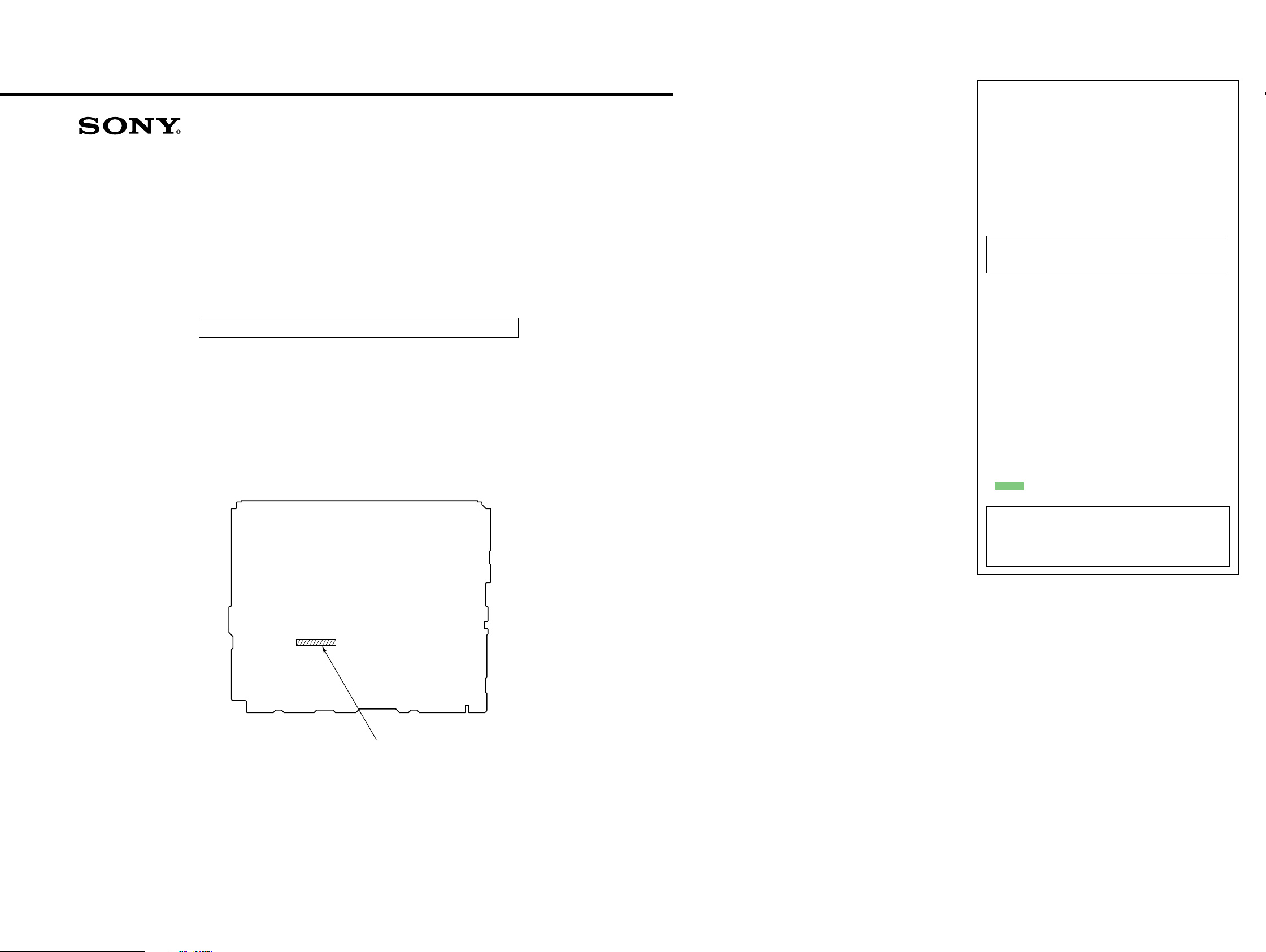
Subject : Change of Main Board
When performing service and inspection, check the part number of the main
boards.
(SPM-01001)
US Model
CDX-C4750
E Model
CDX-C6600
CDX-C4750/C6600
THIS NOTE IS COMMON FOR PRINTED WIRING
BOARDS AND SCHEMATIC DIAGRAMS.
(In addition to this, the necessary note is
printed in each block.)
for schematic diagram:
• All capacitors are in µF unless otherwise noted. pF: µµF
50 WV or less are not indicated except for electrolytics
and tantalums.
• All resistors are in Ω and 1/
specified.
• % : indicates tolerance.
f
•
• C : panel designation.
Note: The components identified by mark 0 or dotted line
• U : B+ Line.
• Power voltage is dc 14.4V and fed with regulated dc power
• Voltages are taken with a VOM (Input impedance 10 MΩ).
• Waveforms are taken with a oscilloscope.
• Circled numbers refer to waveforms.
• Signal path.
: internal component.
with mark 0 are critical for safety.
Replace only with part number specified.
supply from ACC and BATT cords.
Voltage variations may be noted due to normal produc-
tion tolerances.
Voltage variations may be noted due to normal produc-
tion tolerances.
F : FM
f : AM
J : CD
4
W or less unless otherwise
1. DISCRIMINATION
– MAIN BOARD (SIDE A) –
MAIN Board Part No.
Former : 1-672-438-11
New : 1-672-438-13
for printed wiring boards:
• X : parts extracted from the component side.
• Y : parts extracted from the conductor side.
a
•
• : Pattern from the side which enables seeing.
Caution:
Pattern face side: Parts on the pattern face side seen from the
(Side B) pattern face are indicated.
Parts face side: Parts on the parts face side seen from the
(Side A) parts face are indicated.
: Through hole.
(The other layer’s patterns are not indicated.)
9-926-441-82
2001B0400-1
© 2001. 2
Sony Corporation
Audio Entertainment Group
General Engineering Dept.
11

CDX-C4750/C6600
• Semiconductor Location
Ref. No. Location
(D402) C-3
D403 B-3
(D601) F-5
(D602) F-4
(D702) F-12
(D801) B-14
(D807) B-13
(D809) B-13
(D810) B-13
(D823) A-14
(D824) A-14
(D852) K-10
(D854) J-12
(D856) J-12
(D901) D-12
(D902) D-12
(D903) D-12
(D904) E-13
D909 D-9
D910 D-10
(D912) H-13
(D913) H-12
(D915) G-13
(D916) I-13
D918 J-9
D919 K-9
(D921) H-5
(D924) E-13
D930 C-9
(IC200) A-7
IC401 F-7
IC601 F-3
(IC702) F-11
IC801 J-7
IC803 D-14
(IC901) F-13
( ): SIDE B
1-1. PRINTED WIRING BOARD — MAIN SECTION —
Ref. No. Location
(IC902) I-6
Q110 B-4
Q111 B-4
Q210 C-4
Q211 C-5
(Q401) B-3
(Q402) C-3
(Q603) G-5
(Q609) G-5
(Q610) F-5
(Q612) F-5
(Q613) F-4
(Q614) G-3
Q615 F-5
(Q901) I-13
(Q902) I-13
(Q903) I-13
(Q904) G-13
Q905 C-9
Q906 D-11
Q907 I-12
Q908 I-12
(Q909) I-12
(Q910) H-13
(Q911) H-12
(Q912) H-13
Q913 G-13
Q914 K-9
Q915 K-9
Q916 D-9
Q917 C-10
Q918 C-10
Q919 G-13
Q921 H-5
Q924 D-12
Q925 D-11
22

CDX-C4750/C6600
33
 Loading...