

Sony AN-1016 Service Manual

Application Note AN-1016
Hermetic Surface-Mount Discrete Semiconductor,
Solutions to Assembly Integration
By
Tiva Bussarakons
Table of Contents
Page
Introduction ................................................................................................................. …….2
New Surface Mount Package Construction................................................................ …….3
TO-25x Package Construction....................................................................................…….4
D2 and D3 Packages.................................................................................................. …….4
Low Ohmic TO-257, TO-254, D2 and D3 ...................................................................…….5
Benefits of SMD over Leaded Packages.................................................................... …….6
Size and Weight Benefits....................................................................................…….6
Electrical Performance Benefits.......................................................................... …….7
SMD Assembly Integration Design Guidelines........................................................... …….9
Verification Methods for Attachment Integrity............................................................. …….12
SMD Rework Procedure .............................................................................................…….12
Conclusions................................................................................................................. …….12
This application note discusses the reliability and ruggedness issues of the ceramic leadless chip
carrier (CLCC), SMD and TO-25x hermetically sealed packages for high reliability design
applications.
www.irf.com
AN-1016
1
Introduction
A hermetically sealed package is generally required to house a semiconductor device to insure the
device’s reliability and ruggedness for high reliability design applications. Typical semiconductor devices
are MOSFETs (metal-oxide-semiconductor-field-effect-transistors), bipolar transistors, Schottky rectifiers,
PN junction diodes, and insulated gate bipolar transistors (IGBT). Hermetic surface mount packages,
leadless chip carriers (also known as LCC or CLCC) have served this function well and have been in
existence for more than 20 years. While the leaded packages (TO-257, TO-254, etc.) continue to find
their use in many current designs, a vast majority of new electronic equipment designs have been
integrating new surface mount packages, taking advantage of its smaller size, lighter weight, and the
excellent thermal performance that the new surface mount packages (SMD) offer. Many high frequency
circuit designs benefit from the inherently low inductance and low resistance these packages provide. In
many instances, the new SMDs are the absolute requirement. Figure 1 shows the hermetically sealed
packages that are discussed in the article, the ceramic leadless chip carrier (CLCC), the new SMD and the
leaded TO-25X packages.
Successful assembly integrations of plastic SMD devices are well established because of the temperature
coefficient of expansion (TCE) of the package is comparable to the industry’s standard board materials,
FR-4 and polyimide to which the devices are mounted. Additionally, the temperature range, coldest to
hottest temperature extremes where most assemblies with plastic SMD’s are required to operate, are
generally benign.
Unlike the plastic SMD, the popularity of the hermetic SMD devices has been somewhat hindered by the
TCE incompatibility of the SMD package and the board materials, and significantly wider operating
temperature demands. A soldered joint of a device to a PC board assembly can crack when it is subjected
to temperature extremes, i.e., during a soldering operation, environmental stress screening (ESS) or
temperature cycling screens. The ESS and temperature cycling screens simulate the assembly’s operating
environments prior to flight missions.
Solutions to the hermetic SMD assembly integration will be presented in this article. With the availability
of low TCE (temperature coefficient of expansion) board materials, advances in materials, innovative SMD
carrier designs, and maturity of the power module assembly technology, the hermetic SMD devices can
be now successfully and economically integrated in most of system designs. This article will focus on the
new generation hermetic surface mount packages hereafter referred to as ‘SMD’.
CLCC SMD TO-25X
Figure 1. Hermetically Sealed Packages (drawing is not to scale)
www.irf.com
AN-1016
2
Small
JC improvement of about 60%,
JC and
Bond Wire
Seal Ring
Housing
New Surface-Mount Package Construction
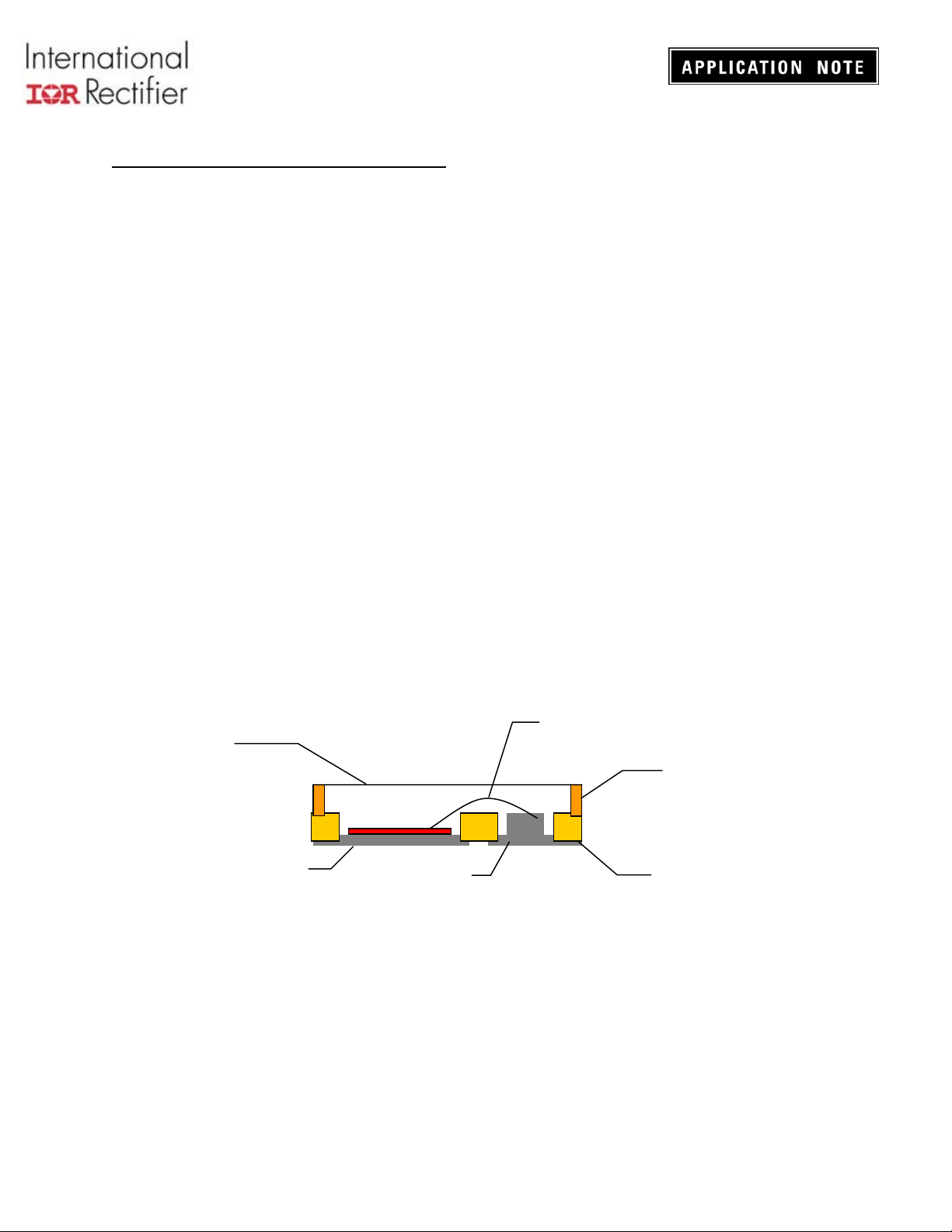
The new hermetic SMD package consists of three terminal pads, a ceramic housing, a seal ring, and a lid.
Figure 2 depicts the package structure. To insure the package’s integrity, the package materials are
carefully chosen to closely match the TCE of the silicon die, which has a TCE of 4.2 ppm/°C. Table 1 lists
TCE property of these materials. To minimize weight while achieving package’s ruggedness, the SMD
package uses relatively low mass density material in ceramic alumina (Al2O3) for housing. Higher mass
density alloys are used as needed to insure mechanical ruggedness, Kovar for lid and seal ring, and
copper-tungsten (CuW) for terminal pads. Additionally, package piece parts are shaped to eliminate
excess material without compromising the mechanical integrity. These piece parts are brazed together to
form a hermetic, semiconductor die housing. This results in smallest and lightest possible packages.
As illustrated in Figure 2, two smaller pads are gate and source terminals of a MOSFET device or anode
terminal(s) for a rectifier. A semiconductor die is soldered to the large terminal pad. This is typically a
drain terminal for a MOSFET device or a cathode terminal for a rectifier. It also serves as a thermal path
to an external heat sink. The thin structure of the pad provides a very short thermal path from the heat
source (die) to an external heat sink. Combined with the outstanding thermal conductivity property of
CuW, the package produces a very low thermal resistance path, thus a very low package junction-to-case
thermal resistance (θ
The SMD’s are a three-terminal device. The CLCC packages do offer up to 40 terminals in larger sizes and
as low as 3 terminals in a very small package. SMD package differs notably from its predecessor, the
CLCC surface mount package. One major difference is in the package base design where the CLCC uses
tungsten feed-through or metalized solid alumina (Al2O3), and as stated previously the SMD uses a thin
slice of CuW to minimize the package thermal resistance. This results in θ
1.67 °C/W for SMD .5 and about 4.5 °C/W for an equivalent CLCC with a same die size. With low θ
larger pad sizes, SMD’s find most of their use in higher current and higher power applications.
Conversely, the use of CLCC packages is limited to low current and low power applications.
Figure 2. SMD Package, Cross-Sectional View (drawing is not to scale)
Lid
JC).
Large
Terminal
Pad
Die
Terminal
pads (2X)
www.irf.com
AN-1016
3
Device
Elements
Die Silicon 4.2
Terminal
Pads
Housing Al2O3 6.4
Seal Ring Kovar 5.1
Lid Kovar 5.1
Table 1. TCE Property of Package Elements
TO-25X Package Construction
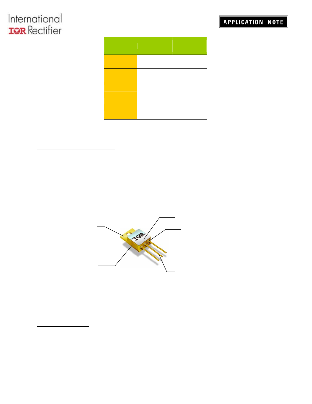
Figure 3 illustrates the construction of the leaded style TO-25X packages. The package uses relatively
high mass density materials such Kovar for the lid and seal ring, copper for frame, metalized BeO for
substrate (not shown), alloy 52 for leads, and copper-tungsten for base. The packages are sized to
facilitate die assembly and to accommodate internal leads extension. Moreover, external space is required
for leads extension. All these factors result in a larger and heavier package than a comparable SMD
package. While the base of a TO-25X package is more than 3 times the thickness of the SMD’s, .050” vs.
.015”, their thermal resistances are however, comparable.
Note: Substrate is attached to the base internally and it is not shown.
Figure 3. TO-25X Package Construction
CuW
Base
Copper
Frame
Material
CuW 6
TCE
(ppm/°C)
Kovar Lid
Al2O3 Ceramic
Eyelet (3)
Alloy 52 Leads (3)
D2 and D3 Packages
D2 and D3 packages are basically tab-less TO-257 and tab-less TO-254, respectively. They are now
available as standard package options. These packages use similar package materials and have the same
basic construction as the TO-257 and TO-254, but have smaller footprints than their counterparts. The
other difference is the leads configuration where leads of D2 and D3 packages are formed for surfacemount assembly. Refer to Figure 4 for these packages. Weight, thermal resistance and foot print data of
various SMD’s and leaded styles including the new D2 and D3 packages are shown in Table 2.
www.irf.com
AN-1016
4
 Loading...