


21FL94
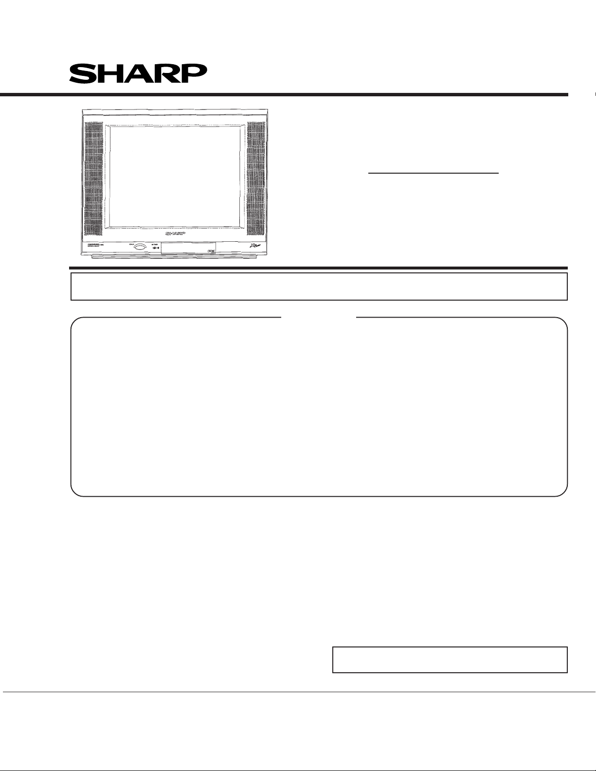
21FL94
SHARP CORPORATION
This document has been published to be used for after
sales service only.
The contents are subject to change without notice.
In the interests of user-safety (Required by saf ety regulations in some countries ) the set should be restored to its
original condition and only parts identical to those specified should be used.
COLOR TELEVISION
Chassis No. GA-4
Page
» ELECTRICAL SPECIFICATIONS .........................................................................................................1
» IMPORTANT SERVICE SAFETY PRECAUTION .................................................................................2
» LOCATION OF USER'S CONTROL .....................................................................................................4
» INSTALLATION AND SERVICE INSTRUCTIONS................................................................................5
» SERVICE MODE ..................................................................................................................................6
» ADJUSTMENT METHOD ...................................................................................................................12
» WAVEFORMS .....................................................................................................................................25
» CHASSIS LAYOUT .............................................................................................................................26
» BLOCK DIAGRAM ..............................................................................................................................27
» DESCRIPTION OF SCHEMATIC DIAGRAM......................................................................................31
» SCHEMATIC DIAGRAMS ...................................................................................................................32
» PRINTED WIRING BOARD ASSEMBLIES ........................................................................................36
» REPLACEMENT PARTS LIST............................................................................................................40
» PACKING OF THE SET ......................................................................................................................46
CONTENTS
SPEAKER
SIZE ...................................................................12 x 5 cm, 2pcs
VOICE COIL IMPEDANCE............................. 16 ohm at 400 Hz
ANTENNA INPUT IMPEDANCE
VHF/UHF.....................................................75 ohm Unbalanced
TUNING RANGES
VHF-Channels...............................................................2 thru 13
UHF-Channels ............................................................14 thru 69
CATV Channels ...........................................................1 thru 125
(EIA, Channel Plan U.S.A.)
POWER INPUT....................................... AC 110~220 V, 50/60 Hz
POWER RATING .................................................................... 90W
PICTURE SIZE .......................................... 1,239 cm
2
(192sq inch)
CONVERGENCE ............................................................. Magnetic
SWEEP DEFLECTION .................................................... Magnetic
FOCUS .................................................. QFP/UNI-B1 Electrostatic
INTERMEDIATE FREQUENCIES
Picture IF Carrier Frequency ..................................... 45.75 MHz
Sound IF Carrier Frequency...................................... 41.25 MHz
Color Sub-Carrier Frequency .................................... 42.17 MHz
(Nominal)
AUDIO POWER
OUTPUT RATING ........................................4.0 W(RMS) x 2pcs
Specifications are subject to change without
prior notice.
ELECTRICAL SPECIFICATIONS
MODEL
SERVICE MANUAL
21FL94
S64T921FL94//

2
21FL94
IMPORTANT SERVICE SAFETY PRECAUTION
Ë
Service work should be performed only by qualified service technicians who are
thoroughly familiar with all safety checks and the servicing guidelines which follow:
X-RADIATION AND HIGH VOLTAGE LIMITS
1. Be sure all service personnel are aware of the
procedures and instructions covering X-radiation.
The only potential source of X-ray in current solid
state TV receivers is the picture tube. However, the
picture tube does not emit measurable X-Ray
radiation, if the high voltage is as specified in the
"High Voltage Check" instructions.
It is only when high voltage is excessive that X-
radiation is capable of penetrating the shell of the
picture tube including the lead in the glass material.
The important precaution is to keep the high voltage
below the maximum level specified.
2. It is essential that servicemen have available at all
times an accurate high voltage meter.
The calibration of this meter should be checked
periodically.
3. High voltage should always be kept at the rated value
−no higher. Operation at higher voltages may cause
a failure of the picture tube or high voltage circuitry
and;also, under certain conditions, may produce
radiation in exceeding of desirable levels.
4. When the high voltage regulator is operating properly
there is no possibility of an X-radiation problem.
Every time a color chassis is serviced, the brightness
should be tested while monitoring the high voltage
with a meter to be certain that the high voltage does
not exceed the specified value and that it is regulating
correctly .
5. Do not use a picture tube other than that specified
or make unrecommended circuit modifications to the
high voltage circuitry.
6. When trouble shooting and taking test
measurements on a receiver with excessive high
voltage, avoid being unnecessarily close to the
receiver.
Do not operate the receiver longer than is necessary
to locate the cause of excessive voltage.
WARNING
1. For continued safety, no modification of any circuit
should be attempted.
2. Disconnect AC power before servicing.
3. Semiconductor heat sinks are potential shock
hazards when the chassis is operating.
4. The chassis in this receiver has two ground systems
which are separated by insulating material. The non-
isolated (hot) ground system is for the B+ voltage
regulator circuit and the horizontal output circuit. The
isolated ground system is for the low B+ DC voltages
and the secondary circuit of the high voltage
transformer.
To prevent electrical shock use an isolation
transformer between the line cord and power
receptacle, when servicing this chassis.
SERVICING OF HIGH VOLTAGE SYSTEM
AND PICTURE TUBE
When servicing the high voltage system,
remove the static charge by connecting a
10k ohm resistor in series with an insulated
wire (such as a test probe) between the pic-
ture tube ground and the anode lead. (AC
line cord should be disconnected from AC
outlet.)
1. Picture tube in this receiver employs integral
implosion protection.
2. Replace with tube of the same type number for
continued safety.
3. Do not lift picture tube by the neck.
4. Handle the picture tube only when wearing
shatterproof goggles and after discharging the high
voltage anode completely.
3
21FL94
2345678901234567890123456789012123456789012345678901234567890121234567890123456789012345678901212
3
2345678901234567890123456789012123456789012345678901234567890121234567890123456789012345678901212
3
SAFETY NOTICE
Many electrical and mechanical parts in television
receivers have special safety-related characteristics.
These characteristics are often not evident from visual
inspection, nor can protection afforded by them be
necessarily increased by using replacement components
rated for higher voltage, wattage, etc.
Replacement parts which have these special safety
characteristics are identified in this manual; electrical
components having such features are identified by "å"
and shaded areas in the Replacement Parts Lists and
Schematic Diagrams.
IMPORTANT SERVICE SAFETY PRECAUTION
(Continued)
1. Inspect all lead dress to make certain that leads are
not pinched or that hardware is not lodged between
the chassis and other metal parts in the receiver.
2. Inspect all protective devices such as non-metallic
control knobs, insulating materials, cabinet backs,
adjustment and compartment covers or shields,
isolation resistor-capacity networks, mechanical
insulators, etc.
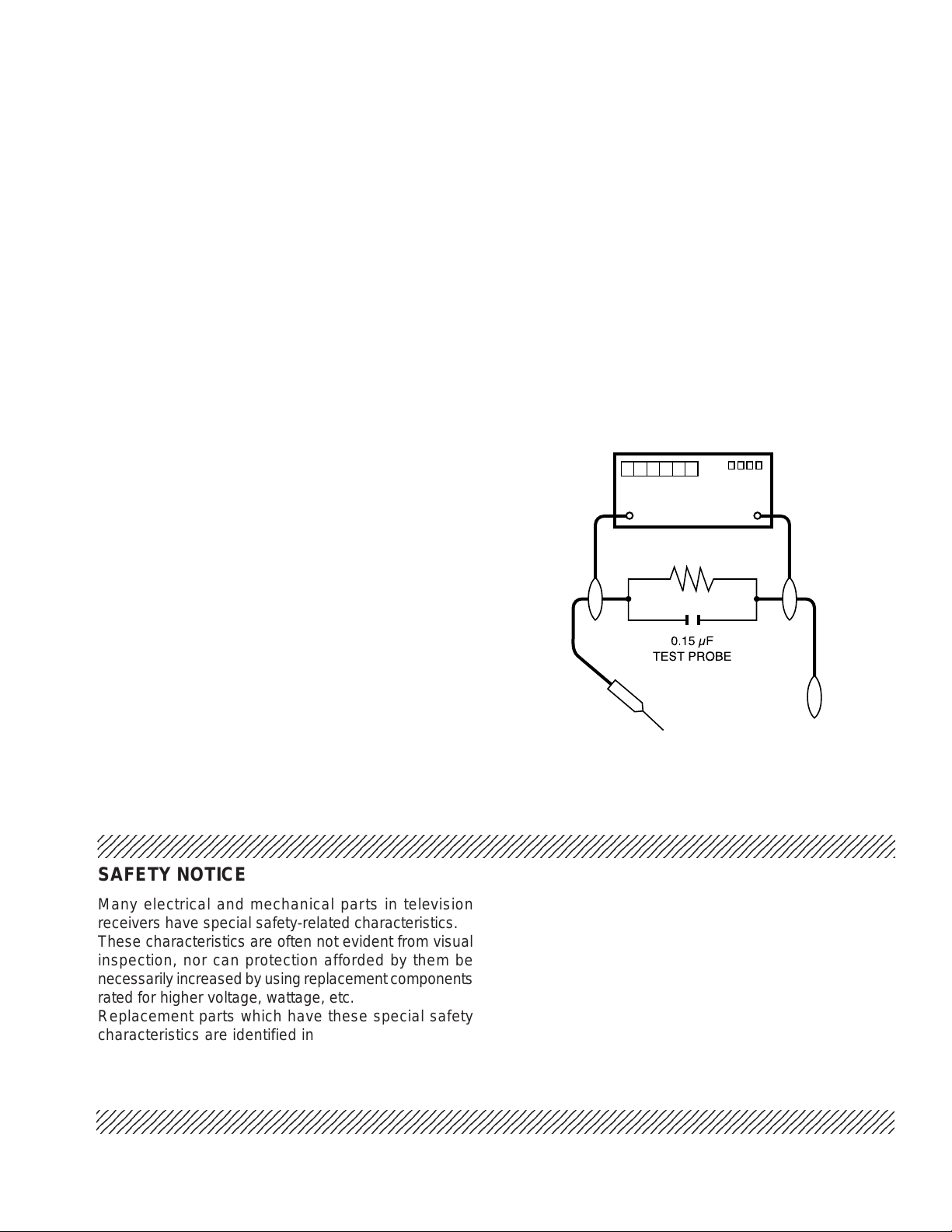
3. To be sure that no shock hazard exists, check for
leakage current in the following manner.
• Plug the AC cord directly into a 110~220 volt AC
outlet, (Do not use an isolation transformer for this
test).
• Using two clip leads, connect a 1.5k ohm, 10 watt
resistor paralleled by a 0.15µF capacitor in series
with all exposed metal cabinet parts and a known
earth ground, such as electrical conduit or electrical
ground connected to earth ground.
• Use an AC voltmeter ha ving with 5000 ohm per volt,
or higher, sensitivity to measure the A C v oltage drop
across the resistor.
BEFORE RETURNING THE RECEIVER
(Fire & Shock Hazard)
Before returning the receiver to the user, perform
the following safety checks.
• Connect the resistor connection to all exposed metal
parts having a return to the chassis (antenna, metal
cabinet, screw heads, knobs and control shafts,
escutcheon, etc.) and measure the AC voltage drop
across the resistor.
AII checks must be repeated with the AC line cord
plug connection reversed. (If necessary, a non-
polarized adapter plug must be used only for the
purpose of completing these check.)
Any current measured must not exceed 0.5 milliamp.
Any measurements not within the limits outlined
above indicate of a potential shock hazard and
corrective action must be taken before returning the
instrument to the customer.
For continued protection, replacement parts must be
identical to those used in the original circuit. The use of
substitute replacement parts which do not have the same
safety characteristics as the factory recommended
replacement parts shown in this service manual, may
create shock, fire, X-radiation or other hazards.
DVM
AC SCALE
1.5k ohm
10W
TO EXPOSED
METAL PARTS
CONNECT TO
KNOWN EARTH
GROUND
234567890123456789012345678901212345678901234567890123456789012123456789012345678901234567890121
2
234567890123456789012345678901212345678901234567890123456789012123456789012345678901234567890121
2
4
21FL94
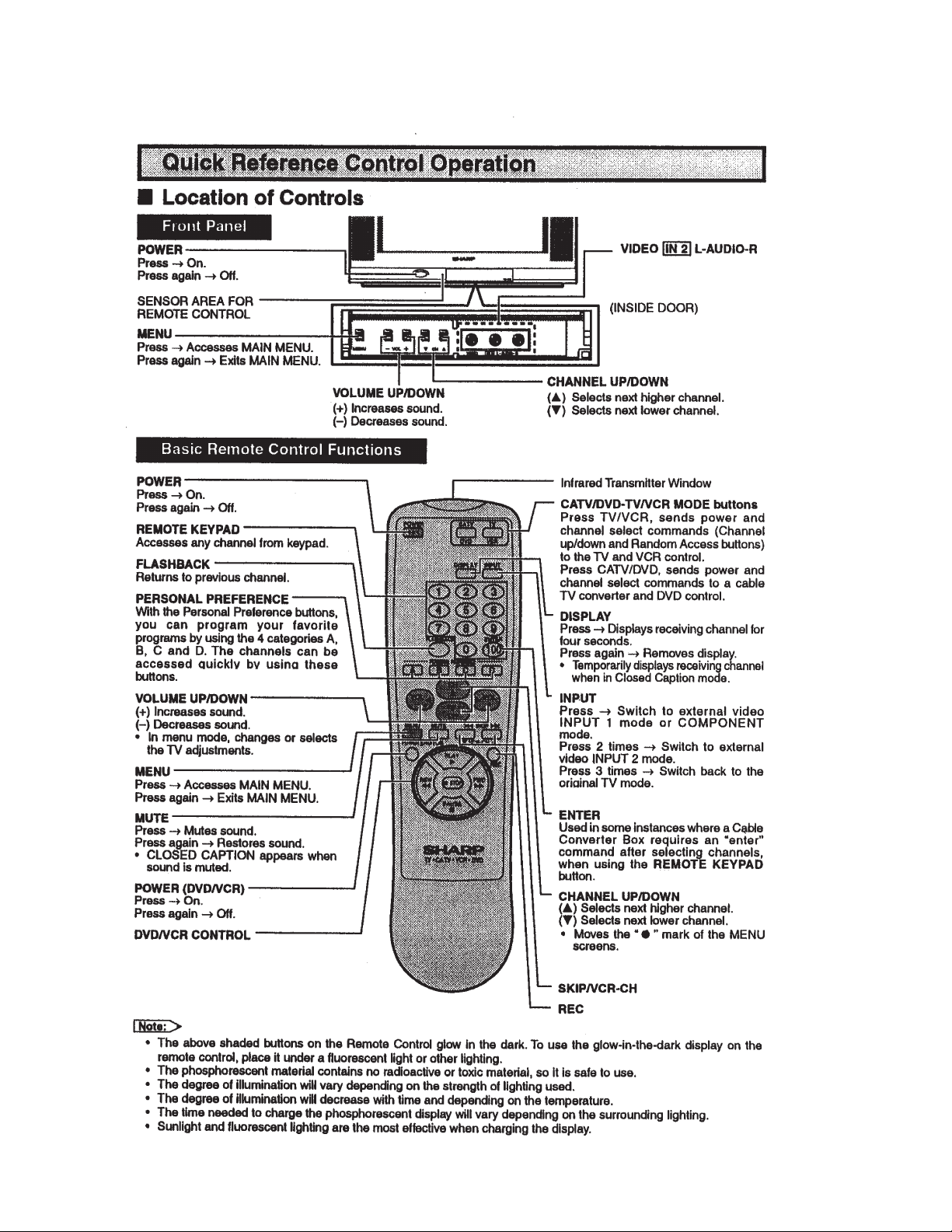
LOCATION OF USER'S CONTROL

5
21FL94
CIRCUIT PROTECTION
The receiver is protected by a 3.15A fuse (F701),
mounted on PWB-A, wired into one side of the AC
line input.
X-RADIATION PROTECTOR CIRCUIT TEST
After service has been performed on the horizontal
deflection system, high voltage system, B+ system,
test the X-Radiation protection circuit to ascertain
proper operation as follows:
1. Apply 110~220V AC using a variac transformer for
accurate input voltage.
2. Allow for warm up and adjust all customer controls
for normal picture and sound.
3. Receive a good local channel.
4. Connect a digital voltmeter to P603 pin3 and make
sure that the voltmeter reads 20 ±1.1V.
5. Apply external 27V DC at P603 pin3 by using an
external DC supply, TV must be shut off.
6. To reset the protector, unplug the AC cord and mak e
a short circuit between P603 pin1 and P603 pin2.
Now make sure that normal picture appears on the
screen.
7. If the operation of the horizontal oscillator does not
stop in step 5, the circuit must be repaired before the
set is returned to the customer.
HIGH VOLTAGE CHECK
High voltage is not adjustable but must be checked
to verify that the receiver is operating within safe
and efficient design limitations as specified checks
should be as follows:
1. Connect an accurate high voltage meter between
ground and anode of picture tube.
2. Operate receiver for at least 15 minutes at 110~220V
AC line voltage, with a strong air signal or a properly
tuned in test signal.
3. Enter the service mode and set Y-mute ON by using
Service R/C.
4. The voltage should be approximately 28.7kV (at zero
beam).
If a correct reading cannot be obtained, check circuitry
for malfunctioning components. After the v oltage test,
make Y-mute off to the normal mode.
INSTALLATION AND SERVICE INSTRUCTIONS
Note: (1)When performing any adjustments to resistor controls and transformers use non-metallic
screwdrivers or TV alignment tools.
(2)Before performing adjustments, the TV set must be on at least 15 minutes.
6
21FL94
Service Mode Overview
1. Service mode is entered by SERVICE key input or CH-UP +VOL-DOWN input during reset.
2. Service mode is cleared by entering SERVICE key command during service mode.
3. If key input port (SERVICE) input is LOW, then it is in service mode.
4. During key input port (SERVICE) input is LOW, clearing service mode by key input SERVICE is disabled.
5. Service mode can be switched to 4 modes as follows by key input MENU;
SERVICE MODE
6. AFT processing is disabled during service mode. PLL setting data is set to fo data.
7. All user data are set to default during service mode. FAO and SPEAKER user settings are off and on respectively
in service mode. Energy Save is off.
8. Sleep timer, View timer, on timer and off timer are inactivated in Service mode.
9. Sound is muting in service mode except at Adjustment Items V20, M01, M03, M04, M05, and M06.
Adjustment mode
Setting mode
First mode of service mode when SERVICE key is
pressed.
First mode of service mode when local key
CH-UP + VOL-DOWN is pressed after MCU reset.
Option mode
Check mode
7
21FL94
Adjustment Mode Items
No. Item Name IC Register Range Default
V01 SUB-PICTURE 1 Chip CONTRAST 0~127 127
V02 SUB-TINT 1 Chip TINT 0~127 64
V03 SUB-COLOR 1 Chip COLOR 0~127 64
V04 SUB-BRIGHT 1 Chip BRIGHT 0~255 128
V05 SUB-SHARP 1 Chip VIDEO-TONE 0~63 32
V06 V-SHIFT 1 Chip V-SHIFT 0~7 4
V07 H-SHIFT 1 Chip H-PHASE 0~31 16
V08 RF-AGC 1 Chip RF-DELAY 0~127 127
V09 V-SIZE 1 Chip V-SIZE 0~63 32
V10 PIF-VCO 1 Chip VIF-VCO 0~63 32
V11 R-CUTOFF 1 Chip R-CUTOFF 0~255 127
V12 G-CUTOFF 1 Chip G-CUTOFF 0~255 127
V13 B-CUTOFF 1 Chip B-CUTOFF 0~255 127
V14 R-DRIVE 1 Chip R-DRIVE 0~127 64
V15 B-DRIVE 1 Chip B-DRIVE 0~127 64
V16 SUB-COLOR(YUV) 1 Chip COLOR 0~127 64
V17 SUB-TINT(YUV) 1 Chip BASEBAND-TINT 0~127 64
V18 CC-POS MICON CC-POS 0~255 32
V19 SCREEN CUT OFF 1 Chip CUT OFF 0~2 0
V20 SUB-VOL 1 Chip A-ATT 0~127 127
V21 H-VCO 1 Chip H-VCO 0~7 4
M01 MTS-ATT MTS ATT (MTS) 0~15 10
M02 MTS-VCO MTS VCO (MTS) 0~63 32
M03 MTS-FILTER MTS FILTER (MTS) 0~63 28
M04 MTS-WIDEBAND MTS WIDEBAND (MTS) 0~63 27
M05 MTS-SPECTRAL MTS SPECTRAL (MTS) 0~63 32
M06 SUB-VOL MTS VOL (MTS) 0~63 63

8
21FL94
Ë
SELF ADJUSTMENT
H-VCO
1. When there is H-VCO self-adjustment key input for adjustment item H-VCO, self-adjustment is performed.
2. H-FREE(1chip) is set to 1.
3. H-OUT is set by intelligent monitor output.
4. IM input is set as TIM input.
5. H-VCO(1chip) data is changed so that the number of input pulse is 125 inside 8ms interval.
6. When adjustment completed, OSD display and H-VCO self-adjustment status data of EEPROM are updated.
7. H-FREE(1chip), intelligent monitor output and IM input mode are recovered.
RF-AGC
1. When there is RF-AGC self-adjustment key input for adjustment item RF-AGC, self-adjustment is performed.
2. AGC-OUT is set by intelligent monitor output.
3. IM input is set as AD input.
4. By decreasing RF-AGC (1chip) data from current RF-AGC adjustment value to 0, AFT input voltage becomes the
maximum setting value.
5. Increase RF-AGC(1chip) data, when AFT input voltage is at (max. 0.3V) point, adjustment is completed.
6. When adjustment completed, OSD display and RF-AGC self-adjustment status data of EEPROM are updated.
7. Intelligent monitor output and IM input mode are recovered.
PIF-VCO
1. When there is PIF-VCO self-adjustment key input for adjustment item PIF-VCO, self-adjustment is performed.
2. VIF-DEF(1chip) is set to 1.
3. AFC is set by intelligent monitor output.
4. IM input is set as AD input.
5. VIF-VCO(1chip) data is changed so that input voltage becomes 2.5V.
6. When adjustment completed, OSD display and PIF-VCO self-adjustment status data of EEPROM are updated.
7. VIF-DEF(1chip), intelligent monitor output and IM input mode are recovered.
9
21FL94
Setting Mode Items
No. Item Name IC Register Range Default
F01 VIDEO TONE -GAIN (TV) 1 Chips V-TONE 0/1 0
F02 VIDEO TONE -GAIN (AV) 1 Chips V-TONE 0/1 0
F03
VIDEO TONE -GAIN (S-AV)
1 Chips V-TONE 0/1 0
F04 VIDEO TONE -GAIN(YUV) 1 Chips V -T ONE 0/1 0
F05 ABCL 1 Chips ABCL 0/1 0
F06 BS 1 Chips BS-OFF 0/1 0
F07 ABCL-G 1 Chips ABCL-G 0/1 0
F08 SHP-AV OFFSET VIDEO-TONE(OFFSET) -16~+16 0
F09 SHP-SAV OFFSET VIDEO-TONE(OFFSET) -16~+16 0
F10 SHP-YUV OFFSET VIDEO-TONE(OFFSET) -16~+16 0
F11 RGB-CLIP 1 Chips EXTRGB-CLIP 0/1 0
F12 E-SAVE OFFSET CONTRAST(OFFSET) 0~63 30
F13 FAO-VOL 1 Chips A-ATT 0~127 120
F14 PIF-G 1 Chips VIF-GAIN 0~7 4
F15 Y-DELAY(TV) 1 Chips Y-DELAY 0~7 0
F16 Y-DELAY(AV) 1 Chips Y-DELAY 0~7 0
F17 Y-DELAY(SAV) 1 Chips Y-DELAY 0~7 0
F18 Y-DELAY(YUV) 1 Chips Y-DELAY 0~7 0
F19 TINT-AV OFFSET TINT(OFFSET) -32~+32 0
F20 TINT-SAV OFFSET TINT(OFFSET) -32~+32 0
F21 COL-AV OFFSET COLOR(OFFSET) -32~+32 0
F22 COL-SAV OFFSET COLOR(OFFSET) -32~+32 0
F23 R-DRI(R2) OFFSET R-DRI(OFFSET) -32~+32 0
F24 R-DRI( R) OFFSET R-DRI(OFFSET) -32~+32 0
F25 R-DRI(B) OFFSET R-DRI(OFFSET) -32~+32 0
F26 B-DRI(R2) OFFSET B-DRI(OFFSET) -32~+32 0
F27 B-DRI( R) OFFSET B-DRI(OFFSET) -32~+32 0
F28 B-DRI(B) OFFSET B-DRI(OFFSET) -32~+32 0
F29 V-FREE 1 Chips V-FREE 0/1 0
F30 GAMMA 1 Chips GAMMA 0~3 0
F31 TRAP(TV) 1 Chips TRAP-FINE 0~3 2
F32 TRAP(AV) 1 Chips TRAP-FINE 0~3 2
F33 H-FREE 1 Chips H-FREE 0/1 0
F34 1W(TV) 1 Chips V.WINDOW 0/1 0
F35 1W(AV) 1 Chips V.WINDOW 0/1 0
F36 YLPF 1 Chips YSW-LPF 0/1 1
F37 BS-D 1 Chips BS-DISCHARGE 0~3 0
F38 BS-C 1 Chips BS-CHARGE 0~3 0
F39 SL(TV) 1 Chips S-SLICE DOWN 0~3 0
F40 SL(AV) 1 Chips S-SLICE DOWN 0~3 0
F41 SL(SAV) 1 Chips S-SLICE DOWN 0~3 0
F42 SL(YUV) 1 Chips S-SLICE DOWN 0~3 0
F43 AFC2 1 Chips AFC2-G 0/1 0
F44 VD(TV) 1 Chips VSYNC-DET 0/1 0
F45 VD(AV) 1 Chips VSYNC-DET 0/1 0
F46 AS(TV) 1 Chips AUTO-SLICE 0/1 0
F47 AS(AV) 1 Chips AUTO-SLICE 0/1 0
F48 AS(SAV) 1 Chips AUTO-SLICE 0/1 0
F49 AS(YUV) 1 Chips AUTO-SLICE 0/1 0
F50 FBP(TV) 1 Chips FBP VTH 0/1 0
F51 FBP(AV) 1 Chips FBP VTH 0/1 0
F52 FBP(SAV) 1 Chips FBP VTH 0/1 0
F53 FBP(YUV) 1 Chips FBP VTH 0/1 0
F54 C.CLIP LEVEL 1 Chips C.CLIP LEVEL 0/1 0
10
21FL94
Setting Mode Items (Continued)
No. Item Name IC Register Range Default
F55 PSW MTS PSW 0/1 0
F56 FAO-VOL MTS VOL 0~63 60
F57 CP PLL CHARGE PUMP 0/1 0
F58 CC LEVEL MICON CC LEVEL 0/1 0
F59 OSD POS MICON OSD POS 0/1 0
F60 OFFSET-ADJ-COL 1 Chips COLOR -32~+32 0
F61 OFFSET-ADJ-TINT 1 Chips TINT -32~+32 0
F62 OFFSET-ADJ-TINT-YUV 1 Chips BASEBAND-TINT -32~+32 0
F63 TIMER4-LOW SPEED 1 Chips TIMER4 VALUE 0~225 50
F64 TIMER4-HIGH SPEED 1 Chips TIMER4 VALUE 0~225 125
F65 R-CUT-YUV 1 Chips R-CUT(OFFSET) -63~+63 0
F66 G-CUT-YUV 1 Chips G-CUT(OFFSET) -63~+63 0
F67 B-CUT-YUV 1 Chips B-CUT(OFFSET) -63~+63 0
F68 R-DRI-YUV 1 Chips R-DRI(OFFSET) -63~+63 0
F69 B-DRI-YUV 1 Chips B-DRI(OFFSET) -63~+63 0
F70 CLOCK-ADJ 1 Chips 0~25 25
11
21FL94
Option Mode Items
No
OPTION FUNCTION
01
Default Data
001 DEMO Without DEMO With DEMO 1
002 DOWNLOAD Without V-CHIP OP With V-CHIP OP 0
003 V -CHIP Without V-CHIP With V-CHIP 0
004 SPEAKER Without SPEAKER With SPEAKER 1
005 FAO Without FAO With FAO 1
006 P.PREF Without P.REF With P.REF 1
007 UNIV+ Without UNIV+ With UNIV+ 1
008 VIEW TIMER Without VIEW TIMER With VIEW TIMER 1
009 EZ-SETUP EZ-SETUP A UTO PRESET 0
010 PON-CH Without POWER-ON With POWER-ON 0
011 FAV-COL FAV-COL COL-TEMP 1
012 COMPONENT Without COMPONENT With COMPONENT 1
013 AV Without AV With AV 1
014 AV2 AV1 system AV2 system 1
015 MTS Without MTS With MTS 1
016 TONE-CTRL Without S-ADJ With S-ADJ 1
017 AUTO-OFF Without AUTO-OFF With AUTO-OFF 1
018 INIT-LANG ENGLISH SPANISH 1
019 SETUP-FLAG NO SET UP AUTO SET UP 1
020 AV-FR
"0"=NO AV "1"=REAR "2"=FRONT "3"=REAR & FRONT
3
021 AV3/S-IN Without AV3/S-IN With AV3/S-IN 0
022 COMB Without COMB With COMB 0
023 AUTO-INPUT Without AUTO-INPUT With AUTO-INPUT 1
024 CLOCK Without CLOCK With CLOCK 1
025 LED SEMEX MODEL SPC MODEL 0
026 FLAT Not FLAT MODEL FLAT MODEL 1
027 BASS BOOST Without BASS BOOST With BASS BOOST 0
028 DSE Without DSE With DSE 0
029 SRS Without SRS With SRS 0
030 WHITE-OUT Without WHITE-OUT With WHITE-OUT 1
Check Mode
Micron mask version, software version and ROM correction function status are displayed in check mode.
12
21FL94
ADJUSTMENT METHOD
Caution:to get into the service mode, one of the ways is press direct key for service items. the other ways
is short the main chassis JA301 and JA410
There is three stage of Service Mode data
First stage data from V01 ~ M06
to go into second stage of service mode data, press MENU key
Second stage data from F01 ~ F70
to go into third stage of service mode data, press MENU key
Third stage data from 001 ~ 030
Below is the contents of these data
First Stage
Auto Adjustment Item
1. H-VCO
2. RF-AGC
3. PIF-VCO
Data Service Mode Function Range Default Data
V01 SUB-PICTURE CONTRAST 0~127 127
V02 SUB-TINT TINT 0~127 64
V03 SUB-COLOR COLOR 0~127 64
V04 SUB-BRIGHT BRIGHT 0~255 128
V05 SUB-SHARP VIDEO-TONE 0~63 32
V06 V-SHIFT V-SHIFT 0~7 4
V07 H-SHIFT H-PHASE 0~31 16
V08 RF-AGC RF-DELAY 0~127 127
V09 V-SIZE V-SIZE 0~63 32
V10 PIF-VCO VIF-VCO 0~63 32
V11 R-CUTOFF R-CUTOFF 0~255 127
V12 G-CUTOFF G-CUTOFF 0~255 127
V13 B-CUTOFF B-CUTOFF 0~255 127
V14 R-DRIVE R-DRIVE 0~127 64
V15 B-DRIVE B-DRIVE 0~127 64
V16 SUB-COLOR(YUV) COLOR 0~127 64
V17 SUB-TINT(YUV) BASEBAND-TINT 0~127 64
V18 CC-POS CC-POS 0~255 32
V19 SCREEN CUT OFF CUT OFF 0~2 0
V20 SUB-VOL A-ATT 0~127 127
V21 H-VCO H-VCO 0~7 4
M01 MTS-ATT ATT (MTS) 0~15 10
M02 MTS-VCO VCO (MTS) 0~63 32
M03 MTS-FILTER FILTER (MTS) 0~63 28
M04 MTS-WIDEBAND WIDEBAND (MTS) 0~63 27
M05 MTS-SPECTRAL SPECTRAL (MTS) 0~63 32
M06 SUB-VOL VOL (MTS) 0~63 63
13
21FL94
Data Service Mode Function Range Default Data
F01 VIDEO TONE -GAIN (TV) V-TONE 0/1 0
F02 VIDEO TONE -GAIN (AV) V-TONE 0/1 0
F03 VIDEO TONE -GAIN (S-AV) V-TONE 0/1 0
F04 VIDEO TONE -GAIN(YUV) V -T ONE 0/1 0
F05 ABCL ABCL 0/1 0
F06 BS BS-OFF 0/1 0
F07 ABCL-G ABCL-G 0/1 0
F08 SHP-AV VIDEO-TONE(OFFSET) -16~+16 0
F09 SHP-SAV VIDEO-T ONE(OFFSET) -16~+16 0
F10 SHP-YUV VIDEO-TONE(OFFSET) -16~+16 0
F11 RGB-CLIP EXTRGB-CLIP 0/1 0
F12 E-SAVE CONTRAST(OFFSET) 0~63 30
F13 FAO-V OL A-A TT 0~127 120
F14 PIF-G VIF-GAIN 0~7 4
F15 Y -DELAY(TV) Y -DELAY 0~7 0
F16 Y -DELAY(AV) Y-DELA Y 0~7 0
F17 Y -DELAY(SAV) Y-DELA Y 0~7 0
F18 Y -DELAY(YUV) Y-DELAY 0~7 0
F19 TINT -A V TINT(OFFSET) -32~+32 0
F20 TINT -SA V TINT(OFFSET) -32~+32 0
F21 COL-AV COLOR(OFFSET) -32~+32 0
F22 COL-SAV COLOR(OFFSET) -32~+32 0
F23 R-DRI(R2) R-DRI(OFFSET) -32~+32 0
F24 R-DRI( R) R-DRI(OFFSET) -32~+32 0
F25 R-DRI(B) R-DRI(OFFSET) -32~+32 0
F26 B-DRI(R2) B-DRI(OFFSET) -32~+32 0
F27 B-DRI( R) B-DRI(OFFSET) -32~+32 0
F28 B-DRI(B) B-DRI(OFFSET) -32~+32 0
F29 V-FREE V-FREE 0/1 0
F30 GAMMA GAMMA 0~3 0
F31 TRAP(TV) TRAP-FINE 0~3 2
F32 TRAP(AV) TRAP-FINE 0~3 2
F33 H-FREE H-FREE 0/1 0
F34 1W(TV) V.WINDOW 0/1 0
F35 1W(AV) V.WINDOW 0/1 0
F36 YLPF YSW-LPF 0/1 1
F37 BS-D BS-DISCHARGE 0~3 0
F38 BS-C BS-CHARGE 0~3 0
F39 SL(TV) S-SLICE DOWN 0~3 0
F40 SL(AV) S-SLICE DOWN 0~3 0
F41 SL(SAV) S-SLICE DOWN 0~3 0
F42 SL(YUV) S-SLICE DOWN 0~3 0
F43 AFC2 AFC2-G 0/1 0
F44 VD(TV) VSYNC-DET 0/1 0
F45 VD(AV) VSYNC-DET 0/1 0
F46 AS(TV) AUTO-SLICE 0/1 0
F47 AS(AV) AUTO-SLICE 0/1 0
F48 AS(SAV) AUTO-SLICE 0/1 0
F49 AS(YUV) AUTO-SLICE 0/1 0
F50 FBP(TV) FBP VTH 0/1 0
F51 FBP(AV) FBP VTH 0/1 0
F52 FBP(SAV) FBP VTH 0/1 0
F53 FBP(YUV) FBP VTH 0/1 0
F54 C.CLIP LEVEL C.CLIP LEVEL 0/1 0
F55 PSW PSW 0/1 0
F56 FAO-VOL VOL 0~63 60
Second Stage
14
21FL94
Data Service Mode Function Range Default Data
F57 CP CHARGE PUMP 0/1 0
F58 CC LEVEL CC LEVEL 0/1 0
F59 OSD POS OSD POS 0/1 0
F60 OFFSET-ADJ-COL COLOR -32~+32 0
F61 OFFSET-ADJ-TINT TINT -32~+32 0
F62 OFFSET-ADJ-TINT-YUV BASEBAND-TINT -32~+32 0
F63 TIMER4-LOW SPEED TIMER4 VALUE 0~225 50
F64 TIMER4-HIGH SPEED TIMER4 VALUE 0~225 125
F65 R-CUT-YUV R-CUT(OFFSET) -63~+63 0
F66 G-CUT-YUV G-CUT(OFFSET) -63~+63 0
F67 B-CUT-YUV B-CUT(OFFSET) -63~+63 0
F68 R-DRI-YUV R-DRI(OFFSET) -63~+63 0
F69 B-DRI-YUV B-DRI(OFFSET) -63~+63 0
F70 CLOCK-ADJ 0~25 25
Second Stage (Continued)
Third Stage
*
*POWER ON BY CH-UP/CH-DOWN KEY
Data OPTION FUNCTION DATA = "0" DATA ="1" Default Data
001 DEMO DEMO DISABLE ENABLE 1
002 DOWNLOAD V-CHIP OP DISABLE ENABLE 0
003 V-CHIP V-CHIP DISABLE ENABLE 0
004 SPEAKER SPEAKER DISABLE ENABLE 1
005 FAO FAO DISABLE ENABLE 1
006 P.PREF P.REF DISABLE ENABLE 1
007 UNIV+ UNIV+ DISABLE ENABLE 1
008 VIEW TIMER VIEW TIMER DISABLE ENABLE 1
009 EZ-SETUP EZ-SETUP AUTO PRESET 0
010 * PON-CH POWER-ON DISABLE ENABLE 0
011 FAV-COL FAV-COL COL-TEMP 1
012 COMPONENT COMPONENT DISABLE ENABLE 1
013 AV AV DISABLE ENABLE 1
014 AV2 AV1 AV2 1
015 MTS MTS DISABLE ENABLE 1
016 TONE-CTRL S-ADJ DISABLE ENABLE 1
017 AUTO-OFF AUTO-OFF DISABLE ENABLE 1
018 INIT-LANG ENGLISH SPANISH 1
019 SETUP-FLAG NO SET UP AUTO SET UP 1
020 AV-FR
"0"=NO AV "1"=REAR "2"=FRONT "3"=REAR & FRONT
3
021 AV3/S-IN AV3/S-IN DISABLE ENABLE 0
022 COMB COMB DISABLE ENABLE 0
023 AUTO-INPUT AUTO-INPUT DISABLE ENABLE 1
024 CLOCK CLOCK DISABLE ENABLE 1
025 LED SEMEX MODEL SPC MODEL 0
026 FLAT FLAT DISABLE ENABLE 1
027 BASS BOOST BASS BOOST DISABLE ENABLE 0
028 DSE DSE DISABLE ENABLE 0
029 SRS SRS DISABLE ENABLE 0
030 WHITE-OUT WHITE-OUT DISABLE ENABLE 1
15
21FL94
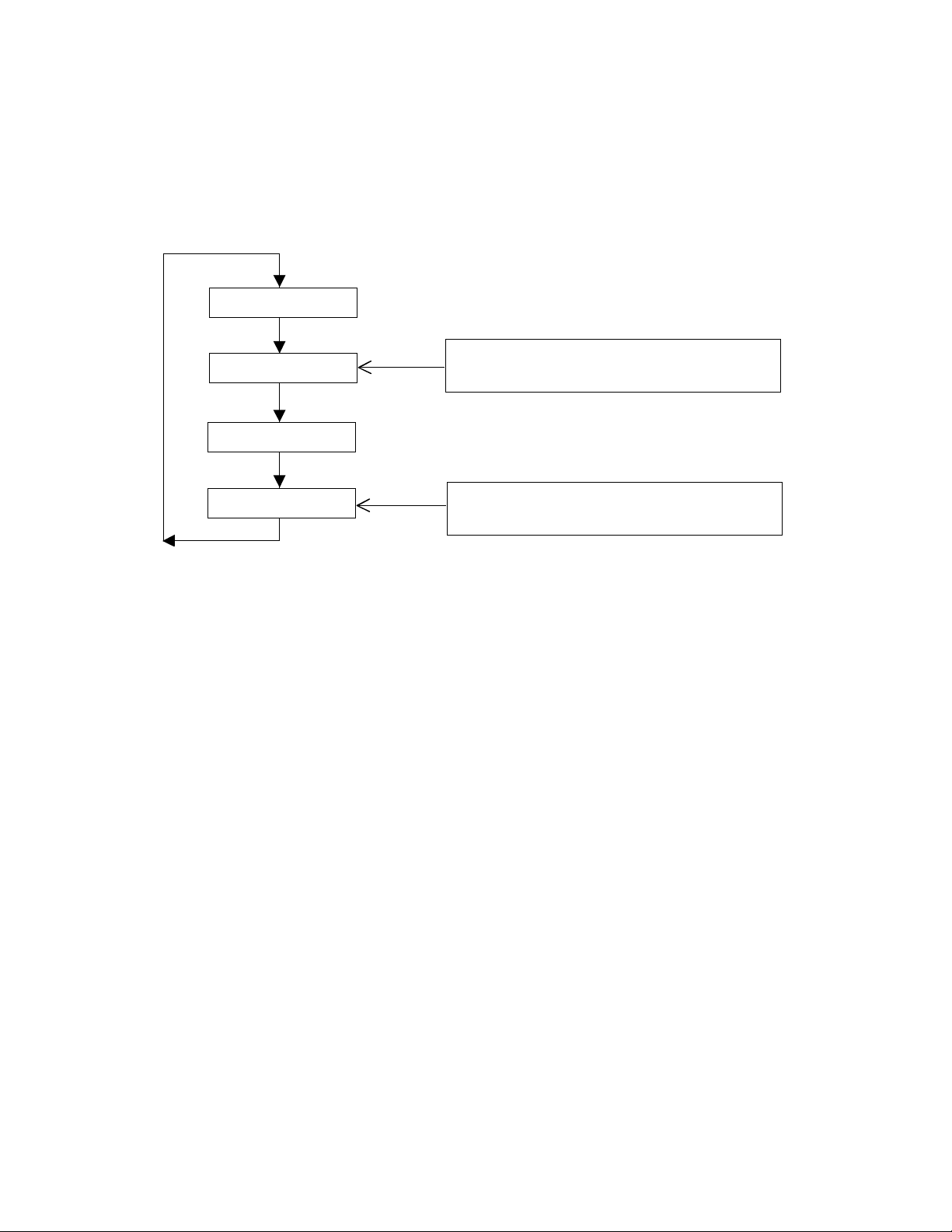
15-1
15-2
CONTROL
PRE-ADJUST
REQUIREMENT
CONTENT
INPUT
CONDITION
OUTPUT
ADJUSTMENT
PROCEDURE
HISTORY
OF REVISION
BUS OPTION FOR THIRD STAGE SERVICE DATA
FUNCTION
001 002 003 004 005 006 007 008 009 010
DEMO DOWNLOAD V-CHIP SP FAO P.PREF UNIV+ VIEW EZ PON-CH
21FL94 1 0 0 1 1 1 1 1 0 0
DEF “0”=DISABLE “1”=ENABLE
009 → “0”=EZ-SETUP “1”=AUTO PRESET
BUS OPTION FOR THIRD STAGE SERVICE DATA
FUNCTION
011 012 013 014 015 016 017 018 019 020
FAV-COL COMP AV AV2 MTS TONE AUTO LAN SETUP AV-FR
21FL94 1 1 1 1 1 1 1 1 1 3
OPTION SET UP
REFER AS BELOW STEP RANGE REFER AS BELOW
–
–
–
21FL94
OSD CHECKING
FUNCTION
021 022 023 024 025 026 027 028 029 030
AV3 COMB A-IN
CLOCK
LED FLAT BASS DSE SRS WHITE
21FL94 0 0 1 1 0 1 0 0 0 0
DEF 011 → ”0”=FAV-COL “1”=COL-TEMP
018 → “0”=ENGLISH “1”=SPANISH
019 → “0”=NO SET UP “1”=AUTO SETUP
025 → “0”=SEMEX SPEC “1”=SPC SPEC
SYMBOL REVISED CONTENT,
DATA SETUP FOR FIRST AND SECOND STAGE SERVICE DATA
DATA SETUP FOR FIRST AND SECOND STAGE SERVICE DATA
BUS SET UP
REFER AS BELOW STEP RANGE REFER AS BELOW
–
–
–
21FL94
OSD CHECKING
ADJUSTMENT
ITEM
ADJUSTMENT
POSITION
CONTROL
PRE-ADJUST
REQUIREMENT
CONTENT
INPUT
CONDITION
OUTPUT
ADJUSTMENT
PROCEDURE
HISTORY
OF REVISION
FUNCTION
V05 F15 F16 F19 F21 F23 F24 F25 F26 F27 F28
SHARP Y-DL(TV) Y-DL(AV) TINT-AV COL-AV R-D(R2) R-D(R) R-D(B)
B-D(R2)
B-D(R) B-D(B)
21FL94 50 5 2 -7 4 +8 +3 -2 -18 -8 +6
DEF
FUNCTION
F30 F35 F39 F40 F44 F46 F47 F56 F57 F60 F61
GAMMA 1W(AV) SL(TV) SL(AV) VD(TV) AS(TV)
AS(AV) FAO-VOL CP
C-OF
TINT-OF
21FL94 1 1 1 1 1 1 1 58 1 +10 +8
ADJUSTMENT
POSITION
ADJUSTMENT
ITEM
FUNCTION
F62 F66 F67
TI-YUV
G-C-YUV
B-C-YUV
21FL94 -12 +36 +2
DEF
SYMBOL REVISED CONTENT,
 Loading...