


 Loading...
C8051F320/1
Full Speed USB, 16 k ISP FLASH MCU Family
Analog Peripherals
-10-Bit ADC
•Up to 200 ksps
•Up to 17 or 13 external single-ended or differential inputs
•VREF from external pin, internal reference, or VDD
•Built-in temperature sensor
•External conversion start input
-Two Comparators
-Internal Voltage Reference
-POR/Brown-Out Detector
USB Function Controller
-USB specification 2.0 compliant
-Full speed (12 Mbps) or low speed (1.5 Mbps) operation
-Integrated clock recovery; no external crystal required for full speed or low speed
-Supports eight flexible endpoints
-1 kB USB buffer memory
-Integrated transceiver; no external resistors required
On-Chip Debug
-On-chip debug circuitry facilitates full speed, non-intrusive in-system debug (no emulator required)
-Provides breakpoints, single stepping, inspect/modify memory and registers
-Superior performance to emulation systems using ICE-chips, target pods, and sockets
Voltage Regulator Input: 4.0 to 5.25 V
High Speed 8051 µC Core
-Pipelined instruction architecture; executes 70% of instructions in 1 or 2 system clocks
-Up to 25 MIPS throughput with 25 MHz clock
-Expanded interrupt handler
Memory
-2304 bytes internal RAM (1k + 256 + 1k USB FIFO)
-16 kB Flash; In-system programmable in 512-byte sectors
Digital Peripherals
-25/21 Port I/O; All 5 V tolerant with high sink current
-Hardware enhanced SPI™, enhanced UART, and SMBus™ serial ports
-Four general purpose 16-bit counter/timers
-16-bit programmable counter array (PCA) with five capture/compare modules
-Real time clock mode using external clock source and PCA or timer
Clock Sources
-Internal Oscillator: 0.25% accuracy with clock recovery enabled. Supports all USB and UART modes
-External oscillator: Crystal, RC, C, or Clock (1 or 2 pin modes)
-Can switch between clock sources on-the-fly; useful in power saving strategies
RoHS Compliant Packages
-32-pin LQFP (C8051F320)
-28-pin QFN (C8051F321)
Temperature Range: –40 to +85 °C
ANALOG
PERIPHERALS
A |
10-bit |
+ |
|
|
|||
M |
200 ksps |
- |
|
U |
|||
ADC |
+ |
||
X |
- |
||
|
|
TEMP |
VREF |
VREG |
|
SENSOR |
|||
|
|
PRECISION INTERNAL
OSCILLATOR
DIGITAL I/O
UART |
CROSSBAR |
Port 0 |
|
SPI |
|||
|
|||
SMBus |
Port 1 |
||
PCA |
Port 2 |
||
Timer 0 |
|||
|
|
||
Timer 1 |
|
Port 3 |
|
Timer 2 |
|
||
|
|
||
Timer 3 |
|
|
USB Controller /
Transceiver
HIGH-SPEED CONTROLLER CORE
16 kB |
8051 CPU |
2304 B |
||
ISP FLASH |
(25MIPS) |
SRAM |
||
16 |
DEBUG |
POR |
WDT |
|
INTERRUPTS |
CIRCUITRY |
|||
|
|
|||
Rev. 1.2 6/07 |
Copyright © 2007 by Silicon Laboratories |
C8051F32x |
This information applies to a product under development. Its characteristics and specifications are subject to change without notice.

C8051F320/1
2 |
Rev. 1.2 |

|
|
C8051F320/1 |
Table of Contents |
|
|
1. |
System Overview.................................................................................................... |
15 |
|
1.1. CIP-51™ Microcontroller Core.......................................................................... |
18 |
|
1.1.1. Fully 8051 Compatible.............................................................................. |
18 |
|
1.1.2. Improved Throughput............................................................................... |
18 |
|
1.1.3. Additional Features .................................................................................. |
18 |
|
1.2. On-Chip Memory............................................................................................... |
19 |
|
1.3. Universal Serial Bus Controller ......................................................................... |
20 |
|
1.4. Voltage Regulator ............................................................................................. |
21 |
|
1.5. On-Chip Debug Circuitry................................................................................... |
21 |
|
1.6. Programmable Digital I/O and Crossbar ........................................................... |
22 |
|
1.7. Serial Ports ....................................................................................................... |
23 |
|
1.8. Programmable Counter Array ........................................................................... |
23 |
|
1.9. 10-Bit Analog to Digital Converter..................................................................... |
24 |
|
1.10.Comparators..................................................................................................... |
25 |
2. |
Absolute Maximum Ratings .................................................................................. |
27 |
3. |
Global Electrical Characteristics .......................................................................... |
28 |
4. Pinout and Package Definitions............................................................................ |
30 |
|
5. |
10-Bit ADC (ADC0).................................................................................................. |
38 |
|
5.1. Analog Multiplexer ............................................................................................ |
39 |
|
5.2. Temperature Sensor ......................................................................................... |
40 |
|
5.3. Modes of Operation .......................................................................................... |
42 |
|
5.3.1. Starting a Conversion............................................................................... |
42 |
|
5.3.2. Tracking Modes........................................................................................ |
43 |
|
5.3.3. Settling Time Requirements ..................................................................... |
44 |
|
5.4. Programmable Window Detector ...................................................................... |
49 |
|
5.4.1. Window Detector In Single-Ended Mode ................................................. |
51 |
|
5.4.2. Window Detector In Differential Mode...................................................... |
52 |
6. |
Voltage Reference .................................................................................................. |
54 |
7. |
Comparators ......................................................................................................... |
56 |
8. |
Voltage Regulator (REG0)...................................................................................... |
66 |
|
8.1. Regulator Mode Selection................................................................................. |
66 |
|
8.2. VBUS Detection ................................................................................................ |
66 |
9. |
CIP-51 Microcontroller .......................................................................................... |
70 |
|
9.1. Instruction Set ................................................................................................... |
71 |
|
9.1.1. Instruction and CPU Timing ..................................................................... |
71 |
|
9.1.2. MOVX Instruction and Program Memory ................................................. |
72 |
|
9.2. Memory Organization........................................................................................ |
76 |
|
9.2.1. Program Memory...................................................................................... |
76 |
|
9.2.2. Data Memory............................................................................................ |
77 |
|
9.2.3. General Purpose Registers ...................................................................... |
77 |
|
9.2.4. Bit Addressable Locations........................................................................ |
77 |
|
9.2.5. Stack ....................................................................................................... |
77 |
|
9.2.6. Special Function Registers....................................................................... |
78 |
Rev. 1.2 |
3 |

C8051F320/1 |
|
9.2.7. Register Descriptions ............................................................................... |
82 |
9.3. Interrupt Handler ............................................................................................... |
86 |
9.3.1. MCU Interrupt Sources and Vectors ........................................................ |
86 |
9.3.2. External Interrupts .................................................................................... |
87 |
9.3.3. Interrupt Priorities..................................................................................... |
87 |
9.3.4. Interrupt Latency ...................................................................................... |
88 |
9.3.5. Interrupt Register Descriptions................................................................. |
89 |
9.4. Power Management Modes .............................................................................. |
96 |
9.4.1. Idle Mode.................................................................................................. |
96 |
9.4.2. Stop Mode................................................................................................ |
96 |
10.Reset Sources ....................................................................................................... |
98 |
10.1.Power-On Reset ............................................................................................... |
99 |
10.2.Power-Fail Reset / VDD Monitor .................................................................... |
100 |
10.3.External Reset................................................................................................ |
101 |
10.4.Missing Clock Detector Reset ........................................................................ |
101 |
10.5.Comparator0 Reset ........................................................................................ |
101 |
10.6.PCA Watchdog Timer Reset .......................................................................... |
101 |
10.7.Flash Error Reset ........................................................................................... |
101 |
10.8.Software Reset............................................................................................... |
102 |
10.9.USB Reset...................................................................................................... |
102 |
11.Flash Memory ..................................................................................................... |
105 |
11.1.Programming The Flash Memory ................................................................... |
105 |
11.1.1.Flash Lock and Key Functions............................................................... |
105 |
11.1.2.Flash Erase Procedure .......................................................................... |
105 |
11.1.3.Flash Write Procedure ........................................................................... |
106 |
11.2.Non-volatile Data Storage .............................................................................. |
106 |
11.3.Security Options ............................................................................................. |
107 |
11.4.Flash Write and Erase Guidelines .................................................................. |
109 |
11.4.1.VDD Maintenance and the VDD Monitor ............................................... |
109 |
11.4.2.16.4.2 PSWE Maintenance.................................................................... |
110 |
11.4.3.System Clock ......................................................................................... |
110 |
12.External RAM ...................................................................................................... |
113 |
12.1.Accessing User XRAM ................................................................................... |
113 |
12.2.Accessing USB FIFO Space .......................................................................... |
113 |
13.Oscillators............................................................................................................. |
115 |
13.1.Programmable Internal Oscillator ................................................................... |
115 |
13.1.1.Programming the Internal Oscillator on C8051F320/1 Devices............. |
116 |
13.1.2.Internal Oscillator Suspend Mode.......................................................... |
117 |
13.2.External Oscillator Drive Circuit...................................................................... |
118 |
13.2.1.Clocking Timers Directly Through the External Oscillator...................... |
118 |
13.2.2.External Crystal Example....................................................................... |
118 |
13.2.3.External RC Example............................................................................. |
119 |
13.2.4.External Capacitor Example................................................................... |
119 |
13.3.4x Clock Multiplier .......................................................................................... |
121 |
13.4.System and USB Clock Selection .................................................................. |
122 |
4 |
Rev. 1.2 |

|
C8051F320/1 |
13.4.1.System Clock Selection ......................................................................... |
122 |
13.4.2.USB Clock Selection.............................................................................. |
122 |
14.Port Input/Output ................................................................................................ |
125 |
14.1.Priority Crossbar Decoder .............................................................................. |
127 |
14.2.Port I/O Initialization ....................................................................................... |
129 |
14.3.General Purpose Port I/O ............................................................................... |
131 |
15.Universal Serial Bus Controller (USB)................................................................ |
138 |
15.1.Endpoint Addressing ...................................................................................... |
139 |
15.2.USB Transceiver ............................................................................................ |
139 |
15.3.USB Register Access ..................................................................................... |
141 |
15.4.USB Clock Configuration................................................................................ |
145 |
15.5.FIFO Management ......................................................................................... |
146 |
15.5.1.FIFO Split Mode..................................................................................... |
146 |
15.5.2.FIFO Double Buffering ........................................................................... |
147 |
15.5.3.FIFO Access .......................................................................................... |
147 |
15.6.Function Addressing....................................................................................... |
148 |
15.7.Function Configuration and Control................................................................ |
148 |
15.8.Interrupts ........................................................................................................ |
151 |
15.9.The Serial Interface Engine............................................................................ |
156 |
15.10.Endpoint0 ..................................................................................................... |
156 |
15.10.1.Endpoint0 SETUP Transactions .......................................................... |
157 |
15.10.2.Endpoint0 IN Transactions................................................................... |
157 |
15.10.3.Endpoint0 OUT Transactions............................................................... |
158 |
15.11.Configuring Endpoints1–3 ............................................................................ |
160 |
15.12.Controlling Endpoints1–3 IN......................................................................... |
161 |
15.12.1.Endpoints1-3 IN Interrupt or Bulk Mode............................................... |
161 |
15.12.2.Endpoints1-3 IN Isochronous Mode..................................................... |
161 |
15.13.Controlling Endpoints1–3 OUT..................................................................... |
164 |
15.13.1.Endpoints1-3 OUT Interrupt or Bulk Mode........................................... |
164 |
15.13.2.Endpoints1-3 OUT Isochronous Mode................................................. |
165 |
16.SMBus ................................................................................................................... |
169 |
16.1.Supporting Documents................................................................................... |
170 |
16.2.SMBus Configuration...................................................................................... |
170 |
16.3.SMBus Operation ........................................................................................... |
170 |
16.3.1.Arbitration............................................................................................... |
171 |
16.3.2.Clock Low Extension.............................................................................. |
171 |
16.3.3.SCL Low Timeout................................................................................... |
171 |
16.3.4.SCL High (SMBus Free) Timeout .......................................................... |
172 |
16.4.Using the SMBus............................................................................................ |
172 |
16.4.1.SMBus Configuration Register............................................................... |
173 |
16.4.2.SMB0CN Control Register ..................................................................... |
176 |
16.4.3.Data Register ......................................................................................... |
179 |
16.5.SMBus Transfer Modes.................................................................................. |
180 |
16.5.1.Master Transmitter Mode....................................................................... |
180 |
16.5.2.Master Receiver Mode........................................................................... |
181 |
Rev. 1.2 |
5 |

C8051F320/1 |
|
16.5.3.Slave Receiver Mode............................................................................. |
182 |
16.5.4.Slave Transmitter Mode......................................................................... |
183 |
16.6.SMBus Status Decoding................................................................................. |
184 |
17.UART0.................................................................................................................... |
187 |
17.1.Enhanced Baud Rate Generation................................................................... |
188 |
17.2.Operational Modes ......................................................................................... |
188 |
17.2.1.8-Bit UART............................................................................................. |
189 |
17.2.2.9-Bit UART............................................................................................. |
190 |
17.3.Multiprocessor Communications .................................................................... |
190 |
18.Enhanced Serial Peripheral Interface (SPI0)...................................................... |
195 |
18.1.Signal Descriptions......................................................................................... |
196 |
18.1.1.Master Out, Slave In (MOSI).................................................................. |
196 |
18.1.2.Master In, Slave Out (MISO).................................................................. |
196 |
18.1.3.Serial Clock (SCK) ................................................................................. |
196 |
18.1.4.Slave Select (NSS) ................................................................................ |
196 |
18.2.SPI0 Master Mode Operation......................................................................... |
197 |
18.3.SPI0 Slave Mode Operation ........................................................................... |
198 |
18.4.SPI0 Interrupt Sources ................................................................................... |
199 |
18.5.Serial Clock Timing......................................................................................... |
199 |
18.6.SPI Special Function Registers ...................................................................... |
202 |
19.Timers ................................................................................................................... |
209 |
19.1.Timer 0 and Timer 1 ....................................................................................... |
209 |
19.1.1.Mode 0: 13-bit Counter/Timer ................................................................ |
209 |
19.1.2.Mode 1: 16-bit Counter/Timer ................................................................ |
211 |
19.1.3.Mode 2: 8-bit Counter/Timer with Auto-Reload...................................... |
211 |
19.1.4.Mode 3: Two 8-bit Counter/Timers (Timer 0 Only)................................. |
212 |
19.2.Timer 2 .......................................................................................................... |
217 |
19.2.1.16-bit Timer with Auto-Reload................................................................ |
217 |
19.2.2.8-bit Timers with Auto-Reload................................................................ |
218 |
19.2.3.USB Start-of-Frame Capture.................................................................. |
219 |
19.3.Timer 3 .......................................................................................................... |
222 |
19.3.1.16-bit Timer with Auto-Reload................................................................ |
222 |
19.3.2.8-bit Timers with Auto-Reload................................................................ |
223 |
19.3.3.USB Start-of-Frame Capture.................................................................. |
224 |
20.Programmable Counter Array (PCA0) ................................................................ |
227 |
20.1.PCA Counter/Timer ........................................................................................ |
228 |
20.2.Capture/Compare Modules ............................................................................ |
229 |
20.2.1.Edge-triggered Capture Mode................................................................ |
230 |
20.2.2.Software Timer (Compare) Mode........................................................... |
232 |
20.2.3.High Speed Output Mode....................................................................... |
233 |
20.2.4.Frequency Output Mode ........................................................................ |
234 |
20.2.5.8-Bit Pulse Width Modulator Mode......................................................... |
235 |
20.2.6.16-Bit Pulse Width Modulator Mode....................................................... |
236 |
20.3.Watchdog Timer Mode ................................................................................... |
236 |
20.3.1.Watchdog Timer Operation.................................................................... |
237 |
6 |
Rev. 1.2 |

|
C8051F320/1 |
20.3.2.Watchdog Timer Usage ......................................................................... |
238 |
20.4.Register Descriptions for PCA........................................................................ |
239 |
21.C2 Interface ........................................................................................................... |
245 |
21.1.C2 Interface Registers.................................................................................... |
245 |
21.2.C2 Pin Sharing ............................................................................................... |
247 |
Rev. 1.2 |
7 |

C8051F320/1 |
|
|
List of Figures and Tables |
|
|
1. |
System Overview |
|
|
Table 1.1. Product Selection Guide ........................................................................ |
16 |
|
Figure 1.1. C8051F320 Block Diagram .................................................................... |
16 |
|
Figure 1.2. C8051F321 Block Diagram .................................................................... |
17 |
|
Figure 1.3. On-Chip Clock and Reset ...................................................................... |
19 |
|
Figure 1.4. On-Board Memory Map.......................................................................... |
20 |
|
Figure 1.5. USB Controller Block Diagram............................................................... |
21 |
|
Figure 1.6. Development/In-System Debug Diagram............................................... |
22 |
|
Figure 1.7. Digital Crossbar Diagram ....................................................................... |
23 |
|
Figure 1.8. PCA Block Diagram ............................................................................... |
24 |
|
Figure 1.9. PCA Block Diagram ............................................................................... |
24 |
|
Figure 1.10. 10-Bit ADC Block Diagram ................................................................... |
25 |
|
Figure 1.11. Comparator0 Block Diagram ................................................................ |
26 |
2. |
Absolute Maximum Ratings |
|
|
Table 2.1. Absolute Maximum Ratings .................................................................... |
27 |
3. |
Global Electrical Characteristics |
|
|
Table 3.1. Global Electrical Characteristics ............................................................. |
28 |
|
Table 3.2. Index to Electrical Characteristics Tables .............................................. |
29 |
4. Pinout and Package Definitions |
|
|
|
Table 4.1. Pin Definitions for the C8051F320/1 ...................................................... |
30 |
|
Figure 4.1. LQFP-32 Pinout Diagram (Top View) .................................................... |
32 |
|
Figure 4.2. LQFP-32 Package Diagram ................................................................... |
33 |
|
Table 4.2. LQFP-32 Package Dimensions.............................................................. |
33 |
|
Figure 4.3. QFN-28 Pinout Diagram (Top View) ...................................................... |
34 |
|
Figure 4.4. QFN-28 Package Drawing ..................................................................... |
35 |
|
Table 4.3. QFN-28 Package Dimensions................................................................ |
35 |
|
Figure 4.5. Typical QFN-28 Landing Diagram.......................................................... |
36 |
|
Figure 4.6. QFN-28 Solder Paste Recommendation................................................ |
37 |
5. |
10-Bit ADC (ADC0) |
|
|
Figure 5.1. ADC0 Functional Block Diagram............................................................ |
38 |
|
Figure 5.2. Temperature Sensor Transfer Function ................................................. |
40 |
|
Figure 5.3. Temperature Sensor Error with 1-Point Calibration (VREF = 2.40 V).... |
41 |
|
Figure 5.4. 10-Bit ADC Track and Conversion Example Timing .............................. |
43 |
|
Figure 5.5. ADC0 Equivalent Input Circuits.............................................................. |
44 |
|
Figure 5.6. ADC Window Compare Example: Right-Justified Single-Ended Data ... |
51 |
|
Figure 5.7. ADC Window Compare Example: Left-Justified Single-Ended Data ..... |
51 |
|
Figure 5.8. ADC Window Compare Example: Right-Justified Differential Data ....... |
52 |
|
Figure 5.9. ADC Window Compare Example: Left-Justified Differential Data.......... |
52 |
|
Table 5.1. ADC0 Electrical Characteristics ............................................................. |
53 |
6. |
Voltage Reference |
|
|
Figure 6.1. Voltage Reference Functional Block Diagram ....................................... |
54 |
|
Table 6.1. Voltage Reference Electrical Characteristics ......................................... |
55 |
8 |
Rev. 1.2 |

|
C8051F320/1 |
|
7. |
Comparators |
|
|
Figure 7.1. Comparator0 Functional Block Diagram ................................................ |
56 |
|
Figure 7.2. Comparator1 Functional Block Diagram ................................................ |
57 |
|
Figure 7.3. Comparator Hysteresis Plot ................................................................... |
58 |
|
Table 7.1. Comparator Electrical Characteristics .................................................... |
65 |
8. |
Voltage Regulator (REG0) |
|
|
Figure 8.1. External Capacitors for Voltage Regulator Input/Output ........................ |
66 |
|
Table 8.1. Voltage Regulator Electrical Specifications ............................................ |
67 |
|
Figure 8.2. REG0 Configuration: USB Bus-Powered ............................................... |
67 |
|
Figure 8.3. REG0 Configuration: USB Self-Powered ............................................... |
68 |
|
Figure 8.4. REG0 Configuration: USB Self-Powered, Regulator Disabled .............. |
68 |
|
Figure 8.5. REG0 Configuration: No USB Connection............................................. |
69 |
9. |
CIP-51 Microcontroller |
|
|
Figure 9.1. CIP-51 Block Diagram............................................................................ |
70 |
|
Table 9.1. CIP-51 Instruction Set Summary............................................................ |
72 |
|
Figure 9.2. Memory Map .......................................................................................... |
76 |
|
Table 9.2. Special Function Register (SFR) Memory Map...................................... |
78 |
|
Table 9.3. Special Function Registers .................................................................... |
79 |
|
Table 9.4. Interrupt Summary ................................................................................. |
88 |
10.Reset Sources |
|
|
|
Figure 10.1. Reset Sources...................................................................................... |
98 |
|
Figure 10.2. Power-On and VDD Monitor Reset Timing .......................................... |
99 |
|
Table 10.1. Reset Electrical Characteristics .......................................................... |
104 |
11.Flash Memory |
|
|
|
Table 11.1. Flash Electrical Characteristics .......................................................... |
106 |
|
Figure 11.1. Flash Program Memory Map and Security Byte................................. |
107 |
|
Table 11.2. Flash Security Summary ..................................................................... |
108 |
12.External RAM |
|
|
|
Figure 12.1. External Ram Memory Map................................................................ |
113 |
|
Figure 12.2. XRAM Memory Map Expanded View ................................................. |
114 |
13.Oscillators |
|
|
|
Figure 13.1. Oscillator Diagram.............................................................................. |
115 |
|
Table 13.1. Typical USB Full Speed Clock Settings............................................... |
122 |
|
Table 13.2. Typical USB Low Speed Clock Settings.............................................. |
123 |
|
Table 13.3. Internal Oscillator Electrical Characteristics ....................................... |
124 |
14.Port Input/Output |
|
|
|
Figure 14.1. Port I/O Functional Block Diagram ..................................................... |
125 |
|
Figure 14.2. Port I/O Cell Block Diagram ............................................................... |
126 |
|
Figure 14.3. Crossbar Priority Decoder with No Pins Skipped ............................... |
127 |
|
Figure 14.4. Crossbar Priority Decoder with Crystal Pins Skipped ........................ |
128 |
|
Table 14.1. Port I/O DC Electrical Characteristics ................................................ |
137 |
15.Universal Serial Bus Controller (USB) |
|
|
|
Figure 15.1. USB0 Block Diagram.......................................................................... |
138 |
|
Table 15.1. Endpoint Addressing Scheme ............................................................. |
139 |
|
Figure 15.2. USB0 Register Access Scheme......................................................... |
141 |
Rev. 1.2 |
9 |

C8051F320/1 |
|
Table 15.2. USB0 Controller Registers .................................................................. |
143 |
Figure 15.3. USB FIFO Allocation .......................................................................... |
146 |
Table 15.3. FIFO Configurations ............................................................................ |
147 |
Table 15.4. USB Transceiver Electrical Characteristics ........................................ |
168 |
16.SMBus |
|
Figure 16.1. SMBus Block Diagram ....................................................................... |
169 |
Figure 16.2. Typical SMBus Configuration ............................................................. |
170 |
Figure 16.3. SMBus Transaction ............................................................................ |
171 |
Table 16.1. SMBus Clock Source Selection........................................................... |
173 |
Figure 16.4. Typical SMBus SCL Generation......................................................... |
174 |
Table 16.2. Minimum SDA Setup and Hold Times ................................................. |
174 |
Table 16.3. Sources for Hardware Changes to SMB0CN ...................................... |
178 |
Figure 16.5. Typical Master Transmitter Sequence................................................ |
180 |
Figure 16.6. Typical Master Receiver Sequence.................................................... |
181 |
Figure 16.7. Typical Slave Receiver Sequence...................................................... |
182 |
Figure 16.8. Typical Slave Transmitter Sequence.................................................. |
183 |
Table 16.4. SMBus Status Decoding...................................................................... |
184 |
17.UART0 |
|
Figure 17.1. UART0 Block Diagram ....................................................................... |
187 |
Figure 17.2. UART0 Baud Rate Logic .................................................................... |
188 |
Figure 17.3. UART Interconnect Diagram .............................................................. |
189 |
Figure 17.4. 8-Bit UART Timing Diagram............................................................... |
189 |
Figure 17.5. 9-Bit UART Timing Diagram............................................................... |
190 |
Figure 17.6. UART Multi-Processor Mode Interconnect Diagram .......................... |
191 |
Table 17.1. Timer Settings for Standard Baud Rates Using The Internal Oscillator 194 |
|
18.Enhanced Serial Peripheral Interface (SPI0) |
|
Figure 18.1. SPI Block Diagram ............................................................................. |
195 |
Figure 18.2. Multiple-Master Mode Connection Diagram ....................................... |
198 |
Figure 18.3. 3-Wire Single Master and Slave Mode Connection Diagram ............. |
198 |
Figure 18.4. 4-Wire Single Master Mode and 4-Wire |
|
Slave Mode Connection Diagram ....................................................... |
198 |
Figure 18.5. Master Mode Data/Clock Timing ........................................................ |
200 |
Figure 18.6. Slave Mode Data/Clock Timing (CKPHA = 0) .................................... |
200 |
Figure 18.7. Slave Mode Data/Clock Timing (CKPHA = 1) .................................... |
201 |
Figure 18.8. SPI Master Timing (CKPHA = 0)........................................................ |
206 |
Figure 18.9. SPI Master Timing (CKPHA = 1)........................................................ |
206 |
Figure 18.10. SPI Slave Timing (CKPHA = 0)........................................................ |
207 |
Figure 18.11. SPI Slave Timing (CKPHA = 1)........................................................ |
207 |
Table 18.1. SPI Slave Timing Parameters ............................................................. |
208 |
19.Timers |
|
Figure 19.1. T0 Mode 0 Block Diagram.................................................................. |
210 |
Figure 19.2. T0 Mode 2 Block Diagram.................................................................. |
211 |
Figure 19.3. T0 Mode 3 Block Diagram.................................................................. |
212 |
Figure 19.4. Timer 2 16-Bit Mode Block Diagram .................................................. |
217 |
Figure 19.5. Timer 2 8-Bit Mode Block Diagram .................................................... |
218 |
10 |
Rev. 1.2 |
C8051F320/1 |
|
Figure 19.6. Timer 2 SOF Capture Mode (T2SPLIT = ‘0’)...................................... |
219 |
Figure 19.7. Timer 2 SOF Capture Mode (T2SPLIT = ‘1’)...................................... |
219 |
Figure 19.8. Timer 3 16-Bit Mode Block Diagram .................................................. |
222 |
Figure 19.9. Timer 3 8-Bit Mode Block Diagram .................................................... |
223 |
Figure 19.10. Timer 3 SOF Capture Mode (T3SPLIT = ‘0’).................................... |
224 |
Figure 19.11. Timer 3 SOF Capture Mode (T3SPLIT = ‘1’).................................... |
224 |
20.Programmable Counter Array (PCA0) |
|
Figure 20.1. PCA Block Diagram............................................................................ |
227 |
Table 20.1. PCA Timebase Input Options .............................................................. |
228 |
Figure 20.2. PCA Counter/Timer Block Diagram.................................................... |
228 |
Table 20.2. PCA0CPM Register Settings for PCA Capture/Compare Modules ..... |
229 |
Figure 20.3. PCA Interrupt Block Diagram ............................................................. |
230 |
Figure 20.4. PCA Capture Mode Diagram.............................................................. |
231 |
Figure 20.5. PCA Software Timer Mode Diagram .................................................. |
232 |
Figure 20.6. PCA High Speed Output Mode Diagram............................................ |
233 |
Figure 20.7. PCA Frequency Output Mode ............................................................ |
234 |
Figure 20.8. PCA 8-Bit PWM Mode Diagram ......................................................... |
235 |
Figure 20.9. PCA 16-Bit PWM Mode...................................................................... |
236 |
Figure 20.10. PCA Module 4 with Watchdog Timer Enabled ................................. |
237 |
Table 20.3. Watchdog Timer Timeout Intervals...................................................... |
239 |
21.C2 Interface |
|
Figure 21.1. Typical C2 Pin Sharing....................................................................... |
247 |
Rev. 1.2 |
11 |

C8051F320/1 |
|
List of Registers |
|
SFR Definition 5.1. AMX0P: AMUX0 Positive Channel Select . . . . . . . . . . . . . . . . . |
. 45 |
SFR Definition 5.2. AMX0N: AMUX0 Negative Channel Select . . . . . . . . . . . . . . . . . |
. 46 |
SFR Definition 5.3. ADC0CF: ADC0 Configuration . . . . . . . . . . . . . . . . . . . . . . . . . . |
. 47 |
SFR Definition 5.4. ADC0H: ADC0 Data Word MSB . . . . . . . . . . . . . . . . . . . . . . . . . |
. 47 |
SFR Definition 5.5. ADC0L: ADC0 Data Word LSB . . . . . . . . . . . . . . . . . . . . . . . . . . |
. 47 |
SFR Definition 5.6. ADC0CN: ADC0 Control . . . . . . . . . . . . . . . . . . . . . . . . . . . . . . . |
. 48 |
SFR Definition 5.7. ADC0GTH: ADC0 Greater-Than Data High Byte . . . . . . . . . . . . |
. 49 |
SFR Definition 5.8. ADC0GTL: ADC0 Greater-Than Data Low Byte . . . . . . . . . . . . |
. 49 |
SFR Definition 5.9. ADC0LTH: ADC0 Less-Than Data High Byte . . . . . . . . . . . . . . . |
. 50 |
SFR Definition 5.10. ADC0LTL: ADC0 Less-Than Data Low Byte . . . . . . . . . . . . . . |
. 50 |
SFR Definition 6.1. REF0CN: Reference Control . . . . . . . . . . . . . . . . . . . . . . . . . . . . |
. 55 |
SFR Definition 7.1. CPT0CN: Comparator0 Control . . . . . . . . . . . . . . . . . . . . . . . . . . |
. 59 |
SFR Definition 7.2. CPT0MX: Comparator0 MUX Selection . . . . . . . . . . . . . . . . . . . |
. 60 |
SFR Definition 7.3. CPT0MD: Comparator0 Mode Selection . . . . . . . . . . . . . . . . . . . |
. 61 |
SFR Definition 7.4. CPT1CN: Comparator1 Control . . . . . . . . . . . . . . . . . . . . . . . . . . |
. 62 |
SFR Definition 7.5. CPT1MX: Comparator1 MUX Selection . . . . . . . . . . . . . . . . . . . |
. 63 |
SFR Definition 7.6. CPT1MD: Comparator1 Mode Selection . . . . . . . . . . . . . . . . . . . |
. 64 |
SFR Definition 8.1. REG0CN: Voltage Regulator Control . . . . . . . . . . . . . . . . . . . . . |
. 69 |
SFR Definition 9.1. DPL: Data Pointer Low Byte . . . . . . . . . . . . . . . . . . . . . . . . . . . . |
. 82 |
SFR Definition 9.2. DPH: Data Pointer High Byte . . . . . . . . . . . . . . . . . . . . . . . . . . . . |
. 83 |
SFR Definition 9.3. SP: Stack Pointer . . . . . . . . . . . . . . . . . . . . . . . . . . . . . . . . . . . . . |
. 83 |
SFR Definition 9.4. PSW: Program Status Word . . . . . . . . . . . . . . . . . . . . . . . . . . . . |
. 84 |
SFR Definition 9.5. ACC: Accumulator . . . . . . . . . . . . . . . . . . . . . . . . . . . . . . . . . . . . |
. 85 |
SFR Definition 9.6. B: B Register . . . . . . . . . . . . . . . . . . . . . . . . . . . . . . . . . . . . . . . . |
. 85 |
SFR Definition 9.7. IE: Interrupt Enable . . . . . . . . . . . . . . . . . . . . . . . . . . . . . . . . . . . |
. 90 |
SFR Definition 9.8. IP: Interrupt Priority . . . . . . . . . . . . . . . . . . . . . . . . . . . . . . . . . . . |
. 91 |
SFR Definition 9.9. EIE1: Extended Interrupt Enable 1 . . . . . . . . . . . . . . . . . . . . . . . |
. 92 |
SFR Definition 9.10. EIP1: Extended Interrupt Priority 1 . . . . . . . . . . . . . . . . . . . . . . |
. 93 |
SFR Definition 9.11. EIE2: Extended Interrupt Enable 2 . . . . . . . . . . . . . . . . . . . . . . |
. 94 |
SFR Definition 9.12. EIP2: Extended Interrupt Priority 2 . . . . . . . . . . . . . . . . . . . . . . |
. 94 |
SFR Definition 9.13. IT01CF: INT0/INT1 Configuration . . . . . . . . . . . . . . . . . . . . . . . |
. 95 |
SFR Definition 9.14. PCON: Power Control . . . . . . . . . . . . . . . . . . . . . . . . . . . . . . . . |
. 97 |
SFR Definition 10.1. VDM0CN: VDD Monitor Control . . . . . . . . . . . . . . . . . . . . . . . . |
100 |
SFR Definition 10.2. RSTSRC: Reset Source . . . . . . . . . . . . . . . . . . . . . . . . . . . . . . |
103 |
SFR Definition 11.1. PSCTL: Program Store R/W Control . . . . . . . . . . . . . . . . . . . . . |
111 |
SFR Definition 11.2. FLKEY: Flash Lock and Key . . . . . . . . . . . . . . . . . . . . . . . . . . . |
111 |
SFR Definition 11.3. FLSCL: Flash Scale . . . . . . . . . . . . . . . . . . . . . . . . . . . . . . . . . . |
112 |
SFR Definition 12.1. EMI0CN: External Memory Interface Control . . . . . . . . . . . . . . |
114 |
SFR Definition 13.1. OSCICN: Internal Oscillator Control . . . . . . . . . . . . . . . . . . . . . |
117 |
SFR Definition 13.2. OSCICL: Internal Oscillator Calibration . . . . . . . . . . . . . . . . . . . |
117 |
SFR Definition 13.3. OSCXCN: External Oscillator Control . . . . . . . . . . . . . . . . . . . . |
120 |
SFR Definition 13.4. CLKMUL: Clock Multiplier Control . . . . . . . . . . . . . . . . . . . . . . . |
121 |
SFR Definition 13.5. CLKSEL: Clock Select . . . . . . . . . . . . . . . . . . . . . . . . . . . . . . . . |
123 |
12 |
Rev. 1.2 |

C8051F320/1 |
|
SFR Definition 14.1. XBR0: Port I/O Crossbar Register 0 . . . . . . . . . . . . . . . . . |
. . . . 130 |
SFR Definition 14.2. XBR1: Port I/O Crossbar Register 1 . . . . . . . . . . . . . . . . . . |
. . . 131 |
SFR Definition 14.3. P0: Port0 Register . . . . . . . . . . . . . . . . . . . . . . . . . . . . . . . . |
. . . 132 |
SFR Definition 14.4. P0MDIN: Port0 Input Mode Register . . . . . . . . . . . . . . . . . . |
. . . 132 |
SFR Definition 14.5. P0MDOUT: Port0 Output Mode Register . . . . . . . . . . . . . . |
. . . 132 |
SFR Definition 14.6. P0SKIP: Port0 Skip Register . . . . . . . . . . . . . . . . . . . . . . . . |
. . . 133 |
SFR Definition 14.7. P1: Port1 Register . . . . . . . . . . . . . . . . . . . . . . . . . . . . . . . . |
. . . 133 |
SFR Definition 14.8. P1MDIN: Port1 Input Mode Register . . . . . . . . . . . . . . . . . . |
. . . 133 |
SFR Definition 14.9. P1MDOUT: Port1 Output Mode Register . . . . . . . . . . . . . . |
. . . 134 |
SFR Definition 14.10. P1SKIP: Port1 Skip Register . . . . . . . . . . . . . . . . . . . . . . . |
. . . 134 |
SFR Definition 14.11. P2: Port2 Register . . . . . . . . . . . . . . . . . . . . . . . . . . . . . . . |
. . . 134 |
SFR Definition 14.12. P2MDIN: Port2 Input Mode Register . . . . . . . . . . . . . . . . . |
. . . 135 |
SFR Definition 14.13. P2MDOUT: Port2 Output Mode Register . . . . . . . . . . . . . |
. . . 135 |
SFR Definition 14.14. P2SKIP: Port2 Skip Register . . . . . . . . . . . . . . . . . . . . . . . |
. . . 135 |
SFR Definition 14.15. P3: Port3 Register . . . . . . . . . . . . . . . . . . . . . . . . . . . . . . . |
. . . 136 |
SFR Definition 14.16. P3MDIN: Port3 Input Mode Register . . . . . . . . . . . . . . . . . |
. . . 136 |
SFR Definition 14.17. P3MDOUT: Port3 Output Mode Register . . . . . . . . . . . . . |
. . . 136 |
SFR Definition 15.1. USB0XCN: USB0 Transceiver Control . . . . . . . . . . . . . . . . |
. . . 140 |
SFR Definition 15.2. USB0ADR: USB0 Indirect Address . . . . . . . . . . . . . . . . . . . |
. . . 142 |
SFR Definition 15.3. USB0DAT: USB0 Data . . . . . . . . . . . . . . . . . . . . . . . . . . . . |
. . . 143 |
USB Register Definition 15.4. INDEX: USB0 Endpoint Index . . . . . . . . . . . . . . . . |
. . . 144 |
USB Register Definition 15.5. CLKREC: Clock Recovery Control . . . . . . . . . . . . |
. . . 145 |
USB Register Definition 15.6. FIFOn: USB0 Endpoint FIFO Access . . . . . . . . . . |
. . . 147 |
USB Register Definition 15.7. FADDR: USB0 Function Address . . . . . . . . . . . . . |
. . . 148 |
USB Register Definition 15.8. POWER: USB0 Power . . . . . . . . . . . . . . . . . . . . . |
. . . 150 |
USB Register Definition 15.9. FRAMEL: USB0 Frame Number Low . . . . . . . . . . |
. . . 151 |
USB Register Definition 15.10. FRAMEH: USB0 Frame Number High . . . . . . . . |
. . . 151 |
USB Register Definition 15.11. IN1INT: USB0 IN Endpoint Interrupt . . . . . . . . . |
. . . 152 |
USB Register Definition 15.12. OUT1INT: USB0 Out Endpoint Interrupt . . . . . . . |
. . . 153 |
USB Register Definition 15.13. CMINT: USB0 Common Interrupt . . . . . . . . . . . . |
. . . 154 |
USB Register Definition 15.14. IN1IE: USB0 IN Endpoint Interrupt Enable . . . . . |
. . . 155 |
USB Register Definition 15.15. OUT1IE: USB0 Out Endpoint Interrupt Enable . . . . . 155 |
|
USB Register Definition 15.16. CMIE: USB0 Common Interrupt Enable . . . . . . . |
. . . 156 |
USB Register Definition 15.17. E0CSR: USB0 Endpoint0 Control . . . . . . . . . . . . |
. . . 159 |
USB Register Definition 15.18. E0CNT: USB0 Endpoint 0 Data Count . . . . . . . . |
. . . 160 |
USB Register Definition 15.19. INMAX: USB0 IN Endpoint n Maximum Packet Size 160 |
|
USB Register Definition 15.20. EINCSRL: USB0 IN Endpoint Control Low Byte . |
. . . 163 |
USB Register Definition 15.21. EINCSRH: USB0 IN Endpoint Control High Byte |
. . . 164 |
USB Register Definition 15.22. OUTMAX: USB0 Out Endpoint Max Packet Size |
. . . 165 |
USB Register Definition 15.23. EOUTCSRL: USB0 OUT Endpoint Control High Byte 166 |
|
USB Register Definition 15.24. EOUTCSRH: USB0 OUT Endpoint Control Low Byte 167 |
|
USB Register Definition 15.25. EOUTCNTL: USB0 OUT Endpoint Count Low . . . . . 167 |
|
USB Register Definition 15.26. EOUTCNTH: USB0 OUT Endpoint Count High |
. . . . 167 |
SFR Definition 16.1. SMB0CF: SMBus Clock/Configuration . . . . . . . . . . . . . . . . |
. . . 175 |
SFR Definition 16.2. SMB0CN: SMBus Control . . . . . . . . . . . . . . . . . . . . . . . . . . |
. . . 177 |
Rev. 1.2 |
13 |

C8051F320/1
SFR Definition 16.3. SMB0DAT: SMBus Data . . . . . . . . . . . . . . . . . . . . . . . . . . . . . . 179
SFR Definition 17.1. SCON0: Serial Port 0 Control . . . . . . . . . . . . . . . . . . . . . . . . . . 192
SFR Definition 17.2. SBUF0: Serial (UART0) Port Data Buffer . . . . . . . . . . . . . . . . . 193 SFR Definition 18.1. SPI0CFG: SPI0 Configuration . . . . . . . . . . . . . . . . . . . . . . . . . . 203
SFR Definition 18.2. SPI0CN: SPI0 Control . . . . . . . . . . . . . . . . . . . . . . . . . . . . . . . . 204
SFR Definition 18.3. SPI0CKR: SPI0 Clock Rate . . . . . . . . . . . . . . . . . . . . . . . . . . . . 205 SFR Definition 18.4. SPI0DAT: SPI0 Data Register . . . . . . . . . . . . . . . . . . . . . . . . . . 205
SFR Definition 19.1. TCON: Timer Control . . . . . . . . . . . . . . . . . . . . . . . . . . . . . . . . . 213
SFR Definition 19.2. TMOD: Timer Mode . . . . . . . . . . . . . . . . . . . . . . . . . . . . . . . . . . 214 SFR Definition 19.3. CKCON: Clock Control . . . . . . . . . . . . . . . . . . . . . . . . . . . . . . . 215
SFR Definition 19.4. TL0: Timer 0 Low Byte . . . . . . . . . . . . . . . . . . . . . . . . . . . . . . . . 216
SFR Definition 19.5. TL1: Timer 1 Low Byte . . . . . . . . . . . . . . . . . . . . . . . . . . . . . . . . 216 SFR Definition 19.6. TH0: Timer 0 High Byte . . . . . . . . . . . . . . . . . . . . . . . . . . . . . . . 216
SFR Definition 19.7. TH1: Timer 1 High Byte . . . . . . . . . . . . . . . . . . . . . . . . . . . . . . . 216
SFR Definition 19.8. TMR2CN: Timer 2 Control . . . . . . . . . . . . . . . . . . . . . . . . . . . . . 220
SFR Definition 19.9. TMR2RLL: Timer 2 Reload Register Low Byte . . . . . . . . . . . . . 221
SFR Definition 19.10. TMR2RLH: Timer 2 Reload Register High Byte . . . . . . . . . . . 221 SFR Definition 19.11. TMR2L: Timer 2 Low Byte . . . . . . . . . . . . . . . . . . . . . . . . . . . . 221
SFR Definition 19.12. TMR2H Timer 2 High Byte . . . . . . . . . . . . . . . . . . . . . . . . . . . . 221
SFR Definition 19.13. TMR3CN: Timer 3 Control . . . . . . . . . . . . . . . . . . . . . . . . . . . . 225 SFR Definition 19.14. TMR3RLL: Timer 3 Reload Register Low Byte . . . . . . . . . . . . 226
SFR Definition 19.15. TMR3RLH: Timer 3 Reload Register High Byte . . . . . . . . . . . 226
SFR Definition 19.16. TMR3L: Timer 3 Low Byte . . . . . . . . . . . . . . . . . . . . . . . . . . . . 226 SFR Definition 19.17. TMR3H Timer 3 High Byte . . . . . . . . . . . . . . . . . . . . . . . . . . . . 226
SFR Definition 20.1. PCA0CN: PCA Control . . . . . . . . . . . . . . . . . . . . . . . . . . . . . . . 240
SFR Definition 20.2. PCA0MD: PCA Mode . . . . . . . . . . . . . . . . . . . . . . . . . . . . . . . . 241 SFR Definition 20.3. PCA0CPMn: PCA Capture/Compare Mode . . . . . . . . . . . . . . . 242
SFR Definition 20.4. PCA0L: PCA Counter/Timer Low Byte . . . . . . . . . . . . . . . . . . . 243
SFR Definition 20.5. PCA0H: PCA Counter/Timer High Byte . . . . . . . . . . . . . . . . . . 243 SFR Definition 20.6. PCA0CPLn: PCA Capture Module Low Byte . . . . . . . . . . . . . . . 243
SFR Definition 20.7. PCA0CPHn: PCA Capture Module High Byte . . . . . . . . . . . . . . 244
C2 Register Definition 21.1. C2ADD: C2 Address . . . . . . . . . . . . . . . . . . . . . . . . . . . 245
C2 Register Definition 21.2. C2 Device ID . . . . . . . . . . . . . . . . . . . . . . . . . . . . . . . . . 245
C2 Register Definition 21.3. REVID: C2 Revision ID . . . . . . . . . . . . . . . . . . . . . . . . . 246
C2 Register Definition 21.4. FPCTL: C2 Flash Programming Control . . . . . . . . . . . . 246 C2 Register Definition 21.5. FPDAT: C2 Flash Programming Data . . . . . . . . . . . . . . 246
14 |
Rev. 1.2 |

C8051F320/1
1.System Overview
C8051F320/1 devices are fully integrated mixed-signal System-on-a-Chip MCUs. Highlighted features are listed below. Refer to Table 1.1 for specific product feature selection.
•High-speed pipelined 8051-compatible microcontroller core (up to 25 MIPS)
•In-system, full-speed, non-intrusive debug interface (on-chip)
•Universal Serial Bus (USB) Function Controller with eight flexible endpoint pipes, integrated transceiver, and 1 k FIFO RAM
•Supply Voltage Regulator (5-to-3 V)
•True 10-bit 200 ksps 17-channel single-ended/differential ADC with analog multiplexer
•On-chip Voltage Reference and Temperature Sensor
•On-chip Voltage Comparators (2)
•Precision programmable 12 MHz internal oscillator and 4x clock multiplier
•16 kB of on-chip Flash memory
•2304 total bytes of on-chip RAM (256 + 1k + 1 k USB FIFO)
•SMBus/I2C, Enhanced UART, and Enhanced SPI serial interfaces implemented in hardware
•Four general-purpose 16-bit timers
•Programmable Counter/Timer Array (PCA) with five capture/compare modules and Watchdog Timer function
•On-chip Power-On Reset, VDD Monitor, and Missing Clock Detector
•25/21 Port I/O (5 V tolerant)
With on-chip Power-On Reset, VDD monitor, Voltage Regulator, Watchdog Timer, and clock oscillator, C8051F320/1 devices are truly stand-alone System-on-a-Chip solutions. The Flash memory can be reprogrammed in-circuit, providing non-volatile data storage, and also allowing field upgrades of the 8051 firmware. User software has complete control of all peripherals, and may individually shut down any or all peripherals for power savings.
The on-chip Silicon Labs 2-Wire (C2) Development Interface allows non-intrusive (uses no on-chip resources), full speed, in-circuit debugging using the production MCU installed in the final application. This debug logic supports inspection and modification of memory and registers, setting breakpoints, single stepping, run and halt commands. All analog and digital peripherals are fully functional while debugging using C2. The two C2 interface pins can be shared with user functions, allowing in-system debugging without occupying package pins.
Each device is specified for 2.7-to-3.6 V operation over the industrial temperature range (–40 to +85 °C). (Note that 3.0-to-3.6 V is required for USB communication.) The Port I/O and /RST pins are tolerant of input signals up to 5 V. C8051F320/1 are available in a 32-pin LQFP or a 28-pin QFN package.
Rev. 1.2 |
15 |

C8051F320/1
Table 1.1. Product Selection Guide
|
(Peak)MIPS |
MemoryFlash |
RAM |
InternalCalibratedOscillator |
USB |
VoltageSupplyRegulator |
SMBus/I |
SPIEnhanced |
|
|
|
|
|
|
|
C |
|
|
|
|
|
|
|
|
2 |
|
C8051F320-GQ |
25 |
16 k |
2304 |
9 |
9 |
9 |
9 |
9 |
C8051F321-GM |
25 |
16 k |
2304 |
9 |
9 |
9 |
9 |
9 |
|
|
|
|
|
|
|
|
|
REGIN |
|
5.0V |
|
Voltage |
|
Enable |
|
|
|
|
IN |
|
|||
|
|
|
|
|
Regulator |
|
|
|
|
|
|
|
|
|
|
|
|
|
|
|
OUT |
|
|
VDD
Analog/Digital
Power
GND

C2D |
|
Debug HW |
|
|
|
|
|
|
|
|
Reset |
/RST/C2CK |
|
|
|
|
POR |
Brown- |
|
|
Out |
|
|
|
|
|
|
XTAL1 XTAL2 |
|
|
|
External |
|
|
|
Oscillator |
|
|
|
Circuit |
|
|
System |
|
|
|
|
12MHz |
|
|
Clock |
Internal |
|
x4 |
2 |
Oscillator |
|
|
|
|
|
2 |
USB Clock |
Clock |
|
|
|
|
1,2,3,4 |
|
|
Recovery |
|
|
D+ |
USB |
USB |
D- |
Transceiver |
Controller |
|
|
|
VBUS |
|
1K byte USB |
|
|
|
|
|
SRAM |
8 |
|
|
|
16kbyte |
|||
0 |
|
|
FLASH |
|
|
|
|
5 |
|
|
|
256 byte |
|||
1 |
|
|
SRAM |
|
|
|
|
|
|
|
1K byte |
|
|
|
XRAM |
C o
r SFR Bus e
UART |
Timers (16-bit) |
Programmable Counter Array |
Digital Port I/Os |
10-bit 200ksps ADC |
|
Temperature Sensor |
Voltage Reference |
Analog Comparators |
Package |
9 |
4 |
9 |
25 |
9 |
|
9 |
9 |
2 |
LQFP-32 |
9 |
4 |
9 |
21 |
9 |
|
9 |
9 |
2 |
QFN-28 |
|
|
Port 0 |
|
|
|
|
P |
|
P0.0 |
|
|
|
|
|
|
|
P0.1 |
||
|
|
|
|
|
|
0 |
|
||
|
|
Latch |
|
|
|
|
|
P0.2/XTAL1 |
|
|
|
|
|
|
|
|
|
|
P0.3/XTAL2 |
|
|
Port 1 |
|
|
|
|
D |
|
P0.4 |
|
|
Latch |
|
|
|
|
r |
|
P0.5 |
|
|
|
|
|
|
|
P0.6/CNVSTR |
||
|
|
|
|
|
|
|
v |
|
|
|
|
UART |
|
|
|
|
|
P0.7/VREF |
|
|
|
|
|
|
|
|
|
|
|
|
|
Timer |
|
|
|
C |
P |
|
P1.0 |
|
|
|
|
|
R |
|
|||
|
|
|
|
|
|
P1.1 |
|||
|
|
0,1,2,3 / |
|
|
|
O |
1 |
|
P1.2 |
|
|
RTC |
|
|
|
S |
|
|
P1.3 |
|
|
|
|
|
|
S |
D |
|
P1.4 |
|
|
PCA/ |
|
|
|
|
P1.5 |
||
|
|
|
|
|
B |
r |
|
||
|
|
|
|
|
|
P1.6 |
|||
|
|
WDT |
|
|
|
v |
|
||
|
|
|
|
|
A |
|
P1.7 |
||
|
|
SMBus |
|
|
|
R |
|
|
|
|
|
|
|
|
|
P |
|
P2.0 |
|
|
|
|
|
|
|
|
|
P2.1 |
|
|
|
|
|
|
|
|
2 |
|
|
|
|
SPI |
|
|
|
|
|
P2.2 |
|
|
|
|
|
|
|
|
|
P2.3 |
|
|
|
|
|
|
|
|
|
|
|
|
|
|
|
|
|
|
D |
|
P2.4 |
|
|
Port 2 |
|
|
|
|
r |
|
P2.5 |
|
|
|
|
|
|
|
P2.6 |
||
|
|
|
|
|
|
v |
|
||
|
|
Latch |
|
|
|
|
|
P2.7 |
|
|
|
|
|
|
|
|
|
||
|
|
|
|
|
|
|
P |
|
P3.0/C2D |
|
|
|
|
|
|
|
|
|
|
|
|
Port 3 |
|
|
|
|
3 |
|
|
|
|
|
|
|
|
|
|
|
|
|
|
Latch |
|
|
|
|
D |
|
|
|
|
|
|
|
|
|
r |
|
|
|
|
|
|
|
|
|
v |
|
|
|
|
VREF |
|
|
|
|
|
|
|
|
|
|
|
CP0 |
+ |
|
|
|
|
|
|
|
|
|
|
|
|
|
|
|
|
|
|
|
- |
|
|
|
|
|
VREF |
|
|
|
|
|
|
|
|
|
|
|
|
CP1 |
+ |
|
|
|
|
|
|
|
|
|
|
|
|
|
|
|
|
|
|
|
- |
|
|
|
|
|
VDD |
|
|
|
|
|
|
|
|
|
|
|
|
Temp |
|
|
|
|
|
|
|
10-bit |
|
|
A |
AIN0-AIN16 |
|
|
|
|
|
200ksps |
|
|
M |
|
|
||
|
|
|
|
|
|
|
|
||
|
|
ADC |
|
|
U |
VDD |
|
|
|
|
|
|
|
|
X |
VREF |
|
|
|
|
|
|
|
|
|
|
|
|
|
Figure 1.1. C8051F320 Block Diagram
16 |
Rev. 1.2 |

|
|
|
|
|
|
|
|
C8051F320/1 |
|||
|
|
|
|
|
|
|
Port 0 |
|
|
P |
P0.0 |
|
|
|
|
|
|
|
|
|
P0.1 |
||
|
5.0V |
|
|
|
|
|
|
|
0 |
||
REGIN |
Voltage |
Enable |
|
|
Latch |
|
|
P0.2/XTAL1 |
|||
IN |
|
|
|
|
|
P0.3/XTAL2 |
|||||
|
|
Regulator |
|
|
|
|
|
|
|
||
|
|
|
|
|
Port 1 |
|
|
D |
P0.4 |
||
|
|
|
OUT |
|
|
|
|
|
|||
|
|
|
|
|
|
Latch |
|
|
r |
P0.5 |
|
|
|
|
|
|
|
|
|
|
|||
|
|
|
|
|
|
|
|
|
P0.6/CNVSTR |
||
|
Analog/Digital |
|
|
|
|
|
|
|
v |
||
VDD |
|
|
|
|
UART |
|
|
P0.7/VREF |
|||
Power |
|
|
|
|
|
|
|
|
|
||
|
|
|
|
|
|
|
|
|
|
||
GND |
|
|
|
|
|
|
Timer |
|
C |
P |
P1.0 |
|
|
|
|
|
|
|
R |
||||
|
|
|
|
|
|
|
P1.1 |
||||
|
|
|
|
|
|
|
|
||||
|
|
|
|
|
8 |
|
0,1,2,3 / |
|
O |
1 |
P1.2 |
|
C2D |
|
|
|
16kbyte |
RTC |
|
S |
|
P1.3 |
|
|
|
Debug HW |
|
|
|
S |
D |
P1.4 |
|||
|
|
|
|
0 |
FLASH |
PCA/ |
|
P1.5 |
|||
|
|
|
|
|
r |
||||||
|
|
|
|
|
|
|
B |
P1.6 |
|||
|
|
|
|
Reset |
5 |
256 byte |
WDT |
|
A |
v |
P1.7 |
|
|
|
|
|
|
|
|||||
/RST/C2CK |
|
|
|
|
|
R |
|
|
|||
|
|
|
|
1 |
SRAM |
SMBus |
|
|
P |
P2.0 |
|
|
|
|
Brown- |
|
|
|
|
|
P2.1 |
||
|
POR |
|
|
1K byte |
SPI |
|
|
2 |
P2.2 |
||
|
Out |
|
|
|
|
||||||
|
|
|
|
|
XRAM |
|
|
|
P2.3 |
||
XTAL1 |
XTAL2 |
|
|
|
C |
|
|
|
D |
||
|
|
|
|
|
|
|
|
||||
|
|
|
|
|
|
Port 2 |
|
|
r |
|
|
External |
|
|
|
o |
|
|
|
|
|||
|
|
|
|
|
|
v |
|
||||
|
|
|
|
Latch |
|
|
|
||||
Oscillator |
|
|
|
|
|
|
|
||||
|
|
|
r |
SFR Bus |
|
|
|
|
|
||
Circuit |
|
|
System |
|
|
|
P |
P3.0/C2D |
|||
|
|
|
|
|
|
|
|
||||
12MHz |
|
|
Clock |
e |
|
Port 3 |
|
|
3 |
|
|
Internal |
|
x4 |
2 |
|
|
|
|
|
|
||
Oscillator |
|
|
|
|
|
Latch |
|
|
D |
|
|
|
|
|
|
|
|
|
|
|
|
r |
|
|
|
|
|
|
|
|
|
|
|
v |
|
|
|
|
2 |
|
|
|
VREF |
|
|
|
|
|
|
|
USB Clock |
|
|
|
CP0 |
+ |
|
|
|
Clock |
|
|
|
|
|
|
- |
|
|
||
|
1,2,3,4 |
|
|
|
|
|
|
|
|||
Recovery |
|
|
|
|
VREF |
|
|
|
|
||
|
|
|
|
|
|
|
|
CP1 |
+ |
|
|
|
|
|
|
|
|
|
|
|
|
|
|
|
|
|
|
|
|
|
|
|
- |
|
|
D+ |
|
|
USB |
USB |
|
|
VDD |
|
|
|
|
D- |
|
|
Transceiver |
Controller |
|
|
|
|
Temp |
|
|
|
|
|
|
|
|
|
|
|
|
|
|
|
|
|
|
|
|
|
10-bit |
|
A |
AIN0-AIN11 |
|
VBUS |
|
|
|
|
|
|
200ksps |
|
M |
|
|
|
|
|
1K byte USB |
|
|
|
|
|
|||
|
|
|
|
|
|
ADC |
|
U |
VDD |
|
|
|
|
|
|
SRAM |
|
|
|
|
|||
|
|
|
|
|
|
|
|
X |
VREF |
|
|
|
|
|
|
|
|
|
|
|
|
|
|
Figure 1.2. C8051F321 Block Diagram
Rev. 1.2 |
17 |

C8051F320/1
1.1.CIP-51™ Microcontroller Core
1.1.1. Fully 8051 Compatible
The C8051F320/1 family utilizes Silicon Labs' proprietary CIP-51 microcontroller core. The CIP-51 is fully compatible with the MCS-51™ instruction set; standard 803x/805x assemblers and compilers can be used to develop software. The CIP-51 core offers all the peripherals included with a standard 8052, including four 16-bit counter/timers, a full-duplex UART with extended baud rate configuration, an enhanced SPI port, 2304 bytes of on-chip RAM, 128 byte Special Function Register (SFR) address space, and 25/21 I/O pins.
1.1.2. Improved Throughput
The CIP-51 employs a pipelined architecture that greatly increases its instruction throughput over the standard 8051 architecture. In a standard 8051, all instructions except for MUL and DIV take 12 or 24 system clock cycles to execute with a maximum system clock of 12-to-24 MHz. By contrast, the CIP-51 core executes 70% of its instructions in one or two system clock cycles, with only four instructions taking more than four system clock cycles.
The CIP-51 has a total of 109 instructions. The table below shows the total number of instructions that require each execution time.
Clocks to Execute |
1 |
2 |
2/3 |
3 |
3/4 |
4 |
4/5 |
5 |
8 |
|
|
|
|
|
|
|
|
|
|
Number of Instructions |
26 |
50 |
5 |
14 |
7 |
3 |
1 |
2 |
1 |
|
|
|
|
|
|
|
|
|
|
1.1.3. Additional Features
The C8051F320/1 SoC family includes several key enhancements to the CIP-51 core and peripherals to improve performance and ease of use in end applications.
The extended interrupt handler provides 16 interrupt sources into the CIP-51 (as opposed to 7 for the standard 8051), allowing numerous analog and digital peripherals to interrupt the controller. An interrupt driven system requires less intervention by the MCU, giving it more effective throughput. The extra interrupt sources are very useful when building multi-tasking, real-time systems.
Nine reset sources are available: power-on reset circuitry (POR), an on-chip VDD monitor (forces reset when power supply voltage drops below VRST as given in Table 10.1 on page 104), the USB controller (USB bus reset or a VBUS transition), a Watchdog Timer, a Missing Clock Detector, a voltage level detection from Comparator0, a forced software reset, an external reset pin, and an errant Flash read/write protection circuit. Each reset source except for the POR, Reset Input Pin, or Flash error may be disabled by the user in software. The WDT may be permanently enabled in software after a power-on reset during MCU initialization.
The internal oscillator is factory calibrated to 12 MHz ±1.5%, and the internal oscillator period may be user programmed in ~0.25% increments. A clock recovery mechanism allows the internal oscillator to be used with the 4x Clock Multiplier as the USB clock source in Full Speed mode; the internal oscillator can also be used as the USB clock source in Low Speed mode. External oscillators may also be used with the 4x Clock Multiplier. An external oscillator drive circuit is also included, allowing an external crystal, ceramic resonator, capacitor, RC, or CMOS clock source to generate the system clock. The system clock may be configured to use the internal oscillator, external oscillator, or the Clock Multiplier output divided by 2. If desired, the system clock source may be switched on-the-fly between oscillator sources. An external oscillator can be extremely useful in low power applications, allowing the MCU to run from a slow (power saving) external clock source, while periodically switching to the internal oscillator as needed.
18 |
Rev. 1.2 |

C8051F320/1
VDD
Supply
Monitor
+ |
Enable |
- |
|
|
|
|
|
Power On |
|
|
|
|
Comparator 0 |
Reset |
'0' |
/RST |
|
|
Px.x |
|
|
(wired-OR) |
||
|
+ |
|
|
|
|
|
|
|
|
|
|
|
|
|
Px.x |
- |
C0RSEF |
|
|
|
|
|
|
|
|
||
|
|
Missing |
|
|
|
|
|
|
Clock |
|
|
|
Reset |
|
|
Detector |
|
|
|
|
|
|
(one- |
PCA |
|
|
Funnel |
|
|
shot) |
Software Reset (SWRSF) |
|
||
|
|
WDT |
|
|||
|
|
EN |
|
|||
|
|
|
|
|
||
|
|
|
|
|
|
|
|
|
|
|
Errant |
|
|
|
|
MCD Enable |
EN |
FLASH |
|
Enable |
|
Internal |
WDT Enable |
Operation |
|
||
|
Oscillator |
|
|
|
|
|
|
Clock |
System |
|
|
USB |
VBUS |
|
Multiplier |
Clock |
CIP-51 |
|
||
|
|
|
|
Controller |
Transition |
|
|
|
Microcontroller |
System Reset |
|
|
|
XTAL1 |
External |
|
Core |
|
|
|
Oscillator |
Clock Select |
|
|
|
||
|
|
|
|
|
||
XTAL2 |
Drive |
|
|
|
|
|
|
|
|
|
|
||
|
|
Extended Interrupt |
|
|
|
|
|
|
|
Handler |
|
|
|
Figure 1.3. On-Chip Clock and Reset
1.2.On-Chip Memory
The CIP-51 has a standard 8051 program and data address configuration. It includes 256 bytes of data RAM, with the upper 128 bytes dual-mapped. Indirect addressing accesses the upper 128 bytes of general purpose RAM, and direct addressing accesses the 128 byte SFR address space. The lower 128 bytes of RAM are accessible via direct and indirect addressing. The first 32 bytes are addressable as four banks of general purpose registers, and the next 16 bytes can be byte addressable or bit addressable.
Program memory consists of 16 kB of Flash. This memory may be reprogrammed in-system in 512 byte sectors, and requires no special off-chip programming voltage. See Figure 1.4 for the MCU system memory map.
Rev. 1.2 |
19 |

C8051F320/1
PROGRAM/DATA MEMORY (Flash)
|
RESERVED |
0xFF |
0x3E00 |
|
|
|
|
|
0x3DFF |
|
0x80 |
|
|
0x7F |
|
16 K Flash |
0x30 |
|
|
|
|
(In-System |
0x2F |
|
0x20 |
|
|
Programmable in 512 |
|
|
0x1F |
|
|
Byte Sectors) |
|
|
0x00 |
|
|
|
|
0x0000 |
|
|
|
|
0xFFFF |
|
|
|
|
|
0x0800 |
|
|
0x07FF |
|
|
0x0400 |
|
|
0x03FF |
|
|
0x0000 |
DATA MEMORY (RAM)
INTERNAL DATA ADDRESS SPACE
Upper 128 RAM |
Special Function |
(Indirect Addressing |
Register's |
Only) |
(Direct Addressing Only) |
|
|
(Direct and Indirect |
|
Addressing) |
Lower 128 RAM |
|
|
|
(Direct and Indirect |
Bit Addressable |
Addressing) |
|
|
|
|
General Purpose |
|
Registers |
|
|
|
EXTERNAL DATA ADDRESS SPACE
Same 2048 bytes as from 0x0000 to 0x07FF, wrapped on 2 kB boundaries
USB FIFOs
1024 Bytes
XRAM - 1024 Bytes
(accessable using MOVX instruction)
Figure 1.4. On-Board Memory Map
1.3.Universal Serial Bus Controller
The Universal Serial Bus Controller (USB0) is a USB 2.0 compliant Full or Low Speed function with integrated transceiver and endpoint FIFO RAM. A total of eight endpoint pipes are available: a bi-directional control endpoint (Endpoint0) and three pairs of IN/OUT endpoints (Endpoints1-3 IN/OUT).
A 1 k block of XRAM is used as dedicated USB FIFO space. This FIFO space is distributed among Endpoints0–3; Endpoint1–3 FIFO slots can be configured as IN, OUT, or both IN and OUT (split mode). The maximum FIFO size is 512 bytes (Endpoint3).
USB0 can be operated as a Full or Low Speed function. On-chip 4x Clock Multiplier and clock recovery circuitry allow both Full and Low Speed options to be implemented with the on-chip precision oscillator as the USB clock source. An external oscillator source can also be used with the 4x Clock Multiplier to generate the USB clock. The CPU clock source is independent of the USB clock.
20 |
Rev. 1.2 |
C8051F320/1
The USB Transceiver is USB 2.0 compliant, and includes on-chip matching and pull-up resistors. The pullup resistors can be enabled/disabled in software, and will appear on the D+ or D– pin according to the soft- ware-selected speed setting (Full or Low Speed).
|
Transceiver |
|
|
|
Serial Interface Engine (SIE) |
|
|
|||||||||||||||||
|
|
|
|
|
|
|
|
|
|
|
|
|
|
|
|
|
|
|
|
|
|
|
|
|
|
VDD |
|
|
|
|
|
|
|
Endpoint0 |
|
|
|
|
|
|
|
|
|
|
|||||
|
|
|
|
|
|
|
|
|
|
|
|
|
|
|
|
|
|
|
|
|
|
|
|
|
|
|
|
|
|
|
|
|
|
|
|
|
|
|
|
|
|
|
|
|
|
|
|
|
|
D+ |
|
|
|
|
|
|
|
|
|
IN/OUT |
|
|
|
|
|
|
|
|
|
|
||||
|
|
|
|
|
|
|
|
|
|
|
|
|
|
|
|
|
|
|
|
USB |
|
|
|
|
|
|
|
|
Data |
|
|
|
|
|
|
|
|
|
|
|
|
|
|
|
|
|
|
|
|
|
|
|
|
|
|
|
|
|
|
|
|
|
|
|
|
|
|
|
|
Control, |
|
|
CIP-51 Core |
|
|
|
|
|
|
|
|
Endpoint1 |
|
|
|||||||||||||||
|
|
|
|
Transfer |
|
|
|
|
|
|
|
|
|
|
Status, and |
|
|
|
||||||
|
|
|
|
Control |
|
|
|
|
|
|
|
Endpoint2 |
|
|
|
|
|
|
Interrupt |
|
|
|
||
D- |
|
|
|
|
|
|
|
|
IN |
|
|
|
Endpoint3 |
|
|
|
Registers |
|
|
|
||||
|
|
|
|
|
|
|
|
|
|
|
|
|
|
|
|
|
|
|||||||
|
|
|
|
|
|
|
|
|
|
|
|
OUT |
|
|
|
|
|
|
|
|
|
|
||
|
|
|
|
|
|
|
|
|
|
|
|
IN |
|
OUT |
|
|
|
|
|
|
|
|||
|
|
|
|
|
|
|
|
|
|
|||||||||||||||
|
|
|
|
|
|
|
|
|
|
|
|
|
IN |
|
OUT |
|
|
|
|
|
|
|
||
|
|
|
|
|
|
|
|
|
|
|
|
|
|
|
|
|
|
|
|
|||||
|
|
|
|
|
|
|
|
|
|
|
|
|
|
|
|
|
|
|
|
|
|
|
|
|
|
|
|
|
|
|
|
|
|
|
|
|
|
|
|
|
|
|
|
|
|
|
|
|
|
|
|
|
|
|
|
|
|
|
|
|
|
|
|
|
|
|
|
|
|
|
|
|
|
|
USB FIFOs
(1k RAM)
Figure 1.5. USB Controller Block Diagram
1.4.Voltage Regulator
C8051F320/1 devices include a 5-to-3 V voltage regulator (REG0). When enabled, the REG0 output appears on the VDD pin and can be used to power external devices. REG0 can be enabled/disabled by software.
1.5.On-Chip Debug Circuitry
The C8051F320/1 devices include on-chip Silicon Labs 2-Wire (C2) debug circuitry that provides non-intru- sive, full speed, in-circuit debugging of the production part installed in the end application.
Silicon Labs' debugging system supports inspection and modification of memory and registers, breakpoints, and single stepping. No additional target RAM, program memory, timers, or communications channels are required. All the digital and analog peripherals are functional and work correctly while debugging. All the peripherals (except for the USB, ADC, and SMBus) are stalled when the MCU is halted, during single stepping, or at a breakpoint in order to keep them synchronized.
The C8051F320DK development kit provides all the hardware and software necessary to develop application code and perform in-circuit debugging with the C8051F320/1 MCUs. The kit includes software with a developer's studio and debugger, 8051 assembler and linker, evaluation ‘C’ compiler, and a debug adapter. It also has a target application board with the C8051F320 MCU installed, the necessary cables for connection to a PC, and a wall-mount power supply. The development kit contents may also be used to program and debug the device on the production PCB using the appropriate connections for the programming pins.
The Silicon Labs IDE interface is a vastly superior developing and debugging configuration, compared to standard MCU emulators that use on-board "ICE Chips" and require the MCU in the application board to
Rev. 1.2 |
21 |

C8051F320/1
be socketed. Silicon Labs' debug paradigm increases ease of use and preserves the performance of the precision analog peripherals.
AC/DC
Adapter
PC
|
|
|
USB Debug Adapter |
|
|
Target Board |
|
|
|
|
|
||||
|
|
|
|
|
|
|
|
|
|
|
|
|
|
|
|
|
|
|
|
|
PWR |
USB |
|
|
|
|
|
Cable |
|
|
|
|
|
Stop Power |
|
ADAPTERDEBUGUSB |
LaboratoriesSilicon |
|
SILICON LABORATORIES |
Run |
P3.7 |
MCU |
|||
|
|
|
|
RESET |
P1.6 |
|
|
|
|
|
Port 2 |
Port 0 |
|
Port 1 |
Port 3 |
Port 4 |
Figure 1.6. Development/In-System Debug Diagram
1.6.Programmable Digital I/O and Crossbar
C8051F320 devices include 25 I/O pins (three byte-wide Ports and one 1-bit-wide Port); C8051F321 devices include 21 I/O pins (two byte-wide Ports, one 4-bit-wide Port, and one 1-bit-wide Port). The C8051F320/1 Ports behave like typical 8051 Ports with a few enhancements. Each Port pin may be configured as an analog input or a digital I/O pin. Pins selected as digital I/Os may additionally be configured for push-pull or open-drain output. The “weak pull-ups” that are fixed on typical 8051 devices may be globally disabled, providing power savings capabilities.
The Digital Crossbar allows mapping of internal digital system resources to Port I/O pins (See Figure 1.7). On-chip counter/timers, serial buses, HW interrupts, comparator outputs, and other digital signals in the controller can be configured to appear on the Port I/O pins specified in the Crossbar Control registers. This allows the user to select the exact mix of general purpose Port I/O and digital resources needed for the particular application.
22 |
Rev. 1.2 |

C8051F320/1
XBR0, XBR1, |
|
PnMDOUT, |
|
PnSKIP Registers |
|
PnMDIN Registers |
|
|
|
|
|
|
|
|
|
Highest
Priority
(Internal Digital Signals)
Lowest
Priority
(Port Latches)
UART |
2 |
|
|
SPI |
4 |
|
|
SMBus |
2 |
|
|
CP0 |
2 |
Outputs |
|
CP1 |
2 |
Outputs |
|
SYSCLK |
|
PCA |
6 |
|
|
T0, T1 |
2 |
|
8
P0 (P0.0-P0.7)
8
P1 |
(P1.0-P1.7) |
|
8 |
P2 |
(P2.0-P2.7) |
|
8 |
P3 |
(P3.0) |
Priority |
Decoder |
Digital |
Crossbar |
8 |
P0 |
P0.0 |
|
||
I/O |
|
|
|
|
|
|
Cells |
P0.7 |
|
|
|
8 |
P1 |
P1.0 |
|
||
I/O |
|
|
|
|
|
|
Cells |
P1.7 |
|
|
|
8 |
P2 |
P2.0 |
|
||
I/O |
|
|
|
|
|
|
Cells |
P2.7 |
|
|
|
1 |
P3 |
P3.0 |
|
||
I/O |
|
|
|
|
|
|
Cells |
|
|
Note: P2.4-P2.7 only available |
|
|
on the C8051F320 |
|
Figure 1.7. Digital Crossbar Diagram
1.7.Serial Ports
The C8051F320/1 Family includes an SMBus/I2C interface, a full-duplex UART with enhanced baud rate configuration, and an Enhanced SPI interface. Each of the serial buses is fully implemented in hardware and makes extensive use of the CIP-51's interrupts, thus requiring very little CPU intervention.
1.8.Programmable Counter Array
An on-chip Programmable Counter/Timer Array (PCA) is included in addition to the four 16-bit general purpose counter/timers. The PCA consists of a dedicated 16-bit counter/timer time base with five programmable capture/compare modules. The PCA clock is derived from one of six sources: the system clock divided by 12, the system clock divided by 4, Timer 0 overflows, an External Clock Input (ECI), the system clock, or the external oscillator clock source divided by 8. The external clock source selection is useful for real-time clock functionality, where the PCA is clocked by an external source while the internal oscillator drives the system clock.
Each capture/compare module can be configured to operate in one of six modes: Edge-Triggered Capture, Software Timer, High Speed Output, 8- or 16-bit Pulse Width Modulator, or Frequency Output. Additionally, Capture/Compare Module 4 offers watchdog timer (WDT) capabilities. Following a system reset, Module 4 is configured and enabled in WDT mode. The PCA Capture/Compare Module I/O and External Clock Input may be routed to Port I/O via the Digital Crossbar.
Rev. 1.2 |
23 |
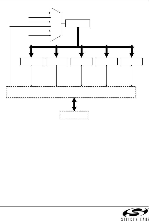
C8051F320/1 |
|
|
|
|
|
|
|
SYSCLK/12 |
|
|
|
|
|
|
SYSCLK/4 |
|
|
|
|
|
|
Timer 0 Overflow |
PCA |
16-Bit Counter/Timer |
|
|
|
|
|
|
|
|
||
|
ECI |
|
CLOCK |
|
|
|
|
|
|
|
|
||
|
|
MUX |
|
|
|
|
|
SYSCLK |
|
|
|
|
|
|
|
|
|
|
|
|
|
External Clock/8 |
|
|
|
|
|
|
Capture/Compare |
Capture/Compare |
Capture/Compare |
Capture/Compare |
Capture/Compare |
|
|
Module 0 |
|
Module 1 |
Module 2 |
Module 3 |
Module 4 / WDT |
ECI |
CEX0 |
|
CEX1 |
CEX2 |
CEX3 |
CEX4 |
|
|
|
Crossbar |
|
|
|
Port I/O
Figure 1.9. PCA Block Diagram
1.9.10-Bit Analog to Digital Converter
The C8051F320/1 devices include an on-chip 10-bit SAR ADC with a 17-channel differential input multiplexer. With a maximum throughput of 200 ksps, the ADC offers true 10-bit linearity with an INL of ±1LSB. The ADC system includes a configurable analog multiplexer that selects both positive and negative ADC inputs. Ports1-3 are available as ADC inputs; additionally, the on-chip Temperature Sensor output and the power supply voltage (VDD) are available as ADC inputs. User firmware may shut down the ADC to save power.
Conversions can be started in six ways: a software command, an overflow of Timer 0, 1, 2, or 3, or an external convert start signal. This flexibility allows the start of conversion to be triggered by software events, a periodic signal (timer overflows), or external HW signals. Conversion completions are indicated by a status bit and an interrupt (if enabled). The resulting 10-bit data word is latched into the ADC data SFRs upon completion of a conversion.
Window compare registers for the ADC data can be configured to interrupt the controller when ADC data is either within or outside of a specified range. The ADC can monitor a key voltage continuously in background mode, but not interrupt the controller unless the converted data is within/outside the specified range.
24 |
Rev. 1.2 |

C8051F320/1
Analog Multiplexer
|
P1.0 |
|
|
|
|
|
|
|
|
|
Configuration, Control, and Data Registers |
|
|
||
|
P1.7 |
|
|
|
|
|
|
|
P2.0 |
|
|
|
|
|
|
P2.4-2.7 |
|
19-to-1 |
|
|
|
000 |
AD0BUSY (W) |
|
AMUX |
|
|
Start |
|||
available on |
|
|
|
|
001 |
Timer 0 Overflow |
|
P2.7 |
|
|
|
Conversion |
|||
C8051F320 |
|
|
|
010 |
Timer 2 Overflow |
||
|
|
|
|
||||
|
P3.0 |
|
|
|
|
011 |
Timer 1 Overflow |
|
|
|
|
|
|
||
Temp |
|
|
|
|
|
100 |
CNVSTR Input |
|
|
|
|
|
101 |
Timer 3 Overflow |
|
Sensor |
VDD |
|
|
|
|
||
|
|
|
|
|
|
||
|
|
|
|
|
|
|
|
|
|
|
(+) |
10-Bit |
|
|
|
|
|
|
SAR |
|
|
|
|
|
|
|
|
|
|
ADC Data |
|
|
|
|
|
ADC |
16 |
|
Registers |
|
P1.0 |
|
(-) |
|
|
|
|
|
|
|
|
|
|
||
|
|
|
|
|
|
|
|
|
P1.7 |
|
|
|
|
|
Window |
|
P2.0 |
|
|
|
Window Compare |
||
|
19-to-1 |
|
|
Compare |
|||
|
|
|
End of |
|
Logic |
||
|
|
AMUX |
|
|
Interrupt |
||
P2.4-2.7 |
|
|
Conversion |
|
|
||
|
|
|
|
|
|
||
available on |
P2.7 |
|
|
Interrupt |
|
|
|
C8051F320 |
|
|
|
|
|
|
|
|
P3.0 |
|
|
|
|
|
|
|
VREF |
|
|
|
|
|
|
|
GND |
|
|
|
|
|
|
Figure 1.10. 10-Bit ADC Block Diagram
1.10. Comparators
C8051F320/1 devices include two on-chip voltage comparators that are enabled/disabled and configured via user software. Port I/O pins may be configured as comparator inputs via a selection mux. Two comparator outputs may be routed to a Port pin if desired: a latched output and/or an unlatched (asynchronous) output. Comparator response time is programmable, allowing the user to select between high-speed and low-power modes. Positive and negative hysteresis are also configurable.
Comparator interrupts may be generated on rising, falling, or both edges. When in IDLE mode, these interrupts may be used as a “wake-up” source. Comparator0 may also be configured as a reset source. Figure 1.11 shows the Comparator0 block diagram.
Rev. 1.2 |
25 |
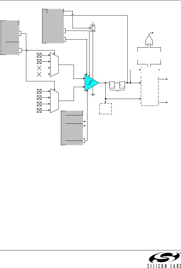
C8051F320/1
|
|
|
CP0EN |
|
|
|
|
|
CP0OUT |
|
|
CPT0MX |
|
CPT0CN |
CP0RIF |
VDD |
|
|
CP0FIF |
|
|
||
|
|
|
|
|
|
|
|
|
CP0HYP1 |
|
CP0 |
|
CMX0N1 |
|
CP0HYP0 |
|
|
|
|
|
|
Interrupt |
|
|
CMX0N0 |
|
CP0HYN1 |
|
|
|
|
|
|
||
|
|
|
|
|
|
|
|
|
CP0HYN0 |
|
|
|
CMX0P1 |
|
|
|
|
|
CMX0P0 |
P1.0 |
|
CP0 |
CP0 |
|
|
|
|||
|
|
|
Rising-edge |
Falling-edge |
|
|
|
|
|
||
|
|
P1.4 |
|
|
|
P2.0 |
|
|
CP0 + |
|
|
|
|
|
|
|
|
|
|
|
|
|
|
|
|
|
|
|
|
|
|
||
|
|
|
|
|
|
|
Interrupt |
|
|
|
|
CP0RIE |
|||||||||||||||
P2.4 |
|
|
|
|
|
|
|
|
|
|
Logic |
|
|
|
|
CP0FIE |
|||||||||||
|
|
|
|
|
|
|
|
|
|
|
|
||||||||||||||||
|
|
|
|
|
|
|
|
|
|
|
|
|
|
|
|
|
|
|
|
|
|
|
|
|
|
|
|
|
|
|
|
|
|
|
|
|
|
|
|
|
|
|
|
|
|
|
|
|
|
|
|
|
|
||
|
|
|
|
|
|
|
|
|
|
|
|
|
|
|
|
|
|
|
|
|
|
|
|
|
|
|
|
+ |
|
|
|
|
CP0 |
|
D SET |
Q |
D SET |
Q |
|
- |
CLR |
Q |
CLR |
Q |
|
P1.1 |
|
|
Crossbar |
|
|
|
(SYNCHRONIZER) |
P1.5 |
CP0 - |
GND |
|
|
CP0A |
||
|
|
|
|
P2.1 |
|
|
Reset |
|
|
|
|
P2.5 |
|
|
Decision |
|
|
Tree |
|
|
|
|
|
|
CPT0MD |
CP0RIE |
|
Note: P2.4 and P2.5 available |
CP0FIE |
|
|
|
|
||
only on C8051F320 |
|
|
|
|
|
CP0MD1 |
|
|
|
CP0MD0 |
|
Figure 1.11. Comparator0 Block Diagram
26 |
Rev. 1.2 |

C8051F320/1
2.Absolute Maximum Ratings
Table 2.1. Absolute Maximum Ratings
Parameter |
Conditions |
Min |
Typ |
Max |
Units |
|
|
|
|
|
|
Ambient temperature under bias |
|
–55 |
— |
125 |
°C |
|
|
|
|
|
|
Storage Temperature |
|
–65 |
— |
150 |
°C |
|
|
|
|
|
|
Voltage on any Port I/O Pin or /RST with |
|
–0.3 |
— |
5.8 |
V |
respect to GND |
|
|
|
|
|
|
|
|
|
|
|
Voltage on VDD with respect to GND |
|
–0.3 |
— |
4.2 |
V |
|
|
|
|
|
|
Maximum Total current through VDD and |
|
— |
— |
500 |
mA |
GND |
|
|
|
|
|
|
|
|
|
|
|
Maximum output current sunk by /RST or any |
|
— |
— |
100 |
mA |
Port pin |
|
|
|
|
|
|
|
|
|
|
|
Note: Stresses above those listed under “Absolute Maximum Ratings” may cause permanent damage to the device. This is a stress rating only and functional operation of the devices at those or any other conditions above those indicated in the operation listings of this specification is not implied. Exposure to maximum rating conditions for extended periods may affect device reliability.
Rev. 1.2 |
27 |

C8051F320/1
3.Global Electrical Characteristics
Table 3.1. Global Electrical Characteristics
–40 to +85 °C, 25 MHz system clock unless otherwise noted.
Parameter |
Conditions |
Min |
Typ |
Max |
Units |
|
|
|
|
|
|
Digital Supply Voltage |
|
1,2 |
3.0 |
3.6 |
V |
|
VRST |
||||
Digital Supply RAM Data |
|
- |
1.5 |
— |
V |
Retention Voltage |
|
|
|
|
|
|
|
|
|
|
|
SYSCLK (System Clock)3 |
|
0 |
— |
25 |
MHz |
TSYSH (SYSCLK High Time) |
|
18 |
— |
— |
ns |
TSYSL (SYSCLK Low Time) |
|
18 |
— |
— |
ns |
Specificed Operating Tem- |
|
–40 |
— |
+85 |
°C |
perature Range |
|
|
|
|
|
|
|
|
|
|
|
Digital Supply Current - CPU Active (Normal Mode, fetching instructions from Flash) |
|
||||
|
|
|
|
|
|
IDD4 |
VDD = 3.6 V; F = 25 MHz |
— |
12.3 |
13.6 |
mA |
|
VDD = 3.3 V, F = 24 MHz |
— |
10.6 |
11.5 |
mA |
|
VDD = 3.3 V, F = 6 MHz |
— |
3.2 |
— |
mA |
|
VDD = 3.3 V, F = 32 kHz |
— |
38 |
— |
uA |
|
VDD = 3.0 V, F = 24 MHz |
— |
9.0 |
9.8 |
mA |
|
VDD = 3.0 V, F = 6 MHz |
— |
2.7 |
— |
mA |
|
VDD = 3.0 V, F = 32 kHz |
— |
32 |
— |
uA |
IDD Supply Sensitivity4 |
F = 24 MHz |
— |
0.66 |
— |
%/V |
|
F = 6 MHz |
— |
0.63 |
— |
%/V |
|
|
|
|
|
|
IDD Frequency Sensitivity4,5 |
VDD = 3.0 V, F < 15 MHz, T = 25 °C |
— |
0.45 |
— |
mA/MHz |
|
VDD = 3.0 V, F > 15 MHz, T = 25 °C |
— |
0.26 |
— |
mA/MHz |
|
VDD = 3.3 V, F < 15 MHz, T = 25 °C |
— |
0.53 |
— |
mA/MHz |
|
VDD = 3.3 V, F > 15 MHz, T = 25 °C |
— |
0.29 |
— |
mA/MHz |
Digital Supply Current - CPU and USB Active (USB Transceiver Enabled and Connected to PC)
IDD4 |
VDD = 3.3 V, F = 24 MHz, Full Speed |
— |
16.8 |
— |
mA |
|
VDD = 3.0 V, F = 24 MHz, Full Speed |
— |
14.4 |
— |
mA |
|
VDD = 3.3 V, F = 6 MHz, Low Speed |
— |
7.2 |
— |
mA |
|
VDD = 3.0 V, F = 6 MHz, Low Speed |
— |
6.0 |
— |
mA |
Digital Supply Current - CPU Inactive (Idle Mode, not fetching instructions from Flash) |
|
||||
|
|
|
|
|
|
IDD4 |
VDD = 3.6 V; F = 25 Mhz |
— |
5.8 |
6.5 |
mA |
|
VDD = 3.3 V, F = 24 MHz |
— |
5.2 |
5.9 |
mA |
|
VDD = 3.3 V, F = 6 MHz |
— |
1.7 |
— |
mA |
|
VDD = 3.3 V, F = 32 kHz |
— |
14 |
— |
uA |
|
VDD = 3.0 V, F = 24 MHz |
— |
4.6 |
5.2 |
mA |
|
VDD = 3.0 V, F = 6 MHz |
— |
1.5 |
— |
mA |
|
VDD = 3.0 V, F = 32 kHz |
— |
11 |
— |
uA |
28 |
Rev. 1.2 |

C8051F320/1
Table 3.1. Global Electrical Characteristics (Continued)
–40 to +85 °C, 25 MHz system clock unless otherwise noted.
Parameter |
Conditions |
Min |
Typ |
Max |
Units |
|
|
|
|
|
|
IDD Supply Sensitivity4 |
F = 24 MHz |
— |
0.47 |
— |
%/V |
|
F = 6 MHz |
— |
0.50 |
— |
%/V |
|
|
|
|
|
|
IDD Frequency Sensitivity 4,6 |
VDD = 3.0 V, F < 1 MHz, T = 25 °C |
— |
0.25 |
— |
mA/MHz |
|
VDD = 3.0 V, F > 1 MHz, T = 25 °C |
— |
0.17 |
— |
mA/MHz |
|
VDD = 3.3 V, F < 1 MHz, T = 25 °C |
— |
0.29 |
— |
mA/MHz |
|
VDD = 3.3 V, F > 1 MHz, T = 25 °C |
— |
0.20 |
— |
mA/MHz |
Digital Supply Current |
Oscillator not running, |
— |
<0.1 |
— |
uA |
(Stop Mode) |
VDD Monitor disabled |
|
|
|
|
Notes:
1. Given in Table 10.1, “Reset Electrical Characteristics,” on page 104. 2. USB requires a minimum supply voltage of 3.0 V.
3. SYSCLK must be at least 32 kHz to enable debugging.
4. Based on device characterization data; Not production tested.
5. IDD can be estimated for frequencies < 15 MHz by simply multiplying the frequency of interest by the frequency sensitivity number for that range. When using these numbers to estimate IDD for >15 MHz, the estimate should be the current at 24 MHz minus the difference in current indicated by the frequency sensitivity number. For example: VDD = 3.0 V; F = 20 MHz, IDD = 9.0 mA – (24 MHz –
20 MHz) x 0.26 mA/MHz = 7.96 mA.
6. Idle IDD can be estimated for frequencies < 1 MHz by simply multiplying the frequency of interest by the frequency sensitivity number for that range. When using these numbers to estimate Idle IDD for >1 MHz, the estimate should be the current at 24 MHz minus the difference in current indicated by the frequency sensitivity number. For example: VDD = 3.0 V; F = 5 MHz, Idle IDD = 4.6 mA – (24 MHz –
5 MHz) x 0.17 mA/MHz = 1.37 mA.
Table 3.2. Index to Electrical Characteristics Tables
Peripheral Electrical Characteristics |
Page # |
|
|
ADC0 Electrical Characteristics |
53 |
|
|
Voltage Reference Electrical Characteristics |
55 |
|
|
Comparator Electrical Characteristics |
65 |
|
|
Voltage Regulator Electrical Characteristics |
67 |
|
|
Reset Electrical Characteristics |
104 |
|
|
Flash Electrical Characteristics |
106 |
|
|
Internal Oscillator Electrical Characteristics |
124 |
|
|
Port I/O DC Electrical Characteristics |
137 |
|
|
Rev. 1.2 |
29 |

C8051F320/1
4.Pinout and Package Definitions
Table 4.1. Pin Definitions for the C8051F320/1
Name |
Pin Numbers |
Type |
Description |
||
‘F320 |
‘F321 |
||||
|
|
|
|||
|
|
|
|
|
|
|
|
|
Power In |
2.7-3.6 V Power Supply Voltage Input. |
|
VDD |
6 |
6 |
Power |
|
|
|
|
|
|
||
|
|
|
Out |
3.3 V Voltage Regulator Output. See Section 8. |
|
|
|
|
|
|
|
GND |
3 |
3 |
|
Ground. |
|
|
|
|
|
|
|
/RST/ |
|
|
D I/O |
Device Reset. Open-drain output of internal POR or VDD |
|
|
|
|
|
monitor. An external source can initiate a system reset by |
|
|
9 |
9 |
|
driving this pin low for at least 15 µs. See Section 10. |
|
C2CK |
|
|
D I/O |
Clock signal for the C2 Debug Interface. |
|
|
|
|
|
|
|
P3.0/ |
|
|
D I/O |
Port 3.0. See Section 14 for a complete description. |
|
|
10 |
10 |
|
|
|
C2D |
|
|
D I/O |
Bi-directional data signal for the C2 Debug Interface. |
|
|
|
|
|
|
|
REGIN |
7 |
7 |
Power In |
5 V Regulator Input. This pin is the input to the on-chip volt- |
|
|
|
age regulator. |
|||
|
|
|
|
||
|
|
|
|
|
|
|
|
|
|
VBUS Sense Input. This pin should be connected to the |
|
VBUS |
8 |
8 |
D In |
VBUS signal of a USB network. A 5 V signal on this pin indi- |
|
|
|
|
|
cates a USB network connection. |
|
|
|
|
|
|
|
D+ |
4 |
4 |
D I/O |
USB D+. |
|
|
|
|
|
|
|
D- |
5 |
5 |
D I/O |
USB D–. |
|
|
|
|
|
|
|
P0.0 |
2 |
2 |
D I/O |
Port 0.0. See Section 14 for a complete description of Port 0. |
|
|
|
|
|
|
|
P0.1 |
1 |
1 |
D I/O |
Port 0.1. |
|
|
|
|
|
|
|
P0.2/ |
|
|
D I/O |
Port 0.2. |
|
|
32 |
28 |
|
External Clock Input. This pin is the external oscillator return |
|
|
|
|
|
||
XTAL1 |
|
|
A In |
for a crystal or resonator. See Section 13. |
|
|
|
|
|
|
|
P0.3/ |
|
|
D I/O |
Port 0.3. |
|
|
31 |
27 |
|
External Clock Output. This pin is the excitation driver for an |
|
|
A I/O or |
external crystal or resonator, or an external clock input for |
|||
|
|
|
|||
XTAL2 |
|
|
D In |
CMOS, capacitor, or RC oscillator configurations. See Sec- |
|
|
|
|
|
tion 13. |
|
|
|
|
|
|
|
P0.4 |
30 |
26 |
D I/O |
Port 0.4. |
|
|
|
|
|
|
|
P0.5 |
29 |
25 |
D I/O |
Port 0.5. |
|
|
|
|
|
|
|
P0.6/ |
|
|
|
Port 0.6. |
|
|
28 |
24 |
|
|
|
CNVSTR |
|
|
|
ADC0 External Convert Start Input. See Section 5. |
|
|
|
|
|
|
|
P0.7/ |
|
|
D I/O |
Port 0.7. |
|
|
27 |
23 |
|
|
|
VREF |
|
|
A I/O |
External VREF input or output. See Section 6. |
|
|
|
|
|
|
|
P1.0 |
26 |
22 |
D I/O or |
Port 1.0. See Section 14 for a complete description of Port 1. |
|
|
|
|
A In |
|
|
30 |
Rev. 1.2 |
Loading...