

Page 1
5-V Voltage Regulator TLE 4286 G
Features
• Wide operation range: 6.2 V to 42 V
• Wide temperature range: – 40 °C to 150 °C
• Low quiescent current consumption: 50 µA
• Output protected against short circuit
• Over-temperature protection
• Inhibit input
• Very low current consumption in
stand-by (Inhibit) mode
• Very small SMD-Package SCT-595
SCT-595
Type Ordering Code Package
TLE 4286 G Q67006-A9304 SCT-595 (SMD)
Functional Description
The TLE 4286 G is a 5-V low-drop fixed voltage regulator in the very small SMD package
SCT-595. The maximum input voltage is 42 V. The output is able to drive a load of more
than 10 mA while it regulates the output voltage within a 4% accuracy.
The device can be switched in stand-by mode via an inhibit input which causes the
current consumption to drop below 1 µA.
A temperature protection that disables the circuit at over temperature is incorporated.
Semiconductor Group 1 1998-11-01
Page 2
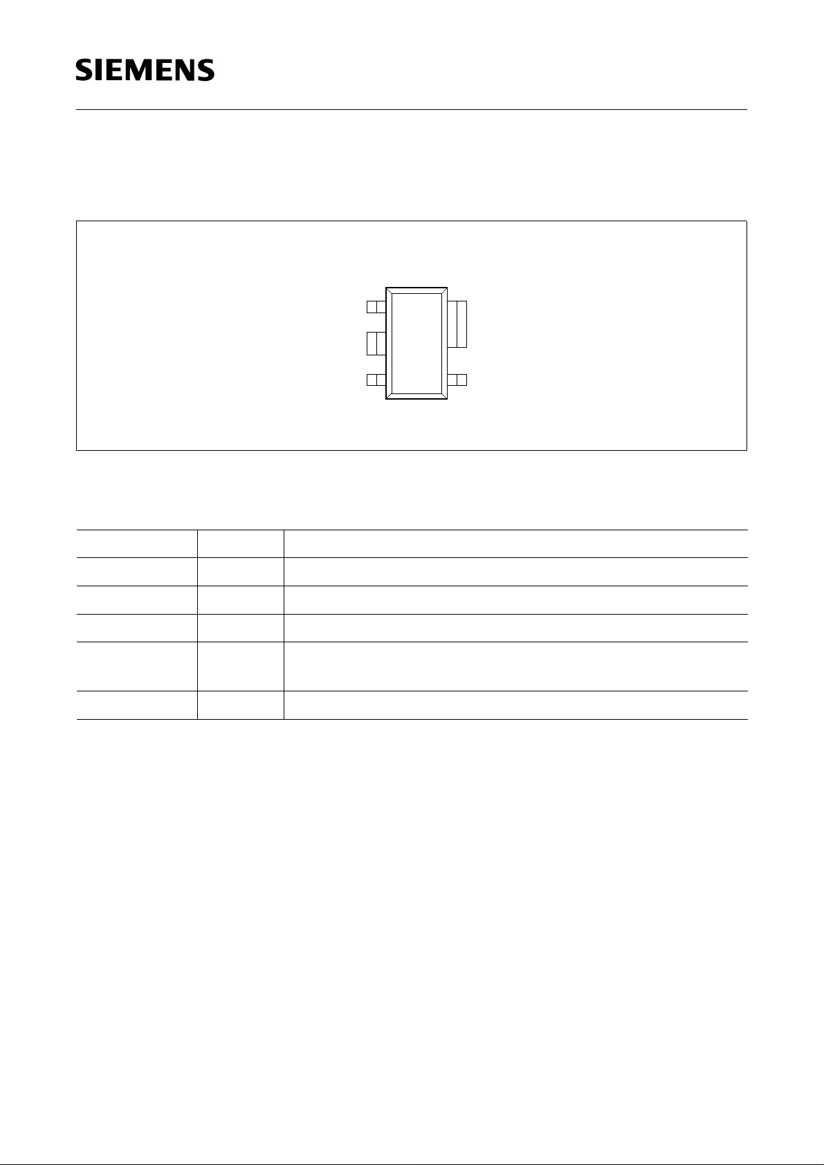
Pin Configuration
(top view)
TLE 4286 G
SCT-595
INH
GND
1
5
GND
2
4
AEP02253
Q
3
Ι
Figure 1
Pin Definitions and Functions
Pin No. Symbol Function
V
1INHInhibit input; H for active (
= 5 V) and L for stand-by
Q
2GNDGround; internally connected to pin 5
3IInput voltage
4QOutput voltage; must be blocked by a capacitor
C
≥ 1 µF, ESR ≤ 10 Ω to GND
Q
5GNDGround; internally connected to pin 2
Semiconductor Group 2 1998-11-01
Page 3
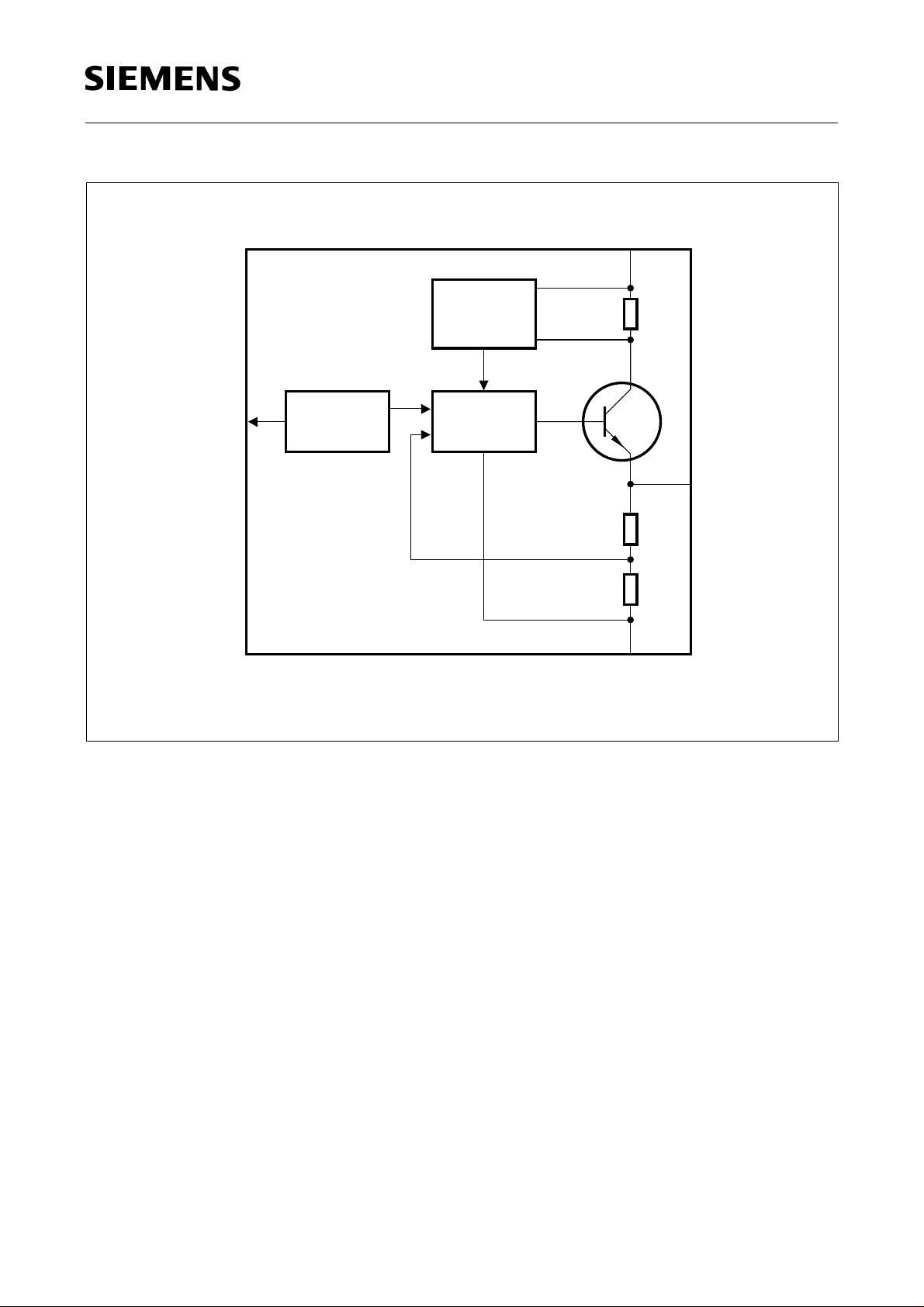
Protection
TLE 4286 G
Ι
3
Figure 2
Block Diagram
INH
1
Reference
Regulator
4
Q
2, 5
GND
AEB02189
Semiconductor Group 3 1998-11-01
Page 4

Absolute Maximum Ratings
TLE 4286 G
–40 °C <
T
< 150 °C
j
Parameter Symbol Limit Values Unit Remarks
min. max.
Input
Voltage
Current
V
I
I
I
– 0.3 45 V –
– 20 * mA * internally limited
Output
Voltage
Current
V
I
Q
Q
– 0.3 16 V –
– 20 * mA * internally limited
Inhibit
Voltage
Current
V
I
INH
INH
– 40 45 V –
– 500 * µA * internally limited
Current
I
INH
– 5 5 mA – 0.3 V < VI < 45 V;
t
< 1 ms
p
Temperatures
Junction temperature
Storage temperature
T
j
T
stg
– 40 150 °C–
– 50 150 °C–
Thermal Resistances
Junction pin
Junction ambient
R
R
thj-pin
thja
– 30 K/W measured to pin 5
–55K/W
1)
Note: Maximum ratings are abs olute ratings; exceeding any one of th ese values may
cause irreversible damage to the integrated circuit.
1)
Package mounted on PCB 40 mm × 40 mm × 1.5 mm / 6 cm2 Cu (thickness Cu = 35 µm)
Semiconductor Group 4 1998-11-01
Page 5

TLE 4286 G
Operating Range
Parameter Symbol Limit Values Unit Remarks
min. max.
Input voltage
Logic input voltage (INH)
Junction temperature
V
V
T
I
INH
j
6.0 42 V –
– 0.3 40 V –
– 40 150 °C–
Semiconductor Group 5 1998-11-01
Page 6

TLE 4286 G
Electrical Characteristics
V
6.2 V <
< 36 V; V
I
Parameter Symbol Limit Values Unit Test Condition
Output
INH
> V
; – 40 °C < Tj < 150 °C; unless otherwise specified
INH, ON
min. typ. max.
Output voltage
Output voltage
Drop voltage
Output capacitor
Output current
Current Consumption
Quiescent current
Quiescent current
(stand-by)
Quiescent current
(stand-by)
V
V
V
C
I
I
I
I
Q
Q
dr
Q
4.85 5.0 5.15 V Tj = 25 °C;
I
1mA <
< 10 mA
Q
4.8 5.0 5.20 V 1 mA < IQ < 10 mA
0.6 0.8 1.1 V IQ = 10 mA
1––µFESR ≤ 10 Ω
at 10 kHz
Q
q
q
q
10 – 40 mA –
– 60 100 µA IQ < 10 mA;
V
= 13.5 V
I
––1µA V
––5µA V
< V
INH
T
< 85 °C
j
< V
INH
INH, OFF
INH, OFF
;
Regulator Performance
Load regulation ∆
Line regulation ∆
Power supply ripple
V
Q
V
Q
PSRR
rejection
Semiconductor Group 6 1998-11-01
– 5 10 mV 0 mA < IQ <10 mA;
V
= 6.2 V;
I
T
≤ 85 °C
j
–510mVIQ = 5 mA;
T
≤ 85 °C
j
–60–dBfr = 100 Hz;
V
= 0.5 V
r
SS
Page 7

Electrical Characteristics (cont’d)
TLE 4286 G
6.2 V <
V
< 36 V; V
I
INH
> V
; – 40 °C < Tj < 150 °C; unless otherwise specif ied
INH, ON
Parameter Symbol Limit Values Unit Test Condition
min. typ. max.
Logic Inhibit Input
Inhibit ON-threshold
Inhibit OFF-threshold
H-input current
L-input c urrent
6.2 ... 36V
Inhibit
V
INH, ON
V
INH, OFF
I
INH, ON
I
INH, OFF
C
Ι
100
––3.5VVQ ≥ 4.8 V
0.3 – – V VQ ≤ 0.8 V
–1015µA V
– 2 0 2 µA V
5V
C
Q
µ1 F
nF
V
Ι
34
TLE 4286G
INH
1
2, 5
GND
V
Q
INH
INH
= 5 V
= 0 V
Figure 3
Application Circuit
AES02190
Semiconductor Group 7 1998-11-01
Page 8

TLE 4286 G
V
Output Voltage VQ versus
= 1 mA
Q
j
Ι
= 10 mA
Q
40
80 120 160
Temperature T
5.10
V
V
Q
5.05
5.00
4.95
4.90
4.85
4.80
Ι
-40 0
AED02191
C
T
j
Output Voltage V
Output Current I
6
V
Q
T
= 130 C 25 C -40 C
j
5
4
3
2
1
0
0
versus
Q
Q
2010
AED02192
30
mA
Ι
Q
40
T
j
-40 C
25 C
130 C
2.5
versus
dr
Q
=
Inhibit Voltage V
Inhibit Current I
AED02193
7.55
10
mA
Ι
Q
15
Ι
INH
120
µ
A
100
T
j
80
60
40
20
0
010
= 130 C
Drop Voltage V
Output Current I
1200
mV
V
dr
1000
800
600
400
200
0
0
INH
INH
25 C
-40 C
20
versus
30
AED02194
40 50
V
V
INH
Semiconductor Group 8 1998-11-01
Page 9

Package Outlines
SCT-595
(Plastic Dual Small Outline)
B
+0.1
1.2
-0.05
A
+0.1
0.6
-0.05
2.9
(2.2)
±0.2
(0.3)
0.3
0.95
+0.2
acc. to
DIN 6784
+0.1
-0.05
0.25 min
2.6 max
0.20
1.1 max
10˚max
0.15
M
A
0.1 max
+0.1
-0.06
TLE 4286 G
±0.1
1.6
10˚max
1.9
0.25MB
GPW05997
Sorts of Packing
Package outlines for tubes, trays etc. are contained in our
Data Book “Package Information”.
SMD = Surface Mounted Device
Dimensions in mm
Semiconductor Group 9 1998-11-01
 Loading...