

Page 1
现货库存、技术资料、百科信息、热点资讯,精彩尽在鼎好!
5-V Low-Drop Voltage Regulator TLE 4263
Features
● Output voltage tolerance ≤ ± 2 %
● Low-drop voltage
● Very low standby current consumption
● Overtemperature protection
● Reverse polarity protection
● Short-circuit proof
● Settable reset threshold
● Watchdog
● Wide temperature range
● Suitable for use in automotive electronics
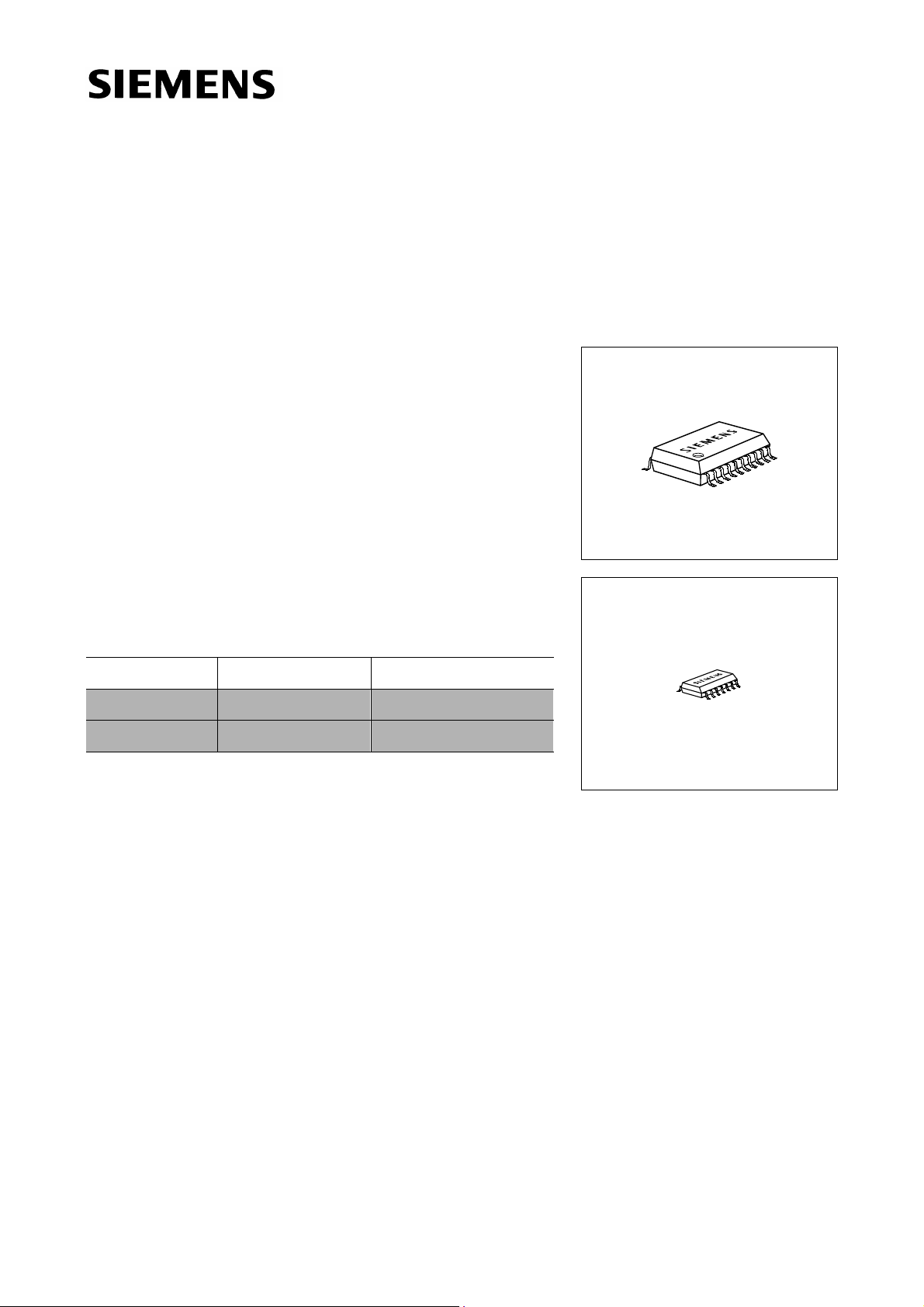
P-DSO-20-6
Type Ordering Code Package
TLE 4263 G Q67006-A9095 P-DSO-20-6 (SMD)
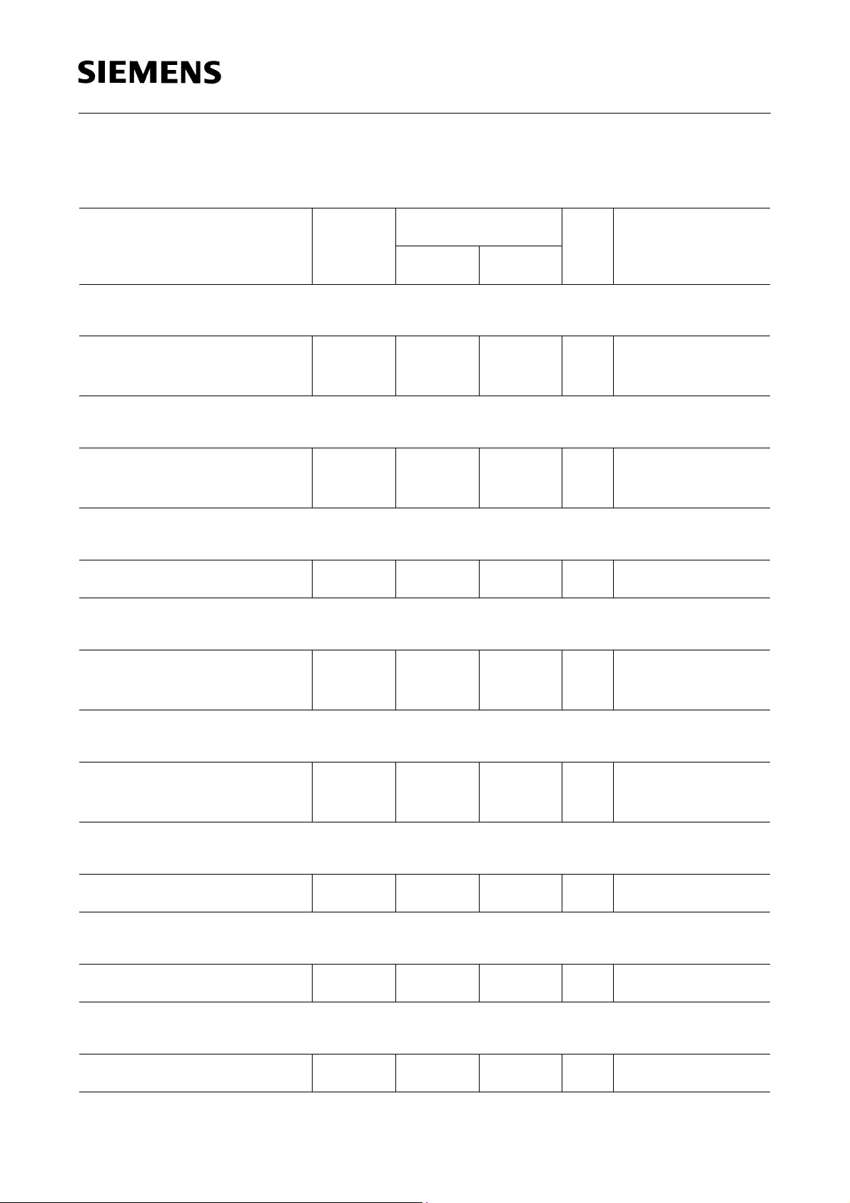
TLE 4263 GM Q67006-A9357 P-DSO-14-4 (SMD)
▼
New type
▼
P-DSO-14-4
Functional Description
TLE 4263 G is a 5-V lo w-drop voltage regulator i n a P-DSO-20-6 SMD package. The
maximum input voltage is 45 V. The maximum output current is more than 200 mA. The
IC is short-circuit proof and incorporates tempe rature protection that disabl es the IC at
overtemperature.
V
The IC regulates an inp ut v oltage
in the range of 6 V < VI < 45 V to V
I
reset signal is generated for an output voltage of
V
< 4.5 V. This voltage threshold can
Q
= 5.0 V. A
Qrated
be decreased to 3.5 V by external connection . The res et de lay can be set exte rnall y by
a capacitor. The integrated watchdo g logic co ntrol s the connecte d micr ocontrol ler. The
IC can be switched off via the inhibit input, which causes the current consumption to drop
from 800 µA to < 50 µA.
Semiconductor Group 1 1998-11-01
Page 2

TLE 4263
Dimensioning Information on External Components
C
The input capacitor
approx. 1 Ω in series with
capacitance can be dampe d. The output capacitor is necessary for the stability of the
regulating circuit. Stability is guaranteed at values ≥ 22 µF and an ESR of ≤ 3 Ω within
the operating temperature range. For small tole rances of the reset delay the spread of
the capacitance of the delay capacitor and its temperature coefficient should be noted.
Pin Configuration
(top view)
is necessary for compensating line influences. Using a resistor of
I
C
, the oscillating circuit consisting of input inductivity and input
I
TLE 4263 G
TLE 4263 GM
N.C.
QRES
GND
GND
GND
DRES
SRES
1
2
3
4
5
6
7
14
13
12
11
10
9
8
AEP02587
INH
V
Ι
GND
GND
GND
V
Q
W
Semiconductor Group 2 1998-11-01
Page 3

TLE 4263
Pin Definitions and Functions
Pin Symbol Function
1, 2, 19, 13 N.C. Not connected
3QRESReset output; open-collector output connected to the
output via a resistor of 30 kΩ.
4-7,
GND Ground
14-17
9 DRES Reset delay; connected to ground with a capacitor.
10 SRES Reset threshold; for setting the switching threshold
connect with a voltage divider from output to ground. If this
input is connected to GND, reset is triggered at an output
voltage of 4.5 V.
11 W Watchdog; positive edge triggered input for monitoring a
microcontroller.
12
V
Q
5-V output voltage; block to ground with a 22−µF
capacitor.
18
V
I
Input voltage; block to ground directly at the IC with a
ceramic capacitor.
20 INH Inhibit; TTL-compatible, low-active input.
Semiconductor Group 3 1998-11-01
Page 4

TLE 4263
Circuit Description
The control amplifie r compares a reference voltage, which i s kept highly accurate by
resistance adjustment, to a voltag e t hat is proporti onal to the o utput v oltage and d rives
the base of the series transistor via a buffer. Saturation control as a function of the load
current prevents any over-saturation of the power element. If the externally scaled down
output voltage at the reset threshold inpu t drops below 1.35 V, the external reset delay
capacitor is discharged by the reset gen erator. If the voltage on the capacito r reaches
V
the lower threshold
again until the upper threshold
to GND, reset is trigge red at an out put voltage of 4.5 V. A connected microcontrol ler is
controlled by the watchdog logic. If pulses are missing, the reset output is set to low. The
pulse sequence time can be set within a wide range with the reset delay capa cito r. The
IC can be switched at the TTL-compatible, low-active inhibit input. The IC also
incorporates a number of internal circuits for protection against:
, a reset signal i s issued on the rese t output and not canc elled
ST
V
is exceeded. If the reset threshold input is connected
dT
● Overload
● Overtemperature
● Reverse polarity
18
Input
Adjustment
Temperature
Sensor
Bandgap
Reference
Control
Amplifier
Saturation
Control and
Protection
Circuit
Buffer
11
Watchdog
Reset
Generator
12
Output
9
Reset
Delay
3
Reset
Output
10
Reset
Threshold
20
Inhibit
4-7, 14-17
GND
AEB01100
Block Diagram
Semiconductor Group 4 1998-11-01
Page 5
TLE 4263
Absolute Maximum Ratings
T
= – 40 to 150 °C
j
Parameter Symbol Limit Values Unit Remarks
min. max.
Input
Input voltage
Input current
Reset Output
Voltage
Current
Reset Input
Reset threshold
Reset Delay
Voltage
Current
Output
V
I
V
I
V
V
I
I
I
R
R
RE
d
d
–42
–
– 0.3
–
– 0.3 6 V –
–0.3
–
45
–
42
–
42
–
V
–
V
–
V
–
–
internally limited
–
internally limited
–
internally limited
Voltage
Current
V
I
Q
Q
–0.3
–
7
–
V
–
–
internally limited
Inhibit
Voltage
V
e
–42 45 V –
Watchdog
Voltage
V
W
–0.3 6 V –
Ground
Current
Semiconductor Group 5 1998-11-01
I
GND
–0.5 – A –
Page 6

TLE 4263
Absolute Maximum Ratings (con t’d)
T
= – 40 to 150 °C
j
Parameter Symbol Limit Values Unit Remarks
min. max.
Temperature
Junction temperature
Storage temperature
Operating Range
Input voltage
Junction temperature
Thermal resistance
junction-ambient
junction-case
T
T
V
T
R
R
j
stg
I
j
th JA
th JC
–
–50
150
150
°C
°C
–
–
–45V–
– 40 150 °C–
–
–
70
25
K/W
K/W
soldered
–
Semiconductor Group 6 1998-11-01
Page 7

TLE 4263
Characteristics
V
= 13.5 V; Tj = 25 °C; Ve > 3.5 V; (unless specified otherwise)
I
Parameter Symbol Limit Values Unit Test Condition
min. typ. max.
Normal Operation
Output voltage
Output voltage
Output current
Current consumption;
I
= Ii – I
q
Q
Drop voltage
V
V
I
I
I
I
I
V
Q
q
q
q
q
Load regulation ∆V
Supply-voltage
∆
regulation
Q
Q
Dr
V
4.90 5.00 5.10 V 5 mA ≤ IQ ≤ 150 mA;
V
6 V ≤
– 40 °C ≤
≤ 28 V;
I
T
≤ 125 °C
j
4.95 5.00 5.05 V 6 V ≤ VI ≤ 32 V;
I
= 100 mA;
Q
T
= 100 °C
j
200 250 – mA –
–
–
–
–
– 0.35 0.6 V IQ = 150 mA
Q
Q
––25mVIQ = 5 mA to 150 mA
–1525mVVI = 6 V to 28 V;
–
800
10
15
50
1100
15
20
µA
µA
mA
mA
V
= 0
e
I
= 0 mA
Q
I
= 150 mA
Q
I
= 150 mA; Vi = 4.5 V
Q
*)
I
= 150 mA
Q
Ripple rejection
SVR
–54–dBfr = 100 Hz; Vr = 0.5 Vpp
Reset Generator
Switching threshold
Switching voltage
Reset low voltage
Note: The reset output is low within the range VQ = 1 V to V
*)
Drop voltage = Vi – VQ (measured when the outp ut voltage has dropped 100 mV
from the nominal value obtained at 13.5 V input)
Semiconductor Group 7 1998-11-01
V
V
V
RT
RE
R
4.2 4.5 4.8 V VRE = 0 V
1.28 1.35 1.42 V VQ > 3.5 V
– 0.10 0.40 V IR = 1 mA
RT
Page 8

TLE 4263
Characteristics (cont’d)
V
= 13.5 V; Tj = 25 °C; Ve > 3.5 V; (unless specified otherwise)
I
Parameter Symbol Limit Values Unit Test Condition
min. typ. max.
Saturation voltage V
Delay switching
threshold
Switching threshold
Charge current
Delay time
Delay time
Watchdog
Discharge current
Switching voltage
Pulse time
V
V
I
t
t
I
V
T
d
d
t
Cd
C
dT
ST
Cd
W
–50100mVVQ < V
RT
1.5 1.7 2.1 V –
0.2 0.350.55V –
40 60 80 µA–
–2.8–msCd = 100 nF
–2–µs Cd = 100 nF
4.4 6.25 8.2 µA VC = 1.5 V
1.5 1.7 2.1 V –
–22.5–msCd = 100 nF
Inhibit
Switching voltage
Turn-OFF voltage
Input current
Note: The reset output is low within the range VQ = 1 V to V
Semiconductor Group 8 1998-11-01
V
V
I
e
e ON
e OFF
3.5 – – V IC turned on
– – 0.8 V IC turned off
51015µA Ve = 5 V
RT
Page 9

TLE 4263
Input
6 V ... 45 V
KL 15
Reset
to MC
Application Circuit
12
9
10
22 F
µ
100 nF
100 k
56 k
Output
Ω
Ω
470 nF
18
20
TLE 4263G
3
4
11
Watchdog
from MC
Ι
Ι
18
12
Ι
Q
AES01102
1000 F
VV
Ι+r
µ
470 nF
TLE 4263G
Ι
e
20
9
Ι
V
V
C
e
C
4
11
Ι
d
d
GND
V
W
10
V
9
RE
Ι
R
µ
22 F
5.6 k
Ω
V
Q
V
R
100 nF
VV
Dr
SVR = 20 log
*) Outside Control Range
V
-
=
*)
Ι
Q
V
r
V
∆
Q
AES01101
Test Circuit
Semiconductor Group 9 1998-11-01
Page 10

TLE 4263
V
Ι
t
<
t
V
RT
V
Q
d
Ι
V
d
=
d
t
C
V
dT
V
cd
V
ST
t
d
t
t
d
V
R
Over-
temperature
Voltage Drop
at Input
UndervoltagePower-on-Reset
Secondary
Spike
Time Response, Watchdog with High-Frequency Clock
Load
Bounce
AET01085
Semiconductor Group 10 1998-11-01
Page 11

TLE 4263
Reset Threshold versus
Output Voltage
1.6
V
V
RE
1.4
1.2
1.0
= 13.5 V
V
Ι
0.8
0.6
0.4
0.2
0
0
1
2
3
AED01098
5
4
V
V
Q
Switching Voltage
V
versus Temperature
ST
3.2
V
V
2.8
2.4
2.0
1.6
1.2
0.8
0.4
0
0-40
V
, VdT and
Cd
V
= 13.5 V
Ι
VV
,
dT
cd
V
ST
40
AED01087
12080
160
C
T
j
Reset Switching Threshold
versus Temperature
1.6
V
V
RE
1.4
1.2
1.0
0.8
0.6
0.4
0.2
0
-40
40
0 160
80 120
AED01088
C
T
j
Current Consumption of Inhibit
versus Temperature
12
µ
A
Ι
e
10
8
V
e
6
4
2
0
-40 0 8040 120
= 5 V
AED01089
C
T
j
160
Semiconductor Group 11 1998-11-01
Page 12

TLE 4263
Drop Voltage versus
OutputCurrent
800
mV
V
Dr
700
600
500
T
= 125 C
400
300
200
100
0
j
25 C
500 100
200150
AED01094
300
mA
Ι
Q
Current Consumption versus
Output Current
200
AED01095
mA
Ι
32
mA
Ι
q
28
24
20
V
= 13.5 V
Ι
16
12
8
4
0
100050
150
300
Q
Current Consumption versus
Input Voltage
30
mA
Ι
q
25
20
R
15
10
5
0
L
20010
= 25
Ω
30
AED01096
40
V
Output Voltage versus
Input Voltage
12
V
V
Q
10
8
6
R
= 25
L
4
2
50
V
Ι
0
0
4
2
AED01097
Ω
68
10
V
V
Ι
Semiconductor Group 12 1998-11-01
Page 13

TLE 4263
Charge Current and Discharge
Current versus Temperature
80
A
µ
Ι
70
Ι
d
60
= 13.5 V
V
50
Ι
V
C
= 1.5 V
40
30
20
10
Ι
Cd
0
0-40 40
AED01104
12080 160
T
j
C
Output Voltage versus
Temperat ure
5.2
V
V
Q
5.1
5.0
V
e
4.9
4.8
4.7
4.6
0-40
40
= 13.5 V
12080
AED01090
160
C
T
j
Pulse Time versus
Temperat ure
40
ms
T
W
35
30
25
20
15
10
5
0
0-40 40
V
= 13.5 V
Ι
C
= 100 nF
d
AED01106
12080 160
C
T
j
Input Response
2
V
∆
V
Ι
1
0
40
mV
V
∆
Q
20
0
-20
-40
-10
t
=
r
C
_
~
t
µ
1 s
f
= 22 F
Q
20100
µ
30
AED01092
50
40
s
µ
t
Semiconductor Group 13 1998-11-01
Page 14

TLE 4263
Output Current versus
Input Voltage
300
mA
T
Ι
Q
250
200
150
100
50
= 25 C
j
0
100
20
30
AED01091
40
50
V
V
Ι
Load Response
295
mA
Ι
∆
Q
150
5
200
mV
∆
V
Q
100
0
-100
-200
010-10
C
= 22 F
Q
20
µ
30
AED01093
40
50
µ
s
t
Semiconductor Group 14 1998-11-01
Page 15

Package Outlines
P-DSO-20-6
(Plastic Dual Small Outline)
1.27
+0.15
0.35
2)
0.2 24x
1120
-0.1
0.2
-0.2
2.45
0.1
7.6
2.65 max
10.3
0.35 x 45˚
1)
-0.2
+0.8
0.4
±0.3
+0.09
0.23
TLE 4263
8˚ max
Weight approx. 0.6 g
GPS05094
110
12.8
-0.2
1)
Index Marking
1) Does not include plastic or metal protrusions of 0.15 max per side
2) Does not include dambar protrusion of 0.05 max per side
Sorts of Packing
Package outlines for tubes, trays etc. are contained in our
Data Book “Package Information”.
SMD = Surface Mounted Device
Semiconductor Group 15 1998-11-01
Dimensions in mm
Page 16

P-DSO-14-1
(Plastic Dual Small Outline)
-0.1
0.2
-0.2
1.45
4
-0.2
1.75 max
TLE 4263
0.35 x 45˚
1)
+0.06
0.19
0.35
1.27
+0.15
2)
0.1
0.2 14x
±0.2
6
0.4
+0.8
8˚ max.
14 8
17
8.75
-0.2
1)
Index Marking
1) Does not include plastic or metal protrusion of 0.15 max. per side
2) Does not include dambar protrusion of 0.05 max. per side
GPS05093
Sorts of Packing
Package outlines for tubes, trays etc. are contained in our
Data Book “Package Information”.
SMD = Surface Mounted Device
Semiconductor Group 16 1998-11-01
Dimensions in mm
 Loading...