

5-V Low-Drop Voltage Regulator TLE 4261-2
Features
• High accuracy 5 V ± 2%
• Very low-drop voltage
• Very low quiescent current
• Low starting-current consumption
• Proof against reverse polarity
• Input voltage up to 42 V
• Overvoltage protection up to 65 V (
≤ 400 ms)
• Short-circuit-proof
• External setting of reset delay
• Integrated watchdog circuit
• Wide temperature range
• Overtemperature protection
• Suitable for automotive use
• EMC proofed (100 V/m)
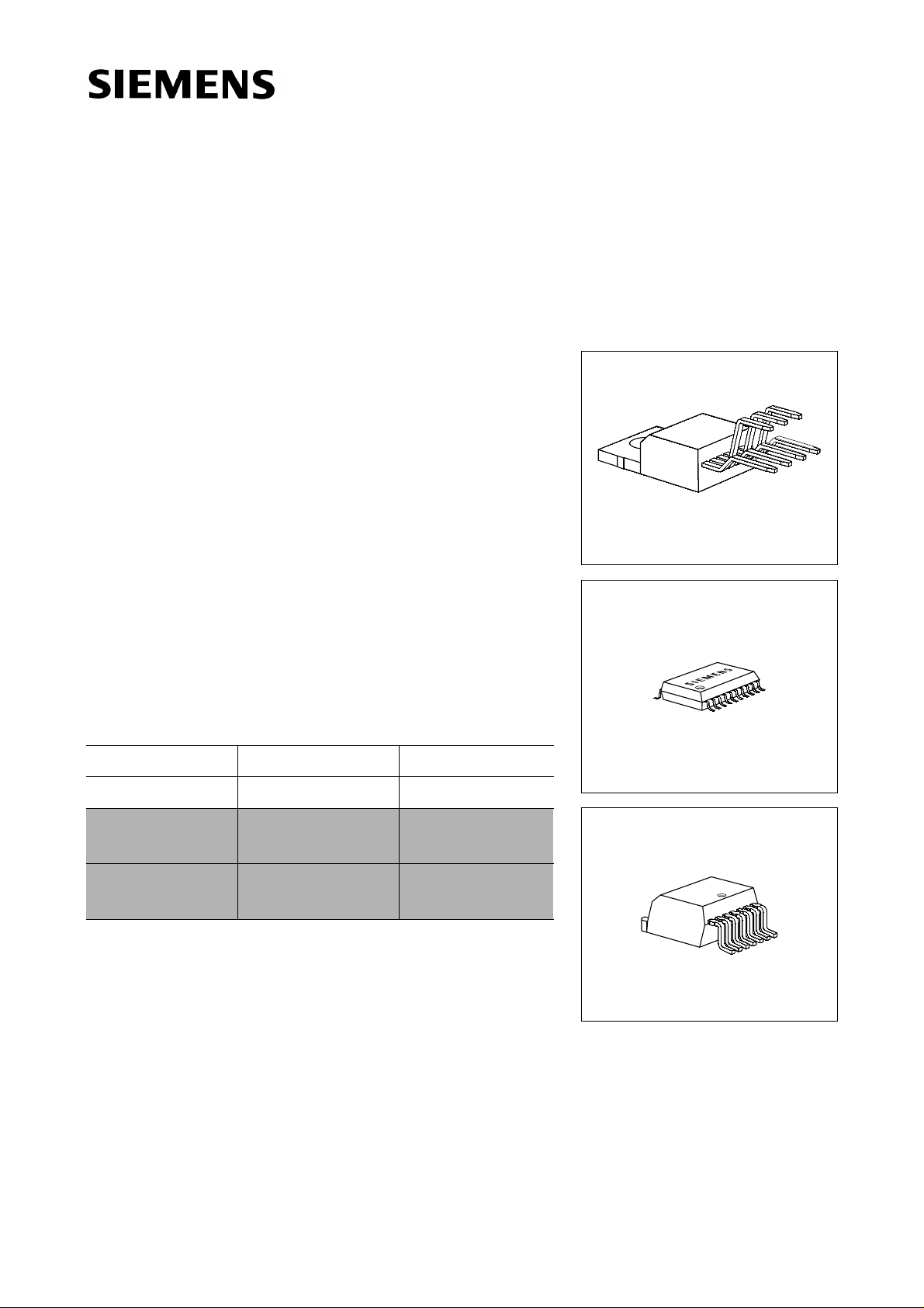
Type Ordering Code Package
▼ TLE 4261-2 Q67000-A9110 P-TO220-7-1
P-TO220-7-1
P-DSO-20-6
TLE 4261-2 G Q67000-A9140 P-DSO-20-6
▼
(SMD)
TLE 4261-2 GL Q67006-A9193 P-TO220-7-8
▼
(SMD)
▼ Please also refer to the new pin compatible device
TLE 4271
P-TO220-7-8
Functional Description
TLE 4261-2 is a high accuracy 5-V low-drop voltage regulator in a P-TO220-7 or in a PDSO package. The maximum input voltage is 42 V (65 V/≤ 400 ms). The device can
produce an output current of more than 500 mA. It is short-circuit-proof and incorporates
temperature protection that disables the circuit at impermissibly high temperatures.
Semiconductor Group 1 1998-11-01

TLE 4261-2
Application Description
V
The IC regulates an input voltage
reset signal is genera ted for an outpu t voltage
in the range 6V<V
I
V
of < 4.75 V. The reset delay c an be
O
set with an external capacitor. A connected microprocessor is monitored by the
integrated watchdog circui t; if pulses are missing, the reset ou tpu t is set low. The pulse
repetition rate can be set within wide limits with the capacitor for reset delay. If this input
is connected to a voltage of > 6 V, the watchdog function is deactivated. The device also
features an inhibit input, which is activated by a voltage of > 6 V
input through internal hysteresis up to approx. 3 V. A voltage of < 2 V on the inhibit input
turns off the regulator, current drain then dropping to max. 50
Design Notes for External Components
C
The input capacitor
causes a low-resistant p owerline and limi ts the rise t imes of the
I
input voltage. The IC is protected against rise times up to 100 V/
the tuned circuit consisting of supply inductance and input capacitance with a resistor of
approx. 1
Ω in series to C
.
I
The output capacitor maintains the stability of the regulating loop. Stability is guaranteed
with a rating of 22
µF min. at an ESR of 3 Ω max. in the operating temperature range.
<40V to V
I
Qrated
=5.0V. A
and then works on this
µA.
µs. It is possible to damp
Circuit Description
The control amplifier compares a reference voltage, which is kept highly accurate by
resistance adjustment, to a voltage that is proportional to the output voltage and controls
the base of the series PNP transistor via a buffer. Saturation control as a function of the
load current prevents any over-saturation of the power element. If the output voltage
drops below 95.5% of its typical value for more than 2
µs, a reset signal is triggered on
pin 3 and an e xternal capacitor discharged on pin 5. The reset signal is not cancelled
V
until the voltage on the ca pacitor has exceeded the upper switching thres hold
DT
. A
positive-edge-triggered watchdog circuit monitors the connected microprocessor and
will likewise trigger a reset if puls es are missing . The IC can be disa bled by a low le vel
on the inhibit input and the current consumption drops to
< 50 µA.
The IC also incorporates a number of circuits for protection against:
• Overload
• Overvoltage
• Overtemperature
• Reverse polarity
Semiconductor Group 2 1998-11-01
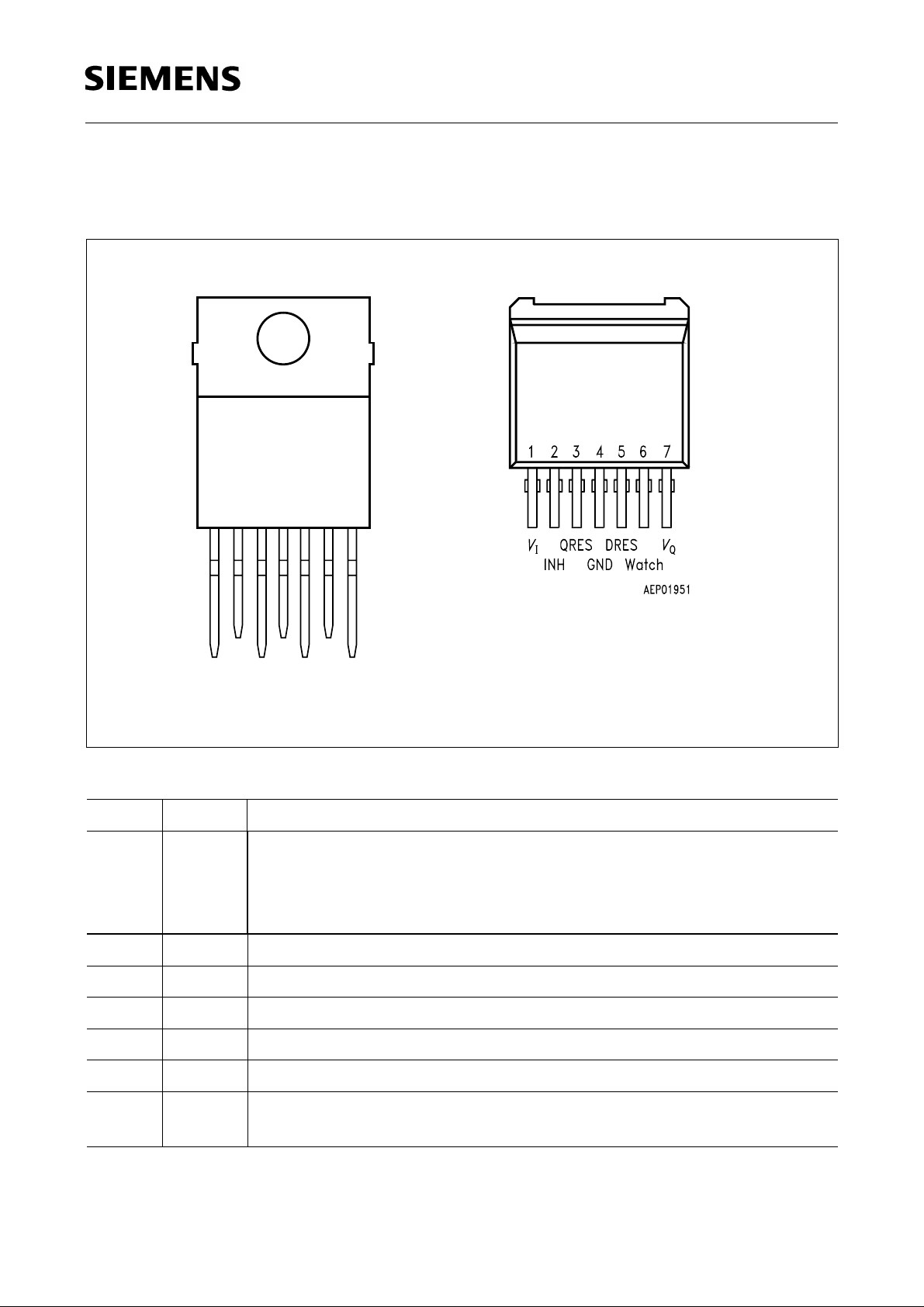
Pin Configuration
(top view)
TLE 4261-2 TLE 4261-2 GL
TLE 4261-2
4321567
INH
GND
Watch
V
QRES
Ι
DRES
V
Q
AEP00592
Pin Definitions and Functions
Pin No. Symbol Function
1
V
I
Input voltage; block a capacitor directly to ground on the IC. The
capacitor rating will depend on the vihicle electric system.
Oscillation of the output voltage can be damped by a resistor of
approx. 1 Ω in series with the input capacitor.
2INHInhibit; switches off the IC when low.
3QRESReset output; open collector output controlled by the reset delay.
4GNDGround
5 DRES Reset delay; wired to ground using a capacitor.
6WatchWatchdog; monitors the microprocessor when active.
7
V
Q
5-V output; block to ground using a capacitor of ≥ 22-µF. ESR is
≤ 3 Ω in the operating temperature range.
Semiconductor Group 3 1998-11-01
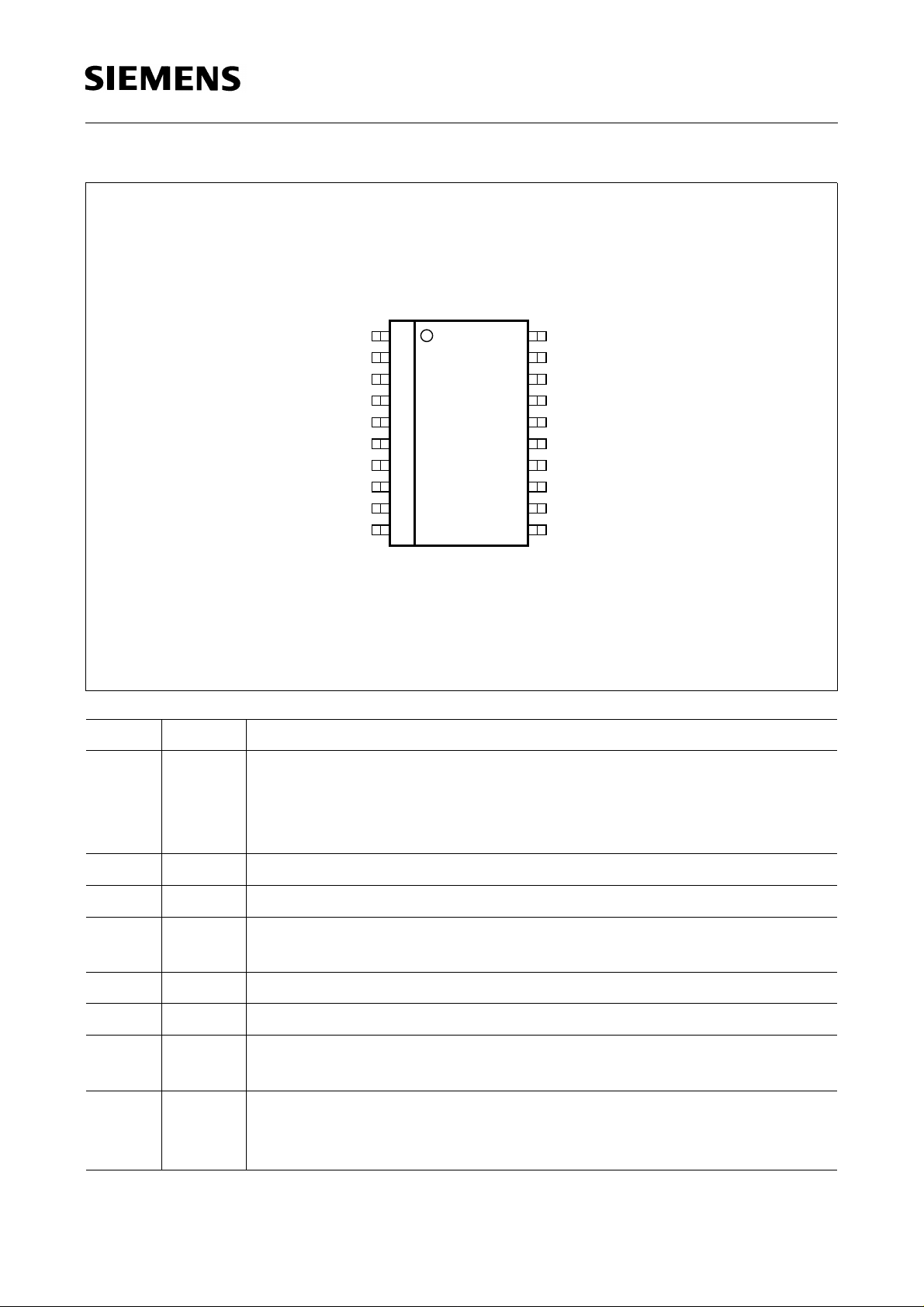
TLE 4261-2 G
TLE 4261-2
Pin No. Symbol Function
18
V
I
Input voltage; block a capacitor directly to ground on the IC. The
capacitor rating will depend on the vihicle electric system.
Oscillation of the output voltage can be damped by a resistor of
approx. 1 Ω in series with the input capacitor.
N.C.
N.C.
QRES
GND
GND 5
GND
N.C.
DRES
N.C.
1
2
3
4
6
7
8
9
10
20
19
18
17
16
15
14
13
12
11
AEP01182
INH
N.C.
V
Ι
GND
GND
GNDGND
GND
N.C.
V
Q
Watch
20 INH Inhibit; switches off the IC when low.
3QRESReset output; open collector output controlled by the reset delay.
4 -7,
GND Ground
14 - 17
9DRESReset delay; wired to ground using a capacitor.
11 Watch Watchdog; monitors the microprocessor when active.
12
V
Q
5-V output; block to ground using a capacitor of ≥ 22-µF. ESR is
≤ 3 Ω in the operating temperature range.
1, 2, 8,
N.C. Not connected
10, 13,
19
Semiconductor Group 4 1998-11-01
TLE 4261-2
Input
1
(18)
Overvoltage
Monitoring
Adjustment
Temperature
Sensor
Saturation
Control and
Protection
Control
Amplifier
BANDGAP
Reference
Inhibit
Buffer
+
-
RESET
Generator
Watchdog
(4-7)
2(20)
(11) 64(14-17)
Inhibit GND Watchdog
7
(12)
5
(9)
3
(3)
AEB00002
Output
RESET
Delay
RESET
Output
Block Diagram
Semiconductor Group 5 1998-11-01
TLE 4261-2
Absolute Maximum Ratings
T
= – 40 to 150 °C
J
Parameter Symbol Limit Values Unit Remarks
min. max.
Input
Input voltage
Input current
Inhibit
Voltage
Current
Reset Output
Voltage
Current
Ground
Current
V
V
I
I
V
I
2
V
I
R
I
GND
I
I
– 42 42 V –
–65 Vt ≤ 400 ms
–1.6 A–
2
– 0.3 42 V –
–5 mA–
R
– 0.3 42 V –
– – – internally limited
–0.5 A–
Reset Delay
Voltage
Current
V
I
D
D
– 0.3 42 V –
– – – internally limited
Output
Differential voltage
Current
Semiconductor Group 6 1998-11-01
V
I
Q
I
– V
–5.25 V
Q
I
–1.4 A–
V–

TLE 4261-2
Absolute Maximum Ratings (cont’d)
T
= – 40 to 150 °C
J
Parameter Symbol Limit Values Unit Remarks
min. max.
Temperature
Junction temperature
Storage temperature
Operating Range
Input voltage
Junction temperature
Thermal Resistance
System-air
System-case
1)
see diagram
2)
Figures in parenthesis refer t o TL E 4261-2 G.
T
T
V
T
R
R
j
stg
1)
I
j
thSA
thSC
–150°C–
– 50 150 °C–
–32 V–
– 40 150 °C–
–65 (70)2)K/W –
– 3 (15)
2)
K/W –
Semiconductor Group 7 1998-11-01

TLE 4261-2
Characteristics
=13.5 V; Tj=25°C; V5≥ 6 V (unless otherwise specified)
V
I
Parameter Symbol Limit Values Unit Test Condition
min. typ. max.
Normal Operation
Output voltage
Output current
Output current
Current consumption
I
= II– I
q
Q
Current consumption
I
= II– I
q
Q
Current consumption
I
= II– I
q
Q
Current consumption
I
= II– I
q
Q
Drop voltage
Drop voltage
Load regulation
V
Q
I
Q
I
Q
I
q
I
q
I
q
I
q
V
DR
V
DR
∆V
4.9 5.0 5.1 V IQ= 100 mA
T
–40°C ≤
≤ 125 °C
j
––50µA0V ≤ VI ≤ 2V; V2= VI;
T
–40°C ≤
≤ 125 °C
j
500 1000 – mA VI = 17 V to 28 V
––3.5mAIQ= 0 mA, VW>6 V
––10mA6V ≤ VI ≤ 28 V
I
=150mA
Q
–5.065mA6V ≤ VI ≤ 28 V
I
=500mA
Q
–4080mAVI ≤ 6V
I
=500mA
Q
– 0.35 0.5 V VI = 4.5 V; IQ=0.5A
–0.20.3VVI = 4.5 V; IQ=0.15A
Q
–1535mV25mA≤ IQ≤ 500 mA
Supply-voltage regulation
Supply-voltage regulation
Ripple rejection
Temperature drift of output
∆V
∆V
SVR
α
VQ
Q
Q
voltage
Semiconductor Group 8 1998-11-01
–1550mVVI ≤ 6 V to 28 V;
I
=100mA
Q
–525mVVI ≤ 6 V to 16 V;
I
=100mA
Q
–54–dBf = 100 Hz;
V
=0.5V
–2×
10
r
–1/°C–
–4
SS

TLE 4261-2
Characteristics (cont’d)
V
= 13.5 V; Tj=25°C; V5≥ 6 V (unless otherwise specified)
I
Parameter Symbol Limit Values Unit Test Condition
min. typ. max.
Inhibit Operation
Current consumption
Current consumption
Switching threshold for
inhibit
Switching threshold for
inhibit
Reset Generator
Switching threshold
Saturation voltage, reset
output
Reverse current
Charge current
Switching threshold
Delay switching threshold
I
I
V
V
V
V
I
I
V
V
1
2
2
2
RT
R
R
D
ST
DT
––50µA V2=2V; IQ=0
– – 100 µA V2=6V
5.0 5.5 6.0 V IC turned ON
2.0 2.7 3.7 V IC turned OFF
94 95.5 97 % in % of VQ;
I
>500mA; VI=6V
Q
–0.250.40VIR=1mA
––1µA VR=5V
18.75 25 31.25 µA VC=1.5V
0.9 1 1.1 V –
2.25 2.50 2.75 V –
Saturation voltage, delay
V
C
– – 100 mV VI= 4.5 V and I
d
output
Delay time t
Delay time
Semiconductor Group 9 1998-11-01
D
t
t
–10–msCD= 100 nF
–2–µs–

TLE 4261-2
Characteristics (cont’d)
V
=13.5 V; Tj=25°C; V5≥ 6 V (unless otherwise specified)
I
Parameter Symbol Limit Values Unit Test Condition
min. typ. max.
Watchdog
Turn-OFF voltage
Discharge current
Switching voltage
Pulse intervall
General Data
Turn-Off voltage
Turn-Off hysteresis ∆
Leakage current
Reverse output current
V
I
V
T
V
I
I
W
CD
CD
W
IOFF
V
QS
QR
5.2 5.6 6.0 V –
5.6 7.5 9.4 µA VC=1.5V
2.95 3.05 3.15 V –
–35–msCD=100nF
41 43 45 V IQ<1mA
I
–6.5–V–
––50µA VQ= 0V; VI= 45 V
––1.5mAVQ= 5V; VIand V2
open
Semiconductor Group 10 1998-11-01

TLE 4261-2
Input
6 V to 40 V
470
From
Microcontroller
KL15 7 V to 18 V
Application Circuit
17
nF
2
TLE 4261-2
6
5
3
100 nF
22 µF
4
k4.7 Ω
100 k
Output
Ω
RESET
From Cµ
AES01455
V
Dr
SVR
Test Circuit
+
V
Ι
R
V
-
VV
=
Ι
= 20 log
Ι
1000 Fµ
Q
V
∆
ΙQΙ
Ι
17
470 nF
TLE 4261-2
Ι
3
2
54
Ι
V
2
V
C
d
C
Ι
GND
D
6
V
/
SC
22 Fµ
4.7 kΩ
V
Q
Ι
R
3
V
R
W
nF100
AES01508
R
V
Q
Semiconductor Group 11 1998-11-01

TLE 4261-2
Time Responce in Watchdog Condition
> 6 V
V
Wmin
V
W
ΙVOFF
V
Ι
V
RT
V
Q
V
DT
V
V
C
ST
V
R
∆
V
Ι
d
V
=
d
tC
<
V
OFFΙ
3.3 V
t
∆
V
RT
Ι
D
D
t
D
<
t
Overvoltage
Spike
Over-
voltage
Over-
temperature
Undervoltage Secondary
Spike
Shortcircuit
on Output
AET00593
Timing with Watchdog OFF
Semiconductor Group 12 1998-11-01

TLE 4261-2
Drop Voltage versus Output Current
800
mV
Dr
700
= 4.5 V
V
Ι
600
500
400
T
j
= 125
C
300
200
T
= 25
C
j
100
0
0V100 200 300 600
400
AED00586
mA
Ι
Q
Output Voltage versus Input Voltage
12
V
Q
V
10
R
=10 Ω
L
8
6
4
2
0
0
24
610
AED00027
8
V
V
Ι
Current Consumption versus
Input Voltage
120
Ι
q
mA
100
R
=10 Ω
L
80
60
40
20
0
0
10 20 30 50
AED00026
40
V
V
Ι
Current Consumption versus
Output Current
80
mA
q
70
= 13.5 V
V
Ι
60
50
40
30
20
10
0
0Ι100 200 300 600
400
AED00588
mA
Ι
Q
Semiconductor Group 13 1998-11-01

TLE 4261-2
Charge Current ID and Discharge
I
Current
Ι
versus Temperature
CD
40
µA
35
V
30
Ι
V
C
25
20
15
10
5
0
40-40 0
= 13.5 V
= 1.5 V
Ι
d
Ι
Cd
AED01322
C
T
j
Switching Voltage
V
and VST versus
CD
Temperature
V
Cd
V
ST
120 160
AED01323
C
T
j
4
V
V
V
= 13.5 V
Ι
3
2
1
16080 120
0
-40
80040
Pulse Interval
1.6
ms
T
W
1.4
1.2
1.0
0.8
0.6
0.4
0.2
0
T
versus Temperature
W
AED01324
= 13.5 V
V
Ι
= 100 nF
C
d
0-40 40
12080 160
T
j
C
Output Voltage versus Temperature
5.20
V
Q
V
5.10
V
=
13.5 V
Ι
5.00
4.90
4.80
4.70
4.60
-40
0 40 80 160
AED00028
120
C
j
Semiconductor Group 14 1998-11-01

TLE 4261-2
Current Consumption of Inhibit at the
Switching Point versus Temperature
120
µ
A
Ι
20
100
80
60
40
20
0
40-40 0
80 120
AED01325
ON
OFF
160
C
T
j
Output Current versus
Input Voltage
1.2
Ι
Q
mA
1.0
= 25
T
C
j
0.8
0.6
0.4
0.2
0
0
10 20 30 50
AED00594
40
V
V
Ι
Input Step Responce
2
∆
V
Ι
1
0
40
V
∆
Q
mV
20
0
-20
-40
-10V01020 50
tt
RF
=C22 µs
Q
30
AED00595
_
~
1=
µs
sµ
t
Load Step Responce
mA
∆
Q
500
25
200
V
∆
Q
mV
100
0
-100
-200
-10Ι01020 50
=C22 µs
Q
30
AED00596
sµ
t
Semiconductor Group 15 1998-11-01

Package Outlines
P-TO220-7-1
(Plastic Transistor Single Outline)
TLE 4261-2
+0.4
10
10.2
-0.2
+0.1
3.75
2.8
17
1.27
1)
+0.1
0.6
1) 0.75
1) 0.75
at dam bar (max 1.8 from body)
-0.15
im Dichtstegbereich (max 1.8 vom Körper)
-0.15
0.6
7x
4.6
-0.2
1 x 45˚
+0.1
1.27
±0.3
-0.2
±0.4
19.5 max
16
2.6
+0.1
0.4
±0.4
M
4.5
8.4
±0.4
8.8
15.4
±0.3
±0.3
8.6
10.2
GPT05108
Sorts of Packing
Package outlines for tubes, trays etc. are contained in our
Data Book “Package Information”.
Dimensions in mm
Semiconductor Group 16 1998-11-01

P-TO220-7-8
(Plastic Transistor Single Outline)
10.2
10.1
8.0
0.6
TLE 4261-2
4.6
1.27
0.2
2.6
1)
8.8
3.5
1.5
1.27
6 x 1.27 = 7.62
1) shear and punch direction burr free surface
0.4
GPT05874
Sorts of Packing
Package outlines for tubes, trays etc. are contained in our
Data Book “Package Information”.
SMD = Surface Mounted Device
Dimensions in mm
Semiconductor Group 17 1998-11-01

P-DSO-20-6
(Plastic Dual Small Outline)
1.27
+0.15
0.35
2)
0.2 24x
1120
-0.1
0.2
-0.2
2.45
0.1
7.6
2.65 max
10.3
0.35 x 45˚
1)
-0.2
+0.8
0.4
±0.3
GPS05094
+0.09
0.23
TLE 4261-2
8˚ max
110
12.8
-0.2
1)
Index Marking
1) Does not include plastic or metal protrusions of 0.15 max per side
2) Does not include dambar protrusion of 0.05 max per side
Sorts of Packing
Package outlines for tubes, trays etc. are contained in our
Data Book “Package Information”.
SMD = Surface Mounted Device
Dimensions in mm
Semiconductor Group 18 1998-11-01
 Loading...