

Siemens TDA6920X, TDA6920 Datasheet
7 x 5 Video Matrix Switch TDA 6920
1 Overview
1.1 Features
● Fast I
● Cascadable (2 bus addresses)
● 7 CVBS inputs, 5 outputs
2
C Bus controlled (max. 400 kHz)
3 inputs with clamp disable by bus
● 1 input selectable as Y-input (S-VHS)
● 1 additional C-input (S-VHS)
● Y+C operation for S-VHS
P-DIP-18-5
selected by bus
● Fully ESD protected
● – 60 dB max. crosstalk at 5 MHz (P-DSO-28-1 only)
● Low operating voltage of 7.5 V
● 5 V operation is possible with reduced output signals
of max. 2 Vpp
● 15 MHz minimum bandwidth
● Noise insensitive clamping inputs
● Low impedance off condition
P-DSO-28-1
separate for each output
Type Ordering Code Package
TDA 6920 Q67000-A5200 P-DIP-18-5
TDA 6920X Q67007-A5225 GEG P-DSO-28-1
1.2 General Description
The TDA 6920 switches 7 video input sources to 5 outputs. Each output can be switched
to only one input, but one input can be switched to all outputs. The C-input may be
combined with one CVBS input as Y for Y+C (S-VHS) operation. Y+C operation is
selected by bus.
1.3 Application
● Television sets
● Satellite receivers
● Video mixing desks
Semiconductor Group 1 12.96
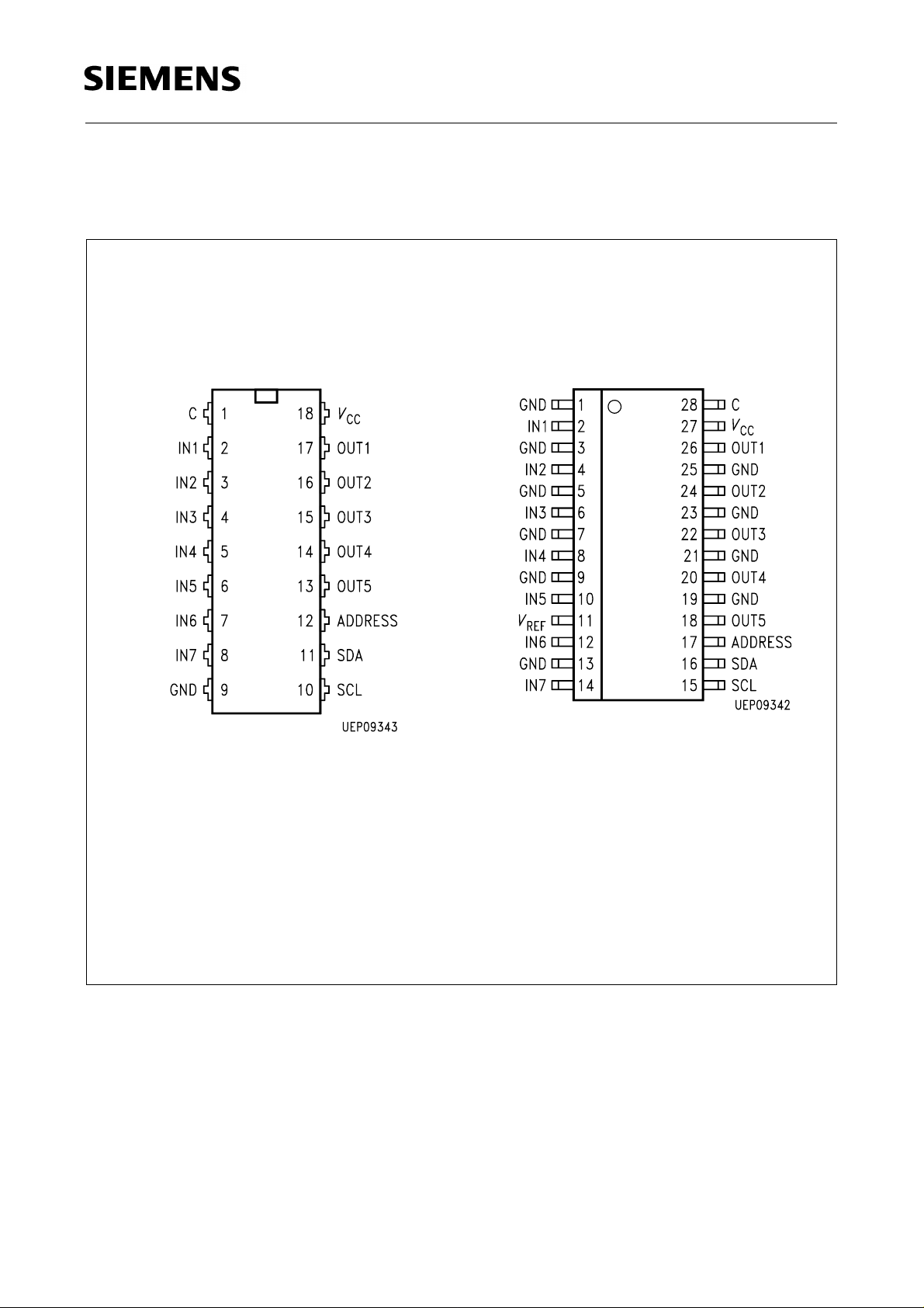
1.4 Pin Configuration
(top view)
P-DIP-18-5 P-DSO-28-1
TDA 6920
Figure 1
Semiconductor Group 2
1.5 Pin Definitions and Functions
Pin No. Symbol Function
P-DIP-18-5 P-DSO-28-1
– 1 GND Signal and power supply ground
2 2 IN1 CVBS input 1
– 3 GND Signal and power supply ground
3 4 IN2 CVBS input 2
– 5 GND Signal and power supply ground
4 6 IN3 CVBS input 3
– 7 GND Signal and power supply ground
5 8 IN4 CVBS input 4
TDA 6920
– 9 GND Signal and power supply ground
6 10 IN5 CVBS input 5
–11
V
REF
Reference Voltage for external use
7 12 IN6 CVBS input 6
9 13 GND Power supply groung
8 14 IN7 CVBS input 7
10 15 SCL I
11 16 SDA I
2
C-Bus clock
2
C-Bus data
12 17 ADDRESS Address selection
13 18 OUT5 CVBS output 5
– 19 GND Signal and power supply ground
14 20 OUT4 CVBS output 4
– 21 GND Signal and power supply ground
15 22 OUT3 CVBS output 3
– 23 GND Signal and power supply ground
16 24 OUT2 CVBS output 2
– 25 GND Signal and power supply ground
17 26 OUT1 CVBS output 1
18 27
V
CC
Positive power supply voltage
1 28 C Separate color adding input for input 1
Semiconductor Group 3
1.6 Pin Description
TDA 6920
Overview
C (color input)
In 2, 5, 6, 7 (CVBS input)
In 2, 3, 4 (CVBS input)
SCL, Address
Semiconductor Group 4
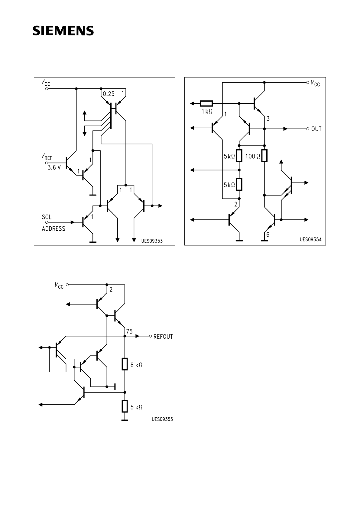
TDA 6920
Overview
SDA
Out 1-5 (CVBS output)
V
(SO-28 only)
REF
Semiconductor Group 5
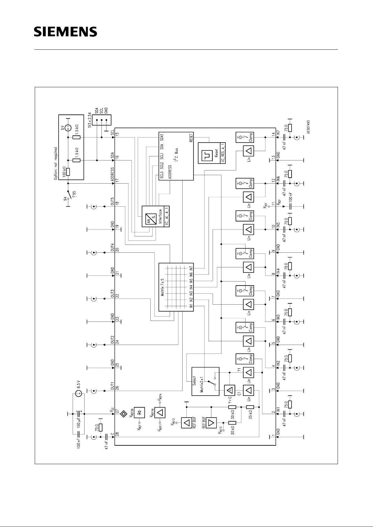
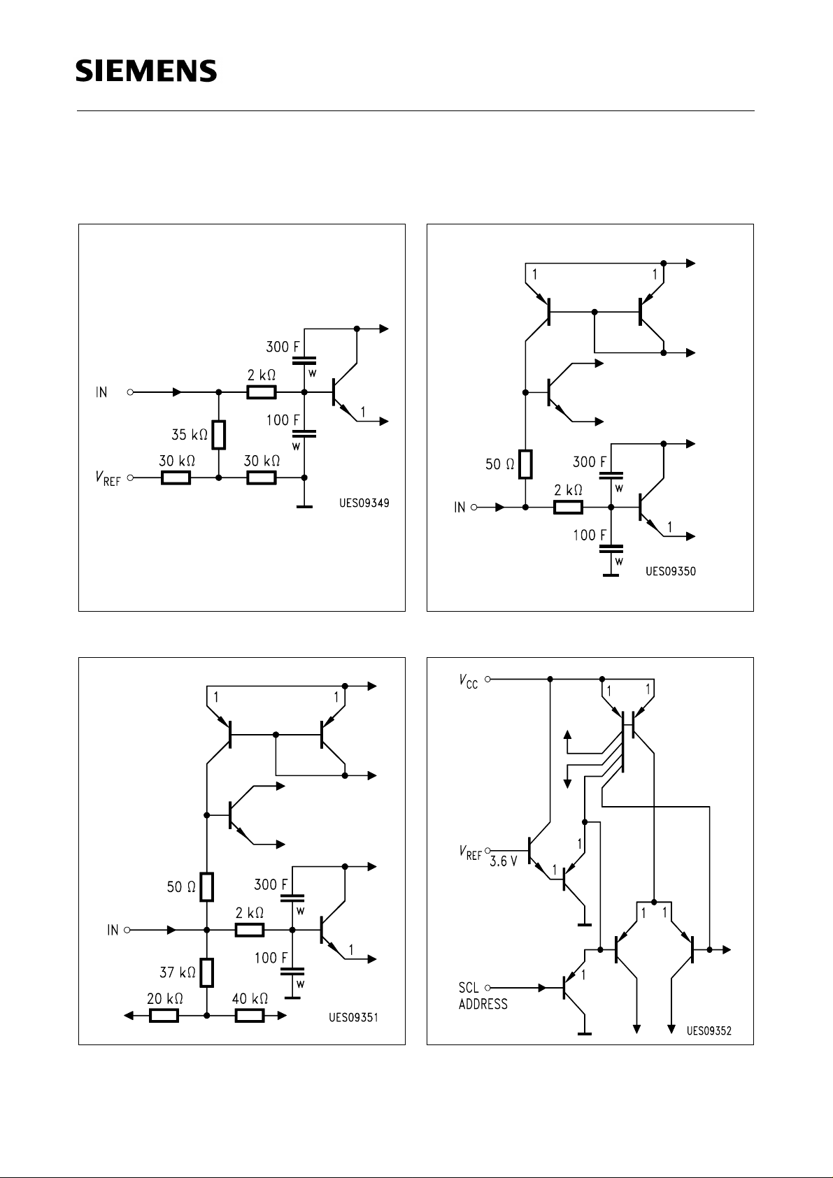
1.7 Functional Block Diagram
TDA 6920
Figure 2
Block Diagram (P-DSO-28-1)
Semiconductor Group 6
 Loading...