

Siemens TDA5666-5 Datasheet
Video Modulator for
TDA 5666-5
FM-Audio
Preliminary Data Bipolar IC
Features
● FM-audio modulator
● Sync level clamping of video input signal
● Controlling of peak white value
● Continuous adjustment of modulation depth for
positive or negative values
● Symmetrical mixer output with separate ground area
● Symmetrical oscillator with separate RF-ground
● Low spurious radiation
● High stability of the RF-oscillator frequency
● High stability of the audio oscillator
● Internal reference voltage
● 12 V supply voltage
P-DIP-18 -5
Type Ordering Code Package
TDA 5666-5 Q67000-A5168 P-DIP-18-5
Functional Description and Application
The monolitic integrated circuit TDA 5666-5 is especially suitable as a modulator for the
48- to 860-MHz frequency range.
Video recorders, cable converters, TV-converter networks, demodulators, video
generators, video security systems, amateur TV-applications and personal computers.
Semiconductor Group 1 02.95

TDA 5666-5
Circuit Description
Oscillator
The RF-oscillator is available at pins 3-7. The oscillator operates as a symmetrical
Colpitts circuit. The oscillator chip ground, pin 5, should be connected to ground at the
resonance circuit shielding point. An external oscillator can be injected inductively or
capacitively via pins 3 and 7. The layout of the PCB should be such as to provide a
minimum shielding attenuation between the oscillator pins 3-7 and modulator output pins
13-15 of approximately 80 dB.
For optimal residual carrier suppression, the symmetrical mixer outputs at pins 13, 15
should be connected to a matched balanced-to-unbalanced broadband transformer, e.g.
a Guanella transformer with good phase precision at 0
should be less than 3 dB. In addition, an LC-low pass filter combination is required at the
output. The cut-off frequency of the low pass filter combination must exceed the
maximum operating frequency.
o
and 180o. The transmission loss
Video
The video signal with the negative synchronous level is capacitively connected to pin 10.
The internal clamping circuit is referenced to the synchronizing level. Should the video
signal change by 6 dB, this change will be compensated by the resonance circuit which
is set by the peak white value. At pin 11, the current pulses of the peak white detector are
filtered through the capacitor which also determines the control time constant. The RFcarrier switches from negative to positive video modulation, when pin 12 is connected
to ground. By varying the value of resistanceR at pin 12 between
∞ ... 0Ω the modulation
depth can be increased from 70% to 100% when the modulation is negative and
decreased from 100% to 70% when the modulation is positive.
Audio
Via pin 1, the audio signal is capacitively coupled to the AF-input for the FM-modulation
of the oscillator. A parallel resonance circuit is connected to the audio carrier oscillator at
pins 17, 18. The unloaded Q of the resonant circuit must be Q = 25 and the parallel
resistor R
= 8.2 kΩ to ensure a video to audio carrier ratio of 12.5 dB. At the same time,
T
the capacitative and/or inductive reactance for the resonance frequency should have a
value of X
≈ XL≈ 800 Ω.
C
The video to audio carrier ratio can be changed by connecting an external voltage to pin
16, which deviates from the internal reference voltage.
At the output of the above described mixer the FM modulated audio signal is added to
the video signal and mixed with the oscillator signal in the RF-mixer.
Source
The internal reference voltage is available at pin 2 and has to be capacitively blocked
there.
Semiconductor Group 2
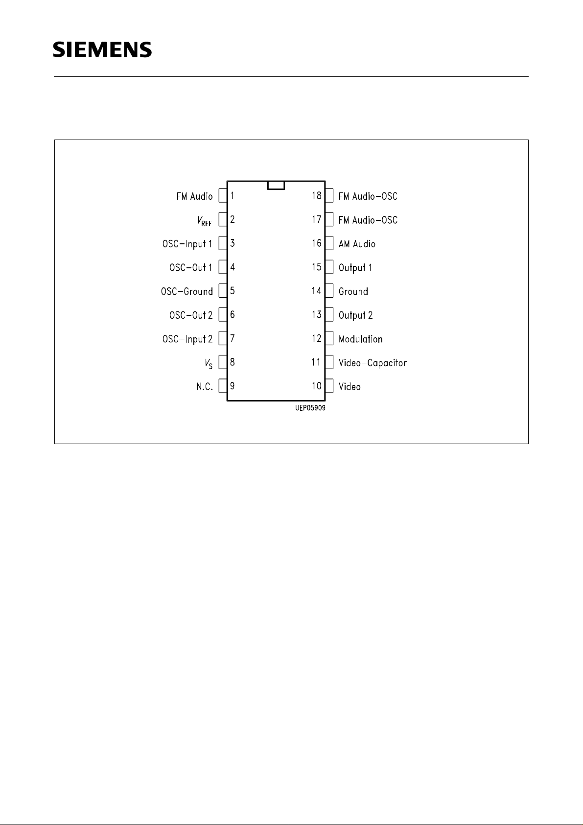
Pin Configuration
(top view)
TDA 5666-5
Semiconductor Group 3

Pin Definitions and Functions
Pin No. Symbol Function
1 FM-Audio AF-input for FM-modulation
TDA 5666-5
2 V
REF
Internal reference voltage (7.5 V)
3 OSC-Input 1 Symmetrical oscillator input
4 OSC-Out 1 Symmetrical oscillator output
5 OSC-Ground Oscillator ground
6 OSC-Out 2 Symmetrical oscillator output
7 OSC-Input 2 Symmetrical oscillator input
8 V
S
Supply voltage (12 V)
9 N.C. Not connected
10 Video Video input with clamping
11 Video-Capacitor Connection for smoothing capacitor for video control
loop
12 Modulation Switch-over for positive and negative modulation
13 Output 2 Symmetrical RF-output
14 Ground Ground
15 Output 1 Symmetrical RF-output
16 Audio carrier ratio Video to audio carrier ratio adjustment
17 FM-Audio OSC FM-audio oscillator; symmetrical inputs for tank circuit
18 FM-Audio OSC FM-audio oscillator; symmetrical inputs for tank circuit
Semiconductor Group 4
TDA 5666-5
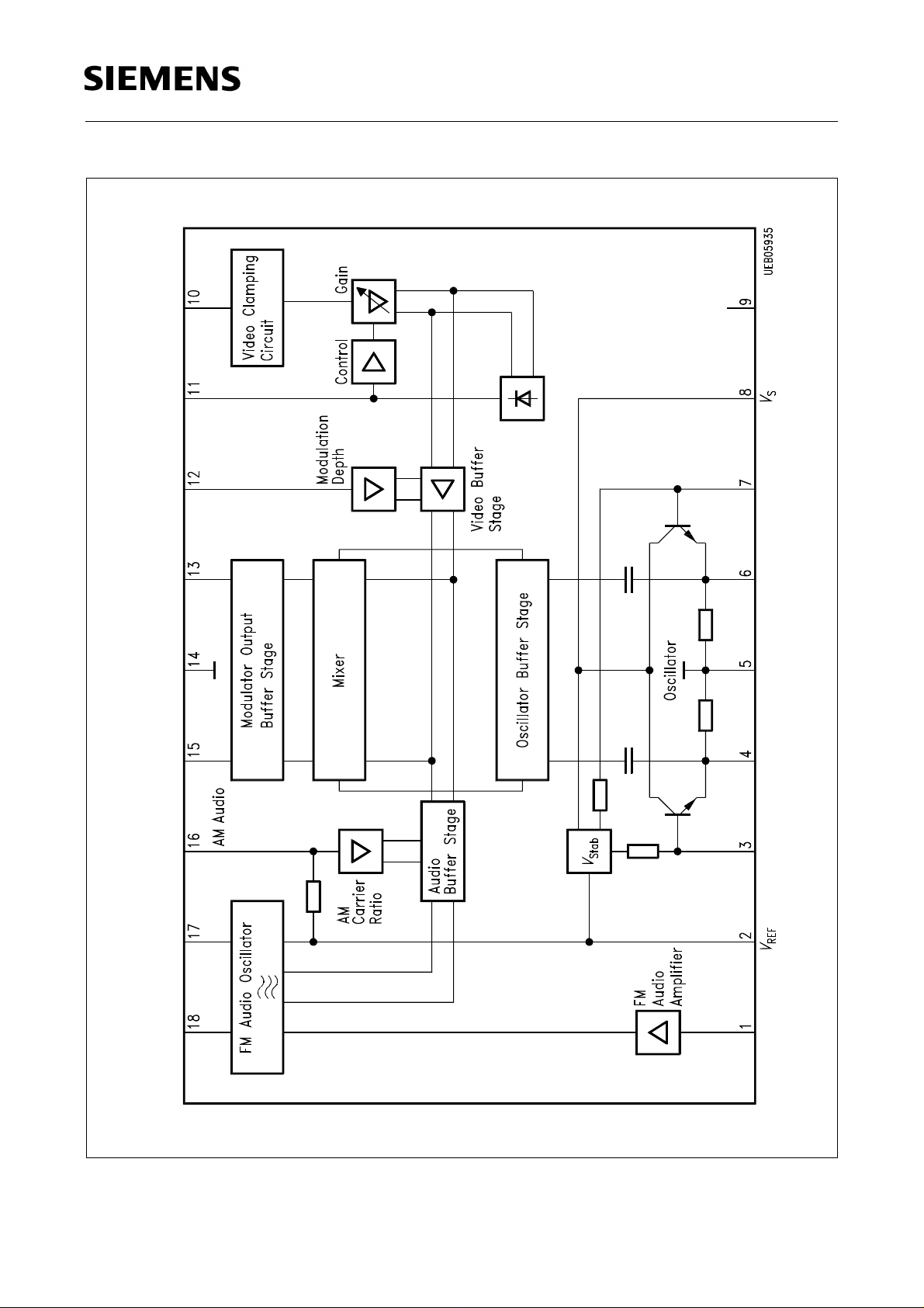
Block Diagram
Semiconductor Group 5
TDA 5666-5
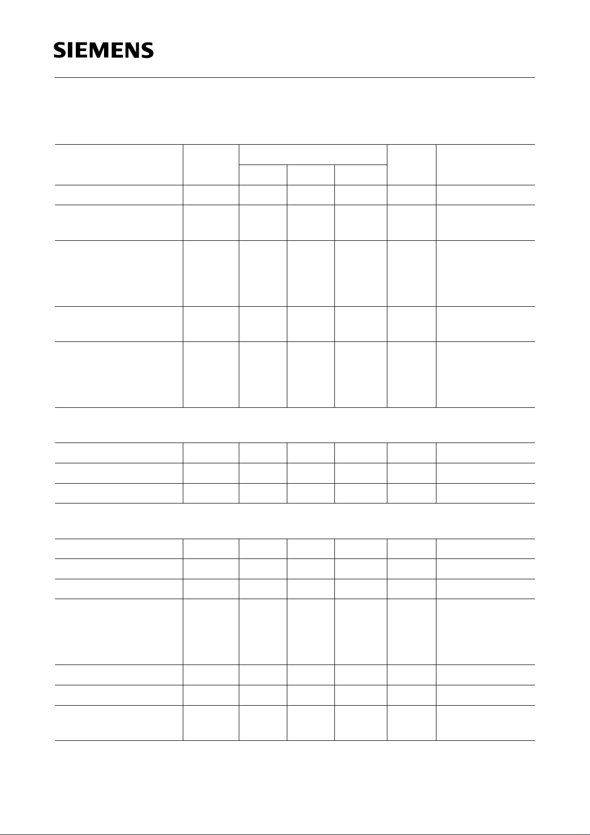
Absolute Maximum Ratings
T
= 0 to 70oC
A
Parameter Symbol Limit Values Unit Remarks
min. typ. max.
Supply voltage pin 8 V
Current from pin 2 –I
Voltage at pin 1
Voltage at pin 2
Voltage at pin 10
V
V
V
S
2
1
2
10
– 0.3 14.5 V
02mAV
0
6
0
2
8.5
1.5
V
V
Vpp only via C
= 7-8 V
2
V
= 10-13.5 V
S
(max. 1 µF)
Capacitance at pin 2
Capacitance at pin 11
Voltage at pin 12
Voltage at pin 13
Voltage at pin 15
Voltage at pin 16
C
C
V
V
V
V
2
11
12
13
15
16
0
0
– 0.3
V
2
V
2
V2-1.5
100
15
1.4
V
S
V
S
VS+1.5
nF
µF
V
V
V
V V
= 10-13.5 V
S
According to the application circuit, only the provided circuitry can be connected
to pins 3,4,6,7,17 and 18.
Junction temperature T
Storage temperature T
j
stg
150
– 40 125
o
C
o
C
Thermal resistance R
Operating Range
Supply voltage V
Video input frequency f
Audio input frequency f
Output frequency f
Ambient temperature T
Audio oscillator f
Voltage at pin 2
Voltage at pin 13,15
th
S
Video
AF
Q
A
OSC
V
2
V
13, 15
80 K/W
10 13.5 V
0 6 MHz
0 20 kHz
30 860 MHz depending on
the oscillator
circuitry at
pins 3-7
070
o
C
4 7 MHz
6.75
V
2
7.75
V
S
V
V
Semiconductor Group 6
AC/DC-Characteristics
T
= 25oC; VS = 12 V
A
Parameter Symbol Limit Values Unit Test
min. typ. max.
Condition
Source
TDA 5666-5
Test
Circuit
Current consumption
Current consumption
Reference voltage V
I
8
I13 + I
2
Oscillator
Oscillator frequency
f
OSC
range
Switch-on, warm up drift; (T
C
selfheating of the component.
∆ f
OSC
Frequency drift as
function of V
S
RF-output
∆ f
OSC
R
13;R15
impedance
C13 = C
15
15
2.0
20
2.6
26
3.4
mA
mA
I2 = 0 mA 1
6.75 7.25 7.75 V 0 ≤ I2≤ 1 mA 1
30 860 MHz external circuitry
adjusted to
frequency
-value of capacitor in osc. circuit is 0) drift is referenced only to
0
0
– 50
– 200
– 500
– 500
kHz
Ch 30
kHz
t = 0.5-10 s;
TA = const.
Ch 40
–150 150 kHz VS= 10-13.5 V
TA = const.;
Ch 40
10
kΩ
parallel
equivalent circuit
0.5 1 2.0
15
pF
parallel
equivalent circuit
1
1
1
1
1
RF-output voltage V
RF-output phase α
RF-output voltage
Q
13, 15
∆V
Q
2.5 4.5 5.5 mVrms Ch 40; video
140 180 220 deg
0
changes
Intermodulation ratio α
Harmonic wave ratio α
∆V
∆V
Q
Q
IMR
O
0
0
50 75 dB fVC + 1.07 MHz 2
35 dB fVC + 8.8 MHz
Semiconductor Group 7
1.5
1.5
1.5
dB
dB
dB
100% white;
without audiosignal
f = 543-623 MHz
Ch 30...40
f = 100-300 MHz
f = 48-100 MHz
without video
1
1
1
1
2
 Loading...