

查询TDA 4601供应商
Control ICs for Switched-Mode Power Supplies
Features
● Direct control of the switching transistor
● Low start-up current
● Reversing linear overload characteristic
● Base current drive proportional to collector current
● Protective circuit in case of disturbance
TDA 4601
Bipolar IC
P-SIP-9-1
Type Ordering Code Package
TDA 4601 Q67000-A2379 P-SIP-9-1
The integrated circuit TDA 4601/D is designed for driving, controlling and protecting the switching
transistor in self-oscillating flyback converter power supplies as well as for protecting the overall
power supply unit. In case of disturbance, the rise of the secondary voltage is prevented. In addition
to the ICs application range including TV-receivers video tape recorders, hifi devices and active
loudspeakers, it can also be used in power supply units for professional applications due to its wide
control range and high voltage stability during increased load changes.
Semiconductor Group 7 06.94
Pin Definitions and Functions
Pin No. Function
TDA 4601
1
2 Zero passage identification
3 Input control amplifier, overload amplifier
4 Collector current simulation
5 Connection for additional protective circuit
6 Ground (rigidly connected to substrate mounting plate)
7 DC-output for charging coupling capacitor
8 Pulse output - driving of switching transistor
9 Supply voltage
V
REF
output
Block Diagram
Semiconductor Group 8

TDA 4601
Circuit Description
The TDA 4601 is designed for driving, controlling and protecting the switching transistor in flyback
converter power supplies during start-up, normal and overload operations as well as during
disturbed operation. In case of disturbance the drive of the switching transistor is inhibited and a
secondary voltage rise is prevented.
Start-Up
The start-up procedures (on-mode) include three consecutive operating phases as follows:
1. Build-Up of Internal Reference Voltage
The internal reference voltage supplies the voltage regulator and effects charging of the coupling
electrolytic capacitor connected to the switching transistor. Current consumption will remain at
I
< 3.2 mA with a supply voltage up to V9 approx. 12 V.
9
2. Enabling of Internal Voltage - Reference Voltage V1 = 4 V
Simultaneously with V9 reaching approx. 12 V, an internal voltage becomes available, providing
all component elements, with the exception of the control logic, with a thermally stable and
overload-resistant current supply.
3. Enabling of Control Logic
In conjunction with the generation of the reference voltage, the current supply for the control logic
is activated by means of an additional stabilization circuit. The integrated circuit is then ready for
operation.
The start-up phase above described are necessary for ensuring the charging of the coupling
electrolytic capacitor, which in turn supplies the switching transistor. Only then is it possible to
ensure that the transistor switches accurately.
Normal Operating Mode / Control Operating Mode
At the input of pin 2 the zero passages of the frequency provided by the feedback coil are registered
and forwarded to the control logic. Pin 3 (control input, overload and standby identification) receives
the rectified amplitude fluctuations of the feedback coil. The control amplifier operates with an input
voltage of approx. 2 V and a current of approx. 1.4 mA. Depending on the internal voltage reference,
the overload identification limits inconjunction with collector current simulator pin 4 the operating
range of the control amplifier. The collector current is simulated by an external RC-combination
present at pin 4 and internally set threshold voltages. The largest possible collector current
applicable to the switching transistor (point of return) increases in proportion to the increased
capacitance (10 nF). Thus the required operating range of the control amplifier is established. The
range of control lies between a DC-voltage clamped at 2 V and a sawtooth - shaped rising ACvoltage, which can vary up to a max. amplitude of 4 V (reference voltage). During secondary load
reduction to approx. 20 W, the switching frequency is increased (approx. 50 kHz) at an almost
constant pulse duty factor (1:3). During additional secondary load decreases to approx. 1 W, the
switching frequency increases to approx. 70 kHz and pulse duty factor to approx. 1:11. At the same
time collector peak current is reduced to < 1 A.
Semiconductor Group 9

TDA 4601
The output levels of the control amplifier as well as those of the overload identification and collector
current simulator are compared in the trigger and forwarded to the control logic. Via pin 5 it is
possible to externally inhibit the operations of the IC. The output at pin
V
REF
pin 8 will be inhibited when voltages of ≤ – 0.1 are present at pin 5.
Flipflops for controlling the base current amplifier and the base current shut-down are set in the
control logic depending on the start-up circuit, the zero passage identification as well as on the
enabling by the trigger. The base current amplifier forwards the sawtoothspahed
output of pin 8. A current feedback with an external resistor (R = 0.68 Ω) is present between pin 8
and pin 7. The applied value of the resistor determines the max. amplitude of the base driving
current for the switching transistor.
Protective Operating Mode
The base current shut-down activated by the control logic clamps the output of pin 7 to 1.6 V. As a
result, the drive of the switching transistor is inhibited. This protective measure is enabled if the
supply voltage at pin 9 reaches a value ≤ 6.7 V or if voltages of
------------
2
V
voltage to the
4
V
REF
------------
≤ – 0.1 are present at pin 5.
2
In case of short-circuits occurring in the secondary windings of the switched-mode power supply,
the integrated circuit continuously monitors the fault conditions. During secondary, completely loadfree operation only a small pulse duty factor is set. As a result the total power consumption of the
power supply is held at
inhibited for a voltage supply of ≤ 6.7 V, the reference voltage (4 V) is switched off if the voltage
supply is further reduced by ∆V9= 0.6 V.
Protective Operating Mode at Pin 5 in Case of Disturbance
The protection against disturbances such as primary undervoltages and/or secondary overvoltages (e.g. by changes in the component parameters for the switched-mode power supply) is
realized as follows:
Protective Operating Mode with Continuous Fault Condition Monitoring
In case of disturbance the output pulses at pin 8 are inhibited by falling below the protective
threshold V5, with a typical value of V1/2. As a result current consumption is reduced (I9≥ 14 mA
at V9=10V).
With a corresponding high-impedance start-up resistor *), supply voltage V9 will fall below the
minimum shut-down threshold (5.7 V) for reference voltage V1. V1 will be switched off and current
consumption is further reduced to I9≤ 3.2 mA at V9≤ 10 V.
N = 6 ... 10 W during both operating modes. After the output has been
Because of these reductions in current consumption, the supply voltage can rise again to reach the
switch-on threshold of V9≥ 12.3 V. The protective threshold at pin 5 is released and the power
supply is again ready for operation.
Semiconductor Group 10

TDA 4601
In case of continuing problems of disturbance (V5≤ V1/2 – 0.1 V) the switch-on mode is interrupted
by the periodic protective operating mode described above, i.e. pin 8 is inhibited and V9 is falling,
etc.
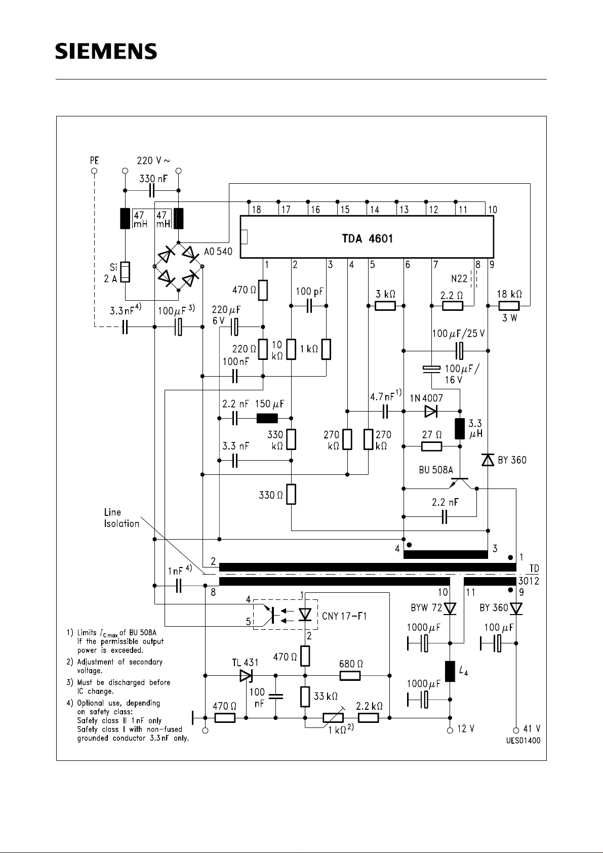
Switch-On in the Wide Range Power Supply (90 Vac to 270 Vac)
(application circuit 2)
Self-oscillating flyback-converters designed as wide range power supplies require a power source
independent of the rectified line voltage for TDA 4601. Therefore the winding polarity of winding
11/13 corresponds to the secondary side of the flyback converter transformer. Start-up is not as
smooth as with an immediately available supply voltage, because TDA 4601 has to be supplied by
the start-up circuit until the entire secondary load has been charged. This leads to long switch-on
times, especially if low line voltages are applied.
However, the switch-on time can be shortened by applying the special start-up circuit (dotted line).
The uncontrolled phase of feedback control winding 15/9 is used for activating purposes.
Subsequent to activation, the transistor T1 begins to block when winding 11/13 generates the
current supply for TDA 4601. Therefore, the control circuit cannot be influenced during operation.
Semiconductor Group 11

Absolute Maximum Ratings
Parameter Symbol Limit Values Unit
min. max.
TDA 4601
Supply voltage
Voltages
Reference output V
Zero passage identification
Control amplifier
Collector current simulation
Blocking input
Base current cut-off point
Base current amplifier output
Currents
Zero passage identification I
Control amplifier
Collector current simulation
Blocking input
Base current cut-off point
Base current amplifier output
Junction temperature
Storage temperature range
Thermal resistances:
system-air TDA 4601
system-case TDA 4601
system-air
system-case
1)
2)
TDA 4601-D
TDA 4601-D
V
9
1
V
2
V
3
V
4
V
5
V
7
V
8
l i2
I
l 3
I
l 4
I
l 5
I
Q 7
I
Q 8
T
j
T
stg
R
th SA
R
th SC
R
th SA
R
th SA1
020V
06V
– 0.6 0.6 V
03V
08V
08V
0 V
0 V
9
9
V
V
–5 5 mA
– 3 3 mA
05mA
05mA
– 1 1.5 A
– 1.5 0 A
125 ˚C
– 40 125 ˚C
70
15
60
44
K/W
K/W
K/W
K/W
Semiconductor Group 12

Absolute Maximum Ratings (cont’d)
Parameter Symbol Limit Values Unit
min. max.
Operating Range
TDA 4601
Supply voltage
Case temperature TDA 4601
Ambient temperature range
1) Case soldered on PC-board without cooling surface
2) Case soldered on PC-board with copper-clad 35 µm layer, cooling surface 25 cm
3) R
= 44 K/W and PV = 1 W
th SA1
3)
TDA 4601-D T
V
9
T
C
A
7.8 18 V
085˚C
070˚C
2
Semiconductor Group 13

TDA 4601
Characteristics
T
= 25 ˚C
A
according to measurement circuit 1 and diagram
Parameter Symbol Limit Values Unit
min. typ. max.
Start Operation
Current consumption (V1 not yet
switched on)
V
= 2 V
9
V
= 5 V
9
V
= 10 V
9
Switching point for
V
1
I
9
I
9
I
9
V
9
11.0 11.8 12.3 V
1.5
2.4
0.5
2.0
3.2
mA
mA
mA
Normal Operation
V
= 10 V; V
9
= – 10 V; V
cont
= ± 0.5 V; f = 20 kHz
clock
duty cycle 1:2 after switch-on
Current consumtion
V
= – 10 V
cont
V
= 0 V
cont
Reference voltage
I
< 0.1 mA
1
I
< 5 mA
1
Temperature coeffiecient of
reference voltage
Control voltage
V
= 0 V V
cont
Collector current simulation voltage
V
= 0 V
cont
V
= 0 V/– 10 V
cont
Clamping voltage
Output voltages
V
= 0 V
cont
V
= 0 V
cont
V
= 0 V/– 10 V
cont
Feedback voltage
I
9
I
9
V
1
V
1
TC
1
3
)
V
*
4
∆V4*
V
5
V
Q7
V
Q8
∆V
Q8
V
*
2
110
50
4.0
4.0
–10
135
75
4.2
4.2
– 3
160
100
4.5
4.5
mA
mA
V
V
1/K
2.3 2.6 2.9 V
1.8
)
0.3
2.2
0.4
2.5
0.5
V
V
6.0 7.0 8.0 V
)
*
*
)
2.7
)
2.7
1.6
3.3
3.4
2.0
4.0
4.0
2.4
V
V
V
0.2 V
*) DC-component only
Semiconductor Group 14

TDA 4601
Protective Operation
V
= 10 V; V
9
duty cycle 1:2
Parameter Symbol Limit Values Unit
Current consumption
V
< 1.9 V I
5
Switch-off voltage
V
< 1.9 V V
5
Switch-off voltage
V
< 1.9 V V
5
Blocking input
Blocking voltage
V
= 0 V V
cont
Supply voltage blocked for
V
= 0 V
cont
V
off (with further reduction of V9) ∆V
1
= – 10 V; V
cont
= 0.5 V; f = 20 kHz;
clock
9
Q 7
4
5
V
8
V
4
9
min. typ. max.
14 22 28 mA
1.3 1.5 1.8 V
1.8 2.1 2.5 V
V
1
------ 0.1–
2
V
------
1
2
V
6.7 7.4 7.8 V
0.3 0.6 1.0 V
Characteristics
T
= 25 ˚C; according to measurement circuit 2
A
Parameter Symbol Limit Values Unit
min. typ. max.
Switching time (secondary voltage)
t
ON
350 450 ms
Voltage variation S3 = closed
∆
N
= 20 W ∆V
3
2 sec
100 500 mV
Voltage variation S2 = closed
N
= 15 W ∆V
∆
3
2 sec
500 1000 mV
Standby operation S1 = open
secondary useful load = 3 W ∆
V
2 sec
f 70
20
75
30
–
V
kHz
The cooling conditions have to be optimized with regard to maximum ratings
(TA; Tj; R
th JC
; R
th SA
).
Semiconductor Group 15

TDA 4601
Circuit Diagram
Semiconductor Group 16
TDA 4601
Test and Measurement Circuit 1
Test Diagram: Overload Operation
Semiconductor Group 17

Wide range from 80 to 270 Vac
TDA 4601
Application Circuit 2
Semiconductor Group 18

TDA 4601
Notes on Application Circuit 2
Wide Range SMPS
Filtering of the rectified AC-voltage has been increased up to 470µF to ensure a constant and humfree supply at V
good start-up conditions for the SMPS in the low voltage range, the non-stabilized phase of winding
13/15 is used as a starting aid (BD 139), which is turned off after start-up by means of Z-diode C12.
In comparison to the 220 Vac standard circuit, however, the collector-emitter circuit had to be
altered to improve the switching behavior of BU 208 for the entire voltage range (80 to 270 Vac).
Diode BY 231 is necessary to prevent inverse operation of BU 208 and may be integrated for
switching times with a secondary power < 75 W (BU 208 D).
Compared to the IC TDA 4600-2, the TDA 4601 has been improved in turn-off during under-voltage
at pin 5. The TDA 4601 is additionally provided with a differential amplifier input at pin 5, enabling
precise turn-off at the output of pin 8 accompanied by hysteresis. For wide range SMPS, TDA 4601
is recommendable instead of TDA 4600-2. If a constant quality standard equal to that of the
standard circuit is to be maintained, wide range SMPS (80 to 270 Vac) with secondary power of
120 W can only be implemented at the expense of time.
= 80 Vac. The stabilized phase is tapped for supplying the IC. In order to ensure
line
Semiconductor Group 19

Supplements to Application Circuit 2
Efficiency versus Output Power
TDA 4601
Efficiency versus Output Power
Semiconductor Group 20

Supplements to Application Circuit 2
TDA 4601
Load Characteristics V
2sec
= f (I
2sec
)
Output Voltage V
(line change)
2sec
Semiconductor Group 21

Further Applications
TDA 4601
Application Circuit 3
Semiconductor Group 22

TDA 4601
Notes on Application Circuit 3
Fully Insulated, Clamp-contacted PTC-Thermistor Suitable for SMPS-Applications at
Increased Start-Up Currents
The newly developed PTC-thermistor Q63100-P2462-J29 is designed for applications in SMPS as
well as in various other electronic circuits, which, for example, receive the supply voltage directly
from the rectified line voltage and require an increased current during turn-on. Used in the flyback
converter power supply of TV-sets, an application proved millions of times over, the new PTCthermistor in the auxiliary circuit branch has resulted in a power saving of no less than 2 W. This
increase in efficiency has a highly favorable effect on the standby operation of TV-sets.
The required turn-on current needs only 6 to 8 s until the operating temperature of the PTCthermistor is reached. Low thermal capacitance of the PTC-thermistor allows the circuit to be
operated again after no more than 2 s. Another positive feature is the improved short-circuit
strength. The clamp contacts permit more or less unlimited switching operations and thus
guarantee high reliability. A flame-retardant plastic package and small dimensions are additional
advantages of this newly developed PTC-thermistor.
Technical Data
Parameter Symbol Limit Values Unit
Breakdown voltage at
Resistance at
T
A
Resistance tolerance ∆
Trip current (typ.)
Residual current at
Max. application voltage
Reference temperature (typ.)
Temperature coefficient (typ.)
Max. operating current
Storage temperature range
T
= 60 ˚C V
A
= 25 ˚C R
V
A max
BD rms
25
R
25
I
K
I
R
V
op max rms
T
REF
T
C
I
max
T
stg
350 V
5kΩ
25 %
20 mA
2mA
265 V
190 ˚C
26 %/K
0.1 A
– 25 to 125 ˚C
Semiconductor Group 23
TDA 4601
Application Circuit 4
Semiconductor Group 24

TDA 4601
Notes on Application Circuit 4
Improved Load Control and Short-Circuit Characteristics
Turn-on is the same as for circuit 3.
To make the price more attractive, switching transistor BU 508 A was selected.
To ensure optimum standby conditions, the capacitance between pins 2 and 3 was increased to
100 pF.
Z- diode C
Design and coupling conditions of various flyback transformers were sometimes a reason for
overshoot spectra, which, despite the RC-attenuating element 33 Ω x 22 nF and the 10-kΩ resistor,
even penetrated across the feedback winding 9/15 to the zero passage indicator input (pin 2) and
activated double and multiple pulses in the IC. Double and multiple pulses, however, lead to
magnetic saturation in the flyback transformer and thus increase the risk of damaging the switchedmode power supply.
The larger the quantities of power to be passed, the more easily overshoots are generated. This
can be observed around the point of return. The switched-mode power supply, however, reduces
its own power to a minimum in all cases of overload or short-circuit. A series resonant circuit, whose
resonance corresponds to the transformer’s selfoscillation, was created by combination of the
4.7-µH inductance and the 22-nF capacitance. This resonant circuit short-circuits overshoots via a
33-Ω resistor.
transfers control voltage ∆V
6.2
directly to pin 3 resulting in improved load control.
cont
f
1
-----------------
2π LC
500 kHz≈=
Semiconductor Group 25
TDA 4601
Application Circuit 5
Semiconductor Group 26

TDA 4601
Notes on Application Circuit 5
Highly Stable Secondary Side
Power supplies for commercial purposes require highly constant low voltages and high currents
which, on the basis of the flyback converter principle, can be realized only under certain conditions,
but, on the other hand, are implemented for economical reasons. An electrically isolated flyback
converter with a highly stable secondary side must receive the control information from this
secondary side. There are only two possibilities for meeting this requirement: either through a
transformer which is magnetically isolated from the flyback converter or by means of an
optocoupler. The development of CNY 17 has enabled the manufacture of a component suitable for
electrical isolation and characterized by high reliability and long-term stability.
The IC TDA 4601-D is the sucessor of the TDA 4600-D. It is compatible with its predecessor in all
operational functions and in the control of a self-oscillating flyback converter. Pin 3 is the input for
the control information, where the latter is compared with the reference voltage prevailing at pin 1
and the control from the optocoupler and subsequently transformed into a frequency/pulse width
control.
The previous feedback and control information winding is not necessary. The feedback information
(zero passage) is obtained from winding 3/4 - supply winding. The time constant chain 330 Ω/3.3 nF
and 330 Ω/2.2 nF was implemented in series with 150 µH to prevent interference at pin 2. The LCelement forms a series resonant circuit for overshoots of the flyback converter and short-circuits
them.
Semiconductor Group 27

TDA 4601
Application Circuit 6
Semiconductor Group 28

TDA 4601
Notes on Application Circuit 6
Wide Range Plug SMPS up to 30 W
Due to their volume and weight, plug SMPS have so far been limited to a restricted primary voltage
and a secondary power of no more than 6 W.
The line-isolated wide range flyback converter presented here has a variable frequency and is
capable of producing a secondary power of 30 W. It is characterized by a compact design with an
approx. weight of 400 g. The entire line voltage range of 90 to 260 Vac is stabilized to ± 1.5 % on
the secondary side. Load fluctuations between 0.1 and 2 A are regulated to within 5 %. The output
(secondary side) is overload, short-circuit, and openloop proof.
Semiconductor Group 29

TDA 4601
Application Circuit 7
Semiconductor Group 30

Notes on Application Circuit 7
TDA 4601
Wide Range SMPS with Reducing Peak Collector Current I
CBU208
for Rising Line Voltage
(variable point of return)
Wide range SMPS have to be dimensioned at line voltages of 90 to 260 Vac. The difference
between the maximum collector current I
I
C BU 208 limit
which causes magnetic saturation of the flyback transformer and flows through the
C BU 208 max
primary inductance winding 5/7 is to be determined at Vac
Then, the transmissible power of the flyback transformer and its value at Vac
In the standard circuit the collector current I
C BU 208 max
and the largest possible limit current
min
(I
C BU 208 limit
≥ 1.2 x I
is to be determined.
max
C BU 208 max
is almost constant at the point of return
independent of the line voltage. The transmissible power on the secondary side, however,
increases at the point of return in proportion to the rising rectified line voltage applied (figures 1 and
2).
In the wide range SMPS a line voltage ratio of 270/90 = 3/1 is obtained, causing doubling of the
transmissible power on the secondary side, i.e. in the wide range SMPS a far too large flyback
transformer had to be implemented.
The point of return protecting the SMPS against overloads or short circuits, is derived from the time
constant at pin 4t4 = 270 kΩ x 4.7 nF. Thus, the largest possible pulse width is determined.
With the introduction of the 33-kΩ resistor this time constant is reduced as a function of the control
voltage applied to winding 13/15, rectified by diode BY 360 and filtered by the 1-µF capacitance,
which means that the pulse time becomes shorter. By means of the Z-diode
C
the line voltage
18
level can be defined at which the influence of the time constant correction becomes noticeable. The
change in the rectified voltage of winding 13/15 is proportional to the change in the rectified line
voltage.
).
At the point of return I
CBU208
the peak collector current has been reduced with the aid of the given
values from 5.2 A at 90 Vac to 3.3 A at 270 Vac. The transmissible power at the point of return
remains stable between 125 and 270 Vac due to the set activation point of the point of return
correction (unbroken curve in figure 2).
Semiconductor Group 31

Load Characteristics
TDA 4601
Figure 1
Figure 2
Semiconductor Group 32
 Loading...