

Siemens TCA785 Datasheet
TCA 785
Phase Control IC TCA 785
Bipolar IC
Features
● Reliable recognition of zero passage
● Large application scope
● May be used as zero point switch
● LSL compatible
● Three-phase operation possible (3 ICs)
● Output current 250 mA
● Large ramp current range
● Wide temperature range
Type Ordering Code Package
P-DIP-16-1
TCA 785 Q67000-A2321 P-DIP-16-1
This phase control IC is intended to control thyristors, triacs, and transistors. The trigger pulses
can be shifted within a phase angle between 0 ˚ and 180 ˚. Typical applications include
converter circuits, AC controllers and three-phase current controllers.
This IC replaces the previous types TCA 780 and TCA 780 D.
Pin Definitions and Functions
Pin Symbol Function
1 GND Ground
2
3
4
5 V
6
7
8 V
Q2
Q U
Q2
SYNC Synchronous voltage
I
Q Z
REF Stabilized voltage
Output 2 inverted
Output U
Output 1 inverted
Inhibit
Output Z
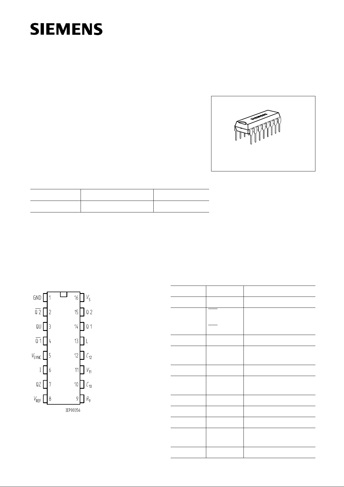
Pin Configuration
(top view)
Semiconductor Group 1
9
10
R
9
C10
Ramp resistance
Ramp capacitance
11 V11 Control voltage
12 C
12 Pulse extension
13 L Long pulse
14
15
16 V
Q 1
Q 2
S Supply voltage
Output 1
Output 2
09.94
TCA 785
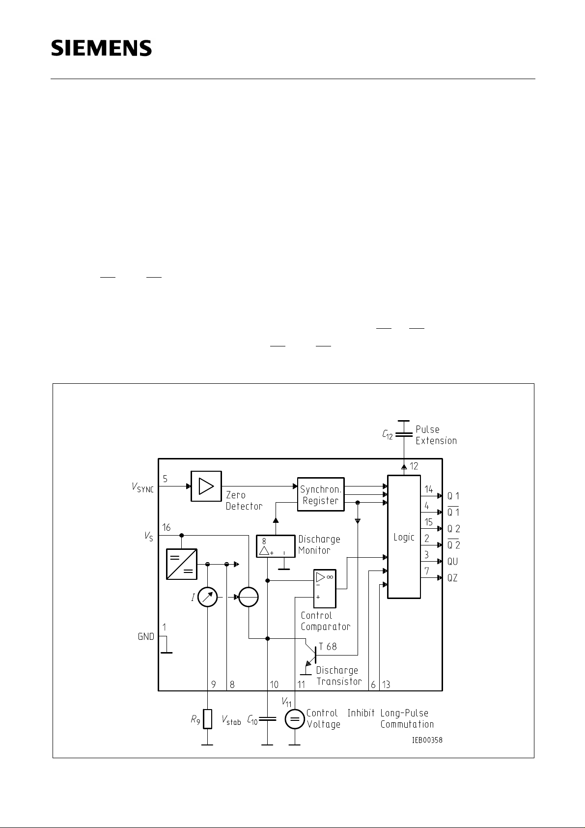
Functional Description
The synchronization signal is obtained via a high-ohmic resistance from the line voltage
(voltage V
synchronization register.
This synchronization register controls a ramp generator, the capacitor C
by a constant current (determined by R
11 (triggering angle ϕ), a signal is processed to the logic. Dependent on the magnitude of the
V
control voltage V
For every half wave, a positive pulse of approx. 30
Q 2. The pulse duration can be prolonged up to 180˚ via a capacitor C
to ground, pulses with a duration between
Outputs and supply the inverse signals of Q 1 and Q 2.
A signal of
A signal whichcorresponds to theNOR linkof Q 1 and Q 2 is available at output Q Z(pin 7).
The inhibit input can be used to disable outputs Q1, Q2 and , .
Pin 13 can be used to extend the outputs and to full pulse length (180˚ –
5). A zero voltage detector evaluates the zero passages and transfers them to the
10 of which is charged
9). If the ramp voltage V10 exceeds the control voltage
11, the triggering angle ϕ can be shifted within a phase angle of 0˚ to 180˚.
µs duration appears at the outputs Q 1 and
12. If pin 12 is connected
ϕ and 180˚ will result.
Q 1 Q 2
ϕ +180˚ which can be used for controlling an external logic,is available at pin 3.
Q 1 Q 2
Q 1 Q 2
ϕ).
Block Diagram
Semiconductor Group 2
TCA 785
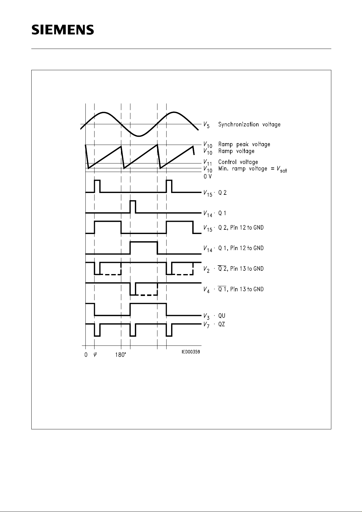
Pulse Diagram
Semiconductor Group 3
Absolute Maximum Ratings
TCA 785
Inhibit voltage
Control voltage
Voltage short-pulse circuit
Junction temperature
Storage temperature
Thermal resistance
system - air R
Operating Range
Limit Values
min. max.
S – 0.5 18
Q – 10 400
6
V
V11
V13
Q VS
Q VS
Tj
Tstg – 55
th SA 80
– 0.5
– 0.5
– 0.5
V
VS
VS
150
125
UnitParameter Symbol
VSupply voltage V
mAOutput current at pin 14, 15 I
S
V
V
V
µASynchronization input current V5 – 200 ± 200
VOutput voltage at pin 14, 15 V
mAOutput current at pin 2, 3, 4, 7 IQ 10
VOutput voltage at pin 2, 3, 4, 7 V
˚C
˚C
K/W
Characteristics
≤ VS ≤ 18 V; – 25 ˚C ≤ TA ≤ 85 ˚C; f = 50 Hz
8
IS 4.5 16.5 10
S1 … S6 open
11 = 0 V
V
10 = 47 nF; R 9 = 100 kΩ
C
Synchronization pin 5
Input current
2 varied
R
Offset voltage
5 rms
I
∆V5
A – 25 85
Limit Values Test
min. max.
typ.
UnitParameter Symbol
mASupply current consumption
30 1
200
75
µA
mV
VSupply voltage VS 818
HzOperating frequency f 10 500
˚CAmbient temperature T
Circuit
430
Control input pin 11
Control voltage range
Input resistance
V
R11
11
0.2 1
Semiconductor Group 4
V10 peak
V
k
Ω
515

Characteristics (cont’d)
≤ VS ≤ 18 V; – 25 ˚C ≤ TA ≤ 85 ˚C; f = 50 Hz
8
TCA 785
Ramp generator
Charge current
Max. ramp voltage
Saturation voltage at capacitor
Ramp resistance
Sawtooth return time
Inhibit pin 6
switch-over of pin 7
Outputs disabled
Outputs enabled
Signal transition time
Input current
6 = 8 V
V
Input current
6 = 1.7 V
V
Deviation of I10
R 9 = const.
S = 12 V; C10 = 47 nF
V
Deviation of I
10
R 9 = const.
S = 8 V to 18 V
V
Deviation of the ramp voltage
between 2 following
half-waves, V
S = const.
10
I
V10
V10
R9
tf
V6 L
V6 H
tr
I6 H
– I6L
10
I
I10
∆V10 max
Limit Values Test
min. max.
10
100
3
typ.
225
1000
2 – 2
V
350
300
80
4
1
80
– 5
– 20
3.3
3.3
500
150
± 1
2.5
5
800
200
5
20
UnitParameter Symbol
µA
V
mV
Ω
k
µs
V
V
µs
µA
µA
%
%
%
Circuit
1
1.6
1
1
1
1
1
1
1
1
1
Long pulse switch-over
pin 13
switch-over of S8
Short pulse at output
Long pulse at output
Input current
13 = 8 V
V
Input current
13 = 1.7 V
V
13 H
V
V13 L
I13 H
– I13 L
3.5
45
Outputs pin 2, 3, 4, 7
Reverse current
Q = VS
V
Saturation voltage
Q = 2 mA
I
ICEO
Vsat 0.1
Semiconductor Group 5
2.5
2.5
65
2
10
100
10
2
V
V
µA
µA
µA
V
1
1
1
1
2.6
2.60.4
 Loading...