

Siemens PSB2121-P, PSB2121-T Datasheet
General-Purpose Power Controller
(GPPC)
Features
● Switched mode DC/DC-converter
● CCITT ISDN compatible
● Low power dissipation
● Supply voltage range 8 to 70 V
● Programmable input undervoltage protection
● Programmable overcurrent protection
● Soft start
● Power housekeeping input
● Oscillator synchronization input/output
● High voltage CMOS-technology 70 V
PSB 2121
CMOS IC
P-DSO-20-1
P-DIP-16
Type Version Ordering Code Package
PSB 2121-P V A4/A5 Q67100-H8646 P-DIP-16
PSB 2121-T V A4/A5 Q67100-H6032 P-DSO-20-1 (SMD)
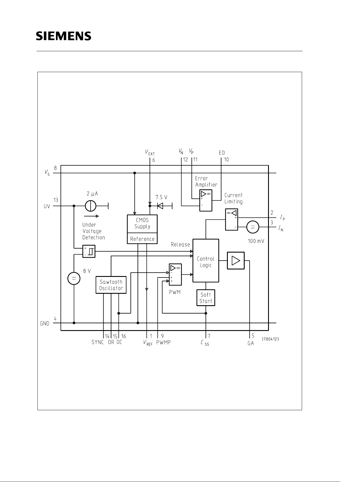
The PSB 2121 is a pulse width modulator circuit designed for fixed-frequency switching regulators
with very low power consumption.
In telephony and ISDN systems a high conversion yield is crucial to maintain functionality in all
supply conditions via “S” or “U” interfaces. The PSB 2121 design and technology realize high
conversion efficiency and low power dissipation.
It should be recognized that the PSB 2121 can also be used in numerous DC/DC-conversion
systems other than ISDN-power supplies.
Semiconductor Group 1 12.92
PSB 2121
The PSB 2121 Contains the Following Functional Blocks
● Undervoltage lockout
● Temperature compensated voltage reference
● Sawtooth oscillator
● Error amplifier
● Pulse width modulator
● Digital current limiting
● Soft start
● Double pulse inhibit
● Power driver
Together with few external components it provides a stable 5 V DC-supply for subscriber terminals
(TEs) or network terminations (NTs). It can also be programmed for higher output voltages, e.g. to
supply S-lines with 40 V.
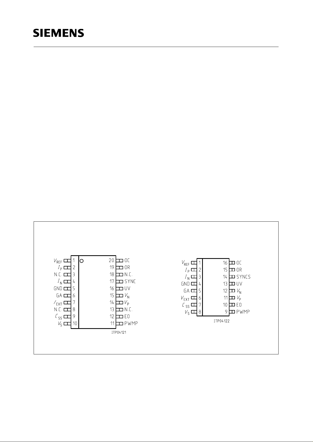
Pin Configurations
(top view)
P-DIP-16P-DSO-20
Semiconductor Group 2
Pin Definitions and Functions
PSB 2121
Pin No.
P-DSO
11
22
43
Pin No.
P-DIP
Symbol Input (I)
Output (O)
V
REF
I
P
I
N
O Reference
I Positive current
I Negative
Definition Function
Output of the 4.0 V reference
voltage
voltage.
When the voltage difference
sense
between these two pins exceeds
100 mV, the digital current limiting
current sense
becomes active.
5 4 GND I Ground All analog and digital signals are
referred to this pin.
6 5 GA O Gate Totem-pole output driver, has to be
connected with the gate of an
external power switch.
76
V
EXT
I/O External supply Output of the internal CMOS
supply. Via
V
the internal CMOS-
EXT
circuits can be supplied from an
external DC-supply in order to
reduce chip power dissipation.
97
C
SS
I Soft start
capacitor
The capacitor at this pin determines
the soft start characteristic.
10 8
11 9 PWMP I Pulse width
V
S
I Battery voltage VS is the positive input voltage.
Non-inverting input of the pulse
modulator
width modulator.
12 10 EO O Error amplifier output.
14 11
15 12
V
P
V
N
I Positive
voltage sense
I Negative
Non-inverting input of the error
amplifier.
Inverting input of the error amplifier.
voltage sense
16 13 UV I Undervoltage
detection
The undervoltage lockout can be
programmed via UV.
17 14 SYNC I/O Synchronization This pin can be used as an input for
synchronization of the oscillator to
an external frequency, or as an
output to synchronize multiple
devices.
19 15 OR I R-oscillator The external timing components of
20 16 OC I C-oscillator
the ramp generator are attached to
OR and OC.
Semiconductor Group 3
PSB 2121
Figure 1
GPPC Functional Diagram
Semiconductor Group 4
 Loading...