

Siemens ILQ3 Datasheet
FEATURES
• Current Transfer Ratio at IF=1.6 mA, 300% Min.
• High Collector-Emitter Voltage
•BV
CEO
=50 V
• Field-Effect Stable by TRansparent IOn Shield
(TRIOS)
• Double Molded Package Offer s Isolation Test Volta ge
5300 V AC
RMS
, 1 sec.
• Underwriters Lab File #E52744
• VDE 0884 Available with Option 1
V
DE
Maximum Ratings (Each Channel)
Emitter
Reverse Voltage............................................................. 6 V
Continuous Forward Current.....................................60 mA
Surge Current..............................................................2.5 A
Power Dissipation................................................... 100 mW
Derate Linearly from 25 °
C..................................1.3 mW/ ° C
Detector
Collector-Emitter Reverse Voltage................................ 50 V
Collector Current.......................................................50 mA
Collector Current (t<1 ms).......................................400 mA
Total Power Dissipation.......................................... 200 mW
Derate Linearly from 25 °
C..................................2.6 mW/ ° C
Package
Isolation Test Voltage (between emitter
and detector, refer to standard climate
23 °
C/50% RH, DIN50014)..................V
=5300 VAC
IO
RMS
Creepage............................................................min. 7 mm
Clearance............................................................min. 7 mm
Isolation Resistance
V
=500 V, T
IO
V
=500 V, T
IO
=25 ° C ......................................R
A
=100 ° C ....................................R
A
IO
IO
=10
=10
12
11
Ω
Ω
Power Dissipation................................................... 250 mW
Derate Linearly from 25 °
C..................................3.3 mW/ ° C
Storage Temperature Range........................ –40 to +150 °
Operating Temperature Range.....................–40 to +100 °
Junction Temperature................................................ 100 °
Soldering Temperature,
2 mm from case bottom........................................ 260 °
QUAD CHANNEL
ILQ3
PHOTOTRANSISTOR
OPTOCOUPLER
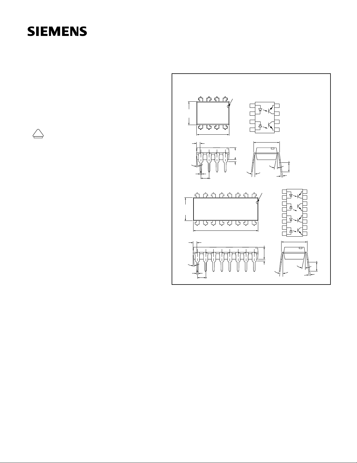
Package Dimensions in Inches (mm)
ILD3—Dual Channel
Pin One I.D.
12
34
Anode
.268 (6.81)
.255 (6.48)
4° Typ.
.022 (.56)
.018 (.46)
65
.390 (9.91)
.379 (9.63)
.045 (1.14)
.030 (.76)
.100 (2.54) Typ.
87
.150 (3.81)
.130 (3.30)
.040 (1.02)
.030 (.76 )
Cathode
Cathode
Anode
1
2
3
4
3°–9°
.305 Typ.
(7.75) Typ.
10° Typ.
.012 (.30)
.008 (.20)
ILQ3—Quad Channel
Pin One I.D.
.268 (6.81)
.255 (6.48)
.790 (20.07)
.779 (19.77 )
.150 (3.81)
.130 (3.30)
.040 (1.02)
.030 (.76 )
4° Typ.
.022 (.56)
.018 (.46)
.045 (1.14)
.030 (.76)
.100 (2.54) Typ.
DESCRIPTION
C
The ILD/Q3 are optically coupled isolated pairs employing GaAs
C
infrared LEDs and silicon NPN phototransistor. Signal information,
C
including a DC level, can be transmitted by the drive while maintaining a high degree of electrical isolation between input and output.
C
The ILD/Q3 are especially designed for driving medium-speed logic
and can be used to eliminate troublesome ground loop and noise
problems. Also these couplers can be used
transformers in many digital interface applications such as CRT
modulation. The ILD3 has two isolated channels in a single DIP
package and the ILQ3 has four isolated channels per package.
See Appnote 45, “How to Use Optocoupler Normalized Curves.”
Emitter
8
Collector
7
Collector
6
Emitter
5
.135 (3.43)
.115 (2.92)
1
Anode
2
Cathode
3
Cathode
4
Anode
5
Anode
6
Cathode
7
Cathode
8
Anode
.305 Typ.
(7.75) Typ.
10° Typ.
3°–9°
.012 (.30)
.008 (.20)
to replace relays and
16
15
14
13
12
11
10
9
Emitter
Collector
Collector
Emitter
Emitter
Collector
Collector
Emitter
.135 (3.43)
.115 (2.92)
5–158
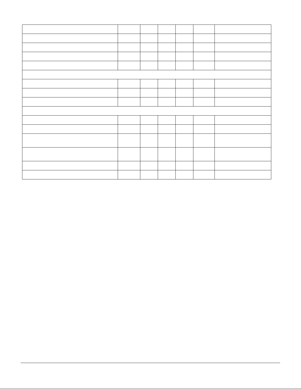
Characteristics
Emitter (IR GaAs) Symbol Min. Typ. Max. Unit Test Condition
Forward Voltage V
Reverse Current I
Capacitance C
Thermal Resistance, Junction to Lead R
F
R
0
THJL
1.25 1.65 V I
0.01 10
25 pF V
750
Detector
Collector-Emitter Leakage Current I
Capacitance C
Thermal Resistance, Junction to Lead R
CEO
CE
THJL
570nAV
6.8 pF V
500
Package Transfer Characteristics (Each Channel)
Saturated Current Transfer Ratio, ILD/Q3-1 CTR
Saturated Current Transfer Ratio, ILD/Q3-2 CTR
300 % I
SAT
100 % I
SAT
Common Mode Rejection Output High CMH 5000 V/
Common Mode Rejection Output Low CML 5000 V/
Common Mode Coupling Capacitance C
Package Capacitance C
CM
IO
0.01 pF
0.8 pF V
=60 mA
F
µ
AV
=6 V
R
=0 V, f=1 MHz
R
° C/W
=15 V
CE
=5 V, f=1 MHz
CE
° C/W
=1.6 mA, V
F
=1.0 mA, V
F
µ sV
µ sV
=50 V
CM
I
=0 mA
F
=50 V
CM
I
=0 mA
F
=0 V, f=1 MHz
IO
P-P
P-P
CE
CE
, R
, R
=0.4 V
=0.4 V
L
L
=10 k Ω ,
=10 k Ω ,
5–159
ILD/Q3
 Loading...